WO2021187063A1 - 電気装置 - Google Patents
電気装置 Download PDFInfo
- Publication number
- WO2021187063A1 WO2021187063A1 PCT/JP2021/007597 JP2021007597W WO2021187063A1 WO 2021187063 A1 WO2021187063 A1 WO 2021187063A1 JP 2021007597 W JP2021007597 W JP 2021007597W WO 2021187063 A1 WO2021187063 A1 WO 2021187063A1
- Authority
- WO
- WIPO (PCT)
- Prior art keywords
- support
- component
- substrate
- metal
- metal terminal
- Prior art date
- Legal status (The legal status is an assumption and is not a legal conclusion. Google has not performed a legal analysis and makes no representation as to the accuracy of the status listed.)
- Ceased
Links
Images



Classifications
-
- H—ELECTRICITY
- H05—ELECTRIC TECHNIQUES NOT OTHERWISE PROVIDED FOR
- H05K—PRINTED CIRCUITS; CASINGS OR CONSTRUCTIONAL DETAILS OF ELECTRIC APPARATUS; MANUFACTURE OF ASSEMBLAGES OF ELECTRICAL COMPONENTS
- H05K1/00—Printed circuits
- H05K1/18—Printed circuits structurally associated with non-printed electric components
-
- H—ELECTRICITY
- H05—ELECTRIC TECHNIQUES NOT OTHERWISE PROVIDED FOR
- H05K—PRINTED CIRCUITS; CASINGS OR CONSTRUCTIONAL DETAILS OF ELECTRIC APPARATUS; MANUFACTURE OF ASSEMBLAGES OF ELECTRICAL COMPONENTS
- H05K3/00—Apparatus or processes for manufacturing printed circuits
- H05K3/30—Assembling printed circuits with electric components, e.g. with resistors
- H05K3/32—Assembling printed circuits with electric components, e.g. with resistors electrically connecting electric components or wires to printed circuits
- H05K3/34—Assembling printed circuits with electric components, e.g. with resistors electrically connecting electric components or wires to printed circuits by soldering
Definitions
- the present invention relates to an electrical device.
- This application claims priority based on Japanese Application No. 2020-045530 filed on March 16, 2020, and incorporates all the contents described in the Japanese application.
- reflow soldering may be performed.
- a paste-like solder is applied to a substrate so as to cover a through hole provided in the substrate.
- the lead terminal of the electronic component metal terminal of the electrical component
- the substrate is sent to the reflow oven to heat the solder.
- the solder melted by heating flows into the through holes. After that, the solder solidifies between the metal film and the lead terminal, so that the electric component is mounted on the substrate.
- the electric device includes a substrate having a connection hole having a metal film on the inner peripheral surface and a conductive pattern electrically connected to the metal film, a component body, and the component.
- An electric component having a metal terminal that protrudes from the main body and is inserted into the connection hole and soldered to the metal film is provided, and a support hole is provided at a position different from the connection hole on the substrate.
- the electrical component further has support legs that project from the component body and are inserted into the support holes to support the component body.
- FIG. 1 is a cross-sectional view of an electric device according to an embodiment.
- FIG. 2 is a cross-sectional view taken along the line II-II in FIG.
- FIG. 3 is a perspective view of an electrical component.
- FIG. 4 is an explanatory diagram of a manufacturing procedure of an electric device.
- FIG. 5 is an explanatory diagram of a manufacturing procedure of an electric device.
- the electric device includes a substrate provided with a connection hole having a metal film on the inner peripheral surface, a conductive pattern electrically connected to the metal film, and a component body. And an electrical component having a metal terminal that protrudes from the component body and is inserted into the connection hole and soldered to the metal film, and a support hole is provided at a position different from the connection hole on the substrate.
- the electrical component further has support legs that project from the component body and are inserted into the support holes to support the component body.
- the substrate is provided with a support hole.
- the electrical component has a component body, metal terminals, and support legs. Since the support legs are inserted into the support holes of the substrate to support the component body, the posture of the electrical component can be stabilized. That is, the inclination of the electrical component can be suppressed. Since the electric component does not tilt significantly, the electric component can be mounted on the substrate satisfactorily.
- the support leg is made of metal and branches from the middle of the protruding direction of the metal terminal, and a portion on the tip side of the branch portion of the metal terminal is inserted into the connection hole. ..
- the metal support legs are branched from the middle of the metal terminals, the number of parts can be reduced.
- the electrical component has two metal terminals and two support legs.
- Each metal terminal is bifurcated.
- the portion on the tip side of each of the two metal terminals and the two support legs are arranged in one direction so that the two tip side portions are located on the outside and the two support legs are located on the inside. I'm out.
- connection hole of the board corresponds to the part on the tip side of the branch part of the metal terminal, and the support hole of the board corresponds to the support leg. Therefore, in the substrate, the two connection holes and the two support holes are arranged in a row so that the connection holes are located on the outside and the support holes are located on the inside. Therefore, it is easier to provide a spatial margin in the peripheral edge of the opening of the connection hole than in the peripheral edge of the opening of the support hole. As a result, the degree of freedom in arranging the conductive pattern is high.
- the area of the cross section of the tip side portion orthogonal to the protruding direction is larger than the area of the cross section of the support leg orthogonal to the protruding direction.
- the cross-sectional area of the tip side portion is larger than that of the branch portion of the metal terminal, the electrical resistance of the portion inserted into the connection hole of the metal terminal at the time of conduction can be reduced.
- the support legs are electrically open.
- the support legs are electrically open, it is not necessary to reduce the electrical resistance of the support legs at the time of conduction. Therefore, since the cross-sectional area of the support legs can be reduced, the amount of metal material for providing the support legs can be reduced.
- the electric component is a fuse.
- the electric component which is a fuse can be mounted on the substrate well, the electric device can be protected from the overcurrent.
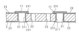
- FIG. 1 is a cross-sectional view of an electric device according to an embodiment.
- 1 is an electric device, and the electric device 1 includes a substrate 2 and an electric component 3.
- FIG. 2 is a cross-sectional view taken along the line II-II in FIG.
- the substrate 2 is made of a synthetic resin having electrical insulation.
- the substrate 2 is provided with two connection holes 21 and two support holes 22.
- the two connection holes 21 and the two support holes 22 are arranged in one direction with appropriate lengths separated from each other.
- Two support holes 22 are arranged between the two connection holes 21.
- connection hole 21 penetrates the substrate 2 in the thickness direction.
- the connection hole 21 is circular in a plan view.
- the connection hole 21 has a metal film 211.
- the metal film 211 is provided on the inner peripheral surface of the connection hole 21.
- Such a connection hole 21 is a through hole.
- the support hole 22 penetrates the substrate 2 in the thickness direction.
- the support hole 22 is circular in a plan view.
- the inner diameter of the support hole 22 is smaller than the inner diameter of the connection hole 21. No metal film is provided on the inner peripheral surface of the support hole 22.
- a plurality of conductive patterns 23 are provided on both sides of the substrate 2.
- the conductive pattern 23 is a metal film.
- the conductive pattern 23 has a land 231.
- Lands 231 are provided on both sides of the substrate 2 at the peripheral edge of the opening of the connection hole 21 over the entire circumference.
- the land 231 is continuous with the metal film 211 of the connection hole 21.
- the thickness of each of the metal film 211 and the conductive pattern 23 is negligibly small compared to the thickness of the substrate 2. However, in the figure, the thickness of each of the metal film 211 and the conductive pattern 23 is exaggerated in order to make it easier to see.
- FIG. 3 is a perspective view of the electrical component 3.
- the electric component 3 includes a component body 4 and two metal terminals 5.
- the component body 4 includes an exterior 41 and a fuse element 42.
- the exterior 41 is made of an electrically insulating synthetic resin and has a rectangular plate shape that is long in one direction.
- the fuse element 42 is an elongated conducting wire and is sealed in the exterior 41.
- Each metal terminal 5 projects outward from one of the four end faces of the component body 4 extending in the longitudinal direction of the component body 4.
- the metal terminal 5 is made of metal and has a rectangular plate shape that is long in the protruding direction of the metal terminal 5.
- the thickness direction of the metal terminal 5 is along the thickness direction of the component body 4.
- the metal terminal 5 is bifurcated from the middle of the protruding direction.
- the branch portion 5a of the metal terminal 5 is separated from the exterior 41 by an appropriate length in the protruding direction of the metal terminal 5.
- an insertion portion 51 one is referred to as an insertion portion 51, and the other is referred to as a support leg 52. That is, the support leg 52 is made of metal and branches from the middle of the protruding direction of the metal terminal 5.
- the insertion portion 51 and the support legs 52 of the metal terminal 5 are adjacent to each other in the longitudinal direction of the component body 4. As shown in FIG. 2, the cross section of each of the insertion portion 51 and the support leg 52 orthogonal to the protruding direction of the metal terminal 5 has a rectangular shape. The cross-sectional area of the insertion portion 51 is larger than the cross-sectional area of the support leg 52.
- the two metal terminals 5 project from the same end face of the component body 4 in the same direction and are separated from each other in the longitudinal direction of the component body 4.
- the two insertion portions 51 and the two support legs 52 are arranged in the longitudinal direction of the component body 4, and the two support legs 52 are arranged between the two insertion portions 51. There is.
- the extending portion 53 extends from the base end of the metal terminal 5 in the direction opposite to the protruding direction of the metal terminal 5.
- the extending portion 53 is sealed in the exterior 41 of the component main body 4.
- the fuse element 42 of the component body 4 is electrically connected to the two metal terminals 5.
- the electrical component 3 as described above is a fuse.
- the distance between the connecting holes 21 and the support holes 22 adjacent to each other and the distance between the insertion portions 51 and the support legs 52 adjacent to each other are the same. Further, the distance between the two support holes 22 and the distance between the two support legs 52 are the same as each other.
- the insertion portion 51 can be inserted into the connection hole 21 and cannot be inserted into the support hole 22.
- the support legs 52 can be inserted into the support holes 22.
- the insertion portion 51 is inserted into the connection hole 21 from one surface (hereinafter referred to as an upper surface) side of the substrate 2.
- the solder 11 is interposed between the metal terminal 5, the metal film 211, and the land 231. However, the illustration of the solder 11 in FIG. 2 is omitted.
- the support legs 52 are inserted into the support holes 22 from the upper surface side of the substrate 2.
- the exterior 41 and the metal terminal 5 of the component body 4 are arranged in a direction orthogonal to the substrate 2.
- the end surface (hereinafter referred to as the lower end surface) on which the metal terminal 5 of the exterior 41 protrudes faces the upper surface of the substrate 2. Since the branch portion 5a of the metal terminal 5 is separated downward from the lower end surface of the exterior 41 by an appropriate length, there is no possibility that the lower end surface of the exterior 41 will come into contact with the upper surface of the substrate 2.
- connection hole 21 is sufficiently larger than the diagonal length of the cross section of the insertion portion 51.
- the inner diameter of the support hole 22 is about the same as the diagonal length of the cross section of the support leg 52.
- FIGS. 4 and 5 are explanatory views of a manufacturing procedure of the electric device 1.
- the electric component 3 is mounted on the substrate 2, as shown in FIG. 4, first, the upper surface of the substrate 2 is turned upward, and the paste-like solder 11 covers the connection hole 21 from the upper side. It is applied to the peripheral edge of the opening of 21.
- the two metal terminals 5 of the electric component 3 are directed downward.
- the two insertion portions 51 are inserted into the two connection holes 21 downward from the upper side of the substrate 2, and the two support legs 52 are inserted into the two support holes 22 downward from the upper side of the substrate 2.
- the exterior 41 of the component body 4 of the electrical component 3 is arranged in a direction orthogonal to the substrate 2. Further, the lower end surface of the exterior 41 is separated from the upper surface of the substrate 2 upward.
- connection hole 21 Since the inner diameter of the connection hole 21 is sufficiently larger than the diagonal length of the cross section of the insertion portion 51, there is a sufficient gap between the inner peripheral surface of the connection hole 21 and the insertion portion 51. Since the inner diameter of the support hole 22 is about the same as the diagonal length of the cross section of the support leg 52, there is almost no gap between the inner peripheral surface of the support hole 22 and the support leg 52.
- the substrate 2 After inserting the metal terminal 5, the substrate 2 is sent to a reflow furnace (not shown) to heat the solder 11.
- the solder 11 melted by heating becomes familiar with the land 231 and flows into the connection hole 21 through the metal film 211 continuous with the land 231. Since there is a sufficient gap between the inner peripheral surface of the connection hole 21 and the insertion portion 51, the solder 11 is formed between the inner peripheral surface of the connection hole 21 and the insertion portion 51 of the metal terminal 5 during the soldering process. Easy to flow in.
- the solder 11 that has flowed into the connection hole 21 is interposed between the metal film 211 and the insertion portion 51 of the metal terminal 5. After that, as the solder 11 solidifies, the insertion portion 51 of the metal terminal 5 is electrically connected to the metal film 211 (and thus the conductive pattern 23) via the solder 11 and fixed to the substrate 2. That is, the electric component 3 is mounted on the substrate 2. Since the cross-sectional area of the insertion portion 51 of the metal terminal 5 is large, the electrical resistance of the insertion portion 51 at the time of conduction can be reduced.
- the support legs 52 of the metal terminal 5 are not electrically connected to the conductive pattern 23 via the solder 11. That is, the support legs 52 are electrically open. Since the support legs 52 are electrically open, it is not necessary to reduce the electrical resistance of the support legs 52 during conduction. Therefore, since the cross-sectional area of the support legs 52 can be reduced, the metal material for providing the support legs 52 can be reduced. Since the support legs 52 are branched from the middle of the metal terminal 5, the number of parts can be reduced.
- the component main body 4 is separated from the substrate 2, it is unlikely that a defect of the solder 11 will occur during soldering. If the component body 4 is in contact with the substrate 2 and the component body 4 is in contact with the paste-like solder 11 applied to the substrate 2 at the time of soldering, there is a problem that solder balls are likely to be generated. There is. Further, since the component main body 4 is separated from the substrate 2, an appropriate solder fillet is easily formed at the time of soldering. This contributes to good mounting of the electrical component 3 on the substrate 2. As a result, the long-term reliability of the substrate 2 on which the electric component 3 is mounted can be improved.
- One metal terminal 5 of the electric component 3 is electrically connected to an in-vehicle power supply (not shown) via one conductive pattern 23.
- the other metal terminal 5 of the electrical component 3 is electrically connected to an in-vehicle load (not shown) via another conductive pattern 23.
- the electric component 3 is electrically interposed between the vehicle-mounted power supply and the vehicle-mounted load. The current flowing between the vehicle-mounted power supply and the vehicle-mounted load passes through the two metal terminals 5 and the fuse element 42 of the electric component 3.
- a plurality of electric components 3 are mounted on the board 2. Since the component body 4 has a plate shape, the plurality of electric components 3 can be closely arranged in the thickness direction of the component body 4. As a result, it is possible to obtain an electric device 1 that is compact in the thickness direction of the component body 4. Since the internal space of the vehicle is limited, the compact electric device 1 is useful.
- connection holes 21 and the two support holes 22 are arranged in a row so that the connection holes 21 are located on the outside and the support holes 22 are located on the inside. Therefore, it is easier to provide a spatial margin in the peripheral edge of the opening of the connection hole 21 than in the peripheral edge of the opening of the support hole 22. Therefore, the degree of freedom in arranging the conductive pattern 23 is high. Further, the plurality of electric components 3 can be closely arranged in the thickness direction of the component body 4 without interfering with the conductive pattern 23.
- the electric component 3 is not limited to the configuration in which the component body 4 includes the fuse element 42.
- the electric component 3 may have a configuration in which the component body 4 includes a switching element.
- the number of metal terminals 5 included in the electric component 3 is not limited to two.
- the metal terminal 5 is not limited to a plate shape, and may be, for example, a rod shape.
- the solder may be heated by using something other than hot air (for example, infrared rays). Further, the soldering of the metal terminal 5 is not limited to the soldering by reflow. In any case, when the component body 4 tries to incline by receiving an external force in the soldering process, the support legs 52 abut on the inner peripheral surface of the support hole 22 to support the component body 4, so that the electrical component 3 is supported. The inclination of the soldering can be suppressed.
- the number of support legs 52 is not limited to two, and may be one. However, if there are a plurality of support legs 52, the posture of the electric component 3 can be further stabilized.
- connection hole 21 or the support hole 22 of the substrate 2 does not have to penetrate the substrate 2.
- the shape of the connection hole 21 or the support hole 22 is not limited to a circular shape, and may be, for example, an elliptical shape.
- the support legs 52 may have a tapered shape in order to further facilitate the insertion of the support legs 52 of the metal terminals 5 into the support holes 22 of the substrate 2.
- the support legs 52 may be press-fitted into the support holes 22.
- the support legs 52 may project directly from the component body 4.
Landscapes
- Engineering & Computer Science (AREA)
- Microelectronics & Electronic Packaging (AREA)
- Manufacturing & Machinery (AREA)
- Structures For Mounting Electric Components On Printed Circuit Boards (AREA)
- Electric Connection Of Electric Components To Printed Circuits (AREA)
Abstract
本開示の一態様に係る電気装置は、内周面に金属膜を有する接続穴、及び前記金属膜に電気的に接続されている導電パターンが設けられている基板と、部品本体、及び該部品本体から突出し、前記接続穴に挿入されて前記金属膜に半田付けされている金属端子を有する電気部品とを備え、前記基板における前記接続穴とは異なる位置に支持穴が設けられており、前記電気部品は、前記部品本体から突出し、前記支持穴に挿入されて前記部品本体を支持する支持脚を更に有する。
Description
本発明は、電気装置に関する。
本出願は、2020年3月16日出願の日本出願第2020-045530号に基づく優先権を主張し、前記日本出願に記載された全ての記載内容を援用するものである。
本出願は、2020年3月16日出願の日本出願第2020-045530号に基づく優先権を主張し、前記日本出願に記載された全ての記載内容を援用するものである。
電気部品が基板に実装される場合、リフローによる半田付けが行なわれることがある。
特許文献1に記載されている電子部品の実装方法においては、まず、基板に設けられているスルーホール(Plated Through Hole )を覆うようにして、ペースト状の半田が基板に塗布される。次に、電子部品のリード端子(電気部品の金属端子)がスルーホールに挿入される。スルーホールの内周面と電子部品のリード端子との間には十分な隙間がある。更に、基板がリフロー炉に送られ、半田が加熱される。加熱によって熔融した半田は、スルーホールに流入する。その後、金属膜とリード端子との間で半田が固化することによって、電気部品が基板に実装される。
特許文献1に記載されている電子部品の実装方法においては、まず、基板に設けられているスルーホール(Plated Through Hole )を覆うようにして、ペースト状の半田が基板に塗布される。次に、電子部品のリード端子(電気部品の金属端子)がスルーホールに挿入される。スルーホールの内周面と電子部品のリード端子との間には十分な隙間がある。更に、基板がリフロー炉に送られ、半田が加熱される。加熱によって熔融した半田は、スルーホールに流入する。その後、金属膜とリード端子との間で半田が固化することによって、電気部品が基板に実装される。
本開示の一態様に係る電気装置は、内周面に金属膜を有する接続穴、及び前記金属膜に電気的に接続されている導電パターンが設けられている基板と、部品本体、及び該部品本体から突出し、前記接続穴に挿入されて前記金属膜に半田付けされている金属端子を有する電気部品とを備え、前記基板における前記接続穴とは異なる位置に支持穴が設けられており、前記電気部品は、前記部品本体から突出し、前記支持穴に挿入されて前記部品本体を支持する支持脚を更に有する。
[本開示が解決しようとする課題]
スルーホールの内周面と電子部品のリード端子との間に十分な隙間があるので、半田が固化する前は、電気部品の姿勢が不安定である。故に、半田付けの過程で、外力を受けた電気部品が大きく傾斜するおそれがある。電気部品が大きく傾斜した状態では、電気部品を基板に良好に実装することができない。
スルーホールの内周面と電子部品のリード端子との間に十分な隙間があるので、半田が固化する前は、電気部品の姿勢が不安定である。故に、半田付けの過程で、外力を受けた電気部品が大きく傾斜するおそれがある。電気部品が大きく傾斜した状態では、電気部品を基板に良好に実装することができない。
そこで、電気部品を基板に良好に実装することができる電気装置を提供することを目的とする。
[本開示の効果]
本開示によれば、電気部品を基板に良好に実装することができる電気装置を提供することが可能となる。
本開示によれば、電気部品を基板に良好に実装することができる電気装置を提供することが可能となる。
[本開示の実施態様の説明]
最初に本開示の実施態様を列記して説明する。また、以下に記載する実施形態の少なくとも一部を任意に組み合わせてもよい。
最初に本開示の実施態様を列記して説明する。また、以下に記載する実施形態の少なくとも一部を任意に組み合わせてもよい。
(1)本開示の一態様に係る電気装置は、内周面に金属膜を有する接続穴、及び前記金属膜に電気的に接続されている導電パターンが設けられている基板と、部品本体、及び該部品本体から突出し、前記接続穴に挿入されて前記金属膜に半田付けされている金属端子を有する電気部品とを備え、前記基板における前記接続穴とは異なる位置に支持穴が設けられており、前記電気部品は、前記部品本体から突出し、前記支持穴に挿入されて前記部品本体を支持する支持脚を更に有する。
本態様にあっては、基板に支持穴が設けられている。
電気部品は部品本体、金属端子、及び支持脚を有する。支持脚が基板の支持穴に挿入されて部品本体を支持するので、電気部品の姿勢を安定させることができる。即ち、電気部品の傾斜を抑制することができる。電気部品が大きく傾斜することがないので、電気部品を基板に良好に実装することができる。
電気部品は部品本体、金属端子、及び支持脚を有する。支持脚が基板の支持穴に挿入されて部品本体を支持するので、電気部品の姿勢を安定させることができる。即ち、電気部品の傾斜を抑制することができる。電気部品が大きく傾斜することがないので、電気部品を基板に良好に実装することができる。
(2)前記支持脚は金属製であり、前記金属端子の突出方向の中途から分岐しており、前記金属端子の分岐部よりも先端側の部分が前記接続穴に挿入されている構成が好ましい。
本態様にあっては、金属製の支持脚が金属端子の中途から分岐しているので、部品点数を削減することができる。
(3)前記金属端子は複数あり、前記支持脚は各金属端子に設けられている構成が好ましい。
本態様にあっては、支持脚が複数あるので、電気部品の姿勢を更に安定させることができる。
(4)前記金属端子は2つあり、前記支持脚は各金属端子に1つあり、2つの前記先端側の部分と2つの前記支持脚とが一方向に並んでおり、2つの前記先端側の部分の間に2つの前記支持脚が配されている構成が好ましい。
本態様にあっては、電気部品が2つの金属端子及び2つの支持脚を有する。
各金属端子は二股である。2つの金属端子それぞれの分岐部よりも先端側の部分及び2つの支持脚は、2つの先端側の部分が外側に位置し、2つの支持脚が内側に位置するようにして、一方向に並んでいる。
各金属端子は二股である。2つの金属端子それぞれの分岐部よりも先端側の部分及び2つの支持脚は、2つの先端側の部分が外側に位置し、2つの支持脚が内側に位置するようにして、一方向に並んでいる。
基板の接続穴は、金属端子の分岐部よりも先端側の部分に対応し、基板の支持穴は、支持脚に対応する。故に、基板においては、2つの接続穴及び2つの支持穴が、接続穴が外側に位置し、支持穴が内側に位置するようにして、一列に並んでいる。従って、接続穴の開口の周縁部の方が、支持穴の開口の周縁部よりも、空間的な余裕を設けやすい。この結果、導電パターンの配置の自由度が高い。
(5)前記先端側の部分の前記突出方向に直交する断面の面積は、前記支持脚の前記突出方向に直交する断面の面積よりも大きい構成が好ましい。
本態様にあっては、金属端子の分岐部よりも先端側の部分の断面積が大きいので、導通時における金属端子の接続穴に挿入されている部分の電気抵抗を小さくすることができる。
(6)前記支持脚は電気的に開放されている構成が好ましい。
本態様にあっては、支持脚が電気的に開放されているので、導通時における支持脚の電気抵抗を小さくする必要はない。故に、支持脚の断面積を小さくすることができるので、支持脚を設けるための金属材料を削減することができる。
(7)前記電気部品はヒューズである構成が好ましい。
本態様にあっては、ヒューズである電気部品を基板に良好に実装することができるので、電気機器を過電流から保護することができる。
[本開示の実施形態の詳細]
本開示の実施形態に係る電気装置の具体例を、以下に図面を参照しつつ説明する。なお、本開示はこれらの例示に限定されるものではなく、請求の範囲によって示され、請求の範囲と均等の意味および範囲内でのすべての変更が含まれることが意図される。
本開示の実施形態に係る電気装置の具体例を、以下に図面を参照しつつ説明する。なお、本開示はこれらの例示に限定されるものではなく、請求の範囲によって示され、請求の範囲と均等の意味および範囲内でのすべての変更が含まれることが意図される。
図1は、実施形態に係る電気装置の断面図である。
図中1は電気装置であり、電気装置1は基板2及び電気部品3を備える。
図中1は電気装置であり、電気装置1は基板2及び電気部品3を備える。
1.基板2の構成
図2は、図1におけるII-II線による断面図である。
基板2は電気絶縁性を有する合成樹脂製である。
図1及び図2に示すように、基板2には2つの接続穴21及び2つの支持穴22が設けられている。2つの接続穴21及び2つの支持穴22は、互いに適長離隔して、一方向に並んでいる。2つの接続穴21の間に2つの支持穴22が配されている。
図2は、図1におけるII-II線による断面図である。
基板2は電気絶縁性を有する合成樹脂製である。
図1及び図2に示すように、基板2には2つの接続穴21及び2つの支持穴22が設けられている。2つの接続穴21及び2つの支持穴22は、互いに適長離隔して、一方向に並んでいる。2つの接続穴21の間に2つの支持穴22が配されている。
接続穴21は基板2を厚さ方向に貫通している。接続穴21は平面視で円形である。接続穴21は金属膜211を有する。金属膜211は接続穴21の内周面に設けられている。このような接続穴21はスルーホールである。
支持穴22は基板2を厚さ方向に貫通している。支持穴22は平面視で円形である。支持穴22の内径は接続穴21の内径よりも小さい。支持穴22の内周面には金属膜が設けられていない。
支持穴22は基板2を厚さ方向に貫通している。支持穴22は平面視で円形である。支持穴22の内径は接続穴21の内径よりも小さい。支持穴22の内周面には金属膜が設けられていない。
基板2の両面それぞれには、複数の導電パターン23が設けられている。導電パターン23は金属膜である。
導電パターン23はランド231を有する。基板2の両面それぞれにおいて、ランド231は、接続穴21の開口の周縁部に、全周にわたって設けられている。ランド231は接続穴21の金属膜211に連続している。
基板2の厚さに比べて、金属膜211及び導電パターン23それぞれの厚さは無視できるほど小さい。ただし、図においては、金属膜211及び導電パターン23それぞれを見易くするために、それぞれの厚さが誇張されている。
導電パターン23はランド231を有する。基板2の両面それぞれにおいて、ランド231は、接続穴21の開口の周縁部に、全周にわたって設けられている。ランド231は接続穴21の金属膜211に連続している。
基板2の厚さに比べて、金属膜211及び導電パターン23それぞれの厚さは無視できるほど小さい。ただし、図においては、金属膜211及び導電パターン23それぞれを見易くするために、それぞれの厚さが誇張されている。
2.電気部品3の構成
図3は、電気部品3の斜視図である。
図1及び図3に示すように、電気部品3は部品本体4及び2つの金属端子5を備える。
部品本体4は外装41及びヒューズエレメント42を備える。外装41は電気絶縁性を有する合成樹脂製であり、一方向に長い矩形の板状をなす。ヒューズエレメント42は細長い導線であり、外装41に封止されている。
図3は、電気部品3の斜視図である。
図1及び図3に示すように、電気部品3は部品本体4及び2つの金属端子5を備える。
部品本体4は外装41及びヒューズエレメント42を備える。外装41は電気絶縁性を有する合成樹脂製であり、一方向に長い矩形の板状をなす。ヒューズエレメント42は細長い導線であり、外装41に封止されている。
各金属端子5は、部品本体4の4つの端面の内、部品本体4の長手方向に延びる一の端面から外向きに突出している。
金属端子5は金属製であり、金属端子5の突出方向に長い矩形の板状をなす。金属端子5の厚さ方向は部品本体4の厚さ方向に沿う。
金属端子5は金属製であり、金属端子5の突出方向に長い矩形の板状をなす。金属端子5の厚さ方向は部品本体4の厚さ方向に沿う。
金属端子5は、突出方向の中途から二股に分岐している。金属端子5の分岐部5aは、外装41から金属端子5の突出方向に適長離隔している。
以下では、金属端子5の分岐部5aから先端側の2つの部分の内、一方を挿入部51といい、他方を支持脚52という。即ち、支持脚52は金属製であり、金属端子5の突出方向の中途から分岐している。
以下では、金属端子5の分岐部5aから先端側の2つの部分の内、一方を挿入部51といい、他方を支持脚52という。即ち、支持脚52は金属製であり、金属端子5の突出方向の中途から分岐している。
金属端子5の挿入部51及び支持脚52は、互いに部品本体4の長手方向に隣り合っている。図2に示すように、挿入部51及び支持脚52それぞれの、金属端子5の突出方向に直交する断面は矩形状をなす。挿入部51の断面積は支持脚52の断面積よりも大きい。
図1及び図3に示すように、2つの金属端子5は、部品本体4の同一の端面から同じ向きに突出しており、部品本体4の長手方向に互いに離隔している。図1~図3に示すように、2つの挿入部51及び2つの支持脚52は部品本体4の長手方向に並んでおり、2つの挿入部51の間に2つの支持脚52が配されている。
図1及び図3に示すように、金属端子5の基端から、金属端子5の突出方向の逆向きに延出部53が延び出ている。延出部53は、部品本体4の外装41に封止されている。部品本体4のヒューズエレメント42は、2つの金属端子5に電気的に接続されている。
以上のような電気部品3はヒューズである。
以上のような電気部品3はヒューズである。
3.電気装置1の構成
図1及び図2に示すように、基板2の2つの接続穴21と、電気部品3の2つの挿入部51とが互いに対応している。同様に、2つの支持穴22と2つの支持脚52とが互いに対応している。
図1及び図2に示すように、基板2の2つの接続穴21と、電気部品3の2つの挿入部51とが互いに対応している。同様に、2つの支持穴22と2つの支持脚52とが互いに対応している。
具体的には、互いに隣り合う接続穴21及び支持穴22間の距離と、互いに隣り合う挿入部51及び支持脚52間の距離とが互いに同じである。また、2つの支持穴22間の距離と2つの支持脚52間の距離とが互いに同じである。挿入部51は接続穴21に挿入可能であり、支持穴22には挿入不可能である。支持脚52は支持穴22に挿入可能である。
挿入部51は基板2の一面(以下、上面という)側から接続穴21に挿入されている。金属端子5と金属膜211及びランド231との間に半田11が介在している。ただし、図2における半田11の図示は省略している。
支持脚52は基板2の上面側から支持穴22に挿入されている。
部品本体4の外装41及び金属端子5は、基板2に直交する向きに配されている。外装41の金属端子5が突出している端面(以下、下端面という)は、基板2の上面に対向している。金属端子5の分岐部5aは、外装41の下端面から下方に適長離隔しているので、外装41の下端面が基板2の上面に接触するおそれはない。
支持脚52は基板2の上面側から支持穴22に挿入されている。
部品本体4の外装41及び金属端子5は、基板2に直交する向きに配されている。外装41の金属端子5が突出している端面(以下、下端面という)は、基板2の上面に対向している。金属端子5の分岐部5aは、外装41の下端面から下方に適長離隔しているので、外装41の下端面が基板2の上面に接触するおそれはない。
接続穴21の内径は、挿入部51の断面の対角線の長さよりも十分に大きい。
支持穴22の内径は、支持脚52の断面の対角線の長さと同程度である。
支持穴22の内径は、支持脚52の断面の対角線の長さと同程度である。
4.電気部品3の基板2への実装
図4及び図5は、電気装置1の製造手順の説明図である。
電気部品3が基板2に実装される場合、図4に示すように、まず、基板2の上面が上に向けられ、ペースト状の半田11が、上側から接続穴21を覆うようにして接続穴21の開口の周縁部に塗布される。
図4及び図5は、電気装置1の製造手順の説明図である。
電気部品3が基板2に実装される場合、図4に示すように、まず、基板2の上面が上に向けられ、ペースト状の半田11が、上側から接続穴21を覆うようにして接続穴21の開口の周縁部に塗布される。
半田11の塗布後、図5に示すように、電気部品3の2つの金属端子5が下に向けられる。2つの挿入部51が2つの接続穴21に基板2の上側から下向きに挿入されると共に、2つの支持脚52が2つの支持穴22に基板2の上側から下向きに挿入される。この結果、電気部品3の部品本体4の外装41は、基板2に直交する向きに配される。また、外装41の下端面が基板2の上面から上側に離隔する。
接続穴21の内径は、挿入部51の断面の対角線の長さよりも十分に大きいので、接続穴21の内周面と挿入部51との間には十分な隙間がある。
支持穴22の内径は、支持脚52の断面の対角線の長さと同程度なので、支持穴22の内周面と支持脚52との間にはほとんど隙間がない。
支持穴22の内径は、支持脚52の断面の対角線の長さと同程度なので、支持穴22の内周面と支持脚52との間にはほとんど隙間がない。
金属端子5の挿入後、基板2が図示しないリフロー炉に送られて半田11が加熱される。加熱によって熔融した半田11は、ランド231に馴染み、ランド231に連続している金属膜211を伝って、接続穴21に流入する。接続穴21の内周面と挿入部51との間には十分な隙間があるので、半田付けの過程で接続穴21の内周面と金属端子5の挿入部51との間に半田11が流入し易い。
接続穴21に流入した半田11は、金属膜211と金属端子5の挿入部51との間に介在する。その後、半田11が固化することにより、金属端子5の挿入部51が半田11を介して金属膜211(延いては導電パターン23)に電気的に接続され、基板2に固定される。即ち、電気部品3が基板2に実装される。
金属端子5の挿入部51の断面積が大きいので、導通時における挿入部51の電気抵抗を小さくすることができる。
金属端子5の挿入部51の断面積が大きいので、導通時における挿入部51の電気抵抗を小さくすることができる。
一方、支持穴22には半田11が流入しないので、金属端子5の支持脚52が半田11を介して導電パターン23に電気的に接続されることはない。即ち、支持脚52は電気的に開放されている。
支持脚52が電気的に開放されているので、導通時における支持脚52の電気抵抗を小さくする必要はない。故に、支持脚52の断面積を小さくすることができるので、支持脚52を設けるための金属材料を削減することができる。
支持脚52は金属端子5の中途から分岐しているので、部品点数を削減することができる。
支持脚52が電気的に開放されているので、導通時における支持脚52の電気抵抗を小さくする必要はない。故に、支持脚52の断面積を小さくすることができるので、支持脚52を設けるための金属材料を削減することができる。
支持脚52は金属端子5の中途から分岐しているので、部品点数を削減することができる。
5.電気部品3の傾斜の抑制
リフロー炉においては、半田11を加熱するために熱風が用いられることがある。部品本体4が熱風を受け止めた場合、部品本体4が傾斜しようとする。しかしながら、支持穴22の内周面と金属端子5の支持脚52との間にほとんど隙間がない。故に、支持脚52が支持穴22の内周面に当接し、部品本体4を支持するので、電気部品3の姿勢を安定させることができる。即ち、電気部品3の傾斜を抑制することができる。電気部品3が大きく傾斜することがないので、電気部品3を基板2に良好に実装することができる。
リフロー炉においては、半田11を加熱するために熱風が用いられることがある。部品本体4が熱風を受け止めた場合、部品本体4が傾斜しようとする。しかしながら、支持穴22の内周面と金属端子5の支持脚52との間にほとんど隙間がない。故に、支持脚52が支持穴22の内周面に当接し、部品本体4を支持するので、電気部品3の姿勢を安定させることができる。即ち、電気部品3の傾斜を抑制することができる。電気部品3が大きく傾斜することがないので、電気部品3を基板2に良好に実装することができる。
ところで、部品本体4が基板2から離れているので、半田付けの際に半田11の不具合が生じ難い。仮に、部品本体4が基板2に接触しており、半田付けの際に、基板2に塗布されているペースト状の半田11に部品本体4が接触している場合、半田ボールが生じ易いという問題がある。
また、部品本体4が基板2から離れているので、半田付けの際に適切な半田フィレットが形成され易い。このことは、電気部品3の基板2への良好な実装に寄与する。
以上の結果、電気部品3が実装された基板2の長期信頼性を向上させることができる。
また、部品本体4が基板2から離れているので、半田付けの際に適切な半田フィレットが形成され易い。このことは、電気部品3の基板2への良好な実装に寄与する。
以上の結果、電気部品3が実装された基板2の長期信頼性を向上させることができる。
6.電気装置1の車両への搭載
ここで、電気装置1が車両に搭載される場合について述べる。
電気部品3の一方の金属端子5は、一の導電パターン23を介して、図示しない車載電源に電気的に接続される。電気部品3の他方の金属端子5は、他の導電パターン23を介して、図示しない車載負荷に電気的に接続される。この結果、電気部品3は車載電源と車載負荷との間に電気的に介在する。車載電源と車載負荷との間に流れる電流は、電気部品3の2つの金属端子5及びヒューズエレメント42を通る。
ここで、電気装置1が車両に搭載される場合について述べる。
電気部品3の一方の金属端子5は、一の導電パターン23を介して、図示しない車載電源に電気的に接続される。電気部品3の他方の金属端子5は、他の導電パターン23を介して、図示しない車載負荷に電気的に接続される。この結果、電気部品3は車載電源と車載負荷との間に電気的に介在する。車載電源と車載負荷との間に流れる電流は、電気部品3の2つの金属端子5及びヒューズエレメント42を通る。
車載電源と車載負荷との間に所定以上の電流が流れた場合、電気部品3の部品本体4のヒューズエレメント42が溶断するので、車載電源と車載負荷との間に過電流が流れることを抑制することができる。
基板2には複数の電気部品3が実装される。部品本体4が板状なので、複数の電気部品3は部品本体4の厚さ方向に密に並べることができる。この結果、部品本体4の厚さ方向にコンパクトな電気装置1を得ることができる。車両の内部空間は限られているので、コンパクトな電気装置1は有用である。
基板2においては、2つの接続穴21及び2つの支持穴22が、接続穴21が外側に位置し、支持穴22が内側に位置するようにして、一列に並んでいる。故に、接続穴21の開口の周縁部の方が、支持穴22の開口の周縁部よりも、空間的な余裕を設けやすい。従って、導電パターン23の配置の自由度が高い。また、導電パターン23に干渉することなく、複数の電気部品3を部品本体4の厚さ方向に密に並べることができる。
7.備考
電気部品3は、部品本体4がヒューズエレメント42を備える構成に限定されない。例えば電気部品3は、部品本体4がスイッチング素子を備える構成でもよい。
電気部品3が備える金属端子5の個数は2つに限定されない。
金属端子5は板状に限定されず、例えば棒状でもよい。
電気部品3は、部品本体4がヒューズエレメント42を備える構成に限定されない。例えば電気部品3は、部品本体4がスイッチング素子を備える構成でもよい。
電気部品3が備える金属端子5の個数は2つに限定されない。
金属端子5は板状に限定されず、例えば棒状でもよい。
金属端子5の半田付けにおいて、熱風以外のもの(例えば赤外線)を用いて半田を加熱してもよい。また、金属端子5の半田付けはリフローによる半田付けに限定されない。いずれにせよ、半田付けの過程で部品本体4が外力を受けて傾斜しようとした場合に、支持脚52が支持穴22の内周面に当接して部品本体4を支持するので、電気部品3の傾斜を抑制することができる。
支持脚52の個数は2つに限定されず、1つでもよい。しかしながら、支持脚52が複数あれば、電気部品3の姿勢を更に安定させることができる。
支持脚52の個数は2つに限定されず、1つでもよい。しかしながら、支持脚52が複数あれば、電気部品3の姿勢を更に安定させることができる。
基板2の接続穴21又は支持穴22は基板2を貫通していなくてもよい。接続穴21又は支持穴22の形状は円形に限定されず、例えば楕円形でもよい。
金属端子5の支持脚52の、基板2の支持穴22への挿入を更に容易にするために、支持脚52が先細りの形状であってもよい。
金属端子5の支持脚52の、基板2の支持穴22への挿入を更に容易にするために、支持脚52が先細りの形状であってもよい。
支持脚52は支持穴22に圧入される構成でもよい。
支持脚52は部品本体4から直接的に突出していてもよい。
支持脚52は部品本体4から直接的に突出していてもよい。
1 電気装置
11 半田
2 基板
21 接続穴
211 金属膜
22 支持穴
23 導電パターン
231 ランド
3 電気部品(ヒューズ)
4 部品本体
41 外装
42 ヒューズエレメント
5 金属端子
51 挿入部(金属端子の分岐部よりも先端側の部分)
52 支持脚
53 延出部
5a 分岐部
11 半田
2 基板
21 接続穴
211 金属膜
22 支持穴
23 導電パターン
231 ランド
3 電気部品(ヒューズ)
4 部品本体
41 外装
42 ヒューズエレメント
5 金属端子
51 挿入部(金属端子の分岐部よりも先端側の部分)
52 支持脚
53 延出部
5a 分岐部
Claims (7)
- 内周面に金属膜を有する接続穴、及び前記金属膜に電気的に接続されている導電パターンが設けられている基板と、
部品本体、及び該部品本体から突出し、前記接続穴に挿入されて前記金属膜に半田付けされている金属端子を有する電気部品と
を備え、
前記基板における前記接続穴とは異なる位置に支持穴が設けられており、
前記電気部品は、前記部品本体から突出し、前記支持穴に挿入されて前記部品本体を支持する支持脚を更に有する電気装置。 - 前記支持脚は金属製であり、前記金属端子の突出方向の中途から分岐しており、
前記金属端子の分岐部よりも先端側の部分が前記接続穴に挿入されている請求項1に記載の電気装置。 - 前記金属端子は複数あり、
前記支持脚は各金属端子に設けられている請求項2に記載の電気装置。 - 前記金属端子は2つあり、
前記支持脚は各金属端子に1つあり、
2つの前記先端側の部分と2つの前記支持脚とが一方向に並んでおり、
2つの前記先端側の部分の間に2つの前記支持脚が配されている請求項3に記載の電気装置。 - 前記先端側の部分の前記突出方向に直交する断面の面積は、
前記支持脚の前記突出方向に直交する断面の面積よりも大きい請求項2から請求項4までのいずれか一つに記載の電気装置。 - 前記支持脚は電気的に開放されている請求項2から請求項5までのいずれか一つに記載の電気装置。
- 前記電気部品はヒューズである請求項1から請求項6までのいずれか一つに記載の電気装置。
Applications Claiming Priority (2)
| Application Number | Priority Date | Filing Date | Title |
|---|---|---|---|
| JP2020-045530 | 2020-03-16 | ||
| JP2020045530A JP2021150327A (ja) | 2020-03-16 | 2020-03-16 | 電気装置 |
Publications (1)
| Publication Number | Publication Date |
|---|---|
| WO2021187063A1 true WO2021187063A1 (ja) | 2021-09-23 |
Family
ID=77771799
Family Applications (1)
| Application Number | Title | Priority Date | Filing Date |
|---|---|---|---|
| PCT/JP2021/007597 Ceased WO2021187063A1 (ja) | 2020-03-16 | 2021-03-01 | 電気装置 |
Country Status (2)
| Country | Link |
|---|---|
| JP (1) | JP2021150327A (ja) |
| WO (1) | WO2021187063A1 (ja) |
Citations (2)
| Publication number | Priority date | Publication date | Assignee | Title |
|---|---|---|---|---|
| JPS59169056U (ja) * | 1983-04-26 | 1984-11-12 | パイオニア株式会社 | 発光ダイオ−ド |
| JP2015185572A (ja) * | 2014-03-20 | 2015-10-22 | 住友電装株式会社 | 端子付プリント基板 |
-
2020
- 2020-03-16 JP JP2020045530A patent/JP2021150327A/ja active Pending
-
2021
- 2021-03-01 WO PCT/JP2021/007597 patent/WO2021187063A1/ja not_active Ceased
Patent Citations (2)
| Publication number | Priority date | Publication date | Assignee | Title |
|---|---|---|---|---|
| JPS59169056U (ja) * | 1983-04-26 | 1984-11-12 | パイオニア株式会社 | 発光ダイオ−ド |
| JP2015185572A (ja) * | 2014-03-20 | 2015-10-22 | 住友電装株式会社 | 端子付プリント基板 |
Also Published As
| Publication number | Publication date |
|---|---|
| JP2021150327A (ja) | 2021-09-27 |
Similar Documents
| Publication | Publication Date | Title |
|---|---|---|
| US7564337B2 (en) | Thermally decoupling fuse holder and assembly | |
| US6700079B2 (en) | Discrete solder ball contact and circuit board assembly utilizing same | |
| JP2018174017A (ja) | ソケット | |
| JP2007141570A (ja) | 雌コネクタの取付構造 | |
| JP2008193083A (ja) | 加熱抵抗体を組み込んだ電子基板 | |
| KR20200109492A (ko) | 리플로우 솔더링 공정 시 납 전이가 방지되는 반도체 테스트용 버티컬 젠더 및 그 제조 방법 | |
| JP4533930B2 (ja) | コンタクトエレメントを有する装置 | |
| JP5927435B2 (ja) | 電子装置 | |
| JP4650948B2 (ja) | スルーホールのはんだ付け構造 | |
| WO2021187063A1 (ja) | 電気装置 | |
| JP2001196141A (ja) | 電気的コネクタハウジング | |
| US20020061687A1 (en) | Solder bearing grid array | |
| JP2017139394A (ja) | 電子回路基板とfpcの電気接続構造および方法 | |
| US20180219311A1 (en) | Surface Mount Contact, Electronic Device Assembly, and Test Probe Pin Tool | |
| JP2001217027A (ja) | 柱状グリッド配列コネクター | |
| JP2003273479A (ja) | 発熱電気部品の放熱構造 | |
| US7581961B2 (en) | Method for preventing solder rise to electric contact and electric contact produced by the same | |
| US20060240684A1 (en) | Soldering method & its applied circuit board | |
| JP2017157718A (ja) | 電気回路用部品 | |
| US20030079911A1 (en) | Discrete solder ball contact and circuit board assembly utilizing same | |
| KR20200076589A (ko) | 프린트 기판 | |
| US20250329860A1 (en) | Wiring module | |
| JP3122932B2 (ja) | 半田ボール付きコネクタ | |
| JP2013168312A (ja) | 基板用端子金具 | |
| JP3779650B2 (ja) | 端子半田付実装電子部品 |
Legal Events
| Date | Code | Title | Description |
|---|---|---|---|
| 121 | Ep: the epo has been informed by wipo that ep was designated in this application |
Ref document number: 21770433 Country of ref document: EP Kind code of ref document: A1 |
|
| NENP | Non-entry into the national phase |
Ref country code: DE |
|
| 122 | Ep: pct application non-entry in european phase |
Ref document number: 21770433 Country of ref document: EP Kind code of ref document: A1 |