WO2021186652A1 - 電流電圧変換装置 - Google Patents
電流電圧変換装置 Download PDFInfo
- Publication number
- WO2021186652A1 WO2021186652A1 PCT/JP2020/012150 JP2020012150W WO2021186652A1 WO 2021186652 A1 WO2021186652 A1 WO 2021186652A1 JP 2020012150 W JP2020012150 W JP 2020012150W WO 2021186652 A1 WO2021186652 A1 WO 2021186652A1
- Authority
- WO
- WIPO (PCT)
- Prior art keywords
- current
- voltage conversion
- voltage
- hemt
- stage
- Prior art date
- Legal status (The legal status is an assumption and is not a legal conclusion. Google has not performed a legal analysis and makes no representation as to the accuracy of the status listed.)
- Ceased
Links
Images

Classifications
-
- H—ELECTRICITY
- H02—GENERATION; CONVERSION OR DISTRIBUTION OF ELECTRIC POWER
- H02M—APPARATUS FOR CONVERSION BETWEEN AC AND AC, BETWEEN AC AND DC, OR BETWEEN DC AND DC, AND FOR USE WITH MAINS OR SIMILAR POWER SUPPLY SYSTEMS; CONVERSION OF DC OR AC INPUT POWER INTO SURGE OUTPUT POWER; CONTROL OR REGULATION THEREOF
- H02M1/00—Details of apparatus for conversion
- H02M1/08—Circuits specially adapted for the generation of control voltages for semiconductor devices incorporated in static converters
- H02M1/088—Circuits specially adapted for the generation of control voltages for semiconductor devices incorporated in static converters for the simultaneous control of series or parallel connected semiconductor devices
-
- H—ELECTRICITY
- H02—GENERATION; CONVERSION OR DISTRIBUTION OF ELECTRIC POWER
- H02M—APPARATUS FOR CONVERSION BETWEEN AC AND AC, BETWEEN AC AND DC, OR BETWEEN DC AND DC, AND FOR USE WITH MAINS OR SIMILAR POWER SUPPLY SYSTEMS; CONVERSION OF DC OR AC INPUT POWER INTO SURGE OUTPUT POWER; CONTROL OR REGULATION THEREOF
- H02M1/00—Details of apparatus for conversion
- H02M1/0003—Details of control, feedback or regulation circuits
- H02M1/0009—Devices or circuits for detecting current in a converter
-
- H—ELECTRICITY
- H03—ELECTRONIC CIRCUITRY
- H03F—AMPLIFIERS
- H03F1/00—Details of amplifiers with only discharge tubes, only semiconductor devices or only unspecified devices as amplifying elements
- H03F1/34—Negative-feedback-circuit arrangements with or without positive feedback
-
- H—ELECTRICITY
- H03—ELECTRONIC CIRCUITRY
- H03F—AMPLIFIERS
- H03F3/00—Amplifiers with only discharge tubes or only semiconductor devices as amplifying elements
- H03F3/68—Combinations of amplifiers, e.g. multi-channel amplifiers for stereophonics
-
- H—ELECTRICITY
- H10—SEMICONDUCTOR DEVICES; ELECTRIC SOLID-STATE DEVICES NOT OTHERWISE PROVIDED FOR
- H10D—INORGANIC ELECTRIC SEMICONDUCTOR DEVICES
- H10D30/00—Field-effect transistors [FET]
- H10D30/01—Manufacture or treatment
- H10D30/061—Manufacture or treatment of FETs having Schottky gates
-
- H—ELECTRICITY
- H10—SEMICONDUCTOR DEVICES; ELECTRIC SOLID-STATE DEVICES NOT OTHERWISE PROVIDED FOR
- H10D—INORGANIC ELECTRIC SEMICONDUCTOR DEVICES
- H10D30/00—Field-effect transistors [FET]
- H10D30/80—FETs having rectifying junction gate electrodes
- H10D30/87—FETs having Schottky gate electrodes, e.g. metal-semiconductor FETs [MESFET]
-
- H—ELECTRICITY
- H10—SEMICONDUCTOR DEVICES; ELECTRIC SOLID-STATE DEVICES NOT OTHERWISE PROVIDED FOR
- H10D—INORGANIC ELECTRIC SEMICONDUCTOR DEVICES
- H10D30/00—Field-effect transistors [FET]
- H10D30/40—FETs having zero-dimensional [0D], one-dimensional [1D] or two-dimensional [2D] charge carrier gas channels
- H10D30/47—FETs having zero-dimensional [0D], one-dimensional [1D] or two-dimensional [2D] charge carrier gas channels having two-dimensional [2D] charge carrier gas channels, e.g. nanoribbon FETs or high electron mobility transistors [HEMT]
- H10D30/471—High electron mobility transistors [HEMT] or high hole mobility transistors [HHMT]
Definitions
- the present invention relates to an electronic circuit that converts an electric current into a voltage.
- Non-Patent Document 1 For current signals in the very low frequency to short wave band (1 kHz to 30 MHz), a current-voltage converter using a low power consumption field effect transistor (FET) that operates at a low temperature has been reported (Non-Patent Document 1).
- FET field effect transistor
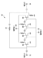
- FIG. 1 is a diagram showing a schematic configuration of a current-voltage conversion circuit of a conventional current-voltage converter (Non-Patent Document 1).
- a terminal current source
- the conversion voltage corresponding to the target current is measured at the output terminal 14.
- Signal amplification is performed using four FETs (H1 to H4), and the source output signal of H4 in the final stage is fed back to the gate of H1 on the input side to realize current-voltage conversion.
- FETs In the current-voltage conversion circuit of the prior art, generally available FETs operating at room temperature have been used.
- Non-Patent Document 1 uses a pseudomorphic high electron mobility transistor (HEMT).
- HEMT pseudomorphic high electron mobility transistor
- the present invention has been made in view of such a problem, and an object of the present invention is to provide a means for measuring a minute current with high sensitivity in an extremely low temperature state.
- one embodiment of the present invention is an amplification unit having at least three stages in which each stage is composed of electronic elements, and a target current is supplied to the first stage and the final stage.
- the electronic element includes an amplification unit that returns an output signal to the first stage and converts the target current into a voltage, and a buffer unit that is connected to the amplification unit and outputs the converted voltage.
- a field effect transistor (FET) adapted for operation at the above temperature, characterized in that the gate of the FET is connected to a ground potential and a single power source common to each of the FETs is supplied. It is a voltage converter. ..
- the following disclosure relates to a current-voltage converter that measures a minute current with high sensitivity even in an extremely low temperature state.
- the current-voltage converter of the present disclosure uses an element optimized exclusively for low-temperature operation (for example, HEMT) as an electronic element for current-voltage conversion.
- HEMT high-temperature operation
- the current-voltage conversion characteristics that are significantly superior to those of the prior art are realized.
- the power supply configuration to the current-voltage conversion circuit is simplified, the heat inflow from the outside of the cooling device is suppressed, and the load of the cooling device is reduced.
- the FETs H1 to H4 used in the current-voltage conversion circuit 10 would operate even at room temperature.
- the operating performance of electronic elements differs depending on the operating temperature, and in the case of a current-voltage conversion circuit, all characteristics such as the power supply voltage to be supplied to the FET, conversion efficiency, noise characteristics, and operating requirements change with temperature. ..
- the pseudomorphic FET of the current-voltage converter disclosed in Non-Patent Document 1 is a generally available electronic device that operates at both normal temperature and low temperature. The reason for this is that since it is possible to operate at room temperature in the inspection of electronic devices, it is possible to first perform characteristic evaluation at room temperature and then selectively and arbitrarily perform costly low temperature evaluation. From the viewpoints of test efficiency during mass production of electronic devices and ease of use / evaluation at room temperature, both suppliers and users have a great advantage in manufacturing electronic devices that operate at room temperature and low temperature. be.
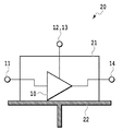
- FIG. 2 is a diagram illustrating a configuration for low temperature operation of the current-voltage converter.
- Another problem with the prior art current-voltage converters is the limited capacity of the cooling device when the current-voltage converters are used in low temperature conditions.
- the current-voltage conversion circuit 10 shown in FIG. 1 is arranged inside a cooling device including, for example, a cooling stage 22 and a case 21 thereof.
- the current-voltage conversion circuit 10 is symbolically indicated by an amplifier symbol, it may actually be a package in which a plurality of elements (FETs) and others shown in FIG. 1 are mounted on a substrate. Further, this package may be placed in a case such as oxygen-free copper and placed on the stage 22 together with the case.
- the current input terminal 11, the voltage output terminal 14, and the two power supply terminals 12 and 13 are taken out from the inside of the case 21 to the outside.
- the dilution refrigerator has a mechanism in which the above-mentioned flow voltage conversion circuit 10 is mounted in a tubular can having a diameter of 0.5 to 1 m and a height of 2 m, and helium is circulated inside the can.
- the dilution refrigerator may also include external mechanisms such as pumps and compressors for helium circulation not shown in FIG.
- diluting refrigerators about 10 mK to 1K
- 3He refrigerators about 300 mK
- 4He refrigerators about 1.5K
- liquid helium 4.2K
- Refrigerant-free pulse tube refrigerator 1.5K-300K can be used. Note that the form of the case and cooling stage varies depending on the type of cooling system.
- Cooling capacity is known as an important index of the cooling device, and indicates how many watts or less of heat is required in the cooling device to maintain a certain temperature. In other words, it means the maximum calorific value that can be tolerated by the object to be cooled in the cooling device.
- a cooling device for achieving a low temperature of about millikelvin, it is a state-of-the-art device and typically has a cooling capacity of about 500 ⁇ W at 100 mK. This means that the power consumption generated in the cooling device must be suppressed to 500 ⁇ W or less in order to maintain a low temperature of 100 mK. Therefore, the index "cooling capacity" may be larger as the temperature set by the cooling device is higher. For example, when the temperature is maintained at 200 mK, the heat generation, that is, the power consumption of the object to be cooled in the cooling device may be twice as large as that at 100 mK.
- the lower the temperature of an electronic circuit the lower the noise by suppressing thermal noise.
- Even for current-voltage converters it is advantageous to use them in an environment where the temperature is as low as possible in order to realize the ultimate low noise measurement. Therefore, it is necessary to suppress the power consumption of the current-voltage converter as much as possible and make it smaller than the index "cooling capacity" of the cooling device.
- the current-voltage converter of the prior art (Non-Patent Document 1) shown in FIG. 1 has a power consumption of 1.5 mW, and can be used only at 500 mK or more even if a state-of-the-art dilution refrigerator is used. In order to reduce the load on the cooling device, it is necessary to reduce the power consumption of the current-voltage converter and suppress the heat inflow from the outside to the cooling device.
- FIG. 3 is a diagram showing a configuration of a current-voltage conversion circuit in the current-voltage conversion device of the present disclosure.
- the current-voltage conversion circuit 100 is roughly divided into a current-voltage conversion unit 101 and an output stage source follower unit 102.
- the current-voltage conversion unit 101 has a basic amplifier configuration similar to that of FIG. 1, and includes three FETs (H1 to H3) constituting a common source voltage amplification stage and a final output stage FET (H4) which is a source follower. To be equipped.
- the output voltage 108 from the source of H4 is fed back to the gate of H1 via the feedback resistor 107.
- each FET is grounded by a gate resistor 106, and each FET is self-biased by a source resistor with a power source from a single power supply terminal 105.
- the current-voltage conversion unit 101 described above functions as an amplification unit that supplies the target current to the first stage, returns the output signal of the final stage to the first stage, and converts the target current into a voltage.
- the output stage source follower unit 102 has a configuration not found in the current-voltage conversion circuit 10 of the prior art shown in FIG. That is, in the current-voltage conversion circuit 100 of the present disclosure, the FET (H5) of the output stage source follower unit 102 is a cable when a coaxial cable for taking out a voltage output from the cooling device is connected to the rear stage side of the output voltage terminal 104. It is possible to prevent the frequency characteristics of the current-voltage conversion circuit 100 from being deteriorated due to the floating capacitance of the current / voltage conversion circuit 100.
- a source follower in a circuit output is generally used to lower the output impedance of the circuit and avoid fluctuations in the operation of the circuit itself due to connection with the next stage circuit. That is, the output stage source follower unit 102 is connected to the amplification unit and functions as a buffer unit that outputs the voltage converted from the target current.
- the power supply voltage is supplied to the gate by the self-bias method for the FETs of each amplification stage of H1 to H5. That is, the gate and ground of each FET are connected by a gate grounding resistance 106, and the gate is fixed at 0V. Since there is also resistance between the source and ground, if a voltage is supplied from the power supply terminal 105 to the drain, the source potential becomes positive. Therefore, when an n-type HEMT is used, it is equivalent to applying a negative voltage between the gate and the source. If appropriate values are selected for the gate resistance and the source resistance, an appropriate power supply voltage is supplied to each FET by a self-bias method by providing only one power supply terminal 105.
- the power supply terminal 13 for the drain and the power supply terminal 12 for the gate are independently required for the four FETs (H1 to H4). .. Therefore, it is necessary to connect the inside and outside of the cooling device shown in FIG. 2 by at least two systems of electrical wiring. The heat inflow from these two electrical wires to the cooling device was a load on the cooling device. If there are a plurality of measurement targets for minute currents, it is necessary to house a plurality of current-voltage conversion circuits in the cooling device, but the need for at least two wires is also a problem in terms of space inside the refrigerator.
- the amount of heat inflow per wiring can be estimated from the metal material used for wiring and the length of the wiring determined by the structure of the refrigerator. Copper-nickel alloys, stainless steel, superconducting wires, etc. are generally used as wiring materials at low temperatures. Although the superconducting wire has the lowest thermal conductivity, it is limited to use only at extremely low temperatures of 4K or less, so here we estimate the case of using a widely used coaxial cable of cupronickel (copper nickel alloy). View. In the case of a cable having a thickness (0.86 mm ⁇ ) that is easy to use and is generally used, the thermal conductivity is about 0.07 mW ⁇ m / K, for example.
- the amount of heat inflow per wiring is about 0.2 mW.
- the amount of heat inflow of 0.2 mW is not negligible as compared with the power consumption of 0.75 mW in the main body of the current-voltage converter.
- each FET (H1 to H5) of the current-voltage conversion circuit of FIG. 3 uses FETs having a configuration specialized for low-temperature operation.
- FETs specialized for low-temperature operation include GaAs-based HEMTs, and specifically, n-Al x Ga 1-x As / GaAs HEMTs and GaAs quantum well HEMTs. Since the GaAs-based HEMT exhibits high electron mobility at low temperatures, it operates as a wideband and noise-free FET, and it is easy to fabricate an element having a large transconductance at low temperatures.
- the HEMT (FET) used in the current-voltage conversion circuit 100 shown in FIG. 3 is a HEMT having a GaAs-AlGaAs modulated-doped superlattice structure.
- Other usable ones are pseudomorphic HEMT and InP-based HEMT. These HEMTs can operate at low temperatures and have excellent noise characteristics.
- the current-voltage converter of the present disclosure is an amplification unit 101 having at least three stages in which each stage is composed of electronic elements, the target current is supplied to the first stage, and the output signal of the final stage is returned to the first stage.
- the electronic element includes an amplification unit that converts the target current into a voltage and a buffer unit 102 that is connected to the amplification unit and outputs the converted voltage, and the electronic element is suitable for operation at a temperature of 150 K or less. It can be implemented as a field effect transistor (FET) in which the gate of the FET is connected to a ground potential and a single power source 105 common to each of the FETs is supplied.
- FET field effect transistor
- the configuration of the channel portion is related to the detection sensitivity for minute currents.
- a channel is formed between the drain and the source.
- the current in the channel is controlled by the input signal to the gate.
- the thickness d of the gate insulating layer needs to be sufficiently large in order to suppress the leakage current between the channel and the gate. Therefore, in a HEMT that can operate at both normal temperature and low temperature, the thickness d of the insulating layer is usually 100 nm or more.
- the larger the thickness d the smaller the response to the change in the gate voltage, and the lower the detection sensitivity to the input signal to the gate.
- the insulating layer thickness d is 55 nm, which is 100 nm or less, at a temperature of 4 K.
- the electrical resistance between the gate and the channel is 200 k ⁇ / mm as an actual measurement value at room temperature, and it cannot be used because the leak operation is large.
- the electrical resistance between the gate and the channel is 1 G ⁇ / mm or more, so that the leakage current can be ignored.
- GaAs-AlGaAs HEMT a Schottky barrier is formed, so that the gate and the channel are naturally insulated, but the insulating layer needs to be thickened to some extent.
- the generally available GaAs-AlGaAs HEMT configuration is disclosed in, for example, Non-Patent Document 2, and although the doping amount is not described, the thickness of the insulating layer is 210 nm. The required thickness of the insulating layer differs depending on the material, but in the case of GaAs-AlGaAs, it is generally considered that the thickness is about 100 nm or more.
- the current-voltage converter of the present disclosure adopts a configuration specialized for low-temperature operation, in which the gate insulating layer has a thickness of 100 nm or less, which cannot be selected for normal temperature operation, and is used for a current-voltage conversion circuit.
- the configuration of the HEMT specialized for low temperature operation will be further mentioned.
- the distance between the gate and the channel is short and the gate insulating layer is thin.
- the larger the change amount (transconductance) of the channel current with respect to the gate voltage is, the better, the larger the doping amount, the larger the current detection sensitivity.
- the two conditions of the gate insulating layer thickness and the doping amount can be optimized only within a range in which carriers do not occur in the gate insulating layer. It is known that if this range is exceeded, a gate leak current is generated at room temperature, and the mobility is lowered due to parallel conduction (Parallel Conduction), resulting in deterioration of HEMT characteristics. If carriers are generated in the gate insulating layer of the HEMT and a gate leak current flows, it cannot be used not only as a current-voltage conversion circuit but also as one that does not have the basic operation and performance of an electronic element at room temperature.
- HEMTs In order to ensure the basic operation of the electronic device described above, most commercially available HEMTs have a thickness of 100 nm or more as a barrier layer that is a part of the gate insulating layer, for example.
- the barrier layer is 180 nm, and the total gate thickness of the three-layer structure is 210 nm. In a HEMT having such a thick gate insulating layer, it becomes a barrier for highly sensitive measurement at a low temperature.
- the thickness of the gate insulating layer of the HEMT is 55 nm, and delta doping (6 ⁇ 10 11 cm- 2 ) is performed twice (channel carrier density 4 ⁇ 10 11 cm- 2).
- a current-voltage conversion circuit was prototyped using (corresponding to), and excellent noise performance was confirmed.
- These HEMTs have a gate resistance with an measured electrical resistance of 200 k ⁇ / mm at room temperature and cannot be used as a HEMT at room temperature due to leakage current.
- high sensitivity and low power consumption can be realized by using the above-mentioned HEMT specialized for low temperature operation at an extremely low temperature and simplifying the power supply configuration for the current-voltage conversion circuit as shown in FIG.
- the thickness of the gate insulating layer is 100 nm or less, preferably 55 nm or less, and the doping amount is equivalent to the carrier density of the channel 4 ⁇ 10 11 cm- 2. It can be said that it exceeds.
- the current-voltage converter of the present disclosure can realize a highly sensitive measurement of a minute current at an extremely low temperature.
- the present invention can be used for highly sensitive measurement of minute currents.
Landscapes
- Engineering & Computer Science (AREA)
- Power Engineering (AREA)
- Junction Field-Effect Transistors (AREA)
Abstract
従来技術の電流電圧変換装置で使用されたFETは、極低温で動作させると電流電圧変換効率が不足し、感度の良い電流測定は難しかった。外部から冷却装置内部への熱流入のために、所望の低温環境を実現できない問題もあった。極めて低温の状態であっても、感度良く微小電流を測定する電流電圧変換装置を提供する。本開示の電流電圧変換装置は、電流電圧変換のための電子素子として、低温動作専用に最適化した素子(例えばHEMT)を使用する。150K以下の低温または絶対零度近くの極低温の状態で電流電圧変換装置を動作させても、従来技術よりも格段に優れた電流電圧変換特性を実現する。電流電圧変換回路への電源およびバイアス回路を簡略化して、冷却装置の外部からの熱流入を抑えて、冷却装置の負荷を減らす。
Description
本発明は、電流を電圧に変換する電子回路に関する。
電流を測定するために、対象となる電流を電圧に変換し、電圧計を用いて電流を計測することが知られている。微小な電流を正確に読み出すためには、低ノイズの電子回路を用いて電流を電圧に変換する必要がある。これを実現するために、電流電圧変換装置を低温で用いて熱ノイズを低減する手法が利用されている。超長波~短波帯域(1kHz~30MHz)の電流信号に対しては、低温動作する低消費電力電界効果トランジスタ(FET)を用いた電流電圧変換装置が報告されている(非特許文献1)。
図1は、従来技術の電流電圧変換装置の電流電圧変換回路の概略構成を示す図である(非特許文献1)。電流電圧変換回路10では、入力端子11に測定する対象の電流が流れ出す端子(電流ソース)を接続し、出力端子14において、対象電流に対応した変換電圧の測定を行う。4つのFET(H1~H4)を用いて信号増幅を行い、最終段のH4のソース出力信号を入力側のH1のゲートにフィードバックすることで電流-電圧変換を実現する。従来技術の電流電圧変換回路では、一般に入手可能な室温動作するFETが使用されてきた。例えば非特許文献1の電流電圧変換装置は、シュードモルフィック高電子移動度トランジスタ(HEMT:High Electron Mobility Transistor)を用いている。
橋坂他, "Cross-correlation measurement of quantum shot noise using homemade transimpedance amplifiers, 2014年, Rev. Sci. Instrum. 85, 054704 PAM-XIAMEN社 GaAs HEMT Epi wafer 製品カタログページ、[online]令和2年3月6日検索、インターネット<URL:https://www.powerwaywafer.com/gaas-hemt-epi-wafer.html>
橋坂他, "Cross-correlation measurement of quantum shot noise using homemade transimpedance amplifiers, 2014年, Rev. Sci. Instrum. 85, 054704 PAM-XIAMEN社 GaAs HEMT Epi wafer 製品カタログページ、[online]令和2年3月6日検索、インターネット<URL:https://www.powerwaywafer.com/gaas-hemt-epi-wafer.html>
しかしながら、従来技術の室温動作可能なFETを使用した電流電圧変換装置では、信号増幅部が持つ開ループ利得が十分でない問題があった。電流電圧変換装置において、例えば宇宙線や量子デバイス信号、電流の「量子的な揺らぎ」の測定、低温での物理現象の観測等をする場合は、非常に小さな信号を測定することになる。このような微小電流の測定のためには、最低でも液体窒素の温度(77K)から絶対零度近くの非常に低温にして、電流電圧変換装置を動作させる必要がある。従来技術の電流電圧変換装置で使用されていたFETは、室温および低温で動作することを前提としている。このため、極低温でこのFETを動作させても、電流電圧変換効率が不足し、感度の良い電流測定は難しかった。さらに、冷却状態で使用する際の電流電圧変換装置の消費電力や外部からの熱流入により、冷却装置で所望の低温環境を実現できない問題もあった。
本発明はこのような問題に鑑みてなされたものであって、その目的とするところは、極めて低温の状態で感度良く微小電流を測定する手段を提供することにある。
このような目的を達成するために、本発明の1つの実施態様は、各段が電子素子で構成された少なくとも3段を有する増幅部であって、初段に対象電流が供給され、最終段の出力信号を前記初段へ帰還し、前記対象電流を電圧に変換する、増幅部と、前記増幅部に接続され、前記変換された電圧を出力するバッファ部とを備え、前記電子素子は、150K以下の温度における動作に適合された電界効果トランジスタ(FET)であって、前記FETのゲートが接地電位に接続され、前記FETの各々に共通する単一の電源が供給されることを特徴とする電流電圧変換装置である。
極めて低温の状態で、感度良く微小電流を測定する手段を提供する。
以下の開示は、極めて低温の状態であっても、感度良く微小電流を測定する電流電圧変換装置に関する。本開示の電流電圧変換装置は、電流電圧変換のための電子素子として、低温動作専用に最適化した素子(例えばHEMT)を使用する。これにより、150K以下の低温または絶対零度近くの極低温の状態で電流電圧変換装置を動作させても、従来技術よりも格段に優れた電流電圧変換特性を実現する。さらに、電流電圧変換回路への電源構成を簡略化して、冷却装置の外部からの熱流入を抑え、冷却装置の負荷を減らす。
再び図1を参照すると、電流電圧変換回路10で使用されるH1~H4のFETは、それぞれ室温でも動作することを前提としていた。一般に、電子素子はその使用温度によって動作性能が異なり、電流電圧変換回路であれば、FETへ供給すべき電源電圧や、変換効率、ノイズ特性などの全て特性、動作要件が温度と伴に変化する。例えば非特許文献1で開示された電流電圧変換装置のシュードモルフィックFETは、一般に入手できる電子デバイスであって、常温および低温のどちらでも動作するものを用いている。この理由は、電子素子の検査において常温で動作できることで、まず常温で特性評価を行って、コストの掛かる低温評価を選択的、任意的に実施できるからである。電子素子の量産時の試験の効率、常温時での使用・評価の容易さなどの観点から、供給者および使用者の両方にとって、常温および低温で動作する電子素子を作製することに大きなメリットがある。
しかしながら、宇宙線や量子デバイス信号、電流の「量子的な揺らぎ」などのような微小電流を測定するため絶対零度近くまでFETを冷却する状況では、常温および低温の両方で動作するFETの電流電圧変換特性は不十分なものであった。発明者らは、従来技術の電流電圧変換装置で使用されていた電子素子を、低温での動作および性能に特化したものにすれば、低温状態においてより好ましい低雑音特性が得られるのではないかとの着想に至った。
図2は、電流電圧変換装置の低温動作のための構成を説明する図である。従来技術の電流電圧変換装置におけるもう1つの問題は、電流電圧変換装置を低温状態で使用する場合の、冷却装置の能力による制限である。図2の電流電圧変換装置20において、図1に示した電流電圧変換回路10は、例えば冷却ステージ22およびそのケース21からなる冷却装置の内部に配置されている。電流電圧変換回路10は、増幅器の記号でシンボル的に示しているが、実際には図1に示した複数の素子(FET)他が基板上に実装されたパッケージ状のものであり得る。さらに、このパッケージを無酸素銅等のケースに入れ、ケースごとステージ22に配置したものであり得る。ケース21の内部から外部へ、電流入力端子11、電圧出力端子14、2つの電源供給端子12、13が取り出される。
冷却装置は様々な形態ものがあり得るが、一例を挙げれば、希釈冷凍機を使用できる。希釈冷凍機は直径0.5~1m×高さ2mほどの筒状の缶の中に上記の流電圧変換回路10を実装して、缶の内部でヘリウムを循環させる機構を持つ。希釈冷凍機は、図2には示していないヘリウム循環のためのポンプやコンプレッサ等の外部機構も含み得る。他のタイプの冷却装置と冷却温度を例示すれば、希釈冷凍機:10mK~1K程度、3He冷凍機:300mK程度、4He冷凍機:1.5K程度、液体ヘリウム:4.2K、液体窒素:77K、無冷媒パルスチューブ冷凍機:1.5K~300Kを利用できる。冷却装置のタイプに応じて、ケースおよび冷却ステージの形態は変わることに留意されたい。
電流電圧変換回路によって高感度で微小電流を測定するためには、図2のように冷却装置と組み合わせて用いることが前提となる。上述の冷却装置では、その冷却能力が有限であるため、内部に配置する電流電圧変換装置10の消費電力を低く保つ必要がある。同時に、外部から冷却装置内へ流入する熱を最小に抑える必要がある。最先端の冷却装置であっても、その内部に消費電力の大きな電子回路を収めたり、外部から冷却装置への熱流入が多かったりすれば、極低温に保つことは難しくなる。
冷却装置の重要な指標として「冷却能力」が知られており、ある温度を維持するために冷却装置内における発熱が何ワット以下の必要があるかを示す。言い換えると、冷却装置内における冷却対象に許容できる最大発熱量を意味する。例えばミリケルビン程度の低温を実現するための冷却装置(希釈冷凍機)の場合、最先端の装置で、冷却能力は500μW at100mK程度が典型的である。これは100mKの低温を維持するためには冷却装置内で生じる消費電力を500μW以下に抑えなければならないことを意味する。したがって指標「冷却能力」は、冷却装置によって設定する温度が高いほど大きくて良い。例えば200mKの温度に維持する場合は、100mKとする場合と比べて、冷却装置内における冷却対象の発熱すなわち消費電力が2倍大きくて良いことになる。
一般に電子回路は、その温度が低ければ低いほど、熱雑音を抑制して低ノイズにできる。電流電圧変換装置でも、できるだけ温度の低い環境で使うのが究極的な低雑音測定の実現に向け有利である。したがって、電流電圧変換装置の消費電力をできるだけ抑制し、冷却装置の指標「冷却能力」に対して小さくする必要がある。図1に示した従来技術(非特許文献1)の電流電圧変換装置は消費電力が1.5mWであり、最先端の希釈冷凍機を用いても500mK以上でしか使用できなかった。冷却装置への負荷を減らすためには、電流電圧変換装置の消費電力を減らし、外部から冷却装置への熱流入を抑える必要がある。
本開示の電流電圧変換装置では、低温動作に特化して構成された電子素子(FET)を用いること、および、電流電圧変換回路の特有の構成によって、上述の低温動作時の開ループ利得の不足、冷却装置の能力の制限の問題を同時に解決する。
図3は、本開示の電流電圧変換装置における電流電圧変換回路の構成を示す図である。電流電圧変換回路100は、大きく分けて電流電圧変換部101と、出力段ソースフォロア部102とを含む。電流電圧変換部101は、基本的な増幅器構成としては図1と類似しており、コモンソース電圧増幅段を構成する3つのFET(H1~H3)およびソースフォロアである最終出力段FET(H4)を備える。H4のソースからの出力電圧108を、フィードバック抵抗107を介してH1のゲートへ帰還させている。各FETへのゲートは、ゲート抵抗106によって接地電位とされ、各FETは単一の電源供給端子105からの電源によりソース抵抗によって自己バイアスされる。上述の電流電圧変換部101は、初段に対象電流が供給され、最終段の出力信号を初段へ帰還し、対象電流を電圧に変換する、増幅部として機能する。
出力段ソースフォロア部102は、図1の従来技術の電流電圧変換回路10には無い構成である。すなわち本開示の電流電圧変換回路100では、出力段ソースフォロア部102のFET(H5)は、出力電圧端子104の後段側に冷却装置から電圧出力を取り出すための同軸ケーブルを接続する場合に、ケーブルの浮遊容量により電流電圧変換回路100の周波数特性が悪化するのを防ぐ。一般に回路出力におけるソースフォロアは、その回路の出力インピーダンスを下げ、次段回路との接続によって受けるその回路自身の動作の変動を避けるために使用される。すなわち、出力段ソースフォロア部102は、増幅部に接続され、対象電流から変換された電圧を出力するバッファ部として機能する。
消費電流の制限がない常温における電流測定時には、電流電圧変換部101のソースフォロア(H4)に大きな電流を流すことができる。しかしながら、冷却装置の使用を前提として極低温において電流電圧変換装置を使用する場合には、1段構成のソースフォロアだけでは不十分と判った。ソースフォロアのFETに割り当てることのできる消費電力には制限があり、ソースフォロアの出力インピーダンスを十分に下げることができない。そこで出力段ソースフォロア部102をさらに備えることで、後段側のケーブル浮遊容量による電流電圧変換特性の周波数特性悪化を防ぐことができる。後述する低温動作に特化された低電流のFETを使用することで、電流電圧変換回路全体でも、増幅段の数の増加(4→5段)を補ってより小さい消費電流を実現できる。このため、極低温測定における冷却装置への負荷を軽減し、同時に広帯域の微小電流測定を実現する。
本開示の電流電圧変換装置において特徴的な点の1つは、H1~H5の各増幅段のFETに対して自己バイアス方式でゲートに電源電圧を供給している点にある。すなわち、各FETのゲートとグランドの間をゲート接地抵抗106によって接続し、ゲートは0Vに固定される。ソースとグランド間にも抵抗があるため、電源供給端子105からドレインに電圧を供給すれば、ソース電位はプラスとなる。したがって、n型のHEMTを使用する場合には、ゲート-ソース間に負電圧を印可したのと等価になる。ゲート抵抗およびソース抵抗に適切な値を選べば、1つの電源供給端子105を備えるだけで各FETに対して自己バイアス方式で適切な電源電圧が供給される。
図1に示した従来技術の電流電圧変換回路10では、4つのFET(H1~H4)に対して、ドレイン用の電源供給端子13と、ゲート用の電源供給端子12が独立に必要であった。このため、図2に示した冷却装置の内外を少なくとも2系統の電気配線によって接続する必要があった。この2本の電気配線から冷却装置への熱流入が、冷却装置の負荷となっていた。複数の微小電流の測定対象があれば、複数の電流電圧変換回路を冷却装置に収納する必要があるが、配線が少なくとも2本必要なことは、冷凍機内のスペースの点でも問題であった。
配線に用いる金属材料、および、冷凍機の構造から決まる配線の長さから、配線1本あたりの熱流入量を見積もることができる。配線の材料として低温で一般に用いられるのは、銅ニッケル合金、ステンレス、超電導線などである。超電導線は最も熱伝導度が小さいものの、4K以下の極低温でのみの使用に限られるので、ここでは広く用いられているキュプロニッケル(銅ニッケル合金)の同軸ケーブルを用いた場合を試算してみる。使いやすく一般に用いられている太さ(0.86mmφ)のケーブルの場合、一例を挙げれば、熱伝導度は約0.07mW・m/K である。4Kまで冷却するものとして、標準的な冷却装置のサイズを例に1mの配線を用いたとすると、配線1本あたりの熱流入量は約0.2mWとなる。0.2mWの熱流入量は、電流電圧変換装置本体における消費電力0.75mWに比べて無視できないほど大きい。
これに対して、図3の本開示の電流電圧変換回路100によれば、電源配線は1本のみで済むため、電気配線を経由して外部からら冷却装置内へ流入する熱を半分程度に抑えることができる。重要な指標「冷却能力」の観点からも、冷却装置の負荷を減らすことができるのは明らかである。さらに冷却装置内に複数個の電流電圧変換装置を収納する場合でも、配線スペースおよび熱の流入の抑制の効果がある。
本開示の電流電圧変換装置においてもう1つの特徴的な点は、図3の電流電圧変換回路の各FET(H1~H5)について、低温動作に特化した構成のFETを使用していることにある。低温動作に特化したFETの例としてGaAs系HEMTがあり、具体的には、n-AlxGa1-xAs/GaAs HEMT、GaAs量子井戸HEMTがある。GaAs系HEMTは低温で高い電子移動度を示すことから、広帯域かつノイズの少ないFETとして動作し、低温でトランスコンダクタンスの大きな素子の作製も容易である。
従来技術の電流電圧変換装置で使用されていた常温および低温の両方で動作するFETと、本開示の電流電圧変換装置で使用した低温動作に特化したFETの特性について、より具体的に述べておく。図3に示した電流電圧変換回路100で使用したHEMT(FET)は、GaAs-AlGaAs変調ドープ超格子構造を持つHEMTである。他に使用可能なものとしては、シュードモルフィックHEMT、InP系HEMTがある。これらのHEMTは低温で動作可能で、優れた雑音特性を持つ。
したがって、本開示の電流電圧変換装置は、各段が電子素子で構成された少なくとも3段を有する増幅部101であって、初段に対象電流が供給され、最終段の出力信号を前記初段へ帰還し、前記対象電流を電圧に変換する、増幅部と、前記増幅部に接続され、前記変換された電圧を出力するバッファ部102とを備え、前記電子素子は、150K以下の温度における動作に適合された電界効果トランジスタ(FET)であって、前記FETのゲートが接地電位に接続され、前記FETの各々に共通する単一の電源105が供給されるものとして実施できる。
HEMTでは、チャネル部分の構成が微小電流に対する検出感度に関係している。HEMTの断面構造を考えると、ドレインおよびソースの間にチャネルが形成される。チャネルにおける電流は、ゲートへの入力信号によって制御される。常温で動作するHEMTの場合は、チャネルとゲート間のリーク電流を抑えるために、ゲート絶縁層の厚さdは十分に大きい必要がある。したがって、常温および低温の両方で動作可能なHEMTは、絶縁層の厚さdは通常100nm以上ある。一方で、厚さdが大きいほど、ゲート電圧の変化に対する応答が小さくなり、ゲートへの入力信号に対する検出感度が低下する。
本開示の電流電圧変換装置で使用した低温動作に特化したチャネル幅3mmのGaAs-AlGaAsHEMTでは、温度4Kで絶縁層厚さdは、100nm以下の55nmとした。このHEMTを増幅素子として利用する場合、室温ではゲート-チャネル間の電気抵抗は実測値で200kΩ/mmとなって、リーク動作が大きいため使用できない。一方で、例えば液体ヘリウム温度(4.2K)ではゲート-チャネル間の電気抵抗は1GΩ/mm以上のため、リーク電流を無視できる。常温における正常な動作を諦めて、低温動作に特化したHEMTを使用することで、極低温用の電流電圧変換回路としてHEMTの電流検出感度を大きく向上させることができる。
一般に常温動作のHEMTでは、ゲート-チャネル間のリークを抑えることが重要である。GaAs-AlGaAs HEMTでは、ショットキー障壁ができるため、ゲートとチャンネルは自然に絶縁されるものの、絶縁層はある程度厚くする必要がある。一般に入手可能なGaAs-AlGaAs HEMTの構成は、例えば非特許文献2に開示されており、ドープ量について記載はないが、絶縁層の厚さは210nmとなっている。材料が違えば絶縁層の必要な厚さも異なるが、GaAs-AlGaAsの場合は概ね100nm以上の厚さが一般的だと考えられる。本開示の電流電圧変換装置では、常温動作をさせるためには選択し得ない、ゲート絶縁層が100nm以下の厚さを持つ、低温動作に特化した構成を採用し、電流電圧変換回路への電源構成を簡略化して、従来技術よりも格段に優れた電流電圧変換特性を実現した。
ここで、低温動作に特化したHEMTの構成についてさらに言及しておく。上述のように、電流電圧変換回路において、電流検出感度を大きくするためにはゲートとチャネルの距離が近く、ゲート絶縁層が薄いほど良い。また、ゲート電圧に対するチャンネル電流の変化量(トランスコンダクタンス)が大きいほど良いので、ドープ量は多いほど電流検出感度が大きくなる。
しかしながら、ゲート絶縁層厚さおよびドープ量の2つの条件は、ゲート絶縁層にキャリアが生じないような範囲でしか最適化できない。この範囲を超えると、室温ではゲートリーク電流が生じたり、平行伝導(Parallel Conduction)によって移動度が低下しHEMTの特性が劣化したりすることが知られている。HEMTのゲート絶縁層でキャリアが生じ、ゲートリーク電流が流れれば、電流電圧変換回路としてはもちろん、常温で電子素子の基本動作・性能を持たないものとして使用できなくなる。
上述の電子素子としての基本的な動作を確保するために、市販のHEMTは、例えばゲート絶縁層の一部であるバリア層として100nm以上の厚さを持つものが大半である。非特許文献2によれば、バリア層は180nmであり、3層構造のゲート全厚さは210nmである。このような厚いゲート絶縁層を持つ構成のHEMTでは、低温で高感度な測定を行う障壁となる。
本開示の電流電圧変換装置では、HEMTのゲート絶縁層の厚さを55nmとして、2回のデルタドープ(6×1011cm-2)を行ったもの(チャンネルのキャリア密度4×1011cm-2に相当)を使用して、電流電圧変換回路を試作し、優れた雑音性能を確認した。これらのHEMTは、室温で電気抵抗の実測値が200kΩ/mmのゲート抵抗を持ち、リーク電流のために室温ではHEMTとして用いることができない。しかしながら、上述の低温動作に特化したHEMTを極めて低温で使用し、図3に示したように電流電圧変換回路への電源構成を簡略化することで、高感度で低消費電力を実現できる。低温動作に特化したHEMTの構成の目安としては、ゲート絶縁層の厚さが100nm以下であって好ましくは55nm以下であって、かつドープ量はチャンネルのキャリア密度4×1011cm-2相当を越えるものであると言える。
以上詳細に述べたように、本開示の電流電圧変換装置によって、極めて低温の状態で感度良い微小電流の測定を実現できる。
本発明は、微小電流の高感度な測定に利用することができる。
10、100 電流電圧変換回路
11、103 電流入力端子
12、13、105 電源端子
14、104 電圧出力端子
15、107 帰還抵抗
20 電流電圧変換装置
21 ケース
22 冷却ステージ
108 ドレイン出力電圧
11、103 電流入力端子
12、13、105 電源端子
14、104 電圧出力端子
15、107 帰還抵抗
20 電流電圧変換装置
21 ケース
22 冷却ステージ
108 ドレイン出力電圧
Claims (5)
- 各段が電子素子で構成された少なくとも3段を有する増幅部であって、初段に対象電流が供給され、最終段の出力信号を前記初段へ帰還し、前記対象電流を電圧に変換する、増幅部と、
前記増幅部に接続され、前記変換された電圧を出力するバッファ部と
を備え、
前記電子素子は、150K以下の温度における動作に適合された電界効果トランジスタ(FET)であって、前記FETのゲートが接地電位に接続され、前記FETの各々に共通する単一の電源が供給されることを特徴とする電流電圧変換装置。 - 前記増幅部は4段のコモンソース電圧増幅段であって、最終段はソースフォロアを構成し、
前記バッファ部は、前記電子素子で構成されたソースフォロアであることを特徴とする請求項1に記載の電流電圧変換装置。 - 前記FETは、高電子移動度トランジスタ(HEMT)であって、ゲート絶縁層厚さが100nm以下であることを特徴とする請求項1または2に記載の電流電圧変換装置。
- 前記HEMTは、GaAs-AlGaAs変調ドープ超格子構造のHEMT、シュードモルフィックHEMT、またはInP系HEMTのいずれかであることを特徴とする請求項3に記載の電流電圧変換装置。
- 冷却装置内に請求項1乃至4いずれかの電流電圧変換装置を備えた微小電流測定装置。
Priority Applications (3)
| Application Number | Priority Date | Filing Date | Title |
|---|---|---|---|
| JP2022507943A JPWO2021186652A1 (ja) | 2020-03-18 | 2020-03-18 | |
| PCT/JP2020/012150 WO2021186652A1 (ja) | 2020-03-18 | 2020-03-18 | 電流電圧変換装置 |
| US17/911,019 US20230120951A1 (en) | 2020-03-18 | 2020-03-18 | Voltage Current Conversion Device |
Applications Claiming Priority (1)
| Application Number | Priority Date | Filing Date | Title |
|---|---|---|---|
| PCT/JP2020/012150 WO2021186652A1 (ja) | 2020-03-18 | 2020-03-18 | 電流電圧変換装置 |
Publications (1)
| Publication Number | Publication Date |
|---|---|
| WO2021186652A1 true WO2021186652A1 (ja) | 2021-09-23 |
Family
ID=77768407
Family Applications (1)
| Application Number | Title | Priority Date | Filing Date |
|---|---|---|---|
| PCT/JP2020/012150 Ceased WO2021186652A1 (ja) | 2020-03-18 | 2020-03-18 | 電流電圧変換装置 |
Country Status (3)
| Country | Link |
|---|---|
| US (1) | US20230120951A1 (ja) |
| JP (1) | JPWO2021186652A1 (ja) |
| WO (1) | WO2021186652A1 (ja) |
Families Citing this family (1)
| Publication number | Priority date | Publication date | Assignee | Title |
|---|---|---|---|---|
| JPWO2021186653A1 (ja) * | 2020-03-18 | 2021-09-23 |
Citations (6)
| Publication number | Priority date | Publication date | Assignee | Title |
|---|---|---|---|---|
| JPS60140907A (ja) * | 1983-12-28 | 1985-07-25 | Matsushita Electric Ind Co Ltd | 半導体集積回路 |
| JPH036029A (ja) * | 1989-06-02 | 1991-01-11 | Sharp Corp | 変調ドープヘテロ接合電界効果トランジスタ |
| JPH04107004A (ja) * | 1990-08-28 | 1992-04-08 | Fujitsu Ltd | 光受信用極低雑音フロントエンド |
| JP2009010910A (ja) * | 2007-02-23 | 2009-01-15 | Ntt Docomo Inc | 低温受信増幅器および増幅方法 |
| JP2010506397A (ja) * | 2006-10-04 | 2010-02-25 | セレックス システミ インテグラティ エッセ. ピ. ア. | 単一電圧供給型シュードモルフィック高電子移動度トランジスタ(phemt)パワーデバイスおよびこれの製造方法 |
| JP2015050464A (ja) * | 2013-09-03 | 2015-03-16 | トライクイント・セミコンダクター・インコーポレイテッドTriQuint Semiconductor,Inc. | リニア高電子移動度トランジスタ |
Family Cites Families (5)
| Publication number | Priority date | Publication date | Assignee | Title |
|---|---|---|---|---|
| JPH01192207A (ja) * | 1988-01-27 | 1989-08-02 | Nec Corp | 光受信回路 |
| JPH08162859A (ja) * | 1994-11-29 | 1996-06-21 | Hitachi Ltd | 多段増幅器 |
| JPH1065459A (ja) * | 1996-08-22 | 1998-03-06 | Fujitsu Ltd | 電流−電圧変換回路 |
| EP1962418B1 (en) * | 2007-02-23 | 2011-06-29 | NTT DoCoMo, Inc. | Cryogenic receiving amplifier and amplifying method |
| US12009414B2 (en) * | 2021-12-03 | 2024-06-11 | International Business Machines Corporation | Superconductor gate semiconductor field-effect transistor |
-
2020
- 2020-03-18 JP JP2022507943A patent/JPWO2021186652A1/ja active Pending
- 2020-03-18 US US17/911,019 patent/US20230120951A1/en not_active Abandoned
- 2020-03-18 WO PCT/JP2020/012150 patent/WO2021186652A1/ja not_active Ceased
Patent Citations (6)
| Publication number | Priority date | Publication date | Assignee | Title |
|---|---|---|---|---|
| JPS60140907A (ja) * | 1983-12-28 | 1985-07-25 | Matsushita Electric Ind Co Ltd | 半導体集積回路 |
| JPH036029A (ja) * | 1989-06-02 | 1991-01-11 | Sharp Corp | 変調ドープヘテロ接合電界効果トランジスタ |
| JPH04107004A (ja) * | 1990-08-28 | 1992-04-08 | Fujitsu Ltd | 光受信用極低雑音フロントエンド |
| JP2010506397A (ja) * | 2006-10-04 | 2010-02-25 | セレックス システミ インテグラティ エッセ. ピ. ア. | 単一電圧供給型シュードモルフィック高電子移動度トランジスタ(phemt)パワーデバイスおよびこれの製造方法 |
| JP2009010910A (ja) * | 2007-02-23 | 2009-01-15 | Ntt Docomo Inc | 低温受信増幅器および増幅方法 |
| JP2015050464A (ja) * | 2013-09-03 | 2015-03-16 | トライクイント・セミコンダクター・インコーポレイテッドTriQuint Semiconductor,Inc. | リニア高電子移動度トランジスタ |
Also Published As
| Publication number | Publication date |
|---|---|
| US20230120951A1 (en) | 2023-04-20 |
| JPWO2021186652A1 (ja) | 2021-09-23 |
Similar Documents
| Publication | Publication Date | Title |
|---|---|---|
| Incandela et al. | Characterization and compact modeling of nanometer CMOS transistors at deep-cryogenic temperatures | |
| Le Guevel et al. | Low-power transimpedance amplifier for cryogenic integration with quantum devices | |
| EP2476005B1 (en) | Squid with a coil inductively coupled to the squid via a mutual inductance | |
| Xie et al. | NbN-gated GaN transistor technology for applications in quantum computing systems | |
| Huizinga et al. | Integrated cryo-CMOS temperature sensors for quantum control ICs | |
| WO2021186651A1 (ja) | 電流電圧変換装置 | |
| Okcan et al. | A cryogenic analog to digital converter operating from 300 K down to 4.4 K | |
| Lee | A low‐power‐dissipation broadband cryogenic preamplifier utilizing GaAs MESFETs in parallel | |
| US20230120951A1 (en) | Voltage Current Conversion Device | |
| Aja et al. | Cryogenic low-noise mHEMT-based MMIC amplifiers for 4–12 GHz band | |
| WO2021186653A1 (ja) | 電流電圧変換装置 | |
| Ardizzi | Self-heating of HEMT low-noise amplifiers in liquid cryogenic environments and the limits of microwave noise performance | |
| Novikov et al. | Cryogenic low-noise amplifiers for measurements with superconducting detectors | |
| Kiviranta | Class-B cable-driving SQUID amplifier | |
| Qu et al. | 6-7 GHz cryogenic low-noise mHEMT-based amplifier for quantum computing | |
| Elad et al. | Germanium FET--A Novel Low-Noise Active device | |
| Ko et al. | Expanding scanning frequency range of Josephson parametric amplifier axion haloscope readout with Schottky diode bias circuit | |
| Alessandrello et al. | A front-end for an array of/spl mu/-bolometers for the study of the neutrino mass | |
| Limacher et al. | 4-12 GHz InP HEMT-based MMIC low-noise amplifier | |
| Valdez-Sandoval et al. | GFET dynamic performance at 77 K and circuit design proposals suitable for low-temperature microwave applications | |
| Yamamori et al. | Reliable packaging of Josephson voltage standard circuit for cryocooler operation | |
| RU2850000C1 (ru) | Криогенный сверхвысокочастотный малошумящий усилитель 3-8 ГГц на SiGe транзисторах | |
| Taub et al. | Cryogenic probe station for use in automated microwave and noise figure measurements | |
| US20250155295A1 (en) | Coulomb blockade thermometer | |
| Alekhya et al. | Efficient Dynamic VLSI Design with Error Detection and 8-Way Power Amplifier for Triple-Gate Vertical Power MOSFET |
Legal Events
| Date | Code | Title | Description |
|---|---|---|---|
| 121 | Ep: the epo has been informed by wipo that ep was designated in this application |
Ref document number: 20925765 Country of ref document: EP Kind code of ref document: A1 |
|
| ENP | Entry into the national phase |
Ref document number: 2022507943 Country of ref document: JP Kind code of ref document: A |
|
| NENP | Non-entry into the national phase |
Ref country code: DE |
|
| 122 | Ep: pct application non-entry in european phase |
Ref document number: 20925765 Country of ref document: EP Kind code of ref document: A1 |