WO2021186596A1 - アンテナ装置 - Google Patents
アンテナ装置 Download PDFInfo
- Publication number
- WO2021186596A1 WO2021186596A1 PCT/JP2020/011863 JP2020011863W WO2021186596A1 WO 2021186596 A1 WO2021186596 A1 WO 2021186596A1 JP 2020011863 W JP2020011863 W JP 2020011863W WO 2021186596 A1 WO2021186596 A1 WO 2021186596A1
- Authority
- WO
- WIPO (PCT)
- Prior art keywords
- feeding
- antenna
- substrate
- board
- antenna device
- Prior art date
Links
Images


Classifications
-
- H—ELECTRICITY
- H01—ELECTRIC ELEMENTS
- H01Q—ANTENNAS, i.e. RADIO AERIALS
- H01Q13/00—Waveguide horns or mouths; Slot antennas; Leaky-waveguide antennas; Equivalent structures causing radiation along the transmission path of a guided wave
- H01Q13/08—Radiating ends of two-conductor microwave transmission lines, e.g. of coaxial lines, of microstrip lines
Definitions
- This disclosure relates to an antenna device.
- the probe power supply has a space-saving power supply structure as compared with the method of power supply by electromagnetic coupling using a slot. Therefore, it is suitable for multipoint feeding of a single patch element in applications of orthogonal dipolarization, circular polarization, or low cross polarization of signals.
- the antenna substrate is thickened in order to widen the frequency band used in the antenna device that feeds the probe. As the antenna substrate becomes thicker, the probe becomes longer by that amount, so that the inductance component becomes larger, and there is a possibility that the inductance matching between the patch element and the feeding circuit cannot be obtained.
- Non-Patent Document 1 describes a technique of forming a conductor land at the tip of a probe and compensating for an inductance component of the probe by a capacitance component generated between the patch element and the conductor land.
- Non-Patent Document 1 it is necessary to form a through hole for electrically connecting the patch element provided on the antenna board and the feeding board. Therefore, the antenna board is stacked on the feeding board in multiple layers. is required.
- the multilayer substrate may warp. Therefore, in the conventional antenna device, when the antenna board is made thicker than the feeding board in order to widen the frequency band used, the surface of the feeding board opposite to the antenna board side has the same thickness as the antenna board. It is necessary to further provide the antenna, and there is a problem that the thickness of the entire substrate is increased.
- the present disclosure solves the above problems, and an object of the present disclosure is to obtain an antenna device capable of reducing an increase in the thickness of the entire substrate.
- the antenna device includes a flat-plate antenna substrate, one or more radiation conductors provided on the antenna substrate, and a first feeding conductor provided on a main surface of the antenna substrate opposite to the radiation conductor. And a flat plate-shaped power supply board provided with a power supply unit for feeding a signal transmitted to the antenna board side, and a through hole that electrically connects the radiation conductor and the first power supply conductor through the antenna board.
- a second feeding conductor provided on the main surface of the feeding board on the antenna board side and an intermediate board provided between the antenna board and the feeding board are provided, and the first feeding conductor and the second feeding conductor are provided. And are capacitively bonded with the intermediate substrate in between.
- the antenna board and the feeding board are capacitively coupled. Even if the through hole provided between the two is divided in the middle, the probe can be fed from the feeding board to the antenna board. Since the thickness of the antenna board and the feeding board can be multi-layered so as to be substantially symmetrical in the layer thickness direction with the intermediate board as a reference, the surface of the feeding board opposite to the side on which the antenna board is provided is provided. It is not necessary to provide a substrate having the same thickness as the antenna substrate. Thereby, in the antenna device according to the present disclosure, it is possible to reduce the increase in the thickness of the entire substrate.
- FIG. 5 is a side perspective view showing the antenna device of FIG. 4 in which a positional deviation occurs between the antenna substrate and the feeding substrate.
- FIG. 6A is a Smith chart diagram showing the input impedance of a single patch element in the antenna device of FIG. 1 before and after a positional shift occurs between the antenna board and the feeding board
- FIG. 6B is a Smith chart diagram of the antenna board and the feeding board.
- FIG. 10A is a Smith chart diagram showing the input impedance of a single patch element in the antenna device of FIG. 4 before and after a positional shift occurs between the antenna board and the feeding board
- FIG. 10B shows the antenna board and the feeding board.
- FIG. It is a Smith chart figure which shows the input impedance of a single patch element in the antenna device of FIG. It is a side perspective view which shows the antenna device which concerns on Embodiment 4.
- FIG. It is a top view which shows the antenna device of FIG. It is a side perspective view which shows the modification of the antenna device of FIG. It is a top view which shows the antenna device of FIG. It is a top view which shows the example of the feeding conductor of the antenna substrate in the antenna device of FIG. It is a top view which shows the example of the feeding conductor of the feeding board in the antenna device of FIG. It is a top view which shows the example of the feeding conductor of the antenna substrate in the antenna device of FIG.
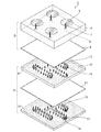
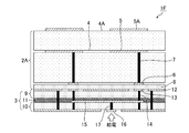
- FIG. 1 is a side perspective view showing the antenna device 1 according to the first embodiment.
- FIG. 2 is an exploded perspective view showing a substrate of each layer in the antenna device 1 of FIG.
- the antenna device 1 is a 4-element array antenna having four patch elements 5, and a signal is transmitted to an antenna substrate 2 that radiates a signal radio wave into space through the patch element 5 and an antenna substrate 2.
- a power supply board 3 for supplying power is provided.
- the patch element 5 is, for example, a circular radiation conductor, and functions as a radiation element that emits radio waves.
- the antenna substrate 2 is composed of a flat plate-shaped dielectric substrate 4, and a patch element 5 is provided on the main surface of the dielectric substrate 4, and the main surface of the dielectric substrate 4 is opposite to the patch element 5.
- the circular feeding conductor 6 is a first feeding conductor provided at a position facing the patch element 5 via the dielectric substrate 4.
- the patch element 5 and the feeding conductor 6 are electrically connected by a through hole 7.
- the through hole 7 is a probe that supplies a signal to the patch element 5.
- the antenna substrate 2 is provided with a flat plate-shaped dielectric 8 which is an intermediate substrate on the main surface on the power feeding substrate 3 side.
- the power supply substrate 3 is a multilayer substrate in which a substrate 9 and a substrate 10 having substantially the same thickness are bonded by an adhesive layer 11.
- a main plate 12 and a feeding conductor 13 are provided on the main surface of the feeding board 3 on the antenna board 2 side.
- the circular feeding conductor 13 is a second feeding conductor electrically connected to the 4-distribution synthesis circuit 15 by the vertical feeding portion 14, and is provided so as not to be electrically connected to the main plate 12.
- the 4-distribution synthesis circuit 15 is composed of triplate lines.
- the power feeding unit 16 is provided on the main surface of the power feeding board 3 on the side opposite to the antenna board 2.
- the 4-distribution synthesis circuit 15 and the feeding unit 16 are electrically connected by a vertical feeding unit 17.
- the feeding conductor 6 and the feeding conductor 13 are not in physical contact with each other due to the dielectric 8.
- the signal input to the feeding unit 16 is fed to the feeding conductor 13 by propagating through the vertical feeding unit 17, the 4-distribution synthesis circuit 15 and the vertical feeding unit 14.
- the feeding conductor 6 and the feeding conductor 13 are capacitively coupled with the dielectric 8 interposed therebetween.
- the signal propagated to the feeding conductor 13 is propagated to the feeding conductor 6 and fed to the patch element 5 through the through hole 7.
- the capacitance component existing between the feeding conductor 6 and the feeding conductor 13 is proportional to the area where the feeding conductor 6 and the feeding conductor 13 face each other, but is inversely proportional to the distance between the feeding conductor 6 and the feeding conductor 13. do.
- the power feeding conductor 6 and the power feeding conductor 13 have the same area, for example.
- FIG. 3 is a circuit diagram showing an equivalent circuit when the antenna board 2 side is viewed from the feeding unit 16.
- the input impedance A of the antenna device 1 has an inductance component 101 of the through hole 7 and a capacitance component 102 between the feeding conductor 6 and the feeding conductor 13 with respect to the load 100 of the parallel resonant circuit of the patch element 5. Are connected in series.
- the inductance component and the capacitance component contained in the load 100 cancel each other out, so that only the resistance component remains. Further, the inductance component 101 connected in series with the load 100 is canceled by the capacitance component 102 connected in series. As a result, in order to widen the frequency band used by the antenna substrate 2, the dielectric substrate 4 is thickened, and even if the through hole 7 is lengthened accordingly, the antenna device 1 can achieve inductance matching. Is.
- the antenna device 1 since the feeding conductor 6 and the feeding conductor 13 are capacitively coupled, the signal from the feeding board 3 is sent to the antenna board 2 even if the vertical feeding portion 14 and the through hole 7 are separated. Powered. Therefore, the antenna device 1 can be manufactured only by manufacturing the antenna board 2 and the feeding board 3 separately and stacking the antenna board 2 on the feeding board 3. Therefore, it is not necessary to have both the antenna board 2 and the power feeding board 3 in multiple layers.
- the power feeding conductor 6 provided on the antenna board 2 and the power feeding conductor 13 provided on the power feeding board 3 are capacitively coupled with the dielectric 8 interposed therebetween. Therefore, even if the through hole 7 provided between the antenna board 2 and the feeding board 3 and the vertical feeding section 14 are separated in the middle, the probe feeding can be supplied from the feeding board 3 to the antenna board 2. Since the thickness of the antenna substrate 2 and the feeding substrate 3 can be multi-layered with reference to the dielectric 8 so as to be substantially symmetrical in the layer thickness direction, the surface of the feeding substrate 3 opposite to the antenna substrate 2 side. It is not necessary to provide a substrate having the same thickness as that of the antenna substrate 2. As a result, the antenna device 1 can reduce the increase in the thickness of the entire substrate.
- Embodiment 2 The antenna device according to the second embodiment has the same effect as that of the first embodiment, and can alleviate the influence of characteristic deterioration due to the misalignment between the multi-layered antenna substrate and the feeding substrate.
- the four corners of the stacked boards may be screwed. Since this fixing structure requires the opening diameter of the through hole to be larger than the diameter of the screw, the difference between the diameter of the screw and the opening diameter of the through hole may play a role and cause a misalignment of the stacked substrates.
- the antenna device 1 when the position shift occurs between the antenna substrate 2 and the feeding substrate 3, the facing area of the feeding conductor 6 and the feeding conductor 13 changes, so that the reflection characteristic deteriorates.
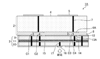
- FIG. 4 is a side perspective view showing the antenna device 1A according to the second embodiment, and the same components as those in FIG. 1 are designated by the same reference numerals and detailed description thereof will be omitted.
- the antenna device 1A is, for example, a four-element array antenna, and includes an antenna substrate 2 that radiates a signal radio wave into space through a patch element 5, and a feeding substrate 3 that feeds a signal to the antenna substrate 2.
- the feeding conductor 6A is a first feeding conductor provided at a position facing the patch element 5 via the dielectric substrate 4 of the antenna substrate 2.
- the patch element 5 and the feeding conductor 6A are electrically connected by a through hole 7.
- the feeding conductor 13A is a second feeding conductor provided on the main surface of the feeding board 3 on the antenna board 2 side.
- the circular feeding conductor 13A is provided so as not to be electrically connected to the main plate 12, and is electrically connected to the 4-distribution synthesis circuit 15 by the vertical feeding portion 14.
- the feeding conductor 6A has a larger area than the feeding conductor 13A.
- FIG. 5 is a side perspective view showing the antenna device 1A in which the position shift occurs between the antenna substrate 2 and the feeding substrate 3.
- the antenna substrate 2 and the feeding substrate 3 are misaligned to the extent that the feeding conductor 13A moves within the diameter range of the circular feeding conductor 6A.
- the amount of change in the capacitance component generated between the feeding conductor 6A and the feeding conductor 13A shown by B1 and B2 is small. Therefore, the deterioration of the reflection characteristic due to the change in the facing area between the feeding conductor 6A and the feeding conductor 13A is reduced.
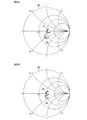
- FIG. 6A is a Smith chart diagram showing the input impedance of a single patch element 5 in the antenna device 1 before and after a positional shift occurs between the antenna substrate 2 and the feeding substrate 3.
- FIG. 6B is a Smith chart diagram showing the input impedance of a single patch element 5 in the antenna device 1A before and after a positional shift occurs between the antenna substrate 2 and the feeding substrate 3.
- the charts shown in FIGS. 6A and 6B show that the closer to the center of the circle in the chart, the smaller the reflection, and the closer to the edge of the circle, the greater the reflection.
- the solid line 31 and the solid line 33 show the reflection characteristics when there is no positional deviation between the antenna substrate 2 and the feeding substrate 3.
- the broken line 32 and the broken line 34 show the reflection characteristics when a positional deviation of 0.015 ⁇ c is applied between the antenna substrate 2 and the feeding substrate 3.
- ⁇ c is the design center frequency of the antenna devices 1 and 1A.
- the double-headed arrows shown in FIGS. 6A and 6B indicate the amount of change in input impedance at the same frequency.
- the feeding conductor 13A moves within the diameter of the feeding conductor 6A.
- the feeding conductor 6 and the feeding conductor 13 have the same area, if a misalignment of 0.015 ⁇ c occurs between the antenna substrate 2 and the feeding substrate 3, the feeding conductor 6 and the feeding conductor 6 The area facing the power feeding conductor 13 changes (decreases).
- the length of the arrow shown in FIG. 6B is shorter than the length of the arrow shown in FIG. 6A due to the change in the facing area between the feeding conductor 6 and the feeding conductor 13. That is, the amount of change in the input impedance in the antenna device 1A shown in FIG. 6B is smaller than the amount of change in the input impedance in the antenna device 1 shown in FIG. 6A.
- the feeding conductor 6A is formed to have a larger area than the feeding conductor 13A.
- the antenna device 1A can reduce the influence on the input impedance, that is, the deterioration of the reflection characteristics, caused by the positional deviation between the antenna substrate 2 and the feeding substrate 3.
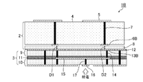
- FIG. 7 is a side perspective view showing the antenna device 1B according to the third embodiment, and the same components as those in FIG. 1 are designated by the same reference numerals, and detailed description thereof will be omitted.
- the antenna device 1B is, for example, a four-element array antenna, and includes an antenna substrate 2 that radiates a signal radio wave into space through a patch element 5, and a feeding substrate 3 that feeds a signal to the antenna substrate 2.
- the feeding conductor 6B is a first feeding conductor provided at a position facing the patch element 5 via the dielectric substrate 4 of the antenna substrate 2.
- the patch element 5 and the feeding conductor 6B are electrically connected by a through hole 7.
- the feeding conductor 13B is a second feeding conductor provided on the main surface of the feeding board 3 on the antenna board 2 side.
- the circular feeding conductor 13B is provided so as not to be electrically connected to the main plate 12, and is electrically connected to the 4-distribution synthesis circuit 15 by the vertical feeding portion 14.
- the feeding conductor 6B has a smaller area than the feeding conductor 13B.
- the antenna device 1B can be referred to as the feeding conductor 6B as long as the feeding conductor 6B moves within the diameter of the feeding conductor 13B even if the position of the antenna device 1B is displaced between the antenna substrate 2 and the feeding conductor 3. There is no change in the facing area of the feeding conductor 13B, and the deterioration of the reflection characteristics due to the change in the facing area of the feeding conductor 6B and the feeding conductor 13B is reduced.
- FIG. 8 is a side perspective view showing the antenna device 1A in which the position shift occurs between the antenna substrate 2 and the feeding substrate 3.
- the feeding conductor 6A is larger than the area of the feeding conductor 13A, when the positional deviation between the antenna substrate 2 and the feeding substrate 3 is large, as shown by arrows C2 and C4 in FIG. 8, the feeding conductor A portion where the feeding conductor 6A and the feeding conductor 13A face each other and a portion where the feeding conductor 6A and the main plate 12 of the feeding substrate 3 face each other are generated as shown by arrows C1 and C3.
- FIG. 9 is a side perspective view showing the antenna device 1B in which the position shift occurs between the antenna substrate 2 and the feeding substrate 3.
- the feeding conductor 13B is larger than the area of the feeding conductor 6B, and there is no main plate around the feeding conductor 6B on the main surface of the dielectric substrate 4.
- the antenna device 1A is displaced so that the feeding conductor 6A faces the main plate 12, the feeding conductor 6B does not face a portion other than the feeding conductor 13B.
- FIG. 10A is a Smith chart diagram showing the input impedance of a single patch element 5 in the antenna device 1A before and after a positional shift occurs between the antenna substrate 2 and the feeding substrate 3.
- FIG. 10B is a Smith chart diagram showing the input impedance of a single patch element 5 in the antenna device 1B before and after a positional shift occurs between the antenna substrate 2 and the feeding substrate 3.
- the charts shown in FIGS. 10A and 10B show that the closer to the center of the circle in the chart, the smaller the reflection, and the closer to the edge of the circle, the larger the reflection.
- the solid line 33 and the solid line 36 show the reflection characteristics when there is no positional deviation between the antenna substrate 2 and the feeding substrate 3.
- the broken line 35 and the broken line 37 show the reflection characteristics when a positional deviation of 0.02 ⁇ c is applied between the antenna substrate 2 and the feeding substrate 3.
- ⁇ c is the design center frequency of the antenna devices 1A and 1B.
- the double-headed arrows shown in FIGS. 10A and 10B indicate the amount of change in input impedance at the same frequency.
- the feeding conductor 6B moves within the diameter of the feeding conductor 13B.
- the feeding conductor 6A when a positional deviation of 0.02 ⁇ c occurs between the antenna substrate 2 and the feeding substrate 3 and the feeding conductor 6A faces the main plate 12 adjacent to the feeding conductor 13A, the feeding conductor 6A The area facing the feeding conductor 13A changes (decreases).
- the length of the arrow shown in FIG. 10B is shorter than the length of the arrow shown in FIG. 10A. That is, the amount of change in the input impedance in the antenna device 1B shown in FIG. 10B is smaller than the amount of change in the input impedance in the antenna device 1A shown in FIG. 10A.
- the feeding conductor 13B is formed to have a larger area than the feeding conductor 6B.
- the antenna device 1B can reduce the influence on the input impedance, that is, the deterioration of the reflection characteristics, caused by the positional deviation between the antenna substrate 2 and the feeding substrate 3.
- FIG. 11 is a side perspective view showing the antenna device 1C according to the fourth embodiment, and the same components as those in FIG. 1 are designated by the same reference numerals, and detailed description thereof will be omitted.
- FIG. 12 is a top view showing the antenna device 1C.
- the antenna device 1C is, for example, a four-element array antenna, and includes an antenna substrate 2 that radiates a signal radio wave into space through a patch element 5, and a feeding substrate 3 that feeds a signal to the antenna substrate 2.
- the antenna board 2, the power feeding board 3, and the dielectric 8 are provided with through holes 41 through which the screws 40 pass when they are stacked.
- the antenna board 2 and the power feeding board 3 in a state where the dielectric 8 is sandwiched are fixed. Since it is necessary to pass the screw 40 through the through hole 41 in the antenna device 1C, the opening diameter R2 of the through hole 41 is formed to be larger than the diameter R1 of the screw 40, as shown in FIG.
- the dimension of the feeding conductor 13C is formed to be larger than the dimension of the feeding conductor 6C by the difference between the diameter R1 of the screw 40 and the opening diameter R2 of the through hole 41.
- the facing area of the feeding conductor 6C and the feeding conductor 13C changes. It can be suppressed and the deterioration of the reflection characteristics accompanying this can be reduced.
- the antenna device 1C even if the dimension of the feeding conductor 6C is formed to be larger than the dimension of the feeding conductor 13C by the difference between the diameter R1 of the screw 40 and the opening diameter R2 of the through hole 41, the same effect can be obtained. can get.
- FIG. 13 is a side perspective view showing the antenna device 1D which is a modified example of the antenna device 1C, and the same components as those in FIG. 1 are designated by the same reference numerals and detailed description thereof will be omitted.
- FIG. 14 is a top view showing the antenna device 1D.
- the antenna device 1D is, for example, a four-element array antenna, and includes an antenna substrate 2 that radiates a signal radio wave into space through a patch element 5, and a feeding substrate 3 that feeds a signal to the antenna substrate 2.
- the frame member 42 integrally supports the antenna substrate 2, the feeding substrate 3, and the dielectric 8 in the state where the dielectric 8 is sandwiched between the antenna substrate 2 and the feeding substrate 3. It is fixed.
- the antenna substrate 2, the feeding substrate 3, and the dielectric 8 need to be housed in the frame member 42. Therefore, as shown in FIG. 14, the inner dimension R3 of the frame member 42 is the antenna substrate 2, The power feeding board 3 and the dielectric 8 are formed to be larger than the external dimensions L1.
- the dimension of the feeding conductor 13D is formed to be larger than the dimension of the feeding conductor 6D by the difference between the outer dimension L1 and the inner dimension R3.
- the antenna substrate 2 and the feeding substrate 3 are displaced by the difference between the external dimension L1 and the inner dimension R3, the change in the facing area between the feeding conductor 6D and the feeding conductor 13D is suppressed. It is possible to reduce the deterioration of the reflection characteristics due to the above.
- the antenna device 1D the same effect can be obtained even if the dimension of the feeding conductor 6D is formed to be larger than the dimension of the feeding conductor 13D by the difference between the external dimension L1 and the inner dimension R3.
- FIG. 15 is a plan view showing an example of the feeding conductor 6C of the antenna substrate 2 in the antenna device 1C.
- FIG. 16 is a plan view showing an example of the power feeding conductor 13C of the power feeding substrate 3 in the antenna device 1C.
- the misalignment between the antenna substrate 2 and the feeding substrate 3 is caused by the difference between the diameter R1 of the screw 40 and the opening diameter R2 of the through hole 41 as a play. Therefore, since the screw 40 moves in the through hole 41, the individual screw fastening portions are displaced in a circular range when viewed from above.
- the feeding conductor having a larger dimension has a circular shape as shown in FIGS. 15 and 16.
- the feeding conductor having the larger dimension can be formed with the minimum size including the range in which the misalignment can occur, so that the layout of the feeding structure can be saved.
- FIG. 17 is a plan view showing an example of the feeding conductor 6D of the antenna substrate 2 in the antenna device 1D.
- FIG. 18 is a plan view showing an example of the power feeding conductor 13D of the power feeding substrate 3 in the antenna device 1D.
- the positional deviation between the antenna substrate 2 and the feeding substrate 3 is caused by the difference between the external dimension L1 and the inner dimension R3 as a play. Therefore, the multilayer board in which the antenna board 2 and the power feeding board 3 are multilayered with the dielectric 8 sandwiched therein moves inside the frame member 42, and the position shift occurs in a rectangular range when viewed from the upper surface.
- the feeding conductor having a larger dimension has a rectangular shape as shown in FIGS. 17 and 18.
- the feeding conductor having the larger dimension can be formed with the minimum size including the range in which the misalignment can occur, so that the layout of the feeding structure can be saved.
- the antenna device 1C includes a through hole 41 penetrating the antenna board 2, the feeding board 3 and the dielectric 8, and the antenna board 2 and the feeding board 3 passing through the through hole 41.
- a screw 40 for fixing the dielectric 8 in a sandwiched state is provided.
- the antenna device 1C can fix the antenna substrate 2, the feeding substrate 3, and the dielectric 8 by the screws 40 and the through holes 41.
- the antenna device 1D supports the antenna substrate 2, the feeding substrate 3 and the dielectric 8 inside, and integrally fixes the dielectric 8 in a state of sandwiching the dielectric 8 between the antenna substrate 2 and the feeding substrate 3.
- a frame member 42 is provided. In the antenna device 1D, the antenna substrate 2, the feeding substrate 3, and the dielectric 8 can be fixed by the frame member 42.
- FIG. 19 is a side perspective view showing the antenna device 1E according to the fifth embodiment, and the same components as those in FIG. 1 are designated by the same reference numerals, and detailed description thereof will be omitted.
- FIG. 20 is an exploded perspective view showing a substrate of each layer in the antenna device 1E.
- the antenna device 1E is, for example, a four-element array antenna, and includes an antenna substrate 2 that radiates a signal radio wave into space through a patch element 5, and a feeding substrate 3A that feeds a signal to the antenna substrate 2.
- the power supply substrate 3A is a multilayer substrate in which a substrate 9 and a substrate 10 having substantially the same thickness are bonded in a plurality of stages (two stages in FIG. 19) by an adhesive layer 11.
- a main plate 12 and a feeding conductor 13 are provided on the main surface of the feeding board 3A on the antenna board 2 side.
- the power feeding unit 16a and the power feeding unit 16b are provided on the main surface of the power feeding board 3A on the opposite side of the antenna board 2.
- the 4-distribution synthesis circuit 15 and the feeding unit 16b are electrically connected by a vertical feeding unit 17.
- a 4-distribution synthesis circuit 15a is provided among the substrates constituting the feeding substrate 3A.
- the 4-distribution synthesis circuit 15a is composed of a triplate line, distributes a signal to be transmitted to the patch element 5, and synthesizes a signal from the patch element 5.
- FIG. 21 is a top view showing the patch element 5 of the antenna device 1E.
- FIG. 22 is a top view showing a modified example of the patch element 5 of the antenna device 1E.
- the patch element 5 may be probe-fed at two feeding points as shown in FIGS. 19, 20 and 21, or may be probe-fed at four feeding points as shown in FIG. ..
- the patch element 5 fed at two or more feeding points can make a signal radiated as a radio wave circularly polarized, bipolarized, or lowly cross-polarized.
- the multi-layered power supply substrate 3A can be provided with a filter that blocks signals of unnecessary frequency components by, for example, being configured by a triplate line, and a phase difference can be added to the signals fed to each patch element 5.
- a power supply circuit such as a hybrid circuit can be provided.
- the antenna device 1E in which the feeding board 3A having such a circuit is combined with the antenna board 2 can realize an antenna having a thin flat surface and high functionality.
- FIG. 23 is a side perspective view showing the antenna device 1F which is a modified example of the antenna device 1E, and the same components as those in FIG. 1 are designated by the same reference numerals and detailed description thereof will be omitted.
- the antenna device 1F is, for example, a 4-element array antenna, and includes an antenna substrate 2A and a feeding substrate 3.
- the antenna substrate 2A is configured by stacking a dielectric substrate 4A, which is a non-exciting element substrate, on a dielectric substrate 4 in order to widen the frequency band used by the antenna device 1F. ..
- a non-excited patch element 5A is provided on the main surface of the dielectric substrate 4A on the opposite side of the dielectric substrate 4 from the dielectric substrate 4.
- the signal fed from the feeding board 3 to the antenna board 2A is radiated into space through the patch element 5.
- the antenna substrate 2A is configured by stacking a plurality of substrates, but is not a multilayer substrate including the power feeding substrate 3. Therefore, the stress generated when the antenna substrate 2A and the feeding substrate 3 are attached to each other is absorbed by the misalignment of both substrates. Therefore, the antenna device 1F realizes a thin antenna because warpage does not occur even if a substrate having the same thickness as the antenna substrate 2A is not multi-layered on the main surface of the feeding substrate 3 opposite to the antenna substrate 2A. be able to.
- the power feeding substrate 3A is a multilayer substrate composed of a plurality of dielectric substrates. Since various circuits can be provided on the power feeding board 3A, the antenna device 1E can realize an antenna having a thin flat surface and high functionality.
- the antenna substrate 2A is a multilayer substrate composed of a plurality of dielectric substrates. Since the antenna substrate 2A becomes thicker, the frequency band used by the antenna device 1F is widened.
- FIG. 24 is a top view showing Example 1 of the patch element.
- FIG. 25 is a top view showing Example 2 of the patch element.
- FIG. 26 is a top view showing Example 3 of the patch element.
- FIG. 27 is a top view showing Example 4 of the patch element.
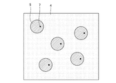
- the antenna device shown in the first to fifth embodiments may be an antenna in which a single patch element 5 is provided on the dielectric substrate 4, or is shown in FIG. 25. As shown, it may be a linear array antenna in which a plurality of patch elements 5 are linearly arranged on a dielectric substrate 4. Further, the antenna device shown in the first to fifth embodiments may be an antenna in which a plurality of patch elements 5 are triangularly arranged on the dielectric substrate 4, as shown in FIG. 26.
- the antenna may be an antenna in which a plurality of patch elements 5 are aperiodically arranged on the dielectric substrate 4.
- the antenna devices shown in the first to fifth embodiments can realize various arrangements of the patch elements 5, and the degree of freedom in antenna design is high.
- the antenna device according to the present disclosure can be used as a radar device, for example.
- 1,1A, 1B, 1C, 1D, 1E, 1F antenna device 2,2A antenna board, 3,3A power supply board, 4,4A dielectric board, 5 patch element, 5A non-excitation patch element, 6,6A, 6B , 6C, 6D feed conductor, 7 through hole, 8 dielectric, 9, 10 substrate, 11 adhesive layer, 12 main plate, 13, 13A, 13B, 13C, 13D feed conductor, 14, 17 vertical feed section, 15, 15a 4 Distribution synthesis circuit, 16, 16a, 16b power feeding part, 40 screws, 41 through holes, 42 frame members, 100 loads, 101 inductance components, 102 capacitance components.
Landscapes
- Waveguide Aerials (AREA)
- Variable-Direction Aerials And Aerial Arrays (AREA)
Abstract
アンテナ装置(1)は、アンテナ基板(2)と、アンテナ基板(2)に設けられたパッチ素子(5)と、アンテナ基板(2)に設けられた給電導体(6)と、アンテナ基板(2)側に伝送される信号を給電する給電部(16)を有した給電基板(3)と、アンテナ基板(2)を貫通してパッチ素子(5)と給電導体(6)とを電気的に接続するスルーホール(7)と、給電基板(3)に設けられた給電導体(13)と、アンテナ基板(2)と給電基板(3)との間に設けられた中間基板(8)とを備え、給電導体(6)と給電導体(13)とが、中間基板(8)を挟んで容量性結合している。
Description
本開示は、アンテナ装置に関する。
アンテナ基板上に設けられた放射導体(パッチ素子)への信号の給電方法の一つとしてプローブ給電がある。プローブ給電は、スロットを用いた電磁結合による給電する方法に比べて、給電構造が省スペースである。このため、信号の直交二偏波化、円偏波化または低交差偏波化の用途において、単一のパッチ素子の多点給電に適している。
プローブ給電を行うアンテナ装置において、使用周波数帯域を広帯域化するためには、アンテナ基板を厚くすることが知られている。アンテナ基板が厚くなると、その分だけ、プローブが長くなるため、そのインダクタンス成分が大きくなり、パッチ素子と給電回路との間のインダクタンス整合がとれなくなる可能性がある。
例えば、非特許文献1には、プローブの先端部分に導体ランドを形成し、パッチ素子と導体ランドとの間に生じるキャパシタンス成分によってプローブのインダクタンス成分を補償する技術が記載されている。
FONG, K. S., PUES, H. F., and WITHERS, M. J., " Wideband multilayer coaxial-fed microstrip antenna element ", Electron Lett., 1985, 21, pp.497-499.
非特許文献1に記載された従来の技術は、アンテナ基板に設けられたパッチ素子と給電基板とを電気的に接続するスルーホールを形成する必要があるため、給電基板にアンテナ基板を積み重ねる多層化が必要である。しかしながら、複数の基板を積み重ねた多層基板において各基板の厚さが層厚方向に概ね対称になっていないと、多層基板に反りが生じる虞がある。このため、従来のアンテナ装置において、使用周波数帯域を広帯域化するためにアンテナ基板が給電基板よりも厚くされた場合、給電基板におけるアンテナ基板側とは反対側の面に、アンテナ基板と同様な厚さの基板をさらに設ける必要があり、基板全体の厚さが増大するという課題があった。
本開示は上記課題を解決するものであり、基板全体の厚さの増大を軽減することができるアンテナ装置を得ることを目的とする。
本開示に係るアンテナ装置は、平板状のアンテナ基板と、アンテナ基板に設けられた1または複数の放射導体と、アンテナ基板における放射導体とは反対側の主面に設けられた第1の給電導体と、アンテナ基板側に伝送される信号を給電する給電部が設けられた平板状の給電基板と、アンテナ基板を貫通して放射導体と第1の給電導体とを電気的に接続するスルーホールと、給電基板におけるアンテナ基板側の主面に設けられた第2の給電導体と、アンテナ基板と給電基板との間に設けられた中間基板とを備え、第1の給電導体と第2の給電導体とが、中間基板を挟んで容量性結合している。
本開示によれば、アンテナ基板に設けられた第1の給電導体と、給電基板に設けられた第2の給電導体とが中間基板を挟んで容量性結合しているので、アンテナ基板と給電基板との間に設けられたスルーホールが途中で分断されていても、給電基板からアンテナ基板にプローブ給電することができる。中間基板を基準として、アンテナ基板と給電基板との厚さが層厚方向で概ね対称となるように多層化することができるので、給電基板におけるアンテナ基板を設けた側とは反対側の面にアンテナ基板と同様な厚さの基板を設ける必要がない。これにより、本開示に係るアンテナ装置では、基板全体の厚さの増大を軽減することができる。
実施の形態1.
図1は、実施の形態1に係るアンテナ装置1を示す側面透視図である。図2は、図1のアンテナ装置1における各層の基板を示す分解斜視図である。図1および図2において、アンテナ装置1は、4つのパッチ素子5を有した4素子アレーアンテナであり、パッチ素子5を通じて信号の電波を空間に放射するアンテナ基板2と、アンテナ基板2に信号を給電する給電基板3とを備える。パッチ素子5は、例えば、円形状の放射導体であり、電波を放射する放射素子として機能する。
図1は、実施の形態1に係るアンテナ装置1を示す側面透視図である。図2は、図1のアンテナ装置1における各層の基板を示す分解斜視図である。図1および図2において、アンテナ装置1は、4つのパッチ素子5を有した4素子アレーアンテナであり、パッチ素子5を通じて信号の電波を空間に放射するアンテナ基板2と、アンテナ基板2に信号を給電する給電基板3とを備える。パッチ素子5は、例えば、円形状の放射導体であり、電波を放射する放射素子として機能する。
アンテナ基板2は、平板状の誘電体基板4によって構成されており、この誘電体基板4の主面にはパッチ素子5が設けられ、誘電体基板4のパッチ素子5とは反対側の主面には給電導体6が設けられている。円形状の給電導体6は、誘電体基板4を介してパッチ素子5と対向した位置に設けられた第1の給電導体である。パッチ素子5と給電導体6の間は、スルーホール7によって電気的に接続されている。スルーホール7は、パッチ素子5に信号を給電するプローブである。また、アンテナ基板2は、給電基板3側の主面上に、中間基板である平板状の誘電体8を備えている。
給電基板3は、概ね同じ厚さの基板9と基板10が接着層11によって貼り合わされた多層基板である。給電基板3におけるアンテナ基板2側の主面には、地板12と給電導体13とが設けられている。円形状の給電導体13は、垂直給電部14によって4分配合成回路15に電気的に接続された第2の給電導体であり、地板12と導通しないように設けられている。例えば、4分配合成回路15は、トリプレート線路で構成されている。給電部16は、給電基板3におけるアンテナ基板2とは反対側の主面に設けられる。4分配合成回路15と給電部16は、垂直給電部17によって電気的に接続されている。給電導体6と給電導体13は、誘電体8によって物理的に接触していない。
アンテナ装置1において、給電部16に入力された信号は、垂直給電部17、4分配合成回路15および垂直給電部14を伝搬することにより、給電導体13に給電される。給電導体6と給電導体13とは、誘電体8を挟んで容量性結合している。これにより、給電導体13に伝搬した信号は、給電導体6に伝搬され、スルーホール7を通じてパッチ素子5に給電される。
スルーホール7は、長くかつその径が小さいほど、インダクタンス成分が大きくなる。また、給電導体6と給電導体13との間に存在するキャパシタンス成分は、給電導体6と給電導体13とが対向する面積に比例するが、給電導体6と給電導体13との間の距離に反比例する。なお、実施の形態1において、給電導体6および給電導体13は、例えば、同じ面積である。
図3は、給電部16からアンテナ基板2側をみた等価回路を示す回路図である。図3において、アンテナ装置1の入力インピーダンスAは、パッチ素子5の並列共振回路の負荷100に対して、スルーホール7のインダクタンス成分101と、給電導体6と給電導体13との間のキャパシタンス成分102とが直列で接続されている。
図3に示す等価回路において、負荷100に含まれるインダクタンス成分とキャパシタンス成分は相殺されるので、抵抗成分のみが残る。また、負荷100に直列に接続されたインダクタンス成分101は、直列に接続されたキャパシタンス成分102によって打ち消される。これにより、アンテナ基板2の使用周波数帯域を広帯域化するために、誘電体基板4が厚くされ、これに伴ってスルーホール7が長くなっても、アンテナ装置1では、インダクタンス整合をとることが可能である。
また、アンテナ装置1では、給電導体6と給電導体13とが容量性結合しているので、垂直給電部14とスルーホール7が分断されていても、給電基板3からの信号がアンテナ基板2へ給電される。このため、アンテナ装置1は、アンテナ基板2と給電基板3を個別に製造し、給電基板3上にアンテナ基板2を積み重ねるだけで製造可能である。従って、アンテナ基板2および給電基板3の両者を多層化する必要がない。
以上のように、実施の形態1に係るアンテナ装置1において、アンテナ基板2に設けられた給電導体6と給電基板3に設けられた給電導体13とが誘電体8を挟んで容量性結合しているので、アンテナ基板2と給電基板3との間に設けられたスルーホール7と垂直給電部14とが途中で分断されていても、給電基板3からアンテナ基板2にプローブ給電することができる。誘電体8を基準として、アンテナ基板2と給電基板3の厚さが層厚方向で概ね対称となるように多層化することができるので、給電基板3におけるアンテナ基板2側とは反対側の面にアンテナ基板2と同様な厚さの基板を設ける必要がない。これにより、アンテナ装置1は、基板全体の厚さの増大を軽減することができる。
実施の形態2.
実施の形態2に係るアンテナ装置は、実施の形態1と同様の効果が得られるとともに、多層化したアンテナ基板と給電基板との位置ずれによる特性劣化の影響を緩和することができる。例えば、給電基板上にアンテナ基板を固定するために、積み重ねた基板の四隅をねじ止めすることがある。この固定構造は、ねじの径よりも貫通穴の開口径を大きくする必要があるため、ねじの径と貫通穴の開口径との差が遊びとなって積み重ねた基板の位置ずれが生じる可能性がある。例えば、アンテナ装置1において、アンテナ基板2と給電基板3の間で位置ずれが生じると、給電導体6と給電導体13の対向面積が変化するため、反射特性が劣化する。
実施の形態2に係るアンテナ装置は、実施の形態1と同様の効果が得られるとともに、多層化したアンテナ基板と給電基板との位置ずれによる特性劣化の影響を緩和することができる。例えば、給電基板上にアンテナ基板を固定するために、積み重ねた基板の四隅をねじ止めすることがある。この固定構造は、ねじの径よりも貫通穴の開口径を大きくする必要があるため、ねじの径と貫通穴の開口径との差が遊びとなって積み重ねた基板の位置ずれが生じる可能性がある。例えば、アンテナ装置1において、アンテナ基板2と給電基板3の間で位置ずれが生じると、給電導体6と給電導体13の対向面積が変化するため、反射特性が劣化する。
図4は、実施の形態2に係るアンテナ装置1Aを示す側面透視図であり、図1と同一の構成要素には同一の符号を付して詳細な説明は省略する。アンテナ装置1Aは、例えば、4素子アレーアンテナであり、パッチ素子5を通じて信号の電波を空間に放射するアンテナ基板2と、信号をアンテナ基板2に給電する給電基板3とを備える。給電導体6Aは、アンテナ基板2の誘電体基板4を介してパッチ素子5と対向した位置に設けられた第1の給電導体である。パッチ素子5と給電導体6Aは、スルーホール7によって電気的に接続されている。
給電導体13Aは、給電基板3におけるアンテナ基板2側の主面上に設けられた第2の給電導体である。円形状の給電導体13Aは、地板12とは導通しないように設けられており、垂直給電部14によって4分配合成回路15に電気的に接続されている。実施の形態2において、給電導体6Aは給電導体13Aよりも面積が大きい。
図5は、アンテナ基板2と給電基板3との間に位置ずれが生じたアンテナ装置1Aを示す側面透視図である。図5において、円形状の給電導体6Aの径の範囲内で給電導体13Aが移動する程度にアンテナ基板2と給電基板3が位置ずれしている。この場合、給電導体6Aと給電導体13Aとの対向面積には変化がなく、B1およびB2で示す給電導体6Aと給電導体13Aの間に生じるキャパシタンス成分の変化量は小さい。従って、給電導体6Aと給電導体13Aとの対向面積の変化に起因した反射特性の劣化が低減される。
図6Aは、アンテナ基板2と給電基板3との間に位置ずれが生じる前後のアンテナ装置1における単体のパッチ素子5の入力インピーダンスを示すスミスチャート図である。図6Bは、アンテナ基板2と給電基板3との間に位置ずれが生じる前後のアンテナ装置1Aにおける単体のパッチ素子5の入力インピーダンスを示すスミスチャート図である。図6Aおよび図6Bに示すチャートは、チャート中の円の中心に近いほど反射が小さく、円の端に近いほど反射が大きいことを示している。
実線31および実線33は、アンテナ基板2と給電基板3との間に位置ずれがない場合における反射特性を示している。破線32および破線34は、アンテナ基板2と給電基板3との間に0.015λcの位置ずれを与えた場合における反射特性を示している。λcはアンテナ装置1および1Aの設計中心周波数である。図6Aおよび図6Bに示す両矢印は、同一周波数での入力インピーダンスの変化量を示している。
例えば、アンテナ装置1Aは、アンテナ基板2と給電基板3との間に0.015λcの位置ずれが生じても給電導体6Aの径の範囲内で給電導体13Aが移動する程度である。これに対して、アンテナ装置1は、給電導体6と給電導体13とが同じ面積であるため、アンテナ基板2と給電基板3との間に0.015λcの位置ずれが生じると、給電導体6と給電導体13との対向面積は変化(減少)する。
給電導体6と給電導体13との対向面積の変化によって、図6Aに示す矢印の長さよりも図6Bに示す矢印の長さが短くなっている。すなわち、図6Aに示すアンテナ装置1における入力インピーダンスの変化量よりも、図6Bに示すアンテナ装置1Aにおける入力インピーダンスの変化量が小さくなっている。
以上のように、実施の形態2に係るアンテナ装置1Aにおいて、給電導体6Aは、給電導体13Aよりも面積が大きく形成されている。これにより、アンテナ装置1Aは、アンテナ基板2と給電基板3との位置ずれに起因した入力インピーダンスへの影響、すなわち反射特性の劣化を低減することができる。
実施の形態3.
図7は、実施の形態3に係るアンテナ装置1Bを示す側面透視図であり、図1と同一の構成要素には同一の符号を付して詳細な説明は省略する。アンテナ装置1Bは、例えば、4素子アレーアンテナであり、パッチ素子5を通じて信号の電波を空間に放射するアンテナ基板2と、信号をアンテナ基板2に給電する給電基板3とを備える。給電導体6Bは、アンテナ基板2の誘電体基板4を介してパッチ素子5と対向した位置に設けられた第1の給電導体である。パッチ素子5と給電導体6Bは、スルーホール7によって電気的に接続されている。
図7は、実施の形態3に係るアンテナ装置1Bを示す側面透視図であり、図1と同一の構成要素には同一の符号を付して詳細な説明は省略する。アンテナ装置1Bは、例えば、4素子アレーアンテナであり、パッチ素子5を通じて信号の電波を空間に放射するアンテナ基板2と、信号をアンテナ基板2に給電する給電基板3とを備える。給電導体6Bは、アンテナ基板2の誘電体基板4を介してパッチ素子5と対向した位置に設けられた第1の給電導体である。パッチ素子5と給電導体6Bは、スルーホール7によって電気的に接続されている。
給電導体13Bは、給電基板3におけるアンテナ基板2側の主面上に設けられた第2の給電導体である。円形状の給電導体13Bは、地板12とは導通しないように設けられており、垂直給電部14によって4分配合成回路15に電気的に接続されている。実施の形態3において、給電導体6Bは、給電導体13Bよりも面積が小さい。これにより、アンテナ装置1Bは、アンテナ基板2と給電基板3との間に位置ずれが生じても、給電導体13Bの径の範囲内で給電導体6Bが移動する程度であれば、給電導体6Bと給電導体13Bとの対向面積には変化がなく、給電導体6Bと給電導体13Bの対向面積の変化に起因した反射特性の劣化が低減される。
図8は、アンテナ基板2と給電基板3との間に位置ずれが生じたアンテナ装置1Aを示す側面透視図である。アンテナ装置1Aは、給電導体6Aが給電導体13Aの面積よりも大きいので、アンテナ基板2と給電基板3との間の位置ずれが大きい場合、図8において矢印C2およびC4に示すように、給電導体6Aと給電導体13Aが対向する部分と、矢印C1およびC3に示すように、給電導体6Aと給電基板3の地板12とが対向する部分が生じる。
図9は、アンテナ基板2と給電基板3との間に位置ずれが生じたアンテナ装置1Bを示す側面透視図である。アンテナ装置1Bは、給電導体13Bが給電導体6Bの面積よりも大きく、誘電体基板4の主面において給電導体6Bの周囲には地板が存在しない。これにより、アンテナ装置1Aにおいて給電導体6Aが地板12に対向するほどの位置ずれが、アンテナ装置1Bに発生しても、給電導体6Bは、給電導体13B以外の部分と対向することはない。
図10Aは、アンテナ基板2と給電基板3との間に位置ずれが生じる前後のアンテナ装置1Aにおける単体のパッチ素子5の入力インピーダンスを示すスミスチャート図である。図10Bは、アンテナ基板2と給電基板3との間に位置ずれが生じる前後のアンテナ装置1Bにおける単体のパッチ素子5の入力インピーダンスを示すスミスチャート図である。図10Aおよび図10Bに示すチャートは、チャート中の円の中心に近いほど、反射が小さく、円の端に近いほど、反射が大きいことを示している。
実線33および実線36は、アンテナ基板2と給電基板3との間に位置ずれがない場合における反射特性を示している。破線35および破線37は、アンテナ基板2と給電基板3との間に0.02λcの位置ずれを与えた場合における反射特性を示している。λcはアンテナ装置1Aおよび1Bの設計中心周波数である。図10Aおよび図10Bに示す両矢印は、同一周波数での入力インピーダンスの変化量を示している。
例えば、アンテナ装置1Bは、アンテナ基板2と給電基板3との間に0.02λcの位置ずれが生じても、給電導体13Bの径の範囲内で給電導体6Bが移動する程度である。これに対して、アンテナ装置1Aは、アンテナ基板2と給電基板3との間に0.02λcの位置ずれが生じて、給電導体6Aが給電導体13Aに隣接した地板12に対向すると、給電導体6Aと給電導体13Aとの対向面積は変化(減少)する。
給電導体6Aと給電導体13Aの対向面積の変化によって、図10Aに示す矢印の長さよりも図10Bに示す矢印の長さが短くなっている。すなわち、図10Aに示すアンテナ装置1Aにおける入力インピーダンスの変化量よりも、図10Bに示すアンテナ装置1Bにおける入力インピーダンスの変化量が小さくなっている。
以上のように、実施の形態3に係るアンテナ装置1Bにおいて、給電導体13Bは、給電導体6Bよりも面積が大きく形成されている。これにより、アンテナ装置1Bは、アンテナ基板2と給電基板3との位置ずれに起因した入力インピーダンスへの影響、すなわち反射特性の劣化を低減することができる。
実施の形態4.
図11は、実施の形態4に係るアンテナ装置1Cを示す側面透視図であり、図1と同一の構成要素には同一の符号を付して詳細な説明は省略する。図12は、アンテナ装置1Cを示す上面図である。アンテナ装置1Cは、例えば、4素子アレーアンテナであり、パッチ素子5を通じて信号の電波を空間に放射するアンテナ基板2と、信号をアンテナ基板2に給電する給電基板3を備える。
図11は、実施の形態4に係るアンテナ装置1Cを示す側面透視図であり、図1と同一の構成要素には同一の符号を付して詳細な説明は省略する。図12は、アンテナ装置1Cを示す上面図である。アンテナ装置1Cは、例えば、4素子アレーアンテナであり、パッチ素子5を通じて信号の電波を空間に放射するアンテナ基板2と、信号をアンテナ基板2に給電する給電基板3を備える。
アンテナ基板2、給電基板3および誘電体8には、図11に示すように、積み重ねられたときに、ねじ40が通る貫通穴41が設けられている。貫通穴41に通されたねじ40をナットで締結することにより、誘電体8を挟んだ状態のアンテナ基板2と給電基板3とが固定される。なお、アンテナ装置1Cにおいて、ねじ40を貫通穴41に通す必要があるので、図12に示すように、貫通穴41の開口径R2はねじ40の径R1よりも大きく形成される。
ねじ40の径R1よりも貫通穴41の開口径R2が大きいと、ねじ40の径R1と貫通穴41の開口径R2との差が遊びとなってアンテナ基板2と給電基板3との間に位置ずれが生じる可能性がある。そこで、アンテナ装置1Cでは、給電導体13Cの寸法が、給電導体6Cの寸法よりもねじ40の径R1と貫通穴41の開口径R2との差の分だけ大きく形成されている。
これにより、アンテナ基板2と給電基板3が、ねじ40の径R1と貫通穴41の開口径R2との差の分だけ位置ずれしても、給電導体6Cと給電導体13Cの対向面積の変化が抑えられ、これに伴う反射特性の劣化を低減することができる。なお、アンテナ装置1Cにおいて、給電導体6Cの寸法が、給電導体13Cの寸法よりもねじ40の径R1と貫通穴41の開口径R2との差の分だけ大きく形成されても、同様の効果が得られる。
図13は、アンテナ装置1Cの変形例であるアンテナ装置1Dを示す側面透視図であり、図1と同一の構成要素には同一の符号を付して詳細な説明は省略する。図14は、アンテナ装置1Dを示す上面図である。アンテナ装置1Dは、例えば、4素子アレーアンテナであり、パッチ素子5を通じて信号の電波を空間に放射するアンテナ基板2と、信号をアンテナ基板2に給電する給電基板3を備える。
フレーム部材42が、図13に示すように、アンテナ基板2、給電基板3および誘電体8を内側に支持して、誘電体8を挟んだ状態のアンテナ基板2と給電基板3とを一体的に固定している。アンテナ装置1Dにおいて、アンテナ基板2、給電基板3および誘電体8が、フレーム部材42に収容される必要があるので、図14に示すように、フレーム部材42の内側寸法R3は、アンテナ基板2、給電基板3および誘電体8の外形寸法L1よりも大きく形成されている。
アンテナ基板2、給電基板3および誘電体8の外形寸法L1よりもフレーム部材42の内側寸法R3が大きいと、外形寸法L1と内側寸法R3との差が遊びとなってアンテナ基板2と給電基板3との間に位置ずれが生じる可能性がある。そこで、アンテナ装置1Dにおいては、給電導体13Dの寸法が、給電導体6Dの寸法よりも外形寸法L1と内側寸法R3との差の分だけ寸法が大きく形成されている。
これにより、アンテナ基板2と給電基板3が、外形寸法L1と内側寸法R3との差の分だけ位置ずれしても、給電導体6Dと給電導体13Dとの対向面積の変化が抑えられて、これに伴う反射特性の劣化を低減することができる。なお、アンテナ装置1Dにおいて、給電導体6Dの寸法が、給電導体13Dの寸法よりも外形寸法L1と内側寸法R3との差の分だけ大きく形成されても、同様の効果が得られる。
図15は、アンテナ装置1Cにおけるアンテナ基板2の給電導体6Cの例を示す平面図である。図16は、アンテナ装置1Cにおける給電基板3の給電導体13Cの例を示す平面図である。アンテナ装置1Cにおいて、アンテナ基板2と給電基板3との間の位置ずれは、ねじ40の径R1と貫通穴41の開口径R2の差が遊びとなって生じる。このため、ねじ40は、貫通穴41内で動くので、個々のねじ締結部は、上方から見て円形状の範囲で位置ずれが生じる。
アンテナ装置1Cにおいて、給電導体6Cまたは給電導体13Cのうち、寸法を大きくする方の給電導体は、図15および図16に示すように円形状である。これにより、アンテナ装置1Cは、寸法を大きくする方の給電導体を、位置ずれが生じ得る範囲を含む最小の寸法で形成できるので、給電構造のレイアウトを省スペース化することが可能である。
図17は、アンテナ装置1Dにおけるアンテナ基板2の給電導体6Dの例を示す平面図である。図18は、アンテナ装置1Dにおける給電基板3の給電導体13Dの例を示す平面図である。アンテナ装置1Dにおいて、アンテナ基板2と給電基板3との間の位置ずれは、外形寸法L1と内側寸法R3との差が遊びとなって生じる。このため、アンテナ基板2と給電基板3が誘電体8を挟んだ状態で多層化された多層基板は、フレーム部材42の内側で動き、上面から見て方形状の範囲で位置ずれが生じる。
アンテナ装置1Dにおいて、給電導体6Dおよび給電導体13Dのうち、寸法を大きくする方の給電導体は、図17および図18に示すように方形状である。これにより、アンテナ装置1Dは、寸法を大きくする方の給電導体を、位置ずれが生じ得る範囲を含む最小の寸法で形成できるので、給電構造のレイアウトを省スペース化することが可能である。
以上のように、実施の形態4に係るアンテナ装置1Cは、アンテナ基板2、給電基板3および誘電体8を貫通する貫通穴41と、貫通穴41を通ってアンテナ基板2と給電基板3とで誘電体8を挟んだ状態で固定するねじ40とを備える。アンテナ装置1Cは、ねじ40および貫通穴41によって、アンテナ基板2、給電基板3および誘電体8を固定することできる。
実施の形態4に係るアンテナ装置1Dは、アンテナ基板2、給電基板3および誘電体8を内側に支持して、アンテナ基板2と給電基板3で誘電体8を挟んだ状態で一体的に固定するフレーム部材42を備える。アンテナ装置1Dは、フレーム部材42によってアンテナ基板2、給電基板3および誘電体8を固定することできる。
実施の形態5.
図19は、実施の形態5に係るアンテナ装置1Eを示す側面透視図であり、図1と同一の構成要素には同一の符号を付して詳細な説明は省略する。図20は、アンテナ装置1Eにおける各層の基板を示す分解斜視図である。アンテナ装置1Eは、例えば、4素子アレーアンテナであって、パッチ素子5を通じて信号の電波を空間に放射するアンテナ基板2と、信号をアンテナ基板2に給電する給電基板3Aとを備える。
図19は、実施の形態5に係るアンテナ装置1Eを示す側面透視図であり、図1と同一の構成要素には同一の符号を付して詳細な説明は省略する。図20は、アンテナ装置1Eにおける各層の基板を示す分解斜視図である。アンテナ装置1Eは、例えば、4素子アレーアンテナであって、パッチ素子5を通じて信号の電波を空間に放射するアンテナ基板2と、信号をアンテナ基板2に給電する給電基板3Aとを備える。
給電基板3Aは、接着層11によって、概ね同じ厚さの基板9と基板10とが複数段(図19では2段)貼り合わされた多層基板である。給電基板3Aにおけるアンテナ基板2側の主面には、地板12と給電導体13とが設けられている。給電部16aおよび給電部16bは、給電基板3Aにおけるアンテナ基板2とは反対側の主面に設けられる。4分配合成回路15と給電部16bは、垂直給電部17によって電気的に接続されている。
図19および図20に示すように、給電基板3Aを構成する基板のうち、アンテナ基板2側の基板9における地板12および給電導体13が設けられた主面とは反対側の主面には、4分配合成回路15aが設けられている。4分配合成回路15aは、トリプレート線路によって構成され、パッチ素子5へ伝送する信号を分配し、パッチ素子5からの信号を合成する。
図21は、アンテナ装置1Eのパッチ素子5を示す上面図である。また、図22は、アンテナ装置1Eのパッチ素子5の変形例を示す上面図である。パッチ素子5は、図19、図20および図21に示すように、2つの給電点でプローブ給電されてもよいし、図22に示すように、4つの給電点でプローブ給電されていてもよい。2点以上の給電点で給電されるパッチ素子5は、電波として放射する信号を円偏波化、二偏波化または低交差偏波化することができる。
多層化された給電基板3Aには、例えば、トリプレート線路によって構成することで、不要な周波数成分の信号を遮断するフィルタを設けることができ、また各パッチ素子5に給電する信号に位相差を与えるハイブリッド回路などの給電回路を設けることができる。このような回路を有した給電基板3Aをアンテナ基板2と組み合わせたアンテナ装置1Eは、薄型平面でかつ高機能のアンテナを実現することができる。
図23は、アンテナ装置1Eの変形例であるアンテナ装置1Fを示す側面透視図であり、図1と同一の構成要素には同一の符号を付して詳細な説明は省略する。アンテナ装置1Fは、例えば、4素子アレーアンテナであり、アンテナ基板2Aと給電基板3を備える。アンテナ基板2Aは、図23に示すように、アンテナ装置1Fの使用周波数帯域を広帯域化するために、誘電体基板4に対して非励振素子基板である誘電体基板4Aを積み重ねて構成されている。
誘電体基板4Aにおける誘電体基板4とは反対側の主面には、非励振パッチ素子5Aが設けられている。給電基板3からアンテナ基板2Aに給電された信号は、パッチ素子5を通じて空間に放射される。アンテナ装置1Fにおいて、アンテナ基板2Aは、複数の基板を積み重ねて構成されているが、給電基板3を含んだ多層基板ではない。このため、アンテナ基板2Aと給電基板3を貼り合わせたときに生じる応力は、両基板の位置ずれによって吸収される。従って、アンテナ装置1Fは、給電基板3におけるアンテナ基板2Aとは反対側の主面にアンテナ基板2Aと同様の厚さの基板が多層化しなくても反りが生じないので、薄型のアンテナを実現することができる。
以上のように、実施の形態5に係るアンテナ装置1Eにおいて、給電基板3Aが、複数の誘電体基板により構成された多層基板である。給電基板3Aに様々な回路を設けることができるので、アンテナ装置1Eは、薄型平面でかつ高機能のアンテナを実現することができる。
実施の形態5に係るアンテナ装置1Fにおいて、アンテナ基板2Aが、複数の誘電体基板により構成された多層基板である。アンテナ基板2Aが厚くなるので、アンテナ装置1Fの使用周波数帯域が広帯域化される。
図24は、パッチ素子の例1を示す上面図である。図25は、パッチ素子の例2を示す上面図である。図26は、パッチ素子の例3を示す上面図である。図27は、パッチ素子の例4を示す上面図である。実施の形態1から実施の形態5に示したアンテナ装置は、図24に示すように、誘電体基板4上に単一のパッチ素子5が設けられたアンテナであってもよいし、図25に示すように、誘電体基板4上に複数のパッチ素子5が直線状に並んだリニアアレーアンテナであってもよい。また、実施の形態1から実施の形態5に示したアンテナ装置は、図26に示すように、誘電体基板4上に複数のパッチ素子5が三角配列されたアンテナであってもよいし、図27に示すように、誘電体基板4上に複数のパッチ素子5が非周期的に配列されたアンテナであってもよい。実施の形態1から実施の形態5に示すアンテナ装置は、パッチ素子5の様々な配列を実現でき、アンテナ設計の自由度は高い。
なお、各実施の形態の組み合わせまたは実施の形態のそれぞれの任意の構成要素の変形もしくは実施の形態のそれぞれにおいて任意の構成要素の省略が可能である。
本開示に係るアンテナ装置は、例えば、レーダ装置に利用可能である。
1,1A,1B,1C,1D,1E,1F アンテナ装置、2,2A アンテナ基板、3,3A 給電基板、4,4A 誘電体基板、5 パッチ素子、5A 非励振パッチ素子、6,6A,6B,6C,6D 給電導体、7 スルーホール、8 誘電体、9,10 基板、11 接着層、12 地板、13,13A,13B,13C,13D 給電導体、14,17 垂直給電部、15,15a 4分配合成回路、16,16a,16b 給電部、40 ねじ、41 貫通穴、42 フレーム部材、100 負荷、101 インダクタンス成分、102 キャパシタンス成分。
Claims (19)
- 平板状のアンテナ基板と、
前記アンテナ基板に設けられた1または複数の放射導体と、
前記アンテナ基板における前記放射導体とは反対側の主面に設けられた第1の給電導体と、
前記アンテナ基板側に伝送される信号を給電する給電部が設けられた平板状の給電基板と、
前記アンテナ基板を貫通して前記放射導体と前記第1の給電導体とを電気的に接続するスルーホールと、
前記給電基板における前記アンテナ基板側の主面に設けられた第2の給電導体と、
前記アンテナ基板と前記給電基板との間に設けられた中間基板と、
を備え、
前記第1の給電導体と前記第2の給電導体とが、前記中間基板を挟んで容量性結合していること
を特徴とするアンテナ装置。 - 前記第1の給電導体の面積は、前記第2の給電導体の面積よりも大きいこと
を特徴とする請求項1記載のアンテナ装置。 - 前記第2の給電導体の面積は、前記第1の給電導体の面積よりも大きいこと
を特徴とする請求項1記載のアンテナ装置。 - 前記アンテナ基板、前記給電基板および前記中間基板を貫通する貫通穴と、
前記貫通穴を通って、前記中間基板を挟んだ状態の前記アンテナ基板と前記給電基板とを固定するねじを備えたこと
を特徴とする請求項1記載のアンテナ装置。 - 前記アンテナ基板、前記給電基板および前記中間基板を内側に支持して、前記中間基板を挟んだ状態の前記アンテナ基板と前記給電基板とを一体的に固定するフレーム部材を備えたこと
を特徴とする請求項1記載のアンテナ装置。 - 前記第1の給電導体または前記第2の給電導体の少なくとも一方は円形状を有すること
を特徴とする請求項1記載のアンテナ装置。 - 前記第1の給電導体または前記第2の給電導体の少なくとも一方は方形状を有すること
を特徴とする請求項1記載のアンテナ装置。 - 前記第1の給電導体または前記第2の給電導体のいずれか一方の寸法は、もう一方の寸法よりも前記ねじの径と前記貫通穴の開口径との差の分だけ大きいこと
を特徴とする請求項4記載のアンテナ装置。 - 前記第1の給電導体または前記第2の給電導体のいずれか一方の寸法は、もう一方の寸法よりも前記アンテナ基板、前記給電基板および前記中間基板の外形寸法と前記フレーム部材の内側寸法との差の分だけ大きいこと
を特徴とする請求項5記載のアンテナ装置。 - 前記放射導体は、2点以上の給電点を有すること
を特徴とする請求項1記載のアンテナ装置。 - 前記給電基板は、表面に銅箔が設けられた複数の誘電体基板により構成された多層基板であること
を特徴とする請求項1記載のアンテナ装置。 - 前記給電基板は、前記アンテナ基板に伝送する信号を分配または合成する分配合成回路を備えたこと
を特徴とする請求項1記載のアンテナ装置。 - 前記給電基板は、前記アンテナ基板に伝送する信号に含まれる不要な周波数成分を除去するフィルタを備えたこと
を特徴とする請求項1記載のアンテナ装置。 - 前記給電基板は、複数の前記放射導体にそれぞれ伝送される信号に対して前記放射導体間で位相差を付与する回路を備えたこと
を特徴とする請求項1記載のアンテナ装置。 - 前記アンテナ基板は、複数の誘電体基板により構成された多層基板であること
を特徴とする請求項1記載のアンテナ装置。 - 前記放射導体は、単一の放射素子であること
を特徴とする請求項1記載のアンテナ装置。 - 前記放射導体は、直線配列された複数の放射素子であること
を特徴とする請求項1記載のアンテナ装置。 - 前記放射導体は、三角配列された複数の放射素子であること
を特徴とする請求項1記載のアンテナ装置。 - 前記放射導体は、非周期に配列された複数の放射素子であること
を特徴とする請求項1記載のアンテナ装置。
Priority Applications (2)
| Application Number | Priority Date | Filing Date | Title |
|---|---|---|---|
| PCT/JP2020/011863 WO2021186596A1 (ja) | 2020-03-18 | 2020-03-18 | アンテナ装置 |
| JP2022502021A JPWO2021186596A1 (ja) | 2020-03-18 | 2020-03-18 |
Applications Claiming Priority (1)
| Application Number | Priority Date | Filing Date | Title |
|---|---|---|---|
| PCT/JP2020/011863 WO2021186596A1 (ja) | 2020-03-18 | 2020-03-18 | アンテナ装置 |
Publications (1)
| Publication Number | Publication Date |
|---|---|
| WO2021186596A1 true WO2021186596A1 (ja) | 2021-09-23 |
Family
ID=77770904
Family Applications (1)
| Application Number | Title | Priority Date | Filing Date |
|---|---|---|---|
| PCT/JP2020/011863 WO2021186596A1 (ja) | 2020-03-18 | 2020-03-18 | アンテナ装置 |
Country Status (2)
| Country | Link |
|---|---|
| JP (1) | JPWO2021186596A1 (ja) |
| WO (1) | WO2021186596A1 (ja) |
Citations (3)
| Publication number | Priority date | Publication date | Assignee | Title |
|---|---|---|---|---|
| JP2008066838A (ja) * | 2006-09-05 | 2008-03-21 | Mitsubishi Electric Corp | アンテナ装置 |
| US20190348749A1 (en) * | 2018-05-11 | 2019-11-14 | Intel IP Corporation | Antenna boards and communication devices |
| JP2019537850A (ja) * | 2016-09-01 | 2019-12-26 | ウェハー エルエルシーWafer Llc | ソフトウェア制御のアンテナ |
Family Cites Families (1)
| Publication number | Priority date | Publication date | Assignee | Title |
|---|---|---|---|---|
| JP6915745B2 (ja) * | 2018-03-30 | 2021-08-04 | 株式会社村田製作所 | アンテナモジュールおよびそれを搭載した通信装置 |
-
2020
- 2020-03-18 WO PCT/JP2020/011863 patent/WO2021186596A1/ja active Application Filing
- 2020-03-18 JP JP2022502021A patent/JPWO2021186596A1/ja active Pending
Patent Citations (3)
| Publication number | Priority date | Publication date | Assignee | Title |
|---|---|---|---|---|
| JP2008066838A (ja) * | 2006-09-05 | 2008-03-21 | Mitsubishi Electric Corp | アンテナ装置 |
| JP2019537850A (ja) * | 2016-09-01 | 2019-12-26 | ウェハー エルエルシーWafer Llc | ソフトウェア制御のアンテナ |
| US20190348749A1 (en) * | 2018-05-11 | 2019-11-14 | Intel IP Corporation | Antenna boards and communication devices |
Also Published As
| Publication number | Publication date |
|---|---|
| JPWO2021186596A1 (ja) | 2021-09-23 |
Similar Documents
| Publication | Publication Date | Title |
|---|---|---|
| JP6129857B2 (ja) | 偏波共用アンテナ | |
| US7626549B2 (en) | Compact planar antenna for single and multiple polarization configurations | |
| WO2018230475A1 (ja) | アンテナモジュールおよび通信装置 | |
| WO2014073355A1 (ja) | アレーアンテナ | |
| US7532171B2 (en) | Millimeter wave electronically scanned antenna | |
| WO2018173750A1 (ja) | アンテナモジュール及び通信装置 | |
| US11171421B2 (en) | Antenna module and communication device equipped with the same | |
| US9722305B2 (en) | Balanced multi-layer printed circuit board for phased-array antenna | |
| US20130181880A1 (en) | Low profile wideband multibeam integrated dual polarization antenna array with compensated mutual coupling | |
| JP2004023228A (ja) | アンテナ制御装置、及びフェイズドアレイアンテナ | |
| WO2012042740A1 (ja) | 構造体及び配線基板 | |
| WO2012042717A1 (ja) | 構造体及び配線基板 | |
| US20170317421A1 (en) | Low Profile Wideband Planar Antenna Element | |
| US9716305B2 (en) | Balun | |
| DE102021117172A1 (de) | Stapel-patch-antennenanordnung | |
| WO2010013610A1 (ja) | 平面アンテナ | |
| US9300054B2 (en) | Printed circuit board based feed horn | |
| US9929470B2 (en) | Low profile wideband planar antenna element with integrated baluns | |
| US11916298B2 (en) | Patch antenna | |
| WO2021186596A1 (ja) | アンテナ装置 | |
| US11557820B2 (en) | Phase shifter having a substrate with a signal feed line thereon and including a replaceable dielectric board fixed to the substrate and covering the feed line | |
| JP2001044753A (ja) | 広帯域の二重線形および円偏波されたフェイズドアレイ用の低プロフィールの集積された放射器タイル | |
| GB2397697A (en) | Folded flexible antenna array | |
| US20240021980A1 (en) | Connector-less printed circuit board mounted antenna | |
| WO2023228456A1 (ja) | モード変換構造 |
Legal Events
| Date | Code | Title | Description |
|---|---|---|---|
| 121 | Ep: the epo has been informed by wipo that ep was designated in this application |
Ref document number: 20926216 Country of ref document: EP Kind code of ref document: A1 |
|
| ENP | Entry into the national phase |
Ref document number: 2022502021 Country of ref document: JP Kind code of ref document: A |
|
| NENP | Non-entry into the national phase |
Ref country code: DE |
|
| 122 | Ep: pct application non-entry in european phase |
Ref document number: 20926216 Country of ref document: EP Kind code of ref document: A1 |