WO2021182569A1 - 半導体装置 - Google Patents
半導体装置 Download PDFInfo
- Publication number
- WO2021182569A1 WO2021182569A1 PCT/JP2021/009789 JP2021009789W WO2021182569A1 WO 2021182569 A1 WO2021182569 A1 WO 2021182569A1 JP 2021009789 W JP2021009789 W JP 2021009789W WO 2021182569 A1 WO2021182569 A1 WO 2021182569A1
- Authority
- WO
- WIPO (PCT)
- Prior art keywords
- region
- branch portion
- terminal
- electrically connected
- transistor
- Prior art date
- Legal status (The legal status is an assumption and is not a legal conclusion. Google has not performed a legal analysis and makes no representation as to the accuracy of the status listed.)
- Ceased
Links
Images




Classifications
-
- H—ELECTRICITY
- H10—SEMICONDUCTOR DEVICES; ELECTRIC SOLID-STATE DEVICES NOT OTHERWISE PROVIDED FOR
- H10W—GENERIC PACKAGES, INTERCONNECTIONS, CONNECTORS OR OTHER CONSTRUCTIONAL DETAILS OF DEVICES COVERED BY CLASS H10
- H10W70/00—Package substrates; Interposers; Redistribution layers [RDL]
- H10W70/60—Insulating or insulated package substrates; Interposers; Redistribution layers
- H10W70/62—Insulating or insulated package substrates; Interposers; Redistribution layers characterised by their interconnections
- H10W70/65—Shapes or dispositions of interconnections
-
- H—ELECTRICITY
- H10—SEMICONDUCTOR DEVICES; ELECTRIC SOLID-STATE DEVICES NOT OTHERWISE PROVIDED FOR
- H10W—GENERIC PACKAGES, INTERCONNECTIONS, CONNECTORS OR OTHER CONSTRUCTIONAL DETAILS OF DEVICES COVERED BY CLASS H10
- H10W70/00—Package substrates; Interposers; Redistribution layers [RDL]
- H10W70/60—Insulating or insulated package substrates; Interposers; Redistribution layers
- H10W70/611—Insulating or insulated package substrates; Interposers; Redistribution layers for connecting multiple chips together
-
- H—ELECTRICITY
- H10—SEMICONDUCTOR DEVICES; ELECTRIC SOLID-STATE DEVICES NOT OTHERWISE PROVIDED FOR
- H10W—GENERIC PACKAGES, INTERCONNECTIONS, CONNECTORS OR OTHER CONSTRUCTIONAL DETAILS OF DEVICES COVERED BY CLASS H10
- H10W90/00—Package configurations
-
- H—ELECTRICITY
- H10—SEMICONDUCTOR DEVICES; ELECTRIC SOLID-STATE DEVICES NOT OTHERWISE PROVIDED FOR
- H10W—GENERIC PACKAGES, INTERCONNECTIONS, CONNECTORS OR OTHER CONSTRUCTIONAL DETAILS OF DEVICES COVERED BY CLASS H10
- H10W95/00—Packaging processes not covered by the other groups of this subclass
-
- H—ELECTRICITY
- H10—SEMICONDUCTOR DEVICES; ELECTRIC SOLID-STATE DEVICES NOT OTHERWISE PROVIDED FOR
- H10W—GENERIC PACKAGES, INTERCONNECTIONS, CONNECTORS OR OTHER CONSTRUCTIONAL DETAILS OF DEVICES COVERED BY CLASS H10
- H10W40/00—Arrangements for thermal protection or thermal control
- H10W40/10—Arrangements for heating
-
- H—ELECTRICITY
- H10—SEMICONDUCTOR DEVICES; ELECTRIC SOLID-STATE DEVICES NOT OTHERWISE PROVIDED FOR
- H10W—GENERIC PACKAGES, INTERCONNECTIONS, CONNECTORS OR OTHER CONSTRUCTIONAL DETAILS OF DEVICES COVERED BY CLASS H10
- H10W40/00—Arrangements for thermal protection or thermal control
- H10W40/20—Arrangements for cooling
- H10W40/25—Arrangements for cooling characterised by their materials
- H10W40/255—Arrangements for cooling characterised by their materials having a laminate or multilayered structure, e.g. direct bond copper [DBC] ceramic substrates
-
- H—ELECTRICITY
- H10—SEMICONDUCTOR DEVICES; ELECTRIC SOLID-STATE DEVICES NOT OTHERWISE PROVIDED FOR
- H10W—GENERIC PACKAGES, INTERCONNECTIONS, CONNECTORS OR OTHER CONSTRUCTIONAL DETAILS OF DEVICES COVERED BY CLASS H10
- H10W72/00—Interconnections or connectors in packages
- H10W72/50—Bond wires
- H10W72/541—Dispositions of bond wires
- H10W72/5445—Dispositions of bond wires being orthogonal to a side surface of the chip, e.g. parallel arrangements
-
- H—ELECTRICITY
- H10—SEMICONDUCTOR DEVICES; ELECTRIC SOLID-STATE DEVICES NOT OTHERWISE PROVIDED FOR
- H10W—GENERIC PACKAGES, INTERCONNECTIONS, CONNECTORS OR OTHER CONSTRUCTIONAL DETAILS OF DEVICES COVERED BY CLASS H10
- H10W72/00—Interconnections or connectors in packages
- H10W72/50—Bond wires
- H10W72/541—Dispositions of bond wires
- H10W72/547—Dispositions of multiple bond wires
- H10W72/5475—Dispositions of multiple bond wires multiple bond wires connected to common bond pads at both ends of the wires
-
- H—ELECTRICITY
- H10—SEMICONDUCTOR DEVICES; ELECTRIC SOLID-STATE DEVICES NOT OTHERWISE PROVIDED FOR
- H10W—GENERIC PACKAGES, INTERCONNECTIONS, CONNECTORS OR OTHER CONSTRUCTIONAL DETAILS OF DEVICES COVERED BY CLASS H10
- H10W72/00—Interconnections or connectors in packages
- H10W72/851—Dispositions of multiple connectors or interconnections
- H10W72/874—On different surfaces
- H10W72/884—Die-attach connectors and bond wires
-
- H—ELECTRICITY
- H10—SEMICONDUCTOR DEVICES; ELECTRIC SOLID-STATE DEVICES NOT OTHERWISE PROVIDED FOR
- H10W—GENERIC PACKAGES, INTERCONNECTIONS, CONNECTORS OR OTHER CONSTRUCTIONAL DETAILS OF DEVICES COVERED BY CLASS H10
- H10W90/00—Package configurations
- H10W90/701—Package configurations characterised by the relative positions of pads or connectors relative to package parts
- H10W90/731—Package configurations characterised by the relative positions of pads or connectors relative to package parts of die-attach connectors
- H10W90/734—Package configurations characterised by the relative positions of pads or connectors relative to package parts of die-attach connectors between a chip and a stacked insulating package substrate, interposer or RDL
-
- H—ELECTRICITY
- H10—SEMICONDUCTOR DEVICES; ELECTRIC SOLID-STATE DEVICES NOT OTHERWISE PROVIDED FOR
- H10W—GENERIC PACKAGES, INTERCONNECTIONS, CONNECTORS OR OTHER CONSTRUCTIONAL DETAILS OF DEVICES COVERED BY CLASS H10
- H10W90/00—Package configurations
- H10W90/701—Package configurations characterised by the relative positions of pads or connectors relative to package parts
- H10W90/751—Package configurations characterised by the relative positions of pads or connectors relative to package parts of bond wires
- H10W90/753—Package configurations characterised by the relative positions of pads or connectors relative to package parts of bond wires between laterally-adjacent chips
-
- H—ELECTRICITY
- H10—SEMICONDUCTOR DEVICES; ELECTRIC SOLID-STATE DEVICES NOT OTHERWISE PROVIDED FOR
- H10W—GENERIC PACKAGES, INTERCONNECTIONS, CONNECTORS OR OTHER CONSTRUCTIONAL DETAILS OF DEVICES COVERED BY CLASS H10
- H10W90/00—Package configurations
- H10W90/701—Package configurations characterised by the relative positions of pads or connectors relative to package parts
- H10W90/751—Package configurations characterised by the relative positions of pads or connectors relative to package parts of bond wires
- H10W90/754—Package configurations characterised by the relative positions of pads or connectors relative to package parts of bond wires between a chip and a stacked insulating package substrate, interposer or RDL
Definitions
- This disclosure relates to semiconductor devices.
- a semiconductor device having a P terminal, an N terminal, and an O terminal and having a plurality of semiconductor chips mounted on a circuit pattern is disclosed (see, for example, Patent Documents 1 and 2).
- a semiconductor device is mounted on an insulating substrate, a circuit pattern arranged on the substrate, a P terminal, an N terminal, and an O terminal electrically connected to the circuit pattern, and the circuit pattern. It includes a first transistor chip and a second transistor chip, and a first diode chip and a second diode chip mounted on a circuit pattern.
- the circuit pattern is electrically connected to the P terminal and extends along the first direction in a band-shaped first region, and is electrically connected to the N terminal in the second direction which is the width direction of the first region.
- a band-shaped second region extending along the first direction and electrically connected to the O terminal, which are arranged at intervals from the first region, are arranged at intervals from each of the first region and the second region.
- a third region is included.
- the third region is arranged with a band-shaped first branch extending along the first direction and a band-shaped second branch extending along the first direction at intervals from the first branch in the second direction.
- the first transistor chip is mounted in the first region and electrically connected to the first region, and is electrically connected to the first branch portion by the first wiring.
- the second transistor chip is mounted on the second branch portion and electrically connected to the second branch portion, and is electrically connected to the second region by the second wiring.
- the first diode chip is mounted in the first region and electrically connected to the first region, and is electrically connected to the first branch portion by a connecting member.
- the second diode chip is mounted on the second branch portion and electrically connected to the second branch portion, and is electrically connected to the second region by the connecting member.
- the first transistor chip and the first diode chip are arranged side by side along the first direction.
- the second transistor chip and the second diode chip are arranged side by side along the first direction.
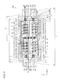
- FIG. 1 is a schematic plan view of the semiconductor device according to the first embodiment as viewed in the thickness direction of the substrate.
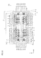
- FIG. 2 is a schematic plan view showing only the substrate and the circuit pattern included in the semiconductor device shown in FIG.
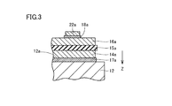
- FIG. 3 is a schematic cross-sectional view showing a part of the semiconductor device shown in FIG.
- FIG. 4 is a schematic plan view illustrating the flow of current flowing in the first state in the semiconductor device according to the first embodiment shown in FIG.
- FIG. 5 is a schematic plan view illustrating the flow of current flowing in the second state in the semiconductor device according to the first embodiment shown in FIG.
- FIG. 6 is an enlarged view of a part of the semiconductor device shown in FIG. FIG.
- FIG. 7 is a schematic plan view of the semiconductor device according to the second embodiment as viewed in the thickness direction of the substrate.
- FIG. 8 is a schematic plan view of the semiconductor device according to the third embodiment as viewed in the thickness direction of the substrate.
- FIG. 9 is a schematic plan view of the semiconductor device according to the fourth embodiment as viewed in the thickness direction of the substrate.
- FIG. 10 is a schematic plan view illustrating the flow of current flowing in the forward direction in the semiconductor device according to the fourth embodiment shown in FIG.
- FIG. 11 is a schematic plan view illustrating the flow of current flowing in the opposite direction in the semiconductor device according to the fourth embodiment shown in FIG.
- FIG. 12 is a schematic plan view of the semiconductor device according to the fifth embodiment as viewed in the thickness direction of the substrate.
- one of the purposes is to provide a semiconductor device capable of facilitating control for obtaining an output close to a desired AC waveform.
- the semiconductor device includes an insulating substrate, a circuit pattern arranged on the substrate, a P terminal, an N terminal and an O terminal electrically connected to the circuit pattern, and a third mounted on the circuit pattern. It includes a 1-transistor chip and a 2nd transistor chip, and a 1st diode chip and a 2nd diode chip mounted on a circuit pattern.
- the circuit pattern is electrically connected to the P terminal and extends along the first direction in a band-shaped first region, and is electrically connected to the N terminal in the second direction which is the width direction of the first region.
- a third region is included.
- the third region is arranged with a band-shaped first branch extending along the first direction and a band-shaped second branch extending along the first direction at intervals from the first branch in the second direction.
- the first transistor chip is mounted in the first region and electrically connected to the first region, and is electrically connected to the first branch portion by the first wiring.
- the second transistor chip is mounted on the second branch portion and electrically connected to the second branch portion, and is electrically connected to the second region by the second wiring.
- the first diode chip is mounted in the first region and electrically connected to the first region, and is electrically connected to the first branch portion by a connecting member.
- the second diode chip is mounted on the second branch portion and electrically connected to the second branch portion, and is electrically connected to the second region by the connecting member.
- the first transistor chip and the first diode chip are arranged side by side along the first direction.
- the second transistor chip and the second diode chip are arranged side by side along the first direction.
- the present inventors have studied a configuration of a semiconductor device capable of facilitating control for obtaining an output close to a desired AC waveform, and have come up with the following configuration.
- the P terminal is in the first state when the electrical connection between the P terminal and the O terminal is on and the electrical connection between the O terminal and the N terminal is off. Current flows from the circuit pattern, the transistor chip in the on state, and the circuit pattern again to the O terminal. Further, in the second state where the electrical connection between the P terminal and the O terminal is off and the electrical connection between the O terminal and the N terminal is on, the circuit pattern is displayed from the O terminal. , The transistor chip in the on state, and the current flows to the N terminal again through the circuit pattern.
- the current flows in the region where the transistor chips are mounted in the transistor chips that are in the off state among the plurality of transistor chips.
- the circuit pattern generates heat due to this current flow.
- heat dissipation from the transistor chip is hindered.
- a difference in cooling rate occurs between the transistor chip arranged in the region where the current flows in the circuit pattern and the transistor chip arranged in the region where the current does not flow.
- the temperature difference between the plurality of transistor chips becomes large, and electrical control for obtaining an output close to a desired AC waveform becomes complicated during high-speed switching operation. Therefore, in the first state and the second state, it is considered to separate the path through which the current flows in the circuit pattern, respectively.
- the semiconductor device of the present disclosure in the first state, the first region of the circuit pattern from the P terminal, the first transistor chip in the on state, the first wiring, and the first branch portion of the third region of the circuit pattern. Then, a current flows through the connection portion in the third region of the circuit pattern to the O terminal. At this time, no current flows through the second branch portion of the third region of the circuit pattern on which the second transistor chip that is in the off state is mounted. Then, in the first state, it is possible to prevent the heat dissipation of the second transistor chip from being hindered by the heat generated by the second branch portion of the third region of the circuit pattern.
- the connection portion of the third region of the circuit pattern from the O terminal, the second branch portion of the third region of the circuit pattern, the second transistor chip in the on state, the second wiring, and the circuit pattern A current flows through the second region of the N terminal. At this time, no current flows in the first region of the circuit pattern on which the first transistor chip that is in the off state is mounted. Then, in the second state, it is possible to suppress the heat dissipation of the first transistor chip from being hindered by the heat generation in the first region of the circuit pattern. In this way, the path of the current flowing through the circuit pattern is separated between the first state and the second state.
- the difference between the cooling rate of the first transistor chip and the cooling rate of the second transistor chip when they are in the off state can be reduced. Therefore, in such a semiconductor device, the temperature difference between the first transistor chip and the second transistor chip can be reduced. Therefore, it is possible to facilitate electrical control for obtaining an output close to a desired AC waveform.
- the first transistor chip and the first diode chip are arranged side by side along the first direction, and the second transistor chip and the second diode chip are arranged in the first direction.
- Adopt a configuration in which they are arranged side by side along. By doing so, it is possible to reduce the density of the transistor chips and diode chips, which are heat sources, and promote the homogenization of heat. Therefore, the effect of reducing the temperature difference between the transistor chip and the diode chip can be further obtained. In particular, when a copper plate having high thermal conductivity is used as the circuit pattern, this effect can be remarkably obtained. Further, with such a configuration, it is possible to avoid an increase in the size of the semiconductor device in the second direction. Such a configuration leads to minimizing the wiring routing when connecting a plurality of such semiconductor devices side by side in parallel.
- the first region is divided into a one-sided first region arranged on one side in the first direction and a other-side first region arranged on the other side, and arranged side by side in the first direction.
- the divided portions may be electrically connected by a connecting member.
- the second region is divided into a second region on one side arranged on one side in the first direction and a second region on the other side arranged on the other side, arranged side by side in the first direction, and divided.
- the portions may be electrically connected by a connecting member.
- the first branch portion is divided into a first branch portion on one side arranged on one side in the first direction and a first branch portion on the other side arranged on the other side, and arranged side by side in the first direction.
- the divided portions may be electrically connected by a connecting member.
- the second branch portion is divided into a second branch portion on one side arranged on one side in the first direction and a second branch portion on the other side arranged on the other side, and arranged side by side in the first direction.
- the divided portions may be electrically connected by a connecting member.
- the semiconductor device may further include a plurality of third diode chips and a plurality of fourth diode chips mounted in a circuit pattern.
- the plurality of third diode chips are adjacent to each other along the first direction, arranged side by side with the first diode chip in the second direction, mounted in the first region, and electrically connected to the first region.
- And may be electrically connected to the first branch portion by a connecting member.
- Each of the plurality of fourth diode chips is adjacent to each other along the first direction, is arranged side by side with the third diode chip in the second direction, is mounted on the second branch portion, and is electrically mounted on the second branch portion. It may be connected and electrically connected to the second region by a connecting member.
- a plurality of first transistor chips may be provided.
- a plurality of second transistor chips may be provided.
- a plurality of first diode chips may be provided.
- a plurality of second diode chips may be provided.
- the plurality of first transistor chips may be arranged next to each other along the first direction.
- the plurality of second transistor chips may be arranged next to each other along the first direction.
- the plurality of first diode chips may be arranged next to each other along the first direction.
- the plurality of second diode chips may be arranged next to each other along the first direction.
- a plurality of first transistor chips may be mounted on one side first region.
- the plurality of first diode chips may be mounted on the first region on the other side.
- the plurality of second transistor chips may be mounted on the second branch on the other side.
- the plurality of second diode chips may be mounted on the second branch on one side.
- a plurality of third diode chips may be mounted on the first region on the other side.
- the plurality of fourth diode chips may be mounted on the second branch on one side.
- a plurality of first transistor chips may be provided.
- a plurality of second transistor chips may be provided.
- a plurality of first diode chips may be provided.
- a plurality of second diode chips may be provided.
- the plurality of first transistor chips and the plurality of first diode chips may be arranged side by side alternately along the first direction.
- the plurality of second transistor chips and the plurality of second diode chips may be arranged side by side alternately along the first direction.
- Transistor chips and diode chips generate heat differently depending on operating conditions, control conditions, and operating conditions. However, by arranging the transistor chips and the diode chips alternately in the first direction in this way, it is possible to further make the heat generation uniform.
- a heat radiating plate having one surface in the thickness direction on which the substrate is mounted and a frame body that rises from the one surface and is arranged so as to surround the substrate in the thickness direction of the substrate are further provided.
- the outer shape of the substrate may be a rectangle whose long side extends in the first direction when viewed in the thickness direction of the substrate.
- the frame may include a first wall portion and a second wall portion corresponding to a pair of long sides of the substrate, respectively.
- the P terminal and the N terminal may be arranged on the side opposite to the second short side when viewed from the first short side of the substrate.
- the O terminal may be arranged on the side opposite to the first short side when viewed from the second short side.
- a second gate terminal connected to the device may be further provided.
- the distance between the first wall and the first region is the distance between the first wall and the second region, the distance between the first wall and the first branch, and It may be smaller than any of the distances between the first wall portion and the second branch portion.
- the distance between the second wall and the second branch is the distance between the second wall and the first region, the distance between the second wall and the second region, and It may be smaller than any of the distances between the second wall portion and the first branch portion.
- the distance between the first wall and the first region is the distance between the first wall and the second region, the distance between the first wall and the first branch, and It may be smaller than any of the distances between the first wall portion and the second branch portion.
- the distance between the second wall and the second branch is the distance between the second wall and the first region, the distance between the second wall and the second region, and It may be smaller than any of the distances between the second wall portion and the first branch portion.
- the first gate terminal and the first Kelvin source terminal may be mounted adjacent to the first wall portion.
- the second gate terminal and the second Kelvin source terminal may be mounted adjacent to the second wall portion.
- the circuit pattern is electrically connected to the first Kelvin source terminal by a connecting member, is arranged at intervals from the first region in the second direction, and has a strip-shaped fourth region extending along the first direction.
- a band-shaped fifth region that is electrically connected to the first gate terminal by a connecting member, is arranged at intervals from the fourth region in the second direction, and extends along the first direction, and a second region by the connecting member.
- a band-shaped sixth region that is electrically connected to the gate terminal and is spaced apart from the second branch in the second direction and extends along the first direction, and a second Kelvin source terminal by a connecting member. It may further include a strip-shaped seventh region that is electrically connected, spaced apart from the sixth region in the second direction, and extends along the first direction.
- the direction of the current from the first gate terminal to the gate pad of the first transistor chip in the fifth region is opposite to the direction of the current from the Kelvin source pad of the first transistor chip to the first Kelvin source terminal in the fourth region. It may be oriented.
- the direction of the current from the second gate terminal to the gate pad of the second transistor chip in the sixth region is opposite to the direction of the current from the Kelvin source pad of the second transistor chip to the second Kelvin source terminal in the seventh region. It may be oriented. By doing so, when a current flows in the current path composed of the first gate terminal, the fifth region of the circuit pattern, the first transistor chip, the fourth region of the circuit pattern, and the first Kelvin source terminal, the first The direction of the flowing current can be reversed between the fourth region and the fifth region, which are arranged at intervals in the two directions.
- the first wiring may include a first source connecting member that electrically connects the source pad of the first transistor chip and the first branch portion.
- the second wiring may include a second source connecting member that electrically connects the source pad of the second transistor chip and the second region.
- the length of the first source connecting member and the length of the second source connecting member may be the same.
- the number of the first source connecting member and the number of the second source connecting member may be the same.
- At least one of the first transistor chip and the second transistor chip may include a semiconductor layer made of SiC or GaN. Since the transistor chip including such a semiconductor layer can be switched at high speed, it is suitable for the semiconductor device of the present disclosure which is premised on switching the current path.
- the first branch portion may be arranged between the first region and the second region in the second direction.
- the second region may be arranged between the first branch and the second branch in the second direction.
- FIG. 1 is a schematic plan view of the semiconductor device according to the first embodiment as viewed in the thickness direction of the substrate.
- FIG. 2 is a schematic plan view showing only the substrate and the circuit pattern included in the semiconductor device shown in FIG. In FIG. 1 and the like, the boundary between the first branch portion and the connecting portion and the boundary between the second branch portion and the connecting portion, which will be described later, are indicated by broken lines.
- FIG. 3 is a schematic cross-sectional view showing a part of the semiconductor device shown in FIG.
- FIG. 3 is a cross-sectional view of the case where the first transistor chip is included and cut along a plane parallel to the XX plane.
- the semiconductor device 11a includes a heat radiating plate 12, a frame body 13, a metal plate 14a (see FIG. 3), a substrate 15a, and a circuit pattern 16a.
- the solder portions 17a, 18a see FIG. 3
- the P terminal 19a, the O terminals 19b, 19c, the N terminal 19d, the first diode chips 21a, 21b, 21c, 21d, and the first transistor chip 22a It includes 22b, 22c, 22d, second diode chips 21e, 21f, 21g, 21h, and second transistor chips 22e, 22f, 22g, 22h.
- the heat radiating plate 12 is made of metal.
- the heat radiating plate 12 is made of copper, for example.
- the surface of the heat radiating plate 12 may be nickel-plated.
- the outer shape of the heat radiating plate 12 is a rectangle in which the side extending in the X direction is the long side and the side extending in the Y direction is the short side when viewed in the thickness direction, and the corners are curved surfaces.
- the solder portion 17a is arranged on one surface 12a of the heat radiating plate 12 in the thickness direction.
- As the material of the solder portion 17a for example, Sn-Ag-Cu-based solder or Sn-Sb-based solder is used.
- the metal plate 14a is arranged on the solder portion 17a.
- the heat radiating plate 12 and the metal plate 14a are joined by the solder portion 17a.
- the metal plate 14a is made of, for example, copper.
- the substrate 15a is arranged on the metal plate 14a.
- the substrate 15a is mounted on one surface 12a of the heat radiating plate 12.
- the substrate 15a is insulating. Examples of the material of the insulating substrate 15a include Al 2 O 3 , Al N, and Si 3 N 4 .
- the thickness direction of the heat radiating plate 12 and the thickness direction of the substrate 15a are both in the Z direction.
- the outer shape of the substrate 15a is a rectangle whose long side extends in the X direction, which is the first direction described later, when viewed in the thickness direction of the substrate 15a. Specifically, with reference to FIG. 2, the outer shape of the substrate 15a is composed of a pair of long sides 33a and 33b and a pair of short sides 34a and 34b when viewed in the thickness direction of the substrate 15a. ..
- the circuit pattern 16a is arranged on the substrate 15a.
- the circuit pattern 16a is made of, for example, copper. The specific configuration of the circuit pattern 16a will be described in detail later.
- the frame body 13 rises from one surface 12a of the heat radiating plate 12 and is arranged so as to surround the substrate 15a when viewed in the thickness direction of the substrate 15a.
- the frame body 13 includes a first wall portion 13a, a second wall portion 13b, a third wall portion 13c, and a fourth wall portion 13d.
- the first wall portion 13a and the second wall portion 13b are arranged so as to face each other in the Y direction.
- the third wall portion 13c and the fourth wall portion 13d are arranged so as to face each other in the X direction.
- the frame body 13 is made of, for example, an insulating resin.
- the frame body 13 is fixed to the heat radiating plate 12 with, for example, an adhesive.
- the heat radiating plate 12 and the frame 13 form a case 20 included in the semiconductor device 11a.
- the space 30 inside the case 20 is filled with a resin filler (not shown).
- the P terminal 19a, the O terminal 19b, 19c and the N terminal 19d are plate-shaped and made of metal, respectively.
- the P terminal 19a, the O terminal 19b, 19c, and the N terminal 19d each have a bent band shape.
- the P terminal 19a, the O terminal 19b, 19c and the N terminal 19d are formed by bending, for example, a strip-shaped copper plate, respectively.
- the P terminal 19a and the N terminal 19d are arranged on one side of the substrate 15a where the third wall portion 13c is located, and the O terminals 19b and 19c sandwich the substrate 15a. It is arranged on the other side where the fourth wall portion 13d is located.
- the P terminal 19a and the N terminal 19d are arranged on the side opposite to the second short side 34b when viewed from the first short side 34a of the substrate 15a.
- the O terminals 19b and 19c are arranged on the side opposite to the first short side 34a when viewed from the second short side 34b.
- the O terminals 19b and 19c are attached to the fourth wall portion 13d.
- the P terminal 19a and the N terminal 19d are attached to the third wall portion 13c.
- the semiconductor device 11a secures an electrical connection with the outside by means of P terminals 19a, O terminals 19b, 19c, and N terminals 19d.
- the direction from one side where the P terminal 19a and the N terminal 19d are arranged toward the O terminals 19b and 19c is indicated by the direction indicated by the arrow X in FIG.
- the first direction is the X direction indicated by the direction indicated by the arrow X or vice versa.
- the P terminal 19a, the O terminal 19b, 19c, and the N terminal 19d each have a portion exposed from the inner wall surface 27 of the frame body 13 to the space 30 side inside the case 20. Using this portion, each wire as a connecting member is electrically connected.
- the first diode chips 21a, 21b, 21c, 21d, the second diode chips 21e, 21f, 21g, 21h, the first transistor chips 22a, 22b, 22c, 22d and the second transistor chips 22e, 22f, 22g, 22h are SiC. Alternatively, it includes a semiconductor layer made of GaN.
- the first diode chips 21a, 21b, 21c, 21d and the second diode chips 21e, 21f, 21g, 21h are, for example, Schottky barrier diodes (SBDs).
- the first transistor chips 22a, 22b, 22c, 22d and the second transistor chips 22e, 22f, 22g, 22h are, for example, metal-oxide-semiconductor field effect transistors (MOSFETs).
- the first transistor chip 22a is mounted on the circuit pattern 16a.
- the first transistor chip 22a is electrically joined to the circuit pattern 16a by the solder portion 18a.
- the first transistor chip 22a includes a drain electrode located at one end of the substrate 15a in the thickness direction, and a source pad, a gate pad, and a Kelvin source pad located at the other end of the substrate 15a in the thickness direction. And, including.
- the first transistor chip 22a is joined to the circuit pattern 16a by the solder portion 18a so that the drain electrode is in contact with the circuit pattern 16a.
- a current flows through the first transistor chip 22a in the thickness direction of the substrate 15a.
- the first transistor chip 22a is a vertical transistor chip. The same applies to the configurations of the other first transistor chips 22b to 22d and the second transistor chips 22e to 22h.
- the first diode chip 21a is mounted on the circuit pattern 16a.
- the first diode chip 21a is electrically bonded to the circuit pattern 16a by the solder portion, similarly to the first transistor chip 22a.
- the first diode chip 21a includes a cathode pad located at one end of the substrate 15a in the thickness direction and an anode pad located at the other end of the substrate 15a in the thickness direction.
- the first diode chip 21a is joined to the circuit pattern 16a by the solder portion so that the cathode pad comes into contact with the circuit pattern 16a.
- a current flows through the first diode chip 21a in the thickness direction of the substrate 15a. The same applies to the configurations of the other first diode chips 21b to 21d and the second diode chips 21e to 21h.
- the semiconductor device 11a includes a first gate terminal 41a, a second gate terminal 41b, a first Kelvin source terminal 42a, a second Kelvin source terminal 42b, a D terminal 43, and thermistor terminals 44a and 44b.
- the first gate terminal 41a, the first Kelvin source terminal 42a, the D terminal 43, and the thermistor terminals 44a, 44b are attached to the first wall portion 13a at intervals in the X direction, respectively. Specifically, from the side closer to the fourth wall portion 13d, the order is D terminal 43, first Kelvin source terminal 42a, first gate terminal 41a, and thermistor terminals 44a, 44b.
- the second gate terminal 41b and the second Kelvin source terminal 42b are attached to the second wall portion 13b, respectively.
- first gate terminal 41a, the second gate terminal 41b, the first Kelvin source terminal 42a, the second Kelvin source terminal 42b, the D terminal 43, and the thermistor terminals 44a, 44b are exposed in the internal space 30. It is attached. Further, the first gate terminal 41a, the second gate terminal 41b, the first Kelvin source terminal 42a, the second Kelvin source terminal 42b, the D terminal 43, and the thermistor terminals 44a and 44b each secure an electrical connection with the outside. Therefore, it has a portion protruding from the upper surface of the frame body 13.
- the circuit pattern 16a includes a first region 51a, a second region 52a, a third region 53a, a fourth region 54a, a fifth region 55a, a sixth region 56a, a seventh region 57a, and an eighth region. It includes 58a and a ninth region 59a.
- the first region 51a, the second region 52a, the fourth region 54a, the fifth region 55a, the sixth region 56a, and the seventh region 57a are each strip-shaped and extend in the first direction.
- the third region 53a includes a first branch portion 61a, a second branch portion 62a, and a connection portion 63a.
- the first branch portion 61a and the second branch portion 62a are each strip-shaped and extend in the first direction.
- the connecting portion 63a is also strip-shaped.
- the connecting portion 63a extends in the second direction, which is the width direction of the first region 51a.
- the second direction is the Y direction indicated by the direction indicated by the arrow Y or vice versa.
- the connection portion 63a is an end portion on one side of the first branch portion 61a, in this case, an end portion on the side close to the fourth wall portion 13d, and an end portion on one side of the second branch portion 62a, in this case, the fourth. It is connected to the end portion on the side closer to the wall portion 13d.
- the eighth region 58a and the ninth region 59a each have a rectangular shape when viewed in the thickness direction of the substrate 15a.
- the eighth region 58a and the ninth region 59a are arranged side by side with an interval in the X direction when viewed in the thickness direction of the substrate 15a.
- the thermistor 28 included in the semiconductor device 11a is arranged so as to straddle the eighth region 58a and the ninth region 59a when viewed in the thickness direction of the substrate 15a.
- the thermistor 28 is electrically connected to the eighth region 58a and the ninth region 59a.
- the first region 51a, the second region 52a, the fourth region 54a, the fifth region 55a, the sixth region 56a, the seventh region 57a, the first branch portion 61a, and the second branch portion 62a are spaced apart from each other in the second direction. Is placed open.
- the first branch portion 61a is arranged between the first region 51a and the second region 52a.
- the second region 52a is arranged between the first branch portion 61a and the second branch portion 62a.
- the fourth region 54a, the fifth region 55a, the first region 51a, the first branch portion 61a, The second region 52a, the second branch portion 62a, the sixth region 56a, and the seventh region 57a are arranged in this order.
- the widths of the fourth region 54a, the fifth region 55a, the sixth region 56a, and the seventh region 57a are smaller than the widths of the first region 51a and the second region 52a, respectively.
- the distance between the first wall portion 13a and the first region 51a is the distance between the first wall portion 13a and the second region 52a, and the distance between the first wall portion 13a and the first branch portion 61a. It is smaller than either the distance between the first wall portion 13a and the second branch portion 62a. Further, in the second direction, the distance between the second wall portion 13b and the second branch portion 62a is the distance between the second wall portion 13b and the first region 51a, and the distance between the second wall portion 13b and the second. It is smaller than either the distance between the region 52a and the distance between the second wall portion 13b and the first branch portion 61a.
- the first diode chips 21a, 21b, 21c, 21d are arranged on the first region 51a.
- the first transistor chips 22a, 22b, 22c, 22d are arranged on the first region 51a.
- the first diode chips 21a to 21d and the first transistor chips 22a to 22d are arranged at intervals in the X direction, respectively.
- the first transistor chip 22a is arranged between the first diode chip 21a and the first diode chip 21b.
- the first transistor chip 22b is arranged between the first diode chip 21b and the first diode chip 21c.
- the first transistor chip 22c is arranged between the first diode chip 21c and the first diode chip 21d.
- the first transistor chip 22d is arranged in the X direction at a position opposite to the position where the first transistor chip 22c is arranged with respect to the first diode chip 21d. That is, the first transistor chips 22a, 22b, 22c, 22d and the first diode chips 21a, 21b, 21c, 21d are arranged alternately along the first direction.
- the distance between the first transistor chip 22b and the first diode chip 21c in the X direction is larger than the distance between the first transistor chip 22b and the first diode chip 21b in the X direction.
- the second diode chips 21e, 21f, 21g, 21h are arranged on the second branch portion 62a.
- the second transistor chips 22e, 22f, 22g, 22h are arranged on the second branch portion 62a.
- the second diode chips 21e to 21h and the second transistor chips 22e to 22h are arranged at intervals in the X direction, respectively.
- the second transistor chip 22e is arranged between the second diode chip 21e and the second diode chip 21f.
- the second transistor chip 22f is arranged between the second diode chip 21f and the second diode chip 21g.
- a second transistor chip 22g is arranged between the second diode chip 21g and the second diode chip 21h.
- the second transistor chip 22h is arranged in the X direction at a position opposite to the position where the second transistor chip 22g is arranged with respect to the second diode chip 21h. That is, the second transistor chips 22e, 22f, 22g, 22h and the second diode chips 21e, 21f, 21g, 21h are arranged alternately along the first direction.
- the distance between the second transistor chip 22f and the second diode chip 21g in the X direction is larger than the distance between the second transistor chip 22f and the second diode chip 21f in the X direction.
- the semiconductor device 11a includes a first wiring that electrically connects the first transistor chips 22a, 22b, 22c, 22d and the circuit pattern 16a.
- the first wiring is a wire 25a, 25b, 25c, 25d as a first source wire which is a first source connecting member for electrically connecting the first transistor chips 22a, 22b, 22c, 22d and the first branch portion 61a.
- the semiconductor device 11a includes a second wiring that electrically connects the second transistor chips 22e, 22f, 22g, 22h and the circuit pattern 16a.
- the second wiring includes wires 25e, 25f, 25g, 25h as a second source wire, which is a second source connecting member that electrically connects the second transistor chips 22e, 22f, 22g, 22h and the second region 52a.
- the semiconductor device 11a includes wires 23a, 23b, 23c, 23d, 24a, 24b, 24c, 24d, 24e, 24f, 24g, 24h, 26a, 26b, 26c, 26d, 26e, 26f, 26g, as connecting members.
- the P terminal 19a and the first region 51a are electrically connected by a wire 23a.
- the O terminal 19b and the connecting portion 63a are electrically connected by a wire 23b.
- the O terminal 19c and the connecting portion 63a are electrically connected by a wire 23c.
- the third region 53a including the connection portion 63a has the same potential as the O terminals 19b and 19c.
- the N terminal 19d and the second region 52a are electrically connected by a wire 23d.
- the anode pads of the first diode chips 21a, 21b, 21c, and 21d and the first branch portion 61a are electrically connected by wires 24a, 24b, 24c, and 24d, respectively.
- the source pads of the first transistor chips 22a, 22b, 22c, and 22d and the first branch portion 61a are electrically connected by wires 25a, 25b, 25c, and 25d, respectively.
- the gate pads of the first transistor chips 22a, 22b, 22c, and 22d and the fifth region 55a are electrically connected by wires 31a, 31c, 31e, and 31g, respectively.
- the Kelvin source pads of the first transistor chips 22a, 22b, 22c, and 22d and the fourth region 54a are electrically connected by wires 31b, 31d, 31f, and 31h, respectively.
- the fifth region 55a and the first gate terminal 41a are electrically connected by a wire 26c.
- the fourth region 54a and the first Kelvin source terminal 42a are electrically connected by a wire 26b.
- the fourth region 54a, the fifth region 55a, the first gate terminal 41a, and the first Kelvin source terminal 42a form a part of the control circuit that controls the operation of the first transistor chips 22a, 22b, 22c, 22d. do.
- the first region 51a and the D terminal 43 are electrically connected by a wire 26a.
- the eighth region 58a and the thermistor terminal 44a are electrically connected by a wire 26d.
- the ninth region 59a and the thermistor terminal 44b are electrically connected by a wire 26e.
- the anode pads of the second diode chips 21e, 21f, 21g, and 21h and the second region 52a are electrically connected by wires 24e, 24f, 24g, and 24h, respectively.
- the source pads of the second transistor chips 22e, 22f, 22g, and 22h and the second region 52a are electrically connected by wires 25e, 25f, 25g, and 25h, respectively.
- the gate pads of the second transistor chips 22e, 22f, 22g, and 22h and the sixth region 56a are electrically connected by wires 32a, 32c, 32e, and 32g, respectively.
- the Kelvin source pads of the second transistor chips 22e, 22f, 22g, and 22h and the seventh region 57a are electrically connected by wires 32b, 32d, 32f, and 32h, respectively.
- the sixth region 56a and the second gate terminal 41b are electrically connected by a wire 26f.
- the seventh region 57a and the second Kelvin source terminal 42b are electrically connected by a wire 26g.
- the sixth region 56a, the seventh region 57a, the second gate terminal 41b, and the second Kelvin source terminal 42b form a part of the control circuit that controls the operation of the second transistor chips 22e, 22f, 22g, 22h. do.
- the first region 51a and the D terminal 43 are electrically connected by a wire 26a.
- FIG. 4 is a schematic plan view illustrating the flow of the current flowing in the first state in the semiconductor device 11a according to the first embodiment shown in FIG. 4 shows a flow of current, from the P terminal 19a to the O terminal 19b by the arrow D 1.
- FIG. 5 is a schematic plan view illustrating the flow of current flowing in the second state in the semiconductor device 11a according to the first embodiment shown in FIG. 5 shows a flow of current, from O terminal 19c to the N terminal 19d by the arrow D 2.
- the first transistor chips 22a, 22b, 22c, 22d are turned on, the electrical connection between the P terminal 19a and the O terminal 19b is turned on, and the O terminal 19c
- the wires 23a from the P terminal 19a, the first region 51a of the circuit pattern 16a, the first transistor chips 22a, 22b in the on state, 22c, 22d, the first wiring wires 25a, 25b, 25c, 25d, the first branch portion 61a of the third region 53a of the circuit pattern 16a, the connection portion 63a of the third region 53a of the circuit pattern 16a, and the wire 23b.
- a current flows through the O terminal 19b.
- the path of the current flowing through the circuit pattern 16a is separated between the first state and the second state. Then, the difference between the cooling rates of the first transistor chips 22a, 22b, 22c, and 22d and the cooling rates of the second transistor chips 22e, 22f, 22g, and 22h when they are in the off state can be reduced. Therefore, such a semiconductor device 11a can reduce the temperature difference between the first transistor chips 22a, 22b, 22c, 22d and the second transistor chips 22e, 22f, 22g, 22h. Therefore, it is possible to facilitate electrical control for obtaining an output close to a desired AC waveform.
- the semiconductor device 11a has a heat radiating plate 12 having one surface 12a in the thickness direction on which the substrate 15a is mounted, and the substrate 15a rising from the one surface 12a and viewed in the thickness direction of the substrate 15a.
- the outer shape of the substrate 15a is a rectangle whose long side extends in the first direction when viewed in the thickness direction of the substrate 15a.
- the frame body 13 includes a first wall portion 13a and a second wall portion 13b corresponding to a pair of long sides of the substrate 15a, respectively.
- the P terminal 19a and the N terminal 19d are arranged on the side opposite to the second short side when viewed from the first short side of the substrate 15a.
- the O terminals 19b and 19c are arranged on the side opposite to the first short side when viewed from the second short side. Therefore, it is a semiconductor device that can easily achieve the structure of the semiconductor device 11a.
- the semiconductor device 11a has a first gate terminal 41a attached to the first wall portion 13a and electrically connected to the gate pads of the first transistor chips 22a, 22b, 22c, 22d, and a second gate terminal 41a. It includes a second gate terminal 41b attached to the wall portion 13b and electrically connected to the gate pad of the second transistor chips 22e, 22f, 22g, 22h. Further, in the second direction, the distance between the first wall portion 13a and the first region 51a is the distance between the first wall portion 13a and the second region 52a, and the distance between the first wall portion 13a and the first branch. It is smaller than either the distance between the portion 61a and the distance between the first wall portion 13a and the second branch portion 62a.
- the distance between the second wall portion 13b and the second branch portion 62a is the distance between the second wall portion 13b and the first region 51a, and the distance between the second wall portion 13b and the second region 52a. It is smaller than either the distance between the second wall portion 13b and the first branch portion 61a. Therefore, such a semiconductor device 11a has a length of wires 31a, 31c, 31e, 31g and a number of wires 31a, 31c, 31e, 31g which are wirings for connecting the first gate terminal 41a and the gate pads of the first transistor chips 22a, 22b, 22c, 22d.
- the lengths of the wires 32a, 32c, 32e, and 32g which are the wirings connecting the two gate terminals 41b and the gate pads of the second transistor chips 22e, 22f, 22g, and 22h, can be shortened, respectively. Therefore, the inductance can be reduced.
- the semiconductor device 11a has a first Kelvin source terminal 42a attached to the first wall portion 13a and electrically connected to the Kelvin source pad of the first transistor chips 22a, 22b, 22c, 22d, and a second wall portion 13b. Includes a second Kelvin source terminal 42b, which is attached to and electrically connected to the Kelvin source pad of the second transistor chips 22e, 22f, 22g, 22h. Further, in the second direction, the distance between the first wall portion 13a and the first region 51a is the distance between the first wall portion 13a and the second region 52a, and the distance between the first wall portion 13a and the first branch. It is smaller than either the distance between the portion 61a and the distance between the first wall portion 13a and the second branch portion 62a.
- the distance between the second wall portion 13b and the second branch portion 62a is the distance between the second wall portion 13b and the first region 51a, and the distance between the second wall portion 13b and the second region 52a. It is smaller than either the distance between the second wall portion 13b and the first branch portion 61a. Therefore, such a semiconductor device 11a has a length of wires 31b, 31d, 31f, 31h, which are wirings for connecting the first Kelvin source terminal 42a and the Kelvin source pads of the first transistor chips 22a, 22b, 22c, 22d.
- the lengths of the wires 32b, 32d, 32f, and 32h which are the wirings connecting the second Kelvin source terminal 42b and the Kelvin source pads of the second transistor chips 22e, 22f, 22g, and 22h, can be shortened, respectively. Therefore, the inductance can be reduced.
- the semiconductor device 11a is a wire 25a, 25b, 25c which is a first source wire for electrically connecting the source pad of the first transistor chips 22a, 22b, 22c, 22d and the first branch portion 61a.
- 25d, and wires 25e, 25f, 25g, 25h which are second source wires that electrically connect the source pads of the second transistor chips 22e, 22f, 22g, 22h and the second region 52a.
- the lengths of the wires 25a, 25b, 25c, 25d and the lengths of the wires 25e, 25f, 25g, 25h are the same.
- the number of wires 25a, 25b, 25c, 25d and the number of wires 25e, 25f, 25g, 25h are the same. Therefore, such a semiconductor device 11a can easily make the values of inductance in each electrical path uniform. Therefore, the electrical characteristics of each route can be easily aligned, and electrical control can be facilitated.
- At least one of the first transistor chips 22a, 22b, 22c, 22d and the second transistor chips 22e, 22f, 22g, 22h includes a semiconductor layer made of SiC or GaN. Since the transistor chip including such a semiconductor layer can be switched at high speed, it is suitable for the semiconductor device of the present disclosure which is premised on switching the current path.
- the first gate terminal 41a and the first Kelvin source terminal 42a are attached adjacent to the first wall portion 13a.
- the second gate terminal 41b and the second Kelvin source terminal 42b are attached adjacent to the second wall portion 13b.
- the circuit pattern 16a is electrically connected to the first Kelvin source terminal 42a by a wire 26b, is arranged at intervals from the first region 51a in the second direction, and has a strip-shaped fourth extending along the first direction.
- the region 54a is electrically connected to the first gate terminal 41a by a wire 26c, is arranged at a distance from the fourth region 54a in the second direction, and has a strip-shaped fifth region 55a extending along the first direction.
- band-shaped sixth region 56a which is electrically connected to the second gate terminal 41b by the wire 26f, is arranged at a distance from the second branch portion 62a in the second direction, and extends along the first direction.
- FIG. 6 is an enlarged view of a part of the semiconductor device 11a shown in FIG.
- the direction of the current from the first gate terminal 41a to the gate pads of the first transistor chips 22a, 22b, 22c, 22d in the fifth region 55a and the direction of the current from the first transistor chip 22a in the fourth region 54a The direction of the current from the Kelvin source pads 22b, 22c, 22d to the first Kelvin source terminal 42a is opposite to that of the current.
- the direction of the current from the Kelvin source pad of the chips 22e, 22f, 22g, 22h to the second Kelvin source terminal 42b is opposite to that of the current direction.
- the arrow D 3 is composed of the first gate terminal 41a, the fifth region 55a of the circuit pattern 16a, the first transistor chip 22a, the fourth region 54a of the circuit pattern 16a, and the first Kelvin source terminal 42a.
- the current path is not shown, it is similarly composed of a second gate terminal 41b, a seventh region 57a of the circuit pattern 16a, a second transistor chip 22e, a sixth region 56a of the circuit pattern 16a, and a second Kelvin source terminal 42b.
- the direction of the flowing current can be reversed between the sixth region 56a and the seventh region 57a, which are arranged at intervals in the second direction. Therefore, it is possible to reduce the inductance in these control circuits by the mutual inductance of each.
- FIG. 7 is a schematic plan view of the semiconductor device according to the second embodiment as viewed in the thickness direction of the substrate.
- the semiconductor device of the second embodiment is different from the case of the first embodiment in that the substrate and the circuit pattern are divided.
- the substrate 15b included in the semiconductor device 11b according to the second embodiment is divided into a first substrate 80a and a second substrate 80b.
- the outer shape of the first substrate 80a and the outer shape of the second substrate 80b are rectangular when viewed in the thickness direction of the substrate 15b, respectively.
- the first substrate 80a and the second substrate 80b are arranged side by side at intervals in the X direction.
- the semiconductor device 11b according to the second embodiment includes wires 29a, 29b, 29c, 29d, 29e, 29f, 29g, 29h as connecting members.
- the circuit pattern 16b includes a first region 51b, 71b, a second region 52b, 72b, a third region 53b, a fourth region 54b, 74b, a fifth region 55b, 75b, and a sixth region. It includes regions 56b, 76b, seventh regions 57b, 77b, eighth regions 58b, and ninth regions 59b. Since the configurations of the eighth region 58b and the ninth region 59b are the same as those of the eighth region 58a and the ninth region 59a, their description will be omitted.
- the third region 53b includes first branch portions 61b and 81b, second branch portions 62b and 82b, and a connection portion 63b.
- the connection portion 63b is arranged.
- a first region 71b, a second region 72b, a fourth region 74b, a fifth region 75b, a sixth region 76b, a seventh region 77b, an eighth region 58b, and a ninth region 59b are arranged on the second substrate 80b. Will be done.
- the first regions 51b and 71b are divided into a first region 51b on one side arranged on one side in the first direction and a first region 71b on the other side arranged on the other side, and are arranged side by side in the first direction. Will be done.
- the second regions 52b and 72b are divided into a second region 52b on one side arranged on one side in the first direction and a second region 72b on the other side arranged on the other side, and are arranged side by side in the first direction. Will be done.
- the first branching portions 61b and 81b are divided into one side first branching portion 61b arranged on one side in the first direction and the other side first branching portion 81b arranged on the other side in the first direction. Arranged side by side.
- the second branch portions 62b and 82b are divided into one side second branch portion 62b arranged on one side in the first direction and the other side second branch portion 82b arranged on the other side in the first direction. Arranged side by side.
- the first region 51b on one side, the second region 52b on one side, the first branch portion 61b on one side, and the second branch portion 62b on one side are arranged on the O terminals 19b and 19c in the first direction, respectively.
- the other side first region 71b, the other side second region 72b, the other side first branch portion 81b, and the other side second branch portion 82b are arranged on the P terminal 19a side and the N terminal 19d side, respectively, in the first direction. ..
- the width of the first region 51b on one side that is, the length of the first region 51b on one side in the second direction
- the width of the first region 71b on the other side that is, the length of the first region 71b on the other side in the second direction. Is equal to.
- the width of the second region 52b on one side that is, the length of the second region 52b on one side in the second direction
- the width of the second region 72b on the other side that is, the length of the second region 72b on the other side in the second direction. Is equal to.
- the width of the first branch portion 61b on one side that is, the length of the first branch portion 61b on one side in the second direction
- the width of the first branch portion 81b on the other side that is, the second of the first branch portion 81b on the other side. Is equal to the length in the direction of.
- the width of the second branch portion 62b on the one side that is, the length of the second branch portion 62b on the one side in the second direction and the width of the second branch portion 82b on the other side, that is, the second of the second branch portion 82b on the other side. Is equal to the length in the direction of.
- the first diode chips 21a and 21b and the first transistor chips 22a and 22b are mounted in the first region 51b on one side.
- the first diode chips 21c and 21d and the first transistor chips 22c and 22d are mounted in the first region 71b on the other side.
- the second diode chips 21e and 21f and the second transistor chips 22e and 22f are mounted on the second branch portion 62b on one side.
- the second diode chips 21g and 21h and the second transistor chips 22g and 22h are mounted on the second branch portion 82b on the other side.
- the order of arrangement in the first direction is the same as in the case of the first embodiment.
- the divided parts are electrically connected by wires. Specifically, the first region 51b on the first substrate 80a and the first region 71b on the second substrate 80b are electrically connected by a wire 29a. The second region 52b on the first substrate 80a and the second region 72b on the second substrate 80b are electrically connected by a wire 29b. The fourth region 54b on the first substrate 80a and the fourth region 74b on the second substrate 80b are electrically connected by a wire 29c. The fifth region 55b on the first substrate 80a and the fifth region 75b on the second substrate 80b are electrically connected by a wire 29d. The sixth region 56b on the first substrate 80a and the sixth region 76b on the second substrate 80b are electrically connected by a wire 29e.
- the seventh region 57b on the first substrate 80a and the seventh region 77b on the second substrate 80b are electrically connected by a wire 29f.
- the first branch portion 61b on the first substrate 80a and the first branch portion 81b on the second substrate 80b are electrically connected by a wire 29g.
- the second branch portion 62b on the first substrate 80a and the second branch portion 82b on the second substrate 80b are electrically connected by a wire 29h.
- the first regions 51b and 71b, the second regions 52b and 72b, the first branch portions 61b and 81b and the second branch portions 62b and 82b are each divided in the first direction, and different substrates are used. It can be arranged on 80a and 80b. Therefore, the stress generated based on the difference in the coefficient of thermal expansion of each member can be relaxed.
- FIG. 8 is a schematic plan view of the semiconductor device according to the third embodiment as viewed in the thickness direction of the substrate.
- the arrangement of the circuit pattern arranged on the substrate is different from that of the first embodiment.
- the semiconductor device 11c includes a substrate 15c and a circuit pattern 16c arranged on the substrate 15c.
- the circuit pattern 16c arranged on the substrate 15c includes a first region 51c, a second region 52c, a third region 53c, a fourth region 54c, a fifth region 55c, a sixth region 56c, and a seventh region.
- the region 57c, the eighth region 58c, and the ninth region 59c are included. Since the configurations of the eighth region 58c and the ninth region 59c are the same as those of the eighth region 58a and the ninth region 59a, their description will be omitted.
- the third region 53c includes a first branch portion 61c, a second branch portion 62c, and a connection portion 63c.
- the second branch portion 62c is arranged between the first region 51c and the second region 52c in the second direction.
- the first region 51c is arranged between the first branch portion 61c and the second branch portion 62c.
- the second branch portion 62c, the second region 52c, the sixth region 56c, and the seventh region 57c are arranged in this order.
- the first transistor chips 22a to 22d and the second transistor chips 22e to 22h can be arranged in a region near the center of the heat radiating plate 12 when viewed in the thickness direction of the substrate 15a, so that heat is dissipated. The sex can be improved.
- FIG. 9 is a schematic plan view of the semiconductor device according to the fourth embodiment as viewed in the thickness direction of the substrate.
- the arrangement of the circuit pattern arranged on the substrate is different from that of the first embodiment.
- the substrate 15d included in the semiconductor device 11d according to the fourth embodiment is divided into a first substrate 80a and a second substrate 80b, similarly to the substrate 15b shown in the second embodiment. ing.
- the outer shape of the first substrate 80a and the outer shape of the second substrate 80b are rectangular when viewed in the thickness direction of the substrate 15d, respectively.
- the first substrate 80a and the second substrate 80b are arranged side by side at intervals in the X direction.
- the circuit pattern 16d includes a first region 51d, 71d, a second region 52d, 72d, a third region 53d, a fourth region 54d, a fifth region 55d, and a sixth region 76d.
- the seventh region 77d, the eighth region 58d, and the ninth region 59d are included. Since the configurations of the eighth region 58d and the ninth region 59d are the same as those of the eighth region 58a and the ninth region 59a, their description will be omitted.
- the third region 53d includes first branch portions 61d and 81d, second branch portions 62d and 82d, and a connection portion 63d.
- a first region 51d, a second region 52d, a fourth region 54d, a fifth region 55d, a first branch portion 61d, a second branch portion 62d, and a connection portion 63d are arranged on the first substrate 80a. That is, in the present embodiment, unlike the case of the second embodiment, the sixth region 76d and the seventh region 77d are not arranged on the first substrate 80a.
- a first region 71d, a second region 72d, a sixth region 76d, a seventh region 77d, an eighth region 58d, and a ninth region 59d are arranged on the second substrate 80b. That is, in the present embodiment, unlike the case of the second embodiment, the fourth region 54d and the fifth region 55d are not arranged on the second substrate 80b.
- the first regions 51d and 71d are divided into a first region 51d on one side arranged on one side in the first direction and a first region 71d on the other side arranged on the other side, and are arranged side by side in the first direction. Will be done.
- the fourth region 54d and the fifth region 55d are arranged next to the first region 51d on one side.
- the second regions 52d and 72d are divided into a second region 52d on one side arranged on one side in the first direction and a second region 72d on the other side arranged on the other side, and are arranged side by side in the first direction. Will be done.
- the first branching portions 61d and 81d are divided into one side first branching portion 61d arranged on one side in the first direction and the other side first branching portion 81d arranged on the other side in the first direction. Arranged side by side.
- the second branch portions 62d and 82d are divided into a one-sided second branch portion 62d arranged on one side in the first direction and a other-side second branch portion 82d arranged on the other side in the first direction. Arranged side by side. In the second direction, the sixth region 76d and the seventh region 77d are arranged next to the second branch portion 82d on the other side.
- the first region 51d on one side, the second region 52d on one side, the first branch portion 61d on one side, and the second branch portion 62d on one side are arranged on the O terminals 19b and 19c in the first direction, respectively.
- the other side first region 71d, the other side second region 72d, the other side first branch portion 81d, and the other side second branch portion 82d are arranged on the P terminal 19a side and the N terminal 19d side, respectively, in the first direction. ..
- the width of the first region 51d on one side is the width of the first region 71d on the other side, that is, the length of the first region 71d on the other side in the second direction. Shorter than the length.
- the length of the first region 71d on the other side in the second direction is such that two diode chips can be arranged side by side in the second direction.
- the width of the second region 52d on one side that is, the length of the second region 52d on one side in the second direction, and the width of the second region 72d on the other side, that is, the length of the second region 72d on the other side in the second direction. Is equal to.
- the width of the first branch portion 61d on one side that is, the length of the first branch portion 61d on one side in the second direction
- the width of the first branch portion 81d on the other side that is, the second of the first branch portion 81d on the other side. Is equal to the length in the direction of.
- the width of the second branch portion 62d on the one side that is, the length of the second branch portion 62d on the one side in the second direction is the width of the second branch portion 82d on the other side, that is, the second branch portion 82d on the other side. Longer than the length in two directions.
- the second branch portion 62d on the one side has a length that allows two diode chips to be arranged side by side in the second direction.
- the divided part is electrically connected by a wire as a connecting member.
- the first region 51d on the first substrate 80a and the first region 71d on the second substrate 80b are electrically connected by a wire 29a.
- the second region 52d on the first substrate 80a and the second region 72d on the second substrate 80b are electrically connected by a wire 29b.
- the first branch portion 61d on the first substrate 80a and the first branch portion 81d on the second substrate 80b are electrically connected by a wire 29g.
- the second branch portion 62d on the first substrate 80a and the second branch portion 82d on the second substrate 80b are electrically connected by a wire 29h.
- the first transistor chips 22a, 22b, 22c, 22d are mounted in the first region 51d on one side.
- the first transistor chips 22a, 22b, 22c, and 22d are arranged next to each other along the first direction.
- the first diode chips 21a, 21b, 21c, 21d are mounted in the first region 71d on the other side.
- the first diode chips 21a, 21b, 21c, and 21d are arranged next to each other along the first direction.
- the position in the second direction in which the first transistor chips 22a, 22b, 22c, 22d are arranged is the same as the position in the second direction in which the first diode chips 21a, 21b, 21c, 21d are arranged.
- the second transistor chips 22e, 22f, 22g, 22h are mounted on the second branch portion 82d on the other side.
- the second transistor chips 22e, 22f, 22g, and 22h are arranged next to each other along the first direction.
- the second diode chips 21e, 21f, 21g, 21h are mounted on the second branch portion 62d on one side.
- the second diode chips 21e, 21f, 21g, and 21h are arranged next to each other along the first direction.
- the position in the second direction in which the second transistor chips 22e, 22f, 22g, 22h are arranged is the same as the position in the second direction in which the second diode chips 21e, 21f, 21g, 21h are arranged.
- the arrangements of the plurality of first transistor chips 22a, 22b, 22c, 22d are aggregated to reduce the inductance of the gate loop in each of the plurality of first transistor chips 22a, 22b, 22c, 22d.
- second transistor chips 22e, 22f, 22g, 22h it is possible to reduce the inductance of the gate loop in each of the plurality of second transistor chips 22e, 22f, 22g, 22h. It is also possible to reduce the difference in gate loop inductance between the second transistor chips 22e, 22f, 22g, and 22h.
- the arrangement of the plurality of first transistor chips 22a, 22b, 22c, 22d is aggregated, and the wiring in the control circuit that controls the operation of the plurality of first transistor chips 22a, 22b, 22c, 22d. It is possible to simplify the routing of the first transistor chips, and to make the area occupied by the control circuits of the plurality of first transistor chips 22a, 22b, 22c, 22d compact. Then, without increasing the overall size, for example, a wide area where a plurality of first diode chips 21a, 21b, 21c, 21d are arranged in the second direction can be secured, and many first diode chips can be secured.
- 21a, 21b, 21c, 21d can be arranged.
- the semiconductor device 11d according to the fourth embodiment further includes a plurality of third diode chips 21i, 21j, 21k, 21l and a plurality of fourth diode chips 21m, 21n, 21o, 21p mounted on the circuit pattern. Since the configurations of the plurality of third diode chips 21i, 21j, 21k, 21l and the plurality of fourth diode chips 21m, 21n, 21o, 21p are the same as those of the first diode chip 21a, their description will be omitted.
- the third diode chips 21i, 21j, 21k, and 21l are adjacent to each other along the first direction, and are arranged side by side with the first diode chips 21a, 21b, 21c, and 21d in the second direction. Specifically, when viewed in the thickness direction of the substrate 15d, in the second direction, the third diode chips 21i, 21j, 21k, and 21l are the first diode chips 21a, 21b, 21c, and 21d, respectively. 1 It is arranged between the wall portion 13a and the wall portion 13a.
- the third diode chips 21i, 21j, 21k, and 21l are mounted on the first region 71d and electrically connected to the first region 71d, respectively, and are electrically connected to the first branch portion 81d by a connecting member. .. Specifically, the anode pads of the third diode chips 21i, 21j, 21k, and 21l are each of the first diode chips 21a, 21b, 21c, and 21d by the wires 24i, 24j, 24k, and 24l as connecting members. It is connected to the anode pad. That is, the third diode chips 21i, 21j, 21k, 21l are electrically connected to the first branch portion 81d via the first diode chips 21a, 21b, 21c, 21d.
- the fourth diode chips 21m, 21n, 21o, and 21p are adjacent to each other along the first direction, and are arranged side by side with the second diode chips 21e, 21f, 21g, and 21h in the second direction. Specifically, when viewed in the thickness direction of the substrate 15d, in the second direction, the fourth diode chips 21m, 21n, 21o, and 21p are the second diode chips 21e, 21f, 21g, and 21h, respectively. It is arranged between the two wall portions 13b.
- the fourth diode chips 21m, 21n, 21o, and 21p are each mounted on the second branch portion 62d and electrically connected to the second branch portion 62d, and are electrically connected to the second region 52d by a connecting member.
- the anode pads of the fourth diode chips 21m, 21n, 21o, and 21p are each of the second diode chips 21e, 21f, 21g, and 21h by the wires 24m, 24n, 24o, and 24p as connecting members. It is connected to the anode pad. That is, the fourth diode chips 21m, 21n, 21o, 21p are electrically connected to the second region 52d via the second diode chips 21e, 21f, 21g, 21h.
- FIG. 10 is a schematic plan view illustrating the flow of current flowing in the forward direction, that is, from the P terminal 19a to the O terminal 19b in the semiconductor device 11d according to the fourth embodiment shown in FIG. 10 shows a flow of current, from the P terminal 19a to the O terminal 19b by an arrow D 4.
- FIG. 11 is a schematic plan view illustrating the flow of current flowing in the reverse direction, that is, from the O terminal 19b to the P terminal 19a in the semiconductor device 11d according to the fourth embodiment shown in FIG. 11 shows a flow of current, from O terminal 19b to the terminal P 19a by arrow D 5.
- the first region 71d of the circuit patterns 16d (First region on the other side), wire 29a, first region 51d of the circuit pattern 16d (first region on one side), first transistor chips 22a, 22b, 22c, 22d, wires 25a, 25b, 25c as the first wiring.
- 25d the first branch 61d (first branch on one side) of the third region 53d of the circuit pattern 16a, the connection 63d of the third region 53d of the circuit pattern 16a, and the wire 23b to the O terminal 19b. Current flows.
- connection of the divided portion is not limited to the wire, and may be a connection by a ribbon wire or a connection by a bus bar.
- a current in addition to the plurality of first diode chips 21a, 21b, 21c, 21d, a current can be passed through the plurality of third diode chips 21i, 21j, 21k, 21l. Further, in addition to the plurality of second diode chips 21e, 21f, 21g, 21h, a current can be passed through the plurality of fourth diode chips 21m, 21n, 21o, 21p. Therefore, the amount of current flowing through each diode chip can be reduced. As a result, the amount of heat generated in each diode chip can be reduced, and the possibility of deterioration can be reduced.
- the present embodiment in the first region 71d on the other side, in addition to the plurality of first diode chips 21a, 21b, 21c, 21d, current is also applied to the plurality of third diode chips 21i, 21j, 21k, 21l. Can be shed. In this case, the path of the current flowing through the third diode chips 21i, 21j, 21k, 21l and the path of the current flowing through the first transistor chips 22a, 22b, 22c, 22d can be separated.
- a current can be passed through the plurality of fourth diode chips 21m, 21n, 21o, 21p.
- the path of the current flowing through the fourth diode chips 21m, 21n, 21o, 21p and the path of the current flowing through the second transistor chips 22e, 22f, 22g, 22h can be separated. Therefore, it is possible to efficiently reduce the amount of heat generated in each diode chip.
- FIG. 12 is a schematic plan view of the semiconductor device according to the fifth embodiment as viewed in the thickness direction of the substrate.
- the semiconductor device of the fifth embodiment is different from the case of the fourth embodiment in that the substrate, the first region, the second region, the first branch portion, and the second branch portion are not divided.
- the substrate 15e included in the semiconductor device 11e in the fifth embodiment is not divided in the first direction as shown in the fourth embodiment, and is the same as in the case of the first embodiment. It is composed of one sheet.
- the circuit pattern 16e includes a first region 51e, a second region 52e, a third region 53e, a fourth region 54e, a fifth region 55e, a sixth region 56e, a seventh region 57e, and an eighth region. It includes 58e and a ninth region 59e.
- the third region 53e includes a first branch portion 61e, a second branch portion 62e, and a connection portion 63e.
- the first region 51e, the second region 52e, the first branch portion 61e, and the second branch portion 62e are not divided in the first direction as shown in the fourth embodiment, and extend along the first direction.
- a plurality of first transistor chips 22a, 22b, 22c, 22d, a plurality of first diode chips 21a, 21b, 21c, 21d and a plurality of third diode chips 21i, 21j, 21k, 21l are mounted in the first region 51e. Will be done.
- the plurality of first transistor chips 22a, 22b, 22c, and 22d are arranged next to each other along the first direction.
- the plurality of first diode chips 21a, 21b, 21c, and 21d are arranged next to each other along the first direction.
- the first transistor chips 22a, 22b, 22c, and 22d are collectively arranged on the O terminal 19b side, and the first diode chips 21a, 21b, 21c, and 21d are collectively arranged on the P terminal 19a side.
- the first transistor chips 22a, 22b, 22c, 22d are arranged closer to the O terminal 19b than the center in the first direction, and the first diode chips 21a, 21b, 21c, 21d are the first. It is arranged on the P terminal 19a side of the center in the direction of.
- the plurality of third diode chips 21i, 21j, 21k, and 21l are also arranged adjacent to each other along the first direction.
- the third diode chips 21i, 21j, 21k, and 21l are collectively arranged on the P terminal 19a side of the center in the first direction.
- the plurality of first diode chips 21a, 21b, 21c, 21d and the plurality of third diode chips 21i, 21j, 21k, 21l are arranged at intervals in the second direction, respectively.
- the positions where the plurality of first diode chips 21a, 21b, 21c, 21d are arranged in the first direction and the positions where the third diode chips 21i, 21j, 21k, 21l are arranged are the same.
- the second branch portion 62e includes a plurality of second transistor chips 22e, 22f, 22g, 22h, a plurality of second diode chips 21e, 21f, 21g, 21h, and a plurality of fourth diode chips 21m, 21n, 21o, 21p. It will be installed.
- the plurality of second transistor chips 22e, 22f, 22g, and 22h are arranged next to each other along the first direction.
- the plurality of second diode chips 21e, 21f, 21g, and 21h are arranged next to each other along the first direction.
- the second transistor chips 22e, 22f, 22g, 22h are collectively arranged on the N terminal 19d side, and the second diode chips 21e, 21f, 21g, 21h are collectively arranged on the O terminal 19c side, respectively.
- the second transistor chips 22e, 22f, 22g, 22h are arranged on the N terminal 19d side of the center in the first direction, and the second diode chips 21e, 21f, 21g, 21h are the first. It is arranged on the O terminal 19c side from the center in the direction of.
- the plurality of fourth diode chips 21m, 21n, 21o, and 21p are also arranged adjacent to each other along the first direction.
- the fourth diode chips 21m, 21n, 21o, and 21p are collectively arranged on the O terminal 19c side of the center in the first direction.
- the plurality of second diode chips 21e, 21f, 21g, 21h and the plurality of fourth diode chips 21m, 21n, 21o, 21p are arranged at intervals in the second direction, respectively.
- the positions where the plurality of second diode chips 21e, 21f, 21g, 21h are arranged in the first direction and the positions where the fourth diode chips 21m, 21n, 21o, 21p are arranged are the same.
- the wire connecting the divided portions can be omitted, and the risk of the wire being blown can be reduced.
- either the first region or the second region is arranged between the first branch portion and the second branch portion.
- both the first region and the second region may be arranged between the first branch portion and the second branch portion.
- the first branch portion and the second branch portion may be arranged between the first region and the second region.
- the outer shape of the substrate is rectangular when viewed in the thickness direction of the substrate, but the present invention is not limited to this, and other shapes such as trapezoidal shape, circular shape, and elliptical shape are available. You may.
- a wire is used as a connecting member for electrically connecting each member, but the present invention is not limited to this, and for example, a ribbon wire for electrically connecting each member as a connecting member. Or a bus bar may be used.
- first source wire is used as the first source connecting member
- present invention is not limited to this, and for example, a ribbon wire or a bus bar that electrically connects each member is used as the first source connecting member. May be good.
- the second source wire is used as the second source connecting member, the present invention is not limited to this, and for example, a ribbon wire or a bus bar that electrically connects each member is used as the second source connecting member. May be good.
Landscapes
- Inverter Devices (AREA)
- Physics & Mathematics (AREA)
- Geometry (AREA)
- Semiconductor Integrated Circuits (AREA)
Priority Applications (2)
| Application Number | Priority Date | Filing Date | Title |
|---|---|---|---|
| US17/909,428 US20230326864A1 (en) | 2020-03-12 | 2021-03-11 | Semiconductor device |
| JP2022507278A JPWO2021182569A1 (https=) | 2020-03-12 | 2021-03-11 |
Applications Claiming Priority (4)
| Application Number | Priority Date | Filing Date | Title |
|---|---|---|---|
| JP2020042613A JP6939932B1 (ja) | 2020-03-12 | 2020-03-12 | 半導体装置 |
| JP2020-042613 | 2020-03-12 | ||
| JP2020-157444 | 2020-09-18 | ||
| JP2020157444A JP6875588B1 (ja) | 2020-09-18 | 2020-09-18 | 半導体装置 |
Publications (1)
| Publication Number | Publication Date |
|---|---|
| WO2021182569A1 true WO2021182569A1 (ja) | 2021-09-16 |
Family
ID=77670695
Family Applications (1)
| Application Number | Title | Priority Date | Filing Date |
|---|---|---|---|
| PCT/JP2021/009789 Ceased WO2021182569A1 (ja) | 2020-03-12 | 2021-03-11 | 半導体装置 |
Country Status (3)
| Country | Link |
|---|---|
| US (1) | US20230326864A1 (https=) |
| JP (1) | JPWO2021182569A1 (https=) |
| WO (1) | WO2021182569A1 (https=) |
Citations (6)
| Publication number | Priority date | Publication date | Assignee | Title |
|---|---|---|---|---|
| WO2013002249A1 (ja) * | 2011-06-27 | 2013-01-03 | ローム株式会社 | 半導体モジュール |
| WO2013171996A1 (ja) * | 2012-05-16 | 2013-11-21 | パナソニック株式会社 | 電力用半導体モジュール |
| JP2016162773A (ja) * | 2015-02-26 | 2016-09-05 | ローム株式会社 | 半導体装置 |
| JP2016225493A (ja) * | 2015-06-01 | 2016-12-28 | 株式会社Ihi | パワーモジュール |
| JP2018182330A (ja) * | 2017-04-20 | 2018-11-15 | ローム株式会社 | 半導体装置 |
| JP2019153607A (ja) * | 2018-02-28 | 2019-09-12 | 三菱電機株式会社 | 電力用半導体装置およびその製造方法、ならびに電力変換装置 |
-
2021
- 2021-03-11 WO PCT/JP2021/009789 patent/WO2021182569A1/ja not_active Ceased
- 2021-03-11 US US17/909,428 patent/US20230326864A1/en not_active Abandoned
- 2021-03-11 JP JP2022507278A patent/JPWO2021182569A1/ja active Pending
Patent Citations (6)
| Publication number | Priority date | Publication date | Assignee | Title |
|---|---|---|---|---|
| WO2013002249A1 (ja) * | 2011-06-27 | 2013-01-03 | ローム株式会社 | 半導体モジュール |
| WO2013171996A1 (ja) * | 2012-05-16 | 2013-11-21 | パナソニック株式会社 | 電力用半導体モジュール |
| JP2016162773A (ja) * | 2015-02-26 | 2016-09-05 | ローム株式会社 | 半導体装置 |
| JP2016225493A (ja) * | 2015-06-01 | 2016-12-28 | 株式会社Ihi | パワーモジュール |
| JP2018182330A (ja) * | 2017-04-20 | 2018-11-15 | ローム株式会社 | 半導体装置 |
| JP2019153607A (ja) * | 2018-02-28 | 2019-09-12 | 三菱電機株式会社 | 電力用半導体装置およびその製造方法、ならびに電力変換装置 |
Also Published As
| Publication number | Publication date |
|---|---|
| US20230326864A1 (en) | 2023-10-12 |
| JPWO2021182569A1 (https=) | 2021-09-16 |
Similar Documents
| Publication | Publication Date | Title |
|---|---|---|
| US9041052B2 (en) | Semiconductor device, semiconductor unit, and power semiconductor device | |
| JP7428017B2 (ja) | 半導体モジュール | |
| CN109659286B (zh) | 功率放大器模块 | |
| US11456244B2 (en) | Semiconductor device | |
| JP7619368B2 (ja) | 半導体装置 | |
| JP2011129875A (ja) | 半導体装置及びそのリードフレーム | |
| JP6740959B2 (ja) | 回路装置 | |
| US8035222B2 (en) | Semiconductor device | |
| JP4533152B2 (ja) | 半導体装置 | |
| US11251163B2 (en) | Semiconductor device having circuit board interposed between two conductor layers | |
| JP5301497B2 (ja) | 半導体装置 | |
| JP7491043B2 (ja) | 半導体モジュール | |
| WO2021182569A1 (ja) | 半導体装置 | |
| WO2010024343A1 (ja) | 半導体装置 | |
| JP6939932B1 (ja) | 半導体装置 | |
| JP2020107654A (ja) | 半導体装置 | |
| US11251162B2 (en) | Semiconductor device with reduced thermal resistance | |
| JP2004241734A (ja) | 半導体モジュール | |
| JP7050487B2 (ja) | 電子デバイス | |
| JP7294540B2 (ja) | 半導体モジュール | |
| JP7694817B2 (ja) | 半導体装置 | |
| JP7803430B2 (ja) | 半導体モジュール | |
| KR102933333B1 (ko) | 양면 냉각 구조를 갖는 파워 모듈 | |
| JP2025074705A (ja) | 半導体装置 | |
| JP2023160106A (ja) | 半導体装置 |
Legal Events
| Date | Code | Title | Description |
|---|---|---|---|
| 121 | Ep: the epo has been informed by wipo that ep was designated in this application |
Ref document number: 21768790 Country of ref document: EP Kind code of ref document: A1 |
|
| ENP | Entry into the national phase |
Ref document number: 2022507278 Country of ref document: JP Kind code of ref document: A |
|
| NENP | Non-entry into the national phase |
Ref country code: DE |
|
| 122 | Ep: pct application non-entry in european phase |
Ref document number: 21768790 Country of ref document: EP Kind code of ref document: A1 |