WO2021181748A1 - ダイシングダイアタッチフィルム、並びに、これを用いた半導体パッケージ及びその製造方法 - Google Patents
ダイシングダイアタッチフィルム、並びに、これを用いた半導体パッケージ及びその製造方法 Download PDFInfo
- Publication number
- WO2021181748A1 WO2021181748A1 PCT/JP2020/041623 JP2020041623W WO2021181748A1 WO 2021181748 A1 WO2021181748 A1 WO 2021181748A1 JP 2020041623 W JP2020041623 W JP 2020041623W WO 2021181748 A1 WO2021181748 A1 WO 2021181748A1
- Authority
- WO
- WIPO (PCT)
- Prior art keywords
- adhesive layer
- die attach
- attach film
- film
- dicing die
- Prior art date
- Legal status (The legal status is an assumption and is not a legal conclusion. Google has not performed a legal analysis and makes no representation as to the accuracy of the status listed.)
- Ceased
Links
Images





Classifications
-
- C—CHEMISTRY; METALLURGY
- C09—DYES; PAINTS; POLISHES; NATURAL RESINS; ADHESIVES; COMPOSITIONS NOT OTHERWISE PROVIDED FOR; APPLICATIONS OF MATERIALS NOT OTHERWISE PROVIDED FOR
- C09J—ADHESIVES; NON-MECHANICAL ASPECTS OF ADHESIVE PROCESSES IN GENERAL; ADHESIVE PROCESSES NOT PROVIDED FOR ELSEWHERE; USE OF MATERIALS AS ADHESIVES
- C09J7/00—Adhesives in the form of films or foils
- C09J7/30—Adhesives in the form of films or foils characterised by the adhesive composition
- C09J7/38—Pressure-sensitive adhesives [PSA]
-
- C—CHEMISTRY; METALLURGY
- C08—ORGANIC MACROMOLECULAR COMPOUNDS; THEIR PREPARATION OR CHEMICAL WORKING-UP; COMPOSITIONS BASED THEREON
- C08G—MACROMOLECULAR COMPOUNDS OBTAINED OTHERWISE THAN BY REACTIONS ONLY INVOLVING UNSATURATED CARBON-TO-CARBON BONDS
- C08G59/00—Polycondensates containing more than one epoxy group per molecule; Macromolecules obtained by polymerising compounds containing more than one epoxy group per molecule using curing agents or catalysts which react with the epoxy groups
- C08G59/18—Macromolecules obtained by polymerising compounds containing more than one epoxy group per molecule using curing agents or catalysts which react with the epoxy groups ; e.g. general methods of curing
- C08G59/40—Macromolecules obtained by polymerising compounds containing more than one epoxy group per molecule using curing agents or catalysts which react with the epoxy groups ; e.g. general methods of curing characterised by the curing agents used
- C08G59/50—Amines
- C08G59/5033—Amines aromatic
-
- C—CHEMISTRY; METALLURGY
- C08—ORGANIC MACROMOLECULAR COMPOUNDS; THEIR PREPARATION OR CHEMICAL WORKING-UP; COMPOSITIONS BASED THEREON
- C08L—COMPOSITIONS OF MACROMOLECULAR COMPOUNDS
- C08L71/00—Compositions of polyethers obtained by reactions forming an ether link in the main chain; Compositions of derivatives of such polymers
-
- C—CHEMISTRY; METALLURGY
- C09—DYES; PAINTS; POLISHES; NATURAL RESINS; ADHESIVES; COMPOSITIONS NOT OTHERWISE PROVIDED FOR; APPLICATIONS OF MATERIALS NOT OTHERWISE PROVIDED FOR
- C09J—ADHESIVES; NON-MECHANICAL ASPECTS OF ADHESIVE PROCESSES IN GENERAL; ADHESIVE PROCESSES NOT PROVIDED FOR ELSEWHERE; USE OF MATERIALS AS ADHESIVES
- C09J11/00—Features of adhesives not provided for in group C09J9/00, e.g. additives
- C09J11/02—Non-macromolecular additives
- C09J11/04—Non-macromolecular additives inorganic
-
- C—CHEMISTRY; METALLURGY
- C09—DYES; PAINTS; POLISHES; NATURAL RESINS; ADHESIVES; COMPOSITIONS NOT OTHERWISE PROVIDED FOR; APPLICATIONS OF MATERIALS NOT OTHERWISE PROVIDED FOR
- C09J—ADHESIVES; NON-MECHANICAL ASPECTS OF ADHESIVE PROCESSES IN GENERAL; ADHESIVE PROCESSES NOT PROVIDED FOR ELSEWHERE; USE OF MATERIALS AS ADHESIVES
- C09J133/00—Adhesives based on homopolymers or copolymers of compounds having one or more unsaturated aliphatic radicals, each having only one carbon-to-carbon double bond, and at least one being terminated by only one carboxyl radical, or of salts, anhydrides, esters, amides, imides, or nitriles thereof; Adhesives based on derivatives of such polymers
- C09J133/04—Homopolymers or copolymers of esters
- C09J133/06—Homopolymers or copolymers of esters of esters containing only carbon, hydrogen and oxygen, the oxygen atom being present only as part of the carboxyl radical
- C09J133/062—Copolymers with monomers not covered by C09J133/06
- C09J133/066—Copolymers with monomers not covered by C09J133/06 containing -OH groups
-
- C—CHEMISTRY; METALLURGY
- C09—DYES; PAINTS; POLISHES; NATURAL RESINS; ADHESIVES; COMPOSITIONS NOT OTHERWISE PROVIDED FOR; APPLICATIONS OF MATERIALS NOT OTHERWISE PROVIDED FOR
- C09J—ADHESIVES; NON-MECHANICAL ASPECTS OF ADHESIVE PROCESSES IN GENERAL; ADHESIVE PROCESSES NOT PROVIDED FOR ELSEWHERE; USE OF MATERIALS AS ADHESIVES
- C09J163/00—Adhesives based on epoxy resins; Adhesives based on derivatives of epoxy resins
-
- C—CHEMISTRY; METALLURGY
- C09—DYES; PAINTS; POLISHES; NATURAL RESINS; ADHESIVES; COMPOSITIONS NOT OTHERWISE PROVIDED FOR; APPLICATIONS OF MATERIALS NOT OTHERWISE PROVIDED FOR
- C09J—ADHESIVES; NON-MECHANICAL ASPECTS OF ADHESIVE PROCESSES IN GENERAL; ADHESIVE PROCESSES NOT PROVIDED FOR ELSEWHERE; USE OF MATERIALS AS ADHESIVES
- C09J171/00—Adhesives based on polyethers obtained by reactions forming an ether link in the main chain; Adhesives based on derivatives of such polymers
- C09J171/08—Polyethers derived from hydroxy compounds or from their metallic derivatives
- C09J171/10—Polyethers derived from hydroxy compounds or from their metallic derivatives from phenols
- C09J171/12—Polyphenylene oxides
-
- C—CHEMISTRY; METALLURGY
- C09—DYES; PAINTS; POLISHES; NATURAL RESINS; ADHESIVES; COMPOSITIONS NOT OTHERWISE PROVIDED FOR; APPLICATIONS OF MATERIALS NOT OTHERWISE PROVIDED FOR
- C09J—ADHESIVES; NON-MECHANICAL ASPECTS OF ADHESIVE PROCESSES IN GENERAL; ADHESIVE PROCESSES NOT PROVIDED FOR ELSEWHERE; USE OF MATERIALS AS ADHESIVES
- C09J7/00—Adhesives in the form of films or foils
- C09J7/20—Adhesives in the form of films or foils characterised by their carriers
- C09J7/22—Plastics; Metallised plastics
- C09J7/24—Plastics; Metallised plastics based on macromolecular compounds obtained by reactions involving only carbon-to-carbon unsaturated bonds
- C09J7/241—Polyolefin, e.g.rubber
- C09J7/243—Ethylene or propylene polymers
-
- C—CHEMISTRY; METALLURGY
- C09—DYES; PAINTS; POLISHES; NATURAL RESINS; ADHESIVES; COMPOSITIONS NOT OTHERWISE PROVIDED FOR; APPLICATIONS OF MATERIALS NOT OTHERWISE PROVIDED FOR
- C09J—ADHESIVES; NON-MECHANICAL ASPECTS OF ADHESIVE PROCESSES IN GENERAL; ADHESIVE PROCESSES NOT PROVIDED FOR ELSEWHERE; USE OF MATERIALS AS ADHESIVES
- C09J7/00—Adhesives in the form of films or foils
- C09J7/30—Adhesives in the form of films or foils characterised by the adhesive composition
- C09J7/35—Heat-activated
-
- H—ELECTRICITY
- H10—SEMICONDUCTOR DEVICES; ELECTRIC SOLID-STATE DEVICES NOT OTHERWISE PROVIDED FOR
- H10P—GENERIC PROCESSES OR APPARATUS FOR THE MANUFACTURE OR TREATMENT OF DEVICES COVERED BY CLASS H10
- H10P72/00—Handling or holding of wafers, substrates or devices during manufacture or treatment thereof
- H10P72/70—Handling or holding of wafers, substrates or devices during manufacture or treatment thereof for supporting or gripping
- H10P72/74—Handling or holding of wafers, substrates or devices during manufacture or treatment thereof for supporting or gripping using temporarily an auxiliary support
- H10P72/7402—Wafer tapes, e.g. grinding or dicing support tapes
-
- H—ELECTRICITY
- H10—SEMICONDUCTOR DEVICES; ELECTRIC SOLID-STATE DEVICES NOT OTHERWISE PROVIDED FOR
- H10P—GENERIC PROCESSES OR APPARATUS FOR THE MANUFACTURE OR TREATMENT OF DEVICES COVERED BY CLASS H10
- H10P95/00—Generic processes or apparatus for manufacture or treatments not covered by the other groups of this subclass
-
- H—ELECTRICITY
- H10—SEMICONDUCTOR DEVICES; ELECTRIC SOLID-STATE DEVICES NOT OTHERWISE PROVIDED FOR
- H10W—GENERIC PACKAGES, INTERCONNECTIONS, CONNECTORS OR OTHER CONSTRUCTIONAL DETAILS OF DEVICES COVERED BY CLASS H10
- H10W72/00—Interconnections or connectors in packages
- H10W72/01—Manufacture or treatment
- H10W72/013—Manufacture or treatment of die-attach connectors
- H10W72/01308—Manufacture or treatment of die-attach connectors using permanent auxiliary members, e.g. using alignment marks
-
- H—ELECTRICITY
- H10—SEMICONDUCTOR DEVICES; ELECTRIC SOLID-STATE DEVICES NOT OTHERWISE PROVIDED FOR
- H10W—GENERIC PACKAGES, INTERCONNECTIONS, CONNECTORS OR OTHER CONSTRUCTIONAL DETAILS OF DEVICES COVERED BY CLASS H10
- H10W72/00—Interconnections or connectors in packages
- H10W72/01—Manufacture or treatment
- H10W72/013—Manufacture or treatment of die-attach connectors
- H10W72/01365—Thermally treating
-
- H—ELECTRICITY
- H10—SEMICONDUCTOR DEVICES; ELECTRIC SOLID-STATE DEVICES NOT OTHERWISE PROVIDED FOR
- H10W—GENERIC PACKAGES, INTERCONNECTIONS, CONNECTORS OR OTHER CONSTRUCTIONAL DETAILS OF DEVICES COVERED BY CLASS H10
- H10W72/00—Interconnections or connectors in packages
- H10W72/30—Die-attach connectors
- H10W72/321—Structures or relative sizes of die-attach connectors
- H10W72/322—Multilayered die-attach connectors, e.g. a coating on a top surface of a core
- H10W72/323—Multilayered die-attach connectors, e.g. a coating on a top surface of a core characterised by the structures of the outermost layers, e.g. multilayered coatings
-
- H—ELECTRICITY
- H10—SEMICONDUCTOR DEVICES; ELECTRIC SOLID-STATE DEVICES NOT OTHERWISE PROVIDED FOR
- H10W—GENERIC PACKAGES, INTERCONNECTIONS, CONNECTORS OR OTHER CONSTRUCTIONAL DETAILS OF DEVICES COVERED BY CLASS H10
- H10W72/00—Interconnections or connectors in packages
- H10W72/30—Die-attach connectors
- H10W72/321—Structures or relative sizes of die-attach connectors
- H10W72/325—Die-attach connectors having a filler embedded in a matrix
-
- H—ELECTRICITY
- H10—SEMICONDUCTOR DEVICES; ELECTRIC SOLID-STATE DEVICES NOT OTHERWISE PROVIDED FOR
- H10W—GENERIC PACKAGES, INTERCONNECTIONS, CONNECTORS OR OTHER CONSTRUCTIONAL DETAILS OF DEVICES COVERED BY CLASS H10
- H10W72/00—Interconnections or connectors in packages
- H10W72/30—Die-attach connectors
- H10W72/351—Materials of die-attach connectors
- H10W72/355—Materials of die-attach connectors of outermost layers of multilayered die-attach connectors, e.g. material of a coating
-
- H—ELECTRICITY
- H10—SEMICONDUCTOR DEVICES; ELECTRIC SOLID-STATE DEVICES NOT OTHERWISE PROVIDED FOR
- H10W—GENERIC PACKAGES, INTERCONNECTIONS, CONNECTORS OR OTHER CONSTRUCTIONAL DETAILS OF DEVICES COVERED BY CLASS H10
- H10W74/00—Encapsulations, e.g. protective coatings
- H10W74/10—Encapsulations, e.g. protective coatings characterised by their shape or disposition
- H10W74/111—Encapsulations, e.g. protective coatings characterised by their shape or disposition the semiconductor body being completely enclosed
- H10W74/114—Encapsulations, e.g. protective coatings characterised by their shape or disposition the semiconductor body being completely enclosed by a substrate and the encapsulations
-
- H—ELECTRICITY
- H10—SEMICONDUCTOR DEVICES; ELECTRIC SOLID-STATE DEVICES NOT OTHERWISE PROVIDED FOR
- H10W—GENERIC PACKAGES, INTERCONNECTIONS, CONNECTORS OR OTHER CONSTRUCTIONAL DETAILS OF DEVICES COVERED BY CLASS H10
- H10W90/00—Package configurations
-
- H—ELECTRICITY
- H10—SEMICONDUCTOR DEVICES; ELECTRIC SOLID-STATE DEVICES NOT OTHERWISE PROVIDED FOR
- H10W—GENERIC PACKAGES, INTERCONNECTIONS, CONNECTORS OR OTHER CONSTRUCTIONAL DETAILS OF DEVICES COVERED BY CLASS H10
- H10W99/00—Subject matter not provided for in other groups of this subclass
-
- C—CHEMISTRY; METALLURGY
- C08—ORGANIC MACROMOLECULAR COMPOUNDS; THEIR PREPARATION OR CHEMICAL WORKING-UP; COMPOSITIONS BASED THEREON
- C08K—Use of inorganic or non-macromolecular organic substances as compounding ingredients
- C08K3/00—Use of inorganic substances as compounding ingredients
- C08K3/02—Elements
- C08K3/08—Metals
- C08K2003/0806—Silver
-
- C—CHEMISTRY; METALLURGY
- C08—ORGANIC MACROMOLECULAR COMPOUNDS; THEIR PREPARATION OR CHEMICAL WORKING-UP; COMPOSITIONS BASED THEREON
- C08K—Use of inorganic or non-macromolecular organic substances as compounding ingredients
- C08K3/00—Use of inorganic substances as compounding ingredients
- C08K3/18—Oxygen-containing compounds, e.g. metal carbonyls
- C08K3/20—Oxides; Hydroxides
- C08K3/22—Oxides; Hydroxides of metals
- C08K2003/2227—Oxides; Hydroxides of metals of aluminium
-
- C—CHEMISTRY; METALLURGY
- C09—DYES; PAINTS; POLISHES; NATURAL RESINS; ADHESIVES; COMPOSITIONS NOT OTHERWISE PROVIDED FOR; APPLICATIONS OF MATERIALS NOT OTHERWISE PROVIDED FOR
- C09J—ADHESIVES; NON-MECHANICAL ASPECTS OF ADHESIVE PROCESSES IN GENERAL; ADHESIVE PROCESSES NOT PROVIDED FOR ELSEWHERE; USE OF MATERIALS AS ADHESIVES
- C09J2203/00—Applications of adhesives in processes or use of adhesives in the form of films or foils
- C09J2203/326—Applications of adhesives in processes or use of adhesives in the form of films or foils for bonding electronic components such as wafers, chips or semiconductors
-
- C—CHEMISTRY; METALLURGY
- C09—DYES; PAINTS; POLISHES; NATURAL RESINS; ADHESIVES; COMPOSITIONS NOT OTHERWISE PROVIDED FOR; APPLICATIONS OF MATERIALS NOT OTHERWISE PROVIDED FOR
- C09J—ADHESIVES; NON-MECHANICAL ASPECTS OF ADHESIVE PROCESSES IN GENERAL; ADHESIVE PROCESSES NOT PROVIDED FOR ELSEWHERE; USE OF MATERIALS AS ADHESIVES
- C09J2301/00—Additional features of adhesives in the form of films or foils
- C09J2301/10—Additional features of adhesives in the form of films or foils characterized by the structural features of the adhesive tape or sheet
- C09J2301/12—Additional features of adhesives in the form of films or foils characterized by the structural features of the adhesive tape or sheet by the arrangement of layers
- C09J2301/122—Additional features of adhesives in the form of films or foils characterized by the structural features of the adhesive tape or sheet by the arrangement of layers the adhesive layer being present only on one side of the carrier, e.g. single-sided adhesive tape
-
- C—CHEMISTRY; METALLURGY
- C09—DYES; PAINTS; POLISHES; NATURAL RESINS; ADHESIVES; COMPOSITIONS NOT OTHERWISE PROVIDED FOR; APPLICATIONS OF MATERIALS NOT OTHERWISE PROVIDED FOR
- C09J—ADHESIVES; NON-MECHANICAL ASPECTS OF ADHESIVE PROCESSES IN GENERAL; ADHESIVE PROCESSES NOT PROVIDED FOR ELSEWHERE; USE OF MATERIALS AS ADHESIVES
- C09J2301/00—Additional features of adhesives in the form of films or foils
- C09J2301/30—Additional features of adhesives in the form of films or foils characterized by the chemical, physicochemical or physical properties of the adhesive or the carrier
- C09J2301/312—Additional features of adhesives in the form of films or foils characterized by the chemical, physicochemical or physical properties of the adhesive or the carrier parameters being the characterizing feature
-
- C—CHEMISTRY; METALLURGY
- C09—DYES; PAINTS; POLISHES; NATURAL RESINS; ADHESIVES; COMPOSITIONS NOT OTHERWISE PROVIDED FOR; APPLICATIONS OF MATERIALS NOT OTHERWISE PROVIDED FOR
- C09J—ADHESIVES; NON-MECHANICAL ASPECTS OF ADHESIVE PROCESSES IN GENERAL; ADHESIVE PROCESSES NOT PROVIDED FOR ELSEWHERE; USE OF MATERIALS AS ADHESIVES
- C09J2301/00—Additional features of adhesives in the form of films or foils
- C09J2301/40—Additional features of adhesives in the form of films or foils characterized by the presence of essential components
- C09J2301/408—Additional features of adhesives in the form of films or foils characterized by the presence of essential components additives as essential feature of the adhesive layer
-
- C—CHEMISTRY; METALLURGY
- C09—DYES; PAINTS; POLISHES; NATURAL RESINS; ADHESIVES; COMPOSITIONS NOT OTHERWISE PROVIDED FOR; APPLICATIONS OF MATERIALS NOT OTHERWISE PROVIDED FOR
- C09J—ADHESIVES; NON-MECHANICAL ASPECTS OF ADHESIVE PROCESSES IN GENERAL; ADHESIVE PROCESSES NOT PROVIDED FOR ELSEWHERE; USE OF MATERIALS AS ADHESIVES
- C09J2301/00—Additional features of adhesives in the form of films or foils
- C09J2301/40—Additional features of adhesives in the form of films or foils characterized by the presence of essential components
- C09J2301/416—Additional features of adhesives in the form of films or foils characterized by the presence of essential components use of irradiation
-
- C—CHEMISTRY; METALLURGY
- C09—DYES; PAINTS; POLISHES; NATURAL RESINS; ADHESIVES; COMPOSITIONS NOT OTHERWISE PROVIDED FOR; APPLICATIONS OF MATERIALS NOT OTHERWISE PROVIDED FOR
- C09J—ADHESIVES; NON-MECHANICAL ASPECTS OF ADHESIVE PROCESSES IN GENERAL; ADHESIVE PROCESSES NOT PROVIDED FOR ELSEWHERE; USE OF MATERIALS AS ADHESIVES
- C09J2423/00—Presence of polyolefin
- C09J2423/04—Presence of homo or copolymers of ethene
- C09J2423/046—Presence of homo or copolymers of ethene in the substrate
-
- H—ELECTRICITY
- H10—SEMICONDUCTOR DEVICES; ELECTRIC SOLID-STATE DEVICES NOT OTHERWISE PROVIDED FOR
- H10P—GENERIC PROCESSES OR APPARATUS FOR THE MANUFACTURE OR TREATMENT OF DEVICES COVERED BY CLASS H10
- H10P72/00—Handling or holding of wafers, substrates or devices during manufacture or treatment thereof
- H10P72/70—Handling or holding of wafers, substrates or devices during manufacture or treatment thereof for supporting or gripping
- H10P72/74—Handling or holding of wafers, substrates or devices during manufacture or treatment thereof for supporting or gripping using temporarily an auxiliary support
- H10P72/7416—Handling or holding of wafers, substrates or devices during manufacture or treatment thereof for supporting or gripping using temporarily an auxiliary support used during dicing or grinding
-
- H—ELECTRICITY
- H10—SEMICONDUCTOR DEVICES; ELECTRIC SOLID-STATE DEVICES NOT OTHERWISE PROVIDED FOR
- H10W—GENERIC PACKAGES, INTERCONNECTIONS, CONNECTORS OR OTHER CONSTRUCTIONAL DETAILS OF DEVICES COVERED BY CLASS H10
- H10W72/00—Interconnections or connectors in packages
- H10W72/01—Manufacture or treatment
- H10W72/013—Manufacture or treatment of die-attach connectors
- H10W72/01304—Manufacture or treatment of die-attach connectors using temporary auxiliary members, e.g. using sacrificial coatings or handle substrates
-
- H—ELECTRICITY
- H10—SEMICONDUCTOR DEVICES; ELECTRIC SOLID-STATE DEVICES NOT OTHERWISE PROVIDED FOR
- H10W—GENERIC PACKAGES, INTERCONNECTIONS, CONNECTORS OR OTHER CONSTRUCTIONAL DETAILS OF DEVICES COVERED BY CLASS H10
- H10W72/00—Interconnections or connectors in packages
- H10W72/01—Manufacture or treatment
- H10W72/013—Manufacture or treatment of die-attach connectors
- H10W72/01361—Chemical or physical modification, e.g. by sintering or anodisation
-
- H—ELECTRICITY
- H10—SEMICONDUCTOR DEVICES; ELECTRIC SOLID-STATE DEVICES NOT OTHERWISE PROVIDED FOR
- H10W—GENERIC PACKAGES, INTERCONNECTIONS, CONNECTORS OR OTHER CONSTRUCTIONAL DETAILS OF DEVICES COVERED BY CLASS H10
- H10W72/00—Interconnections or connectors in packages
- H10W72/01—Manufacture or treatment
- H10W72/0198—Manufacture or treatment batch processes
-
- H—ELECTRICITY
- H10—SEMICONDUCTOR DEVICES; ELECTRIC SOLID-STATE DEVICES NOT OTHERWISE PROVIDED FOR
- H10W—GENERIC PACKAGES, INTERCONNECTIONS, CONNECTORS OR OTHER CONSTRUCTIONAL DETAILS OF DEVICES COVERED BY CLASS H10
- H10W72/00—Interconnections or connectors in packages
- H10W72/071—Connecting or disconnecting
- H10W72/073—Connecting or disconnecting of die-attach connectors
- H10W72/07302—Connecting or disconnecting of die-attach connectors using an auxiliary member
- H10W72/07304—Connecting or disconnecting of die-attach connectors using an auxiliary member the auxiliary member being temporary, e.g. a sacrificial coating
-
- H—ELECTRICITY
- H10—SEMICONDUCTOR DEVICES; ELECTRIC SOLID-STATE DEVICES NOT OTHERWISE PROVIDED FOR
- H10W—GENERIC PACKAGES, INTERCONNECTIONS, CONNECTORS OR OTHER CONSTRUCTIONAL DETAILS OF DEVICES COVERED BY CLASS H10
- H10W72/00—Interconnections or connectors in packages
- H10W72/071—Connecting or disconnecting
- H10W72/073—Connecting or disconnecting of die-attach connectors
- H10W72/07331—Connecting techniques
- H10W72/07332—Compression bonding, e.g. thermocompression bonding
-
- H—ELECTRICITY
- H10—SEMICONDUCTOR DEVICES; ELECTRIC SOLID-STATE DEVICES NOT OTHERWISE PROVIDED FOR
- H10W—GENERIC PACKAGES, INTERCONNECTIONS, CONNECTORS OR OTHER CONSTRUCTIONAL DETAILS OF DEVICES COVERED BY CLASS H10
- H10W72/00—Interconnections or connectors in packages
- H10W72/30—Die-attach connectors
-
- H—ELECTRICITY
- H10—SEMICONDUCTOR DEVICES; ELECTRIC SOLID-STATE DEVICES NOT OTHERWISE PROVIDED FOR
- H10W—GENERIC PACKAGES, INTERCONNECTIONS, CONNECTORS OR OTHER CONSTRUCTIONAL DETAILS OF DEVICES COVERED BY CLASS H10
- H10W72/00—Interconnections or connectors in packages
- H10W72/851—Dispositions of multiple connectors or interconnections
- H10W72/874—On different surfaces
- H10W72/884—Die-attach connectors and bond wires
-
- H—ELECTRICITY
- H10—SEMICONDUCTOR DEVICES; ELECTRIC SOLID-STATE DEVICES NOT OTHERWISE PROVIDED FOR
- H10W—GENERIC PACKAGES, INTERCONNECTIONS, CONNECTORS OR OTHER CONSTRUCTIONAL DETAILS OF DEVICES COVERED BY CLASS H10
- H10W90/00—Package configurations
- H10W90/20—Configurations of stacked chips
-
- H—ELECTRICITY
- H10—SEMICONDUCTOR DEVICES; ELECTRIC SOLID-STATE DEVICES NOT OTHERWISE PROVIDED FOR
- H10W—GENERIC PACKAGES, INTERCONNECTIONS, CONNECTORS OR OTHER CONSTRUCTIONAL DETAILS OF DEVICES COVERED BY CLASS H10
- H10W90/00—Package configurations
- H10W90/20—Configurations of stacked chips
- H10W90/24—Configurations of stacked chips at least one of the stacked chips being laterally offset from a neighbouring stacked chip, e.g. chip stacks having a staircase shape
-
- H—ELECTRICITY
- H10—SEMICONDUCTOR DEVICES; ELECTRIC SOLID-STATE DEVICES NOT OTHERWISE PROVIDED FOR
- H10W—GENERIC PACKAGES, INTERCONNECTIONS, CONNECTORS OR OTHER CONSTRUCTIONAL DETAILS OF DEVICES COVERED BY CLASS H10
- H10W90/00—Package configurations
- H10W90/20—Configurations of stacked chips
- H10W90/26—Configurations of stacked chips the stacked chips being of the same size without any chips being laterally offset, e.g. chip stacks having a rectangular shape
-
- H—ELECTRICITY
- H10—SEMICONDUCTOR DEVICES; ELECTRIC SOLID-STATE DEVICES NOT OTHERWISE PROVIDED FOR
- H10W—GENERIC PACKAGES, INTERCONNECTIONS, CONNECTORS OR OTHER CONSTRUCTIONAL DETAILS OF DEVICES COVERED BY CLASS H10
- H10W90/00—Package configurations
- H10W90/701—Package configurations characterised by the relative positions of pads or connectors relative to package parts
- H10W90/731—Package configurations characterised by the relative positions of pads or connectors relative to package parts of die-attach connectors
- H10W90/732—Package configurations characterised by the relative positions of pads or connectors relative to package parts of die-attach connectors between stacked chips
-
- H—ELECTRICITY
- H10—SEMICONDUCTOR DEVICES; ELECTRIC SOLID-STATE DEVICES NOT OTHERWISE PROVIDED FOR
- H10W—GENERIC PACKAGES, INTERCONNECTIONS, CONNECTORS OR OTHER CONSTRUCTIONAL DETAILS OF DEVICES COVERED BY CLASS H10
- H10W90/00—Package configurations
- H10W90/701—Package configurations characterised by the relative positions of pads or connectors relative to package parts
- H10W90/731—Package configurations characterised by the relative positions of pads or connectors relative to package parts of die-attach connectors
- H10W90/734—Package configurations characterised by the relative positions of pads or connectors relative to package parts of die-attach connectors between a chip and a stacked insulating package substrate, interposer or RDL
-
- H—ELECTRICITY
- H10—SEMICONDUCTOR DEVICES; ELECTRIC SOLID-STATE DEVICES NOT OTHERWISE PROVIDED FOR
- H10W—GENERIC PACKAGES, INTERCONNECTIONS, CONNECTORS OR OTHER CONSTRUCTIONAL DETAILS OF DEVICES COVERED BY CLASS H10
- H10W90/00—Package configurations
- H10W90/701—Package configurations characterised by the relative positions of pads or connectors relative to package parts
- H10W90/731—Package configurations characterised by the relative positions of pads or connectors relative to package parts of die-attach connectors
- H10W90/736—Package configurations characterised by the relative positions of pads or connectors relative to package parts of die-attach connectors between a chip and a stacked lead frame, conducting package substrate or heat sink
-
- H—ELECTRICITY
- H10—SEMICONDUCTOR DEVICES; ELECTRIC SOLID-STATE DEVICES NOT OTHERWISE PROVIDED FOR
- H10W—GENERIC PACKAGES, INTERCONNECTIONS, CONNECTORS OR OTHER CONSTRUCTIONAL DETAILS OF DEVICES COVERED BY CLASS H10
- H10W90/00—Package configurations
- H10W90/701—Package configurations characterised by the relative positions of pads or connectors relative to package parts
- H10W90/751—Package configurations characterised by the relative positions of pads or connectors relative to package parts of bond wires
- H10W90/754—Package configurations characterised by the relative positions of pads or connectors relative to package parts of bond wires between a chip and a stacked insulating package substrate, interposer or RDL
-
- H—ELECTRICITY
- H10—SEMICONDUCTOR DEVICES; ELECTRIC SOLID-STATE DEVICES NOT OTHERWISE PROVIDED FOR
- H10W—GENERIC PACKAGES, INTERCONNECTIONS, CONNECTORS OR OTHER CONSTRUCTIONAL DETAILS OF DEVICES COVERED BY CLASS H10
- H10W90/00—Package configurations
- H10W90/701—Package configurations characterised by the relative positions of pads or connectors relative to package parts
- H10W90/751—Package configurations characterised by the relative positions of pads or connectors relative to package parts of bond wires
- H10W90/756—Package configurations characterised by the relative positions of pads or connectors relative to package parts of bond wires between a chip and a stacked lead frame, conducting package substrate or heat sink
Definitions
- the present invention relates to a dicing die attach film, a semiconductor package using the dicing die attach film, and a method for manufacturing the same.
- a film-like adhesive (diatach film) is used for bonding the wiring substrate and the semiconductor chip in the manufacturing process of such a memory package, and for bonding between the semiconductor chips (so-called die attach), and the chips are multi-staged. Along with the lamination, it is also required to reduce the thickness of the die attach film. Further, in recent years, the wafer wiring rule has been miniaturized, and heat is more likely to be generated on the surface of the semiconductor element. Therefore, in order to easily dissipate heat to the outside of the package, there is an increasing demand for high thermal conductivity in these die attach films. As the heat conductive die attach film, a film using a heat conductive filler is generally designed.
- Patent Document 1 specifies a spherical alumina filler having an average particle size of 2 to 9 ⁇ m and a specific surface area of 0.8 to 8.0 m 2 / g.
- An adhesive sheet used as a die bonding film containing a high molecular weight component and a resin component containing a low molecular weight component in the weight content ratio of the above is described. According to the technique described in Patent Document 1, it is said that the use of this adhesive sheet enhances the embedding property of the adherend in the uneven portion and suppresses the generation of voids.
- Patent Document 2 in a dicing die attach film in which a die attach layer, an adhesive layer and a base material layer are laminated in this order, the peeling force between the die attach layer and the adhesive layer at normal temperature and high temperature is controlled. It is stated that this improves pickup instability.
- the present inventor describes a semiconductor wafer dicing-pickup process using a dicing die attach film formed by laminating a heat conductive adhesive layer (heat conductive die attach film) and an adhesive layer (dying film). Repeated studies were conducted with the intention of improving the productivity of the equipment. As a result, after the semiconductor wafer is made into a chip by dicing, a pickup collet is used to peel off the chip from the dicing film leaving a heat conductive die attach film on the back surface of the chip, and the process of heat-bonding the chip onto the wiring substrate is repeated.
- the present invention is a dicing die attach film formed by laminating a heat conductive die attach film and a dicing film. In the pickup process in semiconductor processing, even if the pickup collet stores heat, pickup failure is unlikely to occur, and wiring is performed.
- An object of the present invention is to provide a dicing die attach film capable of suppressing the generation of voids when heat-bonded to a substrate.
- the present inventor has made a heat conductive die attach film containing an inorganic filler by containing a phenoxy resin in the constituent material of the die attach film, but a dicing film in the pick-up process. It has been found that the peelability with and from is improved. Further, the present inventor has adopted a phenoxy resin having an elastic modulus at room temperature (25 ° C.) of a certain value or more, combined with an epoxy resin and a curing agent thereof, and blended each specific amount, and after heat curing.
- a dicing die attach film in which an adhesive layer and an adhesive layer are laminated.
- the adhesive layer is a layer of a film-like adhesive containing an epoxy resin (A), an epoxy resin curing agent (B), a phenoxy resin (C), and an inorganic filler (D).
- the elastic modulus of the phenoxy resin (C) at 25 ° C. is 500 MPa or more.
- the ratio of the phenoxy resin (C) to the total content of the epoxy resin (A) and the phenoxy resin (C) in the adhesive layer is 10 to 60% by mass.
- the peeling force between the adhesive layer and the pressure-sensitive adhesive layer in the range of 25 to 80 ° C.
- the adhesive layer is a dicing die attach film having a thermal conductivity of 1.0 W / m ⁇ K or more after thermosetting. [2] When the adhesive layer is heated at a heating rate of 25 ° C. to 5 ° C./min, the pre-curing elastic modulus G'in the range of 25 to 80 ° C. is 10 kPa or more, according to [1].
- the described dicing die attach film [3] [1] or [2], wherein the melt viscosity at 120 ° C. is in the range of 500 to 10000 Pa ⁇ s when the temperature of the adhesive layer is raised from 25 ° C. to 5 ° C./min.
- the dicing die attach film according to any one of [1] to [4] is attached to the back surface of the semiconductor wafer having at least one semiconductor circuit formed on the front surface, and the adhesive layer is brought into contact with the back surface of the semiconductor wafer.
- thermosetting the adhesive layer and A method for manufacturing a semiconductor package which comprises. [6] The semiconductor chip and the wiring substrate or the semiconductor chip are bonded to each other by a thermosetting body of an adhesive layer of the dicing die attach film according to any one of [1] to [4]. Semiconductor package.
- the numerical range represented by using "-" means a range including the numerical values before and after "-" as the lower limit value and the upper limit value.
- (meth) acrylic means one or both of acrylic and methacryl. The same applies to (meth) acrylate.
- each component may be used alone or in combination of two or more.
- the dicing die attach film of the present invention is formed by laminating a heat conductive die attach film and a dicing film, and in the pickup process in semiconductor processing, even if the pickup collet is in a heat-storing state, pickup failure is unlikely to occur, and a pickup defect is unlikely to occur. It also has excellent diacic properties.
- FIG. 1 is a schematic vertical sectional view showing a preferred embodiment of the first step of the method for manufacturing a semiconductor package of the present invention.
- FIG. 2 is a schematic vertical sectional view showing a preferred embodiment of the second step of the method for manufacturing a semiconductor package of the present invention.
- FIG. 3 is a schematic vertical sectional view showing a preferred embodiment of the third step of the method for manufacturing a semiconductor package of the present invention.
- FIG. 4 is a schematic vertical cross-sectional view showing a preferred embodiment of the step of connecting the bonding wires in the method for manufacturing a semiconductor package of the present invention.
- FIG. 5 is a schematic vertical sectional view showing an example of a multi-stage lamination embodiment of the method for manufacturing a semiconductor package of the present invention.
- FIG. 6 is a schematic vertical sectional view showing another example of a multi-stage laminated embodiment of the method for manufacturing a semiconductor package of the present invention.
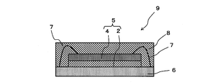
- FIG. 7 is a schematic vertical sectional view showing a preferred embodiment of a semiconductor package manufactured by the method for manufacturing a semiconductor package of the present invention.
- the dicing die-attach film of the present invention is formed by laminating an adhesive layer (dia-attach film) and an adhesive layer (dicing film).
- the dicing die attach film of the present invention may have a form in which an adhesive layer and an adhesive layer are provided in this order on a base material (also referred to as a base film), and a release film is formed on the adhesive layer. It may be provided. It is also preferable that the dicing film and the dicing film have a specific shape as described in the production of the dicing die attach film.
- the adhesive layer of the dicing die attach film of the present invention is a film-like adhesive layer containing an epoxy resin (A), an epoxy resin curing agent (B), a phenoxy resin (C), and an inorganic filler (D). ..
- the phenoxy resin (C) constituting this adhesive layer has an elastic modulus of 500 MPa or more at room temperature (25 ° C.), and is the sum of the contents of the epoxy resin (A) and the phenoxy resin (C) in the adhesive layer.
- the proportion of the phenoxy resin (C) occupying is 10 to 60% by mass.
- the peeling force (peeling force before curing) between the adhesive layer and the pressure-sensitive adhesive layer is 0.40 N / 25 mm or less in the range of 25 to 80 ° C.
- the thermal conductivity of the adhesive layer after thermosetting is 1.0 W / m ⁇ K or more.
- the adhesive layer constituting the dicing die attach film of the present invention contains at least an epoxy resin (A), an epoxy resin curing agent (B), a phenoxy resin (C), and an inorganic filler (D).
- Epoxy resin (A) The epoxy resin (A) can be used without particular limitation as long as it is a thermosetting resin having an epoxy group, and may be liquid, solid or semi-solid.
- a liquid means a softening point of less than 25 ° C.
- a solid means a softening point of 60 ° C. or higher
- a semi-solid means a softening point of the above liquid and a solid. It means that it is between the softening point of (25 ° C or higher and lower than 60 ° C).
- the epoxy resin (A) used in the present invention has a softening point of 100 ° C.
- the softening point is a value measured by a softening point test (ring-ball type) method (measurement conditions: based on JIS-2817).
- the crosslink density of the cured product is increased, and as a result, the contact probability between the blended inorganic fillers (D) is high and the contact area is widened, resulting in higher thermal conductivity.
- the epoxy equivalent is preferably 500 g / eq or less, and more preferably 150 to 450 g / eq.
- the epoxy equivalent means the number of grams (g / eq) of the resin containing 1 equivalent of the epoxy group.
- the mass average molecular weight of the epoxy resin (A) is usually preferably less than 10,000, more preferably 5,000 or less. The lower limit is not particularly limited, but 300 or more is practical.
- the mass average molecular weight is a value obtained by GPC (Gel Permeation Chromatography) analysis.
- the skeleton of the epoxy resin (A) includes phenol novolac type, orthocresol novolac type, cresol novolac type, dicyclopentadiene type, biphenyl type, fluorenbisphenol type, triazine type, naphthol type, naphthalenediol type, triphenylmethane type, Examples thereof include tetraphenyl type, bisphenol A type, bisphenol F type, bisphenol AD type, bisphenol S type, and trimethylolmethane type. Of these, the triphenylmethane type, bisphenol A type, cresol novolac type, and orthocresol novolac type are preferable from the viewpoint of obtaining a film-like adhesive having a low resin crystallinity and a good appearance.
- the content of the epoxy resin (A) in the adhesive layer used in the present invention is preferably 3 to 30% by mass, preferably 5 to 30. More preferably by mass.
- the thermal conductivity of the film-like adhesive can be further improved.
- the value is not more than the above-mentioned preferable upper limit value, it is possible to suppress the formation of the oligomer component and make it difficult for the film state (film tackiness, etc.) to change with a slight temperature change.
- epoxy resin curing agent (B) As the epoxy resin curing agent (B), any curing agent such as amines, acid anhydrides, and polyhydric phenols can be used.
- the adhesive layer containing the epoxy resin (A) and the phenoxy resin (C) described later can have a low melt viscosity in a desired temperature range, and exhibits curability at a high temperature exceeding a certain temperature. It is preferable to use a latent curing agent from the viewpoint of forming an adhesive layer having fast curing property and high storage stability capable of long-term storage at room temperature.
- Potential curing agents include dicyandiamide compounds, imidazole compounds, curing catalyst complex polyvalent phenol compounds, hydrazide compounds, boron trifluoride-amine complexes, amineimide compounds, polyamine salts, and modified products and microcapsules of these. Can be mentioned. It is more preferable to use an imidazole compound from the viewpoint of having more excellent potential (excellent stability at room temperature and exhibiting curability by heating) and a faster curing rate. One of these may be used alone, or two or more thereof may be used in combination.
- the content of the epoxy resin curing agent (B) with respect to 100 parts by mass of the epoxy resin (A) is preferably 0.5 to 100 parts by mass, and more preferably 1 to 80 parts by mass.
- the curing time can be shortened by setting the content to the above-mentioned preferable lower limit value or more, and on the other hand, by setting the content to the above-mentioned preferable upper limit value or less, the residual of excess curing agent in the film-like adhesive can be suppressed. Can be done. As a result, the adsorption of water in the residual curing agent is suppressed, and the reliability of the semiconductor device can be improved.
- the phenoxy resin (C) has an elastic modulus of 500 MPa or more at room temperature (25 ° C.).
- the normal temperature (25 ° C.) elastic modulus of the phenoxy resin (C) is preferably 2000 MPa or less.
- the elastic modulus at room temperature (25 ° C.) (also referred to as “elastic modulus at 25 ° C.” in the present invention) can be determined by the method described in Examples described later.
- the normal temperature (25 ° C.) elastic modulus is determined by using the adhesive layer as a phenoxy resin film for measuring the normal temperature elastic modulus in the method described in Examples described later. It can be determined by using a film prepared by blending a phenoxy resin in a constituent mixing ratio. The normal temperature (25 ° C.) elastic modulus is effective up to the 1st place when the unit is MPa.
- the mass average molecular weight of the phenoxy resin (C) is usually 10,000 or more.
- the upper limit is not particularly limited, but 5,000,000 or less is practical. Of these, 10,000 to 100,000 is more preferable.
- the mass average molecular weight of the phenoxy resin (C) is determined by polystyrene conversion by GPC [Gel Permeation Chromatography].
- the glass transition temperature (Tg) of the phenoxy resin (C) is preferably less than 120 ° C, more preferably less than 100 ° C, and more preferably less than 90 ° C.
- the lower limit is preferably 0 ° C. or higher, more preferably 10 ° C. or higher.
- the glass transition temperature of the phenoxy resin (C) is a glass transition temperature measured by DSC (Differential Scanning Calorimetry) at a heating rate of 0.1 ° C./min.
- the adhesive layer used in the present invention contains at least one type of phenoxy resin as the phenoxy resin (C).
- the epoxy resin (A) and the phenoxy resin (C) are such that the epoxy equivalent (mass of the resin per equivalent epoxy group) is 500 g / eq or less, and the epoxy resin (A) is an epoxy. Resins having an equivalent amount of more than 500 g / eq are classified into phenoxy resins (C).
- the phenoxy resin (C) can be obtained by the reaction of a bisphenol or a biphenol compound with epichlorohydrin such as epichlorohydrin, or the reaction of a liquid epoxy resin with a bisphenol or a biphenol compound.
- the bisphenol or biphenol compound is preferably a compound represented by the following general formula (A).
- L a represents a single bond or a divalent linking group
- R a1 and R a2 are each independently represents a substituent
- ma and na each independently represent an integer of 0-4.
- L a 2 divalent linking group is an alkylene group, a phenylene group, -O -, - S -, - SO -, - SO 2 -, or a group and an alkylene group and a phenylene group are combined is preferable.
- the alkylene group preferably has 1 to 10 carbon atoms, more preferably 1 to 6 carbon atoms, further preferably 1 to 3 carbon atoms, particularly preferably 1 or 2 carbon atoms, and most preferably 1.
- the alkylene group is preferably a group represented by ⁇ C (R ⁇ ) (R ⁇ ) ⁇ .
- R ⁇ and R ⁇ each independently represent a hydrogen atom, an alkyl group, or an aryl group.
- R ⁇ and R ⁇ may combine with each other to form a ring.
- R ⁇ and R ⁇ are preferably hydrogen atoms or alkyl groups (eg, methyl, ethyl, isopropyl, n-propyl, n-butyl, isobutyl, hexyl, octyl, 2-ethylhexyl).
- Alkylene groups among others -CH 2 -, - CH (CH 3) - or -C (CH 3) 2 - are preferred, -CH 2 - or -CH (CH 3) - are more preferable, -CH 2 - Is even more preferable.
- the phenylene group preferably has 6 to 12 carbon atoms, more preferably 6 to 8 carbon atoms, and even more preferably 6.
- Examples of the phenylene group include p-phenylene, m-phenylene and o-phenylene, and p-phenylene or m-phenylene is preferable.
- the alkylene group and the phenylene group in the group in which the alkylene group and the phenylene group are combined the above-mentioned description of the alkylene group and the phenylene group can be preferably applied, respectively.
- an alkylene-phenylene-alkylene group is preferable, and -C (R ⁇ ) (R ⁇ ) -phenylene-C (R ⁇ ) (R ⁇ )-is more preferable.
- the ring formed by combining R ⁇ and R ⁇ is preferably a 5- or 6-membered ring, more preferably a cyclopentane ring or a cyclohexane ring, and even more preferably a cyclohexane ring.
- L a represents a single bond, an alkylene group, -O- or -SO 2 - is preferably an alkylene group is more preferable.
- R a1 and R a2 are preferably an alkyl group, an aryl group, an alkoxy group, an alkylthio group or a halogen atom, more preferably an alkyl group, an aryl group or a halogen atom, and even more preferably an alkyl group.
- na an integer of 0 to 2 is preferable, 0 or 1 is more preferable, and 0 is further preferable.
- the bisphenol or biphenol compound is, for example, bisphenol A, bisphenol AD, bisphenol AP, bisphenol AF, bisphenol B, bisphenol BP, bisphenol C, bisphenol E, bisphenol F, bisphenol G, bisphenol M, bisphenol S, bisphenol P, bisphenol PH, Bisphenol TMC, bisphenol Z, 4,4'-biphenol, 2,2'-dimethyl-4,4'-biphenol, 2,2', 6,6'-tetramethyl-4,4'-biphenol, cardo skeleton
- Examples thereof include bisphenol A, bisphenol AD, bisphenol C, bisphenol E, bisphenol F and 4,4'-biphenol, and preferably bisphenol A, bisphenol E and bisphenol F. More preferably, bisphenol A is particularly preferable.
- the aliphatic diol compound diglycidyl ether is preferable, and the compound represented by the following general formula (B) is more preferable.
- X represents an alkylene group
- nb means an average number of repetitions, and represents 1 to 10.
- the alkylene group preferably has 2 to 10 carbon atoms, more preferably 2 to 8 carbon atoms, further preferably 3 to 8 carbon atoms, particularly preferably 4 to 6 carbon atoms, and most preferably 6 carbon atoms.
- ethylene, propylene, butylene, pentylene, hexylene and octylene can be mentioned, with ethylene, trimethylene, tetramethylene, pentamethylene, heptamethylene, hexamethylene or octamethylene being preferred.
- Nb is preferably 1 to 6, more preferably 1 to 3, and even more preferably 1.
- ethylene is preferably ethylene or propylene, and ethylene is more preferable.
- Examples of the aliphatic diol compound in diglycidyl ether include ethylene glycol, propylene glycol, diethylene glycol, triethylene glycol, polyethylene glycol, 1,3-propanediol, 1,4-butanediol, 1,5-heptandiol, and 1,6. Examples thereof include -hexanediol, 1,7-pentanediol and 1,8-octanediol.
- the bisphenol or biphenol compound or the aliphatic diol compound may be a phenoxy resin obtained by reacting alone or a phenoxy resin obtained by mixing two or more kinds of compounds.
- the reaction of diglycidyl ether of 1,6-hexanediol with a mixture of bisphenol A and bisphenol F can be mentioned.
- the phenoxy resin (C) is preferably a phenoxy resin obtained by reacting a liquid epoxy resin with a bisphenol or a biphenol compound, and more preferably a repeating unit phenoxy resin represented by the following general formula (I).
- L a, R a1, R a2, ma and na are L a, the same meaning as R a1, R a2 ma and na in general formula (A), the preferred range is also the same.
- X and nb are synonymous with X and nb in the general formula (B), and the preferred range is also the same.
- a polymer of bisphenol A and diglycidyl ether of 1,6-hexanediol is preferable.
- the amount of epoxy groups slightly remaining in the phenoxy resin (C) is preferably more than 5000 g / eq in terms of epoxy equivalent.
- the phenoxy resin (C) may be synthesized by the above-mentioned method, or a commercially available product may be used.
- Commercially available products include, for example, 1256 (bisphenol A type phenoxy resin, manufactured by Mitsubishi Chemical Corporation), YP-50 (bisphenol A type phenoxy resin, manufactured by Shin Nikka Epoxy Manufacturing Co., Ltd.), YP-70 (bisphenol A).
- F type phenoxy resin manufactured by Shin Nikka Epoxy Mfg. Co., Ltd.
- FX-316 bisphenol F type phenoxy resin, manufactured by Shin Nikka Epoxy Mfg. Co., Ltd.
- FX-280S cardo skeleton type phenoxy resin, Shinnichi Examples thereof include Chemical Epoxy Mfg.
- the ratio of the phenoxy resin (C) to the total content of the epoxy resin (A) and the phenoxy resin (C) in the adhesive layer is 10 to 60% by mass, preferably 15 to 50% by mass. , 18 to 45% by mass is also more preferable.
- the inorganic filler (D) is not particularly limited as long as it is an inorganic filler having thermal conductivity.
- the inorganic filler (D) imparts thermal conductivity to the adhesive layer.
- the inorganic filler (D) is a particle made of a heat conductive material or a particle whose surface is coated with a heat conductive material, and the heat conductivity of these heat conductive materials is 12 W / m ⁇ K or more. It is preferably 30 W / m ⁇ K or more, and more preferably 30 W / m ⁇ K or more.
- the thermal conductivity of the thermally conductive material is at least the above preferable lower limit value
- the amount of the inorganic filler (D) blended to obtain the desired thermal conductivity can be reduced, and the adhesive layer is melted.
- the increase in viscosity is suppressed, and when crimping to the substrate, the embedding property in the uneven portion of the substrate can be further improved. As a result, the generation of voids can be suppressed more reliably.
- the thermal conductivity of the above-mentioned thermally conductive material means the thermal conductivity at 25 ° C.
- the literature value of each material can be used. Even when not described in the literature, for example, the value measured by JIS R 1611 can be substituted for ceramics, and the value measured by JIS H 7801 can be substituted for metal.
- Examples of the inorganic filler (D) include thermally conductive ceramics, which include alumina particles (thermal conductivity: 36 W / m ⁇ K) and aluminum nitride particles (thermal conductivity: 150 to 290 W / m ⁇ K).
- Boron nitride particles (thermal conductivity: 60 W / m ⁇ K), zinc oxide particles (thermal conductivity: 54 W / m ⁇ K), silicon nitride filler (thermal conductivity: 27 W / m ⁇ K), silicon carbide particles (heat conductivity: 27 W / m ⁇ K) Thermal conductivity: 200 W / m ⁇ K) and magnesium oxide particles (thermal conductivity: 59 W / m ⁇ K) are preferably mentioned.
- alumina particles have high thermal conductivity and are preferable in terms of dispersibility and availability.
- nitride particles and boron nitride particles are preferable from the viewpoint of having a higher thermal conductivity than the alumina particles.
- alumina particles and aluminum nitride particles are particularly preferable.
- particles whose surface is coated with a metal having thermal conductivity can also be mentioned.
- silicone surface-coated with metals such as silver (thermal conductivity: 429 W / m ⁇ K), nickel (thermal conductivity: 91 W / m ⁇ K) and gold (thermal conductivity: 329 W / m ⁇ K).
- Resin particles, acrylic resin particles and the like are preferably mentioned.
- silicone resin particles whose surface is coated with silver are preferable from the viewpoint of stress relaxation and high heat resistance.
- the inorganic filler (D) may be surface-treated or surface-modified, and examples of the compound used for performing such surface treatment or surface modification include a silane coupling agent, phosphoric acid or phosphoric acid. Examples include compounds and surfactants. Except as described herein, for example, the silane coupling agent, phosphoric acid or the term in the section of heat conductive filler in WO 2018/203527 or the section of aluminum nitride filler in WO 2017/158994. The description of phosphoric acid compounds and surfactants can be applied.
- the inorganic filler (D) As a method of blending the inorganic filler (D) with the resin components such as the epoxy resin (A), the epoxy resin curing agent (B) and the phenoxy resin (C), a powdered inorganic filler and, if necessary, silane A method of directly blending a coupling agent, a phosphoric acid or a phosphoric acid compound or a surfactant (inorganic blend method), or a treatment with a surface treatment agent such as a silane coupling agent, a phosphoric acid or a phosphoric acid compound or a surfactant. A method of blending the obtained inorganic filler as a slurry-like inorganic filler dispersed in an organic solvent can be used.
- the method for treating the inorganic filler (D) with the silane coupling agent is not particularly limited, and is a wet method in which the inorganic filler (D) and the silane coupling agent are mixed in a solvent, and inorganic filling in the gas phase. Examples thereof include a dry method in which the agent (D) and a silane coupling agent are treated, and the above-mentioned inorganic blending method.
- aluminum nitride particles contribute to high thermal conductivity, they are likely to generate ammonium ions by hydrolysis, so that they can be used in combination with a phenol resin having a low moisture absorption rate, or hydrolysis is suppressed by surface modification.
- a method for surface modification of aluminum nitride particles a method of providing an oxide layer of aluminum oxide on the surface layer to improve water resistance and surface treatment with phosphoric acid or a phosphoric acid compound to improve affinity with a resin is particularly preferable. preferable.
- a silane coupling agent is a compound in which at least one hydrolyzable group such as an alkoxy group or an aryloxy group is bonded to a silicon atom, and in addition, an alkyl group, an alkenyl group, or an aryl group may be bonded. good.
- the alkyl group is preferably an alkyl group substituted with an amino group, an alkoxy group, an epoxy group or a (meth) acryloyloxy group, and an amino group (preferably a phenylamino group), an alkoxy group (preferably a glycidyloxy group) or (meth).
- An alkyl group substituted with an acryloyloxy group is more preferred.
- silane coupling agent examples include 2- (3,4-epoxycyclohexyl) ethyltrimethoxysilane, 3-glycidyloxypropyltrimethoxysilane, 3-glycidyloxypropyltriethoxysilane, and 3-glycidyloxypropylmethyldimethoxy.
- Silane 3-glycidyloxypropylmethyldiethoxysilane, dimethyldimethoxysilane, dimethyldiethoxysilane, methyltrimethoxysilane, methyltriethoxysilane, phenyltrimethoxysilane, phenyltriethoxysilane, N-phenyl-3-aminopropyltri Examples thereof include methoxysilane, 3-methacryloyl oxypropylmethyldimethoxysilane, 3-methacryloyl oxypropyltrimethoxysilane, 3-methacryloyl oxypropylmethyldiethoxysilane, and 3-methacryloyl oxypropyltriethoxysilane.
- the silane coupling agent and the surfactant are preferably contained in an amount of 0.1 to 2.0 parts by mass with respect to 100 parts by mass of the inorganic filler (D).
- the semiconductor assembly heating step for example, reflow
- the excess silane coupling agent or the surfactant is suppressed while suppressing the aggregation of the inorganic filler (D). It is possible to suppress peeling at the adhesive interface due to volatilization in the step), suppress the generation of voids, and improve the adhesiveness.
- the shape of the inorganic filler (D) examples include flakes, needles, filaments, spheres, and scales, but spherical particles are preferable from the viewpoint of high filling and fluidity.
- the average particle size (d50) of the inorganic filler (D) is preferably 0.1 to 3.5 ⁇ m.
- the average particle size (d50) is the so-called median diameter, and the particle size when the particle size distribution is measured by a laser diffraction / scattering method and the total particle size is 100% in the cumulative distribution, the particle size is 50% cumulative. Means.
- the adhesive layer used in the present invention is the inorganic filler (D) in the total content of the epoxy resin (A), the epoxy resin curing agent (B), the phenoxy resin (C) and the inorganic filler (D).
- the ratio is 30 to 70% by volume.
- the content ratio of the inorganic filler (D) is at least the above lower limit value, the desired thermal conductivity and melt viscosity can be imparted to the film-like adhesive, and a heat dissipation effect from the semiconductor package can be obtained. It is also possible to suppress poor protrusion of the film-like adhesive.
- the ratio of the inorganic filler (D) to the total content of the components (A) to (D) is preferably 20 to 60% by volume, more preferably 20 to 50% by volume.
- the content (volume%) of the inorganic filler (D) can be calculated from the content mass and specific gravity of each component (A) to (D).
- the adhesive layer used in the present invention is high as long as the effects of the present invention are not impaired, in addition to the epoxy resin (A), the epoxy resin curing agent (B), the phenoxy resin (C) and the inorganic filler (D). It may contain a molecular compound.
- the polymer compound include natural rubber, butyl rubber, isoprene rubber, chloroprene rubber, silicone rubber, ethylene-vinyl acetate copolymer, ethylene- (meth) acrylic acid copolymer, and ethylene- (meth) acrylic acid ester.
- Polymers polybutadiene resins, polycarbonate resins, thermoplastic polyimide resins, polyamide resins such as 6-nylon and 6,6-nylon, (meth) acrylic resins, polyester resins such as polyethylene terephthalates and polybutylene terephthalates, polyamideimide resins, fluorine Examples include resin. These polymer compounds may be used alone or in combination of two or more. Further, the adhesive layer used in the present invention may further contain an ion trap agent (ion scavenger), a curing catalyst, a viscosity modifier, an antioxidant, a flame retardant, a colorant and the like. For example, other additives of WO 2017/158994 can be included.
- ion trap agent ion scavenger
- the total content of the epoxy resin (A), the epoxy resin curing agent (B), the phenoxy resin (C) and the inorganic filler (D) in the adhesive layer used in the present invention is, for example, 60 mass by mass. % Or more, preferably 70% by mass or more, more preferably 80% by mass or more, and 90% by mass or more. Further, the above ratio may be 100% by mass or less than 95% by mass.
- the adhesive layer used in the present invention has a thermal conductivity of 1.0 W / m ⁇ K or more after thermosetting.
- the thermal conductivity is preferably 1.4 W / m ⁇ K or more. If the thermal conductivity is less than the above lower limit, it tends to be difficult for the generated heat to escape to the outside of the package.
- the thermally conductive film-like adhesive of the present invention exhibits such excellent thermal conductivity after heat curing, so that the thermally conductive film-like adhesive of the present invention can be applied to an adherend such as a semiconductor wafer or a wiring substrate.
- the upper limit of the thermal conductivity is not particularly limited, but is usually 30 W / m ⁇ K or less.
- the term "after thermosetting" in the measurement of thermal conductivity means a state in which the adhesive layer has been cured. Specifically, it refers to a state in which the heat of reaction peak is no longer observed when DSC (Differential Scanning Calorimetry) measurement is performed at a heating rate of 10 ° C./min.
- the thermal conductivity of such a heat-cured adhesive layer is defined by a thermal conductivity measuring device (trade name: HC-110, manufactured by Eiko Seiki Co., Ltd.) by a thermal flow metering method (JIS). -A value obtained by measuring the thermal conductivity according to A1412). Specifically, the measurement method described in the examples can be referred to.
- the thermal conductivity is valid up to the first decimal place when the unit is W / m ⁇ K.
- the thermal conductivity is determined by the content of the inorganic filler (D), the type of the inorganic filler (D), the epoxy resin (A), the epoxy resin curing agent (B), the phenoxy resin (C), and the like. It can be adjusted to the above range depending on the type of coexisting compound or resin and the content thereof. This also applies to the following pre-curing elastic modulus and melt viscosity.
- the adhesive layer used in the present invention is used before curing in the range of 25 to 80 ° C. when the temperature of the adhesive layer before thermosetting is raised at a heating rate of 25 ° C. to 5 ° C./min.
- the elastic modulus G' is preferably 10 kPa or more.
- the pre-curing elastic modulus at 25 ° C. is preferably 400 kPa or more, more preferably 450 kPa or more, further preferably 500 kPa or more, and preferably 600 kPa or more.
- the adhesive layer before thermosetting means an adhesive layer that has not been exposed to a temperature condition of 25 ° C. or higher after the adhesive layer is formed. Since the dicing die attach film of the present invention is usually stored under a temperature condition of 10 ° C. or lower, the above-mentioned adhesive layer before heat curing is usually at a temperature of 10 ° C. or lower after forming the adhesive layer. Means the adhesive layer that is stored (stored) in.
- the adhesive layer used in the present invention has a melt viscosity at 120 ° C. of 500 to 500 when the temperature of the adhesive layer before thermosetting is raised from 25 ° C. to 5 ° C./min. It is preferably in the range of 10000 Pa ⁇ s, more preferably in the range of 1000 to 10000 Pa ⁇ s, and even more preferably in the range of 1500 to 9200 Pa ⁇ s.
- the melt viscosity can be determined by the method described in Examples described later. The melt viscosity is valid up to the tens place when the unit is Pa ⁇ s.
- a composition (varnish) for forming an adhesive layer containing the constituent components of the adhesive layer is prepared, and this composition is applied onto a release film that has been released and dried. Can be formed.
- the composition for forming an adhesive layer usually contains a solvent.
- the thickness of the adhesive layer is preferably 200 ⁇ m or less, more preferably 100 ⁇ m or less, further preferably 50 ⁇ m or less, preferably 30 ⁇ m or less, and preferably 20 ⁇ m or less.
- the thickness of the adhesive layer is usually 1 ⁇ m or more, preferably 2 ⁇ m or more, and may be 4 ⁇ m or more.
- the thickness of the film-like adhesive can be measured by a contact / linear gauge method (desktop contact type thickness measuring device).
- the release-treated release film may be any as long as it functions as a cover film for the obtained film-like adhesive, and known ones can be appropriately adopted.
- release-treated polypropylene (PP), release-treated polyethylene (PE), and release-treated polyethylene terephthalate (PET) can be mentioned.
- PP polypropylene
- PET release-treated polyethylene
- the coating method a known method can be appropriately adopted, and examples thereof include a method using a roll knife coater, a gravure coater, a die coater, a reverse coater, and the like.
- the arithmetic average roughness Ra of the surface to be bonded to the wafer is preferably 3.0 ⁇ m or less, and the arithmetic average roughness Ra of the surface to be bonded to the adherend is 3.0 ⁇ m or less. More preferably.
- the arithmetic mean roughness Ra is more preferably 2.0 ⁇ m or less, and further preferably 1.5 ⁇ m or less.
- the lower limit is not particularly limited, but it is practically 0.1 ⁇ m or more.
- ⁇ Adhesive layer> As the pressure-sensitive adhesive layer constituting the dicing die attach film of the present invention and the method for forming the same, a general structure and method used as a dicing film (dicing tape) can be appropriately applied.
- a general pressure-sensitive adhesive used for pressure-sensitive adhesive films for example, an acrylic pressure-sensitive adhesive, a rubber-based pressure-sensitive adhesive, or the like can be appropriately used.
- the pressure-sensitive adhesive layer is preferably energy ray-curable.
- acrylic pressure-sensitive adhesive examples include resins composed of (meth) acrylic acid and its esters, unsaturated monomers copolymerizable with (meth) acrylic acid and its esters (eg, vinyl acetate, styrene, etc.). A copolymer or the like with acrylic nitrile or the like is used. Further, two or more kinds of these resins may be mixed and used. Among these, one or more selected from methyl (meth) acrylate, ethylhexyl (meth) acrylate and butyl (meth) acrylate, and hydroxyethyl (meth) acrylate and vinyl acetate are selected as constituents 1 Copolymers containing more than seeds are preferred. This facilitates control of adhesion and adhesiveness with the adherend.
- resins composed of (meth) acrylic acid and its esters, unsaturated monomers copolymerizable with (meth) acrylic acid and its esters (eg, vinyl acetate, styrene,
- a polymerizable group for example, a carbon-carbon unsaturated bond
- Monomers can be blended.
- This polymerizable monomer preferably has two or more (preferably three or more) polymerizable groups. That is, the energy ray curable means having a property of being cured by irradiation with energy rays. Examples of the energy ray include ultraviolet rays and electron beams.
- the descriptions of JP-A-2010-232422, JP-A-2661950, JP-A-2002-226996, JP-A-2005-303275 and the like can be referred to.
- the thickness of the pressure-sensitive adhesive layer is preferably 1 to 200 ⁇ m, more preferably 2 to 100 ⁇ m, further preferably 3 to 50 ⁇ m, and preferably 5 to 30 ⁇ m.
- the dicing die attach film of the present invention has a peeling force of 0.40 N / 25 mm or less in the range of 25 to 80 ° C. between the adhesive layer and the adhesive layer.
- This peeling force is the peeling force between the adhesive layer and the pressure-sensitive adhesive layer after irradiation with energy rays when the pressure-sensitive adhesive layer is energy ray-curable.
- the peeling force between the adhesive layer and the pressure-sensitive adhesive layer at 25 ° C. is preferably 0.30 N / 25 mm or less, more preferably 0.20 N / 25 mm or less.
- the peeling force between the adhesive layer and the pressure-sensitive adhesive layer at 80 ° C. is preferably 0.35 N / 25 mm or less.
- the peeling force can be determined by the method described in Examples. The peeling force is effective up to the second decimal place when the unit is N / 25 mm.
- the method for producing the dicing die attach film of the present invention is not particularly limited as long as it has a structure in which an adhesive layer and an adhesive layer are laminated.
- a coating liquid containing an adhesive is applied on a release liner that has been subjected to a mold release treatment, and dried to form an adhesive layer.
- a film (dicing film) in which an agent layer and a release liner are laminated in this order is produced.
- a composition for forming an adhesive layer is applied on a release film and dried to form an adhesive layer on the release film to prepare a die attach film.
- the dicing film and the die attach film are bonded to each other so that the adhesive layer exposed by peeling the release liner is in contact with the base film, the adhesive layer, the adhesive layer, and the release film. It is possible to obtain a dicing die attach film in which the two are laminated in order.
- the bonding of the dicing film and the die attach film is preferably performed under pressurized conditions.
- the shape of the dicing film is not particularly limited as long as it can cover the opening of the ring frame, but it is preferably circular, and the shape of the dicing film is preferably circular.
- the back surface of the wafer is not particularly limited as long as it can be covered, but it is preferably circular.
- the dicing film is larger than the die attach film, and preferably has a shape having a portion where the adhesive layer is exposed around the adhesive layer. In this way, it is preferable to bond the dicing film and the die attach film cut into a desired shape.
- the dicing die attach film produced as described above is used by peeling off the release film at the time of use.
- FIG. 1 to 7 are schematic vertical sectional views showing a preferred embodiment of each step of the method for manufacturing a semiconductor package of the present invention.
- the back surface of the semiconductor wafer 1 in which at least one semiconductor circuit is formed on the front surface that is, the semiconductor of the semiconductor wafer 1).
- the dicing die attach film of the present invention is thermocompression-bonded to the surface on which the circuit is not formed) on the side of the adhesive layer (that is, the adhesive layer is thermocompression-bonded so as to be in contact with the back surface of the semiconductor wafer), and the semiconductor wafer 1
- the adhesive layer 2 and the adhesive layer 3 are provided in this order.
- the adhesive layer 2 is shown to be smaller than the adhesive layer 3, but the size (area) of both layers is appropriately set according to the purpose.
- the conditions for thermosetting are performed at a temperature at which the epoxy resin (A) is not substantially thermoset.
- the conditions of 70 ° C. and a pressure of 0.3 MPa can be mentioned.
- the semiconductor wafer 1 a semiconductor wafer having at least one semiconductor circuit formed on its surface can be appropriately used, and examples thereof include a silicon wafer, a SiC wafer, a GaAs wafer, and a GaN wafer.
- a known device such as a roll laminator or a manual laminator can be appropriately used.
- the semiconductor chip 4 and the adhesive layer 2 are provided on the pressure-sensitive adhesive layer 3.
- a semiconductor chip 5 with an agent layer is obtained.
- the dicing tape (not shown) is not particularly limited, and a known dicing tape can be used as appropriate.
- the device used for dicing (not shown) is not particularly limited, and a known dicing device can be used as appropriate.
- the adhesive layer is cured with energy rays to reduce the adhesive force, and the adhesive layer 3 is removed from the adhesive layer 2 by a pickup or the like, and then as shown in FIG. ,
- the semiconductor chip 5 with an adhesive layer and the wiring substrate 6 are heat-bonded via the adhesive layer 2, and the semiconductor chip 5 with an adhesive layer is mounted on the wiring substrate 6.
- a substrate having a semiconductor circuit formed on its surface can be appropriately used.
- a printed circuit board (PCB), various lead frames, and electronic components such as resistance elements and capacitors are mounted on the substrate surface.
- the substrate is mentioned.
- the method of mounting the semiconductor chip 5 with an adhesive layer on such a wiring board 6 is not particularly limited, and the semiconductor chip 5 with an adhesive layer is mounted on the wiring board 6 or the surface of the wiring board 6 by using the adhesive layer 2.
- a conventional method capable of adhering to the electronic component mounted on the top can be appropriately adopted.
- the adhesive layer 2 is thermoset.
- the thermosetting temperature is not particularly limited as long as it is equal to or higher than the thermosetting start temperature of the adhesive layer 2, and varies depending on the types of epoxy resin (A), phenoxy resin (C), and epoxy curing agent (B) used. Although it cannot be said unconditionally, for example, 100 to 180 ° C. is preferable, and 140 to 180 ° C. is more preferable from the viewpoint that curing at a higher temperature can be cured in a short time. If the temperature is lower than the thermosetting start temperature, the thermosetting does not proceed and the strength of the adhesive layer 2 tends to decrease.
- the curing treatment time is preferably, for example, 10 to 120 minutes.
- connection method is not particularly limited, and a conventionally known method, for example, a wire bonding method, a TAB (Tape Automated Bonding) method, or the like can be appropriately adopted.
- a plurality of other semiconductor chips 4 can be laminated by thermocompression bonding, thermocompression bonding, and reconnecting to the wiring board 6 by a wire bonding method on the surface of the mounted semiconductor chip 4.
- a method of staggering and laminating semiconductor chips as shown in FIG. 5, or a method of laminating while embedding a bonding wire 7 by thickening the second and subsequent adhesive layers 2 as shown in FIG. be.
- the sealing resin 8 is not particularly limited, and an appropriately known sealing resin that can be used for manufacturing a semiconductor package can be used. Further, the sealing method using the sealing resin 8 is not particularly limited, and a known method can be appropriately adopted.
- the semiconductor package of the present invention is formed by bonding a semiconductor chip and a wiring substrate or a semiconductor chip with a heat-cured material of an adhesive layer of the dicing die attach film of the present invention.
- the semiconductor package of the present invention as shown in FIGS. 4 and 7, the semiconductor chip 4 and the wiring board 6 are bonded to each other by the thermosetting body of the adhesive layer of the dicing die attach film of the present invention.
- An example is a semiconductor package 9 having a structure (in FIG. 7, a semiconductor package 9 in which the structure is sealed). Further, as another example of the semiconductor package of the present invention, as shown in FIGS.
- the dicing die attach film of the present invention is formed between the semiconductor chips 4.
- Examples thereof include a semiconductor package 9 having a structure in which the adhesive layer of the semiconductor is bonded by a heat-cured material.
- the adhesive layer in the dicing die attach film of the present invention for bonding between the semiconductor chips when the semiconductor chips are laminated in multiple stages, the heat of the adhesive layer possessed by the dicing die attach film of the present invention is generated between the semiconductor chips.
- a semiconductor package having a structure bonded by a cured product can be obtained.
- the semiconductor chip and the wiring substrate may be adhered by the heat-cured material of the adhesive layer of the dicing die attach film of the present invention (for example, FIGS. 5 and 6), and the adhesive is thermally conductive. It may be adhered by an adhesive layer usually used as an agent layer. However, it is preferable that the dicing die attach film of the present invention is adhered by the thermosetting body of the adhesive layer 2.
- the adhesive layer 2 described between the semiconductor chip 4 and the wiring substrate 6 and between the semiconductor chips 4 is in a thermosetting state. That is, it exists in a state where each member is adhered as a thermosetting body of an adhesive layer.
- room temperature means 25 ° C.
- MEK is methyl ethyl ketone
- PET is polyethylene terephthalate.
- Example 1 [1. Preparation of adhesive layer (dicing film)] (1) Preparation of base film Resin pellets of low-density polyethylene (LDPE, density 0.92 g / cm 3 , melting point 110 ° C) are melted at 230 ° C and made into a long film with a thickness of 70 ⁇ m using an extruder. Molded. The obtained film was irradiated with an electron beam of 100 kGy to prepare a base film.
- LDPE low-density polyethylene
- Coronate L (trade name, manufactured by Nippon Polyurethane Industry Co., Ltd.) was added as a polyisocyanate to 100 parts by mass of the acrylic copolymer prepared above, and Ethyl KIP 150 (trade name, trade name, manufactured by Nippon Polyurethane Industry Co., Ltd.) was added as a photopolymerization initiator.
- this pressure-sensitive adhesive composition was applied onto a release liner made of a release-treated polyethylene terephthalate (PET) film so as to have a thickness of 20 ⁇ m after drying, and dried at 110 ° C. for 3 minutes for adhesion.
- PET polyethylene terephthalate
- the base film prepared above and the pressure-sensitive adhesive layer were laminated to prepare a dicing film in which the pressure-sensitive adhesive layer was formed on the base film.
- Triphenylmethane type epoxy resin (trade name: EPPN-501H, mass average molecular weight: 1000, softening point: 55 ° C., semi-solid, epoxy equivalent: 167 g / eq, manufactured by Nippon Kayaku Co., Ltd.) 56 parts by mass, bisphenol A Type Epoxy resin (trade name: YD-128, mass average molecular weight: 400, softening point: less than 25 ° C, liquid, epoxy equivalent: 190 g / eq, manufactured by Shin Nikka Epoxy Manufacturing Co., Ltd.) 49 parts by mass, bisphenol A type Phenoxy resin (trade name: YP-50, mass average molecular weight: 70000, Tg: 84 ° C., normal temperature (25 ° C.) elasticity: 1700 MPa, manufactured by Shin-Nippon Epoxy Manufacturing Co., Ltd.) 30 parts by mass and 67 parts by mass of MEK 1000 ml A resin varnish was obtained by
- the obtained mixed varnish was applied onto a release-treated PET film (release film) having a thickness of 38 ⁇ m, dried by heating at 130 ° C. for 10 minutes, and an adhesive layer having a length of 300 mm, a width of 200 mm, and a thickness of 10 ⁇ m was applied.
- a release-treated PET film release film having a thickness of 38 ⁇ m
- an adhesive layer having a length of 300 mm, a width of 200 mm, and a thickness of 10 ⁇ m was applied.
- the thickness is a value measured by the above method.
- the dicing film was cut into a circular shape so that the dicing film could be attached so as to cover the opening of the ring frame. Further, the die attach film was cut into a circular shape so as to cover the back surface of the wafer.
- the adhesive layer exposed by peeling the release liner from the dicing film cut as described above and the adhesive layer of the die attach film cut as described above are loaded with a load of 0.4 MPa using a roll press machine.
- a dicing die attach film was prepared by laminating under the condition of a speed of 1.0 m / min. This dicing die attach film has a portion in which the dicing film is larger than the die attach film and the adhesive layer is exposed around the adhesive layer.
- Example 2 A dicing die attach film was produced in the same manner as in Example 1 except that 320 parts by mass of an alumina filler (trade name: AO-502, manufactured by Admatex Co., Ltd., average particle size (d50): 0.6 ⁇ m) was used. ..
- Example 3 A dicing die attach film was produced in the same manner as in Example 1 except that 480 parts by mass of an alumina filler (trade name: AO-502, manufactured by Admatex Co., Ltd., average particle size (d50): 0.6 ⁇ m) was used. ..
- Example 4 Bisphenol A / F copolymerized phenoxy resin instead of bisphenol A type phenoxy resin (trade name: YP-70, mass average molecular weight: 55000, Tg: 72 ° C., normal temperature (25 ° C.) elasticity: 1400 MPa, Nikka epoxy A dicing die attach film was produced in the same manner as in Example 1 except that 30 parts by mass (manufactured by Manufacture Co., Ltd.) was used.
- Example 5 Low elasticity and high heat resistance type phenoxy resin instead of bisphenol A type phenoxy resin (trade name: FX-310, mass average molecular weight: 40,000, Tg: 110 ° C. A dicing die attach film was produced in the same manner as in Example 1 except that 30 parts by mass was used.
- Example 6 Bisphenol A type phenoxy resin (trade name: YP-50, mass average molecular weight: 70000, Tg: 84 ° C, normal temperature (25 ° C) elastic modulus: 1700 MPa, manufactured by Shin Nikka Epoxy Manufacturing Co., Ltd.) 44 parts by mass, alumina filler A dicing die attach film was produced in the same manner as in Example 1 except that 350 parts by mass (trade name: AO-502, manufactured by Admatex Co., Ltd., average particle size (d50): 0.6 ⁇ m) was used.
- AO-502 manufactured by Admatex Co., Ltd., average particle size (d50): 0.6 ⁇ m
- Example 7 Bisphenol A type phenoxy resin (trade name: YP-50, mass average molecular weight: 70000, Tg: 84 ° C, normal temperature (25 ° C) elastic modulus: 1700 MPa, manufactured by Shin Nikka Epoxy Manufacturing Co., Ltd.) 70 parts by mass, alumina filler A dicing die attach film was produced in the same manner as in Example 1 except that 400 parts by mass (trade name: AO-502, manufactured by Admatex Co., Ltd., average particle size (d50): 0.6 ⁇ m) was used.
- AO-502 manufactured by Admatex Co., Ltd.
- Example 8 Bisphenol A type phenoxy resin (trade name: YP-50, mass average molecular weight: 70000, Tg: 84 ° C, normal temperature (25 ° C) elastic modulus: 1700 MPa, manufactured by Shin Nikka Epoxy Manufacturing Co., Ltd.) 50 parts by mass, silver filler (Product name: AG-4-8F, manufactured by DOWA Electronics Co., Ltd., average particle size (d50): 2.0 ⁇ m)
- a dicing die attach film was produced in the same manner as in Example 1 except that 360 parts by mass was used. ..
- Example 9 Bisphenol A type phenoxy resin (trade name: YP-50, mass average molecular weight: 70000, Tg: 84 ° C, normal temperature (25 ° C) elastic modulus: 1700 MPa, manufactured by Shin Nikka Epoxy Manufacturing Co., Ltd.) 50 parts by mass, silver filler (Product name: AG-4-8F, manufactured by DOWA Electronics Co., Ltd., average particle size (d50): 2.0 ⁇ m)
- a dicing die attach film was produced in the same manner as in Example 1 except that 610 parts by mass was used. ..
- Example 10 Bisphenol A type phenoxy resin (trade name: YP-50, mass average molecular weight: 70000, Tg: 84 ° C, normal temperature (25 ° C) elastic modulus: 1700 MPa, manufactured by Shin Nikka Epoxy Manufacturing Co., Ltd.) 50 parts by mass, silver filler A dicing die attach film was produced in the same manner as in Example 1 except that 950 parts by mass was used (trade name: AG-4-8F, manufactured by DOWA Electronics Co., Ltd., average particle size (d50): 2.0 ⁇ m). ..
- Acrylic polymer solution (trade name: S-2060, mass average molecular weight: 500000, Tg: -23 ° C, normal temperature (25 ° C) elastic modulus: 50 MPa, solid content 25% (organic solvent: toluene), manufactured by Toa Synthetic Co., Ltd. ) 120 parts by mass (of which the amount of the acrylic polymer itself is 30 parts by mass), alumina filler (trade name: AO-502, manufactured by Admatex Co., Ltd., average particle size (d50): 0.6 ⁇ m) 320 parts by mass.
- a dicing die attach film was produced in the same manner as in Example 1 except that it was used.
- a square with a size of 5.0 cm in length ⁇ 5.0 cm in width is cut out from the dicing die attach film prepared above, the dicing film (adhesive layer and base film) and the release film are peeled off, and the cut samples are laminated.
- a test piece of an adhesive layer having a thickness of about 1.0 mm was obtained by bonding with a hand roller on a hot plate at a stage of 70 ° C.
- a rheometer (RS6000, manufactured by Hake) was used to measure the change in viscous resistance in a temperature range of 20 to 250 ° C. and a heating rate of 5 ° C./min.
- the dicing die attach film produced above is irradiated with ultraviolet rays from the dicing film (adhesive layer) side using an ultraviolet irradiation device (trade name: RAD-2000F / 8, manufactured by Lintec Co., Ltd., irradiation amount 200 mJ / cm 2 ). Then, the delamination strength between the adhesive layer and the dicing film (adhesive layer and base film) was measured in a constant temperature bath at room temperature and 80 ° C., respectively. Measurement conditions: JISZ0237 compliant, 180 ° peel test Measuring device: Tensile tester (manufactured by Shimadzu Corporation, model number: TCR1L type)
- the release film of the dicing die attach film produced above is peeled off, and a dummy silicon wafer (8 inch) is used at a temperature of 70 ° C. and a pressure of 0.3 MPa using a manual laminator (trade name: FM-114, manufactured by Technovision Co., Ltd.). It was adhered to one surface (size, thickness 100 ⁇ m).
- a dicing device (trade name: DFD-6340, manufactured by DISCO) equipped with a two-axis dicing blade (Z1: NBC-ZH2050 (27HEDD), manufactured by DISCO / Z2: NBC-ZH127F-SE (BC), manufactured by DISCO).
- Dicing was performed from the dummy silicon wafer side so as to have a square size of 10 mm ⁇ 10 mm using DISCO Corporation) to obtain a dummy chip with an adhesive layer.
- ultraviolet irradiation was performed from the back surface side of the wafer using an ultraviolet irradiation device (trade name: RAD-2000F / 8, manufactured by Lintec Corporation, irradiation amount 200 mJ / cm 2 ), and a die bonder (trade name: DB-800, Co., Ltd.) was used.
- thermosetting A square piece having a side of 50 mm or more is cut out from the dicing die attach film produced above, the dicing film (adhesive layer and base film) and the release film are peeled off, and the cut samples are overlapped and adhered to a thickness of 5 mm or more.
- An agent layer laminate was obtained. This sample is placed on a disk-shaped die having a diameter of 50 mm and a thickness of 5 mm, heated using a compression press molding machine at a temperature of 150 ° C. and a pressure of 2 MPa for 10 minutes, and then taken out, and then further heated at a temperature of 180 in a dryer.
- the adhesive layer was thermoset by heating at ° C.
- a thermal conductivity measuring device (trade name: HC-110, manufactured by Eiko Seiki Co., Ltd.) was used, and the thermal conductivity (W / (m ⁇ K) was measured by the heat flow metering method (based on JIS-A1412). )) was measured.
- the release film of the dicing die attach film produced above is peeled off, and a dummy silicon wafer (8 inch) is used at a temperature of 70 ° C. and a pressure of 0.3 MPa using a manual laminator (trade name: FM-114, manufactured by Technovision Co., Ltd.). It was adhered to one surface (size, thickness 100 ⁇ m).
- a dicing device (trade name: DFD-6340, manufactured by DISCO) equipped with a two-axis dicing blade (Z1: NBC-ZH2050 (27HEDD), manufactured by DISCO / Z2: NBC-ZH127F-SE (BC), manufactured by DISCO).
- Dicing was performed from the dummy silicon wafer side so as to have a square size of 5 mm ⁇ 5 mm using DISCO Corporation) to obtain a dummy chip with an adhesive layer.
- ultraviolet rays were irradiated from the back surface side of the wafer using an ultraviolet irradiation device (trade name: RAD-2000F / 8, manufactured by Lintec Corporation, irradiation amount 200 mJ / cm 2 ), and a die bonder (trade name: DB-800, Co., Ltd.) was used.
- the average particle size (d50) was obtained from the cumulative curve of the volume fraction of the particle size distribution measured by the laser diffraction / scattering method (model: LMS-2000e, manufactured by Seishin Co., Ltd.). rice field.
- this resin varnish is applied onto a release-treated PET film (release film) having a thickness of 38 ⁇ m, dried by heating at 130 ° C. for 10 minutes, and has a length of 300 mm, a width of 200 mm, and a thickness of 100 ⁇ m.
- a dynamic viscoelasticity measuring device (trade name: Rheogel-E4000F, manufactured by UBM Co., Ltd.) is used to measure a temperature range of 0 to 100 ° C. and a heating rate of 5 The measurement was carried out under the conditions of ° C./min and a frequency of 1 Hz, and the value of the elastic modulus at 25 ° C. was determined.
- the acrylic resin used in Comparative Example 5 the elastic modulus at 25 ° C. was determined according to the above method in the same manner as the phenoxy resin.
- Tg Glass transition temperature of phenoxy resin
- the phenoxy resin film produced by the method described in the above measurement of elastic modulus was measured using a differential scanning calorimeter (model number: DSC7000, manufactured by Hitachi High-Tech Science Co., Ltd.) under the condition of a temperature rise rate of 5 ° C./min.
- the temperature at which the baseline shifts to the heat absorption peak side was measured as the glass transition temperature (Tg).
- the elastic modulus, the glass transition temperature, and the mass average molecular weight at 25 ° C. were determined according to the above method in the same manner as the phenoxy resin.
- a "-" in the column of adhesive layer means that the component is not contained.
- the ratio of the phenoxy resin (C) to the total content of the epoxy resin (A) and the phenoxy resin (C) is less than 10% by mass, and the adhesive at 80 ° C.
- the peeling force between the layer and the pressure-sensitive adhesive layer exceeds 0.40 N / 25 mm.
- the dicing die attach film of Comparative Example 1 is inferior in pickability because, when continuously picked up due to the heat storage of the pickup collet, 11 or more chips out of 96 chips have a pickup failure. rice field.
- the ratio of the phenoxy resin (C) to the total content of the epoxy resin (A) and the phenoxy resin (C) exceeds 60% by mass.
- the dicing die attach films of Comparative Examples 2 and 3 when heat-bonded to the wiring board, voids were generated in 6 or more of the 24 chips, and the suppression of void generation was insufficient. rice field.
- the dicing die attach film of Comparative Example 3 has a low thermal conductivity of less than 1.0 W / m ⁇ K of the adhesive layer after thermosetting, and has sufficient heat dissipation as an adhesive applied to a semiconductor package. There wasn't.
- the elastic modulus of the phenoxy resin (C) at 25 ° C. is less than 500 MPa.
- the dicing die attach film of Comparative Example 5 does not contain a phenoxy resin, but contains an acrylic resin (elastic modulus at 25 ° C. is less than 500 MPa).
- the dicing die attach films of Examples 1 to 10 of the present invention were excellent in continuous pick-up property in semiconductor processing, and even if the pickup collet stored heat, pickup failure was unlikely to occur. In addition, it was also excellent in suppressing the generation of voids when heat-bonding to the wiring board.
Landscapes
- Chemical & Material Sciences (AREA)
- Organic Chemistry (AREA)
- Chemical Kinetics & Catalysis (AREA)
- Health & Medical Sciences (AREA)
- Medicinal Chemistry (AREA)
- Polymers & Plastics (AREA)
- Inorganic Chemistry (AREA)
- Adhesives Or Adhesive Processes (AREA)
- Die Bonding (AREA)
- Dicing (AREA)
- Adhesive Tapes (AREA)
- Engineering & Computer Science (AREA)
- Manufacturing & Machinery (AREA)
Abstract
接着剤層と粘着剤層とが積層されてなるダイシングダイアタッチフィルムであって、 前記接着剤層が、エポキシ樹脂(A)、エポキシ樹脂硬化剤(B)、フェノキシ樹脂(C)及び無機充填材(D)を含有するフィルム状接着剤の層であり、 前記フェノキシ樹脂(C)の25℃における弾性率が500MPa以上であり、 前記接着剤層中、前記エポキシ樹脂(A)と前記フェノキシ樹脂(C)の各含有量の合計に占める前記フェノキシ樹脂(C)の割合が、10~60質量%であり、 前記接着剤層と前記粘着剤層の25~80℃の範囲における剥離力が0.40N/25mm以下であり、 前記接着剤層は、熱硬化後の熱伝導率が1.0W/m・K以上であることを特徴とする、ダイシングダイアタッチフィルム。
Description
本発明は、ダイシングダイアタッチフィルム、並びに、ダイシングダイアタッチフィルムを用いた半導体パッケージ及びその製造方法に関する。
近年、電子機器の小型化及び高機能化、多機能化が進む中で、その内部に搭載される半導体パッケージにおいても高機能化、多機能化が進んでおり、半導体ウェハ配線ルールの微細化が進行している。高機能化、多機能化に伴い、半導体チップを多段に積層したスタックドMCP(Multi Chip Package)が普及しており、携帯電話、携帯オーディオ機器用のメモリパッケージなどに搭載されている。また、携帯電話等の多機能化に伴い、パッケージの高密度化、高集積化も推し進められている。これに伴い、半導体チップの多段積層化がさらに進行している。
このようなメモリパッケージの製造過程における配線基板と半導体チップとの接着、また、半導体チップ間の接着(いわゆる、ダイアタッチ)には、フィルム状接着剤(ダイアタッチフィルム)が使用され、チップの多段積層化に伴い、ダイアタッチフィルムの薄膜化も要求されている。また、近年、ウェハ配線ルールの微細化が進行しており、半導体素子表面には熱がより一層発生しやすい。したがって、熱をパッケージ外部へ逃がし易くするために、これらダイアタッチフィルムには高熱伝導性の要求が高まってきている。
熱伝導性ダイアタッチフィルムとしては、一般的に熱伝導性フィラーを用いたフィルムが設計されている。
熱伝導性ダイアタッチフィルムとしては、一般的に熱伝導性フィラーを用いたフィルムが設計されている。
熱伝導性ダイアタッチフィルムとして用いることができる材料としては、例えば、特許文献1に、平均粒径2~9μmで比表面積が0.8~8.0m2/gである球状アルミナフィラーと、特定の重量含有比率で高分子量成分及び低分子量成分を含む樹脂成分とを含む、ダイボンディングフィルムとして使用される接着シートが記載されている。特許文献1記載の技術によれば、この接着シートを用いることで被着体の凹凸部への埋め込み性が高まり、ボイドの発生を抑制できるとされる。
また、特許文献2には、ダイアタッチ層と粘着層と基材層とがこの順に積層されたダイシングダイアタッチフィルムにおいて、ダイアタッチ層と粘着層との常温時と高温時の剥離力を制御することにより、ピックアップ不安定性が改善されることが記載されている。
また、特許文献2には、ダイアタッチ層と粘着層と基材層とがこの順に積層されたダイシングダイアタッチフィルムにおいて、ダイアタッチ層と粘着層との常温時と高温時の剥離力を制御することにより、ピックアップ不安定性が改善されることが記載されている。
本発明者は、熱伝導性接着剤層(熱伝導性ダイアタッチフィルム)と粘着剤層(ダイシングフィルム)とを積層してなるダイシングダイアタッチフィルムを用いた半導体ウェハのダイシング~ピックアップ工程について、半導体装置の生産性の向上を企図して検討を重ねた。その結果、半導体ウェハのダイシングによるチップ化後、ピックアップコレットを用いて、チップ裏面に熱伝導性ダイアタッチフィルムを残してダイシングフィルムから剥離し、このチップを配線基板上に熱圧着する工程を繰り返すうちに、ピックアップコレットが蓄熱すること、蓄熱したピックアップコレットを用いてチップをピックアップすると、熱伝導率の高いダイアタッチフィルムを介してダイシングフィルムにも熱が伝達し、ダイアタッチフィルムとダイシングフィルムとの剥離性が低下してピックアップ不良が生じやすくなることがわかってきた。
本発明は、熱伝導性ダイアタッチフィルムとダイシングフィルムとを積層してなるダイシングダイアタッチフィルムであって、半導体加工におけるピックアップ工程において、ピックアップコレットが蓄熱してもピックアップ不良を生じにくく、また、配線基板に熱圧着した際のボイドの発生も抑制できるダイシングダイアタッチフィルムを提供することを課題とする。
本発明者は上記課題に鑑み鋭意検討を重ねた結果、ダイアタッチフィルムの構成材料にフェノキシ樹脂を含有させることにより、無機充填剤を含む熱伝導性ダイアタッチフィルムとしながらも、ピックアップ工程におけるダイシングフィルムとの剥離性が改善することがわかってきた。さらに、本発明者は、フェノキシ樹脂として常温(25℃)弾性率が一定以上の値を示すものを採用し、エポキシ樹脂及びその硬化剤とを組合せて各特定量配合して、熱硬化後の熱伝導率が一定以上に高まるよう制御したダイアタッチフィルムにより、上記課題を、より高いレベルで解決でき、さらにダイアタッチ性も高められることを見い出した。
本発明はこれらの知見に基づきさらに検討を重ねて完成されるに至ったものである。
本発明はこれらの知見に基づきさらに検討を重ねて完成されるに至ったものである。
本発明の上記課題は下記の手段により解決される。
〔1〕
接着剤層と粘着剤層とが積層されてなるダイシングダイアタッチフィルムであって、
前記接着剤層が、エポキシ樹脂(A)、エポキシ樹脂硬化剤(B)、フェノキシ樹脂(C)及び無機充填材(D)を含有するフィルム状接着剤の層であり、
前記フェノキシ樹脂(C)の25℃における弾性率が500MPa以上であり、
前記接着剤層中、前記エポキシ樹脂(A)と前記フェノキシ樹脂(C)の各含有量の合計に占める前記フェノキシ樹脂(C)の割合が、10~60質量%であり、
前記接着剤層と前記粘着剤層の25~80℃の範囲における剥離力が0.40N/25mm以下であり、
前記接着剤層は、熱硬化後の熱伝導率が1.0W/m・K以上であることを特徴とする、ダイシングダイアタッチフィルム。
〔2〕
前記接着剤層を25℃から5℃/分の昇温速度で昇温したとき、25~80℃の範囲における硬化前弾性率G’が10kPa以上であることを特徴とする、〔1〕に記載のダイシングダイアタッチフィルム。
〔3〕
前記接着剤層を25℃から5℃/分の昇温速度で昇温したとき、120℃における溶融粘度が500~10000Pa・sの範囲にあることを特徴とする、〔1〕又は〔2〕に記載のダイシングダイアタッチフィルム。
〔4〕
前記粘着剤層がエネルギー線硬化性である、〔1〕~〔3〕のいずれか1項に記載のダイシングダイアタッチフィルム。
〔5〕
表面に少なくとも1つの半導体回路が形成された半導体ウェハの裏面に、〔1〕~〔4〕のいずれか1項に記載のダイシングダイアタッチフィルムを、前記接着剤層を半導体ウェハの裏面に接するように熱圧着して設ける第1の工程と、
前記半導体ウェハと前記接着剤層とを同時にダイシングすることにより、粘着剤層上に、前記半導体チップ及び前記接着剤層を備える接着剤層付き半導体チップを得る第2の工程と、
前記接着剤層から前記粘着剤層を取り除き、前記接着剤層付き半導体チップと配線基板とを前記接着剤層を介して熱圧着する第3の工程と、
前記接着剤層を熱硬化する第4の工程と、
を含むことを特徴とする半導体パッケージの製造方法。
〔6〕
半導体チップと配線基板、又は、半導体チップ間が、〔1〕~〔4〕のいずれか1項に記載のダイシングダイアタッチフィルムが有する接着剤層の熱硬化体により接着されてなることを特徴とする、半導体パッケージ。
本発明において「~」を用いて表される数値範囲は、「~」前後に記載される数値を下限値及び上限値として含む範囲を意味する。
本発明において、(メタ)アクリルとは、アクリル及びメタアクリルの一方又は両方を意味する。(メタ)アクリレートについても同様である。
本発明において、各成分は、それぞれ1種を用いてもよく、2種以上を混合して用いてもよい。
本発明において、(メタ)アクリルとは、アクリル及びメタアクリルの一方又は両方を意味する。(メタ)アクリレートについても同様である。
本発明において、各成分は、それぞれ1種を用いてもよく、2種以上を混合して用いてもよい。
本発明のダイシングダイアタッチフィルムは、熱伝導性ダイアタッチフィルムとダイシングフィルムとを積層してなり、半導体加工におけるピックアップ工程において、ピックアップコレットが蓄熱した状態になってもピックアップ不良を生じにくく、また、ダイアタッチ性にも優れる。
[ダイシングダイアタッチフィルム]
本発明のダイシングダイアタッチフィルムは、接着剤層(ダイアタッチフィルム)と粘着剤層(ダイシングフィルム)とが積層されてなる。本発明のダイシングダイアタッチフィルムは、基材(基材フィルムとも称す。)上に粘着剤層と接着剤層とがこの順に設けられた形態とすることができ、接着剤層上に剥離フィルムが設けられていてもよい。また、ダイシングフィルム及びダイアタッチフィルムは、ダイシングダイアタッチフィルムの作製において記載するように、特定の形状であることも好ましい。
本発明のダイシングダイアタッチフィルムの接着剤層は、エポキシ樹脂(A)、エポキシ樹脂硬化剤(B)、フェノキシ樹脂(C)及び無機充填材(D)を含有するフィルム状接着剤の層である。
この接着剤層を構成するフェノキシ樹脂(C)は、常温(25℃)弾性率が500MPa以上であり、接着剤層中、エポキシ樹脂(A)とフェノキシ樹脂(C)の各含有量の合計に占めるフェノキシ樹脂(C)の割合は10~60質量%である。
また、本発明のダイシングダイアタッチフィルムは、接着剤層と粘着剤層との間の剥離力(硬化前剥離力)が、25~80℃の範囲において、0.40N/25mm以下である。また、接着層の熱硬化後の熱伝導率が1.0W/m・K以上である。
本発明のダイシングダイアタッチフィルムを構成する各層の形態について、順に説明する。
<接着剤層>
本発明のダイシングダイアタッチフィルムを構成する接着剤層は、エポキシ樹脂(A)、エポキシ樹脂硬化剤(B)、フェノキシ樹脂(C)及び無機充填材(D)を少なくとも含有する。
本発明のダイシングダイアタッチフィルムを構成する接着剤層は、エポキシ樹脂(A)、エポキシ樹脂硬化剤(B)、フェノキシ樹脂(C)及び無機充填材(D)を少なくとも含有する。
(エポキシ樹脂(A))
上記エポキシ樹脂(A)は、エポキシ基を持つ熱硬化型の樹脂である限り、特に制限なく用いることができ、液体、固体または半固体のいずれであってもよい。本発明において液体とは、軟化点が25℃未満であることをいい、固体とは、軟化点が60℃以上であることをいい、半固体とは、軟化点が上記液体の軟化点と固体の軟化点との間(25℃以上60℃未満)にあることをいう。本発明で使用するエポキシ樹脂(A)としては、好適な温度範囲(例えば60~120℃)で低溶融粘度に到達することができるフィルム状接着剤を得る観点から、軟化点が100℃以下であることが好ましい。なお、本発明において、軟化点とは、軟化点試験(環球式)法(測定条件:JIS-2817に準拠)により測定した値である。
上記エポキシ樹脂(A)は、エポキシ基を持つ熱硬化型の樹脂である限り、特に制限なく用いることができ、液体、固体または半固体のいずれであってもよい。本発明において液体とは、軟化点が25℃未満であることをいい、固体とは、軟化点が60℃以上であることをいい、半固体とは、軟化点が上記液体の軟化点と固体の軟化点との間(25℃以上60℃未満)にあることをいう。本発明で使用するエポキシ樹脂(A)としては、好適な温度範囲(例えば60~120℃)で低溶融粘度に到達することができるフィルム状接着剤を得る観点から、軟化点が100℃以下であることが好ましい。なお、本発明において、軟化点とは、軟化点試験(環球式)法(測定条件:JIS-2817に準拠)により測定した値である。
本発明で使用するエポキシ樹脂(A)において、硬化体の架橋密度が高くなり、結果として、配合される無機充填剤(D)同士の接触確率が高く接触面積が広くなることでより高い熱伝導率が得られる観点から、エポキシ当量は500g/eq以下であることが好ましく、150~450g/eqであることがより好ましい。なお、本発明において、エポキシ当量とは、1当量のエポキシ基を含む樹脂のグラム数(g/eq)をいう。
エポキシ樹脂(A)の質量平均分子量は、通常、10,000未満が好ましく、5,000以下がより好ましい。下限値に特に制限はないが、300以上が実際的である。
質量平均分子量は、GPC(Gel Permeation Chromatography)分析による値である。
エポキシ樹脂(A)の質量平均分子量は、通常、10,000未満が好ましく、5,000以下がより好ましい。下限値に特に制限はないが、300以上が実際的である。
質量平均分子量は、GPC(Gel Permeation Chromatography)分析による値である。
エポキシ樹脂(A)の骨格としては、フェノールノボラック型、オルソクレゾールノボラック型、クレゾールノボラック型、ジシクロペンタジエン型、ビフェニル型、フルオレンビスフェノール型、トリアジン型、ナフトール型、ナフタレンジオール型、トリフェニルメタン型、テトラフェニル型、ビスフェノールA型、ビスフェノールF型、ビスフェノールAD型、ビスフェノールS型、トリメチロールメタン型等が挙げられる。これらのうち、樹脂の結晶性が低く、良好な外観を有するフィルム状接着剤を得られる観点から、トリフェニルメタン型、ビスフェノールA型、クレゾールノボラック型、オルソクレゾールノボラック型が好ましい。
本発明に用いる接着剤層中(接着剤層形成用組成物の固形分(溶媒を除いた全量)中)、エポキシ樹脂(A)の含有量は、3~30質量%が好ましく、5~30質量%がより好ましい。含有量を上記好ましい下限値以上とすることにより、フィルム状接着剤の熱伝導率をより向上させることができる。他方、上記好ましい上限値以下とすることにより、オリゴマー成分の生成を抑え、多少の温度変化ではフィルム状態(フィルムタック性等)の変化を生じにくくすることができる。
(エポキシ樹脂硬化剤(B))
上記エポキシ樹脂硬化剤(B)としては、アミン類、酸無水物類、多価フェノール類等の任意の硬化剤を用いることができる。本発明では、上記エポキシ樹脂(A)および後記フェノキシ樹脂(C)を含む接着剤層を所望の温度範囲で低溶融粘度とすることができ、かつある温度を超える高温で硬化性を発揮し、速硬化性を有し、さらに、室温での長期保存が可能な保存安定性の高い接着剤層とする観点から、潜在性硬化剤を用いることが好ましい。
潜在性硬化剤としては、ジシアンジアミド化合物、イミダゾール化合物、硬化触媒複合系多価フェノール化合物、ヒドラジド化合物、三弗化ホウ素-アミン錯体、アミンイミド化合物、ポリアミン塩、およびこれらの変性物やマイクロカプセル型のものを挙げることができる。より優れた潜在性(室温での安定性に優れ、かつ、加熱により硬化性を発揮する性質)を有し、硬化速度がより速い観点から、イミダゾール化合物を用いることがより好ましい。
これらは1種を単独で用いてもよく、2種以上を組み合わせて用いてもよい。
エポキシ樹脂(A)100質量部に対するエポキシ樹脂硬化剤(B)の含有量は、0.5~100質量部が好ましく、1~80質量部がより好ましい。含有量を上記好ましい下限値以上とすることにより硬化時間をより短くすることができ、他方、上記好ましい上限値以下とすることにより、過剰の硬化剤のフィルム状接着剤中への残留を抑えることができる。結果、残留硬化剤の水分の吸着が抑えられ、半導体装置の信頼性の向上を図ることができる。
(フェノキシ樹脂(C))
上記フェノキシ樹脂(C)は、常温(25℃)弾性率が500MPa以上である。上記フェノキシ樹脂(C)の常温(25℃)弾性率は、2000MPa以下が好ましい。このような弾性率を有するフェノキシ樹脂を用いることにより、ダイアタッチ性とピックアップ性の両立をより高いレベルで実現することが可能になる。
常温(25℃)弾性率(本発明において、「25℃における弾性率」とも称す。)は、後述する実施例に記載の方法により決定することができる。なお、接着剤層が2種以上のフェノキシ樹脂を含有する場合の常温(25℃)弾性率は、後述する実施例に記載の方法における常温弾性率測定用のフェノキシ樹脂フィルムとして、接着剤層を構成する混合比率でフェノキシ樹脂を配合して作製したフィルムを用いて決定することができる。上記常温(25℃)弾性率は、単位をMPaとした際の1の位までを有効とする。
上記フェノキシ樹脂(C)の質量平均分子量は、通常、10000以上である。上限値に特に制限はないが、5000000以下が実際的である。なかでも、10000~100000がより好ましい。
上記フェノキシ樹脂(C)の質量平均分子量は、GPC〔ゲル浸透クロマトグラフィー(Gel Permeation Chromatography)〕によるポリスチレン換算で求める。
上記フェノキシ樹脂(C)の質量平均分子量は、GPC〔ゲル浸透クロマトグラフィー(Gel Permeation Chromatography)〕によるポリスチレン換算で求める。
上記フェノキシ樹脂(C)のガラス転移温度(Tg)は、120℃未満が好ましく、100℃未満がより好ましく、90℃未満がより好ましい。下限値は、0℃以上が好ましく、10℃以上がより好ましい。
上記フェノキシ樹脂(C)のガラス転移温度は、昇温速度0.1℃/分でDSC(Differential Scanning Calorimeter)により測定されたガラス転移温度である。
上記フェノキシ樹脂(C)のガラス転移温度は、昇温速度0.1℃/分でDSC(Differential Scanning Calorimeter)により測定されたガラス転移温度である。
本発明に用いる接着剤層は、フェノキシ樹脂(C)として、少なくとも1種のフェノキシ樹脂を含有する。
なお、本発明においてエポキシ樹脂(A)とフェノキシ樹脂(C)とは、エポキシ当量(1当量のエポキシ基あたりの樹脂の質量)が500g/eq以下である樹脂がエポキシ樹脂(A)に、エポキシ当量が500g/eqを越える樹脂がフェノキシ樹脂(C)に、それぞれ分類される。
なお、本発明においてエポキシ樹脂(A)とフェノキシ樹脂(C)とは、エポキシ当量(1当量のエポキシ基あたりの樹脂の質量)が500g/eq以下である樹脂がエポキシ樹脂(A)に、エポキシ当量が500g/eqを越える樹脂がフェノキシ樹脂(C)に、それぞれ分類される。
フェノキシ樹脂(C)は、ビスフェノールもしくはビフェノール化合物とエピクロルヒドリンのようなエピハロヒドリンとの反応、液状エポキシ樹脂とビスフェノールもしくはビフェノール化合物との反応で得ることができる。
いずれの反応においても、ビスフェノールもしくはビフェノール化合物としては、下記一般式(A)で表される化合物が好ましい。
いずれの反応においても、ビスフェノールもしくはビフェノール化合物としては、下記一般式(A)で表される化合物が好ましい。

一般式(A)において、Laは、単結合または2価の連結基を表し、Ra1およびRa2は、各々独立に置換基を表す。maおよびnaは各々独立に、0~4の整数を表す。
Laにおいて、2価の連結基は、アルキレン基、フェニレン基、-O-、-S-、-SO-、-SO2-、または、アルキレン基とフェニレン基とが組み合わされた基が好ましい。
アルキレン基は、炭素数が1~10が好ましく、1~6がより好ましく、1~3がさらに好ましく、1または2が特に好ましく、1が最も好ましい。
アルキレン基は、-C(Rα)(Rβ)-で表される基が好ましい。ここで、RαおよびRβは各々独立に、水素原子、アルキル基又はアリール基を表す。RαとRβが互いに結合して、環を形成してもよい。RαおよびRβは、水素原子またはアルキル基(例えば、メチル、エチル、イソプロピル、n-プロピル、n-ブチル、イソブチル、ヘキシル、オクチル、2-エチルヘキシル)が好ましい。アルキレン基は、なかでも-CH2-、-CH(CH3)-又は-C(CH3)2-が好ましく、-CH2-又は-CH(CH3)-がより好ましく、-CH2-がさらに好ましい。
フェニレン基は、炭素数が6~12が好ましく、6~8がより好ましく、6がさらに好ましい。フェニレン基は、例えば、p-フェニレン、m-フェニレン、o-フェニレンが挙げられ、p-フェニレン又はm-フェニレンが好ましい。
アルキレン基とフェニレン基とが組み合わされた基におけるアルキレン基及びフェニレン基としては、上記のアルキレン基及びフェニレン基の記載をそれぞれ好ましく適用することができる。
アルキレン基とフェニレン基が組み合わされた基としては、アルキレン-フェニレン-アルキレン基が好ましく、-C(Rα)(Rβ)-フェニレン-C(Rα)(Rβ)-がより好ましい。
RαとRβが結合して形成する環は、5または6員環が好ましく、シクロペンタン環又はシクロヘキサン環がより好ましく、シクロヘキサン環がさらに好ましい。
アルキレン基とフェニレン基とが組み合わされた基におけるアルキレン基及びフェニレン基としては、上記のアルキレン基及びフェニレン基の記載をそれぞれ好ましく適用することができる。
アルキレン基とフェニレン基が組み合わされた基としては、アルキレン-フェニレン-アルキレン基が好ましく、-C(Rα)(Rβ)-フェニレン-C(Rα)(Rβ)-がより好ましい。
RαとRβが結合して形成する環は、5または6員環が好ましく、シクロペンタン環又はシクロヘキサン環がより好ましく、シクロヘキサン環がさらに好ましい。
Laは、単結合、アルキレン基、-O-又は-SO2-が好ましく、アルキレン基がより好ましい。
Ra1およびRa2は、アルキル基、アリール基、アルコキシ基、アルキルチオ基又はハロゲン原子が好ましく、アルキル基、アリール基又はハロゲン原子がより好ましく、アルキル基がさらに好ましい。
maおよびnaは、0~2の整数が好ましく、0または1がより好ましく、0がさらに好ましい。
ビスフェノールもしくはビフェノール化合物は、例えば、ビスフェノールA、ビスフェノールAD、ビスフェノールAP、ビスフェノールAF、ビスフェノールB、ビスフェノールBP、ビスフェノールC、ビスフェノールE、ビスフェノールF、ビスフェノールG、ビスフェノールM、ビスフェノールS、ビスフェノールP、ビスフェノールPH、ビスフェノールTMC、ビスフェノールZや、4,4’-ビフェノール、2,2’-ジメチル-4,4’-ビフェノール、2,2’,6,6’-テトラメチル-4,4’-ビフェノール、カルド骨格型ビスフェノール等が挙げられ、ビスフェノールA、ビスフェノールAD、ビスフェノールC、ビスフェノールE、ビスフェノールF及び4,4’-ビフェノールから選択されることが好ましく、ビスフェノールA、ビスフェノールE及びビスフェノールFから選択されることがより好ましく、ビスフェノールAが特に好ましい。
上記の液状エポキシ樹脂としては、脂肪族ジオール化合物のジグリシジルエーテルが好ましく、下記一般式(B)で表される化合物がより好ましい。

一般式(B)において、Xはアルキレン基を表し、nbは平均繰り返し数を意味し、1~10を表す。
アルキレン基は、炭素数が2~10が好ましく、2~8がより好ましく、3~8がさらに好ましく、4~6が特に好ましく、6が最も好ましい。
例えば、エチレン、プロピレン、ブチレン、ペンチレン、へキシレン、オクチレンが挙げられ、エチレン、トリメチレン、テトラメチレン、ペンタメチレン、ヘプタメチレン、ヘキサメチレン又はオクタメチレンが好ましい。
例えば、エチレン、プロピレン、ブチレン、ペンチレン、へキシレン、オクチレンが挙げられ、エチレン、トリメチレン、テトラメチレン、ペンタメチレン、ヘプタメチレン、ヘキサメチレン又はオクタメチレンが好ましい。
nbは1~6が好ましく、1~3がより好ましく、1がさらに好ましい。
ここで、nbが2~10の場合、Xはエチレンまたはプロピレンが好ましく、エチレンがより好ましい。
ジグリシジルエーテルにおける脂肪族ジオール化合物としては、エチレングリコール、プロピレングリコール、ジエチレングリコール、トリエチレングリコール、ポリエチレングリコール、1,3-プロパンジオール、1,4-ブタンジオール、1,5-ヘプタンジオール、1,6-ヘキサンジオール、1,7-ペンタンジオール、1,8-オクタンジオールが挙げられる。
上記反応において、ビスフェノールもしくはビフェノール化合物や脂肪族ジオール化合物は各々において、単独で反応して得られたフェノキシ樹脂でもよく、2種以上混合して反応して得られたフェノキシ樹脂でも構わない。例えば、1,6-ヘキサンジオールのジグリシジルエーテルとビスフェノールAとビスフェノールFの混合物との反応が挙げられる。
フェノキシ樹脂(C)は、本発明では、液状エポキシ樹脂とビスフェノールもしくはビフェノール化合物との反応で得られたフェノキシ樹脂が好ましく、下記一般式(I)で表される繰り返し単位のフェノキシ樹脂がより好ましい。
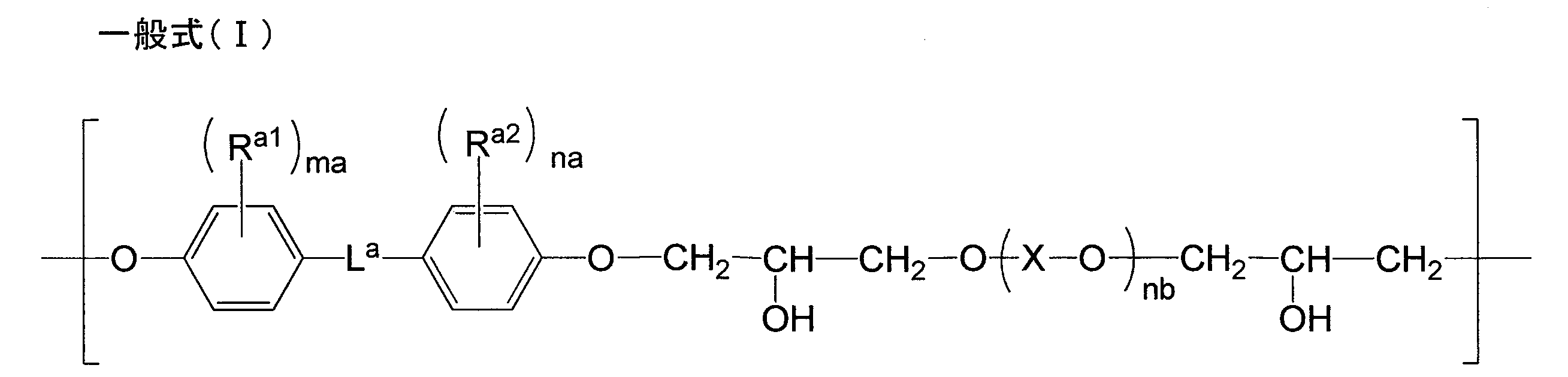
一般式(I)において、La、Ra1、Ra2、maおよびnaは、一般式(A)におけるLa、Ra1、Ra2maおよびnaと同義であり、好ましい範囲も同じである。Xおよびnbは、一般式(B)におけるXおよびnbと同義であり、好ましい範囲も同じである。
本発明では、これらのなかでも、ビスフェノールAと1,6-ヘキサンジオールのジグリシジルエーテルとの重合体が好ましい。
また、フェノキシ樹脂(C)中に僅かに残存するエポキシ基の量は、エポキシ当量で、5000g/eqを越えることが好ましい。
フェノキシ樹脂(C)は、上記のような方法で合成してもよく、また市販品を使用しても構わない。市販品としては、例えば、1256(ビスフェノールA型フェノキシ樹脂、三菱化学(株)製)、YP-50(ビスフェノールA型フェノキシ樹脂、新日化エポキシ製造(株)製)、YP-70(ビスフェノールA/F型フェノキシ樹脂、新日化エポキシ製造(株)製)、FX-316(ビスフェノールF型フェノキシ樹脂、新日化エポキシ製造(株)製)、FX-280S(カルド骨格型フェノキシ樹脂、新日化エポキシ製造(株)製)、4250(ビスフェノールA型/F型フェノキシ樹脂、三菱化学(株)製)等が挙げられる。また、FX-310(低弾性高耐熱型フェノキシ樹脂、新日化エポキシ製造(株)製)等の低弾性高耐熱型フェノキシ樹脂も、好ましく使用することができる。
接着剤層中、エポキシ樹脂(A)とフェノキシ樹脂(C)の各含有量の合計に占めるフェノキシ樹脂(C)の割合は10~60質量%であり、15~50質量%とすることも好ましく、18~45質量%とすることもより好ましい。
接着剤層中、エポキシ樹脂(A)とフェノキシ樹脂(C)の各含有量の合計に占めるフェノキシ樹脂(C)の割合は10~60質量%であり、15~50質量%とすることも好ましく、18~45質量%とすることもより好ましい。
(無機充填剤(D))
上記無機充填剤(D)は、熱伝導性を有する無機充填剤である限り特に制限されない。無機充填剤(D)は、接着剤層に熱伝導性を付与する。
上記無機充填剤(D)は、熱伝導性材料からなる粒子または熱伝導性材料で表面被覆されてなる粒子であって、これらの熱伝導性材料の熱伝導率が12W/m・K以上であることが好ましく、30W/m・K以上であることがより好ましい。
上記熱伝導性材料の熱伝導率が上記好ましい下限値以上であると、目的の熱伝導率を得るために配合する無機充填剤(D)の量を低減することができ、接着剤層の溶融粘度の上昇が抑制されて、基板に圧着する際に基板の凹凸部への埋め込み性をより向上させることができる。結果、ボイドの発生をより確実に抑制できる。
本発明において、上記熱伝導性材料の熱伝導率は、25℃における熱伝導率を意味し、各材料の文献値を用いることができる。文献に記載がない場合にも、例えば、セラミックスであればJIS R 1611により測定される値、金属であれば、JIS H 7801により測定される値を代用することができる。
無機充填剤(D)としては、例えば、熱伝導性のセラミックスがあげられ、アルミナ粒子(熱伝導率:36W/m・K)、窒化アルミニウム粒子(熱伝導率:150~290W/m・K)、窒化ホウ素粒子(熱伝導率:60W/m・K)、酸化亜鉛粒子(熱伝導率:54W/m・K)、窒化ケイ素フィラー(熱伝導率:27W/m・K)、炭化ケイ素粒子(熱伝導率:200W/m・K)および酸化マグネシウム粒子(熱伝導率:59W/m・K)が好ましく挙げられる。
特にアルミナ粒子は高熱伝導率を有し、分散性、入手容易性の点で好ましい。また、窒化アルミニウム粒子や窒化ホウ素粒子は、アルミナ粒子よりもさらに高い熱伝導率を有する観点で好ましい。本発明では、なかでもアルミナ粒子と窒化アルミニウム粒子が好ましい。
また、熱伝導性を有する金属で表面被覆された粒子も挙げられる。例えば、銀(熱伝導率:429W/m・K)、ニッケル(熱伝導率:91W/m・K)及び金(熱伝導率:329W/m・K)等の金属で表面被覆された、シリコーン樹脂粒子及びアクリル樹脂粒子等が好ましく挙げられる。
特に、銀で表面被覆されたシリコーン樹脂粒子は、応力緩和性並びに高耐熱性の観点から好ましい。
特にアルミナ粒子は高熱伝導率を有し、分散性、入手容易性の点で好ましい。また、窒化アルミニウム粒子や窒化ホウ素粒子は、アルミナ粒子よりもさらに高い熱伝導率を有する観点で好ましい。本発明では、なかでもアルミナ粒子と窒化アルミニウム粒子が好ましい。
また、熱伝導性を有する金属で表面被覆された粒子も挙げられる。例えば、銀(熱伝導率:429W/m・K)、ニッケル(熱伝導率:91W/m・K)及び金(熱伝導率:329W/m・K)等の金属で表面被覆された、シリコーン樹脂粒子及びアクリル樹脂粒子等が好ましく挙げられる。
特に、銀で表面被覆されたシリコーン樹脂粒子は、応力緩和性並びに高耐熱性の観点から好ましい。
無機充填剤(D)は、表面処理や表面改質されていてもよく、このような表面処理や表面改質を施すために使用される化合物としては、シランカップリング剤、リン酸もしくはリン酸化合物又は界面活性剤等が挙げられる。本明細書において記載する事項以外は、例えば、国際公開第2018/203527号における熱伝導フィラーの項又は国際公開第2017/158994号の窒化アルミニウム充填剤の項における、シランカップリング剤、リン酸もしくはリン酸化合物及び界面活性剤の記載を適用することができる。
無機充填剤(D)をエポキシ樹脂(A)、エポキシ樹脂硬化剤(B)及びフェノキシ樹脂(C)等の樹脂成分に配合する方法としては、粉体状の無機充填剤と必要に応じてシランカップリング剤、リン酸もしくはリン酸化合物や界面活性剤とを直接配合する方法(インテグラルブレンド法)、もしくはシランカップリング剤、リン酸もしくはリン酸化合物や界面活性剤等の表面処理剤で処理された無機充填剤を、有機溶剤に分散させたスラリー状無機充填剤として配合する方法を使用することができる。
また、シランカップリング剤により無機充填剤(D)を処理する方法としては特に限定されず、溶媒中で無機充填剤(D)とシランカップリング剤を混合する湿式法、気相中で無機充填剤(D)とシランカップリング剤を処理させる乾式法、上記インテグラルブレンド法などが挙げられる。
また、シランカップリング剤により無機充填剤(D)を処理する方法としては特に限定されず、溶媒中で無機充填剤(D)とシランカップリング剤を混合する湿式法、気相中で無機充填剤(D)とシランカップリング剤を処理させる乾式法、上記インテグラルブレンド法などが挙げられる。
特に、窒化アルミニウム粒子は、高熱伝導化に貢献するものの、加水分解によりアンモニウムイオンを生成しやすいため、吸湿率が小さいフェノール樹脂と併用したり、表面改質により加水分解が抑制されていることが好ましい。窒化アルミニウム粒子の表面改質方法としては、表面層に酸化アルミニウムの酸化物層を設け耐水性を向上させ、リン酸もしくはリン酸化合物による表面処理を行い樹脂との親和性を向上させる方法が特に好ましい。
無機充填剤(D)の表面をシランカップリング剤で表面処理することも好ましい。
また、さらにイオントラップ剤を併用することも好ましい。
また、さらにイオントラップ剤を併用することも好ましい。
シランカップリング剤は、ケイ素原子にアルコキシ基、アリールオキシ基のような加水分解性基が少なくとも1つ結合した化合物であり、これに加えて、アルキル基、アルケニル基、アリール基が結合してもよい。アルキル基は、アミノ基、アルコキシ基、エポキシ基又は(メタ)アクリロイルオキシ基で置換されたアルキル基が好ましく、アミノ基(好ましくはフェニルアミノ基)、アルコキシ基(好ましくはグリシジルオキシ基)又は(メタ)アクリロイルオキシ基で置換されたアルキル基がより好ましい。
シランカップリング剤は、例えば、2-(3,4-エポキシシクロへキシル)エチルトリメトキシシラン、3-グリシジルオキシプロピルトリメトキシシラン、3-グリシジルオキシプロピルトリエトキシシラン、3-グリシジルオキシプロピルメチルジメトキシシラン、3-グリシジルオキシプロピルメチルジエトキシシラン、ジメチルジメトキシシラン、ジメチルジエトキシシラン、メチルトリメトキシシラン、メチルトリエトキシシラン、フェニルトリメトキシシラン、フェニルトリエトキシシラン、N-フェニル-3-アミノプロピルトリメトキシシラン、3-メタクリロイルオキプロピルメチルジメトキシシラン、3-メタクリロイルオキプロピルトリメトキシシラン、3-メタクリロイルオキプロピルメチルジエトキシシラン、3-メタクリロイルオキプロピルトリエトキシシランなどが挙げられる。
シランカップリング剤は、例えば、2-(3,4-エポキシシクロへキシル)エチルトリメトキシシラン、3-グリシジルオキシプロピルトリメトキシシラン、3-グリシジルオキシプロピルトリエトキシシラン、3-グリシジルオキシプロピルメチルジメトキシシラン、3-グリシジルオキシプロピルメチルジエトキシシラン、ジメチルジメトキシシラン、ジメチルジエトキシシラン、メチルトリメトキシシラン、メチルトリエトキシシラン、フェニルトリメトキシシラン、フェニルトリエトキシシラン、N-フェニル-3-アミノプロピルトリメトキシシラン、3-メタクリロイルオキプロピルメチルジメトキシシラン、3-メタクリロイルオキプロピルトリメトキシシラン、3-メタクリロイルオキプロピルメチルジエトキシシラン、3-メタクリロイルオキプロピルトリエトキシシランなどが挙げられる。
シランカップリング剤や界面活性剤は、無機充填剤(D)100質量部に対し、0.1~2.0質量部含有させることが好ましい。
シランカップリング剤や界面活性剤の含有量を上記好ましい範囲とすることにより、無機充填剤(D)の凝集を抑制ながら、過剰なシランカップリング剤や界面活性剤の半導体組立加熱工程(例えばリフロー工程)における揮発に起因する、接着界面での剥離を抑制することができ、ボイドの発生が抑えられ、接着性を向上させることができる。
シランカップリング剤や界面活性剤の含有量を上記好ましい範囲とすることにより、無機充填剤(D)の凝集を抑制ながら、過剰なシランカップリング剤や界面活性剤の半導体組立加熱工程(例えばリフロー工程)における揮発に起因する、接着界面での剥離を抑制することができ、ボイドの発生が抑えられ、接着性を向上させることができる。
無機充填剤(D)の形状は、フレーク状、針状、フィラメント状、球状、鱗片状のものが挙げられるが、高充填化及び流動性の観点から球状粒子が好ましい。
また、無機充填剤(D)の平均粒径(d50)は、0.1~3.5μmが好ましい。平均粒径(d50)とは、いわゆるメジアン径であり、レーザー回折・散乱法により粒度分布を測定し、累積分布において粒子の全体積を100%としたときに50%累積となるときの粒径を意味する。
また、無機充填剤(D)の平均粒径(d50)は、0.1~3.5μmが好ましい。平均粒径(d50)とは、いわゆるメジアン径であり、レーザー回折・散乱法により粒度分布を測定し、累積分布において粒子の全体積を100%としたときに50%累積となるときの粒径を意味する。
本発明に用いる接着剤層は、エポキシ樹脂(A)、エポキシ樹脂硬化剤(B)、フェノキシ樹脂(C)および無機充填剤(D)の各含有量の合計に占める無機充填剤(D)の割合が、30~70体積%である。上記無機充填剤(D)の含有割合が上記下限値以上であると、フィルム状接着剤に所望とする熱伝導率及び溶融粘度を付与することができ、半導体パッケージからの放熱効果が得られ、フィルム状接着剤のはみ出し不良も抑制することができる。また、上記上限値以下であると、フィルム状接着剤に所望とする溶融粘度を付与することができ、ボイドの発生を抑制することができる。また、熱変化時に半導体パッケージに生じる内部応力を緩和することもでき、接着力も向上させることができる。
成分(A)~(D)の各含有量の合計に占める無機充填剤(D)の割合は、20~60体積%が好ましく、20~50体積%がより好ましい。
上記無機充填剤(D)の含有量(体積%)は、各成分(A)~(D)の含有質量と比重から算出することができる。
成分(A)~(D)の各含有量の合計に占める無機充填剤(D)の割合は、20~60体積%が好ましく、20~50体積%がより好ましい。
上記無機充填剤(D)の含有量(体積%)は、各成分(A)~(D)の含有質量と比重から算出することができる。
(その他の成分)
本発明に用いる接着剤層は、エポキシ樹脂(A)、エポキシ樹脂硬化剤(B)、フェノキシ樹脂(C)および無機充填剤(D)の他に、本発明の効果を損なわない範囲で、高分子化合物を含有してもよい。
高分子化合物としては、例えば、天然ゴム、ブチルゴム、イソプレンゴム、クロロプレンゴム、シリコーンゴム、エチレン-酢酸ビニル共重合体、エチレン-(メタ)アクリル酸共重合体、エチレン-(メタ)アクリル酸エステル共重合体、ポリブタジエン樹脂、ポリカーボネート樹脂、熱可塑性ポリイミド樹脂、6-ナイロンや6,6-ナイロン等のポリアミド樹脂、(メタ)アクリル樹脂、ポリエチレンテレフタレート及びポリブチレンテレフタレート等のポリエステル樹脂、ポリアミドイミド樹脂、フッ素樹脂等が挙げられる。これらの高分子化合物は単独で用いてもよく、また2種以上を組み合わせて用いてもよい。
また、本発明に用いる接着剤層は、イオントラップ剤(イオン捕捉剤)、硬化触媒、粘度調整剤、酸化防止剤、難燃剤、着色剤等をさらに含有していてもよい。例えば、国際公開第2017/158994号のその他の添加物を含むことができる。
本発明に用いる接着剤層中に占める、エポキシ樹脂(A)、エポキシ樹脂硬化剤(B)、フェノキシ樹脂(C)および無機充填剤(D)の含有量の合計の割合は、例えば、60質量%以上とすることができ、70質量%以上が好ましく、80質量%以上がさらに好ましく、90質量%以上とすることもできる。また、上記割合は100質量%でもよく、95質量%以下とすることもできる。
(接着剤層の特性)
-熱硬化後の熱伝導率-
本発明に用いる接着剤層は、熱硬化後において、熱伝導率が1.0W/m・K以上である。熱伝導率は、1.4W/m・K以上が好ましい。熱伝導率が上記下限値未満であると、発生した熱をパッケージ外部へ逃がしにくくなる傾向にある。本発明の熱伝導性フィルム状接着剤は熱硬化後にこのような優れた熱伝導率を発揮することにより、本発明の熱伝導性フィルム状接着剤を半導体ウェハや配線基板等の被着体に密着させ、熱硬化することによって、半導体パッケージ外部への放熱効率が向上された半導体パッケージを得ることができる。
熱伝導率の上限は、特に限定されるものではないが、通常は30W/m・K以下である。
ここで、熱伝導率の測定における熱硬化後とは、接着剤層の硬化が完了した状態を意味する。具体的には、昇温速度10℃/分でDSC(示差走査熱量計)測定を行った際に反応熱ピークが見られなくなった状態をいう。
本発明において、このような熱硬化後の接着剤層の熱伝導率とは、熱伝導率測定装置(商品名:HC-110、英弘精機(株)製)を用いて、熱流計法(JIS-A1412に準拠)により熱伝導率を測定した値をいう。具体的には、実施例に記載の測定方法を参照することができる。上記熱伝導率は、単位をW/m・Kとした際の小数第1位までを有効とする。
熱伝導率は、無機充填剤(D)の含有量、さらには、無機充填剤(D)の種類に加え、エポキシ樹脂(A)、エポキシ樹脂硬化剤(B)及びフェノキシ樹脂(C)等の共存する化合物もしくは樹脂の種類やこれらの含有量により、上記の範囲へと調整することができる。このことは、下記の硬化前弾性率や溶融粘度についても同様である。
-硬化前弾性率-
本発明に用いる接着剤層は、ピックアップ性を高める観点から、熱硬化前の接着剤層を25℃から5℃/分の昇温速度で昇温したとき、25~80℃の範囲における硬化前弾性率G’が10kPa以上であることが好ましい。また、上記測定条件において、25℃における硬化前弾性率は400kPa以上が好ましく、450kPa以上がより好ましく、500kPa以上がさらに好ましく、600kPa以上とすることも好ましい。また、上記測定条件において、80℃における硬化前弾性率は12kPa以上が好ましく、15kPa以上とすることもより好ましく、20kPa以上とすることもさらに好ましい。
硬化前弾性率G’は、後述する実施例に記載の方法により決定することができる。上記硬化前弾性率G’は、単位をkPaとした際の1の位までを有効とする。
本発明において、熱硬化前の接着剤層とは、接着剤層形成後、25℃以上の温度条件下に曝されていない接着剤層を意味する。本発明のダイシングダイアタッチフィルムは、通常、10℃以下の温度条件下で保管されるため、上記の熱硬化前の接着剤層とは、通常、接着剤層を形成後、10℃以下の温度で保存(保管)されている接着剤層を意味する。
(溶融粘度)
本発明に用いる接着剤層は、ダイアタッチ性を高める観点から、熱硬化前の接着剤層を25℃から5℃/分の昇温速度で昇温したとき、120℃における溶融粘度が500~10000Pa・sの範囲にあることが好ましく、1000~10000Pa・sの範囲にあることがより好ましく、1500~9200Pa・sの範囲にあることがさらに好ましい。
溶融粘度は、後述する実施例に記載の方法により決定することができる。上記溶融粘度は、単位をPa・sとした際の10の位までを有効とする。
本発明に用いる接着剤層は、ダイアタッチ性を高める観点から、熱硬化前の接着剤層を25℃から5℃/分の昇温速度で昇温したとき、120℃における溶融粘度が500~10000Pa・sの範囲にあることが好ましく、1000~10000Pa・sの範囲にあることがより好ましく、1500~9200Pa・sの範囲にあることがさらに好ましい。
溶融粘度は、後述する実施例に記載の方法により決定することができる。上記溶融粘度は、単位をPa・sとした際の10の位までを有効とする。
(接着剤層の形成)
本発明に用いる接着剤層は、接着剤層の構成成分を含有する接着剤層形成用組成物(ワニス)を調製し、この組成物を、離型処理された剥離フィルム上に塗布し、乾燥させて形成することができる。接着剤層形成用組成物は、通常は溶媒を含有する。
接着剤層の厚みは200μm以下が好ましく、100μm以下がより好ましく、50μm以下がさらに好ましく、30μm以下とすることも好ましく、20μm以下とすることも好ましい。接着剤層の厚みは通常は1μm以上であり、2μm以上とすることも好ましく、4μm以上としてもよい。
フィルム状接着剤の厚みは、接触・リニアゲージ方式(卓上型接触式厚み計測装置)により測定することができる。
離型処理された剥離フィルムとしては、得られるフィルム状接着剤のカバーフィルムとして機能するものであればよく、公知のものを適宜採用することができる。例えば、離型処理されたポリプロピレン(PP)、離型処理されたポリエチレン(PE)、離型処理されたポリエチレンテレフタレート(PET)が挙げられる。塗工方法としては、公知の方法を適宜採用することができ、例えば、ロールナイフコーター、グラビアコーター、ダイコーター、リバースコーター等を用いた方法が挙げられる。
接着剤層は、ウェハと貼り合わせる面の算術平均粗さRaが3.0μm以下であることが好ましく、被着体と貼り合わせるいずれの側の表面の算術平均粗さRaも3.0μm以下であることがより好ましい。
上記の算術平均粗さRaは、2.0μm以下であることがより好ましく、1.5μm以下であることがさらに好ましい。下限値は特に制限はないが、0.1μm以上であることが実際的である。
<粘着剤層>
本発明のダイシングダイアタッチフィルムを構成する粘着剤層及びその形成方法は、ダイシングフィルム(ダイシングテープ)として用いられる一般的な構成、方法を適宜に適用することができる。粘着剤層を構成する粘着剤としては、粘着フィルム用途に用いられる一般的な粘着剤、例えば、アクリル系粘着剤、ゴム系粘着剤等を適宜に用いることができる。なかでも、粘着剤層はエネルギー線硬化性であることが好ましい。
本発明のダイシングダイアタッチフィルムを構成する粘着剤層及びその形成方法は、ダイシングフィルム(ダイシングテープ)として用いられる一般的な構成、方法を適宜に適用することができる。粘着剤層を構成する粘着剤としては、粘着フィルム用途に用いられる一般的な粘着剤、例えば、アクリル系粘着剤、ゴム系粘着剤等を適宜に用いることができる。なかでも、粘着剤層はエネルギー線硬化性であることが好ましい。
上記アクリル系粘着剤としては、例えば(メタ)アクリル酸およびそのエステルで構成される樹脂、(メタ)アクリル酸およびそのエステルとこれらと共重合可能な不飽和単量体(例えば酢酸ビニル、スチレン、アクリルニトリル等)との共重合体等が用いられる。また、これらの樹脂を2種類以上混合して用いてもよい。これらの中でも、構成成分として、(メタ)アクリル酸メチル、(メタ)アクリル酸エチルヘキシルおよび(メタ)アクリル酸ブチルから選ばれる1種以上と、(メタ)アクリル酸ヒドロキシエチルおよび酢酸ビニルから選ばれる1種以上とを含む共重合体が好ましい。これにより、被着体との密着性や粘着性の制御が容易になる。
本発明に用いる粘着剤層をエネルギー線硬化性とするために、粘着剤層を構成するポリマー中に重合性基(例えば炭素-炭素不飽和結合)を導入したり、粘着剤層中に重合性モノマーを配合したりすることができる。この重合性モノマーは、重合性基を2つ以上(好ましくは3つ以上)有することが好ましい。すなわち、エネルギー線硬化性とは、エネルギー線の照射により硬化する特性を備えることを意味する。
エネルギー線としては、例えば、紫外線、電子線等が挙げられる。
エネルギー線としては、例えば、紫外線、電子線等が挙げられる。
本発明に用いる粘着剤層として、例えば、特開2010-232422号公報、特許第2661950号公報、特開2002-226796号公報、特開2005-303275号公報等の記載を参照することができる。
粘着剤層の厚さは、1~200μmが好ましく、2~100μmがより好ましく、3~50μmがさらに好ましく、5~30μmとすることも好ましい。
本発明のダイシングダイアタッチフィルムは、接着剤層と粘着剤層との間の25~80℃の範囲における剥離力が0.40N/25mm以下である。この剥離力は、粘着剤層がエネルギー線硬化性の場合には、エネルギー線照射後の接着剤層と粘着剤層との間の剥離力である。接着剤層と粘着剤層との間の25℃における剥離力は0.30N/25mm以下が好ましく、0.20N/25mm以下がより好ましい。また、接着剤層と粘着剤層との間の80℃における剥離力は0.35N/25mm以下が好ましい。
上記剥離力は、実施例に記載の方法により決定することができる。上記剥離力は、単位をN/25mmとした際の小数第2位までを有効とする。
上記剥離力は、実施例に記載の方法により決定することができる。上記剥離力は、単位をN/25mmとした際の小数第2位までを有効とする。
<ダイシングダイアタッチフィルムの作製>
本発明のダイシングダイアタッチフィルムの作製方法は、接着剤層と粘着剤層とを積層した構造とできれば特に制限されない。
例えば、離型処理した剥離ライナー上に粘着剤を含む塗布液を塗布し、乾燥することにより粘着剤層を形成し、粘着剤層と基材フィルムとを貼り合わせることによって、基材フィルム、粘着剤層、剥離ライナーが順に積層されたフィルム(ダイシングフィルム)を作製する。これとは別に、剥離フィルム上に接着剤層形成用組成物を塗布し、乾燥して剥離フィルム上に接着剤層を形成することによって、ダイアタッチフィルムを作製する。次いで、剥離ライナーを剥がして露出させた粘着剤層と接着剤層とが接するようにして、ダイシングフィルムとダイアタッチフィルムを貼り合わせることによって、基材フィルム、粘着剤層、接着剤層、剥離フィルムが順に積層されたダイシングダイアタッチフィルムを得ることができる。
上記のダイシングフィルムとダイアタッチフィルムとの貼り合わせは、加圧条件下で行うことが好ましい。
上記のダイシングフィルムとダイアタッチフィルムとの貼り合わせにおいて、ダイシングフィルムの形状は、リングフレームの開口部を覆うことができる限り特に制限されないが、円形状であることが好ましく、ダイアタッチフィルムの形状は、ウェハの裏面を覆うことができる限り特に制限されないが、円形状であることが好ましい。ダイシングフィルムはダイアタッチフィルムよりも大きく、接着剤層の周囲に粘着剤層が露出した部分を有する形状であることが好ましい。このように、所望の形状に裁断されたダイシングフィルム及びダイアタッチフィルムを貼り合わせることが好ましい。
上記のようにして作製したダイシングダイアタッチフィルムは、使用時には、剥離フィルムを剥離して使用する。
[半導体パッケージおよびその製造方法]
次いで、図面を参照しながら本発明の半導体パッケージおよびその製造方法の好適な実施形態について詳細に説明する。なお、以下の説明および図面中、同一または相当する要素には同一の符号を付し、重複する説明は省略する。図1~図7は、本発明の半導体パッケージの製造方法の各工程の好適な一実施形態を示す概略縦断面図である。
次いで、図面を参照しながら本発明の半導体パッケージおよびその製造方法の好適な実施形態について詳細に説明する。なお、以下の説明および図面中、同一または相当する要素には同一の符号を付し、重複する説明は省略する。図1~図7は、本発明の半導体パッケージの製造方法の各工程の好適な一実施形態を示す概略縦断面図である。
本発明の半導体パッケージの製造方法においては、先ず、第1の工程として、図1に示すように、表面に少なくとも1つの半導体回路が形成された半導体ウェハ1の裏面(すなわち、半導体ウェハ1の半導体回路が形成されていない面)に、本発明のダイシングダイアタッチフィルムを接着剤層の側で熱圧着し(すなわち、接着剤層と半導体ウェハの裏面に接するように熱圧着し)、半導体ウェハ1に接着剤層2と粘着剤層3をこの順に設ける。図1では、接着剤層2を粘着剤層3よりも小さく示しているが、両層の大きさ(面積)は、目的に応じて適宜に設定される。熱圧着の条件は、エポキシ樹脂(A)が事実上熱硬化しない温度で行う。例えば、70℃、圧力0.3MPaの条件が挙げられる。
半導体ウェハ1としては、表面に少なくとも1つの半導体回路が形成された半導体ウェハを適宜用いることができ、例えば、シリコンウェハ、SiCウェハ、GaAsウェハ、GaNウェハが挙げられる。本発明のダイシングダイアタッチフィルムを半導体ウェハ1の裏面に設けるには、例えば、ロールラミネーター、マニュアルラミネーターのような公知の装置を適宜用いることができる。
半導体ウェハ1としては、表面に少なくとも1つの半導体回路が形成された半導体ウェハを適宜用いることができ、例えば、シリコンウェハ、SiCウェハ、GaAsウェハ、GaNウェハが挙げられる。本発明のダイシングダイアタッチフィルムを半導体ウェハ1の裏面に設けるには、例えば、ロールラミネーター、マニュアルラミネーターのような公知の装置を適宜用いることができる。
次いで、第2の工程として、図2に示すように、半導体ウェハ1と接着剤層2とを同時にダイシングすることにより、粘着剤層3上に、半導体チップ4と接着剤層2とを備える接着剤層付き半導体チップ5を得る。ダイシングテープ(図示せず)としては特に制限されず、適宜公知のダイシングテープを用いることができる。さらに、ダイシングに用いる装置(図示せず)も特に制限されず、適宜公知のダイシング装置を用いることができる。
次いで、第3の工程として、必要により粘着剤層をエネルギー線で硬化して粘着力を低減し、ピックアップ等により、接着剤層2から粘着剤層3を取り除いた後、図3に示すように、接着剤層付き半導体チップ5と配線基板6とを接着剤層2を介して熱圧着し、配線基板6に接着剤層付き半導体チップ5を実装する。配線基板6としては、表面に半導体回路が形成された基板を適宜用いることができ、例えば、プリント回路基板(PCB)、各種リードフレーム、および、基板表面に抵抗素子やコンデンサー等の電子部品が搭載された基板が挙げられる。
このような配線基板6に接着剤層付き半導体チップ5を実装する方法としては特に制限されず、接着剤層2を利用して接着剤層付き半導体チップ5を配線基板6または配線基板6の表面上に搭載された電子部品に接着させることが可能な従来の方法を適宜採用することができる。
このような配線基板6に接着剤層付き半導体チップ5を実装する方法としては特に制限されず、接着剤層2を利用して接着剤層付き半導体チップ5を配線基板6または配線基板6の表面上に搭載された電子部品に接着させることが可能な従来の方法を適宜採用することができる。
次いで、第4の工程として、接着剤層2を熱硬化させる。熱硬化の温度としては、接着剤層2の熱硬化開始温度以上であれば特に制限がなく、使用するエポキシ樹脂(A)、フェノキシ樹脂(C)及びエポキシ硬化剤(B)の種類により異なるものであり、一概に言えるものではないが、例えば、100~180℃が好ましく、より高温にて硬化した方が短時間で硬化可能である観点から、140~180℃がより好ましい。温度が熱硬化開始温度未満であると、熱硬化が進まず接着剤層2の強度が低下する傾向にあり、他方、上記上限を超えると硬化過程中に接着剤層2中のエポキシ樹脂、硬化剤や添加剤等が揮発して発泡しやすくなる傾向にある。また、硬化処理の時間は、例えば、10~120分間が好ましい。
次いで、本発明の半導体パッケージの製造方法では、図4に示すように、配線基板6と接着剤層付き半導体チップ5とをボンディングワイヤー7を介して接続することが好ましい。このような接続方法としては特に制限されず、従来公知の方法、例えば、ワイヤーボンディング方式の方法、TAB(Tape Automated Bonding)方式の方法等を適宜採用することができる。
また、搭載された半導体チップ4の表面に、別の半導体チップ4を熱圧着、熱硬化し、再度ワイヤーボンディング方式により配線基板6と接続することにより、複数個積層することもできる。例えば、図5に示すように半導体チップをずらして積層する方法、もしくは図6に示すように2層目以降の接着剤層2を厚くすることで、ボンディングワイヤー7を埋め込みながら積層する方法等がある。
本発明の半導体パッケージの製造方法では、図7に示すように、封止樹脂8により配線基板6と接着剤層付き半導体チップ5とを封止することが好ましく、このようにして半導体パッケージ9を得ることができる。封止樹脂8としては特に制限されず、半導体パッケージの製造に用いることができる適宜公知の封止樹脂を用いることができる。また、封止樹脂8による封止方法としても特に制限されず、適宜公知の方法を採用することが可能である。
本発明の半導体パッケージは、半導体チップと配線基板、又は、半導体チップ間が本発明のダイシングダイアタッチフィルムが有する接着剤層の熱硬化体により接着されてなる。
本発明の半導体パッケージの一例としては、図4及び図7に示すように、半導体チップ4と配線基板6が、本発明のダイシングダイアタッチフィルムが有する接着剤層の熱硬化体により接着されてなる構造を有する半導体パッケージ9(図7においては当該構造を封止した形態の半導体パッケージ9)が挙げられる。また、本発明の半導体パッケージの別の例としては、図5及び図6に示すように、半導体チップ4と配線基板6の接着に加えて、半導体チップ4間が、本発明のダイシングダイアタッチフィルムが有する接着剤層の熱硬化体により接着されてなる構造を有する半導体パッケージ9が挙げられる。
また、半導体チップを多段積層する際の半導体チップ間の接着に本発明のダイシングダイアタッチフィルムにおける接着剤層を用いることにより、半導体チップ間が本発明のダイシングダイアタッチフィルムが有する接着剤層の熱硬化体により接着されてなる構造を有する半導体パッケージが得られる。この場合、半導体チップと配線基板との接着は、本発明のダイシングダイアタッチフィルムが有する接着剤層の熱硬化体により接着(例えば、図5及び図6)されていてもよく、熱伝導性接着剤層として通常用いられる接着剤層により接着されていてもよい。ただし、本発明のダイシングダイアタッチフィルムが有する接着剤層2の熱硬化体により接着されていることが好ましい。
なお、図4~7に記載された構造を有する半導体パッケージ9おいては、半導体チップ4と配線基板6の間、及び、半導体チップ4間に記載する接着剤層2は、熱硬化された状態、すなわち接着剤層の熱硬化体として各部材を接着した状態で存在する。
以下、実施例及び比較例に基づいて本発明をより具体的に説明するが、本発明は以下の実施例に限定されるものではない。また、室温とは25℃を意味し、MEKはメチルエチルケトン、PETはポリエチレンテレフタレートである。
(実施例1)
[1.粘着剤層(ダイシングフィルム)の作製]
(1)基材フィルムの作製
低密度ポリエチレン(LDPE、密度0.92g/cm3、融点110℃)の樹脂ペレットを230℃で溶融し、押出機を用いて厚さ70μmの長尺フィルム状に成形した。得られたフィルムに100kGyの電子線を照射し、基材フィルムを作製した。
[1.粘着剤層(ダイシングフィルム)の作製]
(1)基材フィルムの作製
低密度ポリエチレン(LDPE、密度0.92g/cm3、融点110℃)の樹脂ペレットを230℃で溶融し、押出機を用いて厚さ70μmの長尺フィルム状に成形した。得られたフィルムに100kGyの電子線を照射し、基材フィルムを作製した。
(2)粘着剤層の作製
ブチルアクリレートが50モル%、2-ヒドロキシエチルアクリレートが45モル%およびメタクリル酸が5モル%からなる、質量平均分子量80万の共重合体を調製した。ヨウ素価が20となるように、2-イソシアナトエチルメタクリレートを添加して、ガラス転移温度-40℃、水酸基価30mgKOH/g、酸価5mgKOH/gのアクリル系共重合体を調製した。
次に、上記で調製したアクリル系共重合体100質量部に対して、ポリイソシアネートとしてコロネートL(商品名、日本ポリウレタン製)を5質量部加え、光重合開始剤としてEsacure KIP 150(商品名、Lamberti社製)を3質量部加えた混合物を、酢酸エチルに溶解させ、攪拌して粘着剤組成物を調製した。
次に、離型処理したポリエチレンテレフタレート(PET)フィルムよりなる剥離ライナー上に、この粘着剤組成物を乾燥後の厚さが20μmになるように塗工し、110℃で3分間乾燥させて粘着剤層を形成した後、上記で調製した基材フィルムと粘着剤層とを貼り合わせ、基材フィルム上に粘着剤層が形成されたダイシングフィルムを作製した。
[2.接着剤層(ダイアタッチフィルム)の作製]
トリフェニルメタン型エポキシ樹脂(商品名:EPPN-501H、質量平均分子量:1000、軟化点:55℃、半固体、エポキシ当量:167g/eq、日本化薬(株)製)56質量部、ビスフェノールA型エポキシ樹脂(商品名:YD-128、質量平均分子量:400、軟化点:25℃未満、液体、エポキシ当量:190g/eq、新日化エポキシ製造(株)製)49質量部、ビスフェノールA型フェノキシ樹脂(商品名:YP-50、質量平均分子量:70000、Tg:84℃、常温(25℃)弾性率:1700MPa、新日化エポキシ製造(株)製)30質量部及びMEK67質量部を1000mlのセパラブルフラスコ中において温度110℃で2時間加熱攪拌し、樹脂ワニスを得た。
次いで、この樹脂ワニスを800mlのプラネタリーミキサーに移し、アルミナフィラー(商品名:AO-502、(株)アドマテックス製、平均粒径(d50):0.6μm)205質量部を添加して、イミダゾール型硬化剤(商品名:2PHZ-PW、四国化成(株)製)8.5質量部、シランカップリング剤(商品名:サイラエースS-510、JNC株式会社製)3.0質量部を加えて室温において1時間攪拌混合後、真空脱泡して混合ワニスを得た。
次いで、得られた混合ワニスを厚み38μmの離型処理されたPETフィルム(剥離フィルム)上に塗布して、130℃で10分間加熱乾燥し、縦300mm、横200mm、厚みが10μmの接着剤層が剥離フィルム上に形成されたダイアタッチフィルムを作製した。厚みは、上述の方法により測定した値である。
[3.ダイシングダイアタッチフィルムの作製]
次いで、ダイシングフィルムをリングフレームの開口部を覆うように貼り合わせることができるような円形状に裁断した。また、ダイアタッチフィルムをウェハ裏面を覆うことができるような円形状に裁断した。
上記のように裁断したダイシングフィルムから剥離ライナーを剥離して露出させた粘着剤層と、上記のように裁断したダイアタッチフィルムの接着剤層とを、ロールプレス機を用いて、荷重0.4MPa、速度1.0m/minの条件にて貼り合わせ、ダイシングダイアタッチフィルムを作製した。このダイシングダイアタッチフィルムは、ダイシングフィルムがダイアタッチフィルムよりも大きく、接着剤層の周囲に粘着剤層が露出した部分を有する。
(実施例2)
アルミナフィラー(商品名:AO-502、(株)アドマテックス製、平均粒径(d50):0.6μm)320質量部を使用する以外は実施例1と同様にしてダイシングダイアタッチフィルムを作製した。
アルミナフィラー(商品名:AO-502、(株)アドマテックス製、平均粒径(d50):0.6μm)320質量部を使用する以外は実施例1と同様にしてダイシングダイアタッチフィルムを作製した。
(実施例3)
アルミナフィラー(商品名:AO-502、(株)アドマテックス製、平均粒径(d50):0.6μm)480質量部を使用する以外は実施例1と同様にしてダイシングダイアタッチフィルムを作製した。
アルミナフィラー(商品名:AO-502、(株)アドマテックス製、平均粒径(d50):0.6μm)480質量部を使用する以外は実施例1と同様にしてダイシングダイアタッチフィルムを作製した。
(実施例4)
ビスフェノールA型フェノキシ樹脂に代えてビスフェノールA・F共重合型フェノキシ樹脂(商品名:YP-70、質量平均分子量:55000、Tg:72℃、常温(25℃)弾性率:1400MPa、新日化エポキシ製造(株)製)30質量部を使用する以外は実施例1と同様にしてダイシングダイアタッチフィルムを作製した。
ビスフェノールA型フェノキシ樹脂に代えてビスフェノールA・F共重合型フェノキシ樹脂(商品名:YP-70、質量平均分子量:55000、Tg:72℃、常温(25℃)弾性率:1400MPa、新日化エポキシ製造(株)製)30質量部を使用する以外は実施例1と同様にしてダイシングダイアタッチフィルムを作製した。
(実施例5)
ビスフェノールA型フェノキシ樹脂に代えて低弾性高耐熱型フェノキシ樹脂(商品名:FX-310、質量平均分子量:40000、Tg:110℃、常温(25℃)弾性率:500MPa、新日化エポキシ製造(株)製)30質量部を使用する以外は実施例1と同様にしてダイシングダイアタッチフィルムを作製した。
ビスフェノールA型フェノキシ樹脂に代えて低弾性高耐熱型フェノキシ樹脂(商品名:FX-310、質量平均分子量:40000、Tg:110℃、常温(25℃)弾性率:500MPa、新日化エポキシ製造(株)製)30質量部を使用する以外は実施例1と同様にしてダイシングダイアタッチフィルムを作製した。
(実施例6)
ビスフェノールA型フェノキシ樹脂(商品名:YP-50、質量平均分子量:70000、Tg:84℃、常温(25℃)弾性率:1700MPa、新日化エポキシ製造(株)製)44質量部、アルミナフィラー(商品名:AO-502、(株)アドマテックス製、平均粒径(d50):0.6μm)350質量部を使用する以外は実施例1と同様にしてダイシングダイアタッチフィルムを作製した。
ビスフェノールA型フェノキシ樹脂(商品名:YP-50、質量平均分子量:70000、Tg:84℃、常温(25℃)弾性率:1700MPa、新日化エポキシ製造(株)製)44質量部、アルミナフィラー(商品名:AO-502、(株)アドマテックス製、平均粒径(d50):0.6μm)350質量部を使用する以外は実施例1と同様にしてダイシングダイアタッチフィルムを作製した。
(実施例7)
ビスフェノールA型フェノキシ樹脂(商品名:YP-50、質量平均分子量:70000、Tg:84℃、常温(25℃)弾性率:1700MPa、新日化エポキシ製造(株)製)70質量部、アルミナフィラー(商品名:AO-502、(株)アドマテックス製、平均粒径(d50):0.6μm)400質量部を使用する以外は実施例1と同様にしてダイシングダイアタッチフィルムを作製した。
ビスフェノールA型フェノキシ樹脂(商品名:YP-50、質量平均分子量:70000、Tg:84℃、常温(25℃)弾性率:1700MPa、新日化エポキシ製造(株)製)70質量部、アルミナフィラー(商品名:AO-502、(株)アドマテックス製、平均粒径(d50):0.6μm)400質量部を使用する以外は実施例1と同様にしてダイシングダイアタッチフィルムを作製した。
(実施例8)
ビスフェノールA型フェノキシ樹脂(商品名:YP-50、質量平均分子量:70000、Tg:84℃、常温(25℃)弾性率:1700MPa、新日化エポキシ製造(株)製)50質量部、銀フィラー(商品名:AG-4-8F、(株)DOWAエレクトロニクス製、平均粒径(d50):2.0μm)360質量部を使用する以外は実施例1と同様にしてダイシングダイアタッチフィルムを作製した。
ビスフェノールA型フェノキシ樹脂(商品名:YP-50、質量平均分子量:70000、Tg:84℃、常温(25℃)弾性率:1700MPa、新日化エポキシ製造(株)製)50質量部、銀フィラー(商品名:AG-4-8F、(株)DOWAエレクトロニクス製、平均粒径(d50):2.0μm)360質量部を使用する以外は実施例1と同様にしてダイシングダイアタッチフィルムを作製した。
(実施例9)
ビスフェノールA型フェノキシ樹脂(商品名:YP-50、質量平均分子量:70000、Tg:84℃、常温(25℃)弾性率:1700MPa、新日化エポキシ製造(株)製)50質量部、銀フィラー(商品名:AG-4-8F、(株)DOWAエレクトロニクス製、平均粒径(d50):2.0μm)610質量部を使用する以外は実施例1と同様にしてダイシングダイアタッチフィルムを作製した。
ビスフェノールA型フェノキシ樹脂(商品名:YP-50、質量平均分子量:70000、Tg:84℃、常温(25℃)弾性率:1700MPa、新日化エポキシ製造(株)製)50質量部、銀フィラー(商品名:AG-4-8F、(株)DOWAエレクトロニクス製、平均粒径(d50):2.0μm)610質量部を使用する以外は実施例1と同様にしてダイシングダイアタッチフィルムを作製した。
(実施例10)
ビスフェノールA型フェノキシ樹脂(商品名:YP-50、質量平均分子量:70000、Tg:84℃、常温(25℃)弾性率:1700MPa、新日化エポキシ製造(株)製)50質量部、銀フィラー(商品名:AG-4-8F、(株)DOWAエレクトロニクス製、平均粒径(d50):2.0μm)950質量部を使用する以外は実施例1と同様にしてダイシングダイアタッチフィルムを作製した。
ビスフェノールA型フェノキシ樹脂(商品名:YP-50、質量平均分子量:70000、Tg:84℃、常温(25℃)弾性率:1700MPa、新日化エポキシ製造(株)製)50質量部、銀フィラー(商品名:AG-4-8F、(株)DOWAエレクトロニクス製、平均粒径(d50):2.0μm)950質量部を使用する以外は実施例1と同様にしてダイシングダイアタッチフィルムを作製した。
(比較例1)
ビスフェノールA型フェノキシ樹脂(商品名:YP-50、質量平均分子量:70000、Tg:84℃、常温(25℃)弾性率:1700MPa、新日化エポキシ製造(株)製)10質量部、アルミナフィラー(商品名:AO-502、(株)アドマテックス製、平均粒径(d50):0.6μm)280質量部を使用する以外は実施例1と同様にしてダイシングダイアタッチフィルムを作製した。
ビスフェノールA型フェノキシ樹脂(商品名:YP-50、質量平均分子量:70000、Tg:84℃、常温(25℃)弾性率:1700MPa、新日化エポキシ製造(株)製)10質量部、アルミナフィラー(商品名:AO-502、(株)アドマテックス製、平均粒径(d50):0.6μm)280質量部を使用する以外は実施例1と同様にしてダイシングダイアタッチフィルムを作製した。
(比較例2)
ビスフェノールA型フェノキシ樹脂(商品名:YP-50、質量平均分子量:70000、Tg:84℃、常温(25℃)弾性率:1700MPa、新日化エポキシ製造(株)製)250質量部、アルミナフィラー(商品名:AO-502、(株)アドマテックス製、平均粒径(d50):0.6μm)800質量部を使用する以外は実施例1と同様にしてダイシングダイアタッチフィルムを作製した。
ビスフェノールA型フェノキシ樹脂(商品名:YP-50、質量平均分子量:70000、Tg:84℃、常温(25℃)弾性率:1700MPa、新日化エポキシ製造(株)製)250質量部、アルミナフィラー(商品名:AO-502、(株)アドマテックス製、平均粒径(d50):0.6μm)800質量部を使用する以外は実施例1と同様にしてダイシングダイアタッチフィルムを作製した。
(比較例3)
ビスフェノールA型フェノキシ樹脂(商品名:YP-50、質量平均分子量:70000、Tg:84℃、常温(25℃)弾性率:1700MPa、新日化エポキシ製造(株)製)250質量部、アルミナフィラー(商品名:AO-502、(株)アドマテックス製、平均粒径(d50):0.6μm)130質量部を使用する以外は実施例1と同様にしてダイシングダイアタッチフィルムを作製した。
ビスフェノールA型フェノキシ樹脂(商品名:YP-50、質量平均分子量:70000、Tg:84℃、常温(25℃)弾性率:1700MPa、新日化エポキシ製造(株)製)250質量部、アルミナフィラー(商品名:AO-502、(株)アドマテックス製、平均粒径(d50):0.6μm)130質量部を使用する以外は実施例1と同様にしてダイシングダイアタッチフィルムを作製した。
(比較例4)
ビスフェノールF+1,6-ヘキサンジオールジグリシジルエーテル型フェノキシ樹脂(商品名:YX-7180、質量平均分子量:50000、Tg:15℃、常温(25℃)弾性率:200MPa、三菱ケミカル(株)製)30質量部、アルミナフィラー(商品名:AO-502、(株)アドマテックス製、平均粒径(d50):0.6μm)320質量部を使用する以外は実施例1と同様にしてダイシングダイアタッチフィルムを作製した。
ビスフェノールF+1,6-ヘキサンジオールジグリシジルエーテル型フェノキシ樹脂(商品名:YX-7180、質量平均分子量:50000、Tg:15℃、常温(25℃)弾性率:200MPa、三菱ケミカル(株)製)30質量部、アルミナフィラー(商品名:AO-502、(株)アドマテックス製、平均粒径(d50):0.6μm)320質量部を使用する以外は実施例1と同様にしてダイシングダイアタッチフィルムを作製した。
(比較例5)
アクリルポリマー溶液(商品名:S-2060、質量平均分子量:500000、Tg:-23℃、常温(25℃)弾性率:50MPa、固形分25%(有機溶媒:トルエン)、東亜合成(株)製)120質量部(うちアクリルポリマー自体の配合量は30質量部)、アルミナフィラー(商品名:AO-502、(株)アドマテックス製、平均粒径(d50):0.6μm)320質量部を使用する以外は実施例1と同様にしてダイシングダイアタッチフィルムを作製した。
アクリルポリマー溶液(商品名:S-2060、質量平均分子量:500000、Tg:-23℃、常温(25℃)弾性率:50MPa、固形分25%(有機溶媒:トルエン)、東亜合成(株)製)120質量部(うちアクリルポリマー自体の配合量は30質量部)、アルミナフィラー(商品名:AO-502、(株)アドマテックス製、平均粒径(d50):0.6μm)320質量部を使用する以外は実施例1と同様にしてダイシングダイアタッチフィルムを作製した。
上記で作製した各ダイシングダイアタッチフィルムについて、硬化前弾性率、溶融粘度、剥離力、ダイアタッチ性評価、熱伝導率及び連続ピックアップ性を、それぞれ以下に示す方法により実施した。
得られた結果を接着剤層の組成と共に、下記表1にまとめて示す。
得られた結果を接着剤層の組成と共に、下記表1にまとめて示す。
<硬化前弾性率及び溶融粘度の測定>
上記で作製したダイシングダイアタッチフィルムから縦5.0cm×横5.0cmのサイズの正方形を切り取り、ダイシングフィルム(粘着剤層及び基材フィルム)と剥離フィルムを剥離し、切り取った試料を積層し、ステージ70℃の熱板上で、ハンドローラーにて貼り合わせて、厚さが約1.0mmである接着剤層の試験片を得た。
この試験片について、レオメーター(RS6000、Haake社製)を用い、温度範囲20~250℃、昇温速度5℃/minでの粘性抵抗の変化を測定した。得られた温度-粘性抵抗曲線から、25℃及び80℃における硬化前弾性率G’(kPa)と120℃における溶融粘度(Pa・s)をそれぞれ算出した。
上記で作製したダイシングダイアタッチフィルムから縦5.0cm×横5.0cmのサイズの正方形を切り取り、ダイシングフィルム(粘着剤層及び基材フィルム)と剥離フィルムを剥離し、切り取った試料を積層し、ステージ70℃の熱板上で、ハンドローラーにて貼り合わせて、厚さが約1.0mmである接着剤層の試験片を得た。
この試験片について、レオメーター(RS6000、Haake社製)を用い、温度範囲20~250℃、昇温速度5℃/minでの粘性抵抗の変化を測定した。得られた温度-粘性抵抗曲線から、25℃及び80℃における硬化前弾性率G’(kPa)と120℃における溶融粘度(Pa・s)をそれぞれ算出した。
<剥離力>
上記で作製したダイシングダイアタッチフィルムについて、ダイシングフィルム(粘着剤層)側から紫外線照射装置(商品名:RAD-2000F/8、リンテック株式会社製、照射量200mJ/cm2)を用いて紫外線を照射し、室温及び80℃の恒温槽中において、接着剤層とダイシングフィルム(粘着剤層及び基材フィルム)との層間剥離強度をそれぞれ測定した。
測定条件:JISZ0237準拠、180°剥離試験
測定装置:引張試験機(島津製作所製、型番:TCR1L型)
上記で作製したダイシングダイアタッチフィルムについて、ダイシングフィルム(粘着剤層)側から紫外線照射装置(商品名:RAD-2000F/8、リンテック株式会社製、照射量200mJ/cm2)を用いて紫外線を照射し、室温及び80℃の恒温槽中において、接着剤層とダイシングフィルム(粘着剤層及び基材フィルム)との層間剥離強度をそれぞれ測定した。
測定条件:JISZ0237準拠、180°剥離試験
測定装置:引張試験機(島津製作所製、型番:TCR1L型)
<ダイアタッチ性評価>
上記で作製したダイシングダイアタッチフィルムを、先ず、剥離フィルムを剥がして、マニュアルラミネーター(商品名:FM-114、テクノビジョン社製)を用いて温度70℃、圧力0.3MPaにおいてダミーシリコンウェハ(8inchサイズ、厚さ100μm)の一方の面に接着させた。次いで、2軸のダイシングブレード(Z1:NBC-ZH2050(27HEDD)、DISCO社製/Z2:NBC-ZH127F-SE(BC)、DISCO社製)が設置されたダイシング装置(商品名:DFD-6340、DISCO社製)を用いて、10mm×10mmの正方形のサイズになるようにダミーシリコンウェハ側からダイシングを実施して、接着剤層付きダミーチップを得た。
次いで、ウェハ裏面側から紫外線照射装置(商品名:RAD-2000F/8、リンテック株式会社製、照射量200mJ/cm2)を用いて紫外線を照射し、ダイボンダー(商品名:DB-800、(株)日立ハイテクノロジーズ製)にて120℃、圧力0.1MPa(荷重400gf)、時間1.0秒の条件において、上記接着剤層付きダミーチップをリードフレーム基板(42Arroy系、凸版印刷(株)製)の実装面側と貼り合わせるように、熱圧着した。
基板上に熱圧着した接着剤層付きダミーチップについて、超音波探傷装置(SAT)(日立パワーソリューションズ製 FS300III)を用いて、接着剤層とリードフレーム基板実装面との界面におけるボイドの発生の有無を観察し、下記評価基準に基づき、ダイアタッチ性評価を行った。本発明において、評価「B」以上が合格である。
- 評価基準 -
A:実装したダミーチップ24個の全てにおいてボイドが観察されない。
B:実装したダミーチップ24個のうちボイド発生したチップが1~5個ある。
C:実装したダミーチップ24個のうちボイド発生したチップが6個以上ある。
<熱硬化後の熱伝導率>
上記で作製したダイシングダイアタッチフィルムから一辺50mm以上の四角片を切り取り、ダイシングフィルム(粘着剤層及び基材フィルム)と剥離フィルムとを剥離し、切り取った試料を重ねあわせて厚みが5mm以上の接着剤層積層体を得た。
この試料を、直径50mm、厚さ5mmの円盤状金型の上に置き、圧縮プレス成型機を用いて温度150℃、圧力2MPaにおいて10分間加熱して取り出した後、さらに乾燥機中において温度180℃で1時間加熱することにより接着剤層を熱硬化させ、直径50mm、厚さ5mmの円盤状試験片を得た。
この試験片について、熱伝導率測定装置(商品名:HC-110、英弘精機(株)製)を用いて、熱流計法(JIS-A1412に準拠)により熱伝導率(W/(m・K))を測定した。
<連続ピックアップ性評価>
上記で作製したダイシングダイアタッチフィルムを、先ず、剥離フィルムを剥がして、マニュアルラミネーター(商品名:FM-114、テクノビジョン社製)を用いて温度70℃、圧力0.3MPaにおいてダミーシリコンウェハ(8inchサイズ、厚さ100μm)の一方の面に接着させた。次いで、2軸のダイシングブレード(Z1:NBC-ZH2050(27HEDD)、DISCO社製/Z2:NBC-ZH127F-SE(BC)、DISCO社製)が設置されたダイシング装置(商品名:DFD-6340、DISCO社製)を用いて5mm×5mmの正方形のサイズになるようにダミーシリコンウェハ側からダイシングを実施して、接着剤層付きダミーチップを得た。
次いで、ウェハ裏面側から紫外線照射装置(商品名:RAD-2000F/8、リンテック株式会社製、照射量200mJ/cm2)を用いて紫外線を照射し、ダイボンダー(商品名:DB-800、(株)日立ハイテクノロジーズ製)にて120℃、圧力0.1MPa(荷重400gf)、時間1.0秒の条件において、上記接着剤層付きダミーチップをダイシングフィルム(粘着剤層及び基材フィルム)よりピックアップし、リードフレーム基板(42Arroy系、凸版印刷(株)製)の実装面側と貼り合わせるように、熱圧着した。このピックアップして熱圧着する工程を連続的に繰り返し行い、下記評価基準に基づき、連続ピックアップ性評価を行った。本発明において、評価「B」以上が合格である。
- 評価基準 -
A:連続してピックアップ、熱圧着を行ったダミーチップ96個の全てにおいて、ピックアップミスや、ダイシングフィルム上への接着剤層残り等の不良が見られない。
B:連続してピックアップ、熱圧着を行ったダミーチップ96個のうち、ピックアップミスや、ダイシングフィルム上への接着剤層残り等の不良が発生したチップが1~10個である。
C:連続してピックアップ、熱圧着を行ったダミーチップ96個のうち、ピックアップミスや、ダイシングフィルム上への接着剤層残り等の不良が発生したチップが11個以上である。
<平均粒径(d50)の測定>
上記で用いた各無機充填剤0.1gとMEK9.9gを秤量し、これらの混合物に超音波分散処理を5分行い、測定用試料を調製した。この測定用試料について、レーザー回折・散乱法(型式:LMS-2000e、(株)セイシン企業製)により測定した粒度分布の粒径の体積分率の累積カーブから、平均粒径(d50)を求めた。
上記で用いた各無機充填剤0.1gとMEK9.9gを秤量し、これらの混合物に超音波分散処理を5分行い、測定用試料を調製した。この測定用試料について、レーザー回折・散乱法(型式:LMS-2000e、(株)セイシン企業製)により測定した粒度分布の粒径の体積分率の累積カーブから、平均粒径(d50)を求めた。
<フェノキシ樹脂の常温(25℃)弾性率>
各種フェノキシ樹脂30質量部及びMEK(メチルエチルケトン)70質量部を500mlのセパラブルフラスコ中において、温度110℃で2時間加熱攪拌し、樹脂ワニスを得た。
次いで、この樹脂ワニスを厚み38μmの離型処理されたPETフィルム(剥離フィルム)上に塗布して、130℃で10分間加熱乾燥し、縦300mm、横200mm、厚みが100μmである、フェノキシ樹脂フィルムを得た。
このフェノキシ樹脂フィルムを5mm×17mmのサイズに切り取り、動的粘弾性測定装置(商品名:Rheogel-E4000F、(株)ユービーエム製)を用いて、測定温度範囲0~100℃、昇温速度5℃/min、及び周波数1Hzの条件下で測定を行い、25℃における弾性率の値を求めた。
なお、比較例5で用いたアクリル樹脂についても、フェノキシ樹脂と同様に、上記方法に従って25℃における弾性率を求めた。
<フェノキシ樹脂のガラス転移温度(Tg)>
上記弾性率の測定に記載の方法により作製したフェノキシ樹脂フィルムについて、示差走査熱量計(型番:DSC7000、株式会社日立ハイテクサイエンス製)を用いて、昇温速度5℃/minの条件で測定し、吸熱ピーク側へベースラインがシフトする温度をガラス転移温度(Tg)として測定した。
上記弾性率の測定に記載の方法により作製したフェノキシ樹脂フィルムについて、示差走査熱量計(型番:DSC7000、株式会社日立ハイテクサイエンス製)を用いて、昇温速度5℃/minの条件で測定し、吸熱ピーク側へベースラインがシフトする温度をガラス転移温度(Tg)として測定した。
<質量平均分子量>
各種フェノキシ樹脂について、ゲルパーミエーションクロマトグラフィ(型番:HLC-8320、東ソー株式会社製)を用いて、テトラヒドロフランを溶離液として使用し、流速1ml/min、カラム室の温度を40℃の条件で測定した。質量平均分子量は標準ポリスチレン検量線を用いて算出した。
各種フェノキシ樹脂について、ゲルパーミエーションクロマトグラフィ(型番:HLC-8320、東ソー株式会社製)を用いて、テトラヒドロフランを溶離液として使用し、流速1ml/min、カラム室の温度を40℃の条件で測定した。質量平均分子量は標準ポリスチレン検量線を用いて算出した。
なお、比較例5で用いたアクリル樹脂についても、フェノキシ樹脂と同様に、上記方法に従って、25℃における弾性率、ガラス転移温度、質量平均分子量を求めた。
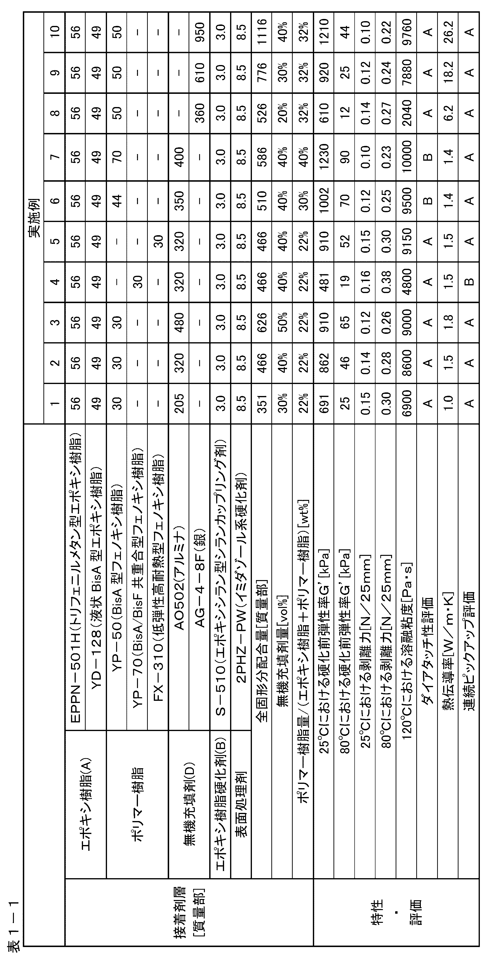
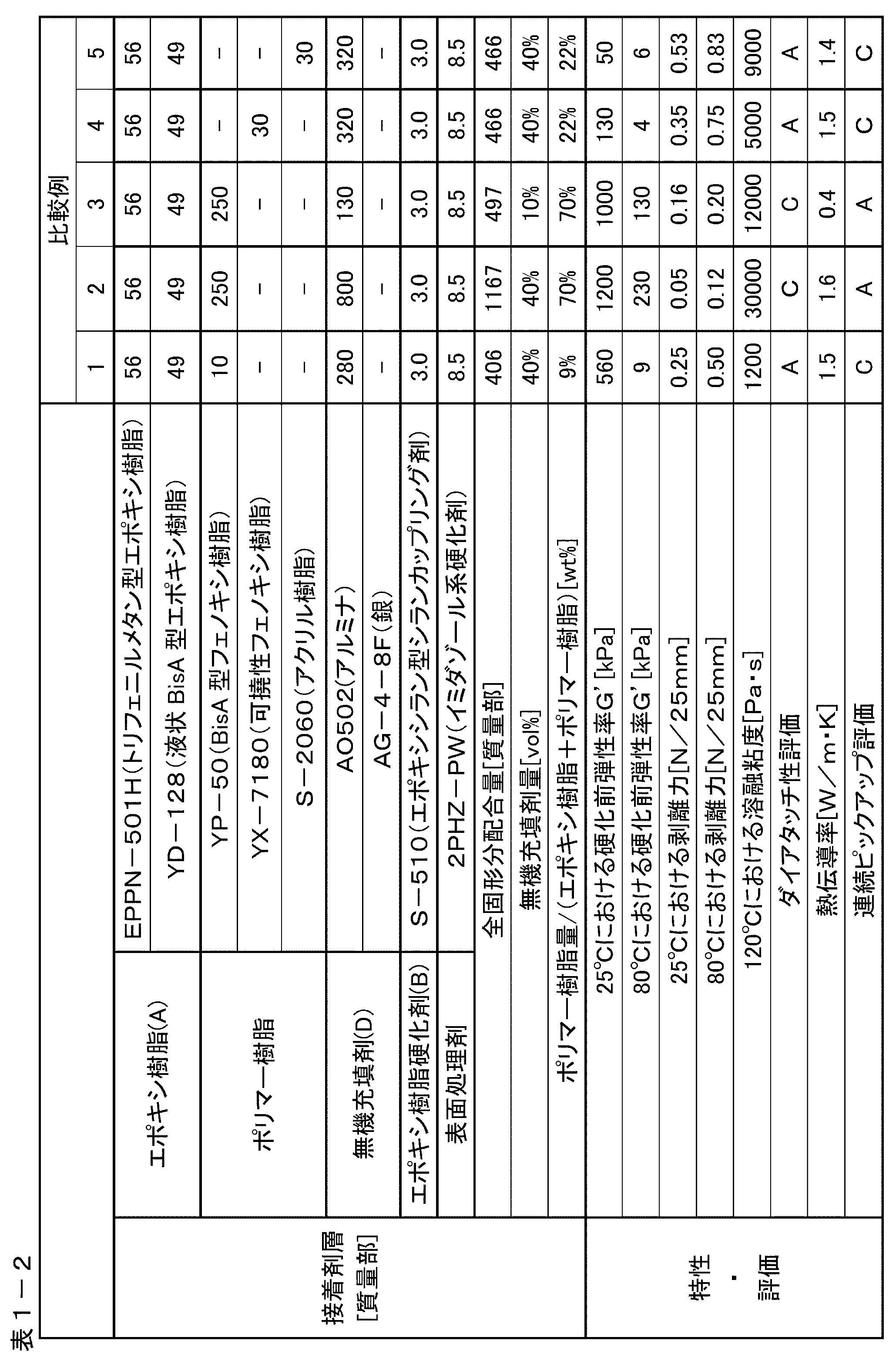
<表の注>
接着剤層の欄における「-」は、その成分を含有していないことを意味する。
接着剤層の欄における「-」は、その成分を含有していないことを意味する。
上記表1から、以下のことがわかる。
比較例1のダイシングダイアタッチフィルムは、エポキシ樹脂(A)とフェノキシ樹脂(C)の各含有量の合計に占めるフェノキシ樹脂(C)の割合が、10質量%未満であり、80℃における接着剤層と粘着剤層との間における剥離力が0.40N/25mm越えである。この比較例1のダイシングダイアタッチフィルムは、ピックアップコレットの蓄熱により、連続してピックアップした際には、96個のチップのうち11個以上のチップでピックアップ不良が生じてしまい、ピックアップ性に劣っていた。
比較例2及び3のダイシングダイアタッチフィルムは、エポキシ樹脂(A)とフェノキシ樹脂(C)の各含有量の合計に占めるフェノキシ樹脂(C)の割合が、60質量%越えである。この比較例2及び3のダイシングダイアタッチフィルムは、配線基板に熱圧着した際に、24個のチップのうち6個以上のチップでボイドが発生してしまい、ボイド発生の抑制が不十分であった。また、比較例3のダイシングダイアタッチフィルムは、熱硬化後の接着剤層の熱伝導率が1.0W/m・K未満と低く、半導体パッケージに適用される接着剤としての放熱性も十分でなかった。
比較例4のダイシングダイアタッチフィルムは、フェノキシ樹脂(C)の25℃における弾性率が500MPa未満である。また、比較例5のダイシングダイアタッチフィルムは、フェノキシ樹脂を含有せず、アクリル樹脂(25℃における弾性率が500MPa未満)を含有する。これらの比較例4及び5のダイシングダイアタッチフィルムは、ピックアップコレットの蓄熱により、連続してピックアップした際には、96個のチップのうち11個以上のチップでピックアップ不良が生じてしまい、ピックアップ性に劣っていた。
これらに対して、本発明の実施例1~10のダイシングダイアタッチフィルムは、半導体加工における連続ピックアップ性に優れ、ピックアップコレットが蓄熱してもピックアップ不良を生じにくかった。また、配線基板に熱圧着した際のボイドの発生の抑制にも優れていた。
本願は、2020年3月13日に日本国で特許出願された特願2020-044660に基づく優先権を主張するものであり、これはここに参照してその内容を本明細書の記載の一部として取り込む。
1 半導体ウェハ
2 接着剤層
3 粘着剤層
4 半導体チップ
5 フィルム状接着剤付き半導体チップ
6 配線基板
7 ボンディングワイヤー
8 封止樹脂
9 半導体パッケージ
2 接着剤層
3 粘着剤層
4 半導体チップ
5 フィルム状接着剤付き半導体チップ
6 配線基板
7 ボンディングワイヤー
8 封止樹脂
9 半導体パッケージ
Claims (6)
- 接着剤層と粘着剤層とが積層されてなるダイシングダイアタッチフィルムであって、
前記接着剤層が、エポキシ樹脂(A)、エポキシ樹脂硬化剤(B)、フェノキシ樹脂(C)及び無機充填材(D)を含有するフィルム状接着剤の層であり、
前記フェノキシ樹脂(C)の25℃における弾性率が500MPa以上であり、
前記接着剤層中、前記エポキシ樹脂(A)と前記フェノキシ樹脂(C)の各含有量の合計に占める前記フェノキシ樹脂(C)の割合が、10~60質量%であり、
前記接着剤層と前記粘着剤層の25~80℃の範囲における剥離力が0.40N/25mm以下であり、
前記接着剤層は、熱硬化後の熱伝導率が1.0W/m・K以上であることを特徴とする、ダイシングダイアタッチフィルム。 - 前記接着剤層を25℃から5℃/分の昇温速度で昇温したとき、25~80℃の範囲における硬化前弾性率G’が10kPa以上であることを特徴とする、請求項1に記載のダイシングダイアタッチフィルム。
- 前記接着剤層を25℃から5℃/分の昇温速度で昇温したとき、120℃における溶融粘度が500~10000Pa・sの範囲にあることを特徴とする、請求項1又は2に記載のダイシングダイアタッチフィルム。
- 前記粘着剤層がエネルギー線硬化性である、請求項1~3のいずれか1項に記載のダイシングダイアタッチフィルム。
- 表面に少なくとも1つの半導体回路が形成された半導体ウェハの裏面に、請求項1~4のいずれか1項に記載のダイシングダイアタッチフィルムを、前記接着剤層を半導体ウェハの裏面に接するように熱圧着して設ける第1の工程と、
前記半導体ウェハと前記接着剤層とを同時にダイシングすることにより、粘着剤層上に、前記半導体チップ及び前記接着剤層を備える接着剤層付き半導体チップを得る第2の工程と、
前記接着剤層から前記粘着剤層を取り除き、前記接着剤層付き半導体チップと配線基板とを前記接着剤層を介して熱圧着する第3の工程と、
前記接着剤層を熱硬化する第4の工程と、
を含むことを特徴とする半導体パッケージの製造方法。 - 半導体チップと配線基板、又は、半導体チップ間が、請求項1~4のいずれか1項に記載のダイシングダイアタッチフィルムが有する接着剤層の熱硬化体により接着されてなることを特徴とする、半導体パッケージ。
Priority Applications (6)
| Application Number | Priority Date | Filing Date | Title |
|---|---|---|---|
| KR1020217005830A KR102477359B1 (ko) | 2020-03-13 | 2020-11-06 | 다이싱 다이 어태치 필름과 이것을 이용한 반도체 패키지 및 그 제조 방법 |
| MYPI2021006815A MY195164A (en) | 2020-03-13 | 2020-11-06 | Dicing Die Attach Film, and Semiconductor Package Using the Same and Method of Producing Semiconductor Package |
| SG11202112233RA SG11202112233RA (en) | 2020-03-13 | 2020-11-06 | Dicing die attach film, and semiconductor package using the same and method of producing semiconductor package |
| CN202080005697.5A CN113874456B (zh) | 2020-03-13 | 2020-11-06 | 切晶粘晶膜、以及使用了该切晶粘晶膜的半导体封装及其制造方法 |
| PH1/2021/552812A PH12021552812A1 (en) | 2020-03-13 | 2020-11-06 | Dicing die attach film, and semiconductor package using the same and method of producing semiconductor package |
| US17/529,388 US12176314B2 (en) | 2020-03-13 | 2021-11-18 | Dicing die attach film, and semiconductor package using the same and method of producing semiconductor package |
Applications Claiming Priority (2)
| Application Number | Priority Date | Filing Date | Title |
|---|---|---|---|
| JP2020044660A JP6902641B1 (ja) | 2020-03-13 | 2020-03-13 | ダイシングダイアタッチフィルム、並びに、ダイシングダイアタッチフィルムを用いた半導体パッケージ及びその製造方法 |
| JP2020-044660 | 2020-03-13 |
Related Child Applications (1)
| Application Number | Title | Priority Date | Filing Date |
|---|---|---|---|
| US17/529,388 Continuation US12176314B2 (en) | 2020-03-13 | 2021-11-18 | Dicing die attach film, and semiconductor package using the same and method of producing semiconductor package |
Publications (1)
| Publication Number | Publication Date |
|---|---|
| WO2021181748A1 true WO2021181748A1 (ja) | 2021-09-16 |
Family
ID=76753137
Family Applications (1)
| Application Number | Title | Priority Date | Filing Date |
|---|---|---|---|
| PCT/JP2020/041623 Ceased WO2021181748A1 (ja) | 2020-03-13 | 2020-11-06 | ダイシングダイアタッチフィルム、並びに、これを用いた半導体パッケージ及びその製造方法 |
Country Status (9)
| Country | Link |
|---|---|
| US (1) | US12176314B2 (ja) |
| JP (1) | JP6902641B1 (ja) |
| KR (1) | KR102477359B1 (ja) |
| CN (1) | CN113874456B (ja) |
| MY (1) | MY195164A (ja) |
| PH (1) | PH12021552812A1 (ja) |
| SG (1) | SG11202112233RA (ja) |
| TW (1) | TWI824195B (ja) |
| WO (1) | WO2021181748A1 (ja) |
Families Citing this family (5)
| Publication number | Priority date | Publication date | Assignee | Title |
|---|---|---|---|---|
| WO2019106846A1 (ja) * | 2017-12-01 | 2019-06-06 | 日立化成株式会社 | 半導体装置の製造方法、仮固定材用樹脂組成物、及び仮固定材用積層フィルム |
| US11996384B2 (en) | 2020-12-15 | 2024-05-28 | Pulseforge, Inc. | Method and apparatus for debonding temporarily bonded wafers in wafer-level packaging applications |
| JP7223090B1 (ja) * | 2021-09-28 | 2023-02-15 | 古河電気工業株式会社 | 接着剤用組成物及びフィルム状接着剤、並びに、フィルム状接着剤を用いた半導体パッケージ及びその製造方法 |
| CN115036255B (zh) * | 2022-06-24 | 2025-06-27 | 中国电子科技集团公司第二十九研究所 | 用于半导体器件引线键合的方法 |
| JP2025038510A (ja) * | 2023-09-07 | 2025-03-19 | 株式会社レゾナック | フィルム状接着剤、接着剤フィルム、接続構造体、及び接続構造体の製造方法 |
Citations (3)
| Publication number | Priority date | Publication date | Assignee | Title |
|---|---|---|---|---|
| JP2012207222A (ja) * | 2011-03-16 | 2012-10-25 | Nippon Steel Chem Co Ltd | 高熱伝導性フィルム状接着剤用組成物、高熱伝導性フィルム状接着剤、並びに、それを用いた半導体パッケージとその製造方法 |
| JP2013157589A (ja) * | 2012-01-06 | 2013-08-15 | Furukawa Electric Co Ltd:The | ウエハ加工用テープ及びこれを使用した半導体装置の製造方法 |
| WO2017158994A1 (ja) * | 2016-03-15 | 2017-09-21 | 古河電気工業株式会社 | フィルム状接着剤用組成物、フィルム状接着剤、フィルム状接着剤の製造方法、フィルム状接着剤を用いた半導体パッケージおよびその製造方法 |
Family Cites Families (8)
| Publication number | Priority date | Publication date | Assignee | Title |
|---|---|---|---|---|
| JPS58173591A (ja) | 1982-04-02 | 1983-10-12 | 松下電器産業株式会社 | ミシン速度設定装置 |
| JP2010232422A (ja) | 2009-03-27 | 2010-10-14 | Sumitomo Bakelite Co Ltd | ダイシングダイアタッチフィルム |
| MY184455A (en) * | 2011-09-16 | 2021-04-01 | Lintec Corp | Base film for dicing sheet and dicing sheet |
| JP6366228B2 (ja) | 2013-06-04 | 2018-08-01 | 日東電工株式会社 | 接着シート、及びダイシング・ダイボンディングフィルム |
| JP5901715B1 (ja) * | 2014-09-05 | 2016-04-13 | 古河電気工業株式会社 | フィルム状接着剤、フィルム状接着剤を用いた半導体パッケージ及びその製造方法 |
| JP6615150B2 (ja) * | 2017-05-01 | 2019-12-04 | 古河電気工業株式会社 | 接着フィルム、半導体ウェハ加工用テープ、半導体パッケージおよびその製造方法 |
| JP6800129B2 (ja) * | 2017-11-07 | 2020-12-16 | 古河電気工業株式会社 | フィルム状接着剤、フィルム状接着剤を用いた半導体パッケージの製造方法 |
| PH12021551244B1 (en) * | 2019-08-22 | 2024-02-07 | Furukawa Electric Co Ltd | Adhesive composition, film-like adhesive and production method thereof, and semiconductor package using film-like adhesive and method for manufacturing same |
-
2020
- 2020-03-13 JP JP2020044660A patent/JP6902641B1/ja active Active
- 2020-11-06 SG SG11202112233RA patent/SG11202112233RA/en unknown
- 2020-11-06 WO PCT/JP2020/041623 patent/WO2021181748A1/ja not_active Ceased
- 2020-11-06 PH PH1/2021/552812A patent/PH12021552812A1/en unknown
- 2020-11-06 KR KR1020217005830A patent/KR102477359B1/ko active Active
- 2020-11-06 CN CN202080005697.5A patent/CN113874456B/zh active Active
- 2020-11-06 MY MYPI2021006815A patent/MY195164A/en unknown
- 2020-11-13 TW TW109139658A patent/TWI824195B/zh active
-
2021
- 2021-11-18 US US17/529,388 patent/US12176314B2/en active Active
Patent Citations (3)
| Publication number | Priority date | Publication date | Assignee | Title |
|---|---|---|---|---|
| JP2012207222A (ja) * | 2011-03-16 | 2012-10-25 | Nippon Steel Chem Co Ltd | 高熱伝導性フィルム状接着剤用組成物、高熱伝導性フィルム状接着剤、並びに、それを用いた半導体パッケージとその製造方法 |
| JP2013157589A (ja) * | 2012-01-06 | 2013-08-15 | Furukawa Electric Co Ltd:The | ウエハ加工用テープ及びこれを使用した半導体装置の製造方法 |
| WO2017158994A1 (ja) * | 2016-03-15 | 2017-09-21 | 古河電気工業株式会社 | フィルム状接着剤用組成物、フィルム状接着剤、フィルム状接着剤の製造方法、フィルム状接着剤を用いた半導体パッケージおよびその製造方法 |
Also Published As
| Publication number | Publication date |
|---|---|
| US12176314B2 (en) | 2024-12-24 |
| US20220077101A1 (en) | 2022-03-10 |
| CN113874456A (zh) | 2021-12-31 |
| JP6902641B1 (ja) | 2021-07-14 |
| SG11202112233RA (en) | 2021-12-30 |
| CN113874456B (zh) | 2023-09-19 |
| PH12021552812A1 (en) | 2022-09-28 |
| TW202134370A (zh) | 2021-09-16 |
| MY195164A (en) | 2023-01-11 |
| TWI824195B (zh) | 2023-12-01 |
| KR102477359B1 (ko) | 2022-12-16 |
| KR20210116414A (ko) | 2021-09-27 |
| JP2021145115A (ja) | 2021-09-24 |
Similar Documents
| Publication | Publication Date | Title |
|---|---|---|
| US11952513B2 (en) | Adhesive composition, film-like adhesive and production method thereof, and semiconductor package using film-like adhesive and production method thereof | |
| JP6902641B1 (ja) | ダイシングダイアタッチフィルム、並びに、ダイシングダイアタッチフィルムを用いた半導体パッケージ及びその製造方法 | |
| JP7178529B1 (ja) | 熱伝導性フィルム状接着剤、半導体パッケージ及びその製造方法 | |
| JP6989721B1 (ja) | ダイシングダイアタッチフィルム及びその製造方法、並びに半導体パッケージ及びその製造方法 | |
| JP7042986B1 (ja) | 接着剤用組成物及びフィルム状接着剤、並びに、フィルム状接着剤を用いた半導体パッケージ及びその製造方法 | |
| US20220310547A1 (en) | Dicing die attach film and method of producing the same, and semiconductor package and method of producing the same | |
| CN115413363B (zh) | 切晶粘晶膜及其制造方法、以及半导体封装及其制造方法 | |
| HK40059508A (en) | Dicing die attach film, semiconductor package using dicing die attach film, and method for manufacturing semiconductor package | |
| HK40077350A (en) | Dicing die attach film and method for producing same, and semiconductor package and method for producing same | |
| HK40059508B (en) | Dicing die attach film, semiconductor package using dicing die attach film, and method for manufacturing semiconductor package | |
| HK40081342A (en) | Dicing die attach film, method for producing same, semiconductor package, and method for producing same | |
| HK40050915A (en) | Adhesive composition, film-like adhesive and production method thereof, and semiconductor package using film-like adhesive and method for manufacturing same |
Legal Events
| Date | Code | Title | Description |
|---|---|---|---|
| ENP | Entry into the national phase |
Ref document number: 20217005830 Country of ref document: KR Kind code of ref document: A |
|
| 121 | Ep: the epo has been informed by wipo that ep was designated in this application |
Ref document number: 20924682 Country of ref document: EP Kind code of ref document: A1 |
|
| NENP | Non-entry into the national phase |
Ref country code: DE |
|
| 122 | Ep: pct application non-entry in european phase |
Ref document number: 20924682 Country of ref document: EP Kind code of ref document: A1 |