WO2021176504A1 - 走査線駆動回路およびこれを備えた表示装置 - Google Patents
走査線駆動回路およびこれを備えた表示装置 Download PDFInfo
- Publication number
- WO2021176504A1 WO2021176504A1 PCT/JP2020/008640 JP2020008640W WO2021176504A1 WO 2021176504 A1 WO2021176504 A1 WO 2021176504A1 JP 2020008640 W JP2020008640 W JP 2020008640W WO 2021176504 A1 WO2021176504 A1 WO 2021176504A1
- Authority
- WO
- WIPO (PCT)
- Prior art keywords
- scanning line
- line drive
- drive circuit
- voltage
- resistor
- Prior art date
- Legal status (The legal status is an assumption and is not a legal conclusion. Google has not performed a legal analysis and makes no representation as to the accuracy of the status listed.)
- Ceased
Links
Images




















Classifications
-
- G—PHYSICS
- G09—EDUCATION; CRYPTOGRAPHY; DISPLAY; ADVERTISING; SEALS
- G09G—ARRANGEMENTS OR CIRCUITS FOR CONTROL OF INDICATING DEVICES USING STATIC MEANS TO PRESENT VARIABLE INFORMATION
- G09G3/00—Control arrangements or circuits, of interest only in connection with visual indicators other than cathode-ray tubes
- G09G3/20—Control arrangements or circuits, of interest only in connection with visual indicators other than cathode-ray tubes for presentation of an assembly of a number of characters, e.g. a page, by composing the assembly by combination of individual elements arranged in a matrix no fixed position being assigned to or needed to be assigned to the individual characters or partial characters
- G09G3/22—Control arrangements or circuits, of interest only in connection with visual indicators other than cathode-ray tubes for presentation of an assembly of a number of characters, e.g. a page, by composing the assembly by combination of individual elements arranged in a matrix no fixed position being assigned to or needed to be assigned to the individual characters or partial characters using controlled light sources
- G09G3/30—Control arrangements or circuits, of interest only in connection with visual indicators other than cathode-ray tubes for presentation of an assembly of a number of characters, e.g. a page, by composing the assembly by combination of individual elements arranged in a matrix no fixed position being assigned to or needed to be assigned to the individual characters or partial characters using controlled light sources using electroluminescent panels
- G09G3/32—Control arrangements or circuits, of interest only in connection with visual indicators other than cathode-ray tubes for presentation of an assembly of a number of characters, e.g. a page, by composing the assembly by combination of individual elements arranged in a matrix no fixed position being assigned to or needed to be assigned to the individual characters or partial characters using controlled light sources using electroluminescent panels semiconductive, e.g. using light-emitting diodes [LED]
- G09G3/3208—Control arrangements or circuits, of interest only in connection with visual indicators other than cathode-ray tubes for presentation of an assembly of a number of characters, e.g. a page, by composing the assembly by combination of individual elements arranged in a matrix no fixed position being assigned to or needed to be assigned to the individual characters or partial characters using controlled light sources using electroluminescent panels semiconductive, e.g. using light-emitting diodes [LED] organic, e.g. using organic light-emitting diodes [OLED]
- G09G3/3266—Details of drivers for scan electrodes
-
- G—PHYSICS
- G09—EDUCATION; CRYPTOGRAPHY; DISPLAY; ADVERTISING; SEALS
- G09F—DISPLAYING; ADVERTISING; SIGNS; LABELS OR NAME-PLATES; SEALS
- G09F9/00—Indicating arrangements for variable information in which the information is built-up on a support by selection or combination of individual elements
-
- G—PHYSICS
- G09—EDUCATION; CRYPTOGRAPHY; DISPLAY; ADVERTISING; SEALS
- G09F—DISPLAYING; ADVERTISING; SIGNS; LABELS OR NAME-PLATES; SEALS
- G09F9/00—Indicating arrangements for variable information in which the information is built-up on a support by selection or combination of individual elements
- G09F9/30—Indicating arrangements for variable information in which the information is built-up on a support by selection or combination of individual elements in which the desired character or characters are formed by combining individual elements
-
- G—PHYSICS
- G09—EDUCATION; CRYPTOGRAPHY; DISPLAY; ADVERTISING; SEALS
- G09G—ARRANGEMENTS OR CIRCUITS FOR CONTROL OF INDICATING DEVICES USING STATIC MEANS TO PRESENT VARIABLE INFORMATION
- G09G3/00—Control arrangements or circuits, of interest only in connection with visual indicators other than cathode-ray tubes
- G09G3/20—Control arrangements or circuits, of interest only in connection with visual indicators other than cathode-ray tubes for presentation of an assembly of a number of characters, e.g. a page, by composing the assembly by combination of individual elements arranged in a matrix no fixed position being assigned to or needed to be assigned to the individual characters or partial characters
- G09G3/22—Control arrangements or circuits, of interest only in connection with visual indicators other than cathode-ray tubes for presentation of an assembly of a number of characters, e.g. a page, by composing the assembly by combination of individual elements arranged in a matrix no fixed position being assigned to or needed to be assigned to the individual characters or partial characters using controlled light sources
- G09G3/30—Control arrangements or circuits, of interest only in connection with visual indicators other than cathode-ray tubes for presentation of an assembly of a number of characters, e.g. a page, by composing the assembly by combination of individual elements arranged in a matrix no fixed position being assigned to or needed to be assigned to the individual characters or partial characters using controlled light sources using electroluminescent panels
- G09G3/32—Control arrangements or circuits, of interest only in connection with visual indicators other than cathode-ray tubes for presentation of an assembly of a number of characters, e.g. a page, by composing the assembly by combination of individual elements arranged in a matrix no fixed position being assigned to or needed to be assigned to the individual characters or partial characters using controlled light sources using electroluminescent panels semiconductive, e.g. using light-emitting diodes [LED]
- G09G3/3208—Control arrangements or circuits, of interest only in connection with visual indicators other than cathode-ray tubes for presentation of an assembly of a number of characters, e.g. a page, by composing the assembly by combination of individual elements arranged in a matrix no fixed position being assigned to or needed to be assigned to the individual characters or partial characters using controlled light sources using electroluminescent panels semiconductive, e.g. using light-emitting diodes [LED] organic, e.g. using organic light-emitting diodes [OLED]
- G09G3/3225—Control arrangements or circuits, of interest only in connection with visual indicators other than cathode-ray tubes for presentation of an assembly of a number of characters, e.g. a page, by composing the assembly by combination of individual elements arranged in a matrix no fixed position being assigned to or needed to be assigned to the individual characters or partial characters using controlled light sources using electroluminescent panels semiconductive, e.g. using light-emitting diodes [LED] organic, e.g. using organic light-emitting diodes [OLED] using an active matrix
- G09G3/3233—Control arrangements or circuits, of interest only in connection with visual indicators other than cathode-ray tubes for presentation of an assembly of a number of characters, e.g. a page, by composing the assembly by combination of individual elements arranged in a matrix no fixed position being assigned to or needed to be assigned to the individual characters or partial characters using controlled light sources using electroluminescent panels semiconductive, e.g. using light-emitting diodes [LED] organic, e.g. using organic light-emitting diodes [OLED] using an active matrix with pixel circuitry controlling the current through the light-emitting element
- G09G3/3241—Control arrangements or circuits, of interest only in connection with visual indicators other than cathode-ray tubes for presentation of an assembly of a number of characters, e.g. a page, by composing the assembly by combination of individual elements arranged in a matrix no fixed position being assigned to or needed to be assigned to the individual characters or partial characters using controlled light sources using electroluminescent panels semiconductive, e.g. using light-emitting diodes [LED] organic, e.g. using organic light-emitting diodes [OLED] using an active matrix with pixel circuitry controlling the current through the light-emitting element the current through the light-emitting element being set using a data current provided by the data driver, e.g. by using a two-transistor current mirror
- G09G3/325—Control arrangements or circuits, of interest only in connection with visual indicators other than cathode-ray tubes for presentation of an assembly of a number of characters, e.g. a page, by composing the assembly by combination of individual elements arranged in a matrix no fixed position being assigned to or needed to be assigned to the individual characters or partial characters using controlled light sources using electroluminescent panels semiconductive, e.g. using light-emitting diodes [LED] organic, e.g. using organic light-emitting diodes [OLED] using an active matrix with pixel circuitry controlling the current through the light-emitting element the current through the light-emitting element being set using a data current provided by the data driver, e.g. by using a two-transistor current mirror the data current flowing through the driving transistor during a setting phase, e.g. by using a switch for connecting the driving transistor to the data driver
-
- G—PHYSICS
- G09—EDUCATION; CRYPTOGRAPHY; DISPLAY; ADVERTISING; SEALS
- G09G—ARRANGEMENTS OR CIRCUITS FOR CONTROL OF INDICATING DEVICES USING STATIC MEANS TO PRESENT VARIABLE INFORMATION
- G09G3/00—Control arrangements or circuits, of interest only in connection with visual indicators other than cathode-ray tubes
- G09G3/20—Control arrangements or circuits, of interest only in connection with visual indicators other than cathode-ray tubes for presentation of an assembly of a number of characters, e.g. a page, by composing the assembly by combination of individual elements arranged in a matrix no fixed position being assigned to or needed to be assigned to the individual characters or partial characters
- G09G3/22—Control arrangements or circuits, of interest only in connection with visual indicators other than cathode-ray tubes for presentation of an assembly of a number of characters, e.g. a page, by composing the assembly by combination of individual elements arranged in a matrix no fixed position being assigned to or needed to be assigned to the individual characters or partial characters using controlled light sources
- G09G3/30—Control arrangements or circuits, of interest only in connection with visual indicators other than cathode-ray tubes for presentation of an assembly of a number of characters, e.g. a page, by composing the assembly by combination of individual elements arranged in a matrix no fixed position being assigned to or needed to be assigned to the individual characters or partial characters using controlled light sources using electroluminescent panels
- G09G3/32—Control arrangements or circuits, of interest only in connection with visual indicators other than cathode-ray tubes for presentation of an assembly of a number of characters, e.g. a page, by composing the assembly by combination of individual elements arranged in a matrix no fixed position being assigned to or needed to be assigned to the individual characters or partial characters using controlled light sources using electroluminescent panels semiconductive, e.g. using light-emitting diodes [LED]
- G09G3/3208—Control arrangements or circuits, of interest only in connection with visual indicators other than cathode-ray tubes for presentation of an assembly of a number of characters, e.g. a page, by composing the assembly by combination of individual elements arranged in a matrix no fixed position being assigned to or needed to be assigned to the individual characters or partial characters using controlled light sources using electroluminescent panels semiconductive, e.g. using light-emitting diodes [LED] organic, e.g. using organic light-emitting diodes [OLED]
- G09G3/3275—Details of drivers for data electrodes
- G09G3/3291—Details of drivers for data electrodes in which the data driver supplies a variable data voltage for setting the current through, or the voltage across, the light-emitting elements
-
- G—PHYSICS
- G11—INFORMATION STORAGE
- G11C—STATIC STORES
- G11C19/00—Digital stores in which the information is moved stepwise, e.g. shift registers
- G11C19/28—Digital stores in which the information is moved stepwise, e.g. shift registers using semiconductor elements
-
- G—PHYSICS
- G09—EDUCATION; CRYPTOGRAPHY; DISPLAY; ADVERTISING; SEALS
- G09G—ARRANGEMENTS OR CIRCUITS FOR CONTROL OF INDICATING DEVICES USING STATIC MEANS TO PRESENT VARIABLE INFORMATION
- G09G2300/00—Aspects of the constitution of display devices
- G09G2300/04—Structural and physical details of display devices
- G09G2300/0421—Structural details of the set of electrodes
- G09G2300/0426—Layout of electrodes and connections
-
- G—PHYSICS
- G09—EDUCATION; CRYPTOGRAPHY; DISPLAY; ADVERTISING; SEALS
- G09G—ARRANGEMENTS OR CIRCUITS FOR CONTROL OF INDICATING DEVICES USING STATIC MEANS TO PRESENT VARIABLE INFORMATION
- G09G2310/00—Command of the display device
- G09G2310/02—Addressing, scanning or driving the display screen or processing steps related thereto
- G09G2310/0264—Details of driving circuits
- G09G2310/0267—Details of drivers for scan electrodes, other than drivers for liquid crystal, plasma or OLED displays
-
- G—PHYSICS
- G09—EDUCATION; CRYPTOGRAPHY; DISPLAY; ADVERTISING; SEALS
- G09G—ARRANGEMENTS OR CIRCUITS FOR CONTROL OF INDICATING DEVICES USING STATIC MEANS TO PRESENT VARIABLE INFORMATION
- G09G2310/00—Command of the display device
- G09G2310/02—Addressing, scanning or driving the display screen or processing steps related thereto
- G09G2310/0264—Details of driving circuits
- G09G2310/0286—Details of a shift registers arranged for use in a driving circuit
-
- G—PHYSICS
- G09—EDUCATION; CRYPTOGRAPHY; DISPLAY; ADVERTISING; SEALS
- G09G—ARRANGEMENTS OR CIRCUITS FOR CONTROL OF INDICATING DEVICES USING STATIC MEANS TO PRESENT VARIABLE INFORMATION
- G09G2310/00—Command of the display device
- G09G2310/08—Details of timing specific for flat panels, other than clock recovery
Definitions
- the present invention relates to a scanning line drive circuit, and more particularly to a scanning line drive circuit integrally formed with a display panel.
- Organic electroluminescence (hereinafter referred to as EL) display device is widely used as a thin, lightweight, high-quality display device.
- a typical organic EL display device includes a display unit, a scanning line drive circuit, a data line drive circuit, and a light emission control line drive circuit.
- the display unit is formed on an organic EL panel by using a thin film transistor (hereinafter referred to as TFT).
- TFT thin film transistor
- the scanning line drive circuit has a configuration in which a plurality of unit circuits are connected in multiple stages. Further, a technique (gate driver monolithic technique) for integrally forming a scanning line drive circuit with an organic EL panel has been put into practical use.
- the scanning line is also called a gate line, and the scanning line drive circuit is also called a gate driver.
- FIG. 24 is a circuit diagram of a unit circuit of a conventional scanning line drive circuit.
- the unit circuit 91 shown in FIG. 24 includes a ratio circuit including TFTs: Q1, Q5 and a resistor R9.
- the unit circuit 91 performs a set operation for setting the voltage of the node n9 to a high level and a reset operation for setting the voltage of the node n9 to a low level.
- TFTs: Q1 and Q5 are turned on. At this time, a high level voltage VGH is applied to the node n9 via the TFT: Q1, and a low level voltage VGL is applied to the node n9 via the TFT: Q5 and the resistor R9. Since the resistance value of the resistor R9 is sufficiently larger than the resistance value when the TFT: Q1 is on, the voltage of the node n9 becomes a high level. In this way, the unit circuit 91 performs a set operation when the input signal IN and the clock signal CK1 are at a low level.
- TFT: Q1 When the input signal IN is high level and the clock signal CK1 is low level, TFT: Q1 is turned off and TFT: Q5 is turned on. At this time, since the low level voltage VGL is applied to the node n9 via the TFT: Q5 and the resistor R9, the voltage of the node n9 becomes low level. In this way, the unit circuit 91 performs a reset operation when the input signal IN is at a high level and the clock signal CK1 is at a low level.
- a resistor R9 having a high resistance value of several hundred k ⁇ to several M ⁇ is used.
- the unit circuit 91 is formed by using the P-channel type TFT together with the pixel circuit included in the display unit.
- the resistor R9 is formed by using a P-type semiconductor having a high resistance value. Scanning line drive circuits including a unit circuit including a ratio circuit are described in, for example, Patent Documents 1 and 2.
- the resistance value of the resistor R9 increases with the passage of time. As the resistance value of the resistor R9 increases, the time required for the voltage of the node n9 to decrease increases. Therefore, when the unit circuit 91 performs the reset operation, a phenomenon that the voltage of the node n9 does not drop to a low level within a desired time (hereinafter, referred to as a reset failure) occurs. When a reset failure occurs in the scanning line drive circuit, a display failure such as flickering occurs on the display screen.
- the above-mentioned problem is, for example, a scanning line drive circuit having a configuration in which a plurality of unit circuits are connected in multiple stages and integrally formed with a display panel.
- a voltage is applied, a first transistor with the other conducting electrode connected to the first node, a resistor with one end connected to the first node, and a second level voltage applied to one conducting electrode, the other.
- the resistance includes a second transistor in which the conduction electrode of the above is connected to the other end of the resistor and an output transistor in which the control electrode is connected to the first node and one conduction electrode is connected to the output terminal.
- the above scanning line drive circuit by forming the upper electrode on the resistor, it is possible to prevent the resistor from being affected by the electric charge captured by the insulating film formed on the resistor, and to prevent the resistor from being affected by the electric charge.
- the characteristic fluctuation can be reduced. Therefore, it is possible to prevent malfunction of the scanning line drive circuit due to fluctuations in the characteristics of the resistor.
- FIG. 6 It is a block diagram which shows the structure of the scanning line drive circuit which concerns on 1st Embodiment. It is a block diagram which shows the structure of the organic EL display device which includes the scanning line drive circuit shown in FIG. It is a circuit diagram of the unit circuit of the scanning line drive circuit shown in FIG. It is a timing chart of the scanning line drive circuit shown in FIG. It is a timing chart of the unit circuit shown in FIG. It is a layout diagram which shows a part of the unit circuit shown in FIG. It is a figure which shows the pattern of the semiconductor layer included in the layout diagram shown in FIG. FIG. 6 is a cross-sectional view taken along the line AA'of FIG.
- FIG. 9A shows the manufacturing process of the organic EL panel including the scanning line drive circuit shown in FIG.
- FIG. 9B shows a continuation figure of FIG. 9A.
- FIG. 9C shows a continuation of FIG. 9D.
- FIG. 9E shows a continuation view of FIG. 9F.
- FIG. 9G shows a continuation figure of FIG. 9H.
- FIG. 9I is a continuation of FIG. 9I.
- FIG. 9J. It is a continuation figure of FIG. 9K.
- FIG. 9L It is a figure for demonstrating the problem of the conventional scanning line drive circuit.
- FIG. It is a figure for demonstrating the effect of the scanning line drive circuit shown in FIG. It is sectional drawing of the unit circuit of the scanning line drive circuit which concerns on the modification of 1st Embodiment. It is a block diagram which shows the structure of the scanning line drive circuit which concerns on 2nd Embodiment. It is a circuit diagram of the unit circuit of the scanning line drive circuit shown in FIG. It is a timing chart of the unit circuit shown in FIG. It is a circuit diagram of the unit circuit of the scanning line drive circuit which concerns on 3rd Embodiment. It is a timing chart of the unit circuit shown in FIG. It is a circuit diagram of the unit circuit of the scanning line drive circuit which concerns on 4th Embodiment.
- m and n are integers of 2 or more, i is an integer of 1 or more and m or less, and j is an integer of 1 or more and n or less.
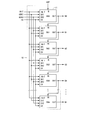
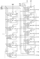
- FIG. 1 is a block diagram showing a configuration of a scanning line drive circuit 10 according to a first embodiment.
- the scanning line drive circuit 10 shown in FIG. 1 has a configuration in which (m + 1) unit circuits 11 are connected in multiple stages.
- the unit circuit 11 has an initialization terminal INIT, clock terminals CK1 and CK2, an input terminal IN, a control voltage terminal CV, and an output terminal OUT.
- a high level voltage VGH and a low level voltage VGL are supplied to the unit circuit 11 using wiring (not shown).
- FIG. 2 is a block diagram showing a configuration of an organic EL display device including a scanning line drive circuit 10.
- the organic EL display device 1 shown in FIG. 2 includes a display unit 2, a display control circuit 3, a scanning line drive circuit 10, a data line drive circuit 4, and a light emission control line drive circuit 5.
- the display unit 2 is formed on the organic EL panel 8 using a TFT.
- the scanning line drive circuit 10 and the light emission control line drive circuit 5 are integrally formed with the organic EL panel 8 by using a TFT.
- the data line drive circuit 4 is formed separately from the organic EL panel 8.
- all or a part of the data line drive circuit 4 may be formed integrally with the organic EL panel 8 by using a TFT, and all or a part of the light emission control line drive circuit 5 may be formed separately from the organic EL panel 8. You may.
- the display unit 2 includes (m + 1) scanning lines G0 to Gm, n data lines S1 to Sn, m light emitting control lines E1 to Em, and (m ⁇ n) pixel circuits 6. There is.
- the scanning lines G0 to Gm and the light emission control lines E1 to Em are arranged in parallel with each other.
- the data lines S1 to Sn are arranged parallel to each other so as to be orthogonal to the scanning lines G0 to Gm.
- the scanning lines G1 to Gm and the data lines S1 to Sn intersect at (m ⁇ n) points.
- the (m ⁇ n) pixel circuits 6 are arranged corresponding to the intersections of the scanning lines G1 to Gm and the data lines S1 to Sn.
- the pixel circuit 6 includes an organic EL element 7 as a light emitting element.
- the pixel circuit 6 in the i-th row and j-th column is connected to the scanning lines Gi-1, Gi, the data line Sj, and the light emission control line Ei.
- the pixel circuit 6 in the i-th row and j-th column may not be connected to the scanning line Gi-1, and the pixel circuit 6 in the i-th row and j-th column may be connected to another wiring.
- the display control circuit 3 outputs the control signal CS1 to the scanning line drive circuit 10, outputs the control signal CS2 and the video signal DS to the data line drive circuit 4, and controls the light emission control line drive circuit 5.
- the signal CS3 is output.
- the scanning line drive circuit 10 drives the scanning lines G0 to Gm based on the control signal CS1.
- the data line drive circuit 4 drives the data lines S1 to Sn based on the control signal CS2 and the video signal DS.
- the light emission control line drive circuit 5 drives the light emission control lines E1 to Em based on the control signal CS3.
- the scanning line drive circuit 10 sequentially selects one scanning line from the scanning lines G0 to Gm based on the control signal CS1, and applies a selected voltage (here, a low level voltage) to the selected scanning line. Apply and apply a non-selective voltage (here, high level voltage) to the remaining scan lines. As a result, in the i-th horizontal period, the pixel circuits 6 (n pixel circuits) in the i-th row are collectively selected. Based on the control signal CS2, the data line drive circuit 4 applies n voltages corresponding to the video signal DS to the data lines S1 to Sn, respectively. As a result, n voltages are written to each of the selected n pixel circuits 6. An amount of current corresponding to the voltage written in the pixel circuit 6 flows through the organic EL element 7, and the organic EL element 7 emits light with brightness corresponding to the amount of flowing current.
- a selected voltage here, a low level voltage
- a non-selective voltage here, high level voltage
- a light emitting period and a non-light emitting period are set for each line of the pixel circuit 6.
- the light emission control line drive circuit 5 applies a light emission voltage (here, a low level voltage) to the light emission control line Ei during the light emission period of the pixel circuit 6 on the i-th line, and emits light during the non-light emission period of the pixel circuit 6 on the i-th line.
- a non-emission voltage (here, a high level voltage) is applied to the control line Ei.
- (m + 1) unit circuits 11 are referred to as unit circuits in the 0th to mth stages in the order of connection.
- the display control circuit 3 outputs the initialization signal INIT, the gate clocks GCK1, GCK2, the gate start pulse GSP, and the control voltage CV as the control signal CS1 to the scanning line drive circuit 10.
- the initialization signal INIT is supplied to the initialization terminal INIT of the unit circuit 11 of each stage.
- the gate clock GCK1 is supplied to the clock terminal CK1 of the even-numbered unit circuit 11 and the clock terminal CK2 of the odd-numbered unit circuit 11.
- the gate clock GCK2 is supplied to the clock terminal CK2 of the even-numbered unit circuit 11 and the clock terminal CK1 of the odd-numbered unit circuit 11.
- the gate start pulse GSP is supplied to the input terminal IN of the 0th stage unit circuit 11.
- the control voltage CV is supplied to the control voltage terminal CV of the unit circuit 11 of each stage.
- the output terminal OUT of the unit circuit 11 of each stage is connected to the input terminal IN of the unit circuit 11 of the next stage and the corresponding scanning line among the scanning lines G0 to Gm.
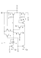
- FIG. 3 is a circuit diagram of the unit circuit 11. As shown in FIG. 3, the unit circuit 11 includes nine TFTs: M1 to M9, resistors R1, and two capacitors C1 and C2. TFTs: M1 to M9 are P-channel type TFTs.
- the resistor R1 is formed by using a P-type semiconductor (P-type polysilicon) in the same semiconductor layer as the semiconductor portion of the TFTs: M1 to M9.
- One end of the resistor R1 (right end in FIG. 3), the drain electrode of TFT: M1 and M3, the source electrode of TFT: M9, and the gate electrode of TFT: M4 and M7 are connected to the node n1.
- the source electrode of the TFT: M5 is connected to the other end of the resistor R1.
- One conduction electrode of TFT: M6 (the conduction electrode on the right side in FIG. 3) and the gate electrode of TFT: M8 are connected to the node n2.
- the source electrode of TFT: M2 and the drain electrode of TFT: M4 are connected to the other conduction electrode of TFT: M6.
- the gate electrode of the TFT: M9 is connected to the initialization terminal INIT.
- the gate electrode of the TFT: M5 is connected to the clock terminal CK1.
- the drain electrode of the TFT: M8 is connected to the clock terminal CK2.
- the gate electrodes of the TFTs: M1 and M2 are connected to the input terminal IN.
- the gate electrode of TFT: M3, the drain electrode of TFT: M7, and the source electrode of TFT: M8 are connected to the output terminal OUT.
- TFT: A high level voltage VGH is applied to the source electrodes of M1, M3, M4 and M7.
- a low level voltage VGL is applied to the drain electrodes of the TFTs: M2, M5 and M9 and the gate electrodes of the TFTs: M6.
- the capacitor C1 is provided between the gate electrode and the source electrode of the TFT: M7.
- the capacitor C2 is provided between the gate electrode and the source electrode of the TFT: M8.
- An upper electrode UE is formed on the resistor R1, and the upper electrode UE is connected to the control voltage terminal CV.
- the TFT: M1 functions as a first transistor in which a high level voltage VGH is applied to the source electrode and the drain electrode is connected to the node n1. One end of the resistor R1 is connected to the node n1.
- the TFT: M5 functions as a second transistor in which a low level voltage VGL is applied to the source electrode and the drain electrode is connected to the other end of the resistor R1.
- TFT: M1, M5 and resistor R1 form a ratio circuit.
- the TFT: M7 functions as an output transistor in which the gate electrode is connected to the node n1 and the drain electrode is connected to the output terminal OUT.
- the resistor R1 is formed in the same semiconductor layer as the semiconductor portion of the first and second transistors.
- the initialization signal INIT is at a low level during the initialization period of the scanning line drive circuit 10, and is at a high level at other times.
- the TFT: M9 is turned on and the voltage at node n1 is initialized to a low level.
- the TFT: M9 is turned off except during the initialization period. Since the low level voltage VGL is fixedly applied to the gate electrode of the TFT: M6, the TFT: M6 is always on. Therefore, the TFTs: M6 and M9 do not affect the normal operation of the unit circuit 11.
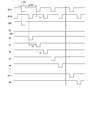
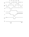
- FIG. 4 is a timing chart of the scanning line drive circuit 10.
- the gate clocks GCK1 and GCK2 are clock signals having a period of two horizontal periods (2H).
- the length of the high level period of the gate clocks GCK1 and GCK2 is 3/2 horizontal period, and the length of the low level period is 1/2 horizontal period.
- the gate clock GCK2 is delayed by one horizontal period from the gate clock GCK1.
- the gate start pulse GSP becomes a low level once in one frame period when the gate clock GCK1 is at a low level, and becomes a high level at other times.
- the control voltage CV is a fixed negative voltage slightly higher than the low level voltage VGL.
- the control voltage CV is applied to the upper electrode UE in the unit circuit 11 of each stage.
- FIG. 5 is a timing chart of the unit circuit 11.
- the intervals between the times t1 to t6 are all 1/2 horizontal periods.
- the voltage of the upper electrode UE is a fixed negative voltage slightly higher than the low level voltage VGL.
- a signal input or output via a certain terminal is referred to by the same name as that terminal.
- a signal input via the clock terminal CK1 is called a clock signal CK1.
- the clock signals CK1 and CK2, the input signal IN, the voltage of the node n2, and the output signal OUT are at a high level, and the voltage of the node n1 is at a low level. Therefore, the TFTs: M1 to M3, M5 and M8 are in the off state, and the TFTs: M4 and M7 are in the on state.
- the clock signal CK1 and the input signal IN change to a low level.
- the TFTs: M1, M2, and M5 are turned on.
- a high level voltage VGH is applied to the node n1 via the TFT: M1
- a low level voltage VGL is applied to the node n1 via the TFT: M5 and the resistor R1.
- the resistance value of the resistor R1 is sufficiently larger than the resistance value when the TFT: M1 is on. Therefore, the voltage of the node n1 changes to a high level after the time t1, and the TFTs: M4 and M7 are turned off.
- a low level voltage VGL is applied to the node n2 via the TFT: M2.
- the TFT: M4 when the TFT: M4 is turned off, the voltage of the node n2 changes to a low level, and the TFT: M8 is turned on accordingly.
- the clock signal CK1 and the input signal IN change to a high level.
- the TFTs: M1, M2, and M5 are turned off.
- the clock signal CK2 changes to a low level.
- the TFT: M8 since the TFT: M8 is in the ON state, the output signal OUT changes to a low level.
- a capacitor C2 is provided between the gate electrode and the source electrode of the TFT: M8. Therefore, while the output signal OUT is at a low level, the voltage of the node n2 becomes a level lower than the normal low level. Therefore, the low level voltage of the output signal OUT becomes the same level as the low level voltage of the clock signal CK2 without increasing by the threshold voltage of the TFT: M8.
- the TFT: M3 When the output signal OUT changes to a low level, the TFT: M3 is turned on. TFT: M3 applies a high level voltage VGH to node n1 while the output signal OUT is low level.
- the clock signal CK2 changes to a high level.
- the output signal OUT changes to a high level.
- the voltage of the node n2 changes to a normal low level, and the TFT: M3 is turned off.
- the clock signal CK1 changes to a low level.
- the TFTs: M1 and M2 are turned on. Since the low level voltage VGL is applied to the node n1 via the TFT: M5 and the resistor R1, the voltage of the node n1 changes to the low level.
- the TFTs: M4 and M7 are turned on, and the voltage of the node n2 changes to a high level.
- the clock signal CK1 changes to a high level, and the TFT: M5 is turned off accordingly.
- the unit circuit 11 performs a set operation to raise the voltage of the node n1 to a high level when the input signal IN and the clock signal CK1 are at a low level, and the input signal IN is at a high level and the clock signal CK1 is at a low level.
- a reset operation is performed to bring the voltage of the node n1 to a low level.
- the voltage of the node n1 changes to a high level after the time t1 when the input signal IN and the clock signal CK1 change to a low level, and the time t5 when the clock signal CK1 changes to a low level while the input signal IN is high level. After that, it changes to a low level.
- the voltage of node n2 becomes high level when the voltage of node n1 is low level, and becomes low level at other times.
- the output signal OUT becomes a low level for 1/2 horizontal period, which is delayed by 1 horizontal period from the input signal IN.
- the output terminals OUT of the unit circuit 11 in the 0th to mth stages are connected to the scanning lines G0 to Gm, respectively. Therefore, as shown in FIG. 4, the voltage of the scanning line G0 becomes low level by 1/2 horizontal period later than the voltage of the gate start pulse GSP by 1 horizontal period.
- the voltage of the scanning line Gi becomes a low level for 1/2 horizontal period, which is delayed by one horizontal period from the voltage of the scanning line Gi-1. Therefore, the voltage of the scanning lines G0 to Gm is delayed by one horizontal period in order and becomes low level for 1/2 horizontal period.
- FIG. 6 is a layout diagram showing a part of the unit circuit 11.
- FIG. 6 shows the layout patterns of the TFTs: M1, M5, the resistor R1, and the upper electrode UE.
- the wiring layer on which the semiconductor layers of TFT: M1 to M9 are formed is the semiconductor layer
- the wiring layer on which the gate electrodes of TFT: M1 to M9 are formed is the gate wiring layer
- the wiring layer on which the wiring connected to is formed is referred to as a source wiring layer
- the wiring layer on which the anode electrode of the organic EL element 7 is formed is referred to as an anode electrode layer.
- the gate wiring layer is above the semiconductor layer
- the source wiring layer is above the gate wiring layer
- the anode electrode layer is above the source wiring layer.
- a region with a downward-sloping diagonal line shows a pattern of a semiconductor layer
- a region with a crosshatch shows a pattern of a gate wiring layer
- a region with a downward-sloping diagonal line shows a pattern of a source wiring layer.
- the crossed rectangles indicate contact holes that electrically connect the semiconductor layer and the source wiring layer.
- the patterns of the layers other than the semiconductor layer, the gate wiring layer, and the source wiring layer are omitted, and are applied to the pattern near the pattern. The name of the voltage or the terminal to which the pattern is connected is described.
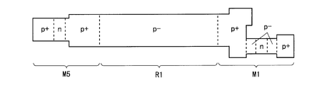
- FIG. 7 is a diagram showing a pattern of semiconductor layers included in the layout diagram shown in FIG. As shown in FIG. 7, a p + region, an n region, and a p + region are formed at the position of the TFT: M5. A p- region is formed at the position of the resistor R1. At the position of TFT: M1, a p + region, a p- region, an n region, a p- region, and a p + region are formed.
- the p + region is a region containing a relatively large amount of P-type semiconductor
- the p- region is a region containing a relatively small amount of P-type semiconductor.
- the n region functions as a channel region.
- FIG. 8 is a cross-sectional view taken along the line AA'of FIG.
- the upper electrode UE is formed on the resistor R1.
- the upper electrode UE is formed in the source wiring layer.
- the resistance value of the resistor R1 is, for example, 0.1 M ⁇ or more and 7 M ⁇ or less.
- An insulating film 104 and interlayer insulating films 111 and 112 are interposed between the resistor R1 and the upper electrode UE.
- the total thickness of these insulating films is, for example, 200 nm or more and 1 ⁇ m or less.
- FIGS. 9A to 9M are diagrams showing a manufacturing process of the organic EL panel 8 including the scanning line drive circuit 10.
- the backcoat 102 is deposited on the polyimide substrate 101, the amorphous silicon 103 is deposited at the position where the pattern of the semiconductor layer is formed, and the insulating film 104 is formed using silicon dioxide (SiO 2) (FIG. 9A).
- the amorphous silicon 103 on the substrate is sequentially irradiated with the excimer laser LS to modify the amorphous silicon 103 into polysilicon 105 (FIG. 9B).
- the gate electrode 106 of the TFT is formed using molybdenum at the position where the TFT is formed (FIG. 9C).
- boron is injected into the polysilicon 105 on the substrate by irradiating it with boron ions.
- the portion of the polysilicon 105 on the substrate that is not covered by the gate electrode 106 becomes the p-region 107, and the portion that is covered by the gate electrode 106 becomes the n region 108 (FIG. 9D).
- the resist 109 is applied to the position Pos_R1 or the like where the resistor R1 is formed, and the boron ion is further irradiated.
- the portion of the p-region 107 that is not covered by the resist 109 changes to the p + region 110 (FIG. 9E).
- the resist 109 is peeled off (FIG. 9F).
- the p-region 107 at position Pos_R1 functions as a resistor R1.
- the interlayer insulating film 111 is formed using silicon nitride (SiN x ), and the interlayer insulating film 112 is formed using silicon nitride and silicon oxide (SiO x) (FIG. 9G).
- a contact hole 113 penetrating the insulating film 104 and the interlayer insulating films 111 and 112 is opened at a position where the drain electrode and the source electrode of the TFT are formed (FIG. 9H).
- various wirings are formed using titanium, aluminum, and titanium at predetermined positions on the substrate (Fig. 9I).
- the wiring 114 for supplying the high level voltage VGH, the wiring 115 for supplying the low level voltage VGL, the wiring 116 for connecting the electrodes of the TFT, and the like are formed.
- the contact hole 113 is filled with the above metal material to form the drain electrode 117 of the TFT and the source electrode 118.
- the drain electrode 117 and the source electrode 118 electrically connect the p + region 110 and the wirings 114 to 116.
- An upper electrode UE is formed on the resistor R1 so as to cover the resistor R1.
- a flattening film 119 is formed using polyimide (Fig. 9J).
- a through hole is opened at a predetermined position on the substrate, and titanium, aluminum, and titanium are used to form the wiring 120 at the predetermined position on the substrate (FIG. 9K).
- the flattening film 121 is formed using polyimide, and the anode electrode 122 is formed at a predetermined position on the substrate using silver (FIG. 9L).
- the bank 123 is formed by using polyimide at a predetermined position on the substrate (FIG. 9M).
- the substrate shown in FIG. 8 can be obtained.
- the organic EL layer, the cathode electrode, and the sealing film in this order on the substrate shown in FIG. 8 the organic EL panel 8 including the scanning line drive circuit 10 can be manufactured.
- the above material is an example, and a material other than the above may be used.
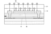
- FIG. 10 is a diagram for explaining a problem of a conventional scanning line drive circuit.
- FIG. 11 is a diagram for explaining the effect of the scanning line drive circuit 10. 10 and 11 show a cross section in the vicinity of a resistor in the unit circuit of the scanning line drive circuit. The same reference numerals are given to the corresponding components in order to facilitate the comparison of the drawings.
- the upper electrode is not formed on the resistor R9. Therefore, when the charging EC is captured by the insulating films (flattening films 119 and 112) formed on the resistor R9 and their interfaces, the electric lines of force emitted from the charged EC are the resistors formed in the semiconductor layer. Enter R9. Therefore, the carriers induced in the resistor R9 fluctuate, and the resistance value of the resistor R9 fluctuates. The resistance value of the resistor R9 increases with the passage of time. In the conventional scanning line drive circuit, when the resistance value of the resistor R9 becomes large, a reset failure occurs. Therefore, in the conventional organic EL display device provided with the scanning line drive circuit, display defects such as flickering occur on the display screen.
- the upper electrode UE is formed on the resistor R1. Therefore, when the charged EC is captured by the insulating film formed on the resistor R1 or its interface, the electric lines of force emitted from the charged EC do not enter the resistor R1 due to the action of the upper electrode UE. Therefore, the carriers induced in the resistor R1 do not fluctuate, and the resistance value of the resistor R1 does not fluctuate. Therefore, according to the scanning line drive circuit 10, it is possible to prevent a reset failure due to a variation in the characteristics of the resistor R1. Further, according to the organic EL display device 1 provided with the scanning line drive circuit 10, it is possible to prevent display defects such as flickering from occurring on the display screen.
- the resistor R1 is formed by using a P-type semiconductor, and a fixed negative voltage (control voltage CV) is applied to the upper electrode UE.
- a fixed negative voltage control voltage CV
- the resistance value of the resistor R1 becomes smaller.
- the upper electrode UE since the upper electrode UE is formed in the source wiring layer, it does not contain an organic film that easily contains water or electric charge between the resistor R1 and the upper electrode UE. Therefore, the scanning line drive circuit 10 can be operated more stably.
- the scanning line drive circuit 10 has a configuration in which a plurality of unit circuits 11 are connected in multiple stages, and is integrally formed with a display panel (organic EL panel 8).
- a first level voltage high level voltage VGH
- VGH high level voltage
- drain electrode the other conduction electrode
- a second level voltage low level voltage VGL
- TFT: M1 one transistor
- R1 resistor
- the resistor R1 is formed in the same semiconductor layer as the semiconductor portion of the first and second transistors, and the upper electrode UE is formed on the resistor R1.
- the scanning line drive circuit 10 by forming the upper electrode UE on the resistor R1, the resistor is prevented from being affected by the electric charge captured by the insulating film or the like formed on the resistor R1.
- the characteristic fluctuation of the resistor R1 can be reduced. Therefore, it is possible to prevent the scanning line drive circuit 10 from malfunctioning due to the characteristic variation of the resistor R1.
- the resistor R1 is formed by using a P-type semiconductor (P-type polysilicon). Therefore, the scanning line drive circuit 10 including the unit circuit 11 including the resistor R1 can be integrally formed with the display panel.
- the upper electrode UE is connected to a wiring layer above the control electrodes (gate electrodes) of the first and second transistors, specifically, conduction electrodes (source electrode and drain electrode) of the first and second transistors. It is formed in the same wiring layer (source wiring layer) as the wirings 114 to 116. Therefore, since the organic film that easily contains water or electric charge is not contained between the resistor R1 and the upper electrode UE, the scanning line drive circuit 10 can be operated more stably.
- the resistance value of the resistor R1 is preferably 0.1 M ⁇ or more and 7 M ⁇ or less.
- the unit circuit 11 can perform the set operation and the reset operation at high speed.
- an insulating film (interlayer insulating film 111, 112) having a thickness of 200 nm or more and 1 ⁇ m or less is interposed between the resistor R1 and the upper electrode UE. By providing the insulating film having such a thickness, the resistor R1 and the upper electrode UE can be arranged at a suitable distance.
- the output signal OUT of the unit circuit in the previous stage is given to the control electrode (gate electrode) of the first transistor, and the clock signal (gate clock GCK1 or GCK2) is given to the control electrode of the second transistor.
- the first and second transistors can be turned on at appropriate timings, and the scanning line drive circuit 10 can be operated correctly.
- a fixed negative voltage (control voltage CV) is applied to the upper electrode UE, and the negative voltage is, for example, -10V or more and -5V or less.
- the resistance value of the resistor R1 becomes smaller. Therefore, the unit circuit 11 can easily perform the reset operation.
- FIG. 12 is a cross-sectional view of a unit circuit of a scanning line drive circuit according to a modified example of the present embodiment.
- the upper electrode UE is formed not in the source wiring layer but in the same wiring layer as the anode electrode 122 of the organic EL element 7.
- the interlayer insulating films 111 and 112 and the flattening films 119 and 121 are interposed between the resistor R1 and the upper electrode UE as insulating films.
- the scanning line driving circuit according to the modified example it is possible to prevent the scanning line driving circuit from malfunctioning due to the characteristic variation of the resistor R1 as in the scanning line driving circuit 10 according to the first embodiment.
- FIG. 13 is a block diagram showing a configuration of a scanning line drive circuit according to a second embodiment.
- the scanning line drive circuit 20 shown in FIG. 13 has a configuration in which (m + 1) unit circuits 21 are connected in multiple stages.
- the unit circuit 21 has an initialization terminal INIT, clock terminals CK1 and CK2, an input terminal IN, and an output terminal OUT.
- the differences from the first embodiment will be described.
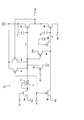
- FIG. 14 is a circuit diagram of the unit circuit 21.
- the low level voltage VGL is fixedly applied to the upper electrode UE formed on the resistor R1.
- FIG. 15 is a timing chart of the unit circuit 21. As shown in FIG. 15, the voltage of the upper electrode UE is always equal to the low level voltage VGL.
- a fixed negative voltage equal to the low level voltage VGL supplied to the unit circuit 21 is applied to the upper electrode UE. According to the scanning line driving circuit 20, it is possible to prevent the scanning line driving circuit 10 from malfunctioning due to the characteristic fluctuation of the resistor R1 as in the first embodiment without providing the wiring for supplying the control voltage CV. Can be done.
- the scanning line driving circuit according to the third embodiment is obtained by replacing the unit circuit 21 with another unit circuit in the scanning line driving circuit 20 (FIG. 13) according to the second embodiment.
- the differences from the second embodiment will be described.
- FIG. 16 is a circuit diagram of a unit circuit of the scanning line drive circuit according to the present embodiment.
- the upper electrode UE formed on the resistor R1 is connected to the node n1.
- the node n1 is connected to the drain electrode of the TFT: M1, one end of the resistor R1 (the right end in FIG. 16), the gate electrode of the TFT: M7, and the like.
- the voltage of the upper electrode UE is equal to the voltage of node n1.
- FIG. 17 is a timing chart of the unit circuit 31.
- the voltage of the upper electrode UE changes in the same manner as the voltage of the node n1. More specifically, the voltage of the upper electrode UE changes to a high level after the time t1 when the input signal IN and the clock signal CK1 change to a low level, and the clock signal CK1 is low while the input signal IN is at a high level. It changes to a low level after the time t5 when it changes to a level.
- the time t1 is the time when the unit circuit 31 starts the set operation
- the time t5 is the time when the unit circuit 31 starts the reset operation.
- the resistance value of the resistor R1 becomes small, and the unit circuit 11 can easily perform the reset operation. However, if the resistance value of the resistor R1 is reduced, it becomes difficult for the unit circuit 11 to perform the set operation.
- the resistance value of the resistor R1 is preferably small for the reset operation and large for the set operation.
- the upper electrode UE is connected to the node n1.
- the voltage of the upper electrode UE rises with the voltage of the node n1 to a high level. Therefore, while the unit circuit 31 is performing the set operation, a positive voltage is applied to the upper electrode UE, and the resistance value of the resistor R1 becomes large. Therefore, the unit circuit 31 can easily perform the set operation.
- the unit circuit 31 starts the reset operation at time t5
- the voltage of the upper electrode UE drops together with the voltage of the node n1 and becomes a low level. Therefore, while the unit circuit 31 is performing the reset operation, a negative voltage is applied to the upper electrode UE, and the resistance value of the resistor R1 becomes smaller. Therefore, the unit circuit 31 can easily perform the reset operation.
- the upper electrode UE is connected to the other conduction electrode (TFT: drain electrode of M1) of the first transistor and the first node (node n1) connected to one end of the resistor R1. Has been done.
- TFT drain electrode of M1
- node n1 the first node connected to one end of the resistor R1.
- a positive voltage is applied to the upper electrode UE, and when the unit circuit 31 performs the reset operation, a negative voltage is applied to the upper electrode UE, so that the unit circuit 31 is set with the reset operation. Both operations can be easily performed.
- the scan line drive circuit according to the fourth embodiment is obtained by replacing the unit circuit 21 with another unit circuit in the scan line drive circuit 20 (FIG. 13) according to the second embodiment.
- the differences from the third embodiment will be described.
- FIG. 18 is a circuit diagram of a unit circuit of the scanning line drive circuit according to the present embodiment.
- the upper electrode UE formed on the resistor R1 is connected to the other end of the resistor R1 (the left end in FIG. 18).
- the other end of the resistor R1 is connected to the source electrode of TFT: M5.
- the timing chart of the scanning line drive circuit according to the present embodiment is substantially the same as the timing chart shown in FIG.
- the unit circuit 41 in which the upper electrode UE is connected to the other end of the resistor R1 operates in the same manner as the unit circuit 31 according to the third embodiment in which the upper electrode UE is connected to the node n1.
- the upper electrode UE is connected to the other end of the resistor R1 connected to the other conduction electrode (TFT: source electrode of M5) of the second transistor.
- TFT source electrode of M5
- the unit circuit 41 can easily perform both a reset operation and a set operation.
- FIG. 19 is a block diagram showing a configuration of a scanning line drive circuit according to a fifth embodiment.
- the scanning line drive circuit 50 shown in FIG. 19 has a configuration in which (m + 1) unit circuits 11 are connected in multiple stages.
- (m + 1) unit circuits 11 are connected in multiple stages.
- the differences from the first embodiment will be described.
- the scanning line driving circuit 50 and the light emitting control line driving circuit 5 are arranged on the same side of the display unit 2.
- the display control circuit 3 outputs the initialization signal INIT, the gate clocks GCK1, GCK2, and the gate start pulse GSP as the control signal CS1 to the scanning line drive circuit 50. These control signals are supplied to the corresponding terminals of the unit circuit 11 as in the first embodiment.
- the output terminal OUT of the unit circuit 11 of each stage is connected to the input terminal IN of the unit circuit 11 of the next stage and the corresponding scanning line among the scanning lines G0 to Gm, as in the first embodiment.
- the light emission control line drive circuit 5 has a configuration in which (m + 1) unit circuits 9 are connected in multiple stages.
- the unit circuit 9 has an initialization terminal INIT, clock terminals CK1 and CK2, an input terminal IN, and an output terminal OUT.
- the (m + 1) unit circuits 9 are referred to as unit circuits in the 0th to mth stages in the order of connection, and the wiring to which the output terminals OUT of the 0th stage unit circuits 9 are connected is referred to as E0.
- the display control circuit 3 outputs the initialization signal INIT, the emission clocks EMCK1, EMCK2, and the emission start pulse EMSP as the control signal CS3 to the light emission control line drive circuit 5. These control signals are supplied to the corresponding terminals of the unit circuit 9, as shown in FIG.
- the output terminal OUT of the unit circuit 9 of each stage is connected to the input terminal IN of the unit circuit 9 of the next stage and the corresponding wiring of the wiring E0 and the light emission control lines E1 to Em.
- the control voltage terminals CVs of the unit circuits 11 in the 0th to mth stages are connected to the output terminals OUT of the unit circuits 9 in the 0th to mth stages, respectively. Therefore, the upper electrode UE in the 0th-stage unit circuit 11 is connected to the wiring E0, and the upper electrode UE in the i-th stage unit circuit 11 is connected to the light emission control line Ei.
- FIG. 20 is a timing chart of the scanning line drive circuit 50.
- n1_0 to 4 indicate the voltage of the node n1 of the unit circuit 11 in the 0th to 4th stages, respectively.
- the voltages of the gate start pulse GSP, the gate clocks GCK1 and GCK2, and the scanning lines G0 to Gm change in the same manner as in the timing chart shown in FIG.
- Emission clocks EMCK1 and EMCK2 are clock signals having a period of 2 horizontal periods.
- the length of the high level period of the emission clocks EMCK1 and EMCK2 is 3/2 horizontal period, and the length of the low level period is 1/2 horizontal period.
- the emission clock EMCK1 lags the gate clock GCK1 by a 3/4 horizontal period.
- the emission clock EMCK2 lags the emission clock EMCK1 by one horizontal period.
- the emission start pulse EMSP becomes a high level for 3 horizontal periods from a time 9/4 horizontal period earlier than the time when the gate start pulse GSP changes to a low level.
- the unit circuit 9 changes the output signal OUT to a high level when the clock signal CK1 changes to a low level while the input signal IN is at a high level, and the clock signal CK2 changes to a high level while the input signal IN is at a low level.
- the output signal OUT is changed to the low level when it changes to the low level. Therefore, the output signal OUT becomes a high level for 3 horizontal periods, which is delayed by 1 horizontal period from the input signal IN. Therefore, the voltages of the wiring E0 and the light emission control lines E1 to Em become high levels over the three horizontal periods with a delay of one horizontal period in order.
- the voltage of the upper electrode UE in the unit circuit 11 in the 0th to mth stages is delayed by one horizontal period in order to reach a high level over three horizontal periods.
- FIG. 21 is a timing chart of the unit circuit 11 according to the present embodiment.
- the voltage of the upper electrode UE changes to a high level at time t11 and changes to a low level at time t12.
- the time t11 is a time 5/4 horizontal period earlier than the time t1 at which the input signal IN and the clock signal CK1 change to a low level.
- the time t12 is a time that is 1/4 horizontal period earlier than the time t5 in which the clock signal CK1 changes to the low level while the input signal IN is at a high level. In this way, a positive voltage and a negative voltage are switched and applied to the upper electrode UE.
- the voltage of the upper electrode UE changes to a high level at a time t11 before the time t1 when the voltage of the node n1 starts to change from a low level to a high level, and the voltage of the node n1 starts to change from a high level to a low level. It changes to a low level at time t12 before time t5. Therefore, the voltage of the upper electrode UE is high level when the voltage of the node n1 changes from low level to high level, and is low level when the voltage of node n1 changes from high level to low level.
- the voltage of the upper electrode UE is already at a high level before the unit circuit 11 starts the set operation at time t1. Therefore, while the unit circuit 11 is performing the set operation, a positive voltage is applied to the upper electrode UE, and the resistance value of the resistor R1 becomes large. Therefore, the unit circuit 11 can easily perform the set operation.
- the voltage of the upper electrode UE is already at a low level before the unit circuit 11 starts the reset operation at time t5. Therefore, while the unit circuit 11 is performing the reset operation, a negative voltage is applied to the upper electrode UE, and the resistance value of the resistor R1 becomes smaller. Therefore, the unit circuit 11 can easily perform the reset operation.
- a plurality of light emission control lines E1 to Em are formed on the display panel (organic EL panel 8), and the upper electrode UE has a plurality of light emission controls. It is connected to the corresponding light emission control line among the lines E1 to Em.
- a positive voltage (high level voltage) and a negative voltage (low level voltage) are switched and applied to the upper electrode UE, and the voltage of the first node (node n1) is applied from the first level (high level) to the second level (low level). ), A negative voltage is applied to the upper electrode UE.
- a positive voltage is applied to the upper electrode UE.
- the scanning line driving circuit 50 it is possible to prevent the scanning line driving circuit 50 from malfunctioning due to the characteristic fluctuation of the resistor R1 as in the first embodiment. Further, by applying a positive voltage to the upper electrode UE before the unit circuit 11 starts the set operation and applying a negative voltage to the upper electrode UE before the unit circuit 11 starts the reset operation, the unit circuit 11 can easily perform both a reset operation and a set operation. Further, by connecting the upper electrode UE to the light emission control line formed on the display panel (organic EL panel 8), a positive voltage and a negative voltage can be switched and applied to the upper electrode UE with a simple configuration.
- FIG. 22 is a block diagram showing a configuration of a scanning line drive circuit according to a sixth embodiment.
- the scanning line drive circuit 60 shown in FIG. 22 has a configuration in which (m + 1) unit circuits 11 are connected in multiple stages.
- (m + 1) unit circuits 11 are connected in multiple stages.
- the configuration of the light emission control line drive circuit 5 shown in FIG. 22 is the same as that of the fifth embodiment.
- the display control circuit 3 outputs the initialization signal INIT, the emission clocks EMCK1, EMCK2, and the emission start pulse EMSP as the control signal CS3 to the light emission control line drive circuit 5.
- the emission clock EMCK2 output from the display control circuit 3 is supplied to the control voltage terminal CV of the even-numbered unit circuit 11 of the scanning line drive circuit 60.
- the emission clock EMCK1 output from the display control circuit 3 is supplied to the control voltage terminal CV of the odd-numbered unit circuit 11 of the scanning line drive circuit 60. Therefore, the voltage of the upper electrode UE in the even-numbered unit circuit 11 changes in the same manner as the emission clock EMCK2, and the voltage of the upper electrode UE in the odd-numbered unit circuit 11 changes in the same manner as the emission clock EMCK1.
- the timing chart of the scanning line drive circuit 60 according to the present embodiment is the same as the timing chart shown in FIG.
- FIG. 23 is a timing chart of the unit circuit 11 according to the present embodiment.
- the voltage of the upper electrode UE changes in the same manner as either of the emission clocks EMCK1 and EMCK2.
- the voltage of the upper electrode UE is low level in the period from time t21 to time t22 and in the period from time t23 to time t24, and is high level in other cases.
- the time t21 is a time that is 1/4 horizontal period earlier than the time t1 at which the input signal IN and the clock signal CK1 change to a low level.
- Time t22 is a time that is 1/4 horizontal period later than time t1.
- the time t23 is a time 1/4 horizontal period earlier than the time t5 in which the clock signal CK1 changes to the low level while the input signal IN is at a high level.
- Time t24 is a time that is 1/4 horizontal period later than time t5.
- the voltage of the upper electrode UE changes to a low level at a time t23 before the time t5 when the voltage of the node n1 starts to change from a high level to a low level. Therefore, when the voltage of the node n1 changes from high level to low level, the voltage of the upper electrode UE is low level.
- the voltage of the upper electrode UE is already at a low level before the unit circuit 11 starts the reset operation at time t5. Therefore, while the unit circuit 11 is performing the reset operation, a negative voltage is applied to the upper electrode UE, and the resistance value of the resistor R1 becomes smaller. Therefore, the unit circuit 11 can easily perform the reset operation.
- the light emission control line drive circuit 5 does not necessarily have to be integrally formed with the organic EL panel 8. Even when the light emission control line drive circuit 5 is formed separately from the organic EL panel 8, two wires propagating the emission clocks EMCK1 and EMCK2 are formed on the organic EL panel 8 to control the unit circuit 11 of the even-stage.
- the voltage terminal CV may be connected to the wiring propagating the emission clock EMCK2, and the control voltage terminal CV of the odd-stage unit circuit 11 may be connected to the wiring propagating the emission clock EMCK1.
- the display panel (organic EL panel 8) has a plurality of wirings for propagating a plurality of clock signals (emission clocks EMCK1 and EMCK2) for light emission control. It is formed and the upper electrode UE is connected to the corresponding wiring among the plurality of wirings.
- the scanning line driving circuit 60 it is possible to prevent the scanning line driving circuit 60 from malfunctioning due to the characteristic fluctuation of the resistor R1 as in the first embodiment. Further, by applying a negative voltage to the upper electrode UE before the unit circuit 11 starts the reset operation, the unit circuit 11 can easily perform the reset operation. Further, by connecting the upper electrode UE to the wiring for propagating the clock signal for light emission control formed on the display panel (organic EL panel 8), the upper electrode UE can be switched between positive voltage and negative voltage with a simple configuration. Can be applied.
- the unit circuit of the scanning line drive circuit according to the modification includes the first transistor, the resistor, the second transistor, and the output transistor connected in the above embodiment, and is above the resistor formed in the semiconductor layer. It may have other configurations as long as the electrodes are formed.
- the display device provided with the scanning line drive circuit according to the modified example may include any pixel circuit.
- the voltage control circuit may switch between positive voltage and negative voltage and apply the voltage to the upper electrode UE.
- the voltage control circuit is configured to apply a negative voltage to the upper electrode UE when the voltage of the first node (node n1) changes from the first level (high level) to the second level (low level). .. More preferably, the voltage control circuit is configured to apply a positive voltage to the upper electrode UE when the voltage of the first node changes from the second level to the first level. Even when such a voltage control circuit is used, the unit circuit of the scanning line drive circuit can easily perform a reset operation (or both a reset operation and a set operation).
- an organic EL display device having a pixel circuit including an organic EL element organic light emitting diode
- An inorganic EL display device having a pixel circuit including a A display device may be configured. Further, the characteristics of the display device described above may be arbitrarily combined as long as the characteristics are not contrary to the properties thereof to form a display device having the characteristics of the above-described embodiment and the modified example.
Landscapes
- Engineering & Computer Science (AREA)
- Physics & Mathematics (AREA)
- General Physics & Mathematics (AREA)
- Theoretical Computer Science (AREA)
- Computer Hardware Design (AREA)
- Control Of Indicators Other Than Cathode Ray Tubes (AREA)
- Devices For Indicating Variable Information By Combining Individual Elements (AREA)
- Electroluminescent Light Sources (AREA)
- Control Of El Displays (AREA)
- Shift Register Type Memory (AREA)
Priority Applications (4)
| Application Number | Priority Date | Filing Date | Title |
|---|---|---|---|
| JP2022504765A JP7354407B2 (ja) | 2020-03-02 | 2020-03-02 | 走査線駆動回路およびこれを備えた表示装置 |
| US17/908,003 US11735120B2 (en) | 2020-03-02 | 2020-03-02 | Scanning-line driving circuit and display device provided with same |
| CN202080097740.5A CN115191013B (zh) | 2020-03-02 | 2020-03-02 | 扫描线驱动电路和具备其的显示装置 |
| PCT/JP2020/008640 WO2021176504A1 (ja) | 2020-03-02 | 2020-03-02 | 走査線駆動回路およびこれを備えた表示装置 |
Applications Claiming Priority (1)
| Application Number | Priority Date | Filing Date | Title |
|---|---|---|---|
| PCT/JP2020/008640 WO2021176504A1 (ja) | 2020-03-02 | 2020-03-02 | 走査線駆動回路およびこれを備えた表示装置 |
Publications (1)
| Publication Number | Publication Date |
|---|---|
| WO2021176504A1 true WO2021176504A1 (ja) | 2021-09-10 |
Family
ID=77613936
Family Applications (1)
| Application Number | Title | Priority Date | Filing Date |
|---|---|---|---|
| PCT/JP2020/008640 Ceased WO2021176504A1 (ja) | 2020-03-02 | 2020-03-02 | 走査線駆動回路およびこれを備えた表示装置 |
Country Status (4)
| Country | Link |
|---|---|
| US (1) | US11735120B2 (https=) |
| JP (1) | JP7354407B2 (https=) |
| CN (1) | CN115191013B (https=) |
| WO (1) | WO2021176504A1 (https=) |
Cited By (1)
| Publication number | Priority date | Publication date | Assignee | Title |
|---|---|---|---|---|
| WO2023084744A1 (ja) * | 2021-11-12 | 2023-05-19 | シャープディスプレイテクノロジー株式会社 | 表示装置 |
Citations (5)
| Publication number | Priority date | Publication date | Assignee | Title |
|---|---|---|---|---|
| JP2006311579A (ja) * | 1997-02-26 | 2006-11-09 | Toshiba Corp | 検知回路 |
| JP2010277652A (ja) * | 2009-05-29 | 2010-12-09 | Mitsubishi Electric Corp | シフトレジスタ回路、シフトレジスタ回路の設計方法及び半導体装置 |
| WO2012029799A1 (ja) * | 2010-09-02 | 2012-03-08 | シャープ株式会社 | シフトレジスタ及び表示装置 |
| JP2014056256A (ja) * | 2013-11-05 | 2014-03-27 | Mitsubishi Electric Corp | 画像表示装置 |
| WO2015012207A1 (ja) * | 2013-07-25 | 2015-01-29 | シャープ株式会社 | シフトレジスタ及び表示装置 |
Family Cites Families (9)
| Publication number | Priority date | Publication date | Assignee | Title |
|---|---|---|---|---|
| US5030852A (en) * | 1989-05-08 | 1991-07-09 | Mitsubishi Denki Kabushiki Kaisha | Quasicomplementary MESFET logic circuit with increased noise imunity |
| JP2002123229A (ja) * | 2000-10-18 | 2002-04-26 | Matsushita Electric Ind Co Ltd | 表示パネル走査線ドライバ |
| US9711238B2 (en) * | 2011-12-16 | 2017-07-18 | Sharp Kabushiki Kaisha | Shift register, scan signal line driver circuit, display panel and display device |
| TWI509593B (zh) * | 2013-12-20 | 2015-11-21 | Au Optronics Corp | 移位暫存器 |
| WO2016175117A1 (ja) | 2015-04-28 | 2016-11-03 | シャープ株式会社 | シフトレジスタ |
| US20180149911A1 (en) * | 2015-05-25 | 2018-05-31 | Sharp Kabushiki Kaisha | Drive circuit of display device |
| CN106098003B (zh) * | 2016-08-08 | 2019-01-22 | 武汉华星光电技术有限公司 | Goa电路 |
| CN107168587B (zh) * | 2017-07-13 | 2019-08-27 | 京东方科技集团股份有限公司 | 一种压阻检测基板、显示面板及显示装置 |
| WO2019123089A1 (ja) * | 2017-12-22 | 2019-06-27 | 株式会社半導体エネルギー研究所 | 表示装置、半導体装置、及び電子機器 |
-
2020
- 2020-03-02 JP JP2022504765A patent/JP7354407B2/ja active Active
- 2020-03-02 CN CN202080097740.5A patent/CN115191013B/zh active Active
- 2020-03-02 US US17/908,003 patent/US11735120B2/en active Active
- 2020-03-02 WO PCT/JP2020/008640 patent/WO2021176504A1/ja not_active Ceased
Patent Citations (5)
| Publication number | Priority date | Publication date | Assignee | Title |
|---|---|---|---|---|
| JP2006311579A (ja) * | 1997-02-26 | 2006-11-09 | Toshiba Corp | 検知回路 |
| JP2010277652A (ja) * | 2009-05-29 | 2010-12-09 | Mitsubishi Electric Corp | シフトレジスタ回路、シフトレジスタ回路の設計方法及び半導体装置 |
| WO2012029799A1 (ja) * | 2010-09-02 | 2012-03-08 | シャープ株式会社 | シフトレジスタ及び表示装置 |
| WO2015012207A1 (ja) * | 2013-07-25 | 2015-01-29 | シャープ株式会社 | シフトレジスタ及び表示装置 |
| JP2014056256A (ja) * | 2013-11-05 | 2014-03-27 | Mitsubishi Electric Corp | 画像表示装置 |
Cited By (1)
| Publication number | Priority date | Publication date | Assignee | Title |
|---|---|---|---|---|
| WO2023084744A1 (ja) * | 2021-11-12 | 2023-05-19 | シャープディスプレイテクノロジー株式会社 | 表示装置 |
Also Published As
| Publication number | Publication date |
|---|---|
| US20230112313A1 (en) | 2023-04-13 |
| CN115191013A (zh) | 2022-10-14 |
| US11735120B2 (en) | 2023-08-22 |
| JPWO2021176504A1 (https=) | 2021-09-10 |
| CN115191013B (zh) | 2025-06-20 |
| JP7354407B2 (ja) | 2023-10-02 |
Similar Documents
| Publication | Publication Date | Title |
|---|---|---|
| US12027097B2 (en) | Display panel | |
| JP5459960B2 (ja) | アクティブマトリクス型発光デバイスのピクセルをプログラミング及び駆動する方法並びにシステム | |
| JP5121114B2 (ja) | 画素回路および表示装置 | |
| US12217694B2 (en) | Display device and method of manufacturing the same | |
| TW200416650A (en) | Picture display apparatus | |
| US7489290B2 (en) | Light emitting display device and driving method thereof | |
| CN101661707B (zh) | 图像显示装置 | |
| US20150084940A1 (en) | Display apparatus and fabrication method for display apparatus | |
| WO2002047062A1 (en) | El display device | |
| JP2009109853A (ja) | アクティブマトリクス型表示装置 | |
| WO2019064523A1 (ja) | 表示装置および画素回路 | |
| JP4846998B2 (ja) | 画像表示装置 | |
| JP7354407B2 (ja) | 走査線駆動回路およびこれを備えた表示装置 | |
| JP7352031B2 (ja) | 表示装置およびその駆動方法 | |
| JP2008262013A (ja) | 表示装置の製造方法およびtftアレイ基板の製造方法 | |
| JP4619793B2 (ja) | 有機elディスプレイ | |
| JP4944547B2 (ja) | 画像表示装置及びその製造方法または駆動方法 | |
| JPWO2021176504A5 (https=) | ||
| US20250176269A1 (en) | Display device and electronic apparatus including the same | |
| WO2026022879A1 (ja) | 表示装置 |
Legal Events
| Date | Code | Title | Description |
|---|---|---|---|
| 121 | Ep: the epo has been informed by wipo that ep was designated in this application |
Ref document number: 20923127 Country of ref document: EP Kind code of ref document: A1 |
|
| ENP | Entry into the national phase |
Ref document number: 2022504765 Country of ref document: JP Kind code of ref document: A |
|
| NENP | Non-entry into the national phase |
Ref country code: DE |
|
| 122 | Ep: pct application non-entry in european phase |
Ref document number: 20923127 Country of ref document: EP Kind code of ref document: A1 |
|
| WWG | Wipo information: grant in national office |
Ref document number: 202080097740.5 Country of ref document: CN |