WO2021171130A1 - 発光デバイス、発光装置、電子機器および照明装置 - Google Patents
発光デバイス、発光装置、電子機器および照明装置 Download PDFInfo
- Publication number
- WO2021171130A1 WO2021171130A1 PCT/IB2021/051225 IB2021051225W WO2021171130A1 WO 2021171130 A1 WO2021171130 A1 WO 2021171130A1 IB 2021051225 W IB2021051225 W IB 2021051225W WO 2021171130 A1 WO2021171130 A1 WO 2021171130A1
- Authority
- WO
- WIPO (PCT)
- Prior art keywords
- light emitting
- layer
- emitting device
- region
- electrode
- Prior art date
- Legal status (The legal status is an assumption and is not a legal conclusion. Google has not performed a legal analysis and makes no representation as to the accuracy of the status listed.)
- Ceased
Links
Images

























Classifications
-
- H—ELECTRICITY
- H10—SEMICONDUCTOR DEVICES; ELECTRIC SOLID-STATE DEVICES NOT OTHERWISE PROVIDED FOR
- H10K—ORGANIC ELECTRIC SOLID-STATE DEVICES
- H10K50/00—Organic light-emitting devices
- H10K50/10—OLEDs or polymer light-emitting diodes [PLED]
- H10K50/11—OLEDs or polymer light-emitting diodes [PLED] characterised by the electroluminescent [EL] layers
- H10K50/12—OLEDs or polymer light-emitting diodes [PLED] characterised by the electroluminescent [EL] layers comprising dopants
- H10K50/121—OLEDs or polymer light-emitting diodes [PLED] characterised by the electroluminescent [EL] layers comprising dopants for assisting energy transfer, e.g. sensitization
-
- H—ELECTRICITY
- H05—ELECTRIC TECHNIQUES NOT OTHERWISE PROVIDED FOR
- H05B—ELECTRIC HEATING; ELECTRIC LIGHT SOURCES NOT OTHERWISE PROVIDED FOR; CIRCUIT ARRANGEMENTS FOR ELECTRIC LIGHT SOURCES, IN GENERAL
- H05B33/00—Electroluminescent light sources
- H05B33/12—Light sources with substantially two-dimensional [2D] radiating surfaces
-
- H—ELECTRICITY
- H10—SEMICONDUCTOR DEVICES; ELECTRIC SOLID-STATE DEVICES NOT OTHERWISE PROVIDED FOR
- H10K—ORGANIC ELECTRIC SOLID-STATE DEVICES
- H10K50/00—Organic light-emitting devices
- H10K50/10—OLEDs or polymer light-emitting diodes [PLED]
-
- H—ELECTRICITY
- H10—SEMICONDUCTOR DEVICES; ELECTRIC SOLID-STATE DEVICES NOT OTHERWISE PROVIDED FOR
- H10K—ORGANIC ELECTRIC SOLID-STATE DEVICES
- H10K50/00—Organic light-emitting devices
- H10K50/10—OLEDs or polymer light-emitting diodes [PLED]
- H10K50/11—OLEDs or polymer light-emitting diodes [PLED] characterised by the electroluminescent [EL] layers
-
- H—ELECTRICITY
- H10—SEMICONDUCTOR DEVICES; ELECTRIC SOLID-STATE DEVICES NOT OTHERWISE PROVIDED FOR
- H10K—ORGANIC ELECTRIC SOLID-STATE DEVICES
- H10K50/00—Organic light-emitting devices
- H10K50/10—OLEDs or polymer light-emitting diodes [PLED]
- H10K50/14—Carrier transporting layers
- H10K50/15—Hole transporting layers
- H10K50/155—Hole transporting layers comprising dopants
-
- H—ELECTRICITY
- H10—SEMICONDUCTOR DEVICES; ELECTRIC SOLID-STATE DEVICES NOT OTHERWISE PROVIDED FOR
- H10K—ORGANIC ELECTRIC SOLID-STATE DEVICES
- H10K50/00—Organic light-emitting devices
- H10K50/10—OLEDs or polymer light-emitting diodes [PLED]
- H10K50/14—Carrier transporting layers
- H10K50/15—Hole transporting layers
- H10K50/156—Hole transporting layers comprising a multilayered structure
-
- H—ELECTRICITY
- H10—SEMICONDUCTOR DEVICES; ELECTRIC SOLID-STATE DEVICES NOT OTHERWISE PROVIDED FOR
- H10K—ORGANIC ELECTRIC SOLID-STATE DEVICES
- H10K50/00—Organic light-emitting devices
- H10K50/10—OLEDs or polymer light-emitting diodes [PLED]
- H10K50/14—Carrier transporting layers
- H10K50/16—Electron transporting layers
- H10K50/165—Electron transporting layers comprising dopants
-
- H—ELECTRICITY
- H10—SEMICONDUCTOR DEVICES; ELECTRIC SOLID-STATE DEVICES NOT OTHERWISE PROVIDED FOR
- H10K—ORGANIC ELECTRIC SOLID-STATE DEVICES
- H10K50/00—Organic light-emitting devices
- H10K50/10—OLEDs or polymer light-emitting diodes [PLED]
- H10K50/14—Carrier transporting layers
- H10K50/16—Electron transporting layers
- H10K50/166—Electron transporting layers comprising a multilayered structure
-
- H—ELECTRICITY
- H10—SEMICONDUCTOR DEVICES; ELECTRIC SOLID-STATE DEVICES NOT OTHERWISE PROVIDED FOR
- H10K—ORGANIC ELECTRIC SOLID-STATE DEVICES
- H10K59/00—Integrated devices, or assemblies of multiple devices, comprising at least one organic light-emitting element covered by group H10K50/00
- H10K59/30—Devices specially adapted for multicolour light emission
- H10K59/32—Stacked devices having two or more layers, each emitting at different wavelengths
-
- H—ELECTRICITY
- H10—SEMICONDUCTOR DEVICES; ELECTRIC SOLID-STATE DEVICES NOT OTHERWISE PROVIDED FOR
- H10K—ORGANIC ELECTRIC SOLID-STATE DEVICES
- H10K59/00—Integrated devices, or assemblies of multiple devices, comprising at least one organic light-emitting element covered by group H10K50/00
- H10K59/80—Constructional details
- H10K59/805—Electrodes
-
- H—ELECTRICITY
- H10—SEMICONDUCTOR DEVICES; ELECTRIC SOLID-STATE DEVICES NOT OTHERWISE PROVIDED FOR
- H10K—ORGANIC ELECTRIC SOLID-STATE DEVICES
- H10K2101/00—Properties of the organic materials covered by group H10K85/00
- H10K2101/20—Delayed fluorescence emission
-
- H—ELECTRICITY
- H10—SEMICONDUCTOR DEVICES; ELECTRIC SOLID-STATE DEVICES NOT OTHERWISE PROVIDED FOR
- H10K—ORGANIC ELECTRIC SOLID-STATE DEVICES
- H10K2101/00—Properties of the organic materials covered by group H10K85/00
- H10K2101/30—Highest occupied molecular orbital [HOMO], lowest unoccupied molecular orbital [LUMO] or Fermi energy values
-
- H—ELECTRICITY
- H10—SEMICONDUCTOR DEVICES; ELECTRIC SOLID-STATE DEVICES NOT OTHERWISE PROVIDED FOR
- H10K—ORGANIC ELECTRIC SOLID-STATE DEVICES
- H10K2101/00—Properties of the organic materials covered by group H10K85/00
- H10K2101/40—Interrelation of parameters between multiple constituent active layers or sublayers, e.g. HOMO values in adjacent layers
-
- H—ELECTRICITY
- H10—SEMICONDUCTOR DEVICES; ELECTRIC SOLID-STATE DEVICES NOT OTHERWISE PROVIDED FOR
- H10K—ORGANIC ELECTRIC SOLID-STATE DEVICES
- H10K59/00—Integrated devices, or assemblies of multiple devices, comprising at least one organic light-emitting element covered by group H10K50/00
- H10K59/10—OLED displays
- H10K59/12—Active-matrix OLED [AMOLED] displays
Definitions
- One aspect of the present invention relates to a light emitting device, a light emitting device, an electronic device or a lighting device.
- One aspect of the present invention is not limited to the above technical fields.
- the technical field of one aspect of the invention disclosed in the present specification and the like relates to a product, a method, or a manufacturing method.
- one aspect of the invention relates to a process, machine, manufacture, or composition of matter. Therefore, more specifically, the technical fields of one aspect of the present invention disclosed in the present specification include semiconductor devices, display devices, light emitting devices, power storage devices, storage devices, their driving methods, or methods for manufacturing them. Can be given as an example.
- organic EL devices that utilize electroluminescence (EL) using organic compounds
- EL layer organic compound layer
- EL layer organic compound layer
- Such a light emitting device is a self-luminous type, it has higher visibility than a liquid crystal display and is suitable as a pixel of a display. Further, a display using such a light emitting device does not require a backlight and can be manufactured thin and lightweight, which is a great advantage. Another feature is that the response speed is extremely fast.
- these light emitting devices can form a light emitting layer continuously in two dimensions, light emission can be obtained in a planar manner. This is a feature that is difficult to obtain with a point light source typified by an incandescent lamp or an LED, or a line light source typified by a fluorescent lamp, and therefore has high utility value as a surface light source that can be applied to lighting and the like.
- a display or a lighting device using a light emitting device is suitable for application to various electronic devices, but research and development are being carried out in search of a light emitting device having better efficiency and life.
- the highest occupied molecular orbital (HOMO: Highest Occupied Molecular Orbital) level and host of the first hole injection layer are provided between the first hole transport layer in contact with the hole injection layer and the light emitting layer.
- HOMO Highest Occupied Molecular Orbital
- a configuration is disclosed for providing a hole-transporting material having a HOMO level between the HOMO levels of the material.
- One aspect of the present invention is to provide a novel light emitting device having excellent convenience, usefulness or reliability.
- one of the issues is to provide a new light emitting device having excellent convenience, usefulness or reliability.
- one of the issues is to provide a new electronic device having excellent convenience, usefulness or reliability.
- one of the issues is to provide a new lighting device having excellent convenience, usefulness or reliability.
- One aspect of the present invention is a light emitting device having a first electrode, a second electrode, a unit, and a first layer.
- the second electrode comprises an area that overlaps the first electrode, and the unit comprises an area that is sandwiched between the first electrode and the second electrode.
- the unit comprises a second layer and a third layer, the second layer comprising a region sandwiching the third layer from the first electrode, and the second layer containing the luminescent material EM.
- the first layer comprises a region sandwiched between the third layer and the first electrode, and the first layer contains an acceptable material AM and a first material HT1.
- the first layer comprises a first region and a second region.
- the first region comprises a region sandwiched between the second region and the first electrode, and the first region contains the material AM which is acceptable at the first concentration C1.
- the second region contains the material AM which is acceptable at the second concentration C2, where the second concentration C2 is higher than zero and lower than the first concentration C1.
- the drive voltage can be suppressed.
- the temperature dependence of the operating characteristics can be suppressed.
- one aspect of the present invention is the above-mentioned light emitting device, wherein the unit includes a fourth layer, and the fourth layer includes a region sandwiched between the second electrode and the second layer. ..
- the fourth layer contains a third material OMC, and the third material OMC is an organic complex of an alkali metal or an organic complex of an alkaline earth metal.
- the third layer comprises a third region and a fourth region
- the fourth region comprises a region sandwiched between the second layer and the third region
- the fourth region is the second material HT2. including.
- the first material HT1 has a first HOMO level, and the first HOMO level is ⁇ 5.7 eV or more and ⁇ 5.4 eV or less.
- the second material HT2 has a second HOMO level, and the second HOMO level is in the range of ⁇ 0.2 eV or more and 0 eV or less with respect to the first HOMO level.
- the second layer contains the fourth material HOST, and the fourth material HOST is the first lowest unoccupied molecular orbital (LUMO: Lowest Unoccupied Molecular Orbital) level.
- LUMO Lowest Unoccupied Molecular Orbital
- the fourth layer comprises a fifth region and a sixth region.
- the fifth region comprises a region sandwiched between the sixth region and the second layer, and the fifth region contains a fifth material ET.
- the sixth region also includes a third material OMC.
- the fifth material ET comprises a second LUMO level, and the second LUMO level is -0.4 eV or more and -0.1 eV or less, preferably -0.4 eV or more, with respect to the first LUMO level. It is in the range of ⁇ 0.15 eV or less.
- one aspect of the present invention is the above-mentioned light emitting device, wherein the first region contains only the material AM having acceptability.
- one aspect of the present invention is the above-mentioned light emitting device in which the first region is in contact with the first electrode.
- one aspect of the present invention is a light emitting device including the above light emitting device and a transistor.
- one aspect of the present invention is an electronic device having the above-mentioned light emitting device, a sensor, an operation button, a speaker, or a microphone.
- the names of the source and drain of a transistor are interchanged depending on the polarity of the transistor and the level of potential given to each terminal.
- a terminal to which a low potential is given is called a source
- a terminal to which a high potential is given is called a drain.
- a terminal to which a low potential is given is called a drain
- a terminal to which a high potential is given is called a source.
- the connection relationship between transistors may be described on the assumption that the source and drain are fixed, but in reality, the names of source and drain are interchanged according to the above potential relationship. ..
- the source of a transistor means a source region that is a part of a semiconductor film that functions as an active layer, or a source electrode that is connected to the semiconductor film.
- the drain of a transistor means a drain region that is a part of the semiconductor membrane, or a drain electrode connected to the semiconductor membrane.
- the gate means a gate electrode.
- the state in which the transistors are connected in series means, for example, a state in which only one of the source or drain of the first transistor is connected to only one of the source or drain of the second transistor. do. Further, in the state where the transistors are connected in parallel, one of the source or drain of the first transistor is connected to one of the source or drain of the second transistor, and the other of the source or drain of the first transistor is connected. It means the state of being connected to the source or the drain of the second transistor.
- connection means an electrical connection, and corresponds to a state in which a current, a voltage, or an electric potential can be supplied or transmitted. Therefore, the connected state does not necessarily mean the directly connected state, and the wiring, the resistor, the diode, the transistor, etc. so that the current, the voltage, or the potential can be supplied or transmitted.
- the state of being indirectly connected via a circuit element is also included in the category.
- one conductive film may be present in a plurality of cases, for example, when a part of the wiring functions as an electrode. In some cases, it also has the functions of the components of.
- connection includes the case where one conductive film has the functions of a plurality of components in combination.
- one of the first electrode or the second electrode of the transistor refers to the source electrode, and the other refers to the drain electrode.
- a novel light emitting device having excellent convenience, usefulness or reliability.
- a novel light emitting device having excellent convenience, usefulness or reliability.
- a new electronic device having excellent convenience, usefulness or reliability.
- a new lighting device having excellent convenience, usefulness or reliability.
- FIG. 1A and 1B are diagrams illustrating a configuration of a light emitting device according to an embodiment.
- 2A and 2B are diagrams illustrating the configuration of the light emitting device according to the embodiment.
- FIG. 3 is a diagram illustrating a configuration of a light emitting panel according to an embodiment.
- 4A and 4B are conceptual diagrams of an active matrix type light emitting device.
- 5A and 5B are conceptual diagrams of an active matrix type light emitting device.
- FIG. 6 is a conceptual diagram of an active matrix type light emitting device.
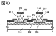
- 7A and 7B are conceptual diagrams of a passive matrix type light emitting device.
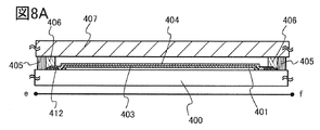
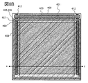
- 8A and 8B are diagrams showing a lighting device.
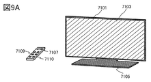
- 9A to 9D are diagrams showing electronic devices.
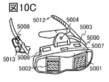
- 10A to 10C are diagrams showing electronic devices.
- FIG. 11 is a diagram showing a lighting device.
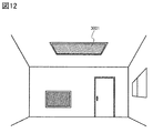
- FIG. 12 is a diagram showing a lighting device.
- FIG. 13 is a diagram showing an in-vehicle display device and a lighting device.
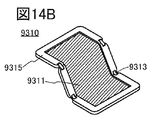
- 14A to 14C are diagrams showing electronic devices.
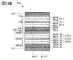
- 15A and 15B are diagrams illustrating a configuration of a light emitting device according to an embodiment.
- FIG. 16 is a diagram illustrating a current density-luminance characteristic of the light emitting device according to the embodiment.
- FIG. 17 is a diagram illustrating a luminance-current efficiency characteristic of the light emitting device according to the embodiment.
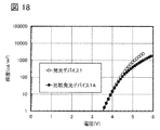
- FIG. 18 is a diagram illustrating a voltage-luminance characteristic of the light emitting device according to the embodiment.
- FIG. 19 is a diagram illustrating a voltage-current characteristic of the light emitting device according to the embodiment.
- FIG. 20 is a diagram for explaining the luminance-external quantum efficiency characteristics of the light emitting device according to the embodiment.
- FIG. 21 is a diagram illustrating an emission spectrum of a light emitting device according to an embodiment.
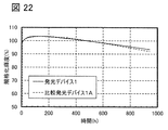
- FIG. 22 is a diagram illustrating standardized luminance-time change characteristics of the light emitting device according to the embodiment.
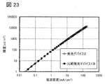
- FIG. 23 is a diagram illustrating a current density-luminance characteristic of the light emitting device according to the embodiment.
- FIG. 24 is a diagram illustrating a luminance-current efficiency characteristic of the light emitting device according to the embodiment.
- FIG. 25 is a diagram illustrating a voltage-luminance characteristic of the light emitting device according to the embodiment.
- FIG. 26 is a diagram illustrating a voltage-current characteristic of the light emitting device according to the embodiment.
- FIG. 27 is a diagram for explaining the luminance-external quantum efficiency characteristics of the light emitting device according to the embodiment.
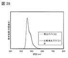
- FIG. 28 is a diagram illustrating an emission spectrum of a light emitting device according to an embodiment.
- FIG. 29 is a diagram illustrating standardized luminance-time change characteristics of the light emitting device according to the embodiment.
- FIG. 30 is a diagram illustrating a current density-luminance characteristic of the light emitting device according to the embodiment.
- FIG. 31 is a diagram illustrating a luminance-current efficiency characteristic of the light emitting device according to the embodiment.
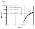
- FIG. 32 is a diagram illustrating a voltage-luminance characteristic of the light emitting device according to the embodiment.
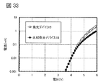
- FIG. 33 is a diagram illustrating a voltage-current characteristic of the light emitting device according to the embodiment.
- FIG. 34 is a diagram illustrating the luminance-external quantum efficiency characteristics of the light emitting device according to the embodiment.
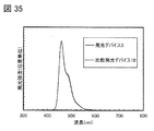
- FIG. 35 is a diagram illustrating an emission spectrum of a light emitting device according to an embodiment.
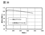
- FIG. 36 is a diagram illustrating standardized luminance-time change characteristics of the light emitting device according to the embodiment.
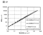
- FIG. 37 is a diagram illustrating a current density-luminance characteristic of the light emitting device according to the embodiment.
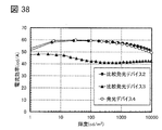
- FIG. 38 is a diagram illustrating a luminance-current efficiency characteristic of the light emitting device according to the embodiment.
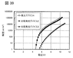
- FIG. 39 is a diagram illustrating a voltage-luminance characteristic of the light emitting device according to the embodiment.
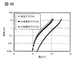
- FIG. 40 is a diagram for explaining the voltage-current characteristics of the light emitting device according to the embodiment.
- FIG. 41 is a diagram for explaining the luminance-external quantum efficiency characteristics of the light emitting device according to the embodiment.
- FIG. 42 is a diagram illustrating an emission spectrum of a light emitting device according to an embodiment.
- FIG. 43 is a diagram illustrating standardized luminance-time change characteristics of the light emitting device according to the embodiment.
- 44A and 44B are cross-sectional views illustrating the configuration of the light emitting device according to the embodiment.
- FIG. 45 is a diagram illustrating a current density-luminance characteristic of the light emitting device according to the embodiment.
- FIG. 46 is a diagram illustrating a luminance-current efficiency characteristic of the light emitting device according to the embodiment.
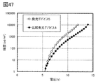
- FIG. 47 is a diagram illustrating a voltage-luminance characteristic of the light emitting device according to the embodiment.
- FIG. 48 is a diagram illustrating a voltage-current characteristic of the light emitting device according to the embodiment.
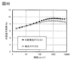
- FIG. 49 is a diagram for explaining the luminance-external quantum efficiency characteristics of the light emitting device according to the embodiment.
- FIG. 50 is a diagram illustrating an emission spectrum of a light emitting device according to an embodiment.
- FIG. 51 is a diagram illustrating standardized luminance-time change characteristics of the light emitting device according to the embodiment.
- the light emitting device of one aspect of the present invention has a first electrode, a second electrode, a unit, and a first layer.
- the second electrode comprises a region overlapping the first electrode, the unit comprises a region sandwiched between the first electrode and the second electrode, and the unit comprises a second layer and a third layer.
- the second layer comprises a region sandwiching the third layer from the first electrode, and the second layer contains a luminescent material.
- the first layer comprises a region sandwiched between the third layer and the first electrode.
- the first layer contains a material having acceptability and a first material, and the first layer includes a first region and a second region.
- the first region comprises a region sandwiched between the second region and the first electrode, the first region contains a material that is acceptable at the first concentration, and the second region is the second concentration. Includes materials that have acceptability in.
- the second concentration is higher than zero and lower than the first concentration.
- the drive voltage can be suppressed.
- the temperature dependence of the operating characteristics can be suppressed.
- the light emitting device 150 described in this embodiment includes an electrode 101, an electrode 102, a unit 103, and a layer 104 (see FIG. 1A).
- the electrode 102 includes a region that overlaps with the electrode 101.
- the unit 103 includes a region sandwiched between the electrodes 101 and 102, and the unit 103 includes layers 111 and 112.
- the electrode 101 can be used as an anode and the electrode 102 can be used as a cathode.
- a layer selected from functional layers such as a hole transport layer, an electron transport layer, a carrier block layer, and an exciton block layer can be used for the unit 103.
- the layer 111 includes a region sandwiching the layer 112 with the electrode 101, and the layer 111 contains a luminescent material EM.
- the layer 111 contains a host material. Further, the layer 111 can be called a light emitting layer. It is preferable that the layer 111 is arranged in the region where holes and electrons are recombined. As a result, the energy generated by the recombination of carriers can be efficiently converted into light and emitted. Further, it is preferable that the layer 111 is arranged away from the metal used for the electrode or the like. This makes it possible to suppress the quenching phenomenon caused by the metal used for the electrodes and the like.
- a fluorescent substance for example, a fluorescent substance, a phosphorescent substance, or a substance exhibiting a thermally activated delayed fluorescent TADF (Thermally Delayed Fluorescence) can be used as a luminescent material.
- TADF Thermally activated delayed fluorescent
- a fluorescent material can be used for layer 111.
- the fluorescent material illustrated below can be used for layer 111.
- various known fluorescent light emitting substances can be used for the layer 111.
- condensed aromatic diamine compounds typified by pyrenediamine compounds such as 1,6FLPAPrn, 1,6 mMFLPAPrn, and 1,6BnfAPrn-03 have high hole trapping properties and are excellent in luminous efficiency or reliability. preferable.
- a phosphorescent substance can be used for the layer 111.
- the phosphorescent material illustrated below can be used for layer 111.
- various known phosphorescent luminescent substances can be used for the layer 111.
- an organometallic iridium complex having a 4H-triazole skeleton or the like can be used for the layer 111.
- an organometallic iridium complex having a 1H-triazole skeleton or the like can be used.
- Tris [3-methyl-1- (2-methylphenyl) -5-phenyl-1H-1,2,4-triazolate] iridium (III) (abbreviation: [Ir (Mptz1-mp) 3 ]]
- Tris (1-methyl-5-phenyl-3-propyl-1H-1,2,4-triazolate) iridium (III) (abbreviation: [Ir (Prptz1-Me) 3 ]), etc.
- an organometallic iridium complex having an imidazole skeleton can be used.
- fac-tris [1- (2,6-diisopropylphenyl) -2-phenyl-1H-imidazole] iridium (III) (abbreviation: [Ir (iPrpmi) 3 ]
- tris [3- (2). , 6-Dimethylphenyl) -7-methylimidazole [1,2-f] phenanthriginato] iridium (III) (abbreviation: [Ir (dmimpt-Me) 3 ]
- Ir (dmimpt-Me) 3 phenanthriginato
- an organometallic iridium complex or the like having a phenylpyridine derivative having an electron-withdrawing group as a ligand can be used.
- an organometallic iridium complex having a pyrimidine skeleton or the like can be used for the layer 111.
- an organometallic iridium complex having a pyrimidine skeleton or the like can be used for the layer 111.
- tris (4-methyl-6-phenylpyrimidinato) iridium (III) (abbreviation: [Ir (mppm) 3 ]
- tris (4-t-butyl-6-phenylpyrimidinato) iridium tris (4-t-butyl-6-phenylpyrimidinato
- an organometallic iridium complex having a pyrazine skeleton or the like can be used.
- (acetylacetonato) bis (3,5-dimethyl-2-phenylpyrazinato) iridium (III) (abbreviation: [Ir (mppr-Me) 2 (acac)]), (acetylacetonato).
- Bis (5-isopropyl-3-methyl-2-phenylpyrazinato) iridium (III) (abbreviation: [Ir (mppr-iPr) 2 (acac)]), and the like can be used.
- an organometallic iridium complex having a pyridine skeleton or the like can be used. Specifically, tris (2-phenylpyridinato-N, C 2' ) iridium (III) (abbreviation: [Ir (ppy) 3 ]), bis (2-phenylpyridinato-N, C 2').
- Iridium (III) acetylacetonate abbreviation: [Ir (ppy) 2 (acac)]
- bis benzo [h] quinolinato) iridium (III) acetylacetonate
- Tris benzo [h] quinolinato) iridium (III) (abbreviation: [Ir (bzq) 3 ]
- tris tris (2- phenylquinolinato-N, C 2' ) iridium (III) (abbreviation: [Ir) (Pq) 3 ])
- bis 2-phenylquinolinato-N, C 2' ) iridium (III) acetylacetonate
- [Ir (pq) 2 (acac)] [2-d3-methyl- (2-Pyridinyl- ⁇ N) benzoflo [2,3-b] pyridine
- a rare earth metal complex or the like can be used.
- specific examples thereof include tris (acetylacetonato) (monophenanthroline) terbium (III) (abbreviation: [Tb (acac) 3 (Phen)]).
- these are compounds mainly exhibiting green phosphorescence emission, and have a peak of emission wavelength from 500 nm to 600 nm.
- the organometallic iridium complex having a pyrimidine skeleton is particularly preferable because it is remarkably excellent in reliability or luminous efficiency.
- an organometallic iridium complex having a pyrimidine skeleton or the like can be used for the layer 111.
- (diisobutyrylmethanato) bis [4,6-bis (3-methylphenyl) pyrimidinato] iridium (III) (abbreviation: [Ir (5mdppm) 2 (divm)]), bis [4,6 -Bis (3-methylphenyl) pyrimidinato] (dipivaloylmethanato) iridium (III) (abbreviation: [Ir (5mdppm) 2 (dpm)]
- bis [4,6-di (naphthalene-1-yl)) Pyrimidineat] dipivaloylmethanato) iridium (III) (abbreviation: [Ir (d1npm) 2 (dpm)]
- the like can be used.
- an organometallic iridium complex having a pyrazine skeleton or the like can be used.
- (acetylacetonato) bis (2,3,5-triphenylpyrazinato) iridium (III) (abbreviation: [Ir (tppr) 2 (acac)])
- bis (2,3,5) -Triphenylpyrazinato) (dipivaloylmethanato) iridium (III) (abbreviation: [Ir (tppr) 2 (dpm)]
- Kinoxarinato] Iridium (III) (abbreviation: [Ir (Fdpq) 2 (acac)]), etc.
- an organometallic iridium complex having a pyridine skeleton or the like can be used.
- Iridium (III) acetylacetonate (abbreviation: [Ir (piq) 2 (acac)]), etc. can be used.
- a platinum complex or the like can be used. Specifically, 2,3,7,8,12,13,17,18-octaethyl-21H, 23H-porphyrin platinum (II) (abbreviation: PtOEP), etc. can be used.
- a rare earth metal complex or the like can be used.
- Tris (1,3-diphenyl-1,3-propanedionat) (monophenanthroline) Europium (III) abbreviation: [Eu (DBM) 3 (Phen)]
- Tris [1- (2) -Tenoyl) -3,3,3-trifluoroacetonato] diophenanthroline) Europium (III)
- Eu (TTA) 3 (Phen)] can be used.
- organometallic iridium complex having a pyrazine skeleton can obtain red light emission having a chromaticity that can be satisfactorily used in a display device.
- a substance exhibiting Thermally Activated Delayed Fluorescence (also referred to as TADF material) can be used for layer 111.
- TADF material also referred to as TADF material
- the TADF material illustrated below can be used for layer 111.
- various known TADF materials can be used for the layer 111.
- fullerenes and derivatives thereof, acridine and derivatives thereof, eosin derivatives and the like can be used as TADF materials.
- a metal-containing porphyrin containing magnesium (Mg), zinc (Zn), cadmium (Cd), tin (Sn), platinum (Pt), indium (In), palladium (Pd) and the like can be used as the TADF material. can.
- protoporphyrin-tin fluoride complex SnF 2 (Proto IX)
- mesoporphyrin-tin fluoride complex SnF 2 (Meso IX)
- hematoporphyrin-tin fluoride SnF 2 (Proto IX)
- protoporphyrin-tin fluoride complex SnF 2 (Proto IX)
- mesoporphyrin-tin fluoride complex SnF 2 (Meso IX)
- hematoporphyrin-tin fluoride hematoporphyrin-tin fluoride
- a heterocyclic compound having one or both of a ⁇ -electron excess heteroaromatic ring and a ⁇ -electron deficiency heteroaromatic ring can be used as the TADF material.
- the heterocyclic compound has a ⁇ -electron excess type heteroaromatic ring and a ⁇ -electron deficiency type heteroaromatic ring, both electron transportability and hole transportability are high, which is preferable.
- the skeletons having a ⁇ -electron deficient heteroaromatic ring the pyridine skeleton, the diazine skeleton (pyrimidine skeleton, pyrazine skeleton, pyridazine skeleton), and triazine skeleton are preferable because they are stable and have good reliability.
- the benzoflopyrimidine skeleton, the benzothienopyrimidine skeleton, the benzoflopyrazine skeleton, and the benzothienopyrazine skeleton are preferable because they have high acceptability and good reliability.
- the acridine skeleton, the phenoxazine skeleton, the phenothiazine skeleton, the furan skeleton, the thiophene skeleton, and the pyrrole skeleton are stable and have good reliability, and therefore at least one of the skeletons. It is preferable to have.
- the furan skeleton is preferably a dibenzofuran skeleton
- the thiophene skeleton is preferably a dibenzothiophene skeleton.
- an indole skeleton, a carbazole skeleton, an indolecarbazole skeleton, a bicarbazole skeleton, and a 3- (9-phenyl-9H-carbazole-3-yl) -9H-carbazole skeleton are particularly preferable.
- the substance in which the ⁇ -electron-rich heteroaromatic ring and the ⁇ -electron-deficient heteroaromatic ring are directly bonded has both the electron donating property of the ⁇ -electron-rich heteroaromatic ring and the electron acceptability of the ⁇ -electron-deficient heteroaromatic ring. It becomes stronger and the energy difference between the S1 level and the T1 level becomes smaller, which is particularly preferable because the heat-activated delayed fluorescence can be efficiently obtained.
- an aromatic ring to which an electron-withdrawing group such as a cyano group is bonded may be used.
- an aromatic amine skeleton, a phenazine skeleton, or the like can be used as the ⁇ -electron excess type skeleton.
- An aromatic ring or heteroaromatic ring having a group or a cyano group, a carbonyl skeleton such as benzophenone, a phosphine oxide skeleton, a sulfone skeleton and the like can be used.
- a ⁇ -electron-deficient skeleton and a ⁇ -electron-rich skeleton can be used instead of at least one of the ⁇ -electron-deficient heteroaromatic ring and the ⁇ -electron-rich heteroaromatic ring.
- the TADF material is a material having a small difference between the S1 level and the T1 level and having a function of converting energy from triplet excitation energy to singlet excitation energy by intersystem crossing. Therefore, the triplet excited energy can be up-converted to the singlet excited energy by a small amount of heat energy (intersystem crossing), and the singlet excited state can be efficiently generated. In addition, triplet excitation energy can be converted into light emission.
- an excited complex also referred to as an exciplex, an exciplex or an Exciplex
- the difference between the S1 level and the T1 level is extremely small, and the triplet excitation energy is the singlet excitation energy. It has a function as a TADF material that can be converted into.
- a phosphorescence spectrum observed at a low temperature may be used.
- a tangent line is drawn at the hem on the short wavelength side of the fluorescence spectrum
- the energy of the wavelength of the extraline is set to the S1 level
- a tangent line is drawn at the hem on the short wavelength side of the phosphorescence spectrum, and the extrapolation thereof is performed.
- the difference between S1 and T1 is preferably 0.3 eV or less, and more preferably 0.2 eV or less.
- the S1 level of the host material is preferably higher than the S1 level of the TADF material.
- the T1 level of the host material is preferably higher than the T1 level of the TADF material.
- the layer 104 includes a region sandwiched between the layer 112 and the electrode 101 (see FIG. 1A).
- Layer 104 contains material AM and material HT1 having acceptability.
- the material containing the material AM and the material HT1 having acceptability can be said to be a composite material.
- Material AM with acceptor properties For example, a compound having an electron-withdrawing group (halogen group or cyano group) can be used as a material having acceptability. It should be noted that the organic compound having acceptor property is easy to be deposited and easily formed. This makes it possible to increase the productivity of the light emitting device.
- a compound such as HAT-CN in which an electron-withdrawing group is bonded to a condensed aromatic ring having a plurality of complex atoms is thermally stable and preferable.
- the [3] radialene derivative having an electron-withdrawing group is preferable because it has very high electron acceptability.
- ⁇ , ⁇ ', ⁇ ''-1,2,3-cyclopropanetriylidentris [4-cyano-2,3,5,6-tetrafluorobenzene acetonitrile]
- ⁇ , ⁇ ', ⁇ ' '-1,2,3-Cyclopropanetriylidentris [2,6-dichloro-3,5-difluoro-4- (trifluoromethyl) benzeneacetonitrile]
- ⁇ , ⁇ ', ⁇ ''-1,2, 3-Cyclopropanetriylidentris [2,3,4,5,6-pentafluorobenzeneacetonitrile] and the like can be used.
- Material HT1 For example, a material having hole transportability can be used for the material HT1.
- the material having hole transportability it is preferable that the material has a hole mobility of 1 ⁇ 10-6 cm 2 / Vs or more.
- a compound having an aromatic amine skeleton, a compound having a carbazole skeleton, a compound having a thiophene skeleton, a compound having a furan skeleton, and the like can be used.
- an amine compound or an organic compound having a ⁇ -electron excess type heteroaromatic ring skeleton is preferable.
- a compound having an aromatic amine skeleton, a compound having a carbazole skeleton, a compound having a thiophene skeleton, a compound having a furan skeleton, and the like can be used.
- Examples of the compound having an aromatic amine skeleton include 4,4'-bis [N- (1-naphthyl) -N-phenylamino] biphenyl (abbreviation: NPB) and N, N'-bis (3-methylphenyl).
- Examples of the compound having a carbazole skeleton include 1,3-bis (N-carbazolyl) benzene (abbreviation: mCP), 4,4'-di (N-carbazolyl) biphenyl (abbreviation: CBP), and 3,6-bis. (3,5-Diphenylphenyl) -9-phenylcarbazole (abbreviation: CzTP), 3,3'-bis (9-phenyl-9H-carbazole) (abbreviation: PCCP), and the like can be used.
- mCP 1,3-bis (N-carbazolyl) benzene
- CBP 4,4'-di (N-carbazolyl) biphenyl
- PCCP 3,6-bis.
- Examples of the compound having a thiophene skeleton include 4,4', 4''-(benzene-1,3,5-triyl) tri (dibenzothiophene) (abbreviation: DBT3P-II), 2,8-diphenyl-4. -[4- (9-Phenyl-9H-fluorene-9-yl) phenyl] dibenzothiophene (abbreviation: DBTFLP-III), 4- [4- (9-phenyl-9H-fluorene-9-yl) phenyl]- 6-Phenyldibenzothiophene (abbreviation: DBTFLP-IV), etc. can be used.
- Examples of the compound having a furan skeleton include 4,4', 4''- (benzene-1,3,5-triyl) tri (dibenzofuran) (abbreviation: DBF3P-II), 4- ⁇ 3- [3- [3-]. (9-Phenyl-9H-fluorene-9-yl) phenyl] phenyl ⁇ dibenzofuran (abbreviation: mmDBFFLBi-II), etc. can be used.
- the compound having an aromatic amine skeleton or the compound having a carbazole skeleton is preferable because it has good reliability, high hole transportability, and contributes to reduction of driving voltage.
- Layer 104 comprises regions 104A and 104B.
- the region 104A comprises a region sandwiched between the region 104B and the electrode 101, and the region 104A contains a material AM having acceptability at a concentration C1.
- the concentration containing the material having acceptability there is a distribution in the concentration containing the material having acceptability.
- Region 104B contains material AM having acceptability at concentration C2, concentration C2 being higher than zero and lower than concentration C1.
- the drive voltage can be suppressed.
- the temperature dependence of the operating characteristics can be suppressed.
- the unit 103 includes a layer 113 (see FIG. 1A).
- the layer 113 comprises a region sandwiched between the electrode 102 and the layer 111, and the layer 113 contains the material OMC.
- the material OMC is an organic complex of an alkali metal or an organic complex of an alkaline earth metal.
- a material containing an alkali metal, an alkali metal compound or an alkali metal complex and a substance having an electron transporting property can be used as a material having an electron transporting property.
- a substance having a relatively deep HOMO level of -5.7 eV or more and -5.4 eV or less is used for the composite material of the hole injection layer, the reliability of the light emitting device can be improved. .. It is more preferable that the HOMO level of the material having electron transportability is ⁇ 6.0 eV or more.
- it preferably contains an 8-hydroxyquinolinato structure.
- 8-hydroxyquinolinato-lithium abbreviation: Liq
- 8-hydroxyquinolinato-sodium abbreviation: Naq
- the like can be used.
- a monovalent metal ion complex particularly a lithium complex
- Liq is more preferable.
- it contains an 8-hydroxyquinolinato structure its methyl-substituted product (for example, 2-methyl-substituted product or 5-methyl-substituted product) or the like can also be used.
- a simple substance, a compound or a complex of an alkali metal or an alkaline earth metal has a concentration difference (including the case where it is 0) in the thickness direction thereof.
- Layer 112 comprises regions 112A and 112B.
- the region 112B includes a region sandwiched between the layer 111 and the region 112A, and the region 112B contains the material HT2.
- a material having hole transport properties can be used for layer 112.
- a material having hole transport properties that can be used for layer 104 can be used for material HT2.
- the layer 112 can be called a hole transport layer. It is preferable that a substance having a bandgap larger than the bandgap of the luminescent material contained in the layer 111 is used for the region 112B. As a result, the energy transfer from the excitons generated in the layer 111 to the region 112B can be suppressed.
- the material HT1 includes a first HOMO level HOMO1, and the first HOMO level HOMO1 is ⁇ 5.7 eV or more and ⁇ 5.4 eV or less (see FIG. 1B). Further, the material HT2 includes a second HOMO level HOMO2, and the second HOMO level HOMO2 is in the range of ⁇ 0.2 ev or more and 0 ev or less with respect to the first HOMO level HOMO1.
- the layer 111 includes the host material HOST, and the host material HOST includes the first LUMO level LUMO 1 (see FIG. 1B).
- a material having carrier transportability can be used for the host material HOST.
- a material having a hole transporting property, a material having an electron transporting property, a TADF material, a material having an anthracene skeleton, a mixed material and the like can be used as a host material.
- a hole-transporting material that can be used for layer 112 can be used for the host material HOST.
- An organic compound having an anthracene skeleton can be used as a material having electron transportability.
- an organic compound containing both an anthracene skeleton and a heterocyclic skeleton can be preferably used.
- an organic compound containing both an anthracene skeleton and a nitrogen-containing 5-membered ring skeleton or an organic compound containing both an anthracene skeleton and a nitrogen-containing 6-membered ring skeleton can be used.
- an organic compound containing both a nitrogen-containing 5-membered ring skeleton and an anthracene skeleton containing two complex atoms in the ring or an organic compound having a nitrogen-containing 6-membered ring skeleton containing two complex atoms in the ring can be used.
- a pyrazole ring an imidazole ring, an oxazole ring, a thiazole ring, a pyrazine ring, a pyrimidine ring, a pyridazine ring and the like can be preferably used for the heterocyclic skeleton.
- a metal complex or an organic compound having a ⁇ -electron deficient heteroaromatic ring skeleton is preferable.
- the organic compound having a ⁇ -electron-deficient heteroarocyclic skeleton for example, a heterocyclic compound having a polyazole skeleton, a heterocyclic compound having a diazine skeleton, and a heterocyclic compound having a pyridine skeleton are preferable.
- a heterocyclic compound having a diazine skeleton or a heterocyclic compound having a pyridine skeleton is preferable because it has good reliability.
- the heterocyclic compound having a diazine (pyrimidine or pyrazine) skeleton has high electron transport property and can reduce the driving voltage.
- Examples of the metal complex include bis (10-hydroxybenzo [h] quinolinato) berylium (II) (abbreviation: BeBq 2 ), bis (2-methyl-8-quinolinolato) (4-phenylphenolato) aluminum (III).
- BAlq bis (8-quinolinolato) zinc (II) (abbreviation: Znq)
- bis [2- (2-benzoxazolyl) phenolato] zinc (II) abbreviation: ZnPBO
- bis [2- (2-Benzothiazolyl) phenolato] Zinc (II) abbreviation: ZnBTZ
- heterocyclic compound having a polyazole skeleton examples include 2- (4-biphenylyl) -5- (4-tert-butylphenyl) -1,3,4-oxadiazole (abbreviation: PBD) and 3- (4).
- heterocyclic compound having a diazine skeleton examples include 2- [3- (dibenzothiophen-4-yl) phenyl] dibenzo [f, h] quinoxaline (abbreviation: 2mDBTPDBq-II) and 2- [3'-(dibenzo).
- heterocyclic compound having a pyridine skeleton examples include 3,5-bis [3- (9H-carbazole-9-yl) phenyl] pyridine (abbreviation: 35DCzPPy) and 1,3,5-tri [3- (3). -Pyridine) phenyl] benzene (abbreviation: TmPyPB), etc. can be used.
- the TADF material exemplified above can be used as the host material.
- the triplet excitation energy generated by the TADF material is converted into singlet excitation energy by the inverse intersystem crossing, and the energy is further transferred to the luminescent material to improve the emission efficiency of the light emitting device. be able to.
- the TADF material functions as an energy donor, and the luminescent material functions as an energy acceptor.
- the S1 level of the TADF material is preferably higher than the S1 level of the fluorescent light emitting substance.
- the T1 level of the TADF material is preferably higher than the S1 level of the fluorescent light emitting substance. Therefore, the T1 level of the TADF material is preferably higher than the T1 level of the fluorescent substance.
- a TADF material that emits light having a wavelength that overlaps with the wavelength of the absorption band on the lowest energy side of the fluorescent light emitting substance.
- the fluorescent substance preferably has a protecting group around the chromophore (skeleton that causes light emission) of the fluorescent substance.
- a protecting group a substituent having no ⁇ bond is preferable, a saturated hydrocarbon is preferable, specifically, an alkyl group having 3 or more and 10 or less carbon atoms, and a substituted or unsubstituted cyclo having 3 or more and 10 or less carbon atoms.
- Examples thereof include an alkyl group and a trialkylsilyl group having 3 or more and 10 or less carbon atoms, and it is more preferable that there are a plurality of protecting groups.
- Substituents that do not have ⁇ bonds have a poor ability to transport carriers, so they can increase the distance between the TADF material and the chromophore of the fluorescent luminescent material with little effect on carrier transport or carrier recombination. ..
- the chromophore refers to an atomic group (skeleton) that causes light emission in a fluorescent luminescent substance.
- the chromophore preferably has a skeleton having a ⁇ bond, preferably contains an aromatic ring, and preferably has a condensed aromatic ring or a condensed heteroaromatic ring.
- Examples of the condensed aromatic ring or the condensed heteroaromatic ring include a phenanthrene skeleton, a stilbene skeleton, an acridone skeleton, a phenoxazine skeleton, and a phenothiazine skeleton.
- a fluorescent substance having a naphthalene skeleton, anthracene skeleton, fluorene skeleton, chrysene skeleton, triphenylene skeleton, tetracene skeleton, pyrene skeleton, perylene skeleton, coumarin skeleton, quinacridone skeleton, and naphthobisbenzofuran skeleton is preferable because of its high fluorescence quantum yield.
- a material having an anthracene skeleton is suitable as the host material.
- a substance having an anthracene skeleton is used as a host material for a fluorescent light emitting substance, it is possible to realize a light emitting layer having good luminous efficiency and durability.
- a substance having an anthracene skeleton used as the host material a substance having a diphenylanthracene skeleton, particularly a substance having a 9,10-diphenylanthracene skeleton is preferable because it is chemically stable.
- the host material has a carbazole skeleton, it is preferable because the injection / transportability of holes is enhanced, but when the host material contains a benzocarbazole skeleton in which a benzene ring is further condensed with carbazole, the HOMO is about 0.1 eV shallower than that of carbazole. , It is more preferable because holes can easily enter.
- the host material contains a dibenzocarbazole skeleton
- the HOMO is about 0.1 eV shallower than that of carbazole, holes are easily entered, and the hole transport property is excellent and the heat resistance is also high, which is suitable. .. Therefore, a substance having a 9,10-diphenylanthracene skeleton and a carbazole skeleton (or a benzocarbazole skeleton or a dibenzocarbazole skeleton) at the same time is further preferable as a host material. From the viewpoint of hole injection / transportability, a benzofluorene skeleton or a dibenzofluorene skeleton may be used instead of the carbazole skeleton.
- Examples of the substance having an anthracene skeleton include 9-phenyl-3- [4- (10-phenyl-9-anthryl) phenyl] -9H-carbazole (abbreviation: PCzPA) and 3- [4- (1-naphthyl).
- CzPA, cgDBCzPA, 2mbnfPPA and PCzPA show very good properties.
- a material obtained by mixing a plurality of kinds of substances can be used as a host material.
- a material obtained by mixing a material having an electron transporting property and a material having a hole transporting property can be preferably used as a host material.
- the carrier transporting property of the layer 111 can be easily adjusted.
- the recombination region can be easily controlled.
- a material mixed with a phosphorescent substance can be used as a host material.
- the phosphorescent substance can be used as an energy donor that supplies excitation energy to the fluorescent substance when the fluorescent substance is used as the light emitting substance.
- a mixed material containing a material forming an excitation complex can be used as the host material.
- a material whose emission spectrum of the formed excitation complex overlaps with the wavelength of the absorption band on the lowest energy side of the luminescent substance can be used as the host material.
- the drive voltage can be suppressed.
- At least one of the materials forming the excitation complex may be a phosphorescent substance.
- the HOMO level of the material having hole transportability is equal to or higher than the HOMO level of the material having electron transportability.
- the LUMO level of the material having hole transportability is equal to or higher than the LUMO level of the material having electron transportability.
- the LUMO level and HOMO level of the material can be derived from the electrochemical properties (reduction potential and oxidation potential) of the material measured by cyclic voltammetry (CV) measurement.
- the emission spectrum of the material having hole transporting property, the emission spectrum of the material having electron transporting property, and the emission spectrum of the mixed film in which these materials are mixed are compared, and the emission spectrum of the mixed film is compared.
- the transient photoluminescence (PL) of the material having hole transportability, the transient PL of the material having electron transportability, and the transient PL of the mixed membrane in which these materials are mixed are compared, and the transient PL lifetime of the mixed membrane is determined.
- transient PL may be read as transient electroluminescence (EL). That is, by comparing the transient EL of the material having hole transporting property, the transient EL of the material having electron transporting property, and the transient EL of the mixed membrane of these, and observing the difference in the transient response, the formation of the excited complex can be formed. You can check.
- EL transient electroluminescence
- the unit 103 also includes a layer 113 (see FIG. 1A).
- ⁇ Configuration example 2 of layer 113 For example, a material having electron transportability can be used for layer 113. Further, the layer 113 can be called an electron transport layer. It is preferable that a substance having a bandgap larger than the bandgap of the luminescent material contained in the layer 111 is used for the layer 113. As a result, the energy transfer from the excitons generated in the layer 111 to the layer 113 can be suppressed.
- the electron mobility at a square root of electric field strength [V / cm] of 600 is 1 ⁇ 10-7 cm 2 / Vs or more and 5 ⁇ 10-5 cm 2 / Vs or less. preferable.
- the amount of electrons injected into the light emitting layer can be controlled. Alternatively, it is possible to prevent the light emitting layer from being in a state of excess electrons.
- a material having electron transportability that can be used for layer 111 can be used for layer 113.
- a material having electron transportability that can be used as a host material can be used for the layer 113.
- the layer 113 includes a region 113A and a region 113B.
- the region 113A comprises a region sandwiched between the region 113B and the layer 111, and the region 113A includes the material ET.
- the region 113B includes the material OMC.
- the material ET comprises a second LUMO level LUMO2, and the second LUMO level LUMO2 is -0.4 eV or more and -0.1 eV or less, preferably -0.4 eV, relative to the first LUMO level LUMO1. It is in the range of ⁇ 0.15 eV or less (see FIG. 1B).
- Configuration example 3 of layer 104 >> Further, in one aspect of the present invention, the region 104A is in contact with the electrode 101.
- a conductive material can be used for the electrode 101.
- a metal, an alloy, a conductive compound, a mixture thereof, or the like can be used for the electrode 101.
- a material having a work function of 4.0 eV or more can be preferably used.
- ITO Indium Tin Oxide
- indium tin oxide containing silicon or silicon oxide indium tin oxide-zinc oxide
- tungsten oxide and indium oxide containing zinc oxide IWZO are used. be able to.
- gold Au
- platinum Pt
- nickel Ni
- tungsten W
- Cr chromium
- Mo molybdenum
- iron Fe
- Co cobalt
- Cu copper
- palladium Pd
- a nitride of a metallic material for example, titanium nitride
- graphene can be used.
- a conductive material can be used for the electrode 102.
- metals, alloys, electrically conductive compounds, and mixtures thereof can be used for the electrode 102.
- a material having a work function smaller than that of the electrode 101 can be used for the electrode 102.
- a material having a work function of 3.8 eV or less can be preferably used.
- an element belonging to Group 1 of the Periodic Table of the Elements, an element belonging to Group 2 of the Periodic Table of the Elements, a rare earth metal, and an alloy containing these can be used for the electrode 102.
- lithium (Li), cesium (Cs) and the like, magnesium (Mg), calcium (Ca), strontium (Sr) and the like, europium (Eu), ytterbium (Yb) and the like, and alloys containing these (MgAg, AlLi) can be used for the electrode 102.
- the light emitting device 150 described in this embodiment has a layer 105.
- the layer 105 includes a region sandwiched between the electrodes 102 and the unit 103.
- a material with electron injectability can be used for layer 105.
- a substance having a donor property can be used for the layer 105.
- a composite material in which a substance having a donor property is contained in a material having an electron transport property can be used for the layer 105. This makes it easier to inject electrons from, for example, the electrode 102.
- the drive voltage of the light emitting device can be reduced.
- various conductive materials can be used for the electrode 102 regardless of the magnitude of the work function. Specifically, indium-tin oxide containing Al, Ag, ITO, silicon or silicon oxide can be used for the electrode 102.
- alkali metals, alkaline earth metals, rare earth metals or compounds thereof can be used as substances having donor properties.
- an organic compound such as tetrathianaphthalene (abbreviation: TTN), nickelocene, or decamethylnickelocene can be used as a substance having donor properties.
- alkali metal compounds including oxides, halides and carbonates
- alkaline earth metal compounds including oxides, halides and carbonates
- rare earth metal compounds oxides, halides, (Including carbonate)
- lithium oxide lithium fluoride (LiF), cesium fluoride (CsF), calcium fluoride (CaF 2 ), lithium carbonate, cesium carbonate, 8-hydroxyquinolinato-lithium (abbreviation: Liq) and the like are used.
- a composite material containing an alkali metal or an alkaline earth metal or a compound thereof and a substance having an electron transporting property can be used as a material having an electron injecting property.
- a material having an electron transporting property that can be used for the unit 103 can be used as a material having an electron injecting property.
- a material containing a microcrystalline alkali metal fluoride and a substance having an electron transporting property or a material containing a microcrystalline alkaline earth metal fluoride and a substance having an electron transporting property can be electron-injectable. Can be used for materials having.
- a material containing 50 wt% or more of alkali metal fluoride or alkaline earth metal fluoride can be preferably used.
- an organic compound having a bipyridine skeleton can be preferably used.
- the refractive index of the layer 105 can be reduced.
- the external quantum efficiency of the light emitting device can be improved.
- electride can be used as a material having electron injectability.
- a substance in which electrons are added at a high concentration to a mixed oxide of calcium and aluminum can be used as a material having electron injectability.
- FIG. 2A is a cross-sectional view illustrating the configuration of a light emitting device according to an aspect of the present invention, which has a configuration different from the configuration shown in FIG.
- the light emitting device 150 described in this embodiment includes an electrode 101, an electrode 102, a unit 103, an intermediate layer 106, and a unit 103 (12) (see FIG. 2A). Further, layers 104 (12) and 105 (12) can be used.
- the same configuration as the layer 104 described in the first embodiment can be used for the layer 104 (12), and the same configuration as the layer 105 described in the first embodiment can be used for the layer 105 (12). can.
- the unit 103 includes a region sandwiched between the electrodes 101 and 102, the unit 103 (12) includes a region sandwiched between the electrodes 101 and 103, and the intermediate layer 106 is a region of the unit 103 (12) and the unit 103. It has an area sandwiched between them. Further, the layer 105 (12) includes a region sandwiched between the unit 103 (12) and the intermediate layer 106.
- the light emitting device 150 has a plurality of stacked units.
- the number of the plurality of stacked units is not limited to 2, and 3 or more units can be laminated.
- the configuration including the intermediate layer 106 and a plurality of units may be referred to as a laminated light emitting device or a tandem type light emitting device. This makes it possible to emit high-intensity light while keeping the current density low. Alternatively, reliability can be improved. Alternatively, the drive voltage can be reduced by comparing with the same brightness. Alternatively, power consumption can be suppressed.
- Configuration example of unit 103 (12) The configuration that can be used for the unit 103 can be used for the unit 103 (12). For example, the same configuration as the unit 103 can be used for the unit 103 (12).
- a configuration different from the unit 103 can be used for the unit 103 (12).
- a configuration of an emission color different from the emission color of the unit 103 can be used for the unit 103 (12).
- a unit 103 that emits red light and green light and a unit 103 (12) that emits blue light can be used. This makes it possible to provide a light emitting device that emits light of a desired color. Alternatively, for example, a light emitting device that emits white light can be provided.
- the intermediate layer 106 includes a layer 104 and a layer 106A.
- the intermediate layer 106 has a function of supplying electrons to one of the unit 103 and the unit 103 (12) and supplying holes to the other.
- Layer 104 comprises material AM and material HT1 having acceptability
- layer 104 comprises regions 104A and 104B.
- the region 104A includes a region sandwiched between the region 104B and the electrode 101, and the region 104A contains a material AM having acceptability at a concentration C1.
- Region 104B contains material AM having acceptability at concentration C2, concentration C2 being higher than zero and lower than concentration C1.
- the drive voltage can be suppressed.
- the temperature dependence of the operating characteristics can be suppressed.
- the layer 104 can be referred to as a charge generation layer.
- the charge generation layer has a function of supplying electrons to the anode side and holes to the cathode side by applying a voltage. Specifically, electrons can be supplied to the unit 103 (12) arranged on the anode side.
- Layer 106A comprises a region sandwiched between layer 104 and unit 103 (12).
- the layer 106A can be referred to as, for example, an electronic relay layer.
- a substance having electron transportability can be used for the electron relay layer.
- the layer in contact with the anode side of the electron relay layer can be kept away from the layer in contact with the cathode side of the electron relay layer.
- the interaction between the layer in contact with the anode side of the electron relay layer and the layer in contact with the cathode side of the electron relay layer can be reduced.
- electrons can be smoothly supplied to the layer in contact with the anode side of the electron relay layer.
- a substance having electron transportability can be preferably used for the electron relay layer.
- a substance having a LUMO level between the LUMO level of the material AM having acceptability used for the layer 104 and the LUMO level of the material HT1 having the hole transport property used for the layer 104 is placed in an electron. It can be suitably used for a relay layer.
- a substance having an electron transporting property having a LUMO level in the range of ⁇ 5.0 eV or more, preferably ⁇ 5.0 eV or more and ⁇ 3.0 eV or less can be used for the electron relay layer.
- a phthalocyanine-based material can be used for the electronic relay layer.
- a metal complex having a metal-oxygen bond and an aromatic ligand can be used for the electron relay layer.
- FIG. 2B is a cross-sectional view illustrating the configuration of a light emitting device according to an aspect of the present invention, which has a configuration different from the configuration shown in FIG.
- the light emitting device 150 described in the present embodiment has an electrode 101, an electrode 102, a unit 103, a layer 104, and an intermediate layer 106 (see FIG. 2B).
- the light emitting device 150 is different from the configuration shown in FIG. 1 in that the intermediate layer 106 is provided between the layer 105 and the electrodes 102.
- the different parts will be described in detail, and the above description will be incorporated for the parts where the same configuration can be used.
- the intermediate layer 106 includes a region sandwiched between the unit 103 and the electrodes 102, and the intermediate layer 106 includes layers 106A and 106B.
- Layer 106A comprises a region sandwiched between layers 106B and 105.
- the electronic relay layer described in the second embodiment can be used for the layer 106A.
- the layer 106B can be referred to as, for example, a charge generation layer.
- the charge generation layer has a function of supplying electrons to the anode side and holes to the cathode side by applying a voltage. Specifically, electrons can be supplied to the unit 103 arranged on the anode side.
- a composite material exemplified as a material having hole injection property can be used for the charge generation layer.
- a laminated film in which a film containing the composite material and a film containing a material having a hole transport property are laminated can be used as the charge generation layer.
- each layer of the electrode 101, the electrode 102, the unit 103, and the intermediate layer 106 can be formed by using a dry method, a wet method, a vapor deposition method, a droplet ejection method, a coating method, a printing method, or the like. Further, each layer of the unit 103 (12) can also be formed by using the same method. Also, different methods can be used to form each configuration.
- the light emitting device 150 can be manufactured by using a vacuum deposition apparatus, an inkjet apparatus, a coating apparatus such as a spin coater, a gravure printing apparatus, an offset printing apparatus, a screen printing apparatus, and the like.
- the electrode can be formed by a wet method using a paste of a metallic material or a sol-gel method.
- an indium oxide-zinc oxide film can be formed by a sputtering method using a target in which 1 to 20 wt% zinc oxide is added to indium oxide.
- a target containing 0.5 to 5 wt% of tungsten oxide and 0.1 to 1 wt% of zinc oxide with respect to indium oxide an indium oxide (IWZO) film containing tungsten oxide and zinc oxide was formed by a sputtering method. Can be formed.
- the light emitting panel 700 described in this embodiment has a light emitting device 150 and a light emitting device 150 (2) (FIG. 3).
- the light emitting device described in any one of the first to third embodiments can be used for the light emitting device 150.
- the light emitting device 150 (2) described in this embodiment includes an electrode 101 (2), an electrode 102, and a unit 103 (2) (see FIG. 3).
- a part of the configuration of the light emitting device 150 can be used as a part of the configuration of the light emitting device 150 (2).
- a part of the configuration can be made common.
- the manufacturing process can be simplified.
- the unit 103 (2) includes a region sandwiched between the electrode 101 (2) and the electrode 102. Further, the unit 103 (2) includes a layer 111 (2). For example, a luminescent material that emits light of a color different from that of the layer 111 included in the unit 103 can be used for the layer 111 (2).
- the unit 103 (2) has a single-layer structure or a laminated structure.
- a layer selected from functional layers such as a hole transport layer, an electron transport layer, a carrier block layer, and an exciton block layer can be used for the unit 103 (2).
- Unit 103 (2) includes a region in which the electrons injected from one electrode recombine with the holes injected from the other electrode. For example, it includes a region in which the holes injected from the electrode 101 (2) recombine with the electrons injected from the electrode 102.
- Layer 104 (2) comprises a region sandwiched between the electrode 101 and the unit 103.
- the layer 104 (2) can be referred to as a hole injection layer.
- a material having hole injectability can be used for layer 104 (2).
- accepting materials and composite materials can be used for layer 104 (2).
- an organic compound and an inorganic compound can be used as a material having acceptability.
- the accepting material can extract electrons from the adjacent hole transport layer (or hole transport material).
- Example 1 of a material having hole injection property A material having an accepting property can be used as a material having a hole injecting property. This makes it easier to inject holes from the electrode 101, for example. Alternatively, the drive voltage of the light emitting device can be reduced.
- the material having acceptability described in the first embodiment can be used as the material having hole injection property.
- molybdenum oxide, vanadium oxide, ruthenium oxide, tungsten oxide, manganese oxide and the like can be used as a material having acceptability.
- phthalocyanine abbreviation: H 2 Pc
- copper phthalocyanine complex phthalocyanine-based compound such as 4,4'-bis [N-(4-diphenylaminophenyl) -N- phenylamino] biphenyl (abbreviation: DPAB), N, N'-bis ⁇ 4- [bis (3-methylphenyl) amino] phenyl ⁇ -N, N'-diphenyl- (1,1'-biphenyl) -4,4'-diamine (abbreviation: A compound having an aromatic amine skeleton such as DNTPD) can be used.
- DPAB 4,4'-bis [N-(4-diphenylaminophenyl) -N- phenylamino] biphenyl
- DPAB 4,4'-bis [N-(4-diphenylaminophenyl) -N- phenylamino] biphenyl
- polymers such as poly (3,4-ethylenedioxythiophene) / poly (styrene sulfonic acid) (PEDOT / PSS) can be used.
- the composite material can be used as a material having hole injection property.
- a composite material in which a material having a hole transporting property and a material having an accepting property are contained can be used.
- the material forming the electrode can be selected in a wide range regardless of the work function.
- a material having a large work function but also a material having a small work function can be used for the electrode 101.
- Various organic compounds can be used in the hole-transporting material of the composite material.
- a compound having an aromatic amine skeleton, a carbazole derivative, an aromatic hydrocarbon, a polymer compound (oligomer, dendrimer, polymer, etc.) and the like can be used as a material having a hole transport property of a composite material.
- a substance having a hole mobility of 1 ⁇ 10 -6 cm 2 / Vs or more can be preferably used.
- a substance having a relatively deep HOMO level having a HOMO level of ⁇ 5.7 eV or more and ⁇ 5.4 eV or less can be preferably used as a material having a hole transport property of a composite material. This makes it possible to facilitate the injection of holes into the hole transport layer. Alternatively, the reliability of the light emitting device can be improved.
- Examples of the compound having an aromatic amine skeleton include N, N'-di (p-tolyl) -N, N'-diphenyl-p-phenylenediamine (abbreviation: DTDPPA), 4,4'-bis [N- (4-Diphenylaminophenyl) -N-phenylamino] biphenyl (abbreviation: DPAB), N, N'-bis ⁇ 4- [bis (3-methylphenyl) amino] phenyl ⁇ -N, N'-diphenyl-( 1,1'-biphenyl) -4,4'-diamine (abbreviation: DNTPD), 1,3,5-tris [N- (4-diphenylaminophenyl) -N-phenylamino] benzene (abbreviation: DPA3B), Etc. can be used.
- DTDPPA 4,4'-bis [N- (4-Diphenylaminophenyl) -N
- carbazole derivative examples include 3- [N- (9-phenylcarbazole-3-yl) -N-phenylamino] -9-phenylcarbazole (abbreviation: PCzPCA1) and 3,6-bis [N- (9-).
- Phenylcarbazole-3-yl) -N-phenylamino] -9-phenylcarbazole (abbreviation: PCzPCA2), 3- [N- (1-naphthyl) -N- (9-phenylcarbazole-3-yl) amino]- 9-Phenylcarbazole (abbreviation: PCzPCN1), 4,4'-di (N-carbazolyl) biphenyl (abbreviation: CBP), 1,3,5-tris [4- (N-carbazolyl) phenyl] benzene (abbreviation: TCPB) ), 9- [4- (N-carbazolyl)] phenyl-10-phenylanthracene (abbreviation: CzPA), 1,4-bis [4- (N-carbazolyl) phenyl] -2,3,5,6-tetra Phenylbenzene, etc. can be used.
- aromatic hydrocarbon examples include 2-tert-butyl-9,10-di (2-naphthyl) anthracene (abbreviation: t-BuDNA) and 2-tert-butyl-9,10-di (1-naphthyl).
- aromatic hydrocarbons having a vinyl group examples include 4,4'-bis (2,2-diphenylvinyl) biphenyl (abbreviation: DPVBi) and 9,10-bis [4- (2,2-)].
- Diphenylvinyl) phenyl] anthracene (abbreviation: DPVPA), etc. can be used.
- pentacene coronene, etc. can also be used.
- polymer compound examples include poly (N-vinylcarbazole) (abbreviation: PVK), poly (4-vinyltriphenylamine) (abbreviation: PVTPA), and poly [N- (4- ⁇ N'-[4- (4-Diphenylamino) phenyl] phenyl-N'-phenylamino ⁇ phenyl) methacrylamide] (abbreviation: PTPDMA), poly [N, N'-bis (4-butylphenyl) -N, N'-bis (phenyl) ) Benzidine] (abbreviation: Poly-TPD), etc. can be used.
- PVK poly (N-vinylcarbazole)
- PVTPA poly (4-vinyltriphenylamine)
- PTPDMA poly [N- (4- ⁇ N'-[4- (4-Diphenylamino) phenyl] phenyl-N'-phenylamino ⁇ phenyl) me
- a substance having any one of a carbazole skeleton, a dibenzofuran skeleton, a dibenzothiophene skeleton and an anthracene skeleton can be preferably used as a material having a hole transport property of a composite material.
- a substance comprising an aromatic amine having a substituent containing a dibenzofuran ring or a dibenzothiophene ring, an aromatic monoamine having a naphthalene ring, or an aromatic monoamine in which a 9-fluorenyl group is bonded to the nitrogen of the amine via an arylene group. can be used.
- a substance having an N, N-bis (4-biphenyl) amino group is used, the reliability of the light emitting device can be improved.
- Examples of the material having a hole transporting property of these composite materials include N- (4-biphenyl) -6, N-diphenylbenzo [b] naphtho [1,2-d] furan-8-amine (abbreviation: abbreviation: BnfABP), N, N-bis (4-biphenyl) -6-phenylbenzo [b] naphtho [1,2-d] furan-8-amine (abbreviation: BBABnf), 4,4'-bis (6-phenyl) Benzo [b] naphtho [1,2-d] furan-8-yl) -4''-phenyltriphenylamine (abbreviation: BnfBB1BP), N, N-bis (4-biphenyl) benzo [b] naphtho [1] , 2-d] furan-6-amine (abbreviation: BBABnf (6)), N, N-bis (4-biphenyl) benzo [b] naphtho [1]
- Example 3 of a material having hole injection property A composite material containing a material having a hole transporting property, a material having an accepting property, and a fluoride of an alkali metal or an alkaline earth metal can be used as a material having a hole injecting property.
- a composite material having a fluorine atom of 20% or more in terms of atomic ratio can be preferably used.
- the refractive index of the layer 111 can be reduced.
- a layer having a low refractive index can be formed inside the light emitting device.
- the external quantum efficiency of the light emitting device can be improved.
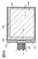
- FIG. 4A is a top view showing the light emitting device
- FIG. 4B is a cross-sectional view of FIG. 4A cut by AB and CD.
- This light emitting device includes a drive circuit unit (source line drive circuit 601), a pixel unit 602, and a drive circuit unit (gate line drive circuit 603) shown by dotted lines to control the light emission of the light emitting device.
- 604 is a sealing substrate
- 605 is a sealing material
- the inside surrounded by the sealing material 605 is a space 607.
- the routing wiring 608 is a wiring for transmitting signals input to the source line drive circuit 601 and the gate line drive circuit 603, and is a video signal, a clock signal, and a video signal and a clock signal from the FPC (flexible print circuit) 609 which is an external input terminal. Receives start signal, reset signal, etc. Although only the FPC is shown here, a printed wiring board (PWB) may be attached to the FPC.
- the light emitting device in the present specification includes not only the light emitting device main body but also a state in which an FPC or PWB is attached to the light emitting device main body.
- a drive circuit unit and a pixel unit are formed on the element substrate 610, and here, a source line drive circuit 601 which is a drive circuit unit and one pixel in the pixel unit 602 are shown.
- the element substrate 610 is manufactured by using a substrate made of glass, quartz, organic resin, metal, alloy, semiconductor, etc., as well as a plastic substrate made of FRP (Fiber Reinforced Plastics), PVF (polyvinyl fluoride), polyester, acrylic resin, etc. do it.
- FRP Fiber Reinforced Plastics
- PVF polyvinyl fluoride
- the structure of the transistor used in the pixel or the drive circuit is not particularly limited. For example, it may be an inverted stagger type transistor or a stagger type transistor. Further, a top gate type transistor or a bottom gate type transistor may be used.
- the semiconductor material used for the transistor is not particularly limited, and for example, silicon, germanium, silicon carbide, gallium nitride and the like can be used. Alternatively, an oxide semiconductor containing at least one of indium, gallium, and zinc, such as an In-Ga-Zn-based metal oxide, may be used.
- the crystallinity of the semiconductor material used for the transistor is not particularly limited, and either an amorphous semiconductor or a semiconductor having crystallinity (microcrystalline semiconductor, polycrystalline semiconductor, single crystal semiconductor, or semiconductor having a partially crystalline region). May be used. It is preferable to use a semiconductor having crystallinity because deterioration of transistor characteristics can be suppressed.
- an oxide semiconductor in addition to the transistor provided in the pixel or the drive circuit, it is preferable to apply an oxide semiconductor to a semiconductor device such as a transistor used in a touch sensor or the like described later. In particular, it is preferable to apply an oxide semiconductor having a bandgap wider than that of silicon. By using an oxide semiconductor having a bandgap wider than that of silicon, the current in the off state of the transistor can be reduced.
- the oxide semiconductor preferably contains at least indium (In) or zinc (Zn). Further, the oxide semiconductor contains an oxide represented by an In—M—Zn-based oxide (M is a metal such as Al, Ti, Ga, Ge, Y, Zr, Sn, La, Ce or Hf). Is more preferable.
- M is a metal such as Al, Ti, Ga, Ge, Y, Zr, Sn, La, Ce or Hf. Is more preferable.
- the semiconductor layer has a plurality of crystal portions, and the c-axis of the crystal portion is oriented perpendicular to the surface to be formed of the semiconductor layer or the upper surface of the semiconductor layer, and grain boundaries are formed between adjacent crystal portions. It is preferable to use an oxide semiconductor film that does not have.
- the transistor having the above-mentioned semiconductor layer can retain the electric charge accumulated in the capacitance through the transistor for a long period of time due to its low off current.
- the transistor having the above-mentioned semiconductor layer can retain the electric charge accumulated in the capacitance through the transistor for a long period of time due to its low off current.
- a base film for stabilizing the characteristics of the transistor As the base film, an inorganic insulating film such as a silicon oxide film, a silicon nitride film, a silicon nitride film, or a silicon nitride film can be used, and can be produced as a single layer or laminated.
- the base film is formed by using a sputtering method, a CVD (Chemical Vapor Deposition) method (plasma CVD method, thermal CVD method, MOCVD (Metal Organic CVD) method, etc.), ALD (Atomic Layer Deposition) method, coating method, printing method, etc. can.
- the base film may not be provided if it is not necessary.
- the FET 623 represents one of the transistors formed in the source line drive circuit 601.
- the drive circuit may be formed of various CMOS circuits, epitaxial circuits or NMOS circuits.
- the driver integrated type in which the drive circuit is formed on the substrate is shown, but it is not always necessary, and the drive circuit can be formed on the outside instead of on the substrate.
- the pixel unit 602 is formed by a plurality of pixels including a switching FET 611, a current control FET 612, and a first electrode 613 electrically connected to the drain thereof, but the pixel portion 602 is not limited to 3
- a pixel unit may be a combination of two or more FETs and a capacitive element.
- An insulator 614 is formed so as to cover the end portion of the first electrode 613.
- it can be formed by using a positive photosensitive acrylic resin film.
- a curved surface having a curvature is formed at the upper end portion or the lower end portion of the insulating material 614.
- a positive photosensitive acrylic resin is used as the material of the insulating material 614
- a negative type photosensitive resin or a positive type photosensitive resin can be used as the insulating material 614.
- An EL layer 616 and a second electrode 617 are formed on the first electrode 613, respectively.
- the material used for the first electrode 613 that functions as an anode it is desirable to use a material having a large work function.
- a single layer such as an ITO film, an indium tin oxide film containing silicon, an indium oxide film containing 2 wt% or more and 20 wt% or less of zinc oxide, a titanium nitride film, a chromium film, a tungsten film, a Zn film, or a Pt film.
- a laminated structure of a titanium nitride film and a film containing aluminum as a main component a three-layer structure of a titanium nitride film, a film containing aluminum as a main component, and a titanium nitride film can be used.
- the resistance as wiring is low, good ohmic contact can be obtained, and the structure can further function as an anode.
- the EL layer 616 is formed by various methods such as a thin-film deposition method using a thin-film deposition mask, an inkjet method, and a spin coating method.
- the EL layer 616 includes a configuration as described in any one of the first to fourth embodiments.
- the other material constituting the EL layer 616 may be a low molecular weight compound or a high molecular weight compound (including an oligomer and a dendrimer).
- the material used for the second electrode 617 formed on the EL layer 616 and functioning as a cathode a material having a small work function (Al, Mg, Li, Ca, or an alloy or compound thereof (MgAg, MgIn, etc.) It is preferable to use AlLi etc.)).
- the second electrode 617 is a thin metal thin film and a transparent conductive film (ITO, 2 wt% or more and 20 wt% or less). It is preferable to use a laminate with indium oxide containing zinc oxide, indium tin oxide containing silicon, zinc oxide (ZnO), etc.).
- a light emitting device is formed by the first electrode 613, the EL layer 616, and the second electrode 617.
- the light emitting device is the light emitting device according to any one of the first to fourth embodiments.
- a plurality of light emitting devices are formed in the pixel portion, and the light emitting device according to the present embodiment has the light emitting device according to any one of the first to fourth embodiments and other configurations. Both light emitting devices may be mixed.
- the sealing substrate 604 by bonding the sealing substrate 604 to the element substrate 610 with the sealing material 605, the light emitting device 618 is provided in the space 607 surrounded by the element substrate 610, the sealing substrate 604, and the sealing material 605.
- the space 607 is filled with a filler, which may be filled with an inert gas (nitrogen, argon, etc.) or a sealing material.
- an epoxy resin or a glass frit for the sealing material 605. Further, it is desirable that these materials are materials that do not allow moisture and oxygen to permeate as much as possible. Further, as a material used for the sealing substrate 604, in addition to a glass substrate or a quartz substrate, a plastic substrate made of FRP (Fiber Reinforced Plastics), PVF (polyvinyl fluoride), polyester, acrylic resin or the like can be used.
- FRP Fiber Reinforced Plastics
- PVF polyvinyl fluoride
- polyester acrylic resin or the like
- a protective film may be provided on the second electrode.
- the protective film may be formed of an organic resin film or an inorganic insulating film. Further, a protective film may be formed so as to cover the exposed portion of the sealing material 605. Further, the protective film can be provided so as to cover the surface and side surfaces of the pair of substrates, the sealing layer, the insulating layer, and the exposed side surfaces.
- the protective film a material that does not easily allow impurities such as water to permeate can be used. Therefore, it is possible to effectively prevent impurities such as water from diffusing from the outside to the inside.
- oxides, nitrides, fluorides, sulfides, ternary compounds, metals, polymers and the like can be used, and for example, aluminum oxide, hafnium oxide, hafnium silicate, lanthanum oxide, and oxidation.
- the protective film is preferably formed by using a film forming method having good step coverage (step coverage).
- a film forming method having good step coverage is the atomic layer deposition (ALD) method.
- ALD atomic layer deposition
- ALD method it is possible to form a protective film having a dense, reduced defects such as cracks or pinholes, or a uniform thickness.
- damage to the processed member when forming the protective film can be reduced.
- the protective film by using the ALD method, it is possible to form a protective film having a complicated uneven shape or a uniform and few defects on the upper surface, the side surface and the back surface of the touch panel.
- a light emitting device manufactured by using the light emitting device according to any one of the first to fourth embodiments can be obtained.
- the light emitting device according to the present embodiment uses the light emitting device according to any one of the first to fourth embodiments, it is possible to obtain a light emitting device having good characteristics. Specifically, since the light emitting device according to any one of the first to fourth embodiments has good luminous efficiency, it can be a light emitting device having low power consumption.
- FIG. 5 shows an example of a light emitting device in which a light emitting device exhibiting white light emission is formed and a colored layer (color filter) or the like is provided to make the light emitting device full color.
- FIG. 5A shows a substrate 1001, an underlying insulating film 1002, a gate insulating film 1003, a gate electrode 1006, 1007, 1008, a first interlayer insulating film 1020, a second interlayer insulating film 1021, a peripheral portion 1042, a pixel portion 1040, and a drive.
- the circuit unit 1041, the first electrode of the light emitting device 1024W, 1024R, 1024G, 1024B, the partition wall 1025, the EL layer 1028, the second electrode 1029 of the light emitting device, the sealing substrate 1031, the sealing material 1032, and the like are shown.
- the colored layer (red colored layer 1034R, green colored layer 1034G, blue colored layer 1034B) is provided on the transparent base material 1033. Further, a black matrix 1035 may be further provided. The transparent substrate 1033 provided with the colored layer and the black matrix is aligned and fixed to the substrate 1001. The colored layer and the black matrix 1035 are covered with the overcoat layer 1036. Further, in FIG. 5A, there is a light emitting layer in which light is emitted to the outside without passing through the colored layer and a light emitting layer in which light is transmitted through the colored layer of each color and emitted to the outside. Since the light transmitted through the white and colored layers is red, green, and blue, an image can be expressed by pixels of four colors.
- FIG. 5B shows an example in which a colored layer (red colored layer 1034R, green colored layer 1034G, blue colored layer 1034B) is formed between the gate insulating film 1003 and the first interlayer insulating film 1020.
- the colored layer may be provided between the substrate 1001 and the sealing substrate 1031.
- the light emitting device has a structure that extracts light to the substrate 1001 side on which the FET is formed (bottom emission type), but has a structure that extracts light to the sealing substrate 1031 side (top emission type). ) May be used as a light emitting device.
- a cross-sectional view of the top emission type light emitting device is shown in FIG.
- the substrate 1001 can be a substrate that does not allow light to pass through. It is formed in the same manner as the bottom emission type light emitting device until the connection electrode for connecting the FET and the anode of the light emitting device is manufactured.
- a third interlayer insulating film 1037 is formed so as to cover the electrode 1022. This insulating film may play a role of flattening.
- the third interlayer insulating film 1037 can be formed by using the same material as the second interlayer insulating film and other known materials.
- the first electrodes 1024W, 1024R, 1024G, and 1024B of the light emitting device are used as anodes here, but may be cathodes. Further, in the case of the top emission type light emitting device as shown in FIG. 6, it is preferable that the first electrode is a reflecting electrode.
- the structure of the EL layer 1028 is the same as that described as the unit 103 in any one of the first to fourth embodiments, and the element structure is such that white light emission can be obtained.
- sealing can be performed by the sealing substrate 1031 provided with the colored layers (red colored layer 1034R, green colored layer 1034G, blue colored layer 1034B).
- the sealing substrate 1031 may be provided with a black matrix 1035 so as to be located between the pixels.
- the colored layer (red colored layer 1034R, green colored layer 1034G, blue colored layer 1034B) or black matrix may be covered by the overcoat layer 1036.
- a substrate having translucency is used as the sealing substrate 1031.
- an example of performing full-color display with four colors of red, green, blue, and white is shown, but the present invention is not particularly limited, and full-color with four colors of red, yellow, green, and blue, or three colors of red, green, and blue. It may be displayed.
- the microcavity structure can be preferably applied.
- a light emitting device having a microcavity structure can be obtained by using a first electrode as a reflective electrode and a second electrode as a semitransmissive / semireflective electrode.
- An EL layer is provided between the reflective electrode and the semi-transmissive / semi-reflective electrode, and at least a light emitting layer serving as a light emitting region is provided.
- the reflecting electrode is a film having a visible light reflectance of 40% to 100%, preferably 70% to 100%, and a resistivity of 1 ⁇ 10-2 ⁇ cm or less.
- the semi-transmissive / semi-reflective electrode is a film having a visible light reflectance of 20% to 80%, preferably 40% to 70%, and a resistivity of 1 ⁇ 10-2 ⁇ cm or less. ..
- the light emitted from the light emitting layer included in the EL layer is reflected by the reflecting electrode and the semitransparent / semi-reflecting electrode and resonates.
- the light emitting device can change the optical distance between the reflective electrode and the semi-transmissive / semi-reflective electrode by changing the thickness of the transparent conductive film, the above-mentioned composite material, the carrier transport material, or the like. As a result, it is possible to intensify the light having a wavelength that resonates between the reflective electrode and the semi-transmissive / semi-reflective electrode, and to attenuate the light having a wavelength that does not resonate.
- the light reflected by the reflecting electrode and returned causes a large interference with the light directly incident on the semitransparent / semi-reflecting electrode from the light emitting layer (first incident light), and is therefore reflected.
- the EL layer may have a structure having a plurality of light emitting layers or a structure having a single light emitting layer.
- the tandem type light emitting device in combination with the above-mentioned configuration of the tandem type light emitting device, one It may be applied to a configuration in which a plurality of EL layers are provided on one light emitting device with a charge generation layer interposed therebetween, and a single or a plurality of light emitting layers are formed on each EL layer.
- microcavity structure By having the microcavity structure, it is possible to enhance the emission intensity in the front direction of a specific wavelength, so that it is possible to reduce power consumption.
- a microcavity structure that matches the wavelength of each color to all sub-pixels in addition to the effect of improving brightness by emitting yellow light. It can be a light emitting device having good characteristics.
- the light emitting device according to the present embodiment uses the light emitting device according to any one of the first to fourth embodiments, it is possible to obtain a light emitting device having good characteristics. Specifically, since the light emitting device according to any one of the first to fourth embodiments has good luminous efficiency, it can be a light emitting device having low power consumption.
- FIG. 7 shows a passive matrix type light emitting device manufactured by applying the present invention.
- 7A is a perspective view showing the light emitting device
- FIG. 7B is a cross-sectional view of FIG. 7A cut by XY.
- an EL layer 955 is provided between the electrodes 952 and the electrodes 956 on the substrate 951.
- the end of the electrode 952 is covered with an insulating layer 953.
- a partition layer 954 is provided on the insulating layer 953.
- the side wall of the partition wall layer 954 has an inclination such that the distance between one side wall and the other side wall becomes narrower as it gets closer to the substrate surface. That is, the cross section in the short side direction of the partition wall layer 954 is trapezoidal, and the bottom side (the side facing the same direction as the surface direction of the insulating layer 953 and in contact with the insulating layer 953) is the upper side (the surface of the insulating layer 953). It faces in the same direction as the direction, and is shorter than the side that does not contact the insulating layer 953).
- the partition wall layer 954 in this way, it is possible to prevent defects in the light emitting device due to static electricity or the like.
- the light emitting device according to any one of the first to fourth embodiments is used, and the light emitting device has good reliability or low power consumption. can do.
- the light emitting device described above can control a large number of minute light emitting devices arranged in a matrix, it is a light emitting device that can be suitably used as a display device for expressing an image.
- FIG. 8B is a top view of the lighting device
- FIG. 8A is a cross-sectional view taken along the line ef in FIG. 8B.
- the first electrode 401 is formed on the translucent substrate 400 which is a support.
- the first electrode 401 corresponds to the electrode 101 in any one of the first to fourth embodiments.
- the first electrode 401 is formed of a translucent material.
- a pad 412 for supplying a voltage to the second electrode 404 is formed on the substrate 400.
- the EL layer 403 is formed on the first electrode 401.
- the EL layer 403 corresponds to the configuration of the unit 103 in any one of the first to fourth embodiments, or the combined configuration of the unit 103 (2), the layer 104, the layer 105, and the intermediate layer 106. Please refer to the description for these configurations.
- the EL layer 403 is covered to form the second electrode 404.
- the second electrode 404 corresponds to the electrode 102 in any one of the first to fourth embodiments.
- the second electrode 404 is formed of a material having high reflectance. A voltage is supplied by connecting the second electrode 404 to the pad 412.
- the lighting device showing the light emitting device having the first electrode 401, the EL layer 403, and the second electrode 404 in the present embodiment has. Since the light emitting device is a light emitting device having high luminous efficiency, the lighting device in the present embodiment can be a lighting device having low power consumption.
- the illumination device is completed by fixing the substrate 400 on which the light emitting device having the above configuration is formed and the sealing substrate 407 using the sealing materials 405 and 406 and sealing them. Either one of the sealing materials 405 and 406 may be used. Further, a desiccant can be mixed with the inner sealing material 406 (not shown in FIG. 8B), whereby moisture can be adsorbed, which leads to improvement in reliability.
- an IC chip 420 or the like on which a converter or the like is mounted may be provided on the IC chip 420.
- the lighting device according to the present embodiment uses the light emitting device according to any one of the first to fourth embodiments for the EL element, and can be a lighting device having low power consumption. ..
- the light emitting device according to any one of the first to fourth embodiments is a light emitting device having good luminous efficiency and low power consumption.
- the electronic device described in the present embodiment can be an electronic device having a light emitting unit having low power consumption.
- Examples of electronic devices to which the above light emitting device is applied include television devices (also referred to as televisions or television receivers), monitors for computers, digital cameras, digital video cameras, digital photo frames, mobile phones (mobile phones, etc.). (Also referred to as a mobile phone device), a portable game machine, a mobile information terminal, a sound reproduction device, a large game machine such as a pachinko machine, and the like. Specific examples of these electronic devices are shown below.
- FIG. 9A shows an example of a television device.
- the display unit 7103 is incorporated in the housing 7101. Further, here, a configuration in which the housing 7101 is supported by the stand 7105 is shown. An image can be displayed by the display unit 7103, and the display unit 7103 is configured by arranging the light emitting devices according to any one of the first to fourth embodiments in a matrix.
- the operation of the television device can be performed by an operation switch provided in the housing 7101 or a separate remote control operation device 7110.
- the operation keys 7109 included in the remote controller 7110 can be used to operate the channel or volume, and the image displayed on the display unit 7103 can be operated.
- the remote controller 7110 may be provided with a display unit 7107 for displaying information output from the remote controller 7110.
- the television device is configured to include a receiver, a modem, and the like.
- the receiver can receive general television broadcasts, and by connecting to a wired or wireless communication network via a modem, it can be unidirectional (sender to receiver) or bidirectional (sender and receiver). It is also possible to perform information communication between (or between recipients, etc.).
- FIG. 9B is a computer, which includes a main body 7201, a housing 7202, a display unit 7203, a keyboard 7204, an external connection port 7205, a pointing device 7206, and the like.
- This computer is manufactured by arranging the light emitting devices according to any one of the first to fourth embodiments in a matrix and using them in the display unit 7203.
- the computer of FIG. 9B may have the form shown in FIG. 9C.
- the computer of FIG. 9C is provided with a second display unit 7210 instead of the keyboard 7204 and the pointing device 7206.
- the second display unit 7210 is a touch panel type, and input can be performed by operating the input display displayed on the second display unit 7210 with a finger or a dedicated pen.
- the second display unit 7210 can display not only the input display but also other images. Further, the display unit 7203 may also be a touch panel. By connecting the two screens with a hinge, it is possible to prevent troubles such as damage or damage to the screens during storage or transportation.
- FIG. 9D shows an example of a mobile terminal.
- the mobile phone includes an operation button 7403, an external connection port 7404, a speaker 7405, a microphone 7406, and the like, in addition to the display unit 7402 incorporated in the housing 7401.
- the mobile phone has a display unit 7402 manufactured by arranging the light emitting devices according to any one of the first to fourth embodiments in a matrix.
- the mobile terminal shown in FIG. 9D may be configured so that information can be input by touching the display unit 7402 with a finger or the like. In this case, operations such as making a phone call or composing an e-mail can be performed by touching the display unit 7402 with a finger or the like.
- the screen of the display unit 7402 mainly has three modes. The first is a display mode mainly for displaying an image, and the second is an input mode mainly for inputting information such as characters. The third is a display + input mode in which two modes, a display mode and an input mode, are mixed.
- the display unit 7402 may be set to a character input mode mainly for inputting characters, and the characters displayed on the screen may be input. In this case, it is preferable to display the keyboard or the number button on most of the screen of the display unit 7402.
- the orientation (vertical or horizontal) of the mobile terminal is determined, and the screen display of the display unit 7402 is automatically displayed. Can be switched.
- the screen mode can be switched by touching the display unit 7402 or by operating the operation button 7403 of the housing 7401. It is also possible to switch depending on the type of image displayed on the display unit 7402. For example, if the image signal displayed on the display unit is moving image data, the display mode is switched, and if the image signal is text data, the input mode is switched.
- the input mode the signal detected by the optical sensor of the display unit 7402 is detected, and when there is no input by the touch operation of the display unit 7402 for a certain period of time, the screen mode is switched from the input mode to the display mode. You may control it.
- the display unit 7402 can also function as an image sensor.
- the person can be authenticated by touching the display unit 7402 with a palm or a finger and imaging a palm print, a fingerprint, or the like.
- a backlight that emits near-infrared light or a sensing light source that emits near-infrared light is used for the display unit, finger veins, palmar veins, and the like can be imaged.
- FIG. 10A is a schematic view showing an example of a cleaning robot.
- the cleaning robot 5100 has a display 5101 arranged on the upper surface, a plurality of cameras 5102 arranged on the side surface, a brush 5103, and an operation button 5104. Although not shown, the lower surface of the cleaning robot 5100 is provided with tires, suction ports, and the like.
- the cleaning robot 5100 also includes various sensors such as an infrared sensor, an ultrasonic sensor, an acceleration sensor, a piezo sensor, an optical sensor, and a gyro sensor. Further, the cleaning robot 5100 is provided with wireless communication means.
- the cleaning robot 5100 is self-propelled, can detect dust 5120, and can suck dust from a suction port provided on the lower surface.
- the cleaning robot 5100 can analyze the image taken by the camera 5102 and determine the presence or absence of obstacles such as walls, furniture, and steps. Further, when an object such as wiring that is likely to be entangled with the brush 5103 is detected by image analysis, the rotation of the brush 5103 can be stopped.
- the display 5101 can display the remaining amount of the battery, the amount of dust sucked, and the like.
- the route traveled by the cleaning robot 5100 may be displayed on the display 5101. Further, the display 5101 may be a touch panel, and the operation buttons 5104 may be provided on the display 5101.
- the cleaning robot 5100 can communicate with a portable electronic device 5140 such as a smartphone.
- the image taken by the camera 5102 can be displayed on the portable electronic device 5140. Therefore, the owner of the cleaning robot 5100 can know the state of the room even when he / she is out. Further, the display of the display 5101 can be confirmed by a portable electronic device 5140 such as a smartphone.
- the light emitting device of one aspect of the present invention can be used for the display 5101.
- the robot 2100 shown in FIG. 10B includes a computing device 2110, an illuminance sensor 2101, a microphone 2102, an upper camera 2103, a speaker 2104, a display 2105, a lower camera 2106, an obstacle sensor 2107, and a moving mechanism 2108.
- the microphone 2102 has a function of detecting a user's voice, environmental sound, and the like. Further, the speaker 2104 has a function of emitting sound.
- the robot 2100 can communicate with the user using the microphone 2102 and the speaker 2104.
- the display 2105 has a function of displaying various information.
- the robot 2100 can display the information desired by the user on the display 2105.
- the display 2105 may be equipped with a touch panel. Further, the display 2105 may be a removable information terminal, and by installing the display 2105 at a fixed position of the robot 2100, charging and data transfer are possible.
- the upper camera 2103 and the lower camera 2106 have a function of photographing the surroundings of the robot 2100. Further, the obstacle sensor 2107 can detect the presence or absence of an obstacle in the traveling direction when the robot 2100 advances by using the moving mechanism 2108. The robot 2100 can recognize the surrounding environment and move safely by using the upper camera 2103, the lower camera 2106, and the obstacle sensor 2107.
- the light emitting device of one aspect of the present invention can be used for the display 2105.
- FIG. 10C is a diagram showing an example of a goggle type display.
- the goggle type display includes, for example, a housing 5000, a display unit 5001, a speaker 5003, an LED lamp 5004, a connection terminal 5006, and a sensor 5007 (force, displacement, position, speed, acceleration, angular speed, rotation speed, distance, light, liquid, etc. Includes functions to measure magnetism, temperature, chemicals, voice, time, hardness, electric field, current, voltage, power, radiation, flow rate, humidity, gradient, vibration, odor, or infrared rays), microphone 5008, display 5002 , Support portion 5012, earphone 5013, and the like.
- the light emitting device of one aspect of the present invention can be used for the display unit 5001 and the display unit 5002.
- FIG. 11 shows an example in which the light emitting device according to any one of the first to fourth embodiments is used for a desk lamp which is a lighting device.
- the desk lamp shown in FIG. 11 has a housing 2001 and a light source 2002, and the lighting device according to the sixth embodiment may be used as the light source 2002.
- FIG. 12 is an example in which the light emitting device according to any one of the first to fourth embodiments is used as the indoor lighting device 3001. Since the light emitting device according to any one of the first to fourth embodiments is a light emitting device having high luminous efficiency, it can be a lighting device having low power consumption. Further, since the light emitting device according to any one of the first to fourth embodiments can have a large area, it can be used as a lighting device having a large area. Further, since the light emitting device according to any one of the first to fourth embodiments is thin, it can be used as a thin lighting device.
- the light emitting device according to any one of the first to fourth embodiments can also be mounted on the windshield or dashboard of an automobile.
- FIG. 13 shows an embodiment in which the light emitting device according to any one of the first to fourth embodiments is used for a windshield or a dashboard of an automobile.
- the display area 5200 to the display area 5203 is a display area provided by using the light emitting device according to any one of the first to fourth embodiments.
- the display area 5200 and the display area 5201 are display devices equipped with the light emitting device according to any one of the first to fourth embodiments provided on the windshield of the automobile.
- the first electrode and the second electrode are made of translucent electrodes so that the opposite side can be seen through, so-called see-through. It can be a status display device. If the display is in a see-through state, even if it is installed on the windshield of an automobile, it can be installed without obstructing the view.
- a transistor for driving it is preferable to use a transistor having translucency, such as an organic transistor made of an organic semiconductor material or a transistor using an oxide semiconductor.
- the display area 5202 is a display device provided with the light emitting device according to any one of the first to fourth embodiments provided in the pillar portion.
- the display area 5203 provided on the dashboard portion compensates for the blind spot and enhances safety by projecting an image from an imaging means provided on the outside of the automobile from the field of view blocked by the vehicle body. Can be done. By projecting the image so as to complement the invisible part, it is possible to confirm the safety more naturally and without discomfort.
- the display area 5203 can provide various information by displaying navigation information, speed or rotation, mileage, remaining fuel amount, gear state, air conditioning setting, and the like.
- the display items or layout of the display can be changed as appropriate according to the preference of the user. It should be noted that such information can also be provided in the display area 5200 to the display area 5202. Further, the display area 5200 to the display area 5203 can also be used as a lighting device.
- FIGS. 14A to 14C show a foldable portable information terminal 9310.
- FIG. 14A shows the mobile information terminal 9310 in the expanded state.
- FIG. 14B shows a mobile information terminal 9310 in a state of being changed from one of the expanded state or the folded state to the other.
- FIG. 14C shows a mobile information terminal 9310 in a folded state.
- the mobile information terminal 9310 is excellent in portability in the folded state, and is excellent in display listability due to a wide seamless display area in the unfolded state.
- the display panel 9311 is supported by three housings 9315 connected by hinges 9313.
- the display panel 9311 may be a touch panel (input / output device) equipped with a touch sensor (input device). Further, the display panel 9311 can be reversibly deformed from the unfolded state to the folded state of the portable information terminal 9310 by bending between the two housings 9315 via the hinge 9313.
- the light emitting device of one aspect of the present invention can be used for the display panel 9311.
- the configurations shown in the present embodiment can be used by appropriately combining the configurations shown in the first to fourth embodiments.
- the range of application of the light emitting device provided with the light emitting device according to any one of the first to fourth embodiments is extremely wide, and the light emitting device can be applied to electronic devices in all fields. be.
- an electronic device having low power consumption can be obtained.
- 15A and 15B are cross-sectional views illustrating the configuration of the manufactured light emitting device.
- FIG. 16 is a diagram for explaining the current density-luminance characteristic of the light emitting device 1.
- FIG. 17 is a diagram illustrating a luminance-current efficiency characteristic of the light emitting device 1.
- FIG. 18 is a diagram illustrating a voltage-luminance characteristic of the light emitting device 1.
- FIG. 19 is a diagram illustrating a voltage-current characteristic of the light emitting device 1.
- FIG. 20 is a diagram illustrating a luminance-external quantum efficiency characteristic of the light emitting device 1.
- the external quantum efficiency was calculated from the brightness and emission spectrum observed from the front, assuming that the light distribution characteristics of the light emitting device are Lambertian type.
- FIG. 21 is a diagram illustrating an emission spectrum when the light emitting device 1 is made to emit light at a brightness of 1000 cd / m 2.
- FIG. 22 is a diagram for explaining the normalized luminance-time change characteristic when the light emitting device 1 is made to emit light at a constant current density of 50 mA / cm 2.
- the normalized luminance-time change characteristic when the comparative light emitting device is made to emit light at a constant current density of 50 mA / cm 2 is also shown.
- FIG. 23 is a diagram for explaining the current density-luminance characteristic of the light emitting device 2.
- FIG. 24 is a diagram illustrating a luminance-current efficiency characteristic of the light emitting device 2.
- FIG. 25 is a diagram for explaining the voltage-luminance characteristic of the light emitting device 2.
- FIG. 26 is a diagram illustrating a voltage-current characteristic of the light emitting device 2.
- FIG. 27 is a diagram illustrating a luminance-external quantum efficiency characteristic of the light emitting device 2.
- the external quantum efficiency was calculated from the brightness and emission spectrum observed from the front, assuming that the light distribution characteristics of the light emitting device are Lambertian type.
- FIG. 28 is a diagram illustrating an emission spectrum when the light emitting device 2 is made to emit light at a brightness of 1000 cd / m 2.
- FIG. 29 is a diagram for explaining the normalized luminance-time change characteristic when the light emitting device 2 is made to emit light at a constant current density of 50 mA / cm 2.
- the normalized luminance-time change characteristic when the comparative light emitting device is made to emit light at a constant current density of 50 mA / cm 2 is also shown.
- FIG. 30 is a diagram for explaining the current density-luminance characteristic of the light emitting device 3.
- FIG. 31 is a diagram illustrating a luminance-current efficiency characteristic of the light emitting device 3.
- FIG. 32 is a diagram for explaining the voltage-luminance characteristic of the light emitting device 3.
- FIG. 33 is a diagram illustrating a voltage-current characteristic of the light emitting device 3.
- FIG. 34 is a diagram illustrating the luminance-external quantum efficiency characteristics of the light emitting device 3.
- the external quantum efficiency was calculated from the brightness and emission spectrum observed from the front, assuming that the light distribution characteristics of the light emitting device are Lambertian type.
- FIG. 35 is a diagram illustrating an emission spectrum when the light emitting device 3 is made to emit light at a brightness of 1000 cd / m 2.
- FIG. 36 is a diagram illustrating a normalized luminance-time change characteristic when the light emitting device 3 is made to emit light at a constant current density of 50 mA / cm 2.
- the normalized luminance-time change characteristic when the comparative light emitting device is made to emit light at a constant current density of 50 mA / cm 2 is also shown.
- FIG. 37 is a diagram illustrating a current density-luminance characteristic of the light emitting device 4.
- FIG. 38 is a diagram illustrating a luminance-current efficiency characteristic of the light emitting device 4.
- FIG. 39 is a diagram illustrating a voltage-luminance characteristic of the light emitting device 4.
- FIG. 40 is a diagram illustrating a voltage-current characteristic of the light emitting device 4.
- FIG. 41 is a diagram illustrating a luminance-external quantum efficiency characteristic of the light emitting device 4.
- the external quantum efficiency was calculated from the brightness and emission spectrum observed from the front, assuming that the light distribution characteristics of the light emitting device are Lambertian type.
- FIG. 42 is a diagram illustrating an emission spectrum when the light emitting device 4 is made to emit light at a brightness of 1000 cd / m 2.
- FIG. 43 is a diagram for explaining the normalized luminance-time change characteristic when the light emitting device 4 is made to emit light at a constant current density of 50 mA / cm 2.
- the normalized luminance-time change characteristic when the comparative light emitting device is made to emit light at a constant current density of 50 mA / cm 2 is also shown.
- 44A and 44B are cross-sectional views illustrating the configuration of the manufactured light emitting device.
- FIG. 45 is a diagram illustrating a current density-luminance characteristic of the light emitting device 5.
- FIG. 46 is a diagram illustrating a luminance-current efficiency characteristic of the light emitting device 5.
- FIG. 47 is a diagram illustrating a voltage-luminance characteristic of the light emitting device 5.
- FIG. 48 is a diagram illustrating a voltage-current characteristic of the light emitting device 5.
- FIG. 49 is a diagram illustrating a luminance-external quantum efficiency characteristic of the light emitting device 5.
- the external quantum efficiency was calculated from the brightness and emission spectrum observed from the front, assuming that the light distribution characteristics of the light emitting device are Lambertian type.
- FIG. 50 is a diagram illustrating an emission spectrum when the light emitting device 5 is made to emit light at a brightness of 1000 cd / m 2.
- FIG. 51 is a diagram illustrating a normalized luminance-time change characteristic when the light emitting device 5 is made to emit light at a constant current density of 50 mA / cm 2.
- the normalized luminance-time change characteristic when the comparative light emitting device is made to emit light at a constant current density of 50 mA / cm 2 is also shown.
- the manufactured light emitting device 1 described in this embodiment has the same configuration as the light emitting device 150 (see FIG. 15A).
- the light emitting device 150 includes an electrode 101, an electrode 102, a unit 103, and a layer 104, and the electrode 102 includes a region overlapping the electrode 101.
- the unit 103 includes a region sandwiched between the electrodes 101 and 102, and the unit 103 includes layers 111 and 112.
- the layer 111 includes a region sandwiching the layer 112 with the electrode 101, and the layer 111 contains a luminescent material EM.
- EM luminescent material
- the layer 104 comprises a region sandwiched between the layer 112 and the electrode 101, the layer 104 comprises a material AM and a material HT1 having acceptability, and the layer 104 comprises a region 104A and a region 104B.
- an electron acceptor material abbreviation: OCHD-001
- BBABnf was used as the material HT1.
- the region 104A comprises a region sandwiched between the region 104B and the electrode 101, the region 104A contains a material AM having an acceptability at a concentration C1, and a region 104B contains a material AM having an acceptability at a concentration C2.
- the concentration C2 is higher than zero and lower than the concentration C1.
- region 104A was formed using only OCHD-001, and 104B was formed using BBABnf and OCHD-001.
- the layer 112 comprises a region 112A and a region 112B, the region 112B comprises a region sandwiched between the layer 111 and the region 112A, and the region 112B contains the material HT2.
- PCzN2 was used as the material HT2.
- the material HT1 had a first HOMO level, and the first HOMO level was ⁇ 5.7 eV or more and ⁇ 5.4 eV or less. According to cyclic voltammetry (CV) measurement, the HOMO level of BBABnf was ⁇ 5.56 eV.
- the material HT2 had a second HOMO level, and the second HOMO level was in the range of ⁇ 0.2 eV or more and 0 eV or less with respect to the first HOMO level. According to the CV measurement, the HOMO level of PCzN2 was ⁇ 5.71 eV.
- the layer 113 includes a region sandwiched between the electrode 102 and the layer 111, the layer 113 includes a material OMC, and the material OMC is an organic complex of an alkali metal or an organic complex of an alkaline earth metal.
- the material OMC is an organic complex of an alkali metal or an organic complex of an alkaline earth metal.
- Liq was used as the material OMC.
- Layer 111 comprises a host material HOST, the host material HOST comprising a first LUMO level.
- the host material HOST comprising a first LUMO level.
- ⁇ N- ⁇ NPAnth was used as the host material HOST.
- the LUMO level of ⁇ N- ⁇ NPAnth was -2.74 eV.
- the unit 103 comprises a layer 113, the layer 113 comprising a region 113A and a region 113B, and the region 113A comprising a region sandwiched between the regions 113B and 111.
- Region 113A contains material ET and region 113B contains material OMC.
- the material ET comprises a second LUMO level.
- ZADN was used as the material ET.
- the LUMO level of ZADN was -2.87 eV. Therefore, the second LUMO level is in the range of ⁇ 0.4 eV or more and ⁇ 0.11 eV or less with respect to the first LUMO level.
- region 104A is in contact with the electrode 101.
- Configuration of light emitting device 1 The configuration of the light emitting device 1 is shown in Table 1. Further, the structural formula of the material used for the light emitting device described in this embodiment is shown below.
- An electrochemical analyzer (manufactured by BAS Co., Ltd., model number: ALS model 600A or 600C) was used as the measuring device.
- dehydrated dimethylformamide (DMF) (manufactured by Aldrich Co., Ltd., 99.8%, catalog number; 22705-6) was used as a solvent, and tetra-n-butylammonium perchlorate (supporting electrolyte) was used.
- n-Bu 4 NCLO 4 manufactured by Tokyo Kasei Co., Ltd., catalog number; T0836
- a platinum electrode (manufactured by BAS Co., Ltd., PTE platinum electrode) is used as the working electrode, and a platinum electrode (manufactured by BAS Co., Ltd., Pt counter electrode for VC-3) is used as the auxiliary electrode. 5 cm)) was used as a reference electrode, and an Ag / Ag + electrode (RE7 non-aqueous solvent system reference electrode manufactured by BAS Co., Ltd.) was used. The measurement was performed at room temperature (20 or more and 25 ° C. or less).
- the scan speed at the time of CV measurement was unified to 0.1 V / sec, and the oxidation potential Ea [V] and the reduction potential Ec [V] with respect to the reference electrode were measured.
- Ea was the intermediate potential of the oxidation-reduction wave
- Ec was the intermediate potential of the reduction-oxidation wave.
- the potential energy of the reference electrode used in this embodiment with respect to the vacuum level is known to be -4.94 [eV]
- the HOMO level [eV] -4.94-Ea, LUMO.
- the light emitting device 1 described in this example was produced by using a method having the following steps.
- the electrode 101 was formed. Specifically, it was formed by a sputtering method using indium-tin oxide (abbreviation: ITSO) containing silicon or silicon oxide as a target.
- ITSO indium-tin oxide
- the electrode 101 includes ITSO, has a thickness of 70 nm, and has an area of 4 mm 2 (2 mm ⁇ 2 mm).
- the base material on which the electrode 101 was formed was washed with water, fired at 200 ° C. for 1 hour, and then subjected to UV ozone treatment for 370 seconds.
- the substrate was introduced into a vacuum vapor deposition apparatus whose internal pressure was reduced to about 10-4 Pa, and vacuum firing was performed at 170 ° C. for 30 minutes in a heating chamber inside the vacuum vapor deposition apparatus. Then, the substrate was allowed to cool for about 30 minutes.
- a region 104A was formed on the electrode 101. Specifically, the pressure inside the vacuum deposition apparatus was reduced to 10 -4 Pa, and then the material was vapor-deposited using a resistance heating method.
- the region 104A includes OCHD-001 and has a thickness of 1 nm.
- a region 104B was formed on the region 104A. Specifically, the material was co-deposited using a resistance heating method.
- a region 112A was formed on the region 104B. Specifically, the material was vapor-deposited using the resistance heating method.
- the region 112A contains BBABnf and has a thickness of 20 nm.
- the region 112B was formed on the region 112A. Specifically, the material was vapor-deposited using the resistance heating method.
- the region 112B contains 3,3'-(naphthalene-1,4-diyl) bis (9-phenyl-9H-carbazole) (abbreviation: PCzN2) and has a thickness of 10 nm.
- layer 111 was formed on region 112B. Specifically, the material was co-deposited using a resistance heating method.
- region 113A was formed on layer 111. Specifically, the material was co-deposited using a resistance heating method.
- ZADN 2- ⁇ 4- [9,10-di (naphthalene-2-yl) -2-anthryl] phenyl ⁇ -1-phenyl-1H-benzimidazole
- the region 113B was formed on the region 113A. Specifically, the material was co-deposited using a resistance heating method.
- the electrode 102 was formed on the region 113B. Specifically, the material was vapor-deposited using the resistance heating method.
- the electrode 102 contains Al and has a thickness of 120 nm.
- Table 2 shows the main initial expectations when the light emitting device 1 is made to emit light at a brightness of about 1000 cd / m 2. (Note that the initial characteristics of other light emitting devices are also described in Table 2, and the configuration thereof will be described later. do).
- the light emitting device 1 was found to exhibit good characteristics. For example, the voltage required to emit light at a brightness of 1000 cd / m 2 was lower than that of the comparative light emitting device 1A. Further, when the light emitting device 1 was continuously made to emit light at a constant current density of 50 mA / cm 2 , the decrease in brightness was small as compared with the comparative light emitting device 1A (see FIG. 22). Specifically, the decrease in brightness was improved after about 525 hours. For example, in about 940 hours, the characteristic of decreasing to 92.1% of the initial brightness was improved to 93.6% of the initial brightness. As a result, reliability can be improved while suppressing the drive voltage. As a result, it has been possible to provide a new light emitting device having excellent convenience, usefulness or reliability.
- ⁇ Light emitting device 2> The configuration of the light emitting device 2 is shown in Table 3.
- the concentration of the material AM having acceptability contained in the region 104B is lower than that of the light emitting device 1.
- the region 104B of the light emitting device 1 contains OCHD-001 at a concentration of 0.10 with respect to BBABnf
- the region 104B of the light emitting device 2 contains OCHD-001 at a concentration of 0.03 with respect to BBABnf.
- the different parts will be described in detail, and the above description will be incorporated for parts using the same configuration.
- a light emitting device 2 was produced using a method having the following steps.
- the step of forming the region 104B is different from the method for producing the light emitting device 1. Specifically, it differs from the method for manufacturing the light emitting device 1 in that OCHD-001 is co-deposited so as to be 0.03 (weight ratio) with respect to BBABnf.
- OCHD-001 is co-deposited so as to be 0.03 (weight ratio) with respect to BBABnf.
- a region 104B was formed on the region 104A. Specifically, the material was co-deposited using a resistance heating method.
- Table 2 shows the main initial characteristics when the light emitting device 2 is made to emit light at a brightness of about 1000 cd / m 2.
- the light emitting device 2 was found to exhibit good characteristics. For example, the voltage required to emit light at a brightness of 1000 cd / m 2 was lower than that of the comparative light emitting device 1B. Further, when the light emitting device 2 was continuously made to emit light at a constant current density of 50 mA / cm 2 , the decrease in brightness was small as compared with the comparative light emitting device 1B (see FIG. 29). Specifically, the decrease in brightness was improved after about 610 hours. For example, in about 740 hours, the characteristic of decreasing to 94.4% of the initial brightness was improved to 95.3% of the initial brightness. As a result, reliability can be improved while suppressing the drive voltage. As a result, it has been possible to provide a new light emitting device having excellent convenience, usefulness or reliability.
- ⁇ Light emitting device 3> The configuration of the light emitting device 3 is shown in Table 4.
- the concentration of the material AM having acceptability contained in the region 104B is lower than that of the light emitting device 2.
- the region 104B of the light emitting device 2 contains OCHD-001 at a concentration of 0.03 with respect to BBABnf
- the region 104B of the light emitting device 3 contains OCHD-001 at a concentration of 0.01 with respect to BBABnf.
- the different parts will be described in detail, and the above description will be incorporated for parts using the same configuration.
- a light emitting device 3 was made using a method having the following steps.
- the step of forming the region 104B is different from the manufacturing method of the light emitting device 1. Specifically, it differs from the method for manufacturing the light emitting device 1 in that OCHD-001 is co-deposited so as to be 0.01 (weight ratio) with respect to BBABnf.
- OCHD-001 is co-deposited so as to be 0.01 (weight ratio) with respect to BBABnf.
- a region 104B was formed on the region 104A. Specifically, the material was co-deposited using a resistance heating method.
- Table 2 shows the main initial characteristics when the light emitting device 3 is made to emit light at a brightness of about 1000 cd / m 2.
- the light emitting device 3 was found to exhibit good characteristics. For example, the voltage required to emit light at a brightness of 1000 cd / m 2 was lower than that of the comparative light emitting device 1B. Further, when the light emitting device 3 was continuously made to emit light at a constant current density of 50 mA / cm 2 , the decrease in brightness was small as compared with the comparative light emitting device 1B (see FIG. 36). Specifically, the decrease in brightness was improved after about 570 hours. For example, in about 740 hours, the property of decreasing to 94.5% of the initial brightness was improved to 95.5% of the initial brightness. As a result, reliability can be improved while suppressing the drive voltage. As a result, it has been possible to provide a new light emitting device having excellent convenience, usefulness or reliability.
- the manufactured light emitting device 4 described in this embodiment has the same configuration as the light emitting device 150 (see FIG. 15B).
- the light emitting device 150 includes an electrode 101, an electrode 102, a unit 103, a layer 104, and a unit 103 (12), and the electrode 102 includes a region overlapping the electrode 101. Further, the light emitting device 150 includes a layer 105 and an intermediate layer 106, and the intermediate layer 106 includes a layer 104 and a layer 106A.
- the unit 103 includes a region sandwiched between the electrodes 101 and 102, and the unit 103 includes layers 111 and 112.
- the layer 111 includes a region sandwiching the layer 112 with the electrode 101, and the layer 111 contains a luminescent material EM.
- the luminescent material EM is bis [2- (2-pyridinyl- ⁇ N2) phenyl- ⁇ C] [2- (5-phenyl-2-pyridinyl- ⁇ N2) phenyl- ⁇ C] iridium (III). (Abbreviation: Ir (ppy) 2 (4dppy)) was used.
- the layer 104 comprises a region sandwiched between the layer 112 and the electrode 101, the layer 104 comprises a material AM and a material HT1 having acceptability, and the layer 104 comprises a region 104A and a region 104B.
- OCHD-001 was used as the material AM having acceptability.
- PCBBiF was used as the material HT1.
- the region 104A comprises a region sandwiched between the region 104B and the electrode 101, the region 104A contains a material AM having an acceptability at a concentration C1, and a region 104B contains a material AM having an acceptability at a concentration C2.
- the concentration C2 is higher than zero and lower than the concentration C1.
- the region 104A was formed using only OCHD-001, and 104B was formed using PCBBiF and OCHD-001.
- Configuration of light emitting device 4 The configuration of the light emitting device 4 is shown in Table 5. Further, the structural formula of the material used for the light emitting device described in this embodiment is shown below.
- a light emitting device 4 was made using a method having the following steps.
- the electrode 101 was formed. Specifically, it was formed by a sputtering method using indium-tin oxide (ITSO) containing silicon or silicon oxide as a target.
- ITSO indium-tin oxide
- the electrode 101 includes ITSO, has a thickness of 70 nm, and has an area of 4 mm 2 (2 mm ⁇ 2 mm).
- the base material on which the electrode 101 was formed was washed with water, fired at 200 ° C. for 1 hour, and then subjected to UV ozone treatment for 370 seconds.
- the substrate was introduced into a vacuum vapor deposition apparatus whose internal pressure was reduced to about 10-4 Pa, and vacuum firing was performed at 170 ° C. for 30 minutes in a heating chamber inside the vacuum vapor deposition apparatus. Then, the substrate was allowed to cool for about 30 minutes.
- layer 104 (12) was formed on the electrode 101. Specifically, the material was vapor-deposited using the resistance heating method.
- the layer 104 (12) contains OCHD-001 and has a thickness of 1 nm.
- region 112A (12) was formed on layer 104 (12). Specifically, the material was vapor-deposited using the resistance heating method.
- the region 112A (12) contains BBABnf and has a thickness of 20 nm.
- region 112B (12) was formed on region 112A (12). Specifically, the material was vapor-deposited using the resistance heating method.
- the region 112B (12) contains PCzN2 and has a thickness of 10 nm.
- layer 111 (12) was formed on the region 112B (12). Specifically, the material was co-deposited using a resistance heating method.
- the region 113A (12) was formed on the layer 111 (12). Specifically, the material was vapor-deposited using the resistance heating method.
- the region 113A (12) contains cgDBCzPA and has a thickness of 10 nm.
- the region 113B (12) was formed on the region 113A (12). Specifically, the material was vapor-deposited using the resistance heating method.
- the region 113B (12) contains 2,9-bis (naphthalen-2-yl) -4,7-diphenyl-1,10-phenanthroline (abbreviation: NBPhen) and has a thickness of 10 nm.
- layer 105 (12) was formed on region 113B (12). Specifically, the material was vapor-deposited using the resistance heating method.
- the layer 105 (12) contains lithium oxide (abbreviation: Li 2 O) and has a thickness of 0.1 nm.
- layer 106A was formed on layer 105 (12). Specifically, the material was vapor-deposited using the resistance heating method.
- the layer 106A contains CuPc and has a thickness of 2 nm.
- a region 104A was formed on the layer 106A. Specifically, the material was vapor-deposited using the resistance heating method.
- the region 104A includes OCHD-001 and has a thickness of 1 nm.
- a region 104B was formed on the region 104A. Specifically, the material was co-deposited using a resistance heating method.
- a layer 112 was formed on the region 104B. Specifically, the material was vapor-deposited using the resistance heating method.
- the layer 112 contains PCBBiF and has a thickness of 15 nm.
- the layer 111 was formed on the layer 112. Specifically, the material was co-deposited using a resistance heating method.
- a region 113A was formed on the layer 111. Specifically, the material was vapor-deposited using the resistance heating method.
- the region 113A contains 9,9'-(pyrimidine-4,6-diyldi-3,1-phenylene) bis (9H-carbazole) (abbreviation: 4.6 mCzP2Pm) and has a thickness of 20 nm.
- the region 113B was formed on the region 113A. Specifically, the material was vapor-deposited using the resistance heating method.
- the region 113B contains NBPhen and has a thickness of 15 nm.
- layer 105 was formed on region 113B. Specifically, the material was vapor-deposited using the resistance heating method.
- the layer 105 contains lithium fluoride (abbreviation: LiF) and has a thickness of 1 nm.
- LiF lithium fluoride
- the electrode 102 was formed on the layer 105. Specifically, the material was vapor-deposited using the resistance heating method.
- the electrode 102 contains Al and has a thickness of 120 nm.
- Table 2 shows the main initial characteristics of the light emitting device 4.
- the light emitting device 4 was found to exhibit good characteristics. For example, the voltage required to emit light at a brightness of 1000 cd / m 2 was lower than that of the comparative light emitting device 2 and the comparative light emitting device 3. Further, when the light emitting device 4 was continuously made to emit light at a constant current density of 50 mA / cm 2 , the decrease in brightness was small as compared with the comparative light emitting device 2 (see FIG. 43). For example, in about 185 hours, the characteristic of decreasing to 90.2% of the initial brightness was improved to 92.6% of the initial brightness. As a result, reliability can be improved while suppressing the drive voltage. As a result, it has been possible to provide a new light emitting device having excellent convenience, usefulness or reliability.
- the thickness of the layer 104 can be increased.
- the layer 104 can be used to cover the unevenness generated by laminating a plurality of layers.
- the non-uniformity caused at the interface due to the unevenness can be alleviated by using the layer 104.
- electrons could be supplied to the anode side and holes could be supplied to the cathode side at a low voltage.
- the total thickness of the region 104B and the layer 112 of the light emitting device 4 is equal to the thickness of the layer 112 of the comparative light emitting device 3.
- the manufactured light emitting device 5 described in this embodiment has the same configuration as the light emitting device 150 (see FIG. 44A).
- the light emitting device 150 includes an electrode 101, an electrode 102, a unit 103 (12), and a layer 104 (12), and the electrode 102 includes a region overlapping the electrode 101. Further, the light emitting device 150 includes a unit 103, an intermediate layer 106, and a layer 105.
- the unit 103 (12) includes a region sandwiched between the electrodes 101 and 102, and the unit 103 (12) includes layers 111 (12) and 112 (12).
- the layer 111 (12) includes a region sandwiching the layer 112 (12) from the electrode 101, and the layer 111 (12) contains a luminescent material EM.
- EM luminescent material
- Layer 104 (12) comprises a region sandwiched between layer 112 (12) and electrode 101, layer 104 (12) comprises material AM and material HT1 having acceptability, and layer 104 (12) contains region 104A (12). 12) and region 104B (12).
- OCHD-001 was used as the material AM having acceptability.
- BBABnf was used as the material HT1.
- Region 104A (12) comprises a region sandwiched between region 104B (12) and electrode 101, region 104A (12) contains material AM having acceptability at concentration C1, and region 104B (12) at concentration C2. Includes material AM with acceptability.
- the concentration C2 is higher than zero and lower than the concentration C1.
- the region 104A (12) was formed using only OCHD-001, and the region 104B (B) was formed using BBABnf and OCHD-001.
- the unit 103 comprises a layer 113, the layer 113 comprising a region 113A and a sixth region 113B, and the region 113A comprising a region sandwiched between the regions 113B and the layer 111.
- the intermediate layer 106 includes a region sandwiched between the unit 103 (12) and the unit 103.
- Configuration of light emitting device 5 The configuration of the light emitting device 5 is shown in Table 6. Further, the structural formula of the material used for the light emitting device described in this example is shown in Example 1.
- a reflective film REF was formed. Specifically, it was formed by a sputtering method using an alloy (abbreviation: APC) containing silver (Ag), palladium (Pd) and copper (Cu) as a target.
- APC alloy
- Ag silver
- Pd palladium
- Cu copper
- the reflective film REF includes APC and has a thickness of 100 nm.
- the electrode 101 was formed on the reflective film REF. Specifically, it was formed by a sputtering method using ITSO.
- the electrode 101 includes ITSO, has a thickness of 85 nm, and has an area of 4 mm 2 (2 mm ⁇ 2 mm).
- the base material on which the electrode 101 was formed was washed with water, fired at 200 ° C. for 1 hour, and then subjected to UV ozone treatment for 370 seconds.
- the substrate was introduced into a vacuum vapor deposition apparatus whose internal pressure was reduced to about 10-4 Pa, and vacuum firing was performed at 170 ° C. for 30 minutes in a heating chamber inside the vacuum vapor deposition apparatus. Then, the substrate was allowed to cool for about 30 minutes.
- a region 104A (12) was formed on the electrode 101. Specifically, the material was vapor-deposited using the resistance heating method.
- Region 104A (12) contains OCHD-001 and has a thickness of 1 nm.
- region 104B (12) was formed on region 104A (12). Specifically, the material was co-deposited using the resistance heating method.
- the region 112A (12) was formed on the region 104B (12). Specifically, the material was vapor-deposited using the resistance heating method.
- the region 112A (12) contains BBABnf and has a thickness of 45 nm.
- the region 112B (12) was formed on the region 112A (12). Specifically, the material was vapor-deposited using the resistance heating method.
- the region 112B (12) contains PCzN2 and has a thickness of 10 nm.
- layer 111 (12) was formed on the region 112B (12). Specifically, the material was co-deposited using the resistance heating method.
- the region 113A (12) was formed on the layer 111 (12). Specifically, the material was vapor-deposited using the resistance heating method.
- the region 113A (12) contains 2mDBTBPDBq-II and has a thickness of 15 nm.
- the region 113B (12) was formed on the region 113A (12). Specifically, the material was vapor-deposited using the resistance heating method.
- the region 113B (12) contains NBPhen and has a thickness of 10 nm.
- layer 105 (12) was formed on the region 113B (12). Specifically, the material was vapor-deposited using the resistance heating method.
- the layer 105 (12) contains Li 2 O and has a thickness of 0.05 nm.
- layer 106A was formed on layer 105 (12). Specifically, the material was vapor-deposited using the resistance heating method.
- the layer 106A contains CuPc and has a thickness of 2 nm.
- the layer 104 was formed on the layer 106A. Specifically, the material was vapor-deposited using the resistance heating method.
- the layer 104 contains OCHD-001 and has a thickness of 2.5 nm.
- a layer 112 was formed on the layer 104. Specifically, the material was vapor-deposited using the resistance heating method.
- the layer 112 contains PCBBiF and has a thickness of 25 nm.
- layer 111 was formed on layer 112. Specifically, the material was co-deposited using the resistance heating method.
- a region 113A was formed on the layer 111. Specifically, the material was vapor-deposited using the resistance heating method.
- the region 113A includes 4.6 mCzP2Pm and has a thickness of 25 nm.
- the region 113B was formed on the region 113A. Specifically, the material was vapor-deposited using the resistance heating method.
- the region 113B contains NBPhen and has a thickness of 15 nm.
- layer 105 was formed on region 113B. Specifically, the material was vapor-deposited using the resistance heating method.
- the layer 105 contains LiF and has a thickness of 1 nm.
- the electrode 102A was formed on the layer 105. Specifically, the material was co-deposited using the resistance heating method.
- the electrode 102B was formed on the electrode 102A. Specifically, it was formed by a sputtering method using indium oxide-tin oxide (abbreviation: ITO) as a target.
- ITO indium oxide-tin oxide
- the electrode 102B contains ITO and has a thickness of 70 nm.
- Table 2 shows the main initial characteristics of the light emitting device 5.
- the light emitting device 5 was found to exhibit good characteristics. For example, the voltage required to emit light at a brightness of 1000 cd / m 2 was lower than that of the comparative light emitting device 4. Further, when the light emitting device 5 was continuously made to emit light at a constant current density of 50 mA / cm 2 , the decrease in brightness was small as compared with the comparative light emitting device 4 (see FIG. 51). As a result, reliability can be improved while suppressing the drive voltage. As a result, it has been possible to provide a new light emitting device having excellent convenience, usefulness or reliability.
- It includes a region 104B (12) included in (weight ratio). Thereby, the thickness of the layer 104 (12) can be increased. Alternatively, layer 104 (12) can be used to cover the irregularities that occur on the electrode 101. Alternatively, the non-uniformity caused at the interface due to the unevenness can be alleviated by using the layer 104 (12).
- Comparative light emitting device 1A and comparative light emitting device 1B were prepared using the method having the following steps.
- the comparative light emitting device 1A and the comparative light emitting device 1B were manufactured so as to have the same configuration.
- the different parts will be described in detail, and the above description will be incorporated for the parts using the same method.
- a layer 104 was formed on the electrode 101. Specifically, the material was co-deposited using a resistance heating method.
- Table 2 shows the main initial characteristics of the comparative light emitting device 1A and the comparative light emitting device 1B.
- a comparative light emitting device 2 was produced using a method having the following steps.
- the different parts will be described in detail, and the above description will be incorporated for the parts using the same method.
- layer 104 was formed on layer 106A. Specifically, the material was co-deposited using a resistance heating method.
- Table 2 shows the main initial characteristics of the comparative light emitting device 2.
- the layer 104 contains OCHD-001 at a high concentration.
- a comparative light emitting device 3 was made using a method having the following steps.
- the different parts will be described in detail, and the above description will be incorporated for the parts using the same method.
- the layer 104 was formed on the layer 106A. Specifically, the material was vapor-deposited using the resistance heating method.
- the layer 104 contains OCHD-001 at a high concentration and has a thickness of 1 nm.
- a layer 112 was formed on the layer 104. Specifically, the material was vapor-deposited using the resistance heating method.
- the layer 112 contains PCBBiF and has a thickness of 25 nm.
- Table 2 shows the main initial characteristics of the comparative light emitting device 3.
- a comparative light emitting device 4 was made using a method having the following steps.
- the different parts will be described in detail, and the above description will be incorporated for the parts using the same method.
- layer 104 (12) was formed on the electrode 101. Specifically, the material was co-deposited using the resistance heating method.
- Table 2 shows the main initial characteristics of the comparative light emitting device 4.
- X and Y are assumed to be objects (for example, devices, elements, circuits, wirings, electrodes, terminals, conductive films, layers, etc.).
- an element for example, a switch, a transistor, a capacitive element, an inductor, a resistance element, a diode, a display
- Elements eg, switches, transistors, capacitive elements, inductors
- X and Y are connected to each other.
- an element for example, a switch, a transistor, a capacitive element, an inductor, a resistance element, a diode, a display
- One or more elements, light emitting elements, loads, etc. can be connected between X and Y.
- the switch has a function of controlling on / off. That is, the switch is in a conductive state (on state) or a non-conducting state (off state), and has a function of controlling whether or not a current flows. Alternatively, the switch has a function of selecting and switching the path through which the current flows.
- the case where X and Y are electrically connected includes the case where X and Y are directly connected.
- a circuit that enables functional connection between X and Y for example, a logic circuit (inverter, NAND circuit, NOR circuit, etc.), signal conversion, etc.) Circuits (DA conversion circuit, AD conversion circuit, gamma correction circuit, etc.), potential level conversion circuit (power supply circuit (boost circuit, step-down circuit, etc.), level shifter circuit that changes the signal potential level, etc.), voltage source, current source, switching Circuits, amplification circuits (circuits that can increase signal amplitude or current amount, operational amplifiers, differential amplification circuits, source follower circuits, buffer circuits, etc.), signal generation circuits, storage circuits, control circuits, etc.
- a logic circuit inverter, NAND circuit, NOR circuit, etc.
- signal conversion etc.
- Circuits DA conversion circuit, AD conversion circuit, gamma correction circuit, etc.
- potential level conversion circuit power supply circuit (boost circuit, step-down circuit, etc.), level shifter circuit that changes the signal potential level, etc.
- One or more can be connected between them.
- X and Y are functionally connected, it includes a case where X and Y are directly connected and a case where X and Y are electrically connected.
- X and Y are electrically connected, it is different when X and Y are electrically connected (that is, between X and Y).
- X and Y are functionally connected (that is, when they are connected by sandwiching another circuit between X and Y) and when they are functionally connected by sandwiching another circuit between X and Y.
- X and Y are directly connected (that is, when another element or another circuit is not sandwiched between X and Y). It shall be disclosed in documents, etc. That is, when it is explicitly stated that it is electrically connected, the same contents as when it is explicitly stated that it is simply connected are disclosed in the present specification and the like. It is assumed that it has been done.
- the source (or first terminal, etc.) of the transistor is electrically connected to X via (or not) Z1, and the drain (or second terminal, etc.) of the transistor connects Z2.
- the drain of the transistor or the first terminal, etc.
- Z1 the drain of the transistor (or the first terminal, etc.) is directly connected to one part of Z1 and another part of Z1.
- the drain of the transistor or the second terminal, etc.
- Z2 the drain
- X and Y, the source (or the first terminal, etc.) and the drain (or the second terminal, etc.) of the transistor are electrically connected to each other, and the X, the source of the transistor (or the first terminal, etc.) (Terminals, etc.), transistor drains (or second terminals, etc.), and Y are electrically connected in this order.
- the source of the transistor (or the first terminal, etc.) is electrically connected to X
- the drain of the transistor (or the second terminal, etc.) is electrically connected to Y
- the first terminal, etc.), the drain of the transistor (or the second terminal, etc.), and Y are electrically connected in this order.
- X is electrically connected to Y via the source (or first terminal, etc.) and drain (or second terminal, etc.) of the transistor, and X, the source (or first terminal, etc.) of the transistor. (Terminals, etc.), transistor drains (or second terminals, etc.), and Y are provided in this connection order. "
- the source (or first terminal, etc.) and drain (or second terminal, etc.) of the transistor can be separated. Separately, the technical scope can be determined.
- the source of the transistor (or the first terminal, etc.) is electrically connected to X via at least the first connection path, and the first connection path is. It does not have a second connection path, and the second connection path is between the source of the transistor (or the first terminal, etc.) and the drain of the transistor (or the second terminal, etc.) via the transistor.
- the first connection path is a path via Z1
- the drain (or second terminal, etc.) of the transistor is electrically connected to Y via at least a third connection path. It is connected, and the third connection path does not have the second connection path, and the third connection path is a path via Z2.
- the source of the transistor (or the first terminal, etc.) is electrically connected to X via Z1 by at least the first connection path, and the first connection path is the second connection path.
- the second connection path has a connection path via a transistor, and the drain (or the second terminal, etc.) of the transistor has a connection path via Z2 by at least a third connection path.
- Y is electrically connected, and the third connection path does not have the second connection path.
- the source of the transistor (or the first terminal, etc.) is electrically connected to X via Z1 by at least the first electrical path, the first electrical path being the second.
- the second electrical path is an electrical path from the source of the transistor (or the first terminal, etc.) to the drain of the transistor (or the second terminal, etc.).
- the drain (or second terminal, etc.) of the transistor is electrically connected to Y via Z2 by at least a third electrical path, the third electrical path being a fourth electrical path.
- the fourth electrical path is an electrical path from the drain of the transistor (or the second terminal, etc.) to the source of the transistor (or the first terminal, etc.). " can do.
- X, Y, Z1 and Z2 are objects (for example, devices, elements, circuits, wirings, electrodes, terminals, conductive films, layers, etc.).
- circuit diagram shows that the independent components are electrically connected to each other, one component has the functions of a plurality of components.
- one component has the functions of a plurality of components.
- the term "electrically connected” as used herein includes the case where one conductive film has the functions of a plurality of components in combination.
- HOMO1 1st HOMO level, HOMO2: 2nd HOMO level, LUMO1: 1st LUMO level, LUMO2: 2nd LUMO level, 101: Electrode, 102: Electrode, 102A: Electrode, 102B: Electrode, 103: Unit, 104: Layer, 104A: Region, 104B: Region, 104 (12): Layer, 105: Layer, 106: Intermediate layer, 106A: Layer, 106B: Layer, 111: Layer, 112: Layer, 112A: region, 112B: region, 113: layer, 113A: region, 113B: region, 150: light emitting device, 400: substrate, 401: first electrode, 403: EL layer, 404: second electrode, 405: Sealing material, 406: Sealing material, 407: Sealing substrate, 412: Pad, 420: IC chip, 601: Source wire drive circuit, 602: Pixel part, 603: Gate wire drive circuit, 604: Seal
Landscapes
- Physics & Mathematics (AREA)
- Optics & Photonics (AREA)
- Engineering & Computer Science (AREA)
- Microelectronics & Electronic Packaging (AREA)
- Electroluminescent Light Sources (AREA)
Priority Applications (5)
| Application Number | Priority Date | Filing Date | Title |
|---|---|---|---|
| US17/801,585 US20230097840A1 (en) | 2020-02-28 | 2021-02-15 | Light-emitting device, light-emitting apparatus, electronic device, and lighting device |
| JP2022502334A JP7676090B2 (ja) | 2020-02-28 | 2021-02-15 | 発光デバイス、発光装置および電子機器 |
| KR1020227032671A KR20220148842A (ko) | 2020-02-28 | 2021-02-15 | 발광 디바이스, 발광 장치, 전자 기기, 및 조명 장치 |
| CN202180017230.7A CN115210898A (zh) | 2020-02-28 | 2021-02-15 | 发光器件、发光装置、电子设备以及照明装置 |
| JP2025075051A JP2025107293A (ja) | 2020-02-28 | 2025-04-29 | 発光デバイス、発光装置および電子機器 |
Applications Claiming Priority (2)
| Application Number | Priority Date | Filing Date | Title |
|---|---|---|---|
| JP2020032542 | 2020-02-28 | ||
| JP2020-032542 | 2020-02-28 |
Publications (1)
| Publication Number | Publication Date |
|---|---|
| WO2021171130A1 true WO2021171130A1 (ja) | 2021-09-02 |
Family
ID=77491019
Family Applications (1)
| Application Number | Title | Priority Date | Filing Date |
|---|---|---|---|
| PCT/IB2021/051225 Ceased WO2021171130A1 (ja) | 2020-02-28 | 2021-02-15 | 発光デバイス、発光装置、電子機器および照明装置 |
Country Status (5)
| Country | Link |
|---|---|
| US (1) | US20230097840A1 (https=) |
| JP (2) | JP7676090B2 (https=) |
| KR (1) | KR20220148842A (https=) |
| CN (1) | CN115210898A (https=) |
| WO (1) | WO2021171130A1 (https=) |
Citations (5)
| Publication number | Priority date | Publication date | Assignee | Title |
|---|---|---|---|---|
| JP2002324680A (ja) * | 2000-12-28 | 2002-11-08 | Semiconductor Energy Lab Co Ltd | 発光装置 |
| US20160248030A1 (en) * | 2014-09-04 | 2016-08-25 | Boe Technology Group Co., Ltd. | Organic electroluminescent display deivce, a fabricating method thereof and a display device |
| US20170069864A1 (en) * | 2015-09-07 | 2017-03-09 | Samsung Display Co., Ltd. | Organic light-emitting device |
| JP2017168796A (ja) * | 2015-05-15 | 2017-09-21 | 株式会社半導体エネルギー研究所 | 発光素子、発光装置、電子機器及び照明装置 |
| WO2019180545A1 (ja) * | 2018-03-20 | 2019-09-26 | 株式会社半導体エネルギー研究所 | 発光素子、発光装置、電子機器および照明装置 |
Family Cites Families (9)
| Publication number | Priority date | Publication date | Assignee | Title |
|---|---|---|---|---|
| JPWO2004091262A1 (ja) * | 2003-04-02 | 2006-07-06 | 富士写真フイルム株式会社 | 有機エレクトロルミネッセンス素子及び有機エレクトロルミネッセンスディスプレイ |
| AU2003292826A1 (en) * | 2003-12-25 | 2005-07-21 | Fujitsu Limited | Organic el element, organic el display, process for fabricating organic el element, and system for fabricating organic el element |
| JP5102533B2 (ja) * | 2007-04-24 | 2012-12-19 | パナソニック株式会社 | 有機発光素子 |
| US8841655B2 (en) | 2009-11-27 | 2014-09-23 | Sharp Kabushiki Kaisha | Organic electroluminescence element, manufacturing method thereof, and organic electroluminescence display device |
| DE102010062877A1 (de) * | 2010-12-13 | 2012-06-21 | Osram Opto Semiconductors Gmbh | Organisches Lichtemittierendes Bauelement und Verwendung eines Kupferkomplexes in einer Ladungstransportschicht |
| KR20150081599A (ko) * | 2014-01-06 | 2015-07-15 | 삼성전자주식회사 | 디스플레이 장치 및 그 제어방법 |
| US9954174B2 (en) * | 2015-05-06 | 2018-04-24 | E I Du Pont De Nemours And Company | Hole transport materials |
| KR20190045299A (ko) * | 2016-09-06 | 2019-05-02 | 가부시키가이샤 큐럭스 | 유기 발광 소자 |
| KR102834643B1 (ko) * | 2018-12-26 | 2025-07-18 | 삼성디스플레이 주식회사 | 표시 장치 |
-
2021
- 2021-02-15 CN CN202180017230.7A patent/CN115210898A/zh active Pending
- 2021-02-15 KR KR1020227032671A patent/KR20220148842A/ko active Pending
- 2021-02-15 JP JP2022502334A patent/JP7676090B2/ja active Active
- 2021-02-15 WO PCT/IB2021/051225 patent/WO2021171130A1/ja not_active Ceased
- 2021-02-15 US US17/801,585 patent/US20230097840A1/en active Pending
-
2025
- 2025-04-29 JP JP2025075051A patent/JP2025107293A/ja active Pending
Patent Citations (5)
| Publication number | Priority date | Publication date | Assignee | Title |
|---|---|---|---|---|
| JP2002324680A (ja) * | 2000-12-28 | 2002-11-08 | Semiconductor Energy Lab Co Ltd | 発光装置 |
| US20160248030A1 (en) * | 2014-09-04 | 2016-08-25 | Boe Technology Group Co., Ltd. | Organic electroluminescent display deivce, a fabricating method thereof and a display device |
| JP2017168796A (ja) * | 2015-05-15 | 2017-09-21 | 株式会社半導体エネルギー研究所 | 発光素子、発光装置、電子機器及び照明装置 |
| US20170069864A1 (en) * | 2015-09-07 | 2017-03-09 | Samsung Display Co., Ltd. | Organic light-emitting device |
| WO2019180545A1 (ja) * | 2018-03-20 | 2019-09-26 | 株式会社半導体エネルギー研究所 | 発光素子、発光装置、電子機器および照明装置 |
Also Published As
| Publication number | Publication date |
|---|---|
| JPWO2021171130A1 (https=) | 2021-09-02 |
| JP2025107293A (ja) | 2025-07-17 |
| JP7676090B2 (ja) | 2025-05-14 |
| US20230097840A1 (en) | 2023-03-30 |
| KR20220148842A (ko) | 2022-11-07 |
| CN115210898A (zh) | 2022-10-18 |
Similar Documents
| Publication | Publication Date | Title |
|---|---|---|
| JP7825658B2 (ja) | 発光素子、発光モジュール、表示モジュール、照明装置、発光装置、表示装置及び電子機器 | |
| JP6851145B2 (ja) | 発光素子、発光装置、電子機器及び照明装置 | |
| JP2022008036A (ja) | アリールアミン化合物、正孔輸送層用材料、正孔注入層用材料、発光デバイス、発光装置、電子機器および照明装置 | |
| JP7688028B2 (ja) | 発光デバイス、機能パネル、発光装置、表示装置、電子機器、照明装置 | |
| JP2026063235A (ja) | 発光デバイス | |
| WO2023062474A1 (ja) | 発光デバイス、表示装置、電子機器、発光装置、照明装置 | |
| WO2020222097A1 (ja) | 発光デバイス、発光装置、電子機器および照明装置 | |
| JP2023029637A (ja) | 発光素子、発光装置、電子機器および照明装置 | |
| JP2025116098A (ja) | 発光デバイス、電子機器、発光装置および照明装置 | |
| JP2025116108A (ja) | 発光デバイス | |
| JP2022044036A (ja) | 発光デバイス、発光装置、電子機器および照明装置 | |
| JP2021176190A (ja) | 発光デバイス、発光装置、電子機器および照明装置 | |
| US20230232707A1 (en) | Light-emitting device, display apparatus, electronic device, light-emitting apparatus, and lighting device | |
| JP7808950B2 (ja) | 発光デバイス、発光装置、電子機器、表示装置、照明装置 | |
| JP6661234B2 (ja) | 有機金属錯体、発光素子、発光装置、電子機器及び照明装置 | |
| JP7676090B2 (ja) | 発光デバイス、発光装置および電子機器 | |
| JP2020136504A (ja) | 発光デバイス、発光装置、電子機器および照明装置 | |
| US20230018126A1 (en) | Light-emitting device, photoelectric conversion device, display device, light-emitting apparatus | |
| WO2022162508A1 (ja) | 発光デバイス、発光装置、電子機器、表示装置、照明装置 | |
| WO2022238804A1 (ja) | 発光デバイス、発光装置、表示装置、電子機器、照明装置 | |
| WO2021250512A1 (ja) | 発光デバイス、表示パネル、発光装置、表示装置、電子機器、照明装置 | |
| WO2021234491A1 (ja) | 有機化合物、発光デバイス、発光装置、電子機器、表示装置、照明装置 | |
| JP2020141136A (ja) | 発光デバイス、発光装置、電子機器および照明装置 | |
| WO2019043501A1 (ja) | 電子デバイス、発光素子、太陽電池、発光装置、電子機器及び照明装置 |
Legal Events
| Date | Code | Title | Description |
|---|---|---|---|
| 121 | Ep: the epo has been informed by wipo that ep was designated in this application |
Ref document number: 21760405 Country of ref document: EP Kind code of ref document: A1 |
|
| ENP | Entry into the national phase |
Ref document number: 2022502334 Country of ref document: JP Kind code of ref document: A |
|
| ENP | Entry into the national phase |
Ref document number: 20227032671 Country of ref document: KR Kind code of ref document: A |
|
| NENP | Non-entry into the national phase |
Ref country code: DE |
|
| 122 | Ep: pct application non-entry in european phase |
Ref document number: 21760405 Country of ref document: EP Kind code of ref document: A1 |