WO2021149497A1 - レジストインク - Google Patents
レジストインク Download PDFInfo
- Publication number
- WO2021149497A1 WO2021149497A1 PCT/JP2021/000293 JP2021000293W WO2021149497A1 WO 2021149497 A1 WO2021149497 A1 WO 2021149497A1 JP 2021000293 W JP2021000293 W JP 2021000293W WO 2021149497 A1 WO2021149497 A1 WO 2021149497A1
- Authority
- WO
- WIPO (PCT)
- Prior art keywords
- deep ultraviolet
- reflectance
- resist ink
- zirconium oxide
- substrate
- Prior art date
- Legal status (The legal status is an assumption and is not a legal conclusion. Google has not performed a legal analysis and makes no representation as to the accuracy of the status listed.)
- Ceased
Links
Images


Classifications
-
- H—ELECTRICITY
- H10—SEMICONDUCTOR DEVICES; ELECTRIC SOLID-STATE DEVICES NOT OTHERWISE PROVIDED FOR
- H10H—INORGANIC LIGHT-EMITTING SEMICONDUCTOR DEVICES HAVING POTENTIAL BARRIERS
- H10H20/00—Individual inorganic light-emitting semiconductor devices having potential barriers, e.g. light-emitting diodes [LED]
- H10H20/80—Constructional details
- H10H20/85—Packages
- H10H20/855—Optical field-shaping means, e.g. lenses
- H10H20/856—Reflecting means
Definitions
- the present invention relates to a resist ink used as a protective film (highly reflective insulating film) for a substrate for a deep ultraviolet LED, and relates to a resist ink that efficiently diffuses and reflects deep ultraviolet rays.
- UVA light with a wavelength of 320 nm to 400 nm and so-called UVB light with a wavelength of 280 nm to 320 nm deep ultraviolet light with a wavelength of 250 nm to 280 nm or less has extremely high energy, and bacteria such as Escherichia coli, phage bacteria, and purpura It is highly expected as light that can purify water and air by sterilizing bacteria and viruses (Non-Patent Document 1). In particular, it has been clarified in the previous study that the bactericidal stress of deep ultraviolet light of 265 nm is high (Non-Patent Document 2).
- Mercury lamps, halogen lamps, and the like are used as light sources for deep ultraviolet rays, but these are large in size and consume high power, which causes the application to consumer products to not expand. Therefore, there is a demand for conversion to an LED light source that is compact and consumes less power.
- COB Chip on Board
- Examples of the material having high heat dissipation include a metal substrate such as aluminum and copper and a ceramic substrate such as aluminum nitride.
- the metal substrate is conductive, it is necessary to apply an insulating film on the surface in order to mount the deep ultraviolet LED chip.
- the aluminum nitride substrate has excellent insulating properties, and a deep ultraviolet LED chip can be mounted without applying an insulating film, but deterioration due to deep ultraviolet rays is likely to occur. Therefore, it is necessary to form a protective film on the surface of both metal and ceramic substrates as a substrate for COB packages that is not deteriorated by deep ultraviolet rays.
- the protective film is required to be a highly reflective insulating film having both insulating properties and high reflectivity of deep ultraviolet rays.
- Patent Documents 1 and 2 As such a protective film material, a resist ink containing an inorganic filler based on silicone, which is not easily deteriorated by irradiation with deep ultraviolet rays, is known (Patent Documents 1 and 2).
- the resist ink disclosed here has a very low diffuse reflectance in the deep ultraviolet wavelength region, and does not contribute to the improvement of the luminous efficiency of the deep ultraviolet LED.
- Patent Document 3 discloses a substrate for deep ultraviolet rays using glass ceramic. Although this substrate also has heat dissipation properties due to heat dissipation vias, it has a reflectance of about 75% at 280 nm, which is sufficient as compared with the substrates used for visible light LEDs (Patent Documents 4 and 5). It cannot be said that it has reflectance.
- Patent Document 6 discloses an LED module, and discloses a configuration including a binder matrix and inorganic particles dispersed in the binder matrix as a reflective layer that covers at least a part of the substrate, and the inorganic.
- the particles include at least one selected from the group consisting of aluminum oxide, zirconia oxide, titanium oxide and barium oxide, and further, the average particle size of the inorganic particles is 0.1 ⁇ m or more and 50 ⁇ m or less.
- Patent Document 6 only describes the reflectance at a wavelength of 360 nm or more, and there is no description or suggestion about the reflectance in the wavelength region of 250 nm to 280 nm, whether or not it is resistant to deep ultraviolet rays, and the like. ..
- the average particle size of the inorganic particles is 0.01 ⁇ m or more and 50 ⁇ m or less, but the particles are inorganic particles in the specification.
- the average particle size of ZrO 2 is 2.0 ⁇ m and the content of ZrO 2 particles is 64% by volume, it only shows the reflectance of 360 nm to 740 nm, and the others are used for adjusting the surface roughness Ra. It is probable that it was done.
- the present invention provides a resist ink having high reflectance in the wavelength region of 250 nm to 280 nm, which is less deteriorated by deep ultraviolet rays and has a high bactericidal action, particularly a resist ink suitable for a protective film of a substrate for a COB package.
- the resist ink according to the present invention contains silicone and zirconium oxide powder as essential components.
- Silicone is not particularly limited, but it is desirable that the viscosity at the working temperature (normal temperature) for dispersing the zirconium oxide powder is 10 Pa ⁇ s or less. If it exceeds 10 Pa ⁇ s, the viscosity may increase during mixing with the zirconium oxide powder. If the viscosity increases during mixing, the zirconium oxide powder may not disperse well and the deep UV reflectance may decrease.
- silicone it is preferable to use purified silicone in order to reduce the siloxane gas generated during the coating / curing process on the COB package substrate or the like.
- siloxane gas is generated, and when it adheres to the contacts of the LED element, silicon dioxide (SiO2), which is a decomposition component thereof, acts as an electrical insulator, causing a problem of inducing contact failure.
- the zirconium oxide powder needs to have an average particle size (D50) of 1 ⁇ m or less and a content of 32 wt% or more and 50 wt% or less. Then, it was clarified that when the film thickness of the resist ink after curing was 30 ⁇ m or more, a high reflectance of 85% or more could be achieved in the wavelength region of 250 to 280 nm, which is deep ultraviolet light having a high bactericidal action.
- D50 average particle size
- the average particle size (D50) of the zirconium oxide powder exceeds 1 ⁇ m, a long wavelength shift of the reflection band occurs and the reflectance at 250 nm decreases. It is necessary to select a particle size having an average particle size (D50) of 1 ⁇ m or less and a range in which the particles can be uniformly dispersed (not aggregated) in the silicone. From experience, aggregation is likely to occur when the average particle size is 0.2 ⁇ m or less.
- the content of the zirconium oxide powder needs to be 32 wt% or more. If it is less than 32 wt%, the reflectance of deep ultraviolet rays will decrease. On the contrary, if it exceeds 50 wt%, agglomeration of the zirconium oxide powder begins to occur, and in particular, the reflectance of deep ultraviolet rays at 250 nm is lowered.
- the shape of the particles in the zirconium oxide powder is not limited, but in general, particles having a shape closer to a spherical shape than the amorphous particles are preferable because the specific surface area can be reduced and the addition amount can be increased.
- zirconium oxide is an essential component, but other inorganic powders can be appropriately added.
- an inorganic powder that absorbs ultraviolet rays such as titanium oxide, causes a decrease in the reflectance of deep ultraviolet rays. Therefore, it is necessary to use an inorganic powder that does not have an absorption region for ultraviolet rays. Examples of such an inorganic powder include aluminum oxide (alumina).
- the particle size of the inorganic powder to be added is preferably such that the average particle size (D50) is 1 ⁇ m or less, similarly to the zirconium oxide powder. This is because the reflectance in the wavelength region of 250 nm to 280 nm is not lowered.
- the resist ink of the present invention As a method for applying the resist ink of the present invention to the substrate for a COB package, generally known screen printing, dispensing method, spray printing and the like can be used.
- the print film thickness needs to be 30 ⁇ m or more in order to achieve high reflectance in the wavelength region of 250 nm to 280 nm as described above.
- the diffuse reflectance is as high as 85% or more in the deep ultraviolet wavelength range of 250 to 280 nm, and even if deep ultraviolet rays are irradiated for a long period of time, there is a clear deterioration such as a decrease in deep ultraviolet reflectance and a change in color tone. It is possible to provide a resist ink that does not occur and has excellent resistance to deep ultraviolet rays.
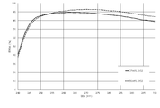
- This is an example of the reflection spectrum of the deep ultraviolet protective film on the glass substrate (Sample No. 2) and the aluminum substrate formed by the resist ink of the present invention in the ultraviolet region to the visible light region.
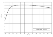
- This is an example of the reflection spectrum in the ultraviolet region of the deep ultraviolet protective film on the glass substrate formed by the resist ink of the present invention (Sample No. 2).
- Condensation type PDMS (polydimethylsilicate) was used as the silicone.
- Dioctyl tin (Nitto Kasei Co., Ltd.) was used as a curing agent for curing silicone.
- zirconium oxide a powder commercially available from Daiichi Rare Element Chemical Industry Co., Ltd. or Nippon Denko Co., Ltd. was used depending on the average particle size. Products with an average particle size (D50) of 0.5 ⁇ m, 1 ⁇ m, 2 ⁇ m, 3 ⁇ m and 14 ⁇ m were used and the deep UV reflectance was compared.
- D50 average particle size
- the resist ink using 0.5 ⁇ m or 1 ⁇ m as the average particle size (D50) of the zirconium oxide powder 60 wt% PDMS, 35 wt% zirconium oxide powder and 5 wt% solvent are centrifuged in a centrifugal stirrer (ARE-made by THINKY). The mixture was mixed by 310), and then precisely dispersed by a three-roll mill (three-roll mill machine manufactured by Inoue Seisakusho). The gap of the three roll mills was set to 15 ⁇ m, and precision dispersion was performed. Texanol was used as the solvent.
- the resist ink using an average particle size (D50) of zirconium oxide powder of 2 ⁇ m, 3 ⁇ m or 14 ⁇ m, 62 wt% PDMS, 36 wt% zirconium oxide powder and 2 wt% solvent (texanol) are mixed by a centrifugal stirrer. After that, it was manufactured by precision dispersion with a three-roll mill. The gap of the three roll mills was set to 15 ⁇ m.
- Resist inks having different contents of zirconium oxide powder were prepared under the following conditions. Using a powder having an average particle size (D50) of zirconium oxide of 0.5 ⁇ m, (60 + X) wt% PDMS, (35-X) wt% zirconium oxide powder and 5 wt% solvent (texanol) are centrifuged and stirred. The mixture was mixed with a vessel and then precisely dispersed with a three-roll mill. The gap of the three roll mills was set to 15 ⁇ m. At this time, X was set to 0, 3 and 5.
- a powder having an average particle size (D50) of zirconium oxide of 0.5 ⁇ m was used, and 58 wt% PDMS, 37 wt% zirconium oxide powder and 5 wt% solvent (texanol) were mixed by a centrifugal stirrer. After that, it was manufactured by precision dispersion with a three-roll mill. Here, the gap of the three roll mill was set to 15 ⁇ m. Further, the sample No. having a zirconium oxide powder content of 50 wt%. In No.
- a powder having an average particle size (D50) of zirconium oxide of 0.5 ⁇ m was used, and 43 wt% PDMS, 50 wt% zirconium oxide powder and 7 wt% solvent (texanol) were mixed by a centrifugal stirrer. After that, it was manufactured by precision dispersion with a three-roll mill. Here, the gap of the three roll mill was set to 15 ⁇ m.
- a resist ink to which zirconium oxide powder and other inorganic powder was added was prepared under the following conditions. Using a powder having an average particle size (D50) of zirconium oxide of 0.5 ⁇ m, centrifuge 35 wt% zirconium oxide powder, (60-Y) wt% PDMS, Y wt% inorganic powder, and 5 wt% solvent (texanol). The mixture was mixed with a separate stirrer and then precisely dispersed with a three-roll mill. The gap of the three roll mills was set to 10 ⁇ m. At this time, Y was set to 30 and 20.
- D50 average particle size of zirconium oxide of 0.5 ⁇ m
- the mixture was mixed with a separate stirrer and then precisely dispersed with
- Titanium oxide Ti-Pure R-101 manufactured by The Chemours
- aluminum oxide AL-S43B manufactured by Sumitomo Chemical Co., Ltd. or AL-45-A manufactured by Showa Denko Co., Ltd.
- a curing agent (Dioctyl tin (Nitto Kasei Co., Ltd.)) was added in an amount of 1 wt% to the resist ink, and the glass substrate was printed by screen printing using a mesh of # 325. The film thickness was adjusted by changing the number of print layers. After printing, the glass substrate was cured at 180 ° C. for 2 hours to prepare a glass substrate with a deep ultraviolet high reflection protective film coated with a resist ink.
- the prepared glass substrate with a deep ultraviolet high reflection protective film was irradiated with ultraviolet rays having a wavelength of 265 nm at 37 mW / cm2 for 1000 hours.
- the change in reflectance at a wavelength of 265 nm before and after irradiation was measured.
- the deep ultraviolet reflectance of the prepared deep ultraviolet reflective substrate and the substrate after ultraviolet irradiation was measured using a spectrophotometer. Diffuse reflectance was measured using an integrating sphere using Spectralon (manufactured by labsphere) as a base.
- Table 1 shows the reflectance of a highly reflective substrate obtained by applying a resist ink prepared using zirconium oxide powder having a different particle size (D50) (content is 32 wt% in each case) and cross-linking and curing. ..
- D50 particle size
- the particle size is 0.5 ⁇ m
- the deep ultraviolet reflectance when the coating film thickness is changed is also shown.
- the reflective substrate obtained by applying a resist ink prepared using zirconium oxide having a particle size of 1 ⁇ m or less and cross-linking and curing the substrate is 250 to 250, except when the film thickness is less than 30 ⁇ m (Sample No. 1). It can be seen that a high reflectance of 85% or more is obtained in the wavelength region of 280 nm.
- Table 2 shows the reflectance of the deep ultraviolet reflective substrate obtained by applying resist inks having different contents of zirconium oxide powder and cross-linking and curing. It can be seen that when the content of the zirconium oxide powder is 32 wt% or more, a high reflectance of 85% or more is obtained in the wavelength region of 250 to 280 nm.
- Table 3 shows the reflectance of the highly reflective substrate obtained by applying and cross-linking and curing a resist ink prepared by mixing zirconium oxide powder and other inorganic powder.
- the deep ultraviolet reflectance of the sample containing the titanium oxide powder is significantly reduced. This is due to the fact that titanium oxide absorbs ultraviolet rays. It can be seen that in the substrate containing the aluminum oxide powder, a high reflectance of 85% or more is obtained in the wavelength region of 250 to 280 nm only when the powder having an average particle size (D50) of 0.8 ⁇ m is used. ..
- the results of evaluating the resistance to deep ultraviolet rays are shown in Table 1.
- the deep ultraviolet resistance is obtained by adjusting ultraviolet rays having a wavelength of 265 nm to 37 mW / cm2, irradiating them for 1000 hours, and measuring the change in reflectance at a wavelength of 265 nm before and after irradiation.
- the sample No. 12
- the amount of change was about 4%.
- Sample No. In 2 and 5 the reflectance at 265 nm after irradiation was 85% or more.
- a glass substrate with a protective film having high diffuse reflectance in the deep ultraviolet region of 250 to 280 nm, which has high diffuse reflectance and excellent resistance to deep ultraviolet, could be applied to produce a glass substrate having high reflection in the deep ultraviolet region.
- FIG. 1 shows a COB substrate on which a deep ultraviolet LED chip 3 is mounted.
- Four deep ultraviolet LED chips 3 are arranged in series by a gold wire 4 and can irradiate a wide range of deep ultraviolet rays.
- the deep ultraviolet rays radiated to the rear are reflected forward without being transmitted and absorbed by the protective film (highly reflective insulating film) 5 formed by using the resist ink of the present invention, and the amount of deep ultraviolet rays increases. ..
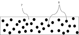
- FIG. 2 is an enlarged view of a protective film (highly reflective insulating film) 5 formed by using the resist ink of the present invention, in which the silicone matrix 7 contains a predetermined content of zirconium oxide powder 8 having a predetermined particle size. It is dispersed in.
- the thickness of the highly reflective insulating film 5 is 30 ⁇ m or more.
- the protective film was translucent (appearingly) in the visible light region.
- FIG. 3 shows the sample No. It shows the reflectance in a wide range from the deep ultraviolet region to the visible light region of No. 2 (solid line). While the reflectance is about 70% to 30% in the visible light region, it selectively shows a high reflectance of 85% or more in the wavelength region of 250 nm to 280 nm, which is the most important deep ultraviolet region for bactericidal action. You can see that.
- An example in which the same protective film is formed on an aluminum substrate with a film thickness of 47 ⁇ m is shown by a broken line in FIG.
- the reflectance from the substrate itself contributes to the reflectance, but the reflectance is 60 to 80% in the visible light region, whereas it is selectively in the wavelength region of 250 nm to 280 nm.
- FIG. 4 shows the sample No. It is an enlarged view of the reflection spectrum in the deep ultraviolet region of No. 2, and it is clear that the reflectance is as high as 85% or more in the wavelength region of 250 nm to 280 nm.
- FIG. 5 shows the sample No.
- the reflection spectra in the deep ultraviolet region of 16 and 17 have a high reflectance of 85% or more in the wavelength region of 250 nm to 280 nm, but when the content of zirconium oxide powder increases, the effect of aggregation appears. Therefore, the reflectance on the long wavelength side increases, but the reflectance on the short wavelength side decreases.
- the content of the zirconium oxide powder is 50 wt%, the reflectance at 250 nm becomes 85%.
- Electrode 1 Electrode 2 ; Sealing resin 3 ; Deep ultraviolet LED chip 4 ; Gold wire 5 ; Protective film (highly reflective insulating film) 6 ... Metal substrate 7 ... Silicone 8 ... Zirconium oxide powder
Landscapes
- Led Device Packages (AREA)
- Inks, Pencil-Leads, Or Crayons (AREA)
- Manufacturing Of Printed Circuit Boards (AREA)
Priority Applications (2)
| Application Number | Priority Date | Filing Date | Title |
|---|---|---|---|
| JP2021573054A JP7343220B2 (ja) | 2020-01-20 | 2021-01-07 | レジストインク |
| CN202180006773.9A CN114762135B (zh) | 2020-01-20 | 2021-01-07 | 光阻墨水 |
Applications Claiming Priority (2)
| Application Number | Priority Date | Filing Date | Title |
|---|---|---|---|
| JP2020007148 | 2020-01-20 | ||
| JP2020-007148 | 2020-01-20 |
Publications (1)
| Publication Number | Publication Date |
|---|---|
| WO2021149497A1 true WO2021149497A1 (ja) | 2021-07-29 |
Family
ID=76992584
Family Applications (1)
| Application Number | Title | Priority Date | Filing Date |
|---|---|---|---|
| PCT/JP2021/000293 Ceased WO2021149497A1 (ja) | 2020-01-20 | 2021-01-07 | レジストインク |
Country Status (4)
| Country | Link |
|---|---|
| JP (1) | JP7343220B2 (cg-RX-API-DMAC7.html) |
| CN (1) | CN114762135B (cg-RX-API-DMAC7.html) |
| TW (1) | TWI821629B (cg-RX-API-DMAC7.html) |
| WO (1) | WO2021149497A1 (cg-RX-API-DMAC7.html) |
Cited By (1)
| Publication number | Priority date | Publication date | Assignee | Title |
|---|---|---|---|---|
| JP7509964B1 (ja) | 2023-02-15 | 2024-07-02 | 光森科技有限公司 | 光源モジュール |
Citations (7)
| Publication number | Priority date | Publication date | Assignee | Title |
|---|---|---|---|---|
| WO2006104061A1 (ja) * | 2005-03-29 | 2006-10-05 | Kyocera Corporation | 反射部材、これを用いた発光装置および照明装置 |
| JP2011258611A (ja) * | 2010-06-04 | 2011-12-22 | Sharp Corp | 発光装置 |
| WO2012144492A1 (ja) * | 2011-04-18 | 2012-10-26 | イビデン株式会社 | Led基板、発光モジュール、led基板の製造方法、及び発光モジュールの製造方法 |
| WO2013154133A1 (ja) * | 2012-04-13 | 2013-10-17 | シャープ株式会社 | 光散乱体、光散乱体膜、光散乱体基板、光散乱体デバイス、発光デバイス、表示装置、および照明装置 |
| JP2014135400A (ja) * | 2013-01-10 | 2014-07-24 | Konica Minolta Inc | 発光装置及び波長変換素子 |
| JP6089144B1 (ja) * | 2016-03-30 | 2017-03-01 | 日本タングステン株式会社 | 銅張積層板およびその製造方法 |
| US20190044033A1 (en) * | 2017-08-03 | 2019-02-07 | Osram Opto Semiconductors Gmbh | Component Having Boundary Element |
Family Cites Families (7)
| Publication number | Priority date | Publication date | Assignee | Title |
|---|---|---|---|---|
| JP2006145915A (ja) * | 2004-11-19 | 2006-06-08 | Mitsubishi Plastics Ind Ltd | 反射フィルム |
| WO2007032217A1 (ja) * | 2005-09-16 | 2007-03-22 | Matsushita Electric Industrial Co., Ltd. | コンポジット材料、及びこれを用いた光学部品 |
| CN102893417B (zh) * | 2010-03-23 | 2016-06-15 | 株式会社朝日橡胶 | 有机硅树脂制反射基材及其制造方法、以及用于该反射基材的原材料组合物 |
| JP2015090395A (ja) * | 2013-11-05 | 2015-05-11 | コニカミノルタ株式会社 | 太陽光反射フィルム、ならびにこれを用いた太陽光反射体および太陽光反射装置 |
| JP2015215413A (ja) * | 2014-05-08 | 2015-12-03 | コニカミノルタ株式会社 | 紫外線遮蔽フィルム |
| JP2020115157A (ja) * | 2017-05-10 | 2020-07-30 | コニカミノルタ株式会社 | 光反射フィルム及び光反射フィルムの製造方法 |
| US11692080B2 (en) * | 2017-08-04 | 2023-07-04 | Sumitomo Osaka Cement Co., Ltd. | Dispersion liquid, composition, sealing member, light-emitting device, illumination tool, display device, and method for producing light-emitting device |
-
2021
- 2021-01-07 CN CN202180006773.9A patent/CN114762135B/zh active Active
- 2021-01-07 JP JP2021573054A patent/JP7343220B2/ja active Active
- 2021-01-07 WO PCT/JP2021/000293 patent/WO2021149497A1/ja not_active Ceased
- 2021-01-14 TW TW110101385A patent/TWI821629B/zh active
Patent Citations (7)
| Publication number | Priority date | Publication date | Assignee | Title |
|---|---|---|---|---|
| WO2006104061A1 (ja) * | 2005-03-29 | 2006-10-05 | Kyocera Corporation | 反射部材、これを用いた発光装置および照明装置 |
| JP2011258611A (ja) * | 2010-06-04 | 2011-12-22 | Sharp Corp | 発光装置 |
| WO2012144492A1 (ja) * | 2011-04-18 | 2012-10-26 | イビデン株式会社 | Led基板、発光モジュール、led基板の製造方法、及び発光モジュールの製造方法 |
| WO2013154133A1 (ja) * | 2012-04-13 | 2013-10-17 | シャープ株式会社 | 光散乱体、光散乱体膜、光散乱体基板、光散乱体デバイス、発光デバイス、表示装置、および照明装置 |
| JP2014135400A (ja) * | 2013-01-10 | 2014-07-24 | Konica Minolta Inc | 発光装置及び波長変換素子 |
| JP6089144B1 (ja) * | 2016-03-30 | 2017-03-01 | 日本タングステン株式会社 | 銅張積層板およびその製造方法 |
| US20190044033A1 (en) * | 2017-08-03 | 2019-02-07 | Osram Opto Semiconductors Gmbh | Component Having Boundary Element |
Cited By (2)
| Publication number | Priority date | Publication date | Assignee | Title |
|---|---|---|---|---|
| JP7509964B1 (ja) | 2023-02-15 | 2024-07-02 | 光森科技有限公司 | 光源モジュール |
| JP2024116055A (ja) * | 2023-02-15 | 2024-08-27 | 光森科技有限公司 | 光源モジュール |
Also Published As
| Publication number | Publication date |
|---|---|
| JPWO2021149497A1 (cg-RX-API-DMAC7.html) | 2021-07-29 |
| CN114762135A (zh) | 2022-07-15 |
| TWI821629B (zh) | 2023-11-11 |
| JP7343220B2 (ja) | 2023-09-12 |
| TW202128894A (zh) | 2021-08-01 |
| CN114762135B (zh) | 2025-04-15 |
Similar Documents
| Publication | Publication Date | Title |
|---|---|---|
| CN104595852B (zh) | 一种波长转换装置、漫反射层、光源系统及投影系统 | |
| KR100713790B1 (ko) | 광원 모듈 및 차량용 전조등 | |
| TWI477555B (zh) | White reflective material and its manufacturing method | |
| EP2160082B1 (en) | Metal base circuit board | |
| EP3144985B1 (en) | Phosphor ceramic, sealed optical semiconductor element, circuit board, optical semiconductor device and light-emitting device | |
| TWI535792B (zh) | Led封裝材料 | |
| US20230167357A1 (en) | Phosphor wheel with inorganic binder | |
| CN102725872A (zh) | Led包封树脂体,led装置和led装置的制造方法 | |
| EP2506320A1 (en) | Substrate for led mounting | |
| CN105045022B (zh) | 光源系统及其波长转换装置 | |
| EP3451031B1 (en) | Wavelength conversion member, production method therefor, and light emitting device | |
| JP2012064928A (ja) | 半導体発光装置用樹脂成形体用材料及び樹脂成形体 | |
| JP2021155256A (ja) | 分散液、組成物、封止部材、発光装置、照明器具、表示装置および分散液の製造方法 | |
| JP2016108216A (ja) | 蛍光体分散ガラス | |
| JP7343220B2 (ja) | レジストインク | |
| JPWO2008078711A1 (ja) | 蛍光体およびその製法ならびに波長変換器、発光装置、照明装置 | |
| KR20110013907A (ko) | 높은 열전도 효율을 가지는 방열 패드 및 이의 제조방법 | |
| EP3136454A1 (en) | Wavelength conversion joining member, wavelength conversion heat-radiating member, and light emission device | |
| CN102959745B (zh) | Led装置及其制造方法 | |
| CN111029452B (zh) | 一种紫外发光二极管封装结构及其封装方法、和紫外灯 | |
| JP2021155261A (ja) | 分散液、組成物、封止部材、発光装置、照明器具、表示装置 | |
| EP2372799A2 (en) | Highly reflective white material and led package | |
| JP5635189B2 (ja) | 蛍光体の改良 | |
| JP2020107794A (ja) | Led搭載用基板及び照明装置 | |
| US9203002B2 (en) | Ultraviolet reflective silicone compositions, reflectors, and light sources incorporating the same |
Legal Events
| Date | Code | Title | Description |
|---|---|---|---|
| 121 | Ep: the epo has been informed by wipo that ep was designated in this application |
Ref document number: 21744334 Country of ref document: EP Kind code of ref document: A1 |
|
| ENP | Entry into the national phase |
Ref document number: 2021573054 Country of ref document: JP Kind code of ref document: A |
|
| NENP | Non-entry into the national phase |
Ref country code: DE |
|
| 122 | Ep: pct application non-entry in european phase |
Ref document number: 21744334 Country of ref document: EP Kind code of ref document: A1 |
|
| WWG | Wipo information: grant in national office |
Ref document number: 202180006773.9 Country of ref document: CN |