WO2021145428A1 - センサ用出力装置 - Google Patents
センサ用出力装置 Download PDFInfo
- Publication number
- WO2021145428A1 WO2021145428A1 PCT/JP2021/001246 JP2021001246W WO2021145428A1 WO 2021145428 A1 WO2021145428 A1 WO 2021145428A1 JP 2021001246 W JP2021001246 W JP 2021001246W WO 2021145428 A1 WO2021145428 A1 WO 2021145428A1
- Authority
- WO
- WIPO (PCT)
- Prior art keywords
- impedance
- output
- sensor
- unit
- output device
- Prior art date
- Legal status (The legal status is an assumption and is not a legal conclusion. Google has not performed a legal analysis and makes no representation as to the accuracy of the status listed.)
- Ceased
Links
Images



Classifications
-
- G—PHYSICS
- G01—MEASURING; TESTING
- G01D—MEASURING NOT SPECIALLY ADAPTED FOR A SPECIFIC VARIABLE; ARRANGEMENTS FOR MEASURING TWO OR MORE VARIABLES NOT COVERED IN A SINGLE OTHER SUBCLASS; TARIFF METERING APPARATUS; MEASURING OR TESTING NOT OTHERWISE PROVIDED FOR
- G01D5/00—Mechanical means for transferring the output of a sensing member; Means for converting the output of a sensing member to another variable where the form or nature of the sensing member does not constrain the means for converting; Transducers not specially adapted for a specific variable
- G01D5/12—Mechanical means for transferring the output of a sensing member; Means for converting the output of a sensing member to another variable where the form or nature of the sensing member does not constrain the means for converting; Transducers not specially adapted for a specific variable using electric or magnetic means
Definitions
- the present invention relates to an improvement of an output device for a sensor.
- a sensor output device is attached to the sensor to amplify or convert the change in the amount of electricity in the sensor so that it can be detected by a general-purpose detection device.
- a Wheatstone bridge circuit is known as an output device for a sensor that is attached to a sensor that converts a change in pressure into a change in electrical resistance (such as pressure-sensitive conductive rubber) and amplifies the change in electrical resistance.
- Patent Document 1 discloses a device that uses an oscillation circuit as an output device that responds to changes in electrical resistance (hereinafter, may be simply referred to as "resistance").
- the resistance portion is used as a sensor, and the change in the resistance is output as the change in frequency.
- the accuracy of a capacitor refers to the ratio of capacitance that changes in response to changes in the external environment such as temperature.
- the one with high accuracy means that the change (sensitivity) of the capacity in response to the change of the external environment is small. This may be explained in this specification as having a low sensitivity to changes in the external environment. It is unclear how much measurement accuracy is obtained with this sensor output device. In particular, when the accuracy of the capacitor becomes as high as the resistance, for example, when the accuracy of both becomes 10-5 to 10-6 / ° C, how much is the measurement accuracy of the output device for the sensor? It was unclear if it would be.
- the measurement accuracy becomes equal to the accuracy of the capacitor itself (external environment change sensitivity) (external). I noticed that the sensitivity to environmental changes decreases). Equal here includes errors to the extent that those skilled in the art can understand.
- the measurement accuracy of the oscillator circuit type sensor output device pointed to ⁇ 1500 ⁇ 10-6 / ° C. At this time, the accuracy of the capacitor was ⁇ 60.0 ⁇ 10-6 / ° C, and the accuracy (rating) of the resistor was ⁇ 5 ⁇ 10-6 / ° C.
- the vertical axis (left side) represents the rate of change in frequency
- the horizontal axis represents the passage of time.
- the oscillator circuit type sensor output device also has high accuracy by selecting the resistor and the capacitor having high accuracy. In other words, high-precision output has become possible with a simple circuit configuration. Since such an oscillation circuit consumes less power, the application of the sensor output device is expanded.
- FIG. 1 As shown by the vertical axis in FIG. 1, the magnitude of the diurnal change in the output of the oscillator circuit type sensor output device that the authors experimented with was ⁇ 1500 ⁇ 10-6 with respect to a change of about 8 ° C. ( In the figure, it is converted into the rate of change in frequency, and the unit is 10-6 ).
- the accuracy of the capacitor in the circuit at the time of this experiment was ⁇ 60 ⁇ 10-6 / ° C, and the accuracy (rated) of the resistor was ⁇ 5 ⁇ 10-6 / ° C.
- the horizontal axis indicates the passage of time.
- the data in FIG. 1 is not the result of directly measuring the frequency, but the result obtained by counting the frequency division period obtained by dividing the frequency with a clock of 10 MHz, and in order to achieve such measurement accuracy.
- the change of the waveform output by the sensor output device is analyzed with a clock of 1 MHz or more.
- FIG. 1 since the ratio of the output change of the oscillator circuit type sensor output device has a large diurnal change, it can be seen that the output frequency changes under the influence of temperature. Another object of the present invention is to further improve the accuracy of such an oscillator circuit type sensor output device.
- the present inventors arranged a reference resistor RA in the vicinity of the resistor RB serving as a sensor, and constructed an oscillation circuit (second oscillation circuit section) using the reference resistor RA.
- the second oscillation circuit section is the same as the first oscillation circuit section except for the resistor RB portion (see FIGS. 2 and 4).
- An oscillation circuit (second oscillation circuit section) provided with a reference resistor RA may be referred to as a reference waveform output section.
- an oscillation circuit (first oscillation circuit unit) provided with a resistor RB that serves as a sensor may be referred to as a measurement waveform output unit.
- This reference waveform output unit may be independent of the measurement waveform output unit including the resistance RB serving as a sensor (see FIG. 4), or may be shared by other than the resistance portion (see FIG. 2). The latter (FIG. 2) is preferable from the viewpoint of bringing the resistor RB and the reference resistor RA close to each other and reducing the number of parts.
- the output from the measurement waveform output unit and the output from the reference waveform output unit are switched every 0.45 seconds, and the former is corrected by the latter. That is, the output of the latter was subtracted from the output of the former. And this is repeated.
- the magnitude of the corrected diurnal change on the chart was ⁇ 10 ⁇ 10-6 or less with respect to the change of about 8 ° C. That is, the amplitude ⁇ 1500 ⁇ 10 -6 is a previous value of the difference processing becomes smaller amplitude ⁇ 10 ⁇ 10 -6 2 digits or more, so that the measurement accuracy is improved.
- the aim is to improve the accuracy of correction by preventing a time difference between the output from the measurement waveform output unit and the output from the reference waveform output unit.
- the time difference is at least 10 seconds or less, more preferably 1 second or less. It is more effective if the time difference is small in order to eliminate the drift generated in the electronic circuit.
- the output from the measurement waveform output unit and the reference waveform output unit is preferably a rectangular wave. This is because it is easy to specify the frequency by using the rising portion and / or the falling portion of the rectangular wave.
- the waveform analysis unit 10 counts the number of clocks included in one square wave. As a result, the time of 1/2 wavelength is specified, and the frequency is calculated.
- the output waveform from the reference waveform output unit is also processed in the same manner. Since the output waveform from the measurement waveform output unit and the output waveform from the reference waveform output unit are distinguished, the amplitude of both and the ratio of the rectangular wave to one wavelength can be changed.
- a waveform having a wavelength of 1/2 or more can be used, or a frequency dividing circuit can be provided to lower the output frequency.
- the output of the waveform analysis unit 10 is digital data having a frequency. Therefore, such output amplification is easily performed, and noise superimposed during transmission can be easily removed.
- the output from the waveform analysis unit 10 is simply digital data representing the frequency, so any output. It cannot be determined whether it is due to a wave. Therefore, a signal for determining the first timing (for example, time t1) for inputting the output waveform from the measurement waveform output unit to the waveform analysis unit 10 is input from the timing generation unit 21 of the frequency correction unit (output correction unit) 20.
- the frequency subtraction unit 25 stores the first timing (time t1).
- a signal for determining a second timing for example, time t2 for inputting the output waveform from the reference waveform output unit to the waveform analysis unit 10 is input from the timing generation unit 21.
- the frequency subtraction unit 25 stores the second timing (time t2).
- the position of the output waveform from the measurement waveform output unit (time series arrangement) and the position of the output waveform from the reference waveform output unit (time series arrangement) are determined on a common time axis.
- the input signal from the timing generator and the output signal of the measurement waveform are preferably in the form of passing through an isolated device such as a photocoupler, and in such a form, the oscillation circuit is less likely to be affected by external noise.
- the frequency correction unit 20 corrects the frequency based on the output waveform of the measurement waveform output unit obtained at the first timing with reference to the frequency based on the output waveform from the reference waveform output unit obtained from the second timing. do.
- the frequency subtraction unit 25 subtracts the frequency based on the output waveform from the reference waveform output unit from the frequency based on the output waveform from the measurement waveform output unit.
- the frequency obtained at the first timing is corrected by the frequency obtained at the second timing immediately after.
- the frequency obtained at the first timing may be corrected by the frequency obtained at the second timing immediately before.
- FIG. 1 is a chart showing an output waveform of the sensor output device of the present invention.
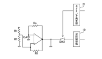
- FIG. 2 is a circuit diagram showing a configuration of a sensor output device according to an embodiment of the present invention.
- FIG. 3 is a circuit diagram showing a configuration of a sensor output device according to another embodiment of the present invention.
- FIG. 4 is a circuit diagram showing a configuration of a sensor output device according to another embodiment of the present invention.
- FIG. 5 is a circuit diagram showing a configuration of a sensor output device according to another embodiment of the present invention.
- FIG. 6 is a circuit diagram showing a configuration of a sensor output device according to another embodiment of the present invention.
- FIG. 7 is a chart showing the output of the sensor output device of FIG.
- FIG. 8 is a chart showing the difference in output of the output device for the sensor of FIG.
- the configuration of the sensor output device 1 according to the embodiment of the present invention is shown in FIG.
- the sensor output device 1 is composed of an oscillation circuit unit 5, a waveform adjustment unit 7, a waveform analysis unit 10, a frequency correction unit 20, and a specific unit 30.
- the oscillation circuit unit 5 is a general-purpose oscillation circuit composed of a resistor RB as a first impedance unit, a capacitor CA as a second impedance unit, and a comparator.
- the resistance RB for measurement corresponds to a part of the sensor made of pressure-sensitive conductive rubber, and the resistance changes according to the pressure applied to the sensor.
- the reference resistor RA is arranged in the vicinity of the resistor RB.
- the accuracy of this reference resistor RA against temperature changes is ⁇ 5 ⁇ 10 -6 / ° C, which is higher than that of the resistor RB made of pressure-sensitive conductive rubber. That of the capacitor CA was ⁇ 60 ⁇ 10-6 / ° C.
- the measurement resistor RB and the reference resistor RA are switched by the switch SW1 as a switching unit.
- the state of the oscillation circuit unit 5 in which the resistor RB is selected is the measurement mode
- the state of the oscillation circuit unit 5 in which the reference resistor RA is selected is the reference mode.
- an RC circuit was adopted as the oscillation circuit, but if you are a skilled person, you can select at least two impedance elements consisting of a resistor, a capacitor, and a coil, or a configuration that combines an inverter or NAND gate as shown in FIG. It can be easily assumed that an oscillator circuit can be constructed.
- the waveform adjusting unit 7 changes the waveform (rectangular wave) between the output of the measurement mode and the output of the reference mode.
- the amplitude of the output waveform is changed by switching the switch SW2 in synchronization with the switch SW1.
- the waveform analysis unit 10 specifies the frequency of the square wave. That is, the number of clocks from the rising edge of the rectangular wave to the falling edge is counted. It is assumed that 1 MHz or more is used as the clock. Since the time of a square wave (that is, 1/2 wavelength) is specified from the number of clocks, the frequency can be calculated. Of course, the number of clocks included in a plurality of consecutive rectangular waves may be counted.
- the frequency is stored in the frequency storage unit 23 of the frequency correction unit 20 as the output correction unit. Since the output of the waveform analysis unit 10 is merely frequency-related data, it is not possible to specify from the data alone whether it is derived from the measurement mode or the reference mode. Therefore, in this example, the switching timing (time t1) of the switch SW1 is controlled by a signal from the timing generation unit 21. The timing (time t1) at which the switching signal is output from the timing generation unit 21 is sent to the frequency storage unit 23, and is stored in association with the data sent from the waveform analysis unit 10. As a result, the data related to the frequency stored in the frequency storage unit 23 is associated with the time obtained.
- the frequency subtraction unit 25 subtracts the frequency (time t2) in the reference mode immediately after switching the switch SW1 from the frequency (time t1) in the measurement mode. Then, the frequency (time t4) in the reference mode immediately after the switch SW1 is switched again is subtracted from the frequency (time t3) in the measurement mode immediately after the switch SW1 is switched. After that, this is repeated.
- the identification unit 30 identifies the pressure change by comparing the frequency change corrected by the frequency correction unit 20 with the calibration data obtained in advance.
- the identified pressure change that is, the change in the characteristics of the sensor object, is presented to the observer through a monitor (not shown).
- the circuit of FIG. 2 has a small number of parts and can be miniaturized. If the strain gauge used in many applications is used as a resistor RB and integrated with the miniaturized circuit according to the present invention, the lead wire of the strain gauge can be shortened and highly accurate strain measurement becomes possible. Become. The difficulty in the measurement using the strain gauge is that the measurement result is disturbed by the change in the resistance value generated in the lead wire due to the change in the environmental temperature and the influence of the external noise superimposed on the lead wire.
- the length of the lead wire can be reduced to about several cm or less, the above-mentioned difficulty can be solved and high-precision measurement can be performed. If the measurement target is a conductor, if the entire circuit integrated with the strain gauge is covered with a conductor, including the lead wire, the influence of external noise will be completely eliminated and the strain will be measured with higher accuracy. Can be done.
- the resistance side is responsible for the sensor function, but the capacitor may be responsible for the sensor function (see FIG. 3).
- elements having the same functions as those in FIG. 2 are designated by the same reference numerals, and the description thereof will be partially omitted.
- the reference capacitor CA and the measurement capacitor CB are switched by the switch SW101 in the oscillation circuit unit 105.
- the oscillation circuit unit 205 for the measurement mode (first oscillation circuit, measurement waveform output unit) and the oscillation circuit unit 305 for the reference mode (second oscillation circuit, reference waveform output unit) are separate. It is a body, and a waveform analysis unit 10 is attached to each body.
- the output timing of the oscillation circuit units 205 and 305 is controlled by the timing signal input from the timing generation unit 21 to the switches SW201 and SW301. The time is specified and used for frequency correction in the frequency correction unit.
- SW1 selects two states, a measurement mode and a reference mode, but it is preferable to further include a pause mode.
- this hibernation mode no power is supplied to either the reference resistor RA or the resistor RB. By providing such a hibernation mode, power consumption can be reduced.
- FIG. 5 shows the configuration of the sensor output device of another embodiment.
- an oscillator circuit is composed of an inverter for a digital circuit (for example, TC74HC04 manufactured by Toshiba) and a NAND gate (for example, TC74HC00 manufactured by Toshiba), and a three-state buffer is set in the switch SW3 for switching between the measurement mode and the reference mode.
- TC74HC126 or TC74HC125 manufactured by Toshiba can be used.
- a reference mode for activating the reference resistor RA and a measurement mode for activating the resistor RB can be selected based on the signal from the timing generation unit 21. Further, if the L level signal from the timing generation circuit is input to the NAND gate, the output of the gate becomes the L level, the oscillation is stopped, the hibernation mode is set, and the current consumption at DC5V becomes 20 ⁇ A or less.
- the resistance value of the reference resistance RA is also 120 ⁇ , and when the power supply is DC5V, the reference resistance RA and the resistance RB have a maximum of 41.7mA. Current flows. Therefore, the hibernation mode is selected so that the circuit is not oscillated during unnecessary time and unnecessary current is not passed through the reference resistor RA and the resistor RB.
- the measurement accuracy is improved by adopting the three-state buffer as the switch SW3.
- the ON resistance does not always become a constant value, but if the three-state buffer is adopted as the switch SW3, the ON resistance becomes constant, so that the measurement accuracy is considered to be improved. ..
- FIG. 6 shows the configuration of the sensor output device of another embodiment.
- the reference resistor RA that uses a comparator that suppresses zero drift and executes the reference mode is omitted.
- the change in resistance value obtained from the frequency change of such a device was about ⁇ 80 ppm with respect to the temperature change of ⁇ 5 ° C. (see FIG. 7).
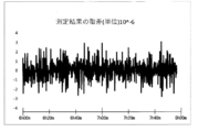
- FIG. 8 shows the difference in resistance value change. It can be seen that the standard deviation of the 50 data at the beginning of FIG. 8 is a little less than 1.0 ⁇ 10-6 , and the rate of change in resistance in a short time is about ⁇ 1.0 ⁇ 10-6.
- the amplitude of the diurnal change in frequency is about 160 ppm, and a highly accurate measurement result can be obtained. This is due to the use of a comparator that suppresses zero drift.
- a comparator (TS3011) manufactured by Kus Co., Ltd. was used for STMicroelectronics.
- An oscillation circuit can be configured even when a Schmitt trigger input inverter for digital circuits (for example, TC74HC14 manufactured by Toshiba) is used, but the inverter has a more uncertain signal high / low switching threshold than the comparator, so subtle temperature changes occur.
- the threshold value of the inverter itself may be affected and the measurement result may be disturbed.
- the comparator that suppresses zero drift it is considered that the threshold value is stable and the measurement result is not easily disturbed.
- an operational amplifier or a zero drift amplifier can be used instead of the comparator.
- more power saving can be achieved by using a low power consumption comparator, an operational amplifier, and a zero drift amplifier, and if a sleep mode is provided, it can be oscillated only when necessary. Further power saving can be achieved.
- the circuit of FIG. 6 since the parts necessary for selecting the reference resistor are omitted, the circuit can be miniaturized, and it is less affected by external noise, and there is an advantage that the space at the time of assembling or the like can be omitted.
Landscapes
- Physics & Mathematics (AREA)
- General Physics & Mathematics (AREA)
- Measuring Fluid Pressure (AREA)
Priority Applications (1)
| Application Number | Priority Date | Filing Date | Title |
|---|---|---|---|
| JP2021571261A JP7818220B2 (ja) | 2020-01-15 | 2021-01-15 | センサ用出力装置 |
Applications Claiming Priority (2)
| Application Number | Priority Date | Filing Date | Title |
|---|---|---|---|
| JP2020-004789 | 2020-01-15 | ||
| JP2020004789 | 2020-01-15 |
Publications (1)
| Publication Number | Publication Date |
|---|---|
| WO2021145428A1 true WO2021145428A1 (ja) | 2021-07-22 |
Family
ID=76863779
Family Applications (1)
| Application Number | Title | Priority Date | Filing Date |
|---|---|---|---|
| PCT/JP2021/001246 Ceased WO2021145428A1 (ja) | 2020-01-15 | 2021-01-15 | センサ用出力装置 |
Country Status (2)
| Country | Link |
|---|---|
| JP (1) | JP7818220B2 (https=) |
| WO (1) | WO2021145428A1 (https=) |
Cited By (1)
| Publication number | Priority date | Publication date | Assignee | Title |
|---|---|---|---|---|
| JP2023131768A (ja) * | 2022-03-09 | 2023-09-22 | 常生 山内 | 変位測定装置 |
Citations (5)
| Publication number | Priority date | Publication date | Assignee | Title |
|---|---|---|---|---|
| JP2005300519A (ja) * | 2004-03-19 | 2005-10-27 | Nippon Soken Inc | センサ装置 |
| JP2008164380A (ja) * | 2006-12-27 | 2008-07-17 | Denso Corp | 湿度センサ装置 |
| JP2008197060A (ja) * | 2007-02-15 | 2008-08-28 | Tokai Rubber Ind Ltd | 変形センサシステム |
| JP2013024808A (ja) * | 2011-07-25 | 2013-02-04 | Japan Aerospace Exploration Agency | 計測装置および計測方法 |
| CN104135244A (zh) * | 2014-07-24 | 2014-11-05 | 深圳市锐能微科技有限公司 | 一种电阻工艺偏差的补偿方法、装置、电阻及rc振荡器 |
Family Cites Families (4)
| Publication number | Priority date | Publication date | Assignee | Title |
|---|---|---|---|---|
| JPS56145315A (en) * | 1980-04-15 | 1981-11-12 | Yokogawa Hokushin Electric Corp | Displacement converting method |
| JP3198748B2 (ja) * | 1993-02-27 | 2001-08-13 | オムロン株式会社 | 静電容量検出回路 |
| JP3428319B2 (ja) * | 1996-09-30 | 2003-07-22 | オムロン株式会社 | 静電容量検出回路および静電容量型センサ装置 |
| WO2001096815A1 (fr) * | 2000-06-14 | 2001-12-20 | Omron Corporation | Dispositif de transformation de la sortie d'un capteur |
-
2021
- 2021-01-15 JP JP2021571261A patent/JP7818220B2/ja active Active
- 2021-01-15 WO PCT/JP2021/001246 patent/WO2021145428A1/ja not_active Ceased
Patent Citations (5)
| Publication number | Priority date | Publication date | Assignee | Title |
|---|---|---|---|---|
| JP2005300519A (ja) * | 2004-03-19 | 2005-10-27 | Nippon Soken Inc | センサ装置 |
| JP2008164380A (ja) * | 2006-12-27 | 2008-07-17 | Denso Corp | 湿度センサ装置 |
| JP2008197060A (ja) * | 2007-02-15 | 2008-08-28 | Tokai Rubber Ind Ltd | 変形センサシステム |
| JP2013024808A (ja) * | 2011-07-25 | 2013-02-04 | Japan Aerospace Exploration Agency | 計測装置および計測方法 |
| CN104135244A (zh) * | 2014-07-24 | 2014-11-05 | 深圳市锐能微科技有限公司 | 一种电阻工艺偏差的补偿方法、装置、电阻及rc振荡器 |
Cited By (1)
| Publication number | Priority date | Publication date | Assignee | Title |
|---|---|---|---|---|
| JP2023131768A (ja) * | 2022-03-09 | 2023-09-22 | 常生 山内 | 変位測定装置 |
Also Published As
| Publication number | Publication date |
|---|---|
| JP7818220B2 (ja) | 2026-02-20 |
| JPWO2021145428A1 (https=) | 2021-07-22 |
Similar Documents
| Publication | Publication Date | Title |
|---|---|---|
| JP6916441B2 (ja) | 半導体集積回路及び呼吸運動検査装置 | |
| KR20220027815A (ko) | 온도 측정 회로, 온도 및 광 측정 회로, 온도 측정 방법 및 온도 및 광 측정 방법 | |
| US9784632B2 (en) | Sensor signal detection device | |
| KR102234612B1 (ko) | 근접 센서에서의 환경 보상 방법 및 개선된 환경 보상 성능을 가진 근접 센서 | |
| US20120062500A1 (en) | Adaptive high dynamic range surface capacitive touchscreen controller | |
| US12270870B2 (en) | Magnetic sensor and biomagnetic measurement device | |
| US20230297188A1 (en) | Multichannel capacitive sensor device | |
| US20150234017A1 (en) | Magnetic field detecting device | |
| US6753686B2 (en) | Method and apparatus for detecting failure of differential transformer, and method and apparatus for signal processing of differential transformer | |
| WO2021145428A1 (ja) | センサ用出力装置 | |
| US10320039B2 (en) | Semiconductor device, battery monitoring system, and method of monitoring battery | |
| JP6718284B2 (ja) | 信号処理回路、クーロンカウンタ回路、電子機器 | |
| KR101220936B1 (ko) | 기생정전용량을 가지는 정전용량형 센서의 정전용량 측정회로 | |
| US11536616B2 (en) | Sensor device and method for operating a sensor device | |
| US20210333233A1 (en) | Semiconductor device, biological signal sensor and biological signal sensor system | |
| CN115950570B (zh) | 压力测量电路、芯片及电子设备 | |
| JP4161873B2 (ja) | 静電容量型距離センサ | |
| KR20190064987A (ko) | 비접촉 심전도 측정 방법, 비접촉 심전도 측정 회로 및 이를 이용한 심전도 측정 장치 | |
| CN113155159A (zh) | 桥式检测器 | |
| EP3130894B1 (en) | Abnormality detection device for sensor and sensor device | |
| JPWO2021145428A5 (https=) | ||
| KR101665187B1 (ko) | 환경 정보 센서 회로 및 환경 정보 측정 장치 | |
| KR101879201B1 (ko) | 전자기 유도 입력 방식의 센싱 장치 및 그 제어 방법 | |
| US12478264B2 (en) | System for sensing arterial pulse waveform | |
| EP3187847B1 (en) | Pressure measurement |
Legal Events
| Date | Code | Title | Description |
|---|---|---|---|
| 121 | Ep: the epo has been informed by wipo that ep was designated in this application |
Ref document number: 21741859 Country of ref document: EP Kind code of ref document: A1 |
|
| ENP | Entry into the national phase |
Ref document number: 2021571261 Country of ref document: JP Kind code of ref document: A |
|
| NENP | Non-entry into the national phase |
Ref country code: DE |
|
| 122 | Ep: pct application non-entry in european phase |
Ref document number: 21741859 Country of ref document: EP Kind code of ref document: A1 |