WO2021145428A1 - Output device for sensor - Google Patents
Output device for sensor Download PDFInfo
- Publication number
- WO2021145428A1 WO2021145428A1 PCT/JP2021/001246 JP2021001246W WO2021145428A1 WO 2021145428 A1 WO2021145428 A1 WO 2021145428A1 JP 2021001246 W JP2021001246 W JP 2021001246W WO 2021145428 A1 WO2021145428 A1 WO 2021145428A1
- Authority
- WO
- WIPO (PCT)
- Prior art keywords
- impedance
- output
- sensor
- unit
- output device
- Prior art date
Links
Images


Classifications
-
- G—PHYSICS
- G01—MEASURING; TESTING
- G01D—MEASURING NOT SPECIALLY ADAPTED FOR A SPECIFIC VARIABLE; ARRANGEMENTS FOR MEASURING TWO OR MORE VARIABLES NOT COVERED IN A SINGLE OTHER SUBCLASS; TARIFF METERING APPARATUS; MEASURING OR TESTING NOT OTHERWISE PROVIDED FOR
- G01D5/00—Mechanical means for transferring the output of a sensing member; Means for converting the output of a sensing member to another variable where the form or nature of the sensing member does not constrain the means for converting; Transducers not specially adapted for a specific variable
- G01D5/12—Mechanical means for transferring the output of a sensing member; Means for converting the output of a sensing member to another variable where the form or nature of the sensing member does not constrain the means for converting; Transducers not specially adapted for a specific variable using electric or magnetic means
Definitions
- the present invention relates to an improvement of an output device for a sensor.
- a sensor output device is attached to the sensor to amplify or convert the change in the amount of electricity in the sensor so that it can be detected by a general-purpose detection device.
- a Wheatstone bridge circuit is known as an output device for a sensor that is attached to a sensor that converts a change in pressure into a change in electrical resistance (such as pressure-sensitive conductive rubber) and amplifies the change in electrical resistance.
- Patent Document 1 discloses a device that uses an oscillation circuit as an output device that responds to changes in electrical resistance (hereinafter, may be simply referred to as "resistance").
- the resistance portion is used as a sensor, and the change in the resistance is output as the change in frequency.
- the accuracy of a capacitor refers to the ratio of capacitance that changes in response to changes in the external environment such as temperature.
- the one with high accuracy means that the change (sensitivity) of the capacity in response to the change of the external environment is small. This may be explained in this specification as having a low sensitivity to changes in the external environment. It is unclear how much measurement accuracy is obtained with this sensor output device. In particular, when the accuracy of the capacitor becomes as high as the resistance, for example, when the accuracy of both becomes 10-5 to 10-6 / ° C, how much is the measurement accuracy of the output device for the sensor? It was unclear if it would be.
- the measurement accuracy becomes equal to the accuracy of the capacitor itself (external environment change sensitivity) (external). I noticed that the sensitivity to environmental changes decreases). Equal here includes errors to the extent that those skilled in the art can understand.
- the measurement accuracy of the oscillator circuit type sensor output device pointed to ⁇ 1500 ⁇ 10-6 / ° C. At this time, the accuracy of the capacitor was ⁇ 60.0 ⁇ 10-6 / ° C, and the accuracy (rating) of the resistor was ⁇ 5 ⁇ 10-6 / ° C.
- the vertical axis (left side) represents the rate of change in frequency
- the horizontal axis represents the passage of time.
- the oscillator circuit type sensor output device also has high accuracy by selecting the resistor and the capacitor having high accuracy. In other words, high-precision output has become possible with a simple circuit configuration. Since such an oscillation circuit consumes less power, the application of the sensor output device is expanded.
- FIG. 1 As shown by the vertical axis in FIG. 1, the magnitude of the diurnal change in the output of the oscillator circuit type sensor output device that the authors experimented with was ⁇ 1500 ⁇ 10-6 with respect to a change of about 8 ° C. ( In the figure, it is converted into the rate of change in frequency, and the unit is 10-6 ).
- the accuracy of the capacitor in the circuit at the time of this experiment was ⁇ 60 ⁇ 10-6 / ° C, and the accuracy (rated) of the resistor was ⁇ 5 ⁇ 10-6 / ° C.
- the horizontal axis indicates the passage of time.
- the data in FIG. 1 is not the result of directly measuring the frequency, but the result obtained by counting the frequency division period obtained by dividing the frequency with a clock of 10 MHz, and in order to achieve such measurement accuracy.
- the change of the waveform output by the sensor output device is analyzed with a clock of 1 MHz or more.
- FIG. 1 since the ratio of the output change of the oscillator circuit type sensor output device has a large diurnal change, it can be seen that the output frequency changes under the influence of temperature. Another object of the present invention is to further improve the accuracy of such an oscillator circuit type sensor output device.
- the present inventors arranged a reference resistor RA in the vicinity of the resistor RB serving as a sensor, and constructed an oscillation circuit (second oscillation circuit section) using the reference resistor RA.
- the second oscillation circuit section is the same as the first oscillation circuit section except for the resistor RB portion (see FIGS. 2 and 4).
- An oscillation circuit (second oscillation circuit section) provided with a reference resistor RA may be referred to as a reference waveform output section.
- an oscillation circuit (first oscillation circuit unit) provided with a resistor RB that serves as a sensor may be referred to as a measurement waveform output unit.
- This reference waveform output unit may be independent of the measurement waveform output unit including the resistance RB serving as a sensor (see FIG. 4), or may be shared by other than the resistance portion (see FIG. 2). The latter (FIG. 2) is preferable from the viewpoint of bringing the resistor RB and the reference resistor RA close to each other and reducing the number of parts.
- the output from the measurement waveform output unit and the output from the reference waveform output unit are switched every 0.45 seconds, and the former is corrected by the latter. That is, the output of the latter was subtracted from the output of the former. And this is repeated.
- the magnitude of the corrected diurnal change on the chart was ⁇ 10 ⁇ 10-6 or less with respect to the change of about 8 ° C. That is, the amplitude ⁇ 1500 ⁇ 10 -6 is a previous value of the difference processing becomes smaller amplitude ⁇ 10 ⁇ 10 -6 2 digits or more, so that the measurement accuracy is improved.
- the aim is to improve the accuracy of correction by preventing a time difference between the output from the measurement waveform output unit and the output from the reference waveform output unit.
- the time difference is at least 10 seconds or less, more preferably 1 second or less. It is more effective if the time difference is small in order to eliminate the drift generated in the electronic circuit.
- the output from the measurement waveform output unit and the reference waveform output unit is preferably a rectangular wave. This is because it is easy to specify the frequency by using the rising portion and / or the falling portion of the rectangular wave.
- the waveform analysis unit 10 counts the number of clocks included in one square wave. As a result, the time of 1/2 wavelength is specified, and the frequency is calculated.
- the output waveform from the reference waveform output unit is also processed in the same manner. Since the output waveform from the measurement waveform output unit and the output waveform from the reference waveform output unit are distinguished, the amplitude of both and the ratio of the rectangular wave to one wavelength can be changed.
- a waveform having a wavelength of 1/2 or more can be used, or a frequency dividing circuit can be provided to lower the output frequency.
- the output of the waveform analysis unit 10 is digital data having a frequency. Therefore, such output amplification is easily performed, and noise superimposed during transmission can be easily removed.
- the output from the waveform analysis unit 10 is simply digital data representing the frequency, so any output. It cannot be determined whether it is due to a wave. Therefore, a signal for determining the first timing (for example, time t1) for inputting the output waveform from the measurement waveform output unit to the waveform analysis unit 10 is input from the timing generation unit 21 of the frequency correction unit (output correction unit) 20.
- the frequency subtraction unit 25 stores the first timing (time t1).
- a signal for determining a second timing for example, time t2 for inputting the output waveform from the reference waveform output unit to the waveform analysis unit 10 is input from the timing generation unit 21.
- the frequency subtraction unit 25 stores the second timing (time t2).
- the position of the output waveform from the measurement waveform output unit (time series arrangement) and the position of the output waveform from the reference waveform output unit (time series arrangement) are determined on a common time axis.
- the input signal from the timing generator and the output signal of the measurement waveform are preferably in the form of passing through an isolated device such as a photocoupler, and in such a form, the oscillation circuit is less likely to be affected by external noise.
- the frequency correction unit 20 corrects the frequency based on the output waveform of the measurement waveform output unit obtained at the first timing with reference to the frequency based on the output waveform from the reference waveform output unit obtained from the second timing. do.
- the frequency subtraction unit 25 subtracts the frequency based on the output waveform from the reference waveform output unit from the frequency based on the output waveform from the measurement waveform output unit.
- the frequency obtained at the first timing is corrected by the frequency obtained at the second timing immediately after.
- the frequency obtained at the first timing may be corrected by the frequency obtained at the second timing immediately before.
- FIG. 1 is a chart showing an output waveform of the sensor output device of the present invention.
- FIG. 2 is a circuit diagram showing a configuration of a sensor output device according to an embodiment of the present invention.
- FIG. 3 is a circuit diagram showing a configuration of a sensor output device according to another embodiment of the present invention.
- FIG. 4 is a circuit diagram showing a configuration of a sensor output device according to another embodiment of the present invention.
- FIG. 5 is a circuit diagram showing a configuration of a sensor output device according to another embodiment of the present invention.
- FIG. 6 is a circuit diagram showing a configuration of a sensor output device according to another embodiment of the present invention.
- FIG. 7 is a chart showing the output of the sensor output device of FIG.
- FIG. 8 is a chart showing the difference in output of the output device for the sensor of FIG.
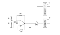
- the configuration of the sensor output device 1 according to the embodiment of the present invention is shown in FIG.
- the sensor output device 1 is composed of an oscillation circuit unit 5, a waveform adjustment unit 7, a waveform analysis unit 10, a frequency correction unit 20, and a specific unit 30.
- the oscillation circuit unit 5 is a general-purpose oscillation circuit composed of a resistor RB as a first impedance unit, a capacitor CA as a second impedance unit, and a comparator.
- the resistance RB for measurement corresponds to a part of the sensor made of pressure-sensitive conductive rubber, and the resistance changes according to the pressure applied to the sensor.
- the reference resistor RA is arranged in the vicinity of the resistor RB.
- the accuracy of this reference resistor RA against temperature changes is ⁇ 5 ⁇ 10 -6 / ° C, which is higher than that of the resistor RB made of pressure-sensitive conductive rubber. That of the capacitor CA was ⁇ 60 ⁇ 10-6 / ° C.
- the measurement resistor RB and the reference resistor RA are switched by the switch SW1 as a switching unit.
- the state of the oscillation circuit unit 5 in which the resistor RB is selected is the measurement mode
- the state of the oscillation circuit unit 5 in which the reference resistor RA is selected is the reference mode.
- an RC circuit was adopted as the oscillation circuit, but if you are a skilled person, you can select at least two impedance elements consisting of a resistor, a capacitor, and a coil, or a configuration that combines an inverter or NAND gate as shown in FIG. It can be easily assumed that an oscillator circuit can be constructed.
- the waveform adjusting unit 7 changes the waveform (rectangular wave) between the output of the measurement mode and the output of the reference mode.
- the amplitude of the output waveform is changed by switching the switch SW2 in synchronization with the switch SW1.
- the waveform analysis unit 10 specifies the frequency of the square wave. That is, the number of clocks from the rising edge of the rectangular wave to the falling edge is counted. It is assumed that 1 MHz or more is used as the clock. Since the time of a square wave (that is, 1/2 wavelength) is specified from the number of clocks, the frequency can be calculated. Of course, the number of clocks included in a plurality of consecutive rectangular waves may be counted.
- the frequency is stored in the frequency storage unit 23 of the frequency correction unit 20 as the output correction unit. Since the output of the waveform analysis unit 10 is merely frequency-related data, it is not possible to specify from the data alone whether it is derived from the measurement mode or the reference mode. Therefore, in this example, the switching timing (time t1) of the switch SW1 is controlled by a signal from the timing generation unit 21. The timing (time t1) at which the switching signal is output from the timing generation unit 21 is sent to the frequency storage unit 23, and is stored in association with the data sent from the waveform analysis unit 10. As a result, the data related to the frequency stored in the frequency storage unit 23 is associated with the time obtained.
- the frequency subtraction unit 25 subtracts the frequency (time t2) in the reference mode immediately after switching the switch SW1 from the frequency (time t1) in the measurement mode. Then, the frequency (time t4) in the reference mode immediately after the switch SW1 is switched again is subtracted from the frequency (time t3) in the measurement mode immediately after the switch SW1 is switched. After that, this is repeated.
- the identification unit 30 identifies the pressure change by comparing the frequency change corrected by the frequency correction unit 20 with the calibration data obtained in advance.
- the identified pressure change that is, the change in the characteristics of the sensor object, is presented to the observer through a monitor (not shown).
- the circuit of FIG. 2 has a small number of parts and can be miniaturized. If the strain gauge used in many applications is used as a resistor RB and integrated with the miniaturized circuit according to the present invention, the lead wire of the strain gauge can be shortened and highly accurate strain measurement becomes possible. Become. The difficulty in the measurement using the strain gauge is that the measurement result is disturbed by the change in the resistance value generated in the lead wire due to the change in the environmental temperature and the influence of the external noise superimposed on the lead wire.
- the length of the lead wire can be reduced to about several cm or less, the above-mentioned difficulty can be solved and high-precision measurement can be performed. If the measurement target is a conductor, if the entire circuit integrated with the strain gauge is covered with a conductor, including the lead wire, the influence of external noise will be completely eliminated and the strain will be measured with higher accuracy. Can be done.
- the resistance side is responsible for the sensor function, but the capacitor may be responsible for the sensor function (see FIG. 3).
- elements having the same functions as those in FIG. 2 are designated by the same reference numerals, and the description thereof will be partially omitted.
- the reference capacitor CA and the measurement capacitor CB are switched by the switch SW101 in the oscillation circuit unit 105.
- the oscillation circuit unit 205 for the measurement mode (first oscillation circuit, measurement waveform output unit) and the oscillation circuit unit 305 for the reference mode (second oscillation circuit, reference waveform output unit) are separate. It is a body, and a waveform analysis unit 10 is attached to each body.
- the output timing of the oscillation circuit units 205 and 305 is controlled by the timing signal input from the timing generation unit 21 to the switches SW201 and SW301. The time is specified and used for frequency correction in the frequency correction unit.
- SW1 selects two states, a measurement mode and a reference mode, but it is preferable to further include a pause mode.
- this hibernation mode no power is supplied to either the reference resistor RA or the resistor RB. By providing such a hibernation mode, power consumption can be reduced.
- FIG. 5 shows the configuration of the sensor output device of another embodiment.
- an oscillator circuit is composed of an inverter for a digital circuit (for example, TC74HC04 manufactured by Toshiba) and a NAND gate (for example, TC74HC00 manufactured by Toshiba), and a three-state buffer is set in the switch SW3 for switching between the measurement mode and the reference mode.
- TC74HC126 or TC74HC125 manufactured by Toshiba can be used.
- a reference mode for activating the reference resistor RA and a measurement mode for activating the resistor RB can be selected based on the signal from the timing generation unit 21. Further, if the L level signal from the timing generation circuit is input to the NAND gate, the output of the gate becomes the L level, the oscillation is stopped, the hibernation mode is set, and the current consumption at DC5V becomes 20 ⁇ A or less.
- the resistance value of the reference resistance RA is also 120 ⁇ , and when the power supply is DC5V, the reference resistance RA and the resistance RB have a maximum of 41.7mA. Current flows. Therefore, the hibernation mode is selected so that the circuit is not oscillated during unnecessary time and unnecessary current is not passed through the reference resistor RA and the resistor RB.
- the measurement accuracy is improved by adopting the three-state buffer as the switch SW3.
- the ON resistance does not always become a constant value, but if the three-state buffer is adopted as the switch SW3, the ON resistance becomes constant, so that the measurement accuracy is considered to be improved. ..
- FIG. 6 shows the configuration of the sensor output device of another embodiment.
- the reference resistor RA that uses a comparator that suppresses zero drift and executes the reference mode is omitted.
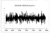
- the change in resistance value obtained from the frequency change of such a device was about ⁇ 80 ppm with respect to the temperature change of ⁇ 5 ° C. (see FIG. 7).
- FIG. 8 shows the difference in resistance value change. It can be seen that the standard deviation of the 50 data at the beginning of FIG. 8 is a little less than 1.0 ⁇ 10-6 , and the rate of change in resistance in a short time is about ⁇ 1.0 ⁇ 10-6.
- the amplitude of the diurnal change in frequency is about 160 ppm, and a highly accurate measurement result can be obtained. This is due to the use of a comparator that suppresses zero drift.
- a comparator (TS3011) manufactured by Kus Co., Ltd. was used for STMicroelectronics.
- An oscillation circuit can be configured even when a Schmitt trigger input inverter for digital circuits (for example, TC74HC14 manufactured by Toshiba) is used, but the inverter has a more uncertain signal high / low switching threshold than the comparator, so subtle temperature changes occur.
- the threshold value of the inverter itself may be affected and the measurement result may be disturbed.
- the comparator that suppresses zero drift it is considered that the threshold value is stable and the measurement result is not easily disturbed.
- an operational amplifier or a zero drift amplifier can be used instead of the comparator.
- more power saving can be achieved by using a low power consumption comparator, an operational amplifier, and a zero drift amplifier, and if a sleep mode is provided, it can be oscillated only when necessary. Further power saving can be achieved.
- the circuit of FIG. 6 since the parts necessary for selecting the reference resistor are omitted, the circuit can be miniaturized, and it is less affected by external noise, and there is an advantage that the space at the time of assembling or the like can be omitted.
Landscapes
- Physics & Mathematics (AREA)
- General Physics & Mathematics (AREA)
- Measuring Fluid Pressure (AREA)
Abstract
This output device for an oscillation circuit-type sensor improves measurement precision. This output device for a sensor comprises a first identification unit that analyzes an output waveform of a first oscillation circuit section and identifies a characteristic of a sensor target, the first oscillation circuit section being provided with a first impedance and a second impedance of a different type than the first impedance, and the first impedance or the second impedance having a sensor function. The greater external environmental change sensitivity among the external environmental change sensitivity of the first impedance and the external environmental change sensitivity of the second impedance, and the external environmental change sensitivity of the characteristic identified by the first identification unit are roughly equivalent.
Description
本発明はセンサ用出力装置の改良に関する。
The present invention relates to an improvement of an output device for a sensor.
センサは物理現象や化学現象の変化を電圧、電流その他の電気量の変化に変換する。
かかるセンサの変化は微弱であるため、センサにはセンサ用出力装置が付設されて、センサにおける電気量の変化を増幅若しくは変換して汎用的な検出装置で検出可能とする。
例えば、圧力の変化を電気抵抗の変化に変換するセンサ(感圧導電性ゴムなど)に付設されて、その電気抵抗の変化を増幅するセンサ用出力装置として、ホイートストンブリッジ回路の利用が知られている。
特許文献1には、電気抵抗(以下、単に「抵抗」ということがある)の変化に対応する出力装置として発振回路を用いるものが開示されている。このセンサ用出力装置では、発振回路を構成する抵抗(R)とコンデンサ(C)において、抵抗の部分をセンサとして、その抵抗の変化を周波数の変化として出力する。 Sensors convert changes in physical and chemical phenomena into changes in voltage, current, and other amounts of electricity.
Since such a change in the sensor is weak, a sensor output device is attached to the sensor to amplify or convert the change in the amount of electricity in the sensor so that it can be detected by a general-purpose detection device.
For example, the use of a Wheatstone bridge circuit is known as an output device for a sensor that is attached to a sensor that converts a change in pressure into a change in electrical resistance (such as pressure-sensitive conductive rubber) and amplifies the change in electrical resistance. There is.
Patent Document 1 discloses a device that uses an oscillation circuit as an output device that responds to changes in electrical resistance (hereinafter, may be simply referred to as "resistance"). In this sensor output device, in the resistance (R) and the capacitor (C) constituting the oscillation circuit, the resistance portion is used as a sensor, and the change in the resistance is output as the change in frequency.
かかるセンサの変化は微弱であるため、センサにはセンサ用出力装置が付設されて、センサにおける電気量の変化を増幅若しくは変換して汎用的な検出装置で検出可能とする。
例えば、圧力の変化を電気抵抗の変化に変換するセンサ(感圧導電性ゴムなど)に付設されて、その電気抵抗の変化を増幅するセンサ用出力装置として、ホイートストンブリッジ回路の利用が知られている。
特許文献1には、電気抵抗(以下、単に「抵抗」ということがある)の変化に対応する出力装置として発振回路を用いるものが開示されている。このセンサ用出力装置では、発振回路を構成する抵抗(R)とコンデンサ(C)において、抵抗の部分をセンサとして、その抵抗の変化を周波数の変化として出力する。 Sensors convert changes in physical and chemical phenomena into changes in voltage, current, and other amounts of electricity.
Since such a change in the sensor is weak, a sensor output device is attached to the sensor to amplify or convert the change in the amount of electricity in the sensor so that it can be detected by a general-purpose detection device.
For example, the use of a Wheatstone bridge circuit is known as an output device for a sensor that is attached to a sensor that converts a change in pressure into a change in electrical resistance (such as pressure-sensitive conductive rubber) and amplifies the change in electrical resistance. There is.
特許文献1に開示の発振回路型のセンサ用出力装置では、コンデンサの精度として±0.1~0.2%のものを利用することにより、高精度な測定が可能であることが示唆されている。ここにコンデンサの精度とは、温度などの外部環境の変化に応じて変化する容量の割合を指す。換言すれば、この精度の高いものは、外部環境の変化に応じる容量の変化(感度)が小さいものいう。このことを、この明細書では外部環境変化感度が小さいと説明することがある。
このセンサ用出力装置においてどの程度の測定精度が得られているのか不明である。
特に、コンデンサの精度が抵抗とほぼ等しい程度まで高いものとなったとき、例えば、両者の精度が10-5~10-6/℃となったとき、センサ用出力装置の測定精度がどの程度になるかは不明であった。 It is suggested that in the oscillation circuit type sensor output device disclosed inPatent Document 1, high-precision measurement is possible by using a capacitor with an accuracy of ± 0.1 to 0.2%. Here, the accuracy of a capacitor refers to the ratio of capacitance that changes in response to changes in the external environment such as temperature. In other words, the one with high accuracy means that the change (sensitivity) of the capacity in response to the change of the external environment is small. This may be explained in this specification as having a low sensitivity to changes in the external environment.
It is unclear how much measurement accuracy is obtained with this sensor output device.
In particular, when the accuracy of the capacitor becomes as high as the resistance, for example, when the accuracy of both becomes 10-5 to 10-6 / ° C, how much is the measurement accuracy of the output device for the sensor? It was unclear if it would be.
このセンサ用出力装置においてどの程度の測定精度が得られているのか不明である。
特に、コンデンサの精度が抵抗とほぼ等しい程度まで高いものとなったとき、例えば、両者の精度が10-5~10-6/℃となったとき、センサ用出力装置の測定精度がどの程度になるかは不明であった。 It is suggested that in the oscillation circuit type sensor output device disclosed in
It is unclear how much measurement accuracy is obtained with this sensor output device.
In particular, when the accuracy of the capacitor becomes as high as the resistance, for example, when the accuracy of both becomes 10-5 to 10-6 / ° C, how much is the measurement accuracy of the output device for the sensor? It was unclear if it would be.
本発明者らは、かかる発振回路型のセンサ用出力装置を用いた測定を行ってきたところ、その測定精度(外部環境変化感度)がコンデンサ自体の精度(外部環境変化感度)と等しくなる(外部環境変化感度が小さくなる)ことに気がついた。ここに等しいとは、当業者が理解できる範囲で誤差が含まれる。
図1に示すように、発振回路型のセンサ用出力装置の測定の精度は±1500×10-6/℃を指した。このときのコンデンサの精度は±60.0×10-6/℃、抵抗の精度(定格)は±5×10-6/℃であった。
なお、図1において縦軸(左側)は周波数の変化率を表し、横軸は時間の経過を指す。 When the present inventors have performed measurements using such an oscillator circuit type sensor output device, the measurement accuracy (external environment change sensitivity) becomes equal to the accuracy of the capacitor itself (external environment change sensitivity) (external). I noticed that the sensitivity to environmental changes decreases). Equal here includes errors to the extent that those skilled in the art can understand.
As shown in FIG. 1, the measurement accuracy of the oscillator circuit type sensor output device pointed to ± 1500 × 10-6 / ° C. At this time, the accuracy of the capacitor was ± 60.0 × 10⁻⁶ / ° C, and the accuracy (rating) of the resistor was ± 5 × 10⁻⁶ / ° C.
In FIG. 1, the vertical axis (left side) represents the rate of change in frequency, and the horizontal axis represents the passage of time.
このように、高い精度を有する抵抗とコンデンサと選択することにより、発振回路型のセンサ用出力装置も高い精度となることがわかる。換言すれば、単純な回路構成で高精度の出力が可能になった。かかる発振回路は消費電力も小さいのでセンサ用出力装置の用途が広がる。
図1に従って詳しい説明をする。筆者らが実験した発振回路型のセンサ用出力装置の出力の日周変化の大きさは図1の縦軸で示すように約8℃の変化に対して±1500×10-6であった(図では周波数の変化の比率に換算して記載し、単位は10-6である)。この実験時の回路のコンデンサの精度は±60×10-6/℃、抵抗の精度(定格)は±5×10-6/℃であった。図1において横軸は時間の経過を指す。
なお、図1のデータは周波数を直接測定したのではなく、周波数を分周して得た分周周期を10MHzのクロックでカウントして得た結果であり、かかる測定精度を達成するためには、センサ用出力装置の出力する波形の変化を1MHz以上のクロックで分析する。 As described above, it can be seen that the oscillator circuit type sensor output device also has high accuracy by selecting the resistor and the capacitor having high accuracy. In other words, high-precision output has become possible with a simple circuit configuration. Since such an oscillation circuit consumes less power, the application of the sensor output device is expanded.
A detailed explanation will be given according to FIG. As shown by the vertical axis in FIG. 1, the magnitude of the diurnal change in the output of the oscillator circuit type sensor output device that the authors experimented with was ± 1500 × 10-6 with respect to a change of about 8 ° C. ( In the figure, it is converted into the rate of change in frequency, and the unit is 10-6 ). The accuracy of the capacitor in the circuit at the time of this experiment was ± 60 × 10-6 / ° C, and the accuracy (rated) of the resistor was ± 5 × 10⁻⁶ / ° C. In FIG. 1, the horizontal axis indicates the passage of time.
The data in FIG. 1 is not the result of directly measuring the frequency, but the result obtained by counting the frequency division period obtained by dividing the frequency with a clock of 10 MHz, and in order to achieve such measurement accuracy. , The change of the waveform output by the sensor output device is analyzed with a clock of 1 MHz or more.
図1において、発振回路型のセンサ用出力装置の出力変化の比率が大きな日周変化をしていることから、出力周波数は温度の影響で変化することがわかる。この発明の他の目的は、かかる発振回路型のセンサ用出力装置の精度の更なる向上を目指すことにある。
本発明者らは、図1の例においては、センサとなる抵抗RBの近傍に基準抵抗RAを配置し、この基準抵抗RAを用いて発振回路(第2の発振回路部)を構成した。この第2の発振回路部は第1の発振回路部と、抵抗RBの部分を除いて、同一とする(図2,4参照)。基準抵抗RAを備える発振回路(第2の発振回路部)を基準波形出力部ということがある。他方、センサとなる抵抗RBを備えた発振回路(第1の発振回路部)を測定波形出力部ということがある。
この基準波形出力部は、センサとなる抵抗RBを備える測定波形出力部と独立していても(図4参照)、抵抗部分以外で共通化されていてもよい(図2参照)。抵抗RBと基準抵抗RAとを近接させること、及び部品点数削減の見地から、後者(図2)の方が好ましい。 In FIG. 1, since the ratio of the output change of the oscillator circuit type sensor output device has a large diurnal change, it can be seen that the output frequency changes under the influence of temperature. Another object of the present invention is to further improve the accuracy of such an oscillator circuit type sensor output device.
In the example of FIG. 1, the present inventors arranged a reference resistor RA in the vicinity of the resistor RB serving as a sensor, and constructed an oscillation circuit (second oscillation circuit section) using the reference resistor RA. The second oscillation circuit section is the same as the first oscillation circuit section except for the resistor RB portion (see FIGS. 2 and 4). An oscillation circuit (second oscillation circuit section) provided with a reference resistor RA may be referred to as a reference waveform output section. On the other hand, an oscillation circuit (first oscillation circuit unit) provided with a resistor RB that serves as a sensor may be referred to as a measurement waveform output unit.
This reference waveform output unit may be independent of the measurement waveform output unit including the resistance RB serving as a sensor (see FIG. 4), or may be shared by other than the resistance portion (see FIG. 2). The latter (FIG. 2) is preferable from the viewpoint of bringing the resistor RB and the reference resistor RA close to each other and reducing the number of parts.
図1の例では、測定波形出力部からの出力と基準波形出力部からの出力とを0.45秒ごとに切り替えて、後者で前者を補正した。即ち、前者の出力から後者の出力を差し引いた。そして、これを繰り返す。その結果、チャート上の補正後の日周変化の大きさは約8℃の変化に対し±10×10-6以下の振幅となった。つまり、差分処理の前の値である振幅±1500×10-6が2桁以上小さな振幅±10×10-6になり、測定精度が向上したことになる。
上記においては、測定波形出力部からの出力と基準波形出力部からの出力とに時間差ができないようにして、補正の精度向上を狙っている。求められる精度によっては、両者の間に時間差があってもよいが、その時間差は少なくとも10秒以内、更に好ましくは1秒以内とする。電子回路で生じるドリフトを取り除くためには、時間差が少なければより効果的である。 In the example of FIG. 1, the output from the measurement waveform output unit and the output from the reference waveform output unit are switched every 0.45 seconds, and the former is corrected by the latter. That is, the output of the latter was subtracted from the output of the former. And this is repeated. As a result, the magnitude of the corrected diurnal change on the chart was ± 10 × 10-6 or less with respect to the change of about 8 ° C. That is, the amplitude ± 1500 × 10 -6 is a previous value of the difference processing becomes smaller amplitude ± 10 × 10 -6 2 digits or more, so that the measurement accuracy is improved.
In the above, the aim is to improve the accuracy of correction by preventing a time difference between the output from the measurement waveform output unit and the output from the reference waveform output unit. Depending on the required accuracy, there may be a time difference between the two, but the time difference is at least 10 seconds or less, more preferably 1 second or less. It is more effective if the time difference is small in order to eliminate the drift generated in the electronic circuit.
測定波形出力部や基準波形出力部からの出力は矩形波とすることが好ましい。矩形波の立ち上がり部分及び/又は立下り部分を使うことにより、その周波数を特定し易いからである。
測定波形出力部の出力波形は、波形解析部10において、一つの矩形波に含まれるクロック数をカウントする。これにより、1/2波長の時間が特定され、もって、周波数が演算される。
基準波形出力部からの出力波形も同様に処理される。測定波形出力部からの出力波形と基準波形出力部からの出力波形とを峻別するため、両者の振幅や1波長に占める矩形波の比率を変えることができる。
周波数を特定するため、1/2波長以上の波形を用いることもできるし、分周回路を設けて出力周波数を低くすることもできる。 The output from the measurement waveform output unit and the reference waveform output unit is preferably a rectangular wave. This is because it is easy to specify the frequency by using the rising portion and / or the falling portion of the rectangular wave.
For the output waveform of the measurement waveform output unit, thewaveform analysis unit 10 counts the number of clocks included in one square wave. As a result, the time of 1/2 wavelength is specified, and the frequency is calculated.
The output waveform from the reference waveform output unit is also processed in the same manner. Since the output waveform from the measurement waveform output unit and the output waveform from the reference waveform output unit are distinguished, the amplitude of both and the ratio of the rectangular wave to one wavelength can be changed.
In order to specify the frequency, a waveform having a wavelength of 1/2 or more can be used, or a frequency dividing circuit can be provided to lower the output frequency.
測定波形出力部の出力波形は、波形解析部10において、一つの矩形波に含まれるクロック数をカウントする。これにより、1/2波長の時間が特定され、もって、周波数が演算される。
基準波形出力部からの出力波形も同様に処理される。測定波形出力部からの出力波形と基準波形出力部からの出力波形とを峻別するため、両者の振幅や1波長に占める矩形波の比率を変えることができる。
周波数を特定するため、1/2波長以上の波形を用いることもできるし、分周回路を設けて出力周波数を低くすることもできる。 The output from the measurement waveform output unit and the reference waveform output unit is preferably a rectangular wave. This is because it is easy to specify the frequency by using the rising portion and / or the falling portion of the rectangular wave.
For the output waveform of the measurement waveform output unit, the
The output waveform from the reference waveform output unit is also processed in the same manner. Since the output waveform from the measurement waveform output unit and the output waveform from the reference waveform output unit are distinguished, the amplitude of both and the ratio of the rectangular wave to one wavelength can be changed.
In order to specify the frequency, a waveform having a wavelength of 1/2 or more can be used, or a frequency dividing circuit can be provided to lower the output frequency.
上記のように、波形解析部10の出力は周波数なるデジタルデータとなる。よって、かかる出力の増幅は簡易に行われ、伝送時に重畳するノイズを簡単に除去できる。
一つの波形解析部10へ測定波形出力部の出力波及び基準波形出力部の出力波がともに入力されたとき、波形解析部10からの出力は単に周波数を表すデジタルデータであるため、いずれの出力波によるものかを判定できない。
そこで、測定波形出力部からの出力波形を波形解析部10に入力する第1のタイミング(例えば時刻t1)を決定する信号を周波数補正部(出力補正部)20のタイミング発生部21から入力する。周波数減算部25はその第1のタイミング(時刻t1)を保存する。同様に基準波形出力部からの出力波形を波形解析部10に入力する第2のタイミング(例えば時刻t2)を決定する信号をタイミング発生部21から入力する。周波数減算部25はその第2のタイミング(時刻t2)を保存する。 As described above, the output of thewaveform analysis unit 10 is digital data having a frequency. Therefore, such output amplification is easily performed, and noise superimposed during transmission can be easily removed.
When both the output wave of the measurement waveform output unit and the output wave of the reference waveform output unit are input to onewaveform analysis unit 10, the output from the waveform analysis unit 10 is simply digital data representing the frequency, so any output. It cannot be determined whether it is due to a wave.
Therefore, a signal for determining the first timing (for example, time t1) for inputting the output waveform from the measurement waveform output unit to thewaveform analysis unit 10 is input from the timing generation unit 21 of the frequency correction unit (output correction unit) 20. The frequency subtraction unit 25 stores the first timing (time t1). Similarly, a signal for determining a second timing (for example, time t2) for inputting the output waveform from the reference waveform output unit to the waveform analysis unit 10 is input from the timing generation unit 21. The frequency subtraction unit 25 stores the second timing (time t2).
一つの波形解析部10へ測定波形出力部の出力波及び基準波形出力部の出力波がともに入力されたとき、波形解析部10からの出力は単に周波数を表すデジタルデータであるため、いずれの出力波によるものかを判定できない。
そこで、測定波形出力部からの出力波形を波形解析部10に入力する第1のタイミング(例えば時刻t1)を決定する信号を周波数補正部(出力補正部)20のタイミング発生部21から入力する。周波数減算部25はその第1のタイミング(時刻t1)を保存する。同様に基準波形出力部からの出力波形を波形解析部10に入力する第2のタイミング(例えば時刻t2)を決定する信号をタイミング発生部21から入力する。周波数減算部25はその第2のタイミング(時刻t2)を保存する。 As described above, the output of the
When both the output wave of the measurement waveform output unit and the output wave of the reference waveform output unit are input to one
Therefore, a signal for determining the first timing (for example, time t1) for inputting the output waveform from the measurement waveform output unit to the
これにより、共通した時間軸において測定波形出力部からの出力波形の位置(時系列配置)と基準波形出力部からの出力波形の位置(時系列配置)が定められる。
タイミング発生部からの入力信号や測定波形の出力信号は、フォトカプラー等の絶縁型デバイスを介する形態が好適で、かかる形態であれば発振回路が外部ノイズの影響を受け難くなる。 As a result, the position of the output waveform from the measurement waveform output unit (time series arrangement) and the position of the output waveform from the reference waveform output unit (time series arrangement) are determined on a common time axis.
The input signal from the timing generator and the output signal of the measurement waveform are preferably in the form of passing through an isolated device such as a photocoupler, and in such a form, the oscillation circuit is less likely to be affected by external noise.
周波数補正部20では、第2のタイミングから得られた基準波形出力部からの出力波形に基づく周波数を基準にして、第1のタイミングで得られた測定波形出力部の出力波形に基づく周波数を補正する。補正の方法として、図1の場合は、周波数減算部25により測定波形出力部からの出力波形に基づく周波数から基準波形出力部からの出力波形に基づく周波数を減算する。
図1の例では、第1のタイミングで得た周波数を直後の第2のタイミングで得られた周波数で補正している。勿論、第1のタイミングで得られた周波数を、直前の第2のタイミングで得られた周波数で補正してもよい。 Thefrequency correction unit 20 corrects the frequency based on the output waveform of the measurement waveform output unit obtained at the first timing with reference to the frequency based on the output waveform from the reference waveform output unit obtained from the second timing. do. As a correction method, in the case of FIG. 1, the frequency subtraction unit 25 subtracts the frequency based on the output waveform from the reference waveform output unit from the frequency based on the output waveform from the measurement waveform output unit.
In the example of FIG. 1, the frequency obtained at the first timing is corrected by the frequency obtained at the second timing immediately after. Of course, the frequency obtained at the first timing may be corrected by the frequency obtained at the second timing immediately before.
図1の例では、第1のタイミングで得た周波数を直後の第2のタイミングで得られた周波数で補正している。勿論、第1のタイミングで得られた周波数を、直前の第2のタイミングで得られた周波数で補正してもよい。 The
In the example of FIG. 1, the frequency obtained at the first timing is corrected by the frequency obtained at the second timing immediately after. Of course, the frequency obtained at the first timing may be corrected by the frequency obtained at the second timing immediately before.
この発明の実施形態のセンサ用出力装置1の構成を図2に示す。
このセンサ用出力装置1は発振回路部5、波形調整部7、波形解析部10、周波数補正部20及び特定部30から構成される。
発振回路部5は第1のインピーダンス部として抵抗RB、第2のインピーダンス部としてのキャパシタ(コンデンサ)CA及びコンパレータとから構成される汎用的な発振回路である。測定用の抵抗RBは感圧導電性ゴムからなるセンサの一部がこれに該当し、センサ加えられた圧力に応じてその抵抗が変化する。
この発振回路部5では、この抵抗RBに近接して基準抵抗RAを配置した。この基準抵抗RAの温度変化に対する精度(外部環境変化感度)は±5×10⁻⁶/℃であり、その精度は感圧導電性ゴムからなる抵抗RBより高い。コンデンサCAのそれは±60×10-6/℃であった。測定用の抵抗RBと基準抵抗RAは切替部としてのスイッチSW1により切り替えられる。 The configuration of thesensor output device 1 according to the embodiment of the present invention is shown in FIG.
Thesensor output device 1 is composed of an oscillation circuit unit 5, a waveform adjustment unit 7, a waveform analysis unit 10, a frequency correction unit 20, and a specific unit 30.
Theoscillation circuit unit 5 is a general-purpose oscillation circuit composed of a resistor RB as a first impedance unit, a capacitor CA as a second impedance unit, and a comparator. The resistance RB for measurement corresponds to a part of the sensor made of pressure-sensitive conductive rubber, and the resistance changes according to the pressure applied to the sensor.
In theoscillation circuit unit 5, the reference resistor RA is arranged in the vicinity of the resistor RB. The accuracy of this reference resistor RA against temperature changes (external environment change sensitivity) is ± 5 × 10 -6 / ° C, which is higher than that of the resistor RB made of pressure-sensitive conductive rubber. That of the capacitor CA was ± 60 × 10-6 / ° C. The measurement resistor RB and the reference resistor RA are switched by the switch SW1 as a switching unit.
このセンサ用出力装置1は発振回路部5、波形調整部7、波形解析部10、周波数補正部20及び特定部30から構成される。
発振回路部5は第1のインピーダンス部として抵抗RB、第2のインピーダンス部としてのキャパシタ(コンデンサ)CA及びコンパレータとから構成される汎用的な発振回路である。測定用の抵抗RBは感圧導電性ゴムからなるセンサの一部がこれに該当し、センサ加えられた圧力に応じてその抵抗が変化する。
この発振回路部5では、この抵抗RBに近接して基準抵抗RAを配置した。この基準抵抗RAの温度変化に対する精度(外部環境変化感度)は±5×10⁻⁶/℃であり、その精度は感圧導電性ゴムからなる抵抗RBより高い。コンデンサCAのそれは±60×10-6/℃であった。測定用の抵抗RBと基準抵抗RAは切替部としてのスイッチSW1により切り替えられる。 The configuration of the
The
The
In the
抵抗RBを選択した発振回路部5の状態が測定モードであり、基準抵抗RAを選択した発振回路部5の状態が基準モードである。
この例では発振回路としてRC回路を採用したが、当業者であれば図5で示すようなインバータやNANDゲートを組み合わせる構成や、抵抗、コンデンサ及びコイルからなるインピーダンス要素の少なくとも2つを選択して発振回路を構築できることは容易に想定できよう。 The state of theoscillation circuit unit 5 in which the resistor RB is selected is the measurement mode, and the state of the oscillation circuit unit 5 in which the reference resistor RA is selected is the reference mode.
In this example, an RC circuit was adopted as the oscillation circuit, but if you are a skilled person, you can select at least two impedance elements consisting of a resistor, a capacitor, and a coil, or a configuration that combines an inverter or NAND gate as shown in FIG. It can be easily assumed that an oscillator circuit can be constructed.
この例では発振回路としてRC回路を採用したが、当業者であれば図5で示すようなインバータやNANDゲートを組み合わせる構成や、抵抗、コンデンサ及びコイルからなるインピーダンス要素の少なくとも2つを選択して発振回路を構築できることは容易に想定できよう。 The state of the
In this example, an RC circuit was adopted as the oscillation circuit, but if you are a skilled person, you can select at least two impedance elements consisting of a resistor, a capacitor, and a coil, or a configuration that combines an inverter or NAND gate as shown in FIG. It can be easily assumed that an oscillator circuit can be constructed.
波形調整部7は、測定モードの出力と基準モードの出力との波形(矩形波)に変化を与える。この例では、スイッチSW1に同期させてスイッチSW2を切り替えることで、それぞれ出力波形の振幅に変化を与えている。
波形解析部10は矩形波の周波数を特定する。即ち、矩形波の立ち上がりから立下りまでのクロック数をカウントする。クロックとしては1MHz以上を用いるものとする。クロック数から矩形波(即ち1/2波長)の時間が特定されるので、周波数が計算できる。勿論、連続した複数の矩形波に含まれるクロック数をカウントしてもよい。 Thewaveform adjusting unit 7 changes the waveform (rectangular wave) between the output of the measurement mode and the output of the reference mode. In this example, the amplitude of the output waveform is changed by switching the switch SW2 in synchronization with the switch SW1.
Thewaveform analysis unit 10 specifies the frequency of the square wave. That is, the number of clocks from the rising edge of the rectangular wave to the falling edge is counted. It is assumed that 1 MHz or more is used as the clock. Since the time of a square wave (that is, 1/2 wavelength) is specified from the number of clocks, the frequency can be calculated. Of course, the number of clocks included in a plurality of consecutive rectangular waves may be counted.
波形解析部10は矩形波の周波数を特定する。即ち、矩形波の立ち上がりから立下りまでのクロック数をカウントする。クロックとしては1MHz以上を用いるものとする。クロック数から矩形波(即ち1/2波長)の時間が特定されるので、周波数が計算できる。勿論、連続した複数の矩形波に含まれるクロック数をカウントしてもよい。 The
The
波形解析部10で特定されたデジタルデータとして周波数は出力補正部としての周波数補正部20の周波数保存部23に保存される。
波形解析部10の出力は単なる周波数に関するデータであるので、それが測定モードに由来するものか、若しくは基準モードに由来するものかを、データのみから特定することはできない。そこで、この例では、スイッチSW1の切替えのタイミング(時刻t1)をタイミング発生部21から信号で制御する。タイミング発生部21から切替信号を出力したタイミング(時刻t1)は周波数保存部23に送られて、波形解析部10から送られるデータに関連付けて保存される。これにより、周波数保存部23に保存される周波数に関するデータは、それが得らた時刻と紐づけられる。 As the digital data specified by thewaveform analysis unit 10, the frequency is stored in the frequency storage unit 23 of the frequency correction unit 20 as the output correction unit.
Since the output of thewaveform analysis unit 10 is merely frequency-related data, it is not possible to specify from the data alone whether it is derived from the measurement mode or the reference mode. Therefore, in this example, the switching timing (time t1) of the switch SW1 is controlled by a signal from the timing generation unit 21. The timing (time t1) at which the switching signal is output from the timing generation unit 21 is sent to the frequency storage unit 23, and is stored in association with the data sent from the waveform analysis unit 10. As a result, the data related to the frequency stored in the frequency storage unit 23 is associated with the time obtained.
波形解析部10の出力は単なる周波数に関するデータであるので、それが測定モードに由来するものか、若しくは基準モードに由来するものかを、データのみから特定することはできない。そこで、この例では、スイッチSW1の切替えのタイミング(時刻t1)をタイミング発生部21から信号で制御する。タイミング発生部21から切替信号を出力したタイミング(時刻t1)は周波数保存部23に送られて、波形解析部10から送られるデータに関連付けて保存される。これにより、周波数保存部23に保存される周波数に関するデータは、それが得らた時刻と紐づけられる。 As the digital data specified by the
Since the output of the
周波数減算部25は測定モードでの周波数(時刻t1)から、スイッチSW1を切り替えた直後での基準モードでの周波数(時刻t2)を減算する。そして、次にスイッチSW1を切り替えた直後の測定モードでの周波数(時刻t3)から、再度スイッチSW1を切り替えた直後の基準モードでの周波数(時刻t4)を減算する。以後、これを繰り返す。
The frequency subtraction unit 25 subtracts the frequency (time t2) in the reference mode immediately after switching the switch SW1 from the frequency (time t1) in the measurement mode. Then, the frequency (time t4) in the reference mode immediately after the switch SW1 is switched again is subtracted from the frequency (time t3) in the measurement mode immediately after the switch SW1 is switched. After that, this is repeated.
特定部30は、周波数補正部20で補正された周波数の変化を、予め求めておいた校正データに照らして、圧力変化を特定する。特定した圧力変化、即ちセンサ対象の特性の変化は図示しないモニタを介して観察者に提示される。
図2の回路は部品点数が少なく小型化ができる。多くの用途で使用されているひずみゲージを抵抗RBとして利用し、本発明による小型化した回路と一体化させれば、ひずみゲージのリード線を短くすることができ高精度のひずみ測定が可能になる。ひずみゲージを用いる測定における難点は、環境温度の変化に伴いリード線に生じる抵抗値の変化やリード線に重畳する外部ノイズの影響で測定結果が乱されることである。リード線の長さを数cm程度以下にできれば、上記の難点が解消され、高精度の測定ができる。なお、測定対象が導電体である場合はひずみゲージと一体化した回路全体を、リード線を含めて、導電体で覆う構成にすれば、外部ノイズの影響が皆無となり、より高精度のひずみ測定ができる。 Theidentification unit 30 identifies the pressure change by comparing the frequency change corrected by the frequency correction unit 20 with the calibration data obtained in advance. The identified pressure change, that is, the change in the characteristics of the sensor object, is presented to the observer through a monitor (not shown).
The circuit of FIG. 2 has a small number of parts and can be miniaturized. If the strain gauge used in many applications is used as a resistor RB and integrated with the miniaturized circuit according to the present invention, the lead wire of the strain gauge can be shortened and highly accurate strain measurement becomes possible. Become. The difficulty in the measurement using the strain gauge is that the measurement result is disturbed by the change in the resistance value generated in the lead wire due to the change in the environmental temperature and the influence of the external noise superimposed on the lead wire. If the length of the lead wire can be reduced to about several cm or less, the above-mentioned difficulty can be solved and high-precision measurement can be performed. If the measurement target is a conductor, if the entire circuit integrated with the strain gauge is covered with a conductor, including the lead wire, the influence of external noise will be completely eliminated and the strain will be measured with higher accuracy. Can be done.
図2の回路は部品点数が少なく小型化ができる。多くの用途で使用されているひずみゲージを抵抗RBとして利用し、本発明による小型化した回路と一体化させれば、ひずみゲージのリード線を短くすることができ高精度のひずみ測定が可能になる。ひずみゲージを用いる測定における難点は、環境温度の変化に伴いリード線に生じる抵抗値の変化やリード線に重畳する外部ノイズの影響で測定結果が乱されることである。リード線の長さを数cm程度以下にできれば、上記の難点が解消され、高精度の測定ができる。なお、測定対象が導電体である場合はひずみゲージと一体化した回路全体を、リード線を含めて、導電体で覆う構成にすれば、外部ノイズの影響が皆無となり、より高精度のひずみ測定ができる。 The
The circuit of FIG. 2 has a small number of parts and can be miniaturized. If the strain gauge used in many applications is used as a resistor RB and integrated with the miniaturized circuit according to the present invention, the lead wire of the strain gauge can be shortened and highly accurate strain measurement becomes possible. Become. The difficulty in the measurement using the strain gauge is that the measurement result is disturbed by the change in the resistance value generated in the lead wire due to the change in the environmental temperature and the influence of the external noise superimposed on the lead wire. If the length of the lead wire can be reduced to about several cm or less, the above-mentioned difficulty can be solved and high-precision measurement can be performed. If the measurement target is a conductor, if the entire circuit integrated with the strain gauge is covered with a conductor, including the lead wire, the influence of external noise will be completely eliminated and the strain will be measured with higher accuracy. Can be done.
図2の例では、抵抗側にセンサ機能を担わせたが、コンデンサにセンサ機能を担わせる場合もある(図3参照)。
図3において、図2と同じ機能を奏する要素には同一の符号を付してのその説明を部分的に省略する。
図3の例では、その発振回路部105において基準コンデンサCAと測定用のコンデンサCBとがスイッチSW101により切り替えられている。 In the example of FIG. 2, the resistance side is responsible for the sensor function, but the capacitor may be responsible for the sensor function (see FIG. 3).
In FIG. 3, elements having the same functions as those in FIG. 2 are designated by the same reference numerals, and the description thereof will be partially omitted.
In the example of FIG. 3, the reference capacitor CA and the measurement capacitor CB are switched by the switch SW101 in theoscillation circuit unit 105.
図3において、図2と同じ機能を奏する要素には同一の符号を付してのその説明を部分的に省略する。
図3の例では、その発振回路部105において基準コンデンサCAと測定用のコンデンサCBとがスイッチSW101により切り替えられている。 In the example of FIG. 2, the resistance side is responsible for the sensor function, but the capacitor may be responsible for the sensor function (see FIG. 3).
In FIG. 3, elements having the same functions as those in FIG. 2 are designated by the same reference numerals, and the description thereof will be partially omitted.
In the example of FIG. 3, the reference capacitor CA and the measurement capacitor CB are switched by the switch SW101 in the
他の実施形態のセンサ用出力装置の構成を図4に示す。
このセンサ用出力装置では測定モード用の発振回路部205(第1の発振回路、測定波形出力部)と基準モード用の発振回路部305(第2の発振回路、基準波形出力部)とが別体とされ、それぞれに波形解析部10が付設されている。
発振回路部205、305の出力のタイミングは、タイミング発生部21からスイッチSW201、SW301へ入力されるタイミング信号で制御される。その時刻が特定されて、周波数補正部における周波数の補正に用いられる。 The configuration of the sensor output device of another embodiment is shown in FIG.
In this sensor output device, theoscillation circuit unit 205 for the measurement mode (first oscillation circuit, measurement waveform output unit) and the oscillation circuit unit 305 for the reference mode (second oscillation circuit, reference waveform output unit) are separate. It is a body, and a waveform analysis unit 10 is attached to each body.
The output timing of the oscillation circuit units 205 and 305 is controlled by the timing signal input from the timing generation unit 21 to the switches SW201 and SW301. The time is specified and used for frequency correction in the frequency correction unit.
このセンサ用出力装置では測定モード用の発振回路部205(第1の発振回路、測定波形出力部)と基準モード用の発振回路部305(第2の発振回路、基準波形出力部)とが別体とされ、それぞれに波形解析部10が付設されている。
発振回路部205、305の出力のタイミングは、タイミング発生部21からスイッチSW201、SW301へ入力されるタイミング信号で制御される。その時刻が特定されて、周波数補正部における周波数の補正に用いられる。 The configuration of the sensor output device of another embodiment is shown in FIG.
In this sensor output device, the
The output timing of the
上記の例では、SW1は測定モードと基準モードとの2つの状態を選択しているが、さらに休止モードを備えることが好ましい。この休止モードでは基準抵抗RAにも抵抗RBにも電力は供給されない。かかる休止モードを設けることで、消費電力を削減できる。
In the above example, SW1 selects two states, a measurement mode and a reference mode, but it is preferable to further include a pause mode. In this hibernation mode, no power is supplied to either the reference resistor RA or the resistor RB. By providing such a hibernation mode, power consumption can be reduced.
図5には、他の実施形態のセンサ用出力装置の構成を示す。この例では、デジタル回路用のインバータ(例えば東芝製のTC74HC04)とNANDゲート(例えば東芝製のTC74HC00)で発振回路が構成されており、測定モードと基準モードとを切り替えるスイッチSW3に、スリーステートバッファを用いる。例えば、東芝製のTC74HC126やTC74HC125を用いることができる。
かかるスイッチSW3によれば、タイミング発生部21からの信号に基づき、基準抵抗RAを活性化する基準モード、抵抗RBを活性化する測定モードを選択できる。また、タイミング発生回路からのLレベルの信号をNANDゲートに入力すれば、ゲートの出力がLレベルになり発振が停止し、休止モードとなってDC5Vの時の消費電流が20μA以下になる。 FIG. 5 shows the configuration of the sensor output device of another embodiment. In this example, an oscillator circuit is composed of an inverter for a digital circuit (for example, TC74HC04 manufactured by Toshiba) and a NAND gate (for example, TC74HC00 manufactured by Toshiba), and a three-state buffer is set in the switch SW3 for switching between the measurement mode and the reference mode. Is used. For example, TC74HC126 or TC74HC125 manufactured by Toshiba can be used.
According to the switch SW3, a reference mode for activating the reference resistor RA and a measurement mode for activating the resistor RB can be selected based on the signal from thetiming generation unit 21. Further, if the L level signal from the timing generation circuit is input to the NAND gate, the output of the gate becomes the L level, the oscillation is stopped, the hibernation mode is set, and the current consumption at DC5V becomes 20 μA or less.
かかるスイッチSW3によれば、タイミング発生部21からの信号に基づき、基準抵抗RAを活性化する基準モード、抵抗RBを活性化する測定モードを選択できる。また、タイミング発生回路からのLレベルの信号をNANDゲートに入力すれば、ゲートの出力がLレベルになり発振が停止し、休止モードとなってDC5Vの時の消費電流が20μA以下になる。 FIG. 5 shows the configuration of the sensor output device of another embodiment. In this example, an oscillator circuit is composed of an inverter for a digital circuit (for example, TC74HC04 manufactured by Toshiba) and a NAND gate (for example, TC74HC00 manufactured by Toshiba), and a three-state buffer is set in the switch SW3 for switching between the measurement mode and the reference mode. Is used. For example, TC74HC126 or TC74HC125 manufactured by Toshiba can be used.
According to the switch SW3, a reference mode for activating the reference resistor RA and a measurement mode for activating the resistor RB can be selected based on the signal from the
例えば抵抗RBとして120Ωの抵抗値を有するひずみゲージが採用されるとき、基準抵抗RAの抵抗値も120Ωが採用されて、電源がDC5Vの場合、基準抵抗RAと抵抗RBには最大41.7mAの電流が流れる。そこで、休止モードを選択し、不要な時間には回路を発振させず、基準抵抗RA及び抵抗RBに無駄な電流を流すことを避ける。
For example, when a strain gauge having a resistance value of 120Ω is adopted as the resistance RB, the resistance value of the reference resistance RA is also 120Ω, and when the power supply is DC5V, the reference resistance RA and the resistance RB have a maximum of 41.7mA. Current flows. Therefore, the hibernation mode is selected so that the circuit is not oscillated during unnecessary time and unnecessary current is not passed through the reference resistor RA and the resistor RB.
さらには、本発明者らの検討によれば、スリーステートバッファをスイッチSW3として採用することにより、測定精度の向上もみられた。
図2~4で採用するアナログ式のスイッチSW1の場合はON抵抗が必ずしも一定値にならないが、スリーステートバッファをスイッチSW3として採用すればON抵抗が一定になるため、測定精度が向上すると考えられる。 Furthermore, according to the study by the present inventors, the measurement accuracy is improved by adopting the three-state buffer as the switch SW3.
In the case of the analog switch SW1 adopted in FIGS. 2 to 4, the ON resistance does not always become a constant value, but if the three-state buffer is adopted as the switch SW3, the ON resistance becomes constant, so that the measurement accuracy is considered to be improved. ..
図6には、他の実施形態のセンサ用出力装置の構成を示す。
この例では、ゼロドリフトを抑制したコンパレータを採用し基準モードを実行する基準抵抗RAが省略されている。
かかる装置の周波数変化から求めた抵抗値の変化は±5℃の温度変化に対して±80ppm程度となった(図7参照)。図8は、抵抗値変化の階差を示す。図8の先頭部分の50個のデータの標準偏差は1.0×10⁻⁶弱であり、短時間の抵抗変化率が±1.0×10⁻⁶程度であることがわかる。この例では、基準抵抗用の回路を省略しても周波数の日周変化の振幅が160ppm程度であり高精度の測定結果が得られた。これは、ゼロドリフトを抑制したコンパレータを用いたことによる。この例では、STマイクロエレクトロにクス社のコンパレータ(TS3011)を用いた。 FIG. 6 shows the configuration of the sensor output device of another embodiment.
In this example, the reference resistor RA that uses a comparator that suppresses zero drift and executes the reference mode is omitted.
The change in resistance value obtained from the frequency change of such a device was about ± 80 ppm with respect to the temperature change of ± 5 ° C. (see FIG. 7). FIG. 8 shows the difference in resistance value change. It can be seen that the standard deviation of the 50 data at the beginning of FIG. 8 is a little less than 1.0 × 10⁻⁶ , and the rate of change in resistance in a short time is about ± 1.0 × 10⁻⁶. In this example, even if the circuit for the reference resistor is omitted, the amplitude of the diurnal change in frequency is about 160 ppm, and a highly accurate measurement result can be obtained. This is due to the use of a comparator that suppresses zero drift. In this example, a comparator (TS3011) manufactured by Kus Co., Ltd. was used for STMicroelectronics.
デジタル回路用のシュミットトリガ入力のインバータ(例えば東芝製のTC74HC14)を用いる場合でも発振回路が構成できるが、インバータでは信号のハイ、ローの切り替え閾値がコンパレータより不確実なため、微妙な温度変化がインバータの閾値自体に影響を与え測定結果が乱れるおそれがある。これに対し、ゼロドリフトを抑制したコンパレータでは閾値が安定で測定結果が乱れにくいと考えられる。
An oscillation circuit can be configured even when a Schmitt trigger input inverter for digital circuits (for example, TC74HC14 manufactured by Toshiba) is used, but the inverter has a more uncertain signal high / low switching threshold than the comparator, so subtle temperature changes occur. The threshold value of the inverter itself may be affected and the measurement result may be disturbed. On the other hand, in the comparator that suppresses zero drift, it is considered that the threshold value is stable and the measurement result is not easily disturbed.
同様の見地から、コンパレータの代わりにオペレーショナルアンプやゼロドリフト・アンプを採用することもできる。図6の回路では、低消費電力の少ないコンパレータ、オペレーショナルアンプ、ゼロドリフト・アンプを使用すればより省電力が達成できるし、スリープ・モードを備えていれば必要な時だけ発振させることができ、更なる省電力が達成できる。
図6の回路では、基準抵抗の選択に必要な部品が省略されるので回路が小型化でき、外部ノイズの影響を受けにくくなり組み込み等の時のスペースを省略できるメリットがある。 From the same point of view, an operational amplifier or a zero drift amplifier can be used instead of the comparator. In the circuit of FIG. 6, more power saving can be achieved by using a low power consumption comparator, an operational amplifier, and a zero drift amplifier, and if a sleep mode is provided, it can be oscillated only when necessary. Further power saving can be achieved.
In the circuit of FIG. 6, since the parts necessary for selecting the reference resistor are omitted, the circuit can be miniaturized, and it is less affected by external noise, and there is an advantage that the space at the time of assembling or the like can be omitted.
この発明は、上記発明の実施の形態及び実施例の説明に何ら限定されるものではない。特許請求の範囲の記載を逸脱せず、当業者が容易に想到できる範囲で種々の変形態様もこの発明に含まれる。図2から図6の回路はすべてICチップにまとめることができることは当業者であれば容易に理解される。
The present invention is not limited to the description of the embodiments and examples of the above invention. Various modifications are also included in the present invention as long as those skilled in the art can easily conceive without departing from the description of the scope of claims. It is easily understood by those skilled in the art that all the circuits of FIGS. 2 to 6 can be integrated into an IC chip.
1 センサ用出力装置
5、105、205、305 発振回路部
7 波形調整部 1 Sensor output device 5, 105, 205, 305 Oscillation circuit unit 7 Waveform adjustment unit
5、105、205、305 発振回路部
7 波形調整部 1
Claims (15)
- 第1のインピーダンス及び該第1のインピーダンスと異なる種類の第2のインピーダンスを備えた第1の発振回路部であって、前記第1のインピーダンスと第2のインピーダンスの一方がセンサ機能を有する、
該第1の発振回路部の出力波形を解析してセンサ対象の特性を特定する第1の特定部、を備えるセンサ用出力装置であって、
第1のインピーダンスの外部環境変化感度及び第2のインピーダンスの外部環境変化感度において大きいものの外部環境変化感度と、前記第1の特定部で特定された特性の外部環境変化感度とが等しくなる、センサ用出力装置。 A first oscillation circuit unit having a first impedance and a second impedance of a type different from the first impedance, and one of the first impedance and the second impedance has a sensor function.
An output device for a sensor including a first specific unit that analyzes the output waveform of the first oscillation circuit unit and specifies the characteristics of the sensor target.
A sensor in which the external environment change sensitivity of the first impedance and the external environment change sensitivity of the second impedance are large, but the external environment change sensitivity is equal to the external environment change sensitivity of the characteristic specified in the first specific part. Output device for. - 前記特定部は、前記発振回路部の出力波形を、1MHz以上のクロックで解析する、請求項1に記載のセンサ用出力装置。 The sensor output device according to claim 1, wherein the specific unit analyzes the output waveform of the oscillation circuit unit with a clock of 1 MHz or more.
- 前記第1のインピーダンスは抵抗であり、前記第2のインピーダンスはキャパシタである、請求項1又は2に記載のセンサ用出力装置。 The sensor output device according to claim 1 or 2, wherein the first impedance is a resistor and the second impedance is a capacitor.
- 前記第1の発振回路部にはゼロドリフトが抑制されたコンパレータ、オペレーショナルアンプ又はゼロドリフト・アンプが使用される、請求項1~3のいずれかに記載のセンサ用出力装置。 The sensor output device according to any one of claims 1 to 3, wherein a comparator, an operational amplifier, or a zero drift amplifier in which zero drift is suppressed is used in the first oscillation circuit unit.
- 前記発振回路部の稼働を休止させるタイミング制御部が更に備えられる、請求項1~4のいずれかに記載のセンサ用出力装置。 The sensor output device according to any one of claims 1 to 4, further comprising a timing control unit for suspending the operation of the oscillation circuit unit.
- 前記第1の発振回路部は前記第1のインピーダンスと同種の第1-1のインピーダンス又は前記第2のインピーダンスと同種の第2-1のインピーダンスを備え、
該第1-1のインピーダンスは前記センサ機能を有する第1のインピーダンスより小さい外部環境変化感度を有し、
前記第2-1のインピーダンスは前記センサ機能を有する第2のインピーダンスより小さい外部環境変化感度を有し、
前記第1と第1-1のインピーダンスを切り替える第1の切替部又は前記第2と第2-1のインピーダンスを切替える第2の切替部が備えられる、
前記第1のインピーダンス及び前記第2のインピーダンスが選択された測定モードと、前記第1-1のインピーダンス及び前記第2-1のインピーダンスが選択された基準モードとに切り替えられる、
請求項1~5に記載のセンサ用出力装置。 The first oscillation circuit unit has a first impedance of the same type as the first impedance or a second impedance of the same type as the second impedance.
The 1-1 impedance has an external environment change sensitivity smaller than that of the first impedance having the sensor function.
The second impedance has an external environment change sensitivity smaller than that of the second impedance having the sensor function, and has a sensitivity to change in the external environment.
A first switching unit for switching between the first and first impedances or a second switching unit for switching between the second and 2-1 impedances is provided.
The measurement mode in which the first impedance and the second impedance are selected is switched to the reference mode in which the 1-1 impedance and the 2-1 impedance are selected.
The output device for a sensor according to claims 1 to 5. - 前記基準モードの出力を解析して前記測定モードの出力を補正する、出力補正部を更に備える、請求項4~6のいずれかに記載のセンサ用出力装置。 The sensor output device according to any one of claims 4 to 6, further comprising an output correction unit that analyzes the output of the reference mode and corrects the output of the measurement mode.
- 前記測定モードの出力波形と前記基準モードの出力波形のパターンに変化を与える波形調整部を更に備える、請求項6又は7に記載のセンサ用出力装置。 The sensor output device according to claim 6 or 7, further comprising a waveform adjusting unit that changes the pattern of the output waveform of the measurement mode and the output waveform of the reference mode.
- 前記切替部を制御して前記測定モードの出力と前記基準モードの出力の時系列配置を特定するタイミング発生部が更に備えられる、請求項6~8のいずれかに記載のセンサ用出力装置。 The sensor output device according to any one of claims 6 to 8, further comprising a timing generating unit that controls the switching unit and specifies the time-series arrangement of the output of the measurement mode and the output of the reference mode.
- 前記タイミング発生部は前記測定モードの出力と前記基準モードの出力とを交互に、かつ、連続して出力させる、請求項9に記載のセンサ用出力装置。 The sensor output device according to claim 9, wherein the timing generator outputs the output of the measurement mode and the output of the reference mode alternately and continuously.
- 前記第1のインピーダンスと同種の第1-1のインピーダンス及び前記第2のインピーダンスと同種の第2-1のインピーダンスを備えた第2の発振回路部であって、
該第1-1のインピーダンスは前記センサ機能を有する第1のインピーダンスより小さい外部環境変化感度を有し、
前記第2-1のインピーダンスは前記センサ機能を有数する第2のインピーダンスより小さい外部環境変化感度を有する第2の発振回路部を更に備え、
前記第1の特定部と同じように該第2の発振回路部の出力波形を解析する第2の特定部、を更に備え、
前記第1の発振回路部の出力を測定モードとし、前記第2の発振回路部の出力を基準モードとして、前記基準モードの出力に基づき前記測定モードの出力を補正する出力補正部が備えられる、請求項1~5のいずれかに記載のセンサ用出力装置。 A second oscillation circuit unit having a first impedance of the same type as the first impedance and a second impedance of the same type as the second impedance.
The 1-1 impedance has an external environment change sensitivity smaller than that of the first impedance having the sensor function.
The second impedance further includes a second oscillation circuit unit having an external environment change sensitivity smaller than the second impedance that has the sensor function.
A second specific unit for analyzing the output waveform of the second oscillation circuit unit is further provided in the same manner as the first specific unit.
An output correction unit for correcting the output of the measurement mode based on the output of the reference mode is provided, with the output of the first oscillation circuit unit as the measurement mode and the output of the second oscillation circuit unit as the reference mode. The sensor output device according to any one of claims 1 to 5. - 前記測定モードの出力と前記基準モードの出力の時系列配置を特定するタイミング発生部が更に備えられる、請求項9に記載のセンサ用出力装置。 The sensor output device according to claim 9, further comprising a timing generator that specifies a time-series arrangement of the output of the measurement mode and the output of the reference mode.
- 前記タイミング発生部は前記測定モードの出力と前記基準モードの出力とを交互に、かつ、連続して出力させる、請求項9に記載のセンサ用出力装置。 The sensor output device according to claim 9, wherein the timing generator outputs the output of the measurement mode and the output of the reference mode alternately and continuously.
- 前記切替部を制御して前記測定モード、前記基準モード及び休止モードを選択するタイミング発生部がさらに備えらえる、請求項6~13のいずれかに記載のセンサ用出力装置。 The sensor output device according to any one of claims 6 to 13, further comprising a timing generating unit that controls the switching unit to select the measurement mode, the reference mode, and the pause mode.
- 前記切替部はスリーステートバッファからなる、請求項6~14のいずれかに記載のセンサ用出力装置。 The sensor output device according to any one of claims 6 to 14, wherein the switching unit comprises a three-state buffer.
Priority Applications (1)
| Application Number | Priority Date | Filing Date | Title |
|---|---|---|---|
| JP2021571261A JPWO2021145428A1 (en) | 2020-01-15 | 2021-01-15 |
Applications Claiming Priority (2)
| Application Number | Priority Date | Filing Date | Title |
|---|---|---|---|
| JP2020-004789 | 2020-01-15 | ||
| JP2020004789 | 2020-01-15 |
Publications (1)
| Publication Number | Publication Date |
|---|---|
| WO2021145428A1 true WO2021145428A1 (en) | 2021-07-22 |
Family
ID=76863779
Family Applications (1)
| Application Number | Title | Priority Date | Filing Date |
|---|---|---|---|
| PCT/JP2021/001246 WO2021145428A1 (en) | 2020-01-15 | 2021-01-15 | Output device for sensor |
Country Status (2)
| Country | Link |
|---|---|
| JP (1) | JPWO2021145428A1 (en) |
| WO (1) | WO2021145428A1 (en) |
Citations (5)
| Publication number | Priority date | Publication date | Assignee | Title |
|---|---|---|---|---|
| JP2005300519A (en) * | 2004-03-19 | 2005-10-27 | Nippon Soken Inc | Sensor device |
| JP2008164380A (en) * | 2006-12-27 | 2008-07-17 | Denso Corp | Humidity sensor device |
| JP2008197060A (en) * | 2007-02-15 | 2008-08-28 | Tokai Rubber Ind Ltd | Deformation sensor system |
| JP2013024808A (en) * | 2011-07-25 | 2013-02-04 | Japan Aerospace Exploration Agency | Measuring apparatus and measuring method |
| CN104135244A (en) * | 2014-07-24 | 2014-11-05 | 深圳市锐能微科技有限公司 | Method and device for compensating for resistance process deviation, resistors and RC oscillators |
-
2021
- 2021-01-15 JP JP2021571261A patent/JPWO2021145428A1/ja active Pending
- 2021-01-15 WO PCT/JP2021/001246 patent/WO2021145428A1/en active Application Filing
Patent Citations (5)
| Publication number | Priority date | Publication date | Assignee | Title |
|---|---|---|---|---|
| JP2005300519A (en) * | 2004-03-19 | 2005-10-27 | Nippon Soken Inc | Sensor device |
| JP2008164380A (en) * | 2006-12-27 | 2008-07-17 | Denso Corp | Humidity sensor device |
| JP2008197060A (en) * | 2007-02-15 | 2008-08-28 | Tokai Rubber Ind Ltd | Deformation sensor system |
| JP2013024808A (en) * | 2011-07-25 | 2013-02-04 | Japan Aerospace Exploration Agency | Measuring apparatus and measuring method |
| CN104135244A (en) * | 2014-07-24 | 2014-11-05 | 深圳市锐能微科技有限公司 | Method and device for compensating for resistance process deviation, resistors and RC oscillators |
Also Published As
| Publication number | Publication date |
|---|---|
| JPWO2021145428A1 (en) | 2021-07-22 |
Similar Documents
| Publication | Publication Date | Title |
|---|---|---|
| US9784632B2 (en) | Sensor signal detection device | |
| KR20220027815A (en) | Temperature measuring circuit, temperature and optical measuring circuit, temperature measuring method and temperature and optical measuring method | |
| CN104865411B (en) | Dynamics compensation circuits | |
| US20230297188A1 (en) | Multichannel capacitive sensor device | |
| JP5680572B2 (en) | Physical quantity detection device | |
| US9500721B2 (en) | Magnetic field detecting device | |
| US6753686B2 (en) | Method and apparatus for detecting failure of differential transformer, and method and apparatus for signal processing of differential transformer | |
| WO2021145428A1 (en) | Output device for sensor | |
| KR101220936B1 (en) | Electrostatic capacity measuring circuits for electrostatic capacity sensor having parasitic capacitance | |
| US11536616B2 (en) | Sensor device and method for operating a sensor device | |
| JP6718284B2 (en) | Signal processing circuit, coulomb counter circuit, electronic device | |
| KR20150088603A (en) | Pressure sensor module with calibration capable of converting output type | |
| JP6313150B2 (en) | Semiconductor device, battery monitoring system, and battery monitoring method | |
| KR102234612B1 (en) | Environmental compensation methods in proximity sensors and proximity sensors with improved environmental compensation | |
| CN108627299B (en) | Calibration method and calibration circuit of pressure sensing device | |
| CN113155159B (en) | Bridge detector | |
| JP4161873B2 (en) | Capacitance type distance sensor | |
| EP3130894B1 (en) | Abnormality detection device for sensor and sensor device | |
| US20240019506A1 (en) | Magnetic sensor and biomagnetic measurement device | |
| KR101879201B1 (en) | Electro magnetic induction sensing apparatus and method for controlling thereof | |
| EP3187847B1 (en) | Pressure measurement | |
| JPWO2018150849A1 (en) | Biological information measuring device, control method of biological information measuring device, and control program of biological information measuring device | |
| JP2008107162A (en) | Sensor | |
| KR101897150B1 (en) | Fingerprint detection apparatus and the method | |
| KR20160035144A (en) | A sensing technique based on dielectric changes in metal capacitor |
Legal Events
| Date | Code | Title | Description |
|---|---|---|---|
| 121 | Ep: the epo has been informed by wipo that ep was designated in this application |
Ref document number: 21741859 Country of ref document: EP Kind code of ref document: A1 |
|
| ENP | Entry into the national phase |
Ref document number: 2021571261 Country of ref document: JP Kind code of ref document: A |
|
| NENP | Non-entry into the national phase |
Ref country code: DE |
|
| 122 | Ep: pct application non-entry in european phase |
Ref document number: 21741859 Country of ref document: EP Kind code of ref document: A1 |