WO2021140920A1 - 固体撮像装置、撮像装置及び撮像システム - Google Patents
固体撮像装置、撮像装置及び撮像システム Download PDFInfo
- Publication number
- WO2021140920A1 WO2021140920A1 PCT/JP2020/048291 JP2020048291W WO2021140920A1 WO 2021140920 A1 WO2021140920 A1 WO 2021140920A1 JP 2020048291 W JP2020048291 W JP 2020048291W WO 2021140920 A1 WO2021140920 A1 WO 2021140920A1
- Authority
- WO
- WIPO (PCT)
- Prior art keywords
- circuit
- solid
- state image
- image sensor
- circuit board
- Prior art date
- Legal status (The legal status is an assumption and is not a legal conclusion. Google has not performed a legal analysis and makes no representation as to the accuracy of the status listed.)
- Ceased
Links
Images










Classifications
-
- H—ELECTRICITY
- H04—ELECTRIC COMMUNICATION TECHNIQUE
- H04N—PICTORIAL COMMUNICATION, e.g. TELEVISION
- H04N23/00—Cameras or camera modules comprising electronic image sensors; Control thereof
- H04N23/20—Cameras or camera modules comprising electronic image sensors; Control thereof for generating image signals from infrared radiation only
-
- G—PHYSICS
- G01—MEASURING; TESTING
- G01J—MEASUREMENT OF INTENSITY, VELOCITY, SPECTRAL CONTENT, POLARISATION, PHASE OR PULSE CHARACTERISTICS OF INFRARED, VISIBLE OR ULTRAVIOLET LIGHT; COLORIMETRY; RADIATION PYROMETRY
- G01J1/00—Photometry, e.g. photographic exposure meter
- G01J1/42—Photometry, e.g. photographic exposure meter using electric radiation detectors
- G01J1/44—Electric circuits
-
- H—ELECTRICITY
- H04—ELECTRIC COMMUNICATION TECHNIQUE
- H04N—PICTORIAL COMMUNICATION, e.g. TELEVISION
- H04N25/00—Circuitry of solid-state image sensors [SSIS]; Control thereof
- H04N25/60—Noise processing, e.g. detecting, correcting, reducing or removing noise
- H04N25/63—Noise processing, e.g. detecting, correcting, reducing or removing noise applied to dark current
-
- H—ELECTRICITY
- H04—ELECTRIC COMMUNICATION TECHNIQUE
- H04N—PICTORIAL COMMUNICATION, e.g. TELEVISION
- H04N25/00—Circuitry of solid-state image sensors [SSIS]; Control thereof
- H04N25/70—SSIS architectures; Circuits associated therewith
- H04N25/709—Circuitry for control of the power supply
-
- H—ELECTRICITY
- H04—ELECTRIC COMMUNICATION TECHNIQUE
- H04N—PICTORIAL COMMUNICATION, e.g. TELEVISION
- H04N25/00—Circuitry of solid-state image sensors [SSIS]; Control thereof
- H04N25/70—SSIS architectures; Circuits associated therewith
- H04N25/79—Arrangements of circuitry being divided between different or multiple substrates, chips or circuit boards, e.g. stacked image sensors
-
- H—ELECTRICITY
- H10—SEMICONDUCTOR DEVICES; ELECTRIC SOLID-STATE DEVICES NOT OTHERWISE PROVIDED FOR
- H10F—INORGANIC SEMICONDUCTOR DEVICES SENSITIVE TO INFRARED RADIATION, LIGHT, ELECTROMAGNETIC RADIATION OF SHORTER WAVELENGTH OR CORPUSCULAR RADIATION
- H10F39/00—Integrated devices, or assemblies of multiple devices, comprising at least one element covered by group H10F30/00, e.g. radiation detectors comprising photodiode arrays
- H10F39/011—Manufacture or treatment of image sensors covered by group H10F39/12
- H10F39/014—Manufacture or treatment of image sensors covered by group H10F39/12 of CMOS image sensors
-
- H—ELECTRICITY
- H10—SEMICONDUCTOR DEVICES; ELECTRIC SOLID-STATE DEVICES NOT OTHERWISE PROVIDED FOR
- H10F—INORGANIC SEMICONDUCTOR DEVICES SENSITIVE TO INFRARED RADIATION, LIGHT, ELECTROMAGNETIC RADIATION OF SHORTER WAVELENGTH OR CORPUSCULAR RADIATION
- H10F39/00—Integrated devices, or assemblies of multiple devices, comprising at least one element covered by group H10F30/00, e.g. radiation detectors comprising photodiode arrays
- H10F39/011—Manufacture or treatment of image sensors covered by group H10F39/12
- H10F39/018—Manufacture or treatment of image sensors covered by group H10F39/12 of hybrid image sensors
-
- H—ELECTRICITY
- H10—SEMICONDUCTOR DEVICES; ELECTRIC SOLID-STATE DEVICES NOT OTHERWISE PROVIDED FOR
- H10F—INORGANIC SEMICONDUCTOR DEVICES SENSITIVE TO INFRARED RADIATION, LIGHT, ELECTROMAGNETIC RADIATION OF SHORTER WAVELENGTH OR CORPUSCULAR RADIATION
- H10F39/00—Integrated devices, or assemblies of multiple devices, comprising at least one element covered by group H10F30/00, e.g. radiation detectors comprising photodiode arrays
- H10F39/011—Manufacture or treatment of image sensors covered by group H10F39/12
- H10F39/021—Manufacture or treatment of image sensors covered by group H10F39/12 of image sensors having active layers comprising only Group III-V materials, e.g. GaAs, AlGaAs or InP
-
- H—ELECTRICITY
- H10—SEMICONDUCTOR DEVICES; ELECTRIC SOLID-STATE DEVICES NOT OTHERWISE PROVIDED FOR
- H10F—INORGANIC SEMICONDUCTOR DEVICES SENSITIVE TO INFRARED RADIATION, LIGHT, ELECTROMAGNETIC RADIATION OF SHORTER WAVELENGTH OR CORPUSCULAR RADIATION
- H10F39/00—Integrated devices, or assemblies of multiple devices, comprising at least one element covered by group H10F30/00, e.g. radiation detectors comprising photodiode arrays
- H10F39/011—Manufacture or treatment of image sensors covered by group H10F39/12
- H10F39/026—Wafer-level processing
-
- H—ELECTRICITY
- H10—SEMICONDUCTOR DEVICES; ELECTRIC SOLID-STATE DEVICES NOT OTHERWISE PROVIDED FOR
- H10F—INORGANIC SEMICONDUCTOR DEVICES SENSITIVE TO INFRARED RADIATION, LIGHT, ELECTROMAGNETIC RADIATION OF SHORTER WAVELENGTH OR CORPUSCULAR RADIATION
- H10F39/00—Integrated devices, or assemblies of multiple devices, comprising at least one element covered by group H10F30/00, e.g. radiation detectors comprising photodiode arrays
- H10F39/10—Integrated devices
- H10F39/12—Image sensors
- H10F39/18—Complementary metal-oxide-semiconductor [CMOS] image sensors; Photodiode array image sensors
-
- H—ELECTRICITY
- H10—SEMICONDUCTOR DEVICES; ELECTRIC SOLID-STATE DEVICES NOT OTHERWISE PROVIDED FOR
- H10F—INORGANIC SEMICONDUCTOR DEVICES SENSITIVE TO INFRARED RADIATION, LIGHT, ELECTROMAGNETIC RADIATION OF SHORTER WAVELENGTH OR CORPUSCULAR RADIATION
- H10F39/00—Integrated devices, or assemblies of multiple devices, comprising at least one element covered by group H10F30/00, e.g. radiation detectors comprising photodiode arrays
- H10F39/10—Integrated devices
- H10F39/12—Image sensors
- H10F39/191—Photoconductor image sensors
- H10F39/193—Infrared image sensors
- H10F39/1935—Infrared image sensors of the hybrid type
-
- H—ELECTRICITY
- H10—SEMICONDUCTOR DEVICES; ELECTRIC SOLID-STATE DEVICES NOT OTHERWISE PROVIDED FOR
- H10F—INORGANIC SEMICONDUCTOR DEVICES SENSITIVE TO INFRARED RADIATION, LIGHT, ELECTROMAGNETIC RADIATION OF SHORTER WAVELENGTH OR CORPUSCULAR RADIATION
- H10F39/00—Integrated devices, or assemblies of multiple devices, comprising at least one element covered by group H10F30/00, e.g. radiation detectors comprising photodiode arrays
- H10F39/10—Integrated devices
- H10F39/12—Image sensors
- H10F39/199—Back-illuminated image sensors
-
- H—ELECTRICITY
- H10—SEMICONDUCTOR DEVICES; ELECTRIC SOLID-STATE DEVICES NOT OTHERWISE PROVIDED FOR
- H10F—INORGANIC SEMICONDUCTOR DEVICES SENSITIVE TO INFRARED RADIATION, LIGHT, ELECTROMAGNETIC RADIATION OF SHORTER WAVELENGTH OR CORPUSCULAR RADIATION
- H10F39/00—Integrated devices, or assemblies of multiple devices, comprising at least one element covered by group H10F30/00, e.g. radiation detectors comprising photodiode arrays
- H10F39/80—Constructional details of image sensors
-
- H—ELECTRICITY
- H10—SEMICONDUCTOR DEVICES; ELECTRIC SOLID-STATE DEVICES NOT OTHERWISE PROVIDED FOR
- H10F—INORGANIC SEMICONDUCTOR DEVICES SENSITIVE TO INFRARED RADIATION, LIGHT, ELECTROMAGNETIC RADIATION OF SHORTER WAVELENGTH OR CORPUSCULAR RADIATION
- H10F39/00—Integrated devices, or assemblies of multiple devices, comprising at least one element covered by group H10F30/00, e.g. radiation detectors comprising photodiode arrays
- H10F39/80—Constructional details of image sensors
- H10F39/803—Pixels having integrated switching, control, storage or amplification elements
- H10F39/8037—Pixels having integrated switching, control, storage or amplification elements the integrated elements comprising a transistor
-
- H—ELECTRICITY
- H10—SEMICONDUCTOR DEVICES; ELECTRIC SOLID-STATE DEVICES NOT OTHERWISE PROVIDED FOR
- H10F—INORGANIC SEMICONDUCTOR DEVICES SENSITIVE TO INFRARED RADIATION, LIGHT, ELECTROMAGNETIC RADIATION OF SHORTER WAVELENGTH OR CORPUSCULAR RADIATION
- H10F39/00—Integrated devices, or assemblies of multiple devices, comprising at least one element covered by group H10F30/00, e.g. radiation detectors comprising photodiode arrays
- H10F39/80—Constructional details of image sensors
- H10F39/804—Containers or encapsulations
-
- H—ELECTRICITY
- H10—SEMICONDUCTOR DEVICES; ELECTRIC SOLID-STATE DEVICES NOT OTHERWISE PROVIDED FOR
- H10F—INORGANIC SEMICONDUCTOR DEVICES SENSITIVE TO INFRARED RADIATION, LIGHT, ELECTROMAGNETIC RADIATION OF SHORTER WAVELENGTH OR CORPUSCULAR RADIATION
- H10F39/00—Integrated devices, or assemblies of multiple devices, comprising at least one element covered by group H10F30/00, e.g. radiation detectors comprising photodiode arrays
- H10F39/80—Constructional details of image sensors
- H10F39/809—Constructional details of image sensors of hybrid image sensors
-
- H—ELECTRICITY
- H10—SEMICONDUCTOR DEVICES; ELECTRIC SOLID-STATE DEVICES NOT OTHERWISE PROVIDED FOR
- H10F—INORGANIC SEMICONDUCTOR DEVICES SENSITIVE TO INFRARED RADIATION, LIGHT, ELECTROMAGNETIC RADIATION OF SHORTER WAVELENGTH OR CORPUSCULAR RADIATION
- H10F39/00—Integrated devices, or assemblies of multiple devices, comprising at least one element covered by group H10F30/00, e.g. radiation detectors comprising photodiode arrays
- H10F39/80—Constructional details of image sensors
- H10F39/811—Interconnections
-
- H—ELECTRICITY
- H10—SEMICONDUCTOR DEVICES; ELECTRIC SOLID-STATE DEVICES NOT OTHERWISE PROVIDED FOR
- H10N—ELECTRIC SOLID-STATE DEVICES NOT OTHERWISE PROVIDED FOR
- H10N10/00—Thermoelectric devices comprising a junction of dissimilar materials, i.e. devices exhibiting Seebeck or Peltier effects
- H10N10/10—Thermoelectric devices comprising a junction of dissimilar materials, i.e. devices exhibiting Seebeck or Peltier effects operating with only the Peltier or Seebeck effects
-
- H—ELECTRICITY
- H10—SEMICONDUCTOR DEVICES; ELECTRIC SOLID-STATE DEVICES NOT OTHERWISE PROVIDED FOR
- H10N—ELECTRIC SOLID-STATE DEVICES NOT OTHERWISE PROVIDED FOR
- H10N10/00—Thermoelectric devices comprising a junction of dissimilar materials, i.e. devices exhibiting Seebeck or Peltier effects
- H10N10/10—Thermoelectric devices comprising a junction of dissimilar materials, i.e. devices exhibiting Seebeck or Peltier effects operating with only the Peltier or Seebeck effects
- H10N10/17—Thermoelectric devices comprising a junction of dissimilar materials, i.e. devices exhibiting Seebeck or Peltier effects operating with only the Peltier or Seebeck effects characterised by the structure or configuration of the cell or thermocouple forming the device
-
- H—ELECTRICITY
- H10—SEMICONDUCTOR DEVICES; ELECTRIC SOLID-STATE DEVICES NOT OTHERWISE PROVIDED FOR
- H10W—GENERIC PACKAGES, INTERCONNECTIONS, CONNECTORS OR OTHER CONSTRUCTIONAL DETAILS OF DEVICES COVERED BY CLASS H10
- H10W74/00—Encapsulations, e.g. protective coatings
- H10W74/10—Encapsulations, e.g. protective coatings characterised by their shape or disposition
- H10W74/131—Encapsulations, e.g. protective coatings characterised by their shape or disposition the semiconductor body being only partially enclosed
- H10W74/137—Encapsulations, e.g. protective coatings characterised by their shape or disposition the semiconductor body being only partially enclosed the encapsulations being directly on the semiconductor body
Definitions
- the present disclosure relates to a solid-state image sensor, an image sensor, and an image pickup system.
- CMOS Complementary Metal Oxide Semiconductor
- CIS CMOS Image Sensor
- photoelectric conversion films using holes as carriers for photoelectric conversion include quantum dots, InGaAs (iridium gallium arsenide) sensors, and organic compounds.
- a solid-state image sensor using InGaAs as a photoelectric conversion film has a low dark current and a narrower band gap energy than silicon, and can capture long-wavelength light such as infrared light, so it can be applied to high-sensitivity infrared cameras and the like. Is expected.
- an image sensor that uses a substance with a narrower band cap energy than silicon, such as InGaAs, for the photoelectric conversion film is more sensitive to temperature fluctuations than an image sensor that uses silicon for the photoelectric conversion film. Therefore, the higher the temperature, the more dark current is generated, which causes a problem that the image quality is deteriorated.
- the solid-state image sensor includes a photoelectric conversion unit configured by using a material having a band gap energy smaller than that of silicon, and a circuit joined to the photoelectric conversion unit.
- the circuit board includes a board, a pixel signal generation circuit that generates a pixel signal having a voltage value corresponding to a charge generated by the photoelectric conversion unit, and a thermometer circuit that detects the temperature of the circuit board.
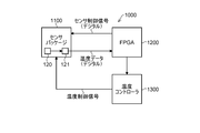
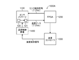
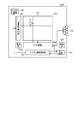
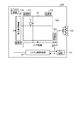
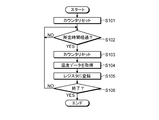
- thermometer circuit which concerns on 1st system configuration example of 1st Embodiment. It is a block diagram which shows the schematic configuration example of the imaging system which concerns on the 2nd system configuration example of 1st Embodiment. It is a layout diagram for demonstrating the arrangement of the thermometer circuit which concerns on 1st example of 1st Embodiment. It is a figure for demonstrating the arrangement of the thermometer circuit which concerns on 2nd example of 1st Embodiment. It is a figure for demonstrating the arrangement of the thermometer circuit which concerns on 3rd example of 1st Embodiment. It is a circuit diagram which shows an example of the thermometer circuit which concerns on 1st Embodiment.
- SWIR shortwave infrared
- the CMOS image sensor uses a photoelectric conversion unit provided on a silicon substrate as a light receiving element, and its sensitivity wavelength is physically up to about 1100 nm (nanometers), but a compound such as InGaAs is used as a photoelectric conversion film. By using it, it is possible to create an image sensor having sensitivity to infrared light having a wavelength of 1200 nm or more.
- photoelectric conversion materials with a smaller bandgap energy than silicon have higher sensitivity to temperature fluctuations than silicon. Therefore, the higher the temperature, the more noise called dark current is generated.
- an image sensor is used as a mechanism for cooling a chip containing a photoelectric conversion film (hereinafter, also referred to as a sensor chip) or keeping it at a constant temperature (hereinafter, also referred to as a temperature control mechanism). It may be installed in the package to be accommodated.
- a Perche element for example, a Perche element or the like can be used.
- a discrete thermistor element for measuring the temperature of the chip is attached to the sensor chip, and a temperature control circuit arranged outside the sensor chip controls the Pelche element based on the current or voltage output from the thermistor element. Can be considered.
- Temperature control can be executed by applying current or voltage to the Pelche element inside the package from, for example, a temperature control circuit outside the package through an external terminal provided in the package.
- the voltage or current that correlates with the temperature output from the thermistor element in the package is input to the temperature control circuit through the external terminal of the package.
- the purpose of temperature control is temperature-induced noise generated in the sensor chip, but in a configuration in which discrete thermistor elements are physically mounted in a package, the temperature of the sensor chip is not always accurately monitored. I can't. Since the thermal resistance from the sensor chip to the thermistor element varies depending on the mounting situation, the error of the signal output from the thermistor element is also large.
- the thermistor element is generally an analog output, it has low robustness against external noise. It is necessary to wire the output of the thermistor element to an external temperature control circuit, but since the control signal line and the power supply wiring are wired in parallel with this wiring, it is easy to have a capacity.
- a Perche element when, for example, a Perche element is used as the temperature control mechanism, it is necessary to dissipate the heat generated by this Perche element to the outside of the package. Therefore, a wide area where terminals are not provided is formed on the back surface of the package, and as a result, the number of terminals provided in the package cannot be increased.
- a terminal for outputting the output of the thermistor element to the outside of the package and a terminal for inputting the control signal of the Pelche element to the inside of the package are required. , Squeeze the number of terminals in the package.
- the addition of the thermistor element in the package contributes to the deterioration of the yield of the product as an image sensor due to the defect of the thermistor element itself and the mounting defect thereof.
- FIG. 1 is a block diagram showing a schematic configuration example of the solid-state image sensor according to the first embodiment.
- FIG. 2 is a circuit diagram showing a schematic configuration example of sensor pixels according to the first embodiment.
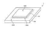
- FIG. 3 is a perspective view showing a schematic configuration example of the solid-state image sensor according to the first embodiment.
- the solid-state image sensor 1 is, for example, an infrared image sensor, and has sensitivity to, for example, light having a wavelength of 1200 nm or more.
- the solid-state image sensor 1 includes a pixel array unit 10 in which a plurality of sensor pixels 11 including a photoelectric conversion element are two-dimensionally arranged in a matrix shape.
- the sensor pixel 11 is composed of, for example, a pixel circuit 14 that performs photoelectric conversion and a readout circuit 15 that outputs a pixel signal based on the charge output from the pixel circuit 14.
- the pixel circuit 14 has, for example, a photodiode PD, a transfer transistor TRG, a floating diffusion FD, and an emission transistor OFG.
- the transfer transistor TRG and the emission transistor OFG are, for example, NMOS (Metal Oxide Semiconductor) transistors.
- the photodiode PD corresponds to a specific example of the "photoelectric conversion unit" of the present disclosure.
- the photodiode PD is a photoelectric conversion unit that absorbs light having a predetermined wavelength (for example, light having a wavelength in the infrared region of 1200 nm or more) to generate a signal charge.
- a photoelectric conversion material constituting the photodiode PD for example, a material containing a compound semiconductor such as a group III-V semiconductor can be used.
- III-V semiconductor used for the photodiode PD examples include InGaP, InAlP, InGaAs, InAlAs, and compound semiconductors having a chalcopyrite structure.
- a compound semiconductor having a chalcopyrite structure is a material that can obtain a high light absorption coefficient and high sensitivity over a wide wavelength range, and is preferably used as an n-type semiconductor material for photoelectric conversion.
- the photodiode PD may include amorphous silicon (Si), germanium (Ge), a quantum dot photoelectric conversion film, an organic photoelectric conversion film, and the like. In the following description, the case where InGaAs is used for the photodiode PD will be illustrated.
- the cathode of the photodiode PD is connected to the source of the transfer transistor TRG, and the anode of the photodiode PD is connected to the power supply line to which the voltage Vtop is applied.
- the drain of the transfer transistor TRG is connected to the floating diffusion FD, and the gate of the transfer transistor TRG is connected to the pixel drive line 12.
- the transfer transistor TRG is connected between the cathode of the photodiode PD and the floating diffusion FD, and transfers the electric charge held in the photodiode PD to the floating diffusion FD according to the control signal applied to the gate electrode. To do.
- the drain of the transfer transistor TRG is electrically connected to the floating diffusion FD, and the gate of the transfer transistor TRG is connected to the pixel drive line 12.
- the floating diffusion FD is a floating diffusion region that temporarily holds the electric charge transferred from the photodiode PD via the transfer transistor TRG.
- the reading circuit 15 is connected to the floating diffusion FD, and the vertical signal line 13 is connected via the reading circuit 15.
- the floating diffusion FD is connected to the input end of the read circuit 15.
- the drain is connected to the power supply line to which the voltage Vdr is applied, and the source is connected to the cathode of the photodiode PD.
- the emission transistor OFG initializes (reset) the charge of the photodiode PD according to the control signal applied to the gate electrode.
- the read-out circuit 15 has, for example, a reset transistor RST, a selection transistor SEL, and an amplification transistor AMP.
- the source of the reset transistor RST (the input end of the read circuit 15) is connected to the floating diffusion FD, and the drain of the reset transistor RST is connected to the power supply line VDD and the drain of the amplification transistor AMP.
- the gate of the reset transistor RST is connected to the pixel drive line 12.
- the source of the amplification transistor AMP is connected to the drain of the selection transistor SEL, and the gate of the amplification transistor AMP is connected to the source of the reset transistor RST.
- the source of the selection transistor SEL (the output end of the readout circuit 15) is connected to the vertical signal line 13, and the gate of the selection transistor SEL is connected to the pixel drive line 12.
- the reset transistor RST initializes (reset) the potential of the floating diffusion FD to a predetermined potential.
- the selection transistor SEL controls the output timing of the pixel signal from the readout circuit 15.
- the amplification transistor AMP generates a signal of a voltage corresponding to the level of the electric charge held in the floating diffusion FD as a pixel signal. That is, the amplification transistor AMP generates a signal having a voltage corresponding to the amount of light received by the sensor pixel 11 as a pixel signal.
- the amplification transistor AMP constitutes a source follower type amplifier, and outputs a pixel signal having a voltage corresponding to the level of electric charge generated by the photodiode PD.
- the selection transistor SEL When the selection transistor SEL is turned on, the amplification transistor AMP amplifies the potential of the floating diffusion FD and outputs a voltage corresponding to the potential to the horizontal selection circuit 40 described later via the vertical signal line 13.
- the selection transistor SEL may be provided between the power supply line VDD and the amplification transistor AMP.
- the drain of the reset transistor RST is connected to the drain of the power supply line VDD and the selection transistor SEL.
- the source of the selection transistor SEL is connected to the drain of the amplification transistor AMP, and the gate of the selection transistor SEL is connected to the pixel drive line 12.
- the source of the amplification transistor AMP (the output end of the readout circuit 15) is connected to the vertical signal line 13, and the gate of the amplification transistor AMP is connected to the source of the reset transistor RST.
- the solid-state image sensor 1 includes, for example, two substrates (light receiving substrate 100 and circuit board 200) as shown in FIG.
- the solid-state image sensor 1 has a three-dimensional structure (also referred to as a laminated structure) formed by laminating two substrates (light receiving substrate 100 and circuit board 200).
- the light receiving substrate 100 has a structure in which a plurality of photodiode PDs are formed in a matrix on an InGaAs substrate.
- the upper surface of the light receiving substrate 100 (the surface opposite to the circuit board 200) is the light receiving surface 100A.
- the circuit board 200 includes, for example, a structure in which a pixel signal generation circuit area 200A and a peripheral circuit area 200B are provided on one surface side of a silicon (Si) substrate.
- a plurality of pixel signal generation circuits 45 are formed in a matrix in the pixel signal generation circuit area 200A.
- Each pixel signal generation circuit 45 is a circuit of the sensor pixels 11 excluding the photodiode PD.
- the light receiving board 100 is joined to the pixel signal generation circuit area 200A in the circuit board 200.
- a circuit element such as a transistor is basically not built in the light receiving substrate 100, and it mainly functions as a photoelectric conversion film.
- the light emitted from the circuit element is also photoelectrically converted, so that a pixel circuit is formed below the light receiving substrate 100. This is because if a circuit element other than 14 (excluding the photodiode PD) is present, the light emitted from this circuit element may impair the uniformity of the pixels.
- a logic circuit for processing a pixel signal is formed in the peripheral circuit area 200B.
- a vertical drive circuit 20, a horizontal drive circuit 30, a horizontal selection circuit 40, a system control circuit 16, a film voltage control unit 17, and a voltage generation are formed.
- the circuit 18 is arranged.
- the logic circuit composed of these outputs a pixel signal (digital value) for each sensor pixel 11 to the outside.
- the peripheral circuit area 200B that is not covered by the light receiving substrate 100 may be covered with an insulating film such as a passivation, for example.
- the solid-state imaging device 1 includes a pixel array unit 10, a vertical drive circuit 20, a horizontal drive circuit 30, a horizontal selection circuit 40, a system control circuit 16, a film voltage control unit 17, and a voltage generation circuit 18.
- the system control circuit 16 Based on the master clock, the system control circuit 16 generates a clock signal, a control signal, and the like that serve as a reference for the operation of the vertical drive circuit 20, the horizontal drive circuit 30, the horizontal selection circuit 40, the membrane voltage control unit 17, and the like, and is vertical. It is given to the drive circuit 20, the horizontal selection circuit 40, the film voltage control unit 17, and the like.
- the vertical drive circuit 20 includes, for example, a shift register and controls row scanning of a plurality of sensor pixels 11 via a plurality of pixel drive lines 12.
- the horizontal selection circuit 40 is, for example, a circuit in which an ADC (Analog-to-Digital Converter) 40a and a switch element 40b are provided for each pixel row (or vertical signal line 13) of the pixel array unit 10.
- the ADC 40a AD-converts the pixel signal.
- the ADC 40a can change the analog range R, and sets the analog range R based on the range setting value input from the outside. In this embodiment, it is assumed that the analog range R is set to Ra.
- a vertical signal line 13 is connected to the input end of the ADC 40a, and a switch element 40b is connected to the output end of the ADC 40a.
- the horizontal drive circuit 30 is composed of, for example, a shift register or the like, and drives each switch element 40b of the horizontal selection circuit 40 in order. By driving each switch element 40b in order by the horizontal drive circuit 30, each pixel signal transmitted through each of the vertical signal lines 13 is sequentially output to the horizontal signal line 40c and input to the DSP circuit or the like.
- the membrane voltage control unit 17 controls the membrane voltage Vf applied to each photodiode PD based on the pixel signal obtained from the sensor pixel 11.
- the membrane voltage control unit 17 outputs a control signal for controlling the membrane voltage Vf to the voltage generation circuit 18.
- the voltage generation circuit 18 generates analog voltages (voltages Vtop and Vdr) based on the control signal input from the membrane voltage control unit 17, and applies them to each photodiode PD via the power supply line. That is, the film voltage control unit 17 and the voltage generation circuit 18 control the image quality of the image data obtained from the pixel signal by applying the film voltage Vf based on the pixel signal obtained from the sensor pixel 11 to each photodiode PD. ..
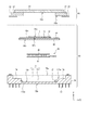
- FIG. 4 is a cross-sectional view showing a cross-sectional configuration example around the photoelectric conversion unit (photodiode PD) in the solid-state image sensor according to the first embodiment.
- the light receiving substrate 100 has an n-type semiconductor film 21 which is a photoelectric conversion unit (photodiode PD).
- the n-type semiconductor film 21 is formed on the entire surface of the pixel array portion 10, and is made of, for example, the material described above as a material used for the photodiode PD.
- the n-type semiconductor film 21 is made of InGaAs, and other configurations will be described.
- the light receiving substrate 100 further has a p-type semiconductor layer 22 in contact with the surface of the n-type semiconductor film 21 on the circuit board 200 side for each sensor pixel 11.
- Each p-type semiconductor layer 22 is formed of a high-concentration p-type semiconductor, for example, of p-type InGaAs.
- the p-type semiconductor layer 22 has a function as an electrode (second electrode) of the photodiode PD.
- a predetermined voltage Vdr is applied to the p-type semiconductor layer 22 via the discharge transistor OFG in the on state, or the voltage Vdd of the power supply line VDD is applied to the p-type semiconductor layer 22 via the transfer transistor TRG in the on state and the reset transistor RST. ..
- the light receiving substrate 100 further has an n-type semiconductor layer 23 that separates the p-type semiconductor layers 22 from each other.
- the n-type semiconductor layer 23 is formed in the same layer as each p-type semiconductor layer 22, and is formed by, for example, n-type InP.
- the light receiving substrate 100 further has an n-type semiconductor layer 24 in contact with the surface of the n-type semiconductor film 21 on the light receiving surface 100A side.
- the n-type semiconductor layer 24 is formed of an n-type semiconductor having a higher concentration than that of the n-type semiconductor film 21, and is formed of, for example, n-type InGaAs, n-type InP, or n-type InAlAs.
- the n-type semiconductor layer 24 functions as a barrier layer for preventing backflow of electric charges generated by the n-type semiconductor film 21.
- the light receiving substrate 100 further has an antireflection film 25 in contact with the surface of the n-type semiconductor layer 24 on the light receiving surface 100A side.
- the antireflection film 25 includes, for example, silicon nitride (SiN), hafnium oxide (HfO 2 ), aluminum oxide (Al 2 O 3 ), zirconium oxide (ZrO 2 ), tantalum oxide (Ta 2 Ta 5 ), and titanium oxide (Tio). It is formed by 2 ) and the like.
- the n-type semiconductor layer 24 also functions as an upper electrode (first electrode) of the electrodes that sandwich the n-type semiconductor film 21 vertically. A predetermined voltage Vtop is applied to the upper electrode.
- the light receiving substrate 100 further has a color filter 26 and an on-chip lens 27 on the antireflection film 25.
- the color filter 26 is composed of a plurality of filters 26R that selectively transmit red light, a plurality of filters 26G that selectively transmit green light, and a plurality of filters 26G that selectively transmit blue light.
- the plurality of filters 26R, 26G, and 26B are provided one by one for each sensor pixel 11, and are arranged in a Bayer array in a plane parallel to the light receiving surface 100A, for example.
- the sensor pixel 11 provided with the filter 26R is described as 11R
- the sensor pixel 11 provided with the filter 26G is described as 11G
- the sensor pixel 11 provided with the filter 26B is described as 11G. Is written as 11B.
- the color filter 26 may be omitted if necessary.
- the light receiving substrate 100 further has a passivation layer 28 and an insulating layer 29 under the p-type semiconductor layer 22 and the n-type semiconductor layer 23.
- the light receiving substrate 100 further has a connection electrode 31 that penetrates the passivation layer 28 and is in contact with the p-type semiconductor layer 22, and a bump electrode 32 that penetrates the insulation layer 29 and is in contact with the connection electrode 31.
- a set of connection electrodes 31 and bump electrodes 32 is provided for each sensor pixel 11.
- the bump electrode 32 is bonded to the connection layer 43 (described later) of the circuit board 200, and is electrically connected to the connection layer 43.
- the bump electrode 32 is joined to the connection layer 43 of the circuit board 200, for example, when the light receiving substrate 100 and the circuit board 200 are bonded to each other.
- the passivation layer 28 and the insulating layer 29 may be configured as an interlayer insulating layer. At that time, at least one of the passivation layer 28 and the insulating layer 29 may have a multilayer structure.
- the connection electrode 31 and the bump electrode 32 may be a part of the wiring provided in the layer-viewing insulating layer. In that case, the wiring of the interlayer insulating layer (bump electrode 32) and the wiring of the interlayer insulating layer 42 in the circuit board 200 (connection layer 43) are directly bonded to the light receiving substrate 100 (for example, the photodiode PD).
- a circuit board 200 (for example, a pixel circuit 14 other than the photodiode PD and a readout circuit 15) is electrically connected.
- the circuit board 200 includes a support board 41 and an interlayer insulating layer 42.
- the support substrate 41 is made of, for example, a silicon (Si) substrate.
- the interlayer insulating layer 42 is provided between the supporting substrate 41 and the insulating layer 291 (light receiving substrate 100).
- the interlayer insulating layer 42 is provided with, for example, a plurality of connection layers 43, a plurality of readout electrodes 44, a plurality of pixel signal generation circuits 45, and a plurality of wirings 46 in order from a position closest to the light receiving substrate 100.
- a plurality of sets of connection layers 43, a read electrode 44, a pixel signal generation circuit 45, and a wiring 46 are provided for each sensor pixel 11.
- a plurality of interlayer insulating layers 42 in the interlayer insulating layer 42 are provided in, for example, a ROIC (Read Out IC) for reading charges from each photodiode PD.
- the above-mentioned logic circuit is provided in a portion of the interlayer insulating layer 42 of the circuit board 200 corresponding to the peripheral circuit region 200B.
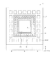
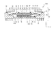
- FIGS. 5 and 6 are diagrams showing a configuration example of the solid-state image sensor according to the first embodiment.
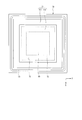
- FIG. 5 shows the planar configuration of the solid-state image sensor 1
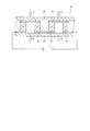
- FIG. 6 shows the cross-sectional configuration along the line AA of FIG.
- the solid-state image sensor 1 is provided with, for example, a plurality of light receiving unit regions P (sensor pixels 11) arranged two-dimensionally (FIG. 6).
- the solid-state image sensor 1 has an element region R1 in the central portion and a peripheral region R2 provided outside the element region R1 and surrounding the element region R1 (FIG. 5).
- the solid-state image sensor 1 has a conductive film 33 provided from the element region R1 to the peripheral region R2.
- the conductive film 33 has an opening in a region facing the central portion of the element region R1.
- the solid-state image sensor 1 has a laminated structure of a light receiving substrate 100 and a circuit board 200 (FIG. 6).
- One surface of the light receiving substrate 100 is a light incident surface (light incident surface S1), and the surface opposite to the light incident surface S1 (the other surface) is a bonding surface (joining surface S2) with the circuit board 200.
- the light receiving substrate 100 has an insulating layer 29, a connection electrode 31, a semiconductor layer 21A, an n-type semiconductor layer 24, and an antireflection film 25 in this order from a position close to the circuit board 200.
- the facing surface and the end surface (side surface) of the semiconductor layer 21A with the insulating layer 29 are covered with the passivation layer 28.
- the circuit board 200 is a so-called ROIC (Readout integrated circuit), and the light receiving board 100 is sandwiched between the wiring layer 35 and the interlayer insulating layer 42 in contact with the junction surface S2 of the light receiving board 100 and the wiring layer 35 and the interlayer insulating layer 42. It has a support substrate 41 facing the same.
- the light receiving substrate 100 has a semiconductor layer 21A in the element region R1.
- the region provided with the semiconductor layer 21A is the element region R1 of the solid-state image sensor 1.
- the region exposed from the conductive film 33 is the light receiving region.
- the region covered with the conductive film 33 is the OPB (Optical Black) region R1B.
- the OPB region R1B is provided so as to surround the light receiving region.
- the OPB region R1B is used to obtain a black level pixel signal.
- the light receiving substrate 100 has an embedded layer 36 together with a passivation layer 28 in the peripheral region R2.
- the peripheral region R2 is provided with holes H1 and H2 that penetrate the light receiving substrate 100 and reach the circuit board 200.
- the solid-state imaging device 1 light is incident on the semiconductor layer 21A from the light incident surface S1 of the light receiving substrate 100 via the antireflection film 25, the n-type semiconductor layer 24, and the n-type semiconductor layer 24.
- the signal charge photoelectrically converted by the semiconductor layer 21A moves through the connection electrode 31 and the insulating layer 29 and is read out by the circuit board 200.
- the configuration of each part will be described.
- the insulating layer 29 is provided over the element region R1 and the peripheral region R2, and has a bonding surface S2 with the circuit board 200.
- the joint surface S2 of the light receiving substrate 100 is provided in the element region R1 and the peripheral region R2.
- the joint surface S2 of the element region R1 and the joint surface S2 of the peripheral region R2 form the same plane. ing.
- the joint surface S2 of the peripheral region R2 is formed by providing the embedded layer 36.
- the insulating layer 29 has a bump electrode 32 and a dummy electrode 32D in, for example, the interlayer insulating films 29A and 29B constituting the insulating layer 29.
- an interlayer insulating film 29B is arranged on the circuit board 200 side, and an interlayer insulating film 29A is arranged on the p-type semiconductor layer 22 side, and these interlayer insulating films 29A and 29B are laminated and provided.
- the interlayer insulating films 29A and 29B are made of, for example, an inorganic insulating material.
- this inorganic insulating material examples include silicon nitride (SiN), aluminum oxide (Al 2 O 3 ), silicon oxide (SiO 2 ) and hafnium oxide (HfO 2 ).
- the interlayer insulating films 29A and 29B may be made of the same inorganic insulating material.
- the bump electrode 32 is provided in, for example, the element region R1.
- the bump electrode 32 is for electrically connecting the connection electrode 31 and the circuit board 200, and is provided in the element region R1 for each pixel P.
- the adjacent bump electrodes 32 are electrically separated by the embedded layer 36 and the interlayer insulating films 29A and 29B.
- the bump electrode 32 is composed of, for example, a copper (Cu) pad and is exposed on the joint surface S2.
- the dummy electrode 32D is provided in, for example, the peripheral region R2.
- the dummy electrode 32D is connected to the dummy connection layer 43D of the wiring layer 35 described later. By providing the dummy electrode 32D and the dummy connection layer 43D, it is possible to improve the strength of the peripheral region R2.
- the dummy electrode 32D is formed in the same process as the bump electrode 32, for example.
- the dummy electrode 32D is composed of, for example, a copper (Cu) pad and is exposed on the joint surface S2.
- connection electrode 31 provided between the bump electrode 32 and the semiconductor layer 21A has a signal charge generated in the n-type semiconductor film 21 (holes or electrons, hereinafter for convenience, the signal charge will be described as a hole). It is an electrode (anode) to which a voltage for reading is supplied, and is provided for each pixel P in the element region R1.
- the connection electrode 31 is provided so as to embed the opening of the passivation layer 28, and is in contact with the semiconductor layer 21A (more specifically, the diffusion region 22A).
- the connection electrode 31 is larger than the opening of the passivation layer 28, for example, and a part of the connection electrode 31 is provided in the embedded layer 36.
- connection electrode 31 (the surface on the semiconductor layer 21A side) is in contact with the diffusion region 22A, and the lower surface and a part of the side surface of the connection electrode 31 are in contact with the embedded layer 36.
- the adjacent connection electrodes 31 are electrically separated by a passivation layer 28 and an embedded layer 36.
- connection electrode 31 is, for example, titanium (Ti), tungsten (W), titanium nitride (TiN), platinum (Pt), gold (Au), germanium (Ge), palladium (Pd), zinc (Zn), nickel ( It is composed of a single substance of Ni) and aluminum (Al), or an alloy containing at least one of them.
- the connection electrode 31 may be a single film of such a constituent material, or may be a laminated film in which two or more kinds are combined.
- the connection electrode 31 is made of a laminated film of titanium and tungsten.
- the thickness of the connection electrode 31 is, for example, several tens of nm to several hundreds of nm.
- the semiconductor layer 21A includes, for example, a p-type semiconductor layer 22, an n-type semiconductor film 21, and an n-type semiconductor layer 24 from a position close to the insulating layer 29.
- the p-type semiconductor layer 22, the n-type semiconductor film 21, and the n-type semiconductor layer 24 have the same planar shape, and their end faces are arranged at the same positions in a plan view.
- the p-type semiconductor layer 22 is provided in common to all pixels P, for example, and is arranged between the passivation layer 28 and the n-type semiconductor film 21.
- the p-type semiconductor layer 22 is for electrically separating adjacent pixels P, and the p-type semiconductor layer 22 is provided with, for example, a plurality of diffusion regions 22A.
- a compound semiconductor material having a bandgap larger than the bandgap of the compound semiconductor material constituting the n-type semiconductor film 21 for the p-type semiconductor layer 22 dark current can be suppressed.
- n-type InP indium phosphide
- the diffusion regions 22A provided in the p-type semiconductor layer 22 are arranged apart from each other.
- the diffusion region 22A is arranged for each pixel P, and the connection electrode 31 is connected to each diffusion region 22A.
- a diffusion region 22A is also provided in the OPB region R1B.
- the diffusion region 22A is for reading out the signal charge generated in the n-type semiconductor film 21 for each pixel P, and contains, for example, a p-type impurity. Examples of the p-type impurity include Zn (zinc) and the like. In this way, a pn junction interface is formed between the diffusion region 22A and the p-type semiconductor layer 22 other than the diffusion region 22A, and adjacent pixels P are electrically separated.
- the diffusion region 22A is provided, for example, in the thickness direction of the p-type semiconductor layer 22, and is also provided in a part of the n-type semiconductor film 21 in the thickness direction.
- the n-type semiconductor film 21 between the connection electrode 31 and the n-type semiconductor layer 24, more specifically, between the p-type semiconductor layer 22 and the n-type semiconductor layer 24, is common to all pixels P, for example. It is provided.
- the n-type semiconductor film 21 absorbs light having a predetermined wavelength to generate a signal charge, and is made of, for example, a compound semiconductor material such as an i-type III-V group semiconductor.
- Examples of the compound semiconductor material constituting the n-type semiconductor film 21 include InGaAs (indium gallium arsenide), InAsSb (indium arsenide antimony), InAs (indium arsenide), InSb (indium antimony) and HgCdTe (mercury cadmium tellurium). Can be mentioned.
- the n-type semiconductor film 21 may be formed of Ge (germanium). In the n-type semiconductor film 21, for example, photoelectric conversion of light having a wavelength in the visible region to the short infrared region is performed.
- the n-type semiconductor layer 24 is provided in common to all pixels P, for example.
- the n-type semiconductor layer 24 is provided between the n-type semiconductor film 21 and the n-type semiconductor layer 24 and is in contact with the n-type semiconductor layer 24.
- the n-type semiconductor layer 24 is a region in which charges discharged from the n-type semiconductor layer 24 move, and is composed of, for example, a compound semiconductor containing n-type impurities.
- n-type InP indium phosphide
- the n-type semiconductor layer 24 is provided, for example, as an electrode common to each pixel P, on the n-type semiconductor layer 24 (on the light incident side) so as to be in contact with the n-type semiconductor layer 24.
- the n-type semiconductor layer 24 is for discharging a charge that is not used as a signal charge among the charges generated by the n-type semiconductor film 21 (cathode). For example, when holes are read out from the connection electrode 31 as signal charges, electrons can be discharged, for example, through the n-type semiconductor layer 24.
- the n-type semiconductor layer 24 is made of a conductive film capable of transmitting incident light such as infrared rays.
- n-type semiconductor layer 24 for example, ITO (Indium Tin Oxide) or ITOO (In 2 O 3- TIO 2 ) or the like can be used.
- the n-type semiconductor layer 24 may be provided in a grid pattern so as to partition adjacent pixels P, for example.
- a conductive material having low light transmittance can be used for the n-type semiconductor layer 24.
- the antireflection film 25 covers the n-type semiconductor layer 24 from the light incident surface S1 side.
- the antireflection film 25 may have an antireflection function.
- silicon nitride (SiN), aluminum oxide (Al 2 O 3 ), silicon oxide (SiO 2 ), tantalum oxide (Ta 2 O 3 ) and the like can be used.
- the antireflection film 25 has an opening 37H in the OPB region R1B.
- the opening 37H is provided, for example, in a frame shape surrounding the light receiving region (FIG. 5).
- the opening 37H may be, for example, a quadrangular or circular hole in a plan view.
- the conductive film 33 is electrically connected to the n-type semiconductor layer 24 by the opening 37H of the antireflection film 25.
- the passion layer 28 is provided between the p-type semiconductor layer 22 and the embedded layer 36, and is the end face of the p-type semiconductor layer 22, the end face of the n-type semiconductor film 21, the end face of the n-type semiconductor layer 24, and the n-type semiconductor. It covers the end face of the layer 24 and is in contact with the antireflection film 25 in the peripheral region R2.
- the passivation layer 28 is composed of, for example, an oxide such as silicon oxide (SiO X ) or aluminum oxide (Al 2 O 3 ).
- the passivation layer 28 may be formed by a laminated structure composed of a plurality of films.
- the passivation layer 28 may be made of a silicon (Si) -based insulating material such as silicon oxynitride (SiON), carbon-containing silicon oxide (SiOC), silicon nitride (SiN), and silicon carbide (SiC).
- Si silicon oxynitride
- SiOC carbon-containing silicon oxide
- SiN silicon nitride
- SiC silicon carbide
- the thickness of the passivation layer 28 is, for example, several tens of nm to several hundreds of nm.
- the conductive film 33 is provided from the OPB region R1B to the hole H1 in the peripheral region R2.
- the conductive film 33 is in contact with the n-type semiconductor layer 24 at the opening 37H of the antireflection film 25 provided in the OPB region R1B, and is in contact with the wiring 46 of the circuit board 200 through the hole H1.
- a voltage is supplied from the circuit board 200 to the n-type semiconductor layer 24 via the conductive film 33.
- the conductive film 33 functions as a voltage supply path to the n-type semiconductor layer 24 and also as a light-shielding film, and forms the OPB region R1B.
- the conductive film 33 is made of a metal material containing, for example, tungsten (W), aluminum (Al), titanium (Ti), molybdenum (Mo), tantalum (Ta) or copper (Cu).
- a passivation film may be provided on the conductive film 33.
- An adhesive layer B may be provided between the end of the n-type semiconductor layer 24 and the n-type semiconductor layer 24. As will be described later, this adhesive layer B is used when forming the solid-state image sensor 1, and plays a role of joining the semiconductor layer 21A to a temporary substrate (not shown).
- the adhesive layer B is made of, for example, tetraethoxysilane (TEOS) or silicon oxide (SiO 2 ).
- TEOS tetraethoxysilane
- SiO 2 silicon oxide
- the adhesive layer B is provided, for example, wider than the end face of the p-type semiconductor layer 22, and is covered with the embedded layer 36 together with the semiconductor layer 21A.
- a passivation layer 28 is provided between the adhesive layer B and the embedded layer 36.
- the adhesive layer B may be provided over a wide region of the peripheral region R2.
- the adhesive layer B extends from the vicinity of the edge of the semiconductor layer 21A (element region R1) to between the holes H1 and H2. May be good.
- the adhesive layer B may extend from the vicinity of the edge of the semiconductor layer 21A (element region R1) to the chip end (chip end E).
- the embedded layer 36 is for filling a step between the temporary substrate and the semiconductor layer 21A in the manufacturing process of the solid-state image sensor 1. Although the details will be described later, in the present embodiment, since the embedded layer 36 is formed, it is possible to suppress the occurrence of defects in the manufacturing process due to the step between the semiconductor layer 21A and the temporary substrate.
- the embedded layer 36 of the peripheral region R2 is provided between the insulating layer 29 and the passivation layer 28, and between the insulating layer 29 and the antireflection film 25, and has, for example, a thickness equal to or greater than the thickness of the semiconductor layer 21A. ing.
- the embedded layer 36 is provided so as to surround the semiconductor layer 21A, a region around the semiconductor layer 21A (peripheral region R2) is formed.
- the joint surface S2 with the circuit board 200 can be provided in the peripheral region R2. If the joint surface S2 is formed in the peripheral region R2, the thickness of the embedded layer 36 may be reduced, but the embedded layer 36 covers the semiconductor layer 21A in the thickness direction, and the entire end surface of the semiconductor layer 21A is buried.
- the embedded layer 36 can effectively suppress the infiltration of water into the semiconductor layer 21A.
- the embedded layer 36 of the element region R1 is provided between the semiconductor layer 21A and the insulating layer 29 so as to cover the connection electrode 31.
- the surface of the embedded layer 36 on the joint surface S2 side is flattened, and in the peripheral region R2, the insulating layer 29 is provided on the surface of the flattened embedded layer 36.
- an inorganic insulating material such as silicon oxide (SiO X), silicon nitride (SiN), silicon oxynitride (SiON), carbon-containing silicon oxide (SiOC), and silicon carbide (SiC) is used. Can be done.
- the insulating layer 29 including the interlayer insulating films 29A and 29B and the bump electrode 32 is formed above the embedded layer 36. Will be done.
- a circuit board 200 including a wiring layer 35 is attached to a light receiving substrate 100 including the insulating layer 29 to form a solid-state image sensor 1.
- the bump electrode 32 of the insulating layer 29 and the connecting layer 43 of the wiring layer 35 are connected.
- the bump electrode 32 and the connecting layer 43 have, for example, a Cu pad, and the bump electrode 32 and the connecting layer 43 are connected by direct bonding of the Cu pad.
- the embedded layer 36 arranged below the copper film to be polished is required to have a hardness that can withstand the stress during polishing. Further, in order to directly bond the Cu pads of the bump electrode 32 and the connection layer 43 to each other, it is necessary to form the light receiving substrate 100 and the circuit board 200 extremely flat. Therefore, it is preferable that the embedded layer 36 arranged below the copper film has a hardness that can withstand the stress during polishing.
- the constituent material of the embedded layer 36 is preferably a material having a higher hardness than the encapsulant or the organic material arranged around the die in a general semiconductor package. Examples of the material having such high hardness include an inorganic insulating material.
- the embedded layer 36 can be formed by forming a film of this inorganic insulating material by, for example, a CVD (Chemical Vapor Deposition) method, a sputtering method, or a coating method.
- the embedded layer 36 is provided with holes H1 and H2 penetrating the embedded layer 36.
- the holes H1 and H2 penetrate the insulating layer 29 together with the embedded layer 36 and reach the circuit board 200.
- the holes H1 and H2 have, for example, a quadrangular planar shape, and a plurality of holes H1 and H2 are provided so as to surround the element region R1 (FIG. 5).
- the hole H1 is provided at a position closer to the element region R1 than the hole H2, and the side wall and the bottom surface of the hole H1 are covered with the conductive film 33.
- the hole H1 is for connecting the n-type semiconductor layer 24 (conductive film 33) and the wiring of the circuit board 200 (wiring 46 described later), and is an antireflection film 25, an embedded layer 36, and an insulating layer 29. It is provided through.
- the hole H2 is provided at a position closer to the tip end E than the hole H1, for example.
- the hole H2 penetrates the antireflection film 25, the embedding layer 36, and the insulating layer 29, and reaches the pad electrode (pad electrode 38 described later) of the circuit board 200.
- An electrical connection between the outside and the solid-state image sensor 1 is made through the hole H2.
- the holes H1 and H2 do not have to reach the circuit board 200.
- the holes H1 and H2 may reach the wiring of the insulating layer 29, and this wiring may be connected to the wiring 46 and the pad electrode 38 of the circuit board 200.
- the holes H1 and H2 may penetrate the adhesive layer B.
- the distance between the connection electrode 31 and the n-type semiconductor layer 24 is a distance sufficient for photoelectric conversion and not too far apart. That is, it is preferable to reduce the thickness of the light receiving substrate 100.
- the distance between the connection electrode 31 and the n-type semiconductor layer 24 or the thickness of the light receiving substrate 100 is 10 ⁇ m or less, further 7 ⁇ m or less, and further 5 ⁇ m or less.
- the support substrate 41 of the circuit board 200 faces the light receiving substrate 100 with the wiring layer 35 and the interlayer insulating layer 42 in between.
- the support substrate 41 is made of, for example, silicon (Si).
- a plurality of transistors are provided in the vicinity of the surface of the support substrate 41 (the surface on the wiring layer 35 side). For example, a read out circuit is configured for each pixel P by using the plurality of transistors.
- the wiring layer 35 has, for example, the interlayer insulating film 35A and the interlayer insulating film 35B in this order from the light receiving substrate 100 side, and these interlayer insulating films 35A and 35B are provided in a laminated manner.
- a connection layer 43 and a dummy connection layer 43D are provided in the interlayer insulating film 35A.
- the interlayer insulating layer 42 is provided so as to face the light receiving substrate 100 with the wiring layer 35 in between.
- a pad electrode 38 and a plurality of wirings 46 are provided in the interlayer insulating layer 42.
- the interlayer insulating films 35A and 35B are made of, for example, an inorganic insulating material. Examples of this inorganic insulating material include silicon nitride (SiN), aluminum oxide (Al 2 O 3 ), silicon oxide (SiO 2 ) and hafnium oxide (HfO 2 ).
- connection layer 43 is for electrically connecting the connection electrode 31 and the wiring 46, and is provided in the element region R1 for each pixel P.
- the connection layer 43 is in contact with the bump electrode 32 at the joint surface S2 of the light receiving substrate 100.
- the adjacent connecting layers 43 are electrically separated by the interlayer insulating film 35A.
- the dummy connection layer 43D provided in the peripheral region R2 is in contact with the dummy electrode 32D at the joint surface S2 of the light receiving substrate 100.
- the dummy connection layer 43D is formed, for example, in the same process as the connection layer 43.
- the connection layer 43 and the dummy connection layer 43D are composed of, for example, copper (Cu) pads, and are exposed on the surface of the circuit board 200 facing the light receiving board 100. That is, for example, CuCu bonding is performed between the bump electrode 32 and the connection layer 43, and between the dummy electrode 32D and the dummy connection layer 43D. Details will be described later, but this makes it possible to miniaturize the pixel P.
- the wiring 46 connected to the bump electrode 32 is connected to a transistor provided near the surface of the support substrate 41, and the connection electrode 31 and the read circuit are connected to each pixel P.
- the wiring 46 connected to the conductive film 33 via the hole H1 is connected to, for example, a predetermined potential.
- one of the electric charges (for example, holes) generated in the n-type semiconductor film 21 is read out from the connection electrode 31 to the reading circuit via the bump electrode 32 and the connection layer 43, and the n-type semiconductor film 21
- the other side (for example, electrons) of the electric charge generated in is discharged from the n-type semiconductor layer 24 to a predetermined potential via the conductive film 33.
- the pad electrode 38 provided in the peripheral region R2 is for making an electrical connection with the outside.
- a hole H2 that penetrates the light receiving substrate 100 and reaches the pad electrode 38 is provided in the vicinity of the chip end E of the solid-state image sensor 1, and is electrically connected to the outside through the hole H2. ..
- the connection is made, for example, by a method such as wire bonding or bumping.
- a predetermined potential may be supplied from the external terminal arranged in the hole H2 to the n-type semiconductor layer 24 via the wiring 46 of the hole H2 and the conductive film 33.
- the signal voltage read from the connection electrode 31 is read out to the read circuit of the support substrate 41 via the bump electrode 32 and the connection layer 43, and this read circuit is used. It may be output to an external terminal arranged in the hole H2 via the circuit. The signal voltage may be output to an external terminal together with the read circuit via, for example, another circuit included in the circuit board 200.
- Other circuits include, for example, signal processing circuits and output circuits.
- the thickness of the circuit board 200 is preferably larger than the thickness of the light receiving board 100.
- the thickness of the circuit board 200 is preferably 2 times or more, further 5 times or more, further 10 times or more larger than the thickness of the light receiving substrate 100.
- the thickness of the circuit board 200 is, for example, 100 ⁇ m or more, 150 ⁇ m or more, or 200 ⁇ m or more.
- the circuit board 200 having such a large thickness ensures the mechanical strength of the solid-state image sensor 1.
- the circuit board 200 may include only one layer of the support board 41 forming the circuit, or may further include a board such as a support board in addition to the support board 41 forming the circuit. Good.
- FIG. 7 is a cross-sectional view showing an example of the joining structure of the first embodiment.
- each sensor pixel 11 in the pixel array unit 10 is divided into a normal pixel 11a or a charge emission pixel 11b depending on the control of the reset transistor RST, but the pixel structure is a normal pixel 11a and a charge emission pixel. Since both of 11b are the same, it will be described simply as the sensor pixel 11.
- the charge emission pixel 11b is arranged on the outermost side of the pixel array unit 10.
- the transfer transistor TRG, emission transistor OFG, floating diffusion FD, reset transistor RST, amplification transistor AMP, and pixel signal generation circuit 45 of the selection transistor SEL of each sensor pixel 11 are made of a single crystal material such as single crystal silicon (Si). It is formed for each pixel on the circuit board 200 made of.
- the reference numerals of the transfer transistor TRG, the discharge transistor OFG, the floating diffusion FD, the reset transistor RST, the amplification transistor AMP, and the selection transistor SEL formed on the circuit board 200 are omitted.
- An n-type semiconductor film 21 serving as a photodiode PD is formed on the entire surface of the pixel array portion 10 on the upper side of the circuit board 200 on the light incident side.
- As the n-type semiconductor film 21, InGaP, InAlP, InGaAs, InAlAs, and further compound semiconductors having a chalcopyrite structure are used as the n-type semiconductor film 21, InGaP, InAlP, InGaAs, InAlAs, and further compound semiconductors having a chalcopyrite structure are used.
- a compound semiconductor having a chalcopyrite structure is a material that can obtain a high light absorption coefficient and high sensitivity over a wide wavelength range, and is preferably used as an n-type semiconductor film 21 for photoelectric conversion.
- Such a compound semiconductor having a chalcopyrite structure is composed of elements around Group IV elements such as Cu, Al, Ga, In, S, and Se, and is composed of CuGaInS-based mixed crystals, CuAlGaInS-based mixed crystals, and CuAlGaInSse-based. Examples include mixed crystals.
- amorphous silicon (Si), germanium (Ge), quantum dot photoelectric conversion film, organic photoelectric conversion film and the like can also be used.
- a high-concentration p-type semiconductor layer 22 constituting a pixel electrode is formed for each pixel on the lower side of the n-type semiconductor film 21 on the circuit board 200 side. Then, between the high-concentration p-type semiconductor layers 22 formed for each pixel, an n-type semiconductor layer 23 as a pixel separation region for separating each sensor pixel 11 is formed of, for example, a compound semiconductor such as InP. ing.
- the n-type semiconductor layer 23 has a role of preventing dark current as well as a function as a pixel separation region.
- an n-type semiconductor layer 24 having a higher concentration than that of the n-type semiconductor film 21 is formed by using a compound semiconductor such as InP used as a pixel separation region. ing.
- the high-concentration n-type semiconductor layer 24 functions as a barrier layer for preventing the backflow of electric charges generated by the n-type semiconductor film 21.
- compound semiconductors such as InGaAs, InP, and InAlAs can be used.
- An antireflection film 25 is formed on the high-concentration n-type semiconductor layer 24 as a barrier layer.
- the material of the antireflection film 25 includes, for example, silicon nitride (SiN), hafnium oxide (HfO 2 ), aluminum oxide (Al 2 O 3 ), zirconium oxide (ZrO 2 ), tantalum oxide (Ta 2 Ta 5 ), and oxidation. Titanium (TiO 2 ) or the like can be used.
- Either one of the high-concentration n-type semiconductor layer 24 or the antireflection film 25 also functions as an upper upper electrode among the electrodes sandwiching the n-type semiconductor film 21 above and below, and the high-concentration n-type as the upper electrode.
- a predetermined voltage Va is applied to the semiconductor layer 24 or the antireflection film 25.
- a color filter 26 and an on-chip lens 27 are further formed on the antireflection film 25.
- the color filter 26 is a filter that transmits light (wavelength light) of either R (red), G (green), or B (blue).
- the color filter 26 is arranged in a so-called Bayer array in the pixel array unit 10. ing.
- a passivation layer 28 and an insulating layer 29 are formed under the high-concentration p-type semiconductor layer 22 constituting the pixel electrode and the n-type semiconductor layer 23 as the pixel separation region.
- the connection electrode 31, the connection layer 43, and the bump electrode 32 are formed so as to penetrate the passivation layer 28 and the insulating layer 29.
- the connection electrode 31, the connection layer 43, and the bump electrode 32 electrically connect the high-concentration p-type semiconductor layer 22 constituting the pixel electrode and the floating diffusion FD that accumulates electric charges.
- the normal pixel 11a and the charge emission pixel 11b are configured as described above and have the same pixel structure.
- control method of the reset transistor RST is different between the normal pixel 11a and the charge emission pixel 11b.
- the reset transistor RST is turned on and off based on the reset signal RST according to the charge generation period (light receiving period) by the photodiode PD, the reset period of the potential of the floating diffusion FD before the start of light receiving, and the like.
- the reset transistor RST is always controlled to be ON. As a result, the electric charge generated by the photodiode PD is discharged to the ground, and a constant voltage Va is always applied to the electric charge emission pixel 11b.
- FIG. 8 is a plan view showing a configuration example of a sensor package (also referred to as an image pickup apparatus) according to the first embodiment.
- FIG. 9 is a cross-sectional view showing a configuration example of the sensor package according to the first embodiment. Note that FIG. 9 shows a cross section of FIG. 8 cut along the XX plane passing through the BB line.
- the sensor package 1100 includes a package 50 and a lid 60 with a sealing glass (an example of the lid) attached to the upper surface 50a side of the package 50.
- the package 50 includes a package substrate 70, a Perche element 80, a ceramic interposer substrate 90 (also referred to as a support substrate), and a solid-state image pickup device 1. First, the configuration of the package 50 will be described.
- FIG. 10 is an exploded cross-sectional view showing a configuration example of the sensor package according to the first embodiment.
- the package substrate 70 is a multilayer substrate made of ceramic such as alumina (aluminum oxide), and is, for example, a PGA (Pin Grid Array) substrate.
- the package substrate 70 has a first surface (for example, an upper surface 70a) and a second surface (for example, a lower surface 70b) located on the opposite side of the first surface.
- a plurality of wirings are provided in multiple layers inside the package substrate 70 located between the upper surface 70a and the lower surface 70b. These wirings are connected to a plurality of terminals (for example, pin-shaped terminals 73) provided on the lower surface 70b of the package substrate 70.
- FIG. 11 is a plan view showing a configuration example of the upper surface side of the package substrate according to the first embodiment.
- a cavity 71 is provided on the upper surface 70a side of the package substrate 70.
- the cavity 71 has a first recess 111 and a second recess 112 (an example of the recess) provided on the bottom surface 111a of the first recess 111.
- the shapes of the first recess 111 and the second recess 112 in a plan view are, for example, rectangular.
- the diameter of the opening surface of the first recess 111 is larger than that of the second recess 112.
- a perche element 80 as a temperature control element is arranged in the second recess 112, and for example, the perche element 80 is attached to the bottom surface 112a of the second recess 112 via an adhesive 51 (see FIG. 9). ..
- the upper surface of the Pelche element 80 arranged in the second recess 112 (for example, the upper surface 85a of the second ceramic substrate 85 described later) is at the same height as or substantially the same height as the bottom surface 111a of the first recess 111.
- a pin-shaped terminal 72 for connecting to the lead wire of the Pelche element 80 is provided on the bottom surface 112a of the second recess 112. Two pin-shaped terminals 72 are provided. Of the two pin-shaped terminals 72, one is connected to the lead wire of the positive electrode of the Perche element 80, and the other is connected to the lead wire of the negative electrode of the Perche element 80.
- the external connection terminal can be a ball terminal, a land terminal, or the like instead of the pin-shaped terminal 73.
- a seal ring 75 is provided on the upper surface 70a side of the outer peripheral portion of the package substrate 70.
- the seal ring 75 is continuously provided so as to surround the cavity 71 of the package substrate 70 in a plan view.
- the seal ring 75 is a portion to be joined to a metal portion 63 described later of the lid 60 with a seal glass.
- the seal ring 75 is, for example, an alloy of iron (Fe) -nickel (Ni) -cobalt (Co) (so-called Kovar), which has been surface-treated by plating Ni, gold (Au), or the like.
- FIG. 12 is a plan view illustrating the positional relationship between the package substrate and the ceramic interposer substrate according to the first embodiment.
- the lower surface 90b side of the ceramic interposer substrate 90 is attached to the bottom surface 111a of the first recess 111 and the Perche element 80 via an adhesive 51.
- the ceramic interposer substrate 90 is arranged so as to cover the entire opening surface of the second recess 112.
- a plurality of bonding pads 74 are provided on the bottom surface 111a of the first recess 111, which is exposed from below the ceramic interposer substrate 90. Further, a plurality of bonding pads 91 are provided on the lower surface 90b side of the ceramic interposer substrate 90. At least a part of the plurality of bonding pads 91 is connected to the bonding pad 74 via a wire 54. Further, at least a part of the plurality of bonding pads 91 is connected to the bonding pad 92 of the solid-state image sensor 1 via a wire 55. Alternatively, both the wires 54 and 55 may be connected to one bonding pad 91.
- the wires 54 and 55 are, for example, gold wires.
- a bonding pad 92 is provided in the outer peripheral region on the upper surface 93a side of the solid-state image sensor 1.
- the lower surface 93b side of the solid-state image sensor 1 is attached to the lower surface 90b side of the ceramic interposer substrate 90 via an adhesive 51.
- FIG. 13 is a cross-sectional view showing a configuration example of the Perche element according to the first embodiment.
- the Perche element 80 includes a first ceramic substrate 81, a first copper electrode 82 provided on the first ceramic substrate 81, a second ceramic substrate 85 facing the first ceramic substrate 81, and a second ceramic substrate 85. 2 It has a second copper electrode 86 provided on a ceramic substrate 85, a P-type thermoelectric semiconductor 87, and an N-type thermoelectric semiconductor 88.
- the P-type thermoelectric semiconductor 87 and the N-type thermoelectric semiconductor 88 are arranged between the first ceramic substrate 81 and the second ceramic substrate 85, respectively.
- Each of the P-type thermoelectric semiconductor 87 and the N-type thermoelectric semiconductor 88 has one end connected to the first copper electrode 82 and the other end connected to the second copper electrode 86.
- the P-type thermoelectric semiconductor 87 and the N-type thermoelectric semiconductor 88 are alternately connected in series via the first copper electrode 82 and the second copper electrode 86.
- the Perche element 80 when a direct current is passed from the N-type thermoelectric semiconductor 88, the second ceramic substrate 85 absorbs (endothermics) heat T1 and the first ceramic substrate 81 heats. Emit T2 (dissipate heat). Since the second ceramic substrate 85 is attached to the ceramic interposer substrate 90 via the adhesive 51 and the first ceramic substrate 81 is attached to the package substrate 70 via the adhesive 51, the Perche element 80 is a solid-state imaging device. The heat generated in the first magnitude can be released from the ceramic interposer substrate 90 to the package substrate 70.
- the lid 60 with a sealing glass is provided on the sealing glass 61, the ceramic frame 62 provided on the lower surface 61b side of the outer peripheral portion of the sealing glass 61, and the lower surface 62b side of the ceramic frame 62. It has a metal portion 63 and a metal portion 63.
- the seal glass 61 and the ceramic frame 62 are joined to each other by, for example, low melting point glass.
- the ceramic frame 62 and the metal portion 63 are joined to each other with, for example, Ag—Cu brazing material.
- the metal portion 63 is a portion to be joined to the seal ring 75 of the package substrate 70 by means such as seam welding.
- the metal portion 63 is made of the same material as the seal ring 75.
- it is an alloy of iron (Fe) -nickel (Ni) -cobalt (Co) (so-called Kovar), and Ni and gold (Au). ) Etc. are surface-treated by plating.
- the lid 60 with a sealing glass is joined to the upper surface 50a side of the package 50, and the upper surface 50a side of the package 50 is airtightly sealed.
- Temperature control mechanism In the solid-state image sensor 1 using a photoelectric conversion material having a smaller band gap energy than silicon, in other words, having sensitivity to light having a wavelength of about 1200 nm or more, as described above. As described above, in order to suppress the generation of dark current, which is noise, it is necessary to provide a mechanism (temperature control mechanism) for cooling the sensor chip or keeping it at a constant temperature.
- thermometer circuit is arranged in the solid-state imaging device 1, and the Perche element in the package can be controlled from the temperature control circuit arranged outside the package based on the output from the thermometer circuit. Configure. As a result, it is possible to obtain merits in terms of accuracy of the measured sensor chip temperature, robustness of the measured temperature, restrictions on the number of terminals, yield, and the like.
- thermometer circuit 120 as the temperature sensor according to the present embodiment is built in, for example, the circuit board 200 of the solid-state imaging device 1.
- the current or voltage which is the measurement result output from the thermometer circuit 120, is output to the outside of the sensor package 1100 via, for example, the bonding pad 91, the wire 54, the bonding pad 74, and the pin-shaped terminal 73.
- an AD conversion circuit 121 that converts an analog current or voltage value output from the thermometer circuit 120 into a digital value is provided in the circuit board 200, and is output from the AD conversion circuit 121.
- the digital value may be output to the outside of the sensor package 1100 via the pin-shaped terminal 73 or the like.
- the ADC 40a in the horizontal selection circuit 40 may be used for the AD conversion circuit 121, or a dedicated ADC built in the circuit board 200 separately from the ADC 40a may be used.
- thermometer circuit 120 is not limited to the circuit board 200, and may be provided on the light receiving board 100 side, for example.
- FIG. 14 is a block diagram showing a schematic configuration example of an imaging system according to the first system configuration example of the first embodiment.
- the imaging system 1000 according to the first system configuration example includes the above-mentioned sensor package 1100, FPGA (Field-Programmable Gate Array) 1200, and temperature controller 1300.
- FPGA Field-Programmable Gate Array
- the sensor package 1100 includes a structure for accommodating the solid-state image sensor 1 in the cavity 71 formed by the package 50 and the lid 60 with a sealing glass.
- the FPGA 1200 is, for example, a control device for controlling the solid-state image sensor 1, and inputs a control signal for controlling the solid-state image sensor 1 to the solid-state image sensor 1 inside the package 50 via a pin-shaped terminal.
- I2C Inter-Integrated Circuit
- SPI Serial Peripheral Interface
- An information processing device such as an ISP (Image Signal Processor) may be used instead of the FPGA 1200.
- the temperature data (detection result) detected by the thermometer circuit 120 of the solid-state image sensor 1 and converted into a digital value by the AD conversion circuit 121 is, for example, an interface such as I2C or SPI that connects the FPGA 1200 and the solid-state image sensor 1. It is output to the FPGA 1200 outside the package via the same interface as. Therefore, in the present embodiment, the dedicated line and the dedicated terminal for outputting the temperature data to the outside of the package can be omitted.
- the temperature controller 1300 is configured to control the perche element 80 in the sensor package 1100 according to, for example, a control signal from the FPGA 1200. Specifically, the temperature controller 1300 generates a current waveform to be applied to the Pelche element 80 according to a control signal from the FPGA 1200, and supplies this to the Pelche element 80 in the sensor package 1100 via the pin-shaped terminal 73.
- thermometer circuit 120 since the thermometer circuit 120 is arranged in the solid-state image sensor 1, it is possible to directly measure the temperature of the solid-state image sensor 1 itself. This makes it possible to improve the accuracy of the measured sensor chip temperature.
- thermometer circuit 120 since the analog value output from the thermometer circuit 120 is converted into a digital value by the AD conversion circuit 121 in the solid-state image sensor 1, the influence of noise of the measurement result detected by the thermometer circuit 120 is reduced. It becomes possible to do. Thereby, it becomes possible to enhance the robustness of the measurement temperature.
- the measurement result can be output to the outside of the sensor package 1100 using a control signal such as I2C or SPI, so that the measurement result is output to the outside of the sensor package 1100.
- a control signal such as I2C or SPI
- the discrete thermistor element since it is not configured to attach a separate component to the solid-state image sensor 1, it is possible to suppress a decrease in yield due to a defect or attachment failure of the thermistor element.
- FIG. 15 is a block diagram showing a schematic configuration example of an imaging system according to a second system configuration example of the first embodiment.
- the temperature control device 1400 is added to the image pickup system 1000A according to the second system configuration example in the same configuration as the image pickup system 1000 according to the first system configuration example.
- the perche element 80 mounted in the sensor package 1100 may be omitted in the first system configuration example.
- the temperature control device 1400 is a mechanism for controlling the temperature of the solid-state image pickup device 1 in the sensor package 1100 instead of the Perche element 80 in the sensor package 1100.
- various temperature control devices such as a cooling element such as a Pelche element bonded to the outer surface of the sensor package 1100, a heat sink, an air cooling device, and a water cooling device can be used. Therefore, in the second system configuration example, the temperature controller 1300 controls the temperature of the solid-state image sensor 1 inside the sensor package 1100 from the outside of the sensor package 1100 by controlling the temperature control device 1400.
- the case where the temperature controller 1300 is arranged outside the sensor package 1100 is exemplified, but the present invention is not limited to this, and a part or all of the temperature controller 1300 is a sensor. It may be placed in package 1100. In that case, a part or all of the temperature controller 1300 may be arranged on the circuit board 200 of the solid-state image sensor 1.
- thermometer circuit 120 in the solid-state image sensor 1 will be described with some examples.
- the horizontal selection circuit 40 and the horizontal drive circuit 30 will be collectively referred to as a horizontal circuit 40A.
- FIG. 16 is a layout diagram for explaining the arrangement of the thermometer circuit according to the first example of the first embodiment.
- the main heat generating portion is the horizontal circuit 40A and the system control circuit 16 on the circuit board 200. Therefore, in the first example, as shown in FIG. 16, the thermometer circuit 120 is arranged in the vicinity of the horizontal circuit 40A, the system control circuit 16, and the like, which are the main heat generating portions.
- the number of the thermometer circuits 120 to be arranged is not limited to one, and may be a plurality as shown in FIG. By arranging the plurality of thermometer circuits 120 in a distributed manner, it is possible to measure the temperature of the solid-state image sensor 1 more accurately. However, when a material having high thermal conductivity such as a silicon substrate is used for the circuit board 200, sufficient accuracy can be obtained even with a single thermometer circuit 120.
- the terminal 133 for inputting a control signal to the solid-state image sensor 1 and outputting the image data generated by the solid-state image sensor 1 is connected to the thermometer circuit 120 or the AD conversion circuit 121 connected to the thermometer circuit 120 or the AD conversion circuit 121.
- a register that holds the temperature data generated by the AD conversion circuit 121 is also connected. This may be the same in other examples described later.
- FIG. 17 is a diagram for explaining the arrangement of the thermometer circuit according to the second example of the first embodiment.
- the thermometer circuit 120 may be arranged in the vicinity of the light receiving substrate 100, which is the object of temperature control.
- the thermometer circuit 120 is the light receiving substrate 100. It may be arranged in a region which is in the vicinity of and does not overlap with the light receiving substrate 100.
- thermometer circuits 120 are arranged so as to surround the light receiving substrate 100, it is possible to measure the temperature distribution of the light receiving substrate 100 and the like, so that the temperature control of the solid-state image sensor 1 is more accurate. Can be executed.
- FIG. 18 is a diagram for explaining the arrangement of the thermometer circuit according to the third example of the first embodiment.
- the thermometer circuit 120 may be arranged between the horizontal circuit 40A and the system control circuit 16 which are the main heat generating portions and the light receiving substrate 100 which is the object of temperature control.
- the Pelche element 80 it is possible to drive the Pelche element 80 and start cooling before the heat generated in the horizontal circuit 40A or the system control circuit 16 is transferred to the light receiving substrate 100, so that more accurate temperature control can be performed. Is possible.
- thermometer circuit 120 is arranged at a position where it overlaps with the perche element 80 in the substrate thickness direction of the solid-state imaging device 1. It is good. As a result, the temperature controlled by the Perche element 80 can be quickly detected, so that more accurate temperature control can be performed.
- thermometer circuit 120 according to the present embodiment will be described with an example.
- FIG. 19 is a circuit diagram showing an example of a thermometer circuit according to the first embodiment. As shown in FIG. 19, for example, a silicon diode can be used in the thermometer circuit 120.
- Silicon diodes have a temperature coefficient of -2 mV / ° C in the forward voltage (corresponding to the membrane voltage) Vf, and have the characteristic that Vf decreases linearly as the temperature rises, so the temperature can be easily adjusted from the voltage value of Vf. It has the advantage of being able to be identified. Further, since it has such characteristics, it is possible to obtain an advantage that calibration can be performed at the time of manufacturing the solid-state image sensor 1. Further, since the silicon diode can be formed by the same process as each transistor of the pixel circuit 14, it is not necessary to add a new step of forming the thermometer circuit 120, and the complexity of the manufacturing process can be suppressed. You can also get the merit.
- thermometer circuit 120 is not limited to the silicon diode, and various temperature sensors that can be built in the circuit board 200, such as a semiconductor temperature sensor such as a PNP transistor, can be used. Is.
- temperature data is periodically acquired in the solid-state imaging device 1 and the value is recorded in a register, and if necessary from the outside (for example, FPGA 1200).
- a method of acquiring temperature data by accessing a register from FPGA1200) can be considered.
- the former will be described as a first flow example, and the latter will be described as a second flow example.
- the temperature control flow according to the present disclosure is not limited to these. Further, in the following description, attention will be paid to the operation of the solid-state image sensor 1.
- FIG. 20 is a flowchart showing an example of the temperature control flow according to the first flow example of the first embodiment.
- the solid-state image sensor 1 first resets the counter for measuring the elapsed time (step S101).
- This counter may be, for example, a counter that measures the elapsed time by counting the clock supplied from the system control circuit 16.
- the solid-state image sensor 1 waits until a predetermined time elapses based on the value of the counter (NO in step S102). After that, when the predetermined time elapses (YES in step S102), the solid-state image sensor 1 resets the counter (step S103).
- the solid-state imaging device 1 acquires temperature data by converting the analog current or voltage output from the thermometer circuit 120 into digital temperature data by the AD conversion circuit 121 (step S104), and acquires the temperature data.
- the temperature data is registered in a register (not shown) (step S105).
- This register may be a register accessible from FPGA 1200 outside the sensor package 1100. Therefore, the FPGA 1200 accesses the register periodically (for example, 30 times / second) or as needed, acquires the temperature data registered in the register, and inputs the control signal to the temperature controller 1300.
- step S106 determines whether or not to end this operation (step S106), and if it ends (YES in step S106), ends this operation. On the other hand, if it does not end (NO in step S106), the solid-state image sensor 1 returns to step S102 and executes the subsequent operations.
- FIG. 21 is a flowchart showing an example of the temperature control flow according to the second flow example of the first embodiment.
- the solid-state image sensor 1 first waits until it receives a request for temperature data from an external example, the FPGA 1200 (NO in step S201).
- the solid-state imaging device 1 converts the analog current or voltage output from the thermometer circuit 120 into the AD conversion circuit in the same manner as in steps S104 to S105 of FIG.
- the temperature data is acquired by converting it into digital temperature data in 121 (step S202), and the acquired temperature data is registered in a register (not shown) (step S203).
- This register may be a register accessible from FPGA 1200 outside the sensor package 1100. Therefore, the FPGA 1200 and / or other external device that requested the temperature data accesses the register, acquires the temperature data registered in the register, and inputs the control signal to the temperature controller 1300.
- the solid-state image sensor 1 determines whether or not to end this operation (step S204), and if it ends (YES in step S204), ends this operation. On the other hand, if it does not end (NO in step S204), the solid-state image sensor 1 returns to step S201 and executes the subsequent operations.
- the technology according to the present disclosure can be applied to various products.
- the technology according to the present disclosure is realized as a device mounted on a moving body of any kind such as an automobile, an electric vehicle, a hybrid electric vehicle, a motorcycle, a bicycle, a personal mobility, an airplane, a drone, a ship, and a robot. You may.
- FIG. 22 is a block diagram showing a schematic configuration example of a vehicle control system, which is an example of a mobile control system to which the technique according to the present disclosure can be applied.
- the vehicle control system 12000 includes a plurality of electronic control units connected via the communication network 12001.
- the vehicle control system 12000 includes a drive system control unit 12010, a body system control unit 12020, an outside information detection unit 12030, an in-vehicle information detection unit 12040, and an integrated control unit 12050.
- a microcomputer 12051, an audio image output unit 12052, and an in-vehicle network I / F (interface) 12053 are shown as a functional configuration of the integrated control unit 12050.
- the drive system control unit 12010 controls the operation of the device related to the drive system of the vehicle according to various programs.
- the drive system control unit 12010 provides a driving force generator for generating the driving force of the vehicle such as an internal combustion engine or a driving motor, a driving force transmission mechanism for transmitting the driving force to the wheels, and a steering angle of the vehicle. It functions as a control device such as a steering mechanism for adjusting and a braking device for generating braking force of the vehicle.
- the body system control unit 12020 controls the operation of various devices mounted on the vehicle body according to various programs.
- the body system control unit 12020 functions as a keyless entry system, a smart key system, a power window device, or a control device for various lamps such as headlamps, back lamps, brake lamps, blinkers or fog lamps.
- the body system control unit 12020 may be input with radio waves transmitted from a portable device that substitutes for the key or signals of various switches.
- the body system control unit 12020 receives inputs of these radio waves or signals and controls a vehicle door lock device, a power window device, a lamp, and the like.
- the vehicle outside information detection unit 12030 detects information outside the vehicle equipped with the vehicle control system 12000.
- the image pickup unit 12031 is connected to the vehicle exterior information detection unit 12030.
- the vehicle outside information detection unit 12030 causes the image pickup unit 12031 to capture an image of the outside of the vehicle and receives the captured image.
- the vehicle exterior information detection unit 12030 may perform object detection processing or distance detection processing such as a person, a vehicle, an obstacle, a sign, or a character on the road surface based on the received image.
- the imaging unit 12031 is an optical sensor that receives light and outputs an electric signal according to the amount of the light received.
- the image pickup unit 12031 can output an electric signal as an image or can output it as distance measurement information. Further, the light received by the imaging unit 12031 may be visible light or invisible light such as infrared light.
- the in-vehicle information detection unit 12040 detects the in-vehicle information.
- a driver state detection unit 12041 that detects the driver's state is connected to the in-vehicle information detection unit 12040.
- the driver state detection unit 12041 includes, for example, a camera that images the driver, and the in-vehicle information detection unit 12040 determines the degree of fatigue or concentration of the driver based on the detection information input from the driver state detection unit 12041. It may be calculated, or it may be determined whether or not the driver has fallen asleep.
- the microcomputer 12051 calculates the control target value of the driving force generator, the steering mechanism, or the braking device based on the information inside and outside the vehicle acquired by the vehicle exterior information detection unit 12030 or the vehicle interior information detection unit 12040, and the drive system control unit.
- a control command can be output to 12010.
- the microcomputer 12051 realizes ADAS (Advanced Driver Assistance System) functions including vehicle collision avoidance or impact mitigation, follow-up driving based on inter-vehicle distance, vehicle speed maintenance driving, vehicle collision warning, vehicle lane deviation warning, and the like. It is possible to perform cooperative control for the purpose of.
- ADAS Advanced Driver Assistance System
- the microcomputer 12051 controls the driving force generator, the steering mechanism, the braking device, and the like based on the information around the vehicle acquired by the vehicle exterior information detection unit 12030 or the vehicle interior information detection unit 12040. It is possible to perform coordinated control for the purpose of automatic driving, etc., which runs autonomously without depending on the operation.
- the microcomputer 12051 can output a control command to the body system control unit 12020 based on the information outside the vehicle acquired by the vehicle exterior information detection unit 12030.
- the microcomputer 12051 controls the headlamps according to the position of the preceding vehicle or the oncoming vehicle detected by the external information detection unit 12030, and performs coordinated control for the purpose of anti-glare such as switching the high beam to the low beam. It can be carried out.
- the audio image output unit 12052 transmits an output signal of at least one of audio and an image to an output device capable of visually or audibly notifying information to the passenger or the outside of the vehicle.
- an audio speaker 12061, a display unit 12062, and an instrument panel 12063 are exemplified as output devices.
- the display unit 12062 may include, for example, at least one of an onboard display and a heads-up display.
- FIG. 23 is a diagram showing an example of the installation position of the imaging unit 12031.
- the vehicle 12100 has image pickup units 12101, 12102, 12103, 12104, 12105 as the image pickup unit 12031.
- the imaging units 12101, 12102, 12103, 12104, 12105 are provided at positions such as the front nose, side mirrors, rear bumpers, back doors, and the upper part of the windshield in the vehicle interior of the vehicle 12100, for example.
- the image pickup unit 12101 provided on the front nose and the image pickup section 12105 provided on the upper part of the windshield in the vehicle interior mainly acquire an image in front of the vehicle 12100.
- the imaging units 12102 and 12103 provided in the side mirrors mainly acquire images of the side of the vehicle 12100.
- the imaging unit 12104 provided on the rear bumper or the back door mainly acquires an image of the rear of the vehicle 12100.
- the images in front acquired by the imaging units 12101 and 12105 are mainly used for detecting a preceding vehicle or a pedestrian, an obstacle, a traffic light, a traffic sign, a lane, or the like.
- FIG. 23 shows an example of the photographing range of the imaging units 12101 to 12104.
- the imaging range 12111 indicates the imaging range of the imaging unit 12101 provided on the front nose
- the imaging ranges 12112 and 12113 indicate the imaging ranges of the imaging units 12102 and 12103 provided on the side mirrors, respectively
- the imaging range 12114 indicates the imaging range of the imaging units 12102 and 12103.
- the imaging range of the imaging unit 12104 provided on the rear bumper or the back door is shown. For example, by superimposing the image data captured by the imaging units 12101 to 12104, a bird's-eye view image of the vehicle 12100 as viewed from above can be obtained.
- At least one of the imaging units 12101 to 12104 may have a function of acquiring distance information.
- at least one of the image pickup units 12101 to 12104 may be a stereo camera composed of a plurality of image pickup elements, or may be an image pickup element having pixels for phase difference detection.
- the microcomputer 12051 has a distance to each three-dimensional object within the imaging range 12111 to 12114 based on the distance information obtained from the imaging units 12101 to 12104, and a temporal change of this distance (relative velocity with respect to the vehicle 12100).
- a predetermined speed for example, 0 km / h or more.
- the microcomputer 12051 can set an inter-vehicle distance to be secured in front of the preceding vehicle in advance, and can perform automatic braking control (including follow-up stop control), automatic acceleration control (including follow-up start control), and the like. In this way, it is possible to perform coordinated control for the purpose of automatic driving or the like in which the vehicle travels autonomously without depending on the operation of the driver.
- the microcomputer 12051 converts three-dimensional object data related to a three-dimensional object into two-wheeled vehicles, ordinary vehicles, large vehicles, pedestrians, utility poles, and other three-dimensional objects based on the distance information obtained from the imaging units 12101 to 12104. It can be classified and extracted and used for automatic avoidance of obstacles. For example, the microcomputer 12051 distinguishes obstacles around the vehicle 12100 into obstacles that can be seen by the driver of the vehicle 12100 and obstacles that are difficult to see. Then, the microcomputer 12051 determines the collision risk indicating the risk of collision with each obstacle, and when the collision risk is equal to or higher than the set value and there is a possibility of collision, the microcomputer 12051 is used via the audio speaker 12061 or the display unit 12062. By outputting an alarm to the driver and performing forced deceleration and avoidance steering via the drive system control unit 12010, driving support for collision avoidance can be provided.
- At least one of the imaging units 12101 to 12104 may be an infrared camera that detects infrared rays.
- the microcomputer 12051 can recognize a pedestrian by determining whether or not a pedestrian is present in the captured image of the imaging units 12101 to 12104.
- pedestrian recognition includes, for example, a procedure for extracting feature points in an image captured by an imaging unit 12101 to 12104 as an infrared camera, and pattern matching processing for a series of feature points indicating the outline of an object to determine whether or not the pedestrian is a pedestrian. It is done by the procedure to determine.
- the audio image output unit 12052 When the microcomputer 12051 determines that a pedestrian is present in the captured images of the imaging units 12101 to 12104 and recognizes the pedestrian, the audio image output unit 12052 outputs a square contour line for emphasizing the recognized pedestrian.
- the display unit 12062 is controlled so as to superimpose and display. Further, the audio image output unit 12052 may control the display unit 12062 so as to display an icon or the like indicating a pedestrian at a desired position.
- the above is an example of a mobile control system to which the technology according to the present disclosure can be applied.
- the technique according to the present disclosure can be applied to the imaging unit 12031 among the configurations described above.
- the solid-state image sensor 1 can be applied to the image pickup unit 12031.
- FIG. 24 is a diagram showing an example of a schematic configuration of an endoscopic surgery system to which the technique according to the present disclosure (the present technique) can be applied.
- FIG. 24 shows a surgeon (doctor) 11131 performing surgery on patient 11132 on patient bed 11133 using the endoscopic surgery system 11000.
- the endoscopic surgery system 11000 includes an endoscope 11100, other surgical tools 11110 such as an abdominal tube 11111 and an energy treatment tool 11112, and a support arm device 11120 that supports the endoscope 11100.
- a cart 11200 equipped with various devices for endoscopic surgery.
- the endoscope 11100 is composed of a lens barrel 11101 in which a region having a predetermined length from the tip is inserted into the body cavity of the patient 11132, and a camera head 11102 connected to the base end of the lens barrel 11101.
- the endoscope 11100 configured as a so-called rigid mirror having a rigid barrel 11101 is illustrated, but the endoscope 11100 may be configured as a so-called flexible mirror having a flexible barrel. Good.
- An opening in which an objective lens is fitted is provided at the tip of the lens barrel 11101.
- a light source device 11203 is connected to the endoscope 11100, and the light generated by the light source device 11203 is guided to the tip of the lens barrel by a light guide extending inside the lens barrel 11101 to be an objective. It is irradiated toward the observation target in the body cavity of the patient 11132 through the lens.
- the endoscope 11100 may be a direct endoscope, a perspective mirror, or a side endoscope.
- An optical system and an image sensor are provided inside the camera head 11102, and the reflected light (observation light) from the observation target is focused on the image sensor by the optical system.
- the observation light is photoelectrically converted by the image pickup device, and an electric signal corresponding to the observation light, that is, an image signal corresponding to the observation image is generated.
- the image signal is transmitted as RAW data to the camera control unit (CCU: Camera Control Unit) 11201.
- CCU Camera Control Unit
- the CCU11201 is composed of a CPU (Central Processing Unit), a GPU (Graphics Processing Unit), and the like, and comprehensively controls the operations of the endoscope 11100 and the display device 11202. Further, the CCU 11201 receives an image signal from the camera head 11102, and performs various image processing on the image signal for displaying an image based on the image signal, such as development processing (demosaic processing).
- a CPU Central Processing Unit
- GPU Graphics Processing Unit
- the display device 11202 displays an image based on the image signal processed by the CCU 11201 under the control of the CCU 11201.
- the light source device 11203 is composed of, for example, a light source such as an LED (Light Emitting Diode), and supplies irradiation light to the endoscope 11100 when photographing an operating part or the like.
- a light source such as an LED (Light Emitting Diode)
- LED Light Emitting Diode
- the input device 11204 is an input interface for the endoscopic surgery system 11000.
- the user can input various information and input instructions to the endoscopic surgery system 11000 via the input device 11204.
- the user inputs an instruction to change the imaging conditions (type of irradiation light, magnification, focal length, etc.) by the endoscope 11100.
- the treatment tool control device 11205 controls the drive of the energy treatment tool 11112 for cauterizing, incising, sealing a blood vessel, or the like of a tissue.
- the pneumoperitoneum device 11206 uses a gas in the pneumoperitoneum tube 11111 to inflate the body cavity of the patient 11132 for the purpose of securing the field of view by the endoscope 11100 and securing the work space of the operator.
- the recorder 11207 is a device capable of recording various information related to surgery.
- the printer 11208 is a device capable of printing various information related to surgery in various formats such as text, images, and graphs.
- the light source device 11203 that supplies the irradiation light to the endoscope 11100 when photographing the surgical site can be composed of, for example, an LED, a laser light source, or a white light source composed of a combination thereof.
- a white light source is configured by combining RGB laser light sources, the output intensity and output timing of each color (each wavelength) can be controlled with high accuracy. Therefore, the light source device 11203 adjusts the white balance of the captured image. It can be carried out.
- the laser light from each of the RGB laser light sources is irradiated to the observation target in a time-division manner, and the drive of the image sensor of the camera head 11102 is controlled in synchronization with the irradiation timing to correspond to each of RGB. It is also possible to capture the image in a time-division manner. According to this method, a color image can be obtained without providing a color filter on the image sensor.
- the drive of the light source device 11203 may be controlled so as to change the intensity of the output light at predetermined time intervals.
- the drive of the image sensor of the camera head 11102 in synchronization with the timing of changing the light intensity to acquire an image in a time-divided manner and synthesizing the image, so-called high dynamic without blackout and overexposure. A range image can be generated.
- the light source device 11203 may be configured to be able to supply light in a predetermined wavelength band corresponding to special light observation.
- special light observation for example, by utilizing the wavelength dependence of light absorption in body tissue to irradiate light in a narrow band as compared with the irradiation light (that is, white light) in normal observation, the surface layer of the mucous membrane.
- a so-called narrow band imaging is performed in which a predetermined tissue such as a blood vessel is photographed with high contrast.
- fluorescence observation may be performed in which an image is obtained by fluorescence generated by irradiating with excitation light.
- the body tissue is irradiated with excitation light to observe the fluorescence from the body tissue (autofluorescence observation), or a reagent such as indocyanine green (ICG) is locally injected into the body tissue and the body tissue is injected. It is possible to obtain a fluorescence image by irradiating excitation light corresponding to the fluorescence wavelength of the reagent.
- the light source device 11203 may be configured to be capable of supplying narrow band light and / or excitation light corresponding to such special light observation.
- FIG. 25 is a block diagram showing an example of the functional configuration of the camera head 11102 and CCU11201 shown in FIG. 24.
- the camera head 11102 includes a lens unit 11401, an imaging unit 11402, a driving unit 11403, a communication unit 11404, and a camera head control unit 11405.
- CCU11201 includes a communication unit 11411, an image processing unit 11412, and a control unit 11413.
- the camera head 11102 and CCU11201 are communicatively connected to each other by a transmission cable 11400.
- the lens unit 11401 is an optical system provided at a connection portion with the lens barrel 11101.
- the observation light taken in from the tip of the lens barrel 11101 is guided to the camera head 11102 and incident on the lens unit 11401.
- the lens unit 11401 is configured by combining a plurality of lenses including a zoom lens and a focus lens.
- the image pickup unit 11402 is composed of an image pickup element.
- the image sensor constituting the image pickup unit 11402 may be one (so-called single plate type) or a plurality (so-called multi-plate type).
- each image pickup element may generate an image signal corresponding to each of RGB, and a color image may be obtained by synthesizing them.
- the image pickup unit 11402 may be configured to have a pair of image pickup elements for acquiring image signals for the right eye and the left eye corresponding to 3D (Dimensional) display, respectively.
- the 3D display enables the operator 11131 to more accurately grasp the depth of the biological tissue in the surgical site.
- a plurality of lens units 11401 may be provided corresponding to each image pickup element.
- the imaging unit 11402 does not necessarily have to be provided on the camera head 11102.
- the imaging unit 11402 may be provided inside the lens barrel 11101 immediately after the objective lens.
- the drive unit 11403 is composed of an actuator, and the zoom lens and focus lens of the lens unit 11401 are moved by a predetermined distance along the optical axis under the control of the camera head control unit 11405. As a result, the magnification and focus of the image captured by the imaging unit 11402 can be adjusted as appropriate.
- the communication unit 11404 is composed of a communication device for transmitting and receiving various information to and from the CCU11201.
- the communication unit 11404 transmits the image signal obtained from the image pickup unit 11402 as RAW data to the CCU 11201 via the transmission cable 11400.
- the communication unit 11404 receives a control signal for controlling the drive of the camera head 11102 from the CCU 11201 and supplies the control signal to the camera head control unit 11405.
- the control signal includes, for example, information to specify the frame rate of the captured image, information to specify the exposure value at the time of imaging, and / or information to specify the magnification and focus of the captured image, and the like. Contains information about the condition.
- the above-mentioned imaging conditions such as frame rate, exposure value, magnification, and focus may be appropriately specified by the user, or may be automatically set by the control unit 11413 of CCU11201 based on the acquired image signal. Good.
- the so-called AE (Auto Exposure) function, AF (Auto Focus) function, and AWB (Auto White Balance) function are mounted on the endoscope 11100.
- the camera head control unit 11405 controls the drive of the camera head 11102 based on the control signal from the CCU 11201 received via the communication unit 11404.
- the communication unit 11411 is composed of a communication device for transmitting and receiving various information to and from the camera head 11102.
- the communication unit 11411 receives an image signal transmitted from the camera head 11102 via the transmission cable 11400.
- the communication unit 11411 transmits a control signal for controlling the drive of the camera head 11102 to the camera head 11102.
- Image signals and control signals can be transmitted by telecommunications, optical communication, or the like.
- the image processing unit 11412 performs various image processing on the image signal which is the RAW data transmitted from the camera head 11102.
- the control unit 11413 performs various controls related to the imaging of the surgical site and the like by the endoscope 11100 and the display of the captured image obtained by the imaging of the surgical site and the like. For example, the control unit 11413 generates a control signal for controlling the drive of the camera head 11102.
- control unit 11413 causes the display device 11202 to display an image captured by the surgical unit or the like based on the image signal processed by the image processing unit 11412.
- the control unit 11413 may recognize various objects in the captured image by using various image recognition techniques. For example, the control unit 11413 detects the shape, color, and the like of the edge of an object included in the captured image to remove surgical tools such as forceps, a specific biological part, bleeding, and mist when using the energy treatment tool 11112. Can be recognized.
- the control unit 11413 may superimpose and display various surgical support information on the image of the surgical unit by using the recognition result. By superimposing and displaying the surgical support information and presenting it to the surgeon 11131, it is possible to reduce the burden on the surgeon 11131 and to allow the surgeon 11131 to proceed with the surgery reliably.
- the transmission cable 11400 that connects the camera head 11102 and CCU11201 is an electric signal cable that supports electric signal communication, an optical fiber that supports optical communication, or a composite cable thereof.
- the communication is performed by wire using the transmission cable 11400, but the communication between the camera head 11102 and the CCU11201 may be performed wirelessly.
- the technique according to the present disclosure can be suitably applied to the imaging unit 11402 provided on the camera head 11102 of the endoscope 11100.
- the technique according to the present disclosure can be suitably applied to the imaging unit 11402, a high-quality photographed image can be obtained, so that the high-quality endoscope 11100 can be provided.
- the present technology can also have the following configurations.
- a photoelectric conversion unit constructed using a material with a bandgap energy smaller than that of silicon, The circuit board bonded to the photoelectric conversion unit and With The circuit board A pixel signal generation circuit that generates a pixel signal with a voltage value corresponding to the electric charge generated by the photoelectric conversion unit, and a pixel signal generation circuit.
- a thermometer circuit that detects the temperature of the circuit board and A solid-state image sensor.
- the pixel signal generation circuit is arranged in a first region on the first surface of the circuit board.
- thermometer circuit is formed in a region other than the first region on the first surface of the circuit board.
- the circuit board includes a second region located around the first region on the first surface of the circuit board and in which a logic circuit for processing the pixel signal is arranged.
- thermometer circuit is arranged between the first region and the second region.
- (6) The solid-state image sensor according to any one of (1) to (5) above, further comprising a conversion circuit for converting an analog signal output from the thermometer circuit into a digital signal.
- the photoelectric conversion unit includes at least one of InGaP, InAlP, InGaAs, InAlAs, a compound semiconductor having a chalcopyrite structure, amorphous silicon, germanium, a quantum dot photoelectric conversion film, and an organic photoelectric conversion film (1).
- the solid-state imaging device according to any one of (7).
- the thermometer circuit includes at least one of a silicon diode and a PNP transistor.
- thermometer circuits The solid-state image pickup device according to any one of (1) to (9), further comprising the plurality of the thermometer circuits.
- a photoelectric conversion unit constructed using a material that is sensitive to light having a wavelength of 1200 nm (nanometers) or higher, and The circuit board bonded to the photoelectric conversion unit and With The circuit board A pixel signal generation circuit that generates a pixel signal with a voltage value corresponding to the electric charge generated by the photoelectric conversion unit, and a pixel signal generation circuit.
- a thermometer circuit that detects the temperature of the circuit board and A solid-state image sensor.
- the temperature control element arranged in the package and arranged on the second surface side opposite to the first surface on which the pixel signal generation circuit and the thermometer circuit are arranged on the circuit board is further provided (12).
- the imaging device according to. (14) The imaging device according to (13), wherein the thermometer circuit is arranged in a region superimposing on the temperature control element in a direction perpendicular to the first surface.
- the temperature control element is a Perche element.
- An image pickup device including the solid-state image pickup device according to (1) or (11) and a temperature control element for controlling the temperature of the solid-state image pickup device.
- a temperature control device that controls the temperature control element A control device that controls the solid-state image sensor and the temperature control device, With The control device is an imaging system that controls the temperature control device based on the temperature detected by the thermometer circuit.
- the solid-state image sensor further includes a conversion circuit that converts an analog signal output from the thermometer circuit into a digital signal.
- the image pickup device further includes a package for accommodating the solid-state image pickup device and the temperature control element. The package comprises terminals for transmitting or receiving digital signals between the solid-state image sensor and the control device.
- the image pickup system according to (16), wherein the solid-state image pickup device transmits the digital signal to the control device via the terminal.
- the imaging system according to (17), wherein the solid-state imaging device and the control device are connected via I2C (Inter-Integrated Circuit) or SPI (Serial Peripheral Interface).
- Solid-state image sensor 10 pixel array unit 11, 11R, 11G, 11B sensor pixel 12 pixel drive line 13 vertical signal line 14 pixel circuit 15 readout circuit 16 system control circuit 17 film voltage control unit 18 voltage generation circuit 20 vertical drive circuit 21 n Type semiconductor film (InGaAs) 21A Semiconductor layer 22p-type semiconductor layer 22A Diffusion region 23 n-type semiconductor layer 24 n-type semiconductor layer 25 Antireflection film 26 Color filter 26R, 26G, 26B filter 27 On-chip lens 28 Passion layer 29 Insulation layer 29A, 29B, 35A, 35B interlayer insulating film 30 Horizontal drive circuit 31 Connection electrode 32 Bump electrode 32D Dummy electrode 33 Conductive film 35 Wiring layer 36 Embedded layer 37H Opening 38 Pad electrode 40 Horizontal selection circuit 40A Horizontal circuit 40a ADC 40b Switch element 40c Horizontal signal line 41 Support board 42 Interlayer insulation layer 43 Connection layer 43D Dummy connection layer 44 Read electrode 45 Pixel signal generation circuit 46 Wiring 50 Package 51 Adhesive 54, 55 Wire 60 Lid with
Landscapes
- Engineering & Computer Science (AREA)
- Multimedia (AREA)
- Signal Processing (AREA)
- Physics & Mathematics (AREA)
- General Physics & Mathematics (AREA)
- Spectroscopy & Molecular Physics (AREA)
- Solid State Image Pick-Up Elements (AREA)
- Transforming Light Signals Into Electric Signals (AREA)
Abstract
Description
1.はじめに
2.第1の実施形態
2.1 構成例
2.2 光電変換部周辺の断面構造例
2.3 固体撮像装置の構成例
2.4 接合構造例
2.5 固体撮像装置のパッケージングについて
2.6 温度制御機構について
2.7 温度センサ(温度計回路)の位置について
2.8 撮像システムの概略構成例
2.8.1 第1システム構成例
2.8.2 第2システム構成例
2.9 温度計回路の配置例
2.9.1 第1例
2.9.2 第2例
2.9.3 第3例
2.10 温度計回路の例
2.11 温度制御フロー
2.11.1 第1フロー例
2.11.2 第2フロー例
3.応用例
一般的な固体撮像装置(以下、イメージセンサともいう)は、シリコン基板内に形成されたフォトダイオードなどの光電変換部で入射光を光電変換し、これにより発生した電荷に基づいてイメージ画像を生成する。
まず、本開示の第1の実施形態に係る固体撮像装置及び撮像システムについて、図面を参照して詳細に説明する。
図1は、第1の実施形態に係る固体撮像装置の概略構成例を示すブロック図である。図2は、第1の実施形態に係るセンサ画素の概略構成例を示す回路図である。図3は、第1の実施形態に係る固体撮像装置の概略構成例を示す斜視図である。
図4は、第1の実施形態に係る固体撮像装置における光電変換部(フォトダイオードPD)周辺の断面構成例を示す断面図である。図4に示すように、固体撮像装置1において、受光基板100は、光電変換部(フォトダイオードPD)であるn型半導体膜21を有している。n型半導体膜21は画素アレイ部10の全面に形成されており、例えば、フォトダイオードPDに用いられる材料として上述した材料によって構成されている。なお、以下では、n型半導体膜21がInGaAsによって構成されているものとして、他の構成についての説明を行う。
図5及び図6は、第1の実施形態に係る固体撮像装置の構成例を示す図である。図5は、固体撮像装置1の平面構成を表し、図6は、図5のA-A線に沿った断面構成を表している。この固体撮像装置1には、例えば2次元配置された複数の受光単位領域P(センサ画素11)が設けられている(図6)。
次に、固体撮像装置1の接合構造例について説明する。図7は、第1の実施形態の接合構造例を示す断面図である。図7においては、画素アレイ部10内の各センサ画素11が、リセットトランジスタRSTの制御の違いによって、通常画素11aかまたは電荷放出画素11bに分けられるが、画素構造は通常画素11aと電荷放出画素11bのどちらも同一であるので、単にセンサ画素11として説明する。なお、電荷放出画素11bは、画素アレイ部10の最も外側に配置されている。
つづいて、上述した固体撮像装置1のパッケージングについて説明する。図8は、第1の実施形態に係るセンサパッケージ(撮像装置ともいう)の構成例を示す平面図である。図9は、第1の実施形態に係るセンサパッケージの構成例を示す断面図である。なお、図9は、図8をB-B線を通るX-Z平面で切断した断面を示している。
以上のような、シリコンよりもバンドギャップエネルギーが小さい、言い換えれば、約1200nm以上の波長の光に対して感度を持つ光電変換材料を用いた固体撮像装置1においては、上述したように、ノイズである暗電流の発生を抑えるために、センサチップを冷却又は一定の温度に保つ仕組み(温度制御機構)を設ける必要がある。
図9に示すように、本実施形態に係る温度センサとしての温度計回路120は、例えば、固体撮像装置1の回路基板200に作り込まれる。温度計回路120から出力された測定結果である電流又は電圧は、例えば、ボンディングパッド91、ワイヤー54、ボンディングパッド74及びピン状端子73を介して、センサパッケージ1100外部へ出力される。
つづいて、本実施形態に係る温度制御機構を備えた撮像システムについて、幾つか例を挙げて説明する。なお、以下の説明では、固体撮像装置1内に温度計回路120からの出力をデジタル値に変換するAD変換回路121を設けた場合を例示する。
図14は、第1の実施形態の第1システム構成例に係る撮像システムの概略構成例を示すブロック図である。図14に示すように、第1システム構成例に係る撮像システム1000は、上述したセンサパッケージ1100と、FPGA(Field-Programmable Gate Array)1200と、温度コントローラ1300とを備える。
図15は、第1の実施形態の第2システム構成例に係る撮像システムの概略構成例を示すブロック図である。図15に示すように、第2システム構成例に係る撮像システム1000Aは、第1システム構成例に係る撮像システム1000と同様の構成において、温度制御装置1400が追加されている。また、第2システム構成例では、第1システム構成例においてセンサパッケージ1100内に実装されるペルチェ素子80が省略され得いる。
次に、固体撮像装置1における温度計回路120の配置について、幾つか例を挙げて説明する。なお、以下の説明では、明確化のため、水平選択回路40と水平駆動回路30とをまとめて水平回路40Aとして説明する。
図16は、第1の実施形態の第1例に係る温度計回路の配置を説明するためのレイアウト図である。図16に例示するレイアウトにおいて、主な発熱部分は、回路基板200における水平回路40Aやシステム制御回路16などである。そこで第1例では、図16に示すように、主な発熱部分である水平回路40Aやシステム制御回路16等の近傍に、温度計回路120が配置される。
図17は、第1の実施形態の第2例に係る温度計回路の配置を説明するための図である。図17に示すように、温度計回路120は、温度制御の目的である受光基板100の近傍に配置されてもよい。ただし、上述したように、温度計回路120と受光基板100とを重畳させると、温度計回路120からの光により画素の均一性が損なわれる恐れがあるため、温度計回路120は、受光基板100の近傍であって、受光基板100と重畳しない領域に配置されてもよい。
図18は、第1の実施形態の第3例に係る温度計回路の配置を説明するための図である。図18に示すように、温度計回路120は、主な発熱部分である水平回路40Aやシステム制御回路16などと、温度制御の目的である受光基板100との間に配置されてもよい。それにより、水平回路40Aやシステム制御回路16などで発生した熱が受光基板100に伝わる前にペルチェ素子80を駆動して冷却を開始することが可能となるため、より正確な温度制御を行うことが可能となる。
ここで、本実施形態に係る温度計回路120について、例を挙げて説明する。図19は、第1の実施形態に係る温度計回路の一例を示す回路図である。図19に示すように、温度計回路120には、例えば、シリコンダイオードを用いることが可能である。
次に、本実施形態に係る温度制御フローについて、幾つか例を挙げて説明する。
図20は、第1の実施形態の第1フロー例に係る温度制御フローの一例を示すフローチャートである。図20に示すように、第1フロー例では、固体撮像装置1は、まず、経過時間を計測するためのカウンタをリセットする(ステップS101)。このカウンタは、例えば、システム制御回路16から供給されたクロックをカウントすることで経過時間を計測するカウンタであってもよい。
図21は、第1の実施形態の第2フロー例に係る温度制御フローの一例を示すフローチャートである。図21に示すように、第2フロー例では、固体撮像装置1は、まず、外部の例えばFPGA1200から温度データの要求を受け付けるまで待機する(ステップS201のNO)。
[応用例1]
本開示に係る技術(本技術)は、様々な製品へ応用することができる。例えば、本開示に係る技術は、自動車、電気自動車、ハイブリッド電気自動車、自動二輪車、自転車、パーソナルモビリティ、飛行機、ドローン、船舶、ロボット等のいずれかの種類の移動体に搭載される装置として実現されてもよい。
図24は、本開示に係る技術(本技術)が適用され得る内視鏡手術システムの概略的な構成の一例を示す図である。
(1)
シリコンよりもバンドギャップエネルギーが小さい材料を用いて構成された光電変換部と、
前記光電変換部に接合される回路基板と、
を備え、
前記回路基板は、
前記光電変換部で発生した電荷に応じた電圧値の画素信号を生成する画素信号生成回路と、
前記回路基板の温度を検出する温度計回路と、
を備える固体撮像装置。
(2)
前記画素信号生成回路は、前記回路基板の第1面における第1領域に配置され、
前記光電変換部は、前記回路基板の前記第1領域に接合されている
前記(1)に記載の固体撮像装置。
(3)
前記温度計回路は、前記回路基板の前記第1面における前記第1領域以外の領域に形成されている
前記(2)に記載の固体撮像装置。
(4)
前記回路基板は、前記回路基板の前記第1面における前記第1領域の周囲に位置し、前記画素信号を処理するロジック回路が配置された第2領域を含み、
前記温度計回路は、前記第2領域の近傍に配置されている
前記(2)又は(3)に記載の固体撮像装置。
(5)
前記温度計回路は、前記第1領域と前記第2領域との間に配置されている
前記(4)に記載の固体撮像装置。
(6)
前記温度計回路から出力されたアナログ信号をデジタル信号に変換する変換回路をさらに備える
前記(1)~(5)の何れか1項に記載の固体撮像装置。
(7)
前記光電変換部は、化合物半導体にて構成されている
前記(1)~(6)の何れか1項に記載の固体撮像装置。
(8)
前記光電変換部は、InGaP、InAlP、InGaAs、InAlAs、カルコパイライト構造の化合物半導体、アモルファスシリコン、ゲルマニウム、量子ドット光電変換膜、及び、有機光電変換膜のうちの少なくとも1つを含む
前記(1)~(7)の何れか1項に記載の固体撮像装置。
(9)
前記温度計回路は、シリコンダイオード及びPNPトランジスタのうちの少なくとも1つを含む
前記(1)~(8)の何れか1項に記載の固体撮像装置。
(10)
複数の前記温度計回路を備える
前記(1)~(9)の何れか1項に記載の固体撮像装置。
(11)
1200nm(ナノメートル)以上の波長の光に対して感度を持つ材料を用いて構成された光電変換部と、
前記光電変換部に接合される回路基板と、
を備え、
前記回路基板は、
前記光電変換部で発生した電荷に応じた電圧値の画素信号を生成する画素信号生成回路と、
前記回路基板の温度を検出する温度計回路と、
を備える固体撮像装置。
(12)
前記(1)又は(11)に記載の固体撮像装置と、
前記固体撮像装置を収容するパッケージと、
を備える撮像装置。
(13)
前記パッケージ内に配置され、前記回路基板における前記画素信号生成回路及び前記温度計回路が配置された第1面と反対側の第2面側に配置された温度制御素子をさらに備える
前記(12)に記載の撮像装置。
(14)
前記温度計回路は、前記第1面と垂直な方向において前記温度制御素子と重畳する領域に配置されている
前記(13)に記載の撮像装置。
(15)
前記温度制御素子は、ペルチェ素子である
前記(13)又は(14)に記載の撮像装置。
(16)
前記(1)又は(11)に記載の固体撮像装置と、前記固体撮像装置の温度を制御するための温度制御素子とを備える撮像装置と、
前記温度制御素子を制御する温度制御装置と、
前記固体撮像装置及び温度制御装置を制御する制御装置と、
を備え、
前記制御装置は、前記温度計回路で検出された温度に基づいて、前記温度制御装置を制御する
撮像システム。
(17)
前記固体撮像装置は、前記温度計回路から出力されたアナログ信号をデジタル信号に変換する変換回路をさらに備え、
前記撮像装置は、前記固体撮像装置及び前記温度制御素子を収容するパッケージをさらに備え、
前記パッケージは、前記固体撮像装置と前記制御装置との間でデジタル信号を送信又は受信するための端子を備え、
前記固体撮像装置は、前記端子を介して、前記デジタル信号を前記制御装置へ送信する
前記(16)に記載の撮像システム。
(18)
前記固体撮像装置と前記制御装置とは、I2C(Inter-Integrated Circuit)又はSPI(Serial Peripheral Interface)を介して接続されている
前記(17)に記載の撮像システム。
10 画素アレイ部
11、11R、11G、11B センサ画素
12 画素駆動線
13 垂直信号線
14 画素回路
15 読出し回路
16 システム制御回路
17 膜電圧制御部
18 電圧生成回路
20 垂直駆動回路
21 n型半導体膜(InGaAs)
21A 半導体層
22 p型半導体層
22A 拡散領域
23 n型半導体層
24 n型半導体層
25 反射防止膜
26 カラーフィルタ
26R、26G、26B フィルタ
27 オンチップレンズ
28 パッシベーション層
29 絶縁層
29A、29B、35A、35B 層間絶縁膜
30 水平駆動回路
31 接続電極
32 バンプ電極
32D ダミー電極
33 導電膜
35 配線層
36 埋込層
37H 開口
38 パッド電極
40 水平選択回路
40A 水平回路
40a ADC
40b スイッチ素子
40c 水平信号線
41 支持基板
42 層間絶縁層
43 接続層
43D ダミー接続層
44 読出し電極
45 画素信号生成回路
46 配線
50 パッケージ
51 接着剤
54、55 ワイヤー
60 シールガラス付きリッド
61 シールガラス
62 セラミック枠
63 金属部
70 パッケージ基板
71 キャビティ
72、73 ピン状端子
74、91、92 ボンディングパッド
75 シールリング
80 ペルチェ素子
81 第1セラミック基板
82 第1銅電極
85 第2セラミック基板
86 第2銅電極
87 P型熱電半導体
88 N型熱電半導体
90 セラミックインターポーザ基板
100 受光基板(InGaAs基板)
100A 受光面
120 温度計回路
121 AD変換回路
133 端子
200 回路基板
200A 画素信号生成回路領域
200B 周辺回路領域
1000 撮像システム
1100 センサパッケージ
1200 FPGA
1300 温度コントローラ
1400 温度制御装置
AMP 増幅トランジスタ
FD フローティングディフュージョン
OFG 排出トランジスタ
PD フォトダイオード
RST リセットトランジスタ
SEL 選択トランジスタ
TRG 転送トランジスタ
Claims (18)
- シリコンよりもバンドギャップエネルギーが小さい材料を用いて構成された光電変換部と、
前記光電変換部に接合される回路基板と、
を備え、
前記回路基板は、
前記光電変換部で発生した電荷に応じた電圧値の画素信号を生成する画素信号生成回路と、
前記回路基板の温度を検出する温度計回路と、
を備える固体撮像装置。 - 前記画素信号生成回路は、前記回路基板の第1面における第1領域に配置され、
前記光電変換部は、前記回路基板の前記第1領域に接合されている
請求項1に記載の固体撮像装置。 - 前記温度計回路は、前記回路基板の前記第1面における前記第1領域以外の領域に形成されている
請求項2に記載の固体撮像装置。 - 前記回路基板は、前記回路基板の前記第1面における前記第1領域の周囲に位置し、前記画素信号を処理するロジック回路が配置された第2領域を含み、
前記温度計回路は、前記第2領域の近傍に配置されている
請求項2に記載の固体撮像装置。 - 前記温度計回路は、前記第1領域と前記第2領域との間に配置されている
請求項4に記載の固体撮像装置。 - 前記温度計回路から出力されたアナログ信号をデジタル信号に変換する変換回路をさらに備える
請求項1に記載の固体撮像装置。 - 前記光電変換部は、化合物半導体にて構成されている
請求項1に記載の固体撮像装置。 - 前記光電変換部は、InGaP、InAlP、InGaAs、InAlAs、カルコパイライト構造の化合物半導体、アモルファスシリコン、ゲルマニウム、量子ドット光電変換膜、及び、有機光電変換膜のうちの少なくとも1つを含む
請求項1に記載の固体撮像装置。 - 前記温度計回路は、シリコンダイオード及びPNPトランジスタのうちの少なくとも1つを含む
請求項1に記載の固体撮像装置。 - 複数の前記温度計回路を備える
請求項1に記載の固体撮像装置。 - 1200nm(ナノメートル)以上の波長の光に対して感度を持つ材料を用いて構成された光電変換部と、
前記光電変換部に接合される回路基板と、
を備え、
前記回路基板は、
前記光電変換部で発生した電荷に応じた電圧値の画素信号を生成する画素信号生成回路と、
前記回路基板の温度を検出する温度計回路と、
を備える固体撮像装置。 - 請求項1に記載の固体撮像装置と、
前記固体撮像装置を収容するパッケージと、
を備える撮像装置。 - 前記パッケージ内に配置され、前記回路基板における前記画素信号生成回路及び前記温度計回路が配置された第1面と反対側の第2面側に配置された温度制御素子をさらに備える
請求項12に記載の撮像装置。 - 前記温度計回路は、前記第1面と垂直な方向において前記温度制御素子と重畳する領域に配置されている
請求項13に記載の撮像装置。 - 前記温度制御素子は、ペルチェ素子である
請求項13に記載の撮像装置。 - 請求項1に記載の固体撮像装置と、前記固体撮像装置の温度を制御するための温度制御素子とを備える撮像装置と、
前記温度制御素子を制御する温度制御装置と、
前記固体撮像装置及び温度制御装置を制御する制御装置と、
を備え、
前記制御装置は、前記温度計回路で検出された温度に基づいて、前記温度制御装置を制御する
撮像システム。 - 前記固体撮像装置は、前記温度計回路から出力されたアナログ信号をデジタル信号に変換する変換回路をさらに備え、
前記撮像装置は、前記固体撮像装置及び前記温度制御素子を収容するパッケージをさらに備え、
前記パッケージは、前記固体撮像装置と前記制御装置との間でデジタル信号を送信又は受信するための端子を備え、
前記固体撮像装置は、前記端子を介して、前記デジタル信号を前記制御装置へ送信する
請求項16に記載の撮像システム。 - 前記固体撮像装置と前記制御装置とは、I2C(Inter-Integrated Circuit)又はSPI(Serial Peripheral Interface)を介して接続されている
請求項17に記載の撮像システム。
Priority Applications (5)
| Application Number | Priority Date | Filing Date | Title |
|---|---|---|---|
| CN202080087841.4A CN114830339A (zh) | 2020-01-08 | 2020-12-23 | 固态成像装置、成像装置和成像系统 |
| JP2021569827A JP7566790B2 (ja) | 2020-01-08 | 2020-12-23 | 固体撮像装置、撮像装置及び撮像システム |
| KR1020227022092A KR20220124161A (ko) | 2020-01-08 | 2020-12-23 | 고체 촬상 장치, 촬상 장치 및 촬상 시스템 |
| DE112020006460.3T DE112020006460T5 (de) | 2020-01-08 | 2020-12-23 | Festkörper-bildgebungsvorrichtung, bildgebungsvorrichtung und bildgebungssystem |
| US17/790,540 US12243897B2 (en) | 2020-01-08 | 2020-12-23 | Solid-state imaging apparatus, imaging apparatus, and imaging system |
Applications Claiming Priority (2)
| Application Number | Priority Date | Filing Date | Title |
|---|---|---|---|
| JP2020001209 | 2020-01-08 | ||
| JP2020-001209 | 2020-01-08 |
Publications (1)
| Publication Number | Publication Date |
|---|---|
| WO2021140920A1 true WO2021140920A1 (ja) | 2021-07-15 |
Family
ID=76788667
Family Applications (1)
| Application Number | Title | Priority Date | Filing Date |
|---|---|---|---|
| PCT/JP2020/048291 Ceased WO2021140920A1 (ja) | 2020-01-08 | 2020-12-23 | 固体撮像装置、撮像装置及び撮像システム |
Country Status (6)
| Country | Link |
|---|---|
| US (1) | US12243897B2 (ja) |
| JP (1) | JP7566790B2 (ja) |
| KR (1) | KR20220124161A (ja) |
| CN (1) | CN114830339A (ja) |
| DE (1) | DE112020006460T5 (ja) |
| WO (1) | WO2021140920A1 (ja) |
Cited By (5)
| Publication number | Priority date | Publication date | Assignee | Title |
|---|---|---|---|---|
| WO2023176522A1 (ja) * | 2022-03-15 | 2023-09-21 | ソニーセミコンダクタソリューションズ株式会社 | 半導体装置 |
| WO2024100994A1 (ja) * | 2022-11-08 | 2024-05-16 | ソニーセミコンダクタソリューションズ株式会社 | ペルチェ素子および半導体パッケージ |
| WO2024106011A1 (ja) * | 2022-11-17 | 2024-05-23 | ソニーセミコンダクタソリューションズ株式会社 | 半導体パッケージ、電子装置、および、半導体パッケージの制御方法 |
| WO2024185282A1 (ja) * | 2023-03-06 | 2024-09-12 | ソニーセミコンダクタソリューションズ株式会社 | 半導体パッケージ、半導体装置、および、半導体パッケージの製造方法 |
| WO2025063157A1 (ja) * | 2023-09-20 | 2025-03-27 | ソニーセミコンダクタソリューションズ株式会社 | 光検出モジュール |
Families Citing this family (5)
| Publication number | Priority date | Publication date | Assignee | Title |
|---|---|---|---|---|
| DE102020124138A1 (de) * | 2020-09-16 | 2022-03-17 | Tdk Electronics Ag | Vorrichtung und Verfahren zur Erzeugung einer dielektrischen Barriereentladung |
| KR20220105212A (ko) * | 2021-01-18 | 2022-07-27 | 삼성전자주식회사 | 이미지 센서 |
| WO2022259585A1 (ja) * | 2021-06-09 | 2022-12-15 | ソニーセミコンダクタソリューションズ株式会社 | 半導体集積回路、電子装置、および、半導体集積回路の制御方法 |
| US12119285B2 (en) * | 2021-09-03 | 2024-10-15 | Microsoft Technology Licensing, Llc | Image sensor with actively cooled sensor array |
| JP2024126525A (ja) * | 2023-03-07 | 2024-09-20 | キヤノン株式会社 | 放射線検出器、放射線検出システムおよび放射線ct装置 |
Citations (8)
| Publication number | Priority date | Publication date | Assignee | Title |
|---|---|---|---|---|
| JP2008236158A (ja) * | 2007-03-19 | 2008-10-02 | Olympus Imaging Corp | 撮像モジュール |
| WO2013084529A1 (ja) * | 2011-12-09 | 2013-06-13 | 住友電気工業株式会社 | 撮像装置およびその製造方法 |
| JP2013232529A (ja) * | 2012-04-27 | 2013-11-14 | Tokyo Electron Ltd | 不純物拡散方法、基板処理装置及び半導体装置の製造方法 |
| JP2014241376A (ja) * | 2013-06-12 | 2014-12-25 | 住友電気工業株式会社 | イメージセンサ |
| JP2015005533A (ja) * | 2011-10-21 | 2015-01-08 | 富士フイルム株式会社 | 放射線画像撮影装置 |
| JP2017092781A (ja) * | 2015-11-12 | 2017-05-25 | キヤノン株式会社 | 撮像装置 |
| WO2018194030A1 (ja) * | 2017-04-19 | 2018-10-25 | ソニーセミコンダクタソリューションズ株式会社 | 半導体素子およびその製造方法、並びに電子機器 |
| JP2018182020A (ja) * | 2017-04-11 | 2018-11-15 | ソニーセミコンダクタソリューションズ株式会社 | 固体撮像装置、及び電子機器 |
Family Cites Families (8)
| Publication number | Priority date | Publication date | Assignee | Title |
|---|---|---|---|---|
| IL115332A0 (en) * | 1994-09-30 | 1995-12-31 | Honeywell Inc | Compact thermal camera |
| JP2008182020A (ja) | 2007-01-24 | 2008-08-07 | Toshiba Corp | モールドコイル |
| US9119533B2 (en) * | 2008-10-07 | 2015-09-01 | Mc10, Inc. | Systems, methods, and devices having stretchable integrated circuitry for sensing and delivering therapy |
| JP5458869B2 (ja) | 2009-12-21 | 2014-04-02 | ソニー株式会社 | 固体撮像装置およびその駆動方法、カメラ |
| US10645309B2 (en) * | 2015-11-06 | 2020-05-05 | Intel Corporation | Systems, methods, and apparatuses for implementing maximum likelihood image binarization in a coded light range camera |
| KR102724720B1 (ko) * | 2016-12-28 | 2024-11-01 | 삼성전자주식회사 | 광센서 |
| CN107147856B (zh) | 2017-03-30 | 2019-11-22 | 深圳大学 | 一种像素单元及其去噪方法、动态视觉传感器、成像装置 |
| CN107359174B (zh) * | 2017-07-11 | 2023-07-25 | 展谱光电科技(上海)有限公司 | 多光谱摄像装置 |
-
2020
- 2020-12-23 JP JP2021569827A patent/JP7566790B2/ja active Active
- 2020-12-23 KR KR1020227022092A patent/KR20220124161A/ko not_active Ceased
- 2020-12-23 US US17/790,540 patent/US12243897B2/en active Active
- 2020-12-23 WO PCT/JP2020/048291 patent/WO2021140920A1/ja not_active Ceased
- 2020-12-23 CN CN202080087841.4A patent/CN114830339A/zh active Pending
- 2020-12-23 DE DE112020006460.3T patent/DE112020006460T5/de active Pending
Patent Citations (8)
| Publication number | Priority date | Publication date | Assignee | Title |
|---|---|---|---|---|
| JP2008236158A (ja) * | 2007-03-19 | 2008-10-02 | Olympus Imaging Corp | 撮像モジュール |
| JP2015005533A (ja) * | 2011-10-21 | 2015-01-08 | 富士フイルム株式会社 | 放射線画像撮影装置 |
| WO2013084529A1 (ja) * | 2011-12-09 | 2013-06-13 | 住友電気工業株式会社 | 撮像装置およびその製造方法 |
| JP2013232529A (ja) * | 2012-04-27 | 2013-11-14 | Tokyo Electron Ltd | 不純物拡散方法、基板処理装置及び半導体装置の製造方法 |
| JP2014241376A (ja) * | 2013-06-12 | 2014-12-25 | 住友電気工業株式会社 | イメージセンサ |
| JP2017092781A (ja) * | 2015-11-12 | 2017-05-25 | キヤノン株式会社 | 撮像装置 |
| JP2018182020A (ja) * | 2017-04-11 | 2018-11-15 | ソニーセミコンダクタソリューションズ株式会社 | 固体撮像装置、及び電子機器 |
| WO2018194030A1 (ja) * | 2017-04-19 | 2018-10-25 | ソニーセミコンダクタソリューションズ株式会社 | 半導体素子およびその製造方法、並びに電子機器 |
Cited By (5)
| Publication number | Priority date | Publication date | Assignee | Title |
|---|---|---|---|---|
| WO2023176522A1 (ja) * | 2022-03-15 | 2023-09-21 | ソニーセミコンダクタソリューションズ株式会社 | 半導体装置 |
| WO2024100994A1 (ja) * | 2022-11-08 | 2024-05-16 | ソニーセミコンダクタソリューションズ株式会社 | ペルチェ素子および半導体パッケージ |
| WO2024106011A1 (ja) * | 2022-11-17 | 2024-05-23 | ソニーセミコンダクタソリューションズ株式会社 | 半導体パッケージ、電子装置、および、半導体パッケージの制御方法 |
| WO2024185282A1 (ja) * | 2023-03-06 | 2024-09-12 | ソニーセミコンダクタソリューションズ株式会社 | 半導体パッケージ、半導体装置、および、半導体パッケージの製造方法 |
| WO2025063157A1 (ja) * | 2023-09-20 | 2025-03-27 | ソニーセミコンダクタソリューションズ株式会社 | 光検出モジュール |
Also Published As
| Publication number | Publication date |
|---|---|
| CN114830339A (zh) | 2022-07-29 |
| US20230071949A1 (en) | 2023-03-09 |
| DE112020006460T5 (de) | 2022-10-27 |
| JP7566790B2 (ja) | 2024-10-15 |
| JPWO2021140920A1 (ja) | 2021-07-15 |
| KR20220124161A (ko) | 2022-09-13 |
| US12243897B2 (en) | 2025-03-04 |
Similar Documents
| Publication | Publication Date | Title |
|---|---|---|
| JP7566790B2 (ja) | 固体撮像装置、撮像装置及び撮像システム | |
| JP7211935B2 (ja) | 半導体素子およびその製造方法、並びに電子機器 | |
| JP7660642B2 (ja) | 半導体素子 | |
| CN114586338B (zh) | 半导体装置、摄像元件和电子设备 | |
| JPWO2020137283A1 (ja) | 半導体素子 | |
| US12484329B2 (en) | Semiconductor element and electronic apparatus | |
| JP2021090112A (ja) | 固体撮像装置及び電子機器 | |
| US20230014646A1 (en) | Semiconductor element and electronic apparatus | |
| US12335642B2 (en) | Solid-state imaging device and electronic device | |
| JP7577643B2 (ja) | 撮像素子および撮像装置 | |
| JP2021090111A (ja) | 固体撮像装置及び電子機器 |
Legal Events
| Date | Code | Title | Description |
|---|---|---|---|
| 121 | Ep: the epo has been informed by wipo that ep was designated in this application |
Ref document number: 20912360 Country of ref document: EP Kind code of ref document: A1 |
|
| ENP | Entry into the national phase |
Ref document number: 2021569827 Country of ref document: JP Kind code of ref document: A |
|
| 122 | Ep: pct application non-entry in european phase |
Ref document number: 20912360 Country of ref document: EP Kind code of ref document: A1 |
|
| WWG | Wipo information: grant in national office |
Ref document number: 17790540 Country of ref document: US |