WO2021140803A1 - 発光素子 - Google Patents
発光素子 Download PDFInfo
- Publication number
- WO2021140803A1 WO2021140803A1 PCT/JP2020/045396 JP2020045396W WO2021140803A1 WO 2021140803 A1 WO2021140803 A1 WO 2021140803A1 JP 2020045396 W JP2020045396 W JP 2020045396W WO 2021140803 A1 WO2021140803 A1 WO 2021140803A1
- Authority
- WO
- WIPO (PCT)
- Prior art keywords
- region
- layer
- light emitting
- compound semiconductor
- emitting element
- Prior art date
- Legal status (The legal status is an assumption and is not a legal conclusion. Google has not performed a legal analysis and makes no representation as to the accuracy of the status listed.)
- Ceased
Links
Images


















Classifications
-
- H—ELECTRICITY
- H01—ELECTRIC ELEMENTS
- H01S—DEVICES USING THE PROCESS OF LIGHT AMPLIFICATION BY STIMULATED EMISSION OF RADIATION [LASER] TO AMPLIFY OR GENERATE LIGHT; DEVICES USING STIMULATED EMISSION OF ELECTROMAGNETIC RADIATION IN WAVE RANGES OTHER THAN OPTICAL
- H01S5/00—Semiconductor lasers
- H01S5/10—Construction or shape of the optical resonator, e.g. extended or external cavity, coupled cavities, bent-guide, varying width, thickness or composition of the active region
- H01S5/18—Surface-emitting [SE] lasers, e.g. having both horizontal and vertical cavities
- H01S5/183—Surface-emitting [SE] lasers, e.g. having both horizontal and vertical cavities having only vertical cavities, e.g. vertical cavity surface-emitting lasers [VCSEL]
- H01S5/18386—Details of the emission surface for influencing the near- or far-field, e.g. a grating on the surface
- H01S5/18388—Lenses
-
- H—ELECTRICITY
- H01—ELECTRIC ELEMENTS
- H01S—DEVICES USING THE PROCESS OF LIGHT AMPLIFICATION BY STIMULATED EMISSION OF RADIATION [LASER] TO AMPLIFY OR GENERATE LIGHT; DEVICES USING STIMULATED EMISSION OF ELECTROMAGNETIC RADIATION IN WAVE RANGES OTHER THAN OPTICAL
- H01S5/00—Semiconductor lasers
- H01S5/06—Arrangements for controlling the laser output parameters, e.g. by operating on the active medium
- H01S5/068—Stabilisation of laser output parameters
- H01S5/06821—Stabilising other output parameters than intensity or frequency, e.g. phase, polarisation or far-fields
-
- H—ELECTRICITY
- H01—ELECTRIC ELEMENTS
- H01S—DEVICES USING THE PROCESS OF LIGHT AMPLIFICATION BY STIMULATED EMISSION OF RADIATION [LASER] TO AMPLIFY OR GENERATE LIGHT; DEVICES USING STIMULATED EMISSION OF ELECTROMAGNETIC RADIATION IN WAVE RANGES OTHER THAN OPTICAL
- H01S5/00—Semiconductor lasers
- H01S5/02—Structural details or components not essential to laser action
- H01S5/0206—Substrates, e.g. growth, shape, material, removal or bonding
- H01S5/0207—Substrates having a special shape
-
- H—ELECTRICITY
- H01—ELECTRIC ELEMENTS
- H01S—DEVICES USING THE PROCESS OF LIGHT AMPLIFICATION BY STIMULATED EMISSION OF RADIATION [LASER] TO AMPLIFY OR GENERATE LIGHT; DEVICES USING STIMULATED EMISSION OF ELECTROMAGNETIC RADIATION IN WAVE RANGES OTHER THAN OPTICAL
- H01S5/00—Semiconductor lasers
- H01S5/02—Structural details or components not essential to laser action
- H01S5/0206—Substrates, e.g. growth, shape, material, removal or bonding
- H01S5/0217—Removal of the substrate
-
- H—ELECTRICITY
- H01—ELECTRIC ELEMENTS
- H01S—DEVICES USING THE PROCESS OF LIGHT AMPLIFICATION BY STIMULATED EMISSION OF RADIATION [LASER] TO AMPLIFY OR GENERATE LIGHT; DEVICES USING STIMULATED EMISSION OF ELECTROMAGNETIC RADIATION IN WAVE RANGES OTHER THAN OPTICAL
- H01S5/00—Semiconductor lasers
- H01S5/10—Construction or shape of the optical resonator, e.g. extended or external cavity, coupled cavities, bent-guide, varying width, thickness or composition of the active region
- H01S5/18—Surface-emitting [SE] lasers, e.g. having both horizontal and vertical cavities
- H01S5/183—Surface-emitting [SE] lasers, e.g. having both horizontal and vertical cavities having only vertical cavities, e.g. vertical cavity surface-emitting lasers [VCSEL]
- H01S5/18361—Structure of the reflectors, e.g. hybrid mirrors
-
- H—ELECTRICITY
- H01—ELECTRIC ELEMENTS
- H01S—DEVICES USING THE PROCESS OF LIGHT AMPLIFICATION BY STIMULATED EMISSION OF RADIATION [LASER] TO AMPLIFY OR GENERATE LIGHT; DEVICES USING STIMULATED EMISSION OF ELECTROMAGNETIC RADIATION IN WAVE RANGES OTHER THAN OPTICAL
- H01S2301/00—Functional characteristics
- H01S2301/16—Semiconductor lasers with special structural design to influence the modes, e.g. specific multimode
- H01S2301/163—Single longitudinal mode
-
- H—ELECTRICITY
- H01—ELECTRIC ELEMENTS
- H01S—DEVICES USING THE PROCESS OF LIGHT AMPLIFICATION BY STIMULATED EMISSION OF RADIATION [LASER] TO AMPLIFY OR GENERATE LIGHT; DEVICES USING STIMULATED EMISSION OF ELECTROMAGNETIC RADIATION IN WAVE RANGES OTHER THAN OPTICAL
- H01S2301/00—Functional characteristics
- H01S2301/17—Semiconductor lasers comprising special layers
- H01S2301/176—Specific passivation layers on surfaces other than the emission facet
-
- H—ELECTRICITY
- H01—ELECTRIC ELEMENTS
- H01S—DEVICES USING THE PROCESS OF LIGHT AMPLIFICATION BY STIMULATED EMISSION OF RADIATION [LASER] TO AMPLIFY OR GENERATE LIGHT; DEVICES USING STIMULATED EMISSION OF ELECTROMAGNETIC RADIATION IN WAVE RANGES OTHER THAN OPTICAL
- H01S5/00—Semiconductor lasers
- H01S5/04—Processes or apparatus for excitation, e.g. pumping, e.g. by electron beams
- H01S5/042—Electrical excitation ; Circuits therefor
- H01S5/0425—Electrodes, e.g. characterised by the structure
- H01S5/04252—Electrodes, e.g. characterised by the structure characterised by the material
- H01S5/04253—Electrodes, e.g. characterised by the structure characterised by the material having specific optical properties, e.g. transparent electrodes
-
- H—ELECTRICITY
- H01—ELECTRIC ELEMENTS
- H01S—DEVICES USING THE PROCESS OF LIGHT AMPLIFICATION BY STIMULATED EMISSION OF RADIATION [LASER] TO AMPLIFY OR GENERATE LIGHT; DEVICES USING STIMULATED EMISSION OF ELECTROMAGNETIC RADIATION IN WAVE RANGES OTHER THAN OPTICAL
- H01S5/00—Semiconductor lasers
- H01S5/04—Processes or apparatus for excitation, e.g. pumping, e.g. by electron beams
- H01S5/042—Electrical excitation ; Circuits therefor
- H01S5/0425—Electrodes, e.g. characterised by the structure
- H01S5/04254—Electrodes, e.g. characterised by the structure characterised by the shape
-
- H—ELECTRICITY
- H01—ELECTRIC ELEMENTS
- H01S—DEVICES USING THE PROCESS OF LIGHT AMPLIFICATION BY STIMULATED EMISSION OF RADIATION [LASER] TO AMPLIFY OR GENERATE LIGHT; DEVICES USING STIMULATED EMISSION OF ELECTROMAGNETIC RADIATION IN WAVE RANGES OTHER THAN OPTICAL
- H01S5/00—Semiconductor lasers
- H01S5/04—Processes or apparatus for excitation, e.g. pumping, e.g. by electron beams
- H01S5/042—Electrical excitation ; Circuits therefor
- H01S5/0425—Electrodes, e.g. characterised by the structure
- H01S5/04256—Electrodes, e.g. characterised by the structure characterised by the configuration
-
- H—ELECTRICITY
- H01—ELECTRIC ELEMENTS
- H01S—DEVICES USING THE PROCESS OF LIGHT AMPLIFICATION BY STIMULATED EMISSION OF RADIATION [LASER] TO AMPLIFY OR GENERATE LIGHT; DEVICES USING STIMULATED EMISSION OF ELECTROMAGNETIC RADIATION IN WAVE RANGES OTHER THAN OPTICAL
- H01S5/00—Semiconductor lasers
- H01S5/10—Construction or shape of the optical resonator, e.g. extended or external cavity, coupled cavities, bent-guide, varying width, thickness or composition of the active region
- H01S5/1039—Details on the cavity length
-
- H—ELECTRICITY
- H01—ELECTRIC ELEMENTS
- H01S—DEVICES USING THE PROCESS OF LIGHT AMPLIFICATION BY STIMULATED EMISSION OF RADIATION [LASER] TO AMPLIFY OR GENERATE LIGHT; DEVICES USING STIMULATED EMISSION OF ELECTROMAGNETIC RADIATION IN WAVE RANGES OTHER THAN OPTICAL
- H01S5/00—Semiconductor lasers
- H01S5/10—Construction or shape of the optical resonator, e.g. extended or external cavity, coupled cavities, bent-guide, varying width, thickness or composition of the active region
- H01S5/18—Surface-emitting [SE] lasers, e.g. having both horizontal and vertical cavities
- H01S5/183—Surface-emitting [SE] lasers, e.g. having both horizontal and vertical cavities having only vertical cavities, e.g. vertical cavity surface-emitting lasers [VCSEL]
- H01S5/18308—Surface-emitting [SE] lasers, e.g. having both horizontal and vertical cavities having only vertical cavities, e.g. vertical cavity surface-emitting lasers [VCSEL] having a special structure for lateral current or light confinement
-
- H—ELECTRICITY
- H01—ELECTRIC ELEMENTS
- H01S—DEVICES USING THE PROCESS OF LIGHT AMPLIFICATION BY STIMULATED EMISSION OF RADIATION [LASER] TO AMPLIFY OR GENERATE LIGHT; DEVICES USING STIMULATED EMISSION OF ELECTROMAGNETIC RADIATION IN WAVE RANGES OTHER THAN OPTICAL
- H01S5/00—Semiconductor lasers
- H01S5/10—Construction or shape of the optical resonator, e.g. extended or external cavity, coupled cavities, bent-guide, varying width, thickness or composition of the active region
- H01S5/18—Surface-emitting [SE] lasers, e.g. having both horizontal and vertical cavities
- H01S5/183—Surface-emitting [SE] lasers, e.g. having both horizontal and vertical cavities having only vertical cavities, e.g. vertical cavity surface-emitting lasers [VCSEL]
- H01S5/18341—Intra-cavity contacts
-
- H—ELECTRICITY
- H01—ELECTRIC ELEMENTS
- H01S—DEVICES USING THE PROCESS OF LIGHT AMPLIFICATION BY STIMULATED EMISSION OF RADIATION [LASER] TO AMPLIFY OR GENERATE LIGHT; DEVICES USING STIMULATED EMISSION OF ELECTROMAGNETIC RADIATION IN WAVE RANGES OTHER THAN OPTICAL
- H01S5/00—Semiconductor lasers
- H01S5/10—Construction or shape of the optical resonator, e.g. extended or external cavity, coupled cavities, bent-guide, varying width, thickness or composition of the active region
- H01S5/18—Surface-emitting [SE] lasers, e.g. having both horizontal and vertical cavities
- H01S5/183—Surface-emitting [SE] lasers, e.g. having both horizontal and vertical cavities having only vertical cavities, e.g. vertical cavity surface-emitting lasers [VCSEL]
- H01S5/18361—Structure of the reflectors, e.g. hybrid mirrors
- H01S5/18369—Structure of the reflectors, e.g. hybrid mirrors based on dielectric materials
-
- H—ELECTRICITY
- H01—ELECTRIC ELEMENTS
- H01S—DEVICES USING THE PROCESS OF LIGHT AMPLIFICATION BY STIMULATED EMISSION OF RADIATION [LASER] TO AMPLIFY OR GENERATE LIGHT; DEVICES USING STIMULATED EMISSION OF ELECTROMAGNETIC RADIATION IN WAVE RANGES OTHER THAN OPTICAL
- H01S5/00—Semiconductor lasers
- H01S5/10—Construction or shape of the optical resonator, e.g. extended or external cavity, coupled cavities, bent-guide, varying width, thickness or composition of the active region
- H01S5/18—Surface-emitting [SE] lasers, e.g. having both horizontal and vertical cavities
- H01S5/183—Surface-emitting [SE] lasers, e.g. having both horizontal and vertical cavities having only vertical cavities, e.g. vertical cavity surface-emitting lasers [VCSEL]
- H01S5/18386—Details of the emission surface for influencing the near- or far-field, e.g. a grating on the surface
- H01S5/18391—Aperiodic structuring to influence the near- or far-field distribution
-
- H—ELECTRICITY
- H01—ELECTRIC ELEMENTS
- H01S—DEVICES USING THE PROCESS OF LIGHT AMPLIFICATION BY STIMULATED EMISSION OF RADIATION [LASER] TO AMPLIFY OR GENERATE LIGHT; DEVICES USING STIMULATED EMISSION OF ELECTROMAGNETIC RADIATION IN WAVE RANGES OTHER THAN OPTICAL
- H01S5/00—Semiconductor lasers
- H01S5/20—Structure or shape of the semiconductor body to guide the optical wave ; Confining structures perpendicular to the optical axis, e.g. index or gain guiding, stripe geometry, broad area lasers, gain tailoring, transverse or lateral reflectors, special cladding structures, MQW barrier reflection layers
- H01S5/2004—Confining in the direction perpendicular to the layer structure
- H01S5/2018—Optical confinement, e.g. absorbing-, reflecting- or waveguide-layers
- H01S5/2022—Absorbing region or layer parallel to the active layer, e.g. to influence transverse modes
-
- H—ELECTRICITY
- H01—ELECTRIC ELEMENTS
- H01S—DEVICES USING THE PROCESS OF LIGHT AMPLIFICATION BY STIMULATED EMISSION OF RADIATION [LASER] TO AMPLIFY OR GENERATE LIGHT; DEVICES USING STIMULATED EMISSION OF ELECTROMAGNETIC RADIATION IN WAVE RANGES OTHER THAN OPTICAL
- H01S5/00—Semiconductor lasers
- H01S5/20—Structure or shape of the semiconductor body to guide the optical wave ; Confining structures perpendicular to the optical axis, e.g. index or gain guiding, stripe geometry, broad area lasers, gain tailoring, transverse or lateral reflectors, special cladding structures, MQW barrier reflection layers
- H01S5/2054—Methods of obtaining the confinement
- H01S5/2059—Methods of obtaining the confinement by means of particular conductivity zones, e.g. obtained by particle bombardment or diffusion
- H01S5/2063—Methods of obtaining the confinement by means of particular conductivity zones, e.g. obtained by particle bombardment or diffusion obtained by particle bombardment
-
- H—ELECTRICITY
- H01—ELECTRIC ELEMENTS
- H01S—DEVICES USING THE PROCESS OF LIGHT AMPLIFICATION BY STIMULATED EMISSION OF RADIATION [LASER] TO AMPLIFY OR GENERATE LIGHT; DEVICES USING STIMULATED EMISSION OF ELECTROMAGNETIC RADIATION IN WAVE RANGES OTHER THAN OPTICAL
- H01S5/00—Semiconductor lasers
- H01S5/20—Structure or shape of the semiconductor body to guide the optical wave ; Confining structures perpendicular to the optical axis, e.g. index or gain guiding, stripe geometry, broad area lasers, gain tailoring, transverse or lateral reflectors, special cladding structures, MQW barrier reflection layers
- H01S5/2054—Methods of obtaining the confinement
- H01S5/2081—Methods of obtaining the confinement using special etching techniques
- H01S5/209—Methods of obtaining the confinement using special etching techniques special etch stop layers
-
- H—ELECTRICITY
- H01—ELECTRIC ELEMENTS
- H01S—DEVICES USING THE PROCESS OF LIGHT AMPLIFICATION BY STIMULATED EMISSION OF RADIATION [LASER] TO AMPLIFY OR GENERATE LIGHT; DEVICES USING STIMULATED EMISSION OF ELECTROMAGNETIC RADIATION IN WAVE RANGES OTHER THAN OPTICAL
- H01S5/00—Semiconductor lasers
- H01S5/30—Structure or shape of the active region; Materials used for the active region
- H01S5/34—Structure or shape of the active region; Materials used for the active region comprising quantum well or superlattice structures, e.g. single quantum well [SQW] lasers, multiple quantum well [MQW] lasers or graded index separate confinement heterostructure [GRINSCH] lasers
- H01S5/343—Structure or shape of the active region; Materials used for the active region comprising quantum well or superlattice structures, e.g. single quantum well [SQW] lasers, multiple quantum well [MQW] lasers or graded index separate confinement heterostructure [GRINSCH] lasers in AIIIBV compounds, e.g. AlGaAs-laser, InP-based laser
- H01S5/34333—Structure or shape of the active region; Materials used for the active region comprising quantum well or superlattice structures, e.g. single quantum well [SQW] lasers, multiple quantum well [MQW] lasers or graded index separate confinement heterostructure [GRINSCH] lasers in AIIIBV compounds, e.g. AlGaAs-laser, InP-based laser with a well layer based on Ga(In)N or Ga(In)P, e.g. blue laser
-
- H—ELECTRICITY
- H01—ELECTRIC ELEMENTS
- H01S—DEVICES USING THE PROCESS OF LIGHT AMPLIFICATION BY STIMULATED EMISSION OF RADIATION [LASER] TO AMPLIFY OR GENERATE LIGHT; DEVICES USING STIMULATED EMISSION OF ELECTROMAGNETIC RADIATION IN WAVE RANGES OTHER THAN OPTICAL
- H01S5/00—Semiconductor lasers
- H01S5/40—Arrangement of two or more semiconductor lasers, not provided for in groups H01S5/02 - H01S5/30
- H01S5/42—Arrays of surface emitting lasers
- H01S5/423—Arrays of surface emitting lasers having a vertical cavity
Definitions
- the present disclosure relates to a light emitting element, more specifically, a light emitting element including a surface emitting laser element (VCSEL).
- VCSEL surface emitting laser element
- a light emitting element composed of a surface emitting laser element
- laser oscillation generally occurs by resonating a laser beam between two light reflecting layers (Distributed Bragg Reflector layer and DBR layer).
- a surface emitting laser having a laminated structure in which an n-type compound semiconductor layer (first compound semiconductor layer), an active layer (light emitting layer) made of a compound semiconductor, and a p-type compound semiconductor layer (second compound semiconductor layer) are laminated.
- a second electrode made of a transparent conductive material is formed on a p-type compound semiconductor layer, and a second light reflecting layer is formed on the second electrode.
- the first light reflecting layer and the first electrode are formed on the n-type compound semiconductor layer (on the exposed surface of the substrate when the n-type compound semiconductor layer is formed on the conductive substrate).
- the concept of "upper” may refer to a direction away from the active layer with reference to the active layer, and the concept of “lower” may refer to a direction approaching the active layer with reference to the active layer.
- the concept of "convex” and “concave” may be based on the active layer.
- a structure in which the first light reflecting layer also functions as a concave mirror in order to suppress diffraction loss due to lateral light field confinement is well known from, for example, WO2018 / 083877A1.
- a convex portion is formed on the n-type compound semiconductor layer based on the active layer, and the first light reflecting layer is formed on the convex portion. Has been done.
- the convex portion 21 rises from the flat first compound semiconductor layer 21 as shown in FIG. 54 as a schematic partial end view.
- the value of the complementary angle ⁇ CA (described later) of the rising angle is, for example, 15 degrees or more.
- the rising portion of the convex portion is indicated by an arrow “A” in FIG. 54.
- the reference numbers in FIG. 54 will be described in the examples. Therefore, when a strong external force is applied to the light emitting element for some reason, the stress is concentrated on the rising portion of the convex portion, and there is a possibility that the first compound semiconductor layer or the like may be damaged. Further, when such damage extends to the resonator structure, optical scattering loss occurs, resulting in an increase in the threshold current.
- an object of the present disclosure is to provide a light emitting element having a structure and structure that is not easily damaged even when a strong external force is applied, and a method for manufacturing a light emitting element provided with such a light emitting element.
- the light emitting element for achieving the above object is A first compound semiconductor layer having a first surface and a second surface facing the first surface, The active layer facing the second surface of the first compound semiconductor layer, and A second compound semiconductor layer having a first surface facing the active layer and a second surface facing the first surface, Laminated structure, The first light reflecting layer, and A second light-reflecting layer formed on the second surface side of the second compound semiconductor layer and having a flat shape, Is equipped with The base surface located on the first surface side of the first compound semiconductor layer has a first region composed of protrusions protruding in a direction away from the active layer, and a second region surrounding the first region and having a flat surface. doing.
- the first region is composed of a first 1-A region including the top of the protrusion and a 1-B region surrounding the 1-A region.
- the first light reflecting layer is formed on at least the 1-A region, and is formed on the 1st-A region.
- the first curve composed of the 1-A region in the cross-sectional shape of the base surface when the base surface is cut in the virtual plane including the stacking direction of the laminated structure is composed of a smooth curve that is convex upward.
- the complementary angle ⁇ CA of the angle formed by the second curve and the straight line is It has a value exceeding 0 degrees and has a value exceeding 0 degrees.
- the second curve is composed of at least one type of figure selected from the group consisting of downwardly convex curves, line segments and any combination of curves.
- the first light reflecting layer is formed on at least the top of the first region.
- the curve and the said The complementary angle ⁇ CA of the angle formed with the straight line is 1 degree or more and 6 degrees or less.
- the base surface located on the first surface side of the first compound semiconductor layer has a first region composed of protrusions protruding in a direction away from the active layer, and a second region surrounding the first region and having a flat surface.
- the first light reflecting layer is formed on at least the top of the first region.
- the curve and the said The complementary angle ⁇ CA of the angle formed with the straight line is a method for manufacturing a light emitting element that exceeds 0 degrees.
- a second light reflecting layer is formed on the second surface side of the second compound semiconductor layer, and then a second light reflecting layer is formed.
- a second sacrificial layer is formed on the entire surface, and then the second sacrificial layer is used as an etching mask and etched back from the base surface toward the inside thereof, so that the second surface of the first compound semiconductor layer is used as a reference.
- an etching back step of forming a convex portion in the first region of the base surface and forming a flat surface in the second region of the base surface is executed, and then A first light-reflecting layer is formed on the top of at least the first region of the base surface. It has each process, ⁇ 2 ⁇ 1 To be satisfied. However, ⁇ 1 : The curve at the intersection of the curve formed by the region to form the first region and the straight line formed by the region to form the second region in the cross-sectional shape of the base surface obtained by the convex portion forming step.
- Complementary angle of the angle formed by the straight line and the straight line ⁇ 2 At the intersection of the curve formed by the first region and the straight line formed by the second region in the cross-sectional shape of the base surface obtained by the etchback step, the curve and the straight line are formed. It is a complementary angle of the angle formed with the straight line.
- a second light reflecting layer is formed on the second surface side of the second compound semiconductor layer, and then a second light reflecting layer is formed.
- a first sacrificial layer is formed on the first region of the base surface on which the first light reflecting layer should be formed, and then the first sacrificial layer is formed.
- a second sacrificial layer is formed on the entire surface, and then the second sacrificial layer and the first sacrificial layer are used as an etching mask and etched back from the base surface toward the inside thereof to form a second sacrificial layer of the first compound semiconductor layer.
- An etchback step is performed in which a convex portion is formed in the first region of the base surface and a flat surface is formed in the second region of the base surface when the surface is used as a reference.
- a first light-reflecting layer is formed on the top of at least the first region of the base surface. It has each process, ⁇ 2 ' ⁇ 1 ' To be satisfied. However, ⁇ 1 ': The curve and the straight line are formed at the intersection of the curve formed by the cross-sectional shape of the first sacrificial layer and the straight line formed by the flat portion when the first sacrificial layer is cut by the virtual plane.
- Angle compensating angle ⁇ 2 ' The curve and the straight line are formed at the intersection of the curve formed by the first region and the straight line formed by the second region in the cross-sectional shape of the base surface obtained by the etchback step. It is a complementary angle of the angle.
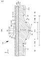
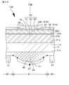
- FIG. 1 is a schematic partial cross-sectional view of the light emitting element of the first embodiment.
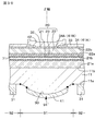
- FIG. 2 is a schematic partial cross-sectional view of a light emitting element array composed of a plurality of light emitting elements according to the first embodiment.
- FIG. 3 is a schematic partial cross-sectional view of a modified example-1 of the light emitting element of the first embodiment.
- FIG. 4 is a schematic partial cross-sectional view of a modification 2 of the light emitting element of the first embodiment.
- FIG. 5 is a schematic partial cross-sectional view of a modification 3 of the light emitting element of the first embodiment.
- FIG. 6 is a schematic partial cross-sectional view of a modified example -4 of the light emitting element of the first embodiment.
- FIG. 7 is a schematic partial cross-sectional view of a modified example 5 of the light emitting element of the first embodiment.
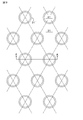
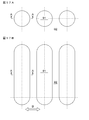
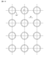
- FIG. 8 is a schematic plan view of the arrangement of the first light reflecting layer and the first electrode in the light emitting element array composed of the plurality of light emitting elements of the first embodiment.
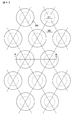
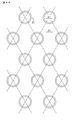
- FIG. 9 is a schematic plan view of the arrangement of the first light reflecting layer and the first electrode in the light emitting element array composed of the plurality of light emitting elements of the first embodiment.
- 10A and 10B are schematic partial end views of a laminated structure or the like for explaining the method of manufacturing the light emitting element of the first embodiment.
- FIG. 11 is a schematic partial end view of a laminated structure or the like for explaining the method of manufacturing the light emitting element of the first embodiment, following FIG. 10B.
- FIG. 12 is a schematic partial end view of a laminated structure or the like for explaining the method of manufacturing the light emitting element of the first embodiment, following FIG. 11.
- 13A and 13B are schematic partial end views of the first compound semiconductor layer and the like for explaining the method for manufacturing the light emitting device of the first embodiment, following FIG. 12.
- 14A and 14B are schematic partial end views of the first compound semiconductor layer and the like for explaining the method for manufacturing the light emitting device of the first embodiment, following FIG. 13B.
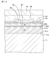
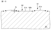
- FIG. 15 is a schematic partial end view of a first compound semiconductor layer or the like for explaining the method for manufacturing the light emitting device of the first embodiment, following FIG. 14B.
- FIG. 16A and 16B are schematic partial end views of the first compound semiconductor layer and the like for explaining the method for manufacturing the light emitting device of the second embodiment, following FIG. 13B.
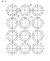
- 17A and 17B are schematic plan views showing the arrangement of the first region and the second region of the base surface in the light emitting element array of the third embodiment.
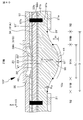
- FIG. 18 is a schematic partial end view of the light emitting element of the fourth embodiment.
- FIG. 19 is a schematic partial end view of the light emitting element of the fifth embodiment.
- FIG. 20 is a schematic partial end view of a modified example of the light emitting element of the fifth embodiment.
- 21A, 21B, and 21C are schematic partial end views of a laminated structure or the like for explaining the method of manufacturing the light emitting element of the sixth embodiment.
- FIG. 22 is a schematic partial end view of the light emitting element of the ninth embodiment.
- 23A and 23B are schematic partial end views of a laminated structure or the like for explaining the method of manufacturing the light emitting element of the ninth embodiment.
- (A), (B), and (C) of FIG. 24 are conceptual diagrams showing the light field intensities of the conventional light emitting element, the light emitting element of Example 9, and the light emitting element of Example 14, respectively.
- FIG. 25 is a schematic partial end view of the light emitting element of the tenth embodiment.
- FIG. 26 is a schematic partial end view of the light emitting element of the eleventh embodiment.
- FIG. 27A and 27B are a schematic partial end view of the light emitting element of Example 12 and a schematic partial cross-sectional view of a main part of the light emitting element of Example 12, respectively.
- FIG. 28 is a schematic partial end view of the light emitting element of the thirteenth embodiment.
- FIG. 29 is a schematic partial end view of the light emitting element of Example 14.
- FIG. 30 is a schematic partial cross-sectional view of the light emitting element of the fifteenth embodiment.
- FIG. 31 is a diagram in which a schematic partial cross-sectional view of the light emitting element of the fifteenth embodiment and two vertical modes of the vertical mode A and the vertical mode B are superimposed.
- FIG. 32 is a schematic partial cross-sectional view of the light emitting element of Example 18.
- FIG. 28 is a schematic partial end view of the light emitting element of the thirteenth embodiment.
- FIG. 29 is a schematic partial end view of the light emitting element of Example 14.
- FIG. 30 is a schematic partial cross-sectional view
- FIG. 33 is a schematic partial cross-sectional view of the light emitting element of the nineteenth embodiment.
- FIG. 34 is a schematic partial cross-sectional view of the modified example-1 of the light emitting element of the nineteenth embodiment.
- FIG. 35 is a schematic partial cross-sectional view of a light emitting element array configured according to the modification 1 of the light emitting element of the nineteenth embodiment.
- FIG. 36 is a schematic partial cross-sectional view of Modification 2 of the light emitting element of Example 19.
- FIG. 37 is a schematic partial cross-sectional view of a light emitting element array configured according to Modification 2 of the light emitting element of Example 19.
- FIG. 38 is a schematic partial cross-sectional view of Modification 3 of the light emitting element of Example 19.
- FIG. 39 is a schematic partial cross-sectional view of Modification 4 of the light emitting element of Example 19.
- FIG. 40 is a schematic partial cross-sectional view of Modification 5 of the light emitting element of Example 19.
- FIG. 41 is a schematic plan view showing the arrangement of the first light reflecting layer and the partition wall in the light emitting element array composed of the light emitting elements of Example 19.
- FIG. 42 is a schematic plan view showing the arrangement of the first light reflecting layer and the first electrode in the light emitting element array configured from the modified example-1 of the light emitting element of Example 19 shown in FIG. 41.
- FIG. 43 is a schematic plan view showing the arrangement of the first light reflecting layer and the partition wall in the light emitting element array composed of the light emitting elements of Example 19.
- FIG. 44 is a schematic plan view showing the arrangement of the first light reflecting layer and the first electrode in the light emitting element array configured from the modified example-1 of the light emitting element of Example 19 shown in FIG. 43.
- FIG. 45 is a schematic plan view showing the arrangement of the first light reflecting layer and the partition wall in the light emitting element array composed of the light emitting elements of Example 19.
- FIG. 46 is a schematic plan view showing the arrangement of the first light reflecting layer and the first electrode in the light emitting element array configured from the modified example-1 of the light emitting element of Example 19 shown in FIG. 45.
- FIG. 47 is a schematic plan view showing the arrangement of the first light reflecting layer and the partition wall in the light emitting element array composed of the light emitting elements of Example 19.
- FIG. 48 is a schematic plan view showing the arrangement of the first light reflecting layer and the first electrode in the light emitting element array configured from the modified example-1 of the light emitting element of Example 19 shown in FIG. 47.
- FIG. 49 is a conceptual diagram assuming a Fabry-Perot type resonator sandwiched between two concave mirror portions having the same radius of curvature.
- FIG. 50 is a graph showing the relationship between the value of ⁇ 0, the value of the cavity length L OR , and the value of the radius of curvature R 1 ( RD BR) of the concave mirror portion of the first light reflecting layer.
- 51 is a graph showing the relationship between the value of ⁇ 0, the value of the cavity length L OR , and the value of the radius of curvature R 1 ( RD BR) of the concave mirror portion of the first light reflecting layer.
- 52A and 52B are diagrams schematically showing the condensed state of the laser beam when the value of ⁇ 0 is “positive” and the laser beam when the value of ⁇ 0 is “negative”, respectively. It is a figure which shows typically the condensing state of.
- 53A and 53B are conceptual diagrams schematically showing the longitudinal modes existing in the gain spectrum determined by the active layer.
- FIG. 54 is a schematic partial end view of a conventional light emitting element.
- Example 1 (light emitting element according to the first to second aspects of the present disclosure, a method for manufacturing a light emitting element according to the first aspect of the present disclosure, a light emitting element having the first configuration). 3.
- Example 2 (Method for manufacturing a light emitting device according to the second aspect of the present disclosure) 4.
- Example 3 (Modification of Example 1 to Example 2) 5.
- Example 4 (another modification of Examples 1 to 2, a light emitting element having a second configuration) 6.
- Example 5 (Another modification of Examples 1 to 2, a light emitting device having a third configuration) 7.
- Example 6 (Modification of Example 5) 8.
- Example 7 (Modifications of Examples 1 to 6) 9.
- Example 8 (Modifications of Examples 1 to 7, light emitting element having a fourth configuration) 10.
- Example 9 (Modifications of Examples 1 to 8, light emitting device having the fifth A configuration) 11.
- Example 10 (Modification of Example 9, light emitting device having the fifth B configuration) 12.
- Example 11 (Modifications of Examples 9 to 10, light emitting device having the fifth-C configuration) 13.
- Example 12 (Modifications of Examples 9 to 11, light emitting elements having a fifth-D configuration) 14.
- Example 13 (Modifications of Examples 9 to 12) 15.
- Example 14 (Modifications of Examples 1 to 13, a light emitting element having a sixth-A configuration, a light emitting element having a sixth-B configuration, a light emitting element having a sixth-C configuration, and a light emitting element having a sixth-D configuration). 16.
- Example 15 (Modifications of Examples 1 to 14, light emitting element having a seventh configuration) 17.
- Example 16 (Modification of Example 15) 18.
- Example 17 (Another variant of Example 15) 19.
- Example 18 (Modifications of Examples 15 to 17) 20.
- Example 19 (Modifications of Examples 1 to 18) 21.
- Other components of Examples 1 to 18 21.
- the method for manufacturing the light emitting element according to the first to second aspects of the present disclosure In the method for manufacturing a light emitting device according to the first aspect of the present disclosure, in the convex portion forming step, a first sacrificial layer having a convex surface is formed on a region where the first region of the base surface is to be formed. After the formation, the first sacrificial layer can be used as an etching mask and etched back from the base surface toward the inside thereof.
- the first sacrificial layer / cambium is patterned, and then patterned.
- the first sacrificial layer having a convex surface can be formed.
- a first sacrificial layer having a convex surface can be formed based on the nanoimprint method.
- the method of forming the first sacrificial layer having a convex surface is not particularly limited to these methods, and it is not essential to form the first sacrificial layer having a convex surface.
- the second sacrificial layer is used as an etching mask. It can be used as an etch back from the base surface toward the inside thereof.
- the etching back step after forming the second sacrificial layer once or twice or more, the second sacrificial layer is used as an etching mask and the step of etching back from the base surface toward the inside is repeated. can do.
- the second sacrificial layer is formed a plurality of times in the etchback step, and then the second sacrificial layer and the first sacrificial layer are etched. It can be used as a mask to etch back from the base surface toward the inside thereof.
- a second sacrificial layer is formed on the entire surface, and then the second sacrificial layer is formed.
- the number of times the second sacrificial layer is formed on the entire surface may be once or may be two or more.
- the first region on the base surface on which the first light reflecting layer should be formed is formed.
- It can be in the form of forming a first sacrificial layer having a convex surface.
- a first sacrificial layer having a convex surface can be formed based on the nanoimprint method.
- the method of forming the first sacrificial layer having a convex surface is not particularly limited to these methods, and it is not essential to form the first sacrificial layer having a convex surface.
- the first sacrificial layer and the second sacrificial layer can be composed of an organic material such as a resist material, a ceramic material such as SOG, a semiconductor metal material, and the like.
- the angle (contact angle ⁇ E ) formed by the fluid and the substrate when the fluid is dropped onto a flat substrate can be expressed by the following equation.
- ⁇ Interface energy between fluid and air (corresponding to surface tension at the interface)
- ⁇ so Interface energy between the substrate and air (the surface tension of the substrate, which corresponds to the force to expand the fluid)
- ⁇ sl Interface energy between the substrate and the fluid (surface tension between the substrate and the fluid, which corresponds to a force that tries to prevent the interface between the substrate and the fluid from expanding and increasing the energy. ) Is.
- the contact angle ⁇ E between the fluid and the substrate is limited by the physical properties of the fluid and the substrate.
- the contact angle ⁇ E is rarely 10 degrees or less, and it is not easy to set the complementary angle ⁇ CA to a smaller value (for example, 10 degrees or less).
- a light emitting device according to the first to second aspects of the present disclosure, and a light emitting device manufactured by a method for manufacturing a light emitting element according to the first to second aspects of the present disclosure including the preferred modes described above.
- the complementary angle ⁇ CA can be in the form of 1 degree or more and 10 degrees or less, preferably 1 degree or more and 6 degrees or less.
- the second curve is represented by the function F (X), the intersection of the first region (1-B region) and the second region is the origin (0,0), and the second curve is composed of the second region.
- F (X) the intersection of the first region (1-B region) and the second region is the origin (0,0)
- the second curve is composed of the second region.
- the X-axis is a straight line passing through the origin (0,0)
- the angle at which the tangent of F (X) at the origin (0,0) forms with the X-axis is ⁇ CA.
- the curve may also include a line segment.
- a light emitting device including the above preferred embodiment, a light emitting device according to a second aspect of the present disclosure, and a first to second aspects of the present disclosure including the preferred embodiment described above.
- a light emitting element manufactured by the method for manufacturing a light emitting element according to the above hereinafter, these light emitting elements may be collectively referred to as "light emitting element or the like of the present disclosure"
- the top of the first region of the base surface In a light emitting element manufactured by the method for manufacturing a light emitting element according to the above (hereinafter, these light emitting elements may be collectively referred to as "light emitting element or the like of the present disclosure"), the top of the first region of the base surface.
- the radius of curvature R 1 of the above can be in the form of 1.5 ⁇ 10 -5 m or more and 2 ⁇ 10 -4 m or less.
- the height (arrow height) H 1 of the first region with respect to the flat surface of the second region is 1 ⁇ m or more and 5 ⁇ m or less. be able to.
- the radius of curvature of the top of the first region (first 1-A region) of the base surface is R 1
- the resonator length of the light emitting element is L OR.
- the diameter D 1 of the first region of the base surface is 3 ⁇ 10 -6 m or more and 1 ⁇ 10 -4 m or less. can do.
- S ⁇ (D 1/2 ) 2
- D 1 be the diameter.
- the diameter D 1 of the first 1-A region of the base surface ' is, 2 ⁇ 10 -6 m or more, it can be a 9 ⁇ 10 -5 m or less is the form, 0.1 ⁇ D 1 '/ D 1 ⁇ 1 It is preferable to satisfy.
- smooth is an analytical term. For example, if the real variable function f (x) is differentiable in a ⁇ x ⁇ b and f'(x) is continuous, it can be said that it is sloganally continuously differentiable, and it is smooth. Be expressed.
- the first light reflecting layer is formed at least in the 1-A region of the base surface, but the extending portion of the first light reflecting layer is formed in the 1-B region of the base surface. In some cases, the first light reflecting layer is not formed in the 1-B region. Further, when the extending portion of the first light reflecting layer is formed in the first 1-B region of the base surface, the extending portion of the first light reflecting layer is formed in the second region of the base surface occupying the peripheral region. In some cases, the extending portion of the first light reflecting layer is not formed in the second region.
- the first surface of the first compound semiconductor layer may form a base surface.
- a light emitting element having such a configuration is referred to as a "first configuration" for convenience.
- the compound semiconductor substrate may be arranged between the first surface of the first compound semiconductor layer and the first light reflecting layer, and the base surface may be composed of the surface of the compound semiconductor substrate. it can.
- a light emitting element having such a configuration is referred to as a "light emitting element having a second configuration" for convenience.
- the compound semiconductor substrate can be configured to consist of a GaN substrate.
- any of a polar substrate, a semipolar substrate, and a non-polar substrate may be used.
- the thickness of the compound semiconductor substrate can be 5 ⁇ 10 -5 m to 1 ⁇ 10 -4 m, but the thickness is not limited to such a value.
- a base material is arranged between the first surface of the first compound semiconductor layer and the first light reflecting layer, or the first surface of the first compound semiconductor layer and the first light reflecting layer.
- a compound semiconductor substrate and a base material are arranged between them, and the base surface can be configured to be composed of the surface of the base material.
- a light emitting element having such a configuration is referred to as a "light emitting element having a third configuration" for convenience.
- the material constituting the base material include transparent dielectric materials such as TiO 2 , Ta 2 O 5 , and SiO 2 , silicone-based resins, and epoxy-based resins.
- the material constituting various compound semiconductor layers (including the compound semiconductor substrate) located between the active layer and the first light reflecting layer may be used. It is preferable that there is no modulation of the refractive index of 10% or more (there is no difference in the refractive index of 10% or more based on the average refractive index of the laminated structure), which causes disturbance of the optical field in the resonator. Can be suppressed.
- the value of the thermal conductivity of the laminated structure can be a form higher than the value of the thermal conductivity of the first light reflecting layer. ..
- the value of the thermal conductivity of the dielectric material constituting the first light reflecting layer is generally about 10 watts / (m ⁇ K) or less.
- the value of the thermal conductivity of the GaN-based compound semiconductor constituting the laminated structure is about 50 watts / (m ⁇ K) to about 100 watts / (m ⁇ K).
- the figure (first curve) drawn by the 1st-A region when the 1st-A region is cut in the virtual plane including the stacking direction of the laminated structure can be a part of a circle, a part of a parabola, a part of a sine curve, a part of an ellipse, a part of a catenary curve.
- the shape may not be exactly part of a circle, it may not be part of a parabola, it may not be part of a sine curve, it may be part of an ellipse. It may not be part of the catenary curve, or strictly it may not be part of the catenary curve.
- the figure is a part of a circle, a part of a parabola, a part of a sine curve, a part of an ellipse, a part of a catenary curve.
- the figures drawn by the 1st A region and the 1st B region are obtained by measuring the shapes of the 1st A region and the 1st B region with a measuring instrument and analyzing the obtained data based on the least squares method. You can ask.
- the second curve is composed of at least one kind of figure selected from a group consisting of a downwardly convex curve, a line segment, and an arbitrary combination of curves.
- a "downwardly convex curve” is used.
- the "arbitrary combination of curves" includes line segments and upwardly convex curves.
- connection between the first curve and the second curve, or the connection between a plurality of curves when the second curve is composed of a plurality of curves and the like may be continuous in terms of analysis. It may be smooth (ie, it may be differentiable), it may be analytically discontinuous, and the connections may not be smooth (ie, non-differentiable). There may be).
- the first curve is connected to any combination of a downwardly convex curve, a line segment, and an arbitrary curve, and a downwardly convex curve, a line segment, and an arbitrary curve.
- Any of the combinations further means that it is connected to any of a downwardly convex curve, a line segment, or any combination of curves (but not the same curve, etc.).
- a surface emitting laser element (vertical resonator laser, VCSEL) that emits laser light through the first light reflecting layer can be configured by the light emitting element or the like of the present disclosure including the preferred form described above, or It is also possible to configure a surface emitting laser element that emits laser light through the second light reflecting layer. In some cases, the light emitting element manufacturing substrate (described later) may be removed.
- the formation pitch of the light emitting elements (the adjacent light emitting elements are arranged from the axis of the first light reflecting layer constituting the light emitting element).
- the distance to the axis of the first light reflecting layer is preferably 3 ⁇ m or more and 50 ⁇ m or less, preferably 5 ⁇ m or more and 30 ⁇ m or less, and more preferably 8 ⁇ m or more and 25 ⁇ m or less.
- the central portion (top) of the first light reflecting layer of each light emitting element is not limited, but is located on the apex (intersection) of the square lattice. It can be, or it can be in the form of being located on the apex (intersection) of an equilateral triangle grid.
- the laminated structure is at least one kind of material selected from the group consisting of a GaN-based compound semiconductor, an InP-based compound semiconductor, and a GaAs-based compound semiconductor. It can be composed of.
- the laminated structure (A) Structure made of GaN-based compound semiconductor (b) Structure made of InP-based compound semiconductor (c) Structure made of GaAs-based compound semiconductor (d) Structure made of GaN-based compound semiconductor and InP-based compound semiconductor (e) GaN-based Configuration of compound semiconductors and GaAs-based compound semiconductors (f) Configuration of InP-based compound semiconductors and GaAs-based compound semiconductors (g) Configuration of GaN-based compound semiconductors, InP-based compound semiconductors, and GaAs-based compound semiconductors. ..
- the laminated structure can be more specifically composed of, for example, an AlInGaN-based compound semiconductor.
- AlInGaN-based compound semiconductor more specifically, GaN, AlGaN, InGaN, and AlInGaN can be mentioned.
- these compound semiconductors may contain a boron (B) atom, a thallium (Tl) atom, an arsenic (As) atom, a phosphorus (P) atom, and an antimony (Sb) atom, if desired. ..
- the active layer preferably has a quantum well structure.
- the active layer having a quantum well structure has a structure in which at least one well layer and a barrier layer are laminated, but as a combination of (compound semiconductors constituting the well layer and compound semiconductors constituting the barrier layer), ( In y Ga (1-y) N, GaN), (In y Ga (1-y) N, In z Ga (1-z) N) [However, y> z], (In y Ga (1-y) ) N, AlGaN) can be exemplified.
- the first compound semiconductor layer is composed of a first conductive type (for example, n type) compound semiconductor
- the second compound semiconductor layer is made of a second conductive type (for example, p type) compound semiconductor different from the first conductive type.
- the first compound semiconductor layer and the second compound semiconductor layer are also referred to as a first clad layer and a second clad layer.
- the first compound semiconductor layer and the second compound semiconductor layer may be a layer having a single structure, a layer having a multilayer structure, or a layer having a superlattice structure. Further, it may be a layer provided with a composition gradient layer and a concentration gradient layer.
- gallium (Ga), indium (In), and aluminum (Al) can be mentioned as group III atoms constituting the laminated structure
- arsenic (As) can be mentioned as the group V atoms constituting the laminated structure.
- GaNAs, GaInNAs, and examples of the compound semiconductor constituting the active layer include GaAs, AlGaAs, GaInAs, GaInAsP, GaInP, GaSb, GaAsSb, GaN, InN, GaInN, GaInNAs, and GaInNAsSb.
- the quantum well structure examples include a two-dimensional quantum well structure, a one-dimensional quantum well structure (quantum wire), and a zero-dimensional quantum well structure (quantum dot).
- Materials constituting the quantum well include, for example, Si; Se; calcopyrite compounds CIGS (CuInGaSe), CIS (CuInSe 2 ), CuInS 2 , CuAlS 2 , CuAlSe 2 , CuGaS 2 , CuGaSe 2 , AgAlS 2 , AgAlSe.
- Perovskite-based material Perovskite-based material; Group III-V compounds GaAs, GaP, InP, AlGaAs, InGaP, AlGaInP, InGaAsP, GaN, InAs, InGaAs, GaInNAs, GaSb, GaAsSb; CdSe, CdSe, Cd , CdTe, In 2 Se 3 , In 2 S 3 , Bi 2 Se 3 , Bi 2 S 3 , ZnSe, ZnTe, ZnS, HgTe, HgS, PbSe, PbS, TiO 2, etc., but are limited to these. It is not something to do.
- the laminated structure is formed on the second surface of the light emitting device manufacturing substrate, or is also formed on the second surface of the compound semiconductor substrate.
- the second surface of the light emitting device manufacturing substrate or the compound semiconductor substrate faces the first surface of the first compound semiconductor layer, and the first surface of the light emitting element manufacturing substrate or the compound semiconductor substrate is the light emitting element manufacturing substrate. Facing the second surface of.
- GaN substrate As substrates for manufacturing light emitting elements, GaN substrate, sapphire substrate, GaAs substrate, SiC substrate, alumina substrate, ZnS substrate, ZnO substrate, AlN substrate, LiMgo substrate, LiGaO 2 substrate, MgAl 2 O 4 substrate, InP substrate, Si substrate, Examples thereof include those having a base layer and a buffer layer formed on the surface (main surface) of these substrates, but the use of a GaN substrate is preferable because the defect density is low. Further, examples of the compound semiconductor substrate include a GaN substrate, an InP substrate, and a GaAs substrate.
- any main surface (second surface) of the GaN substrate can be used for forming a compound semiconductor layer. ..
- the main surface of the GaN substrate depending on the crystal structure (for example, cubic type, hexagonal type, etc.), names such as so-called A-plane, B-plane, C-plane, R-plane, M-plane, N-plane, S-plane, etc. It is also possible to use the crystal plane orientation referred to in (1), or a plane in which these are turned off in a specific direction.
- an organic metal chemical vapor deposition method MOCVD method, Metal Organic-Chemical Vapor Deposition method, MOVPE method, Metal Organic-Vapor Phase Epitaxy method
- MOCVD method Metal Organic-Chemical Vapor Deposition method
- MOVPE method Metal Organic-Vapor Phase Epitaxy method
- MBE method molecule Molecular beam epitaxy method
- HVPE method hydride vapor phase growth method in which halogen contributes to transport or reaction
- ALD method Atomic Layer Deposition method
- MEE method migration enhanced epitaxy method
- MEE method MEE method
- Migration-Enhanced Epitaxy method plasma assisted physical vapor deposition method
- PPD method plasma assisted physical vapor deposition method
- the GaAs and InP materials also have a sphalerite structure.
- the main surface of the compound semiconductor substrate composed of these materials include surfaces turned off in a specific direction in addition to surfaces such as (100), (111) AB, (211) AB, and (311) AB. it can.
- "AB” means that the 90 ° off direction is different, and whether the main material of the surface is group III or group V is determined by this off direction.
- the film forming method the MBE method, the MOCVD method, the MEE method, the ALD method and the like are generally used as in the GaN system, but the film forming method is not limited to these methods.
- trimethylgallium (TMG) gas and triethylgallium (TEG) gas can be mentioned as the organic gallium source gas in the MOCVD method, and ammonia as the nitrogen source gas. Gas and hydrazine gas can be mentioned.
- silicon (Si) may be added as an n-type impurity (n-type dopant)
- the GaN-based compound semiconductor having a p-type conductive type may be added.
- magnesium (Mg) may be added as a p-type impurity (p-type dopant).
- trimethylaluminum (TMA) gas may be used as the Al source, or trimethylindium (TMI) gas may be used as the In source.
- TMA trimethylaluminum
- TMI trimethylindium
- monosilane gas (SiH 4 gas) may be used as the Si source
- biscyclopentadienyl magnesium gas, methylcyclopentadienyl magnesium, or biscyclopentadienyl magnesium (Cp 2 Mg) may be used as the Mg source. Good.
- n-type impurities n-type dopants
- p-type impurities p-type dopants
- Mg, Zn, Cd, Be, Ca, Ba, C, Hg, and Sr can be mentioned.
- organometallic raw materials such as TMGa, TEGa, TMIn, and TMAl are generally used as the group III raw materials.
- group V raw material arsine gas (AsH 3 gas), phosphine gas (PH 3 gas), ammonia (NH 3 ) and the like are used.
- group V raw material an organic metal raw material may be used, and examples thereof include tertiary butylarsine (TBAs), tertiary butylphosphine (TBP), dimethylhydrazine (DMHy), and trimethylantimony (TMSb). Can be done.
- n-type dopant monosilane (SiH 4 ) is used as the Si source, hydrogen selenide (H 2 Se) or the like is used as the Se source.
- p-type dopant dimethylzinc (DMZn), biscyclopentadienyl magnesium (Cp 2 Mg) and the like are used.
- DMZn dimethylzinc
- Cp 2 Mg biscyclopentadienyl magnesium
- the laminated structure is formed on the second surface of the light emitting device manufacturing substrate, or is also formed on the second surface of the compound semiconductor substrate.
- the second surface of the light emitting device manufacturing substrate or the compound semiconductor substrate faces the first surface of the first compound semiconductor layer, and the first surface of the light emitting element manufacturing substrate or the compound semiconductor substrate is the light emitting element manufacturing substrate. Facing the second surface of.
- GaN substrate As substrates for manufacturing light emitting elements, GaN substrate, sapphire substrate, GaAs substrate, SiC substrate, alumina substrate, ZnS substrate, ZnO substrate, AlN substrate, LiMgo substrate, LiGaO 2 substrate, MgAl 2 O 4 substrate, InP substrate, Si substrate, Examples thereof include those having a base layer and a buffer layer formed on the surface (main surface) of these substrates, but the use of a GaN substrate is preferable because the defect density is low. Further, examples of the compound semiconductor substrate include a GaN substrate, an InP substrate, and a GaAs substrate.
- any main surface (second surface) of the GaN substrate can be used for forming a compound semiconductor layer. ..
- the main surface of the GaN substrate depending on the crystal structure (for example, cubic type, hexagonal type, etc.), names such as so-called A-plane, B-plane, C-plane, R-plane, M-plane, N-plane, S-plane, etc. It is also possible to use the crystal plane orientation referred to in (1), or a plane in which these are turned off in a specific direction.
- an organic metal chemical vapor deposition method MOCVD method, Metal Organic-Chemical Vapor Deposition method, MOVPE method, Metal Organic-Vapor Phase Epitaxy method
- MOCVD method Metal Organic-Chemical Vapor Deposition method
- MOVPE method Metal Organic-Vapor Phase Epitaxy method
- MBE method molecule Molecular beam epitaxy method
- HVPE method hydride vapor phase growth method in which halogen contributes to transport or reaction
- ALD method Atomic Layer Deposition method
- MEE method migration enhanced epitaxy method
- MEE method MEE method
- Migration-Enhanced Epitaxy method plasma assisted physical vapor deposition method
- PPD method plasma assisted physical vapor deposition method
- the substrate for manufacturing the light emitting device may be left as it is, or the active layer, the second compound semiconductor layer, the second electrode, and the second light reflecting layer may be left on the first compound semiconductor layer. May be sequentially formed, and then the light emitting element manufacturing substrate may be removed. Specifically, an active layer, a second compound semiconductor layer, a second electrode, and a second light-reflecting layer were sequentially formed on the first compound semiconductor layer, and then the second light-reflecting layer was fixed to a support substrate. After that, the substrate for manufacturing the light emitting element may be removed to expose the first compound semiconductor layer (the first surface of the first compound semiconductor layer).
- an alkaline aqueous solution such as a sodium hydroxide aqueous solution or a potassium hydroxide aqueous solution, an ammonia solution + hydrogen peroxide solution, a sulfuric acid solution + hydrogen peroxide solution, a hydrochloric acid solution + hydrogen peroxide solution, or a phosphoric acid solution.
- + Wet etching method using aqueous hydrogen solution chemical mechanical polishing method (CMP method), mechanical polishing method, dry etching method such as reactive ion etching (RIE) method, lift-off method using laser, etc.
- the support substrate may be composed of, for example, various substrates exemplified as a substrate for manufacturing a light emitting element, or an insulating substrate made of AlN or the like, a semiconductor substrate made of Si, SiC, Ge or the like, a metal substrate, or the like.
- a conductive substrate or a metal substrate or an alloy substrate can be used from the viewpoints of mechanical properties, elastic deformation, plastic deformability, heat dissipation, and the like. It is preferable to use it.
- As the thickness of the support substrate for example, 0.05 mm to 1 mm can be exemplified.
- solder bonding method As a method for fixing the second light reflecting layer to the support substrate, known methods such as a solder bonding method, a room temperature bonding method, a bonding method using an adhesive tape, a bonding method using a wax bonding, and a method using an adhesive are used. Although it can be used, it is desirable to adopt a solder bonding method or a room temperature bonding method from the viewpoint of ensuring conductivity.
- a silicon semiconductor substrate which is a conductive substrate
- the bonding temperature may be 400 ° C. or higher.
- the first electrode electrically connected to the first compound semiconductor layer is common to a plurality of light emitting elements
- the second electrode electrically connected to the second compound semiconductor layer is common to a plurality of light emitting elements. Yes, or it can be in the form of being individually provided in a plurality of light emitting elements.
- the first electrode may be formed on the first surface facing the second surface of the light emitting element manufacturing substrate, or may be formed on the second surface of the compound semiconductor substrate. It may be formed on the first surface facing the above surface.
- the light emitting element manufacturing substrate is not left, it may be formed on the first surface of the first compound semiconductor layer constituting the laminated structure.
- the first electrode since the first light reflecting layer is formed on the first surface of the first compound semiconductor layer, for example, the first electrode may be formed so as to surround the first light reflecting layer.
- the first electrode is, for example, gold (Au), silver (Ag), palladium (Pd), platinum (Pt), nickel (Ni), Ti (titanium), vanadium (V), tungsten (W), chromium (Cr). ), Al (aluminum), Cu (copper), Zn (zinc), tin (Sn) and indium (In), including at least one metal (including alloy) selected from the group. It is desirable to have a multi-layer structure, specifically, for example, Ti / Au, Ti / Al, Ti / Al / Au, Ti / Pt / Au, Ni / Au, Ni / Au / Pt, Ni / Pt, Pd.
- the first electrode can be formed by a PVD method such as a vacuum vapor deposition method or a sputtering method.
- the first electrode When the first electrode is formed so as to surround the first light reflecting layer, the first light reflecting layer and the first electrode can be in contact with each other. Alternatively, the first light reflecting layer and the first electrode can be separated from each other. In some cases, a state in which the first electrode is formed on the edge of the first light reflecting layer and a state in which the first light reflecting layer is formed on the edge of the first electrode are mentioned. You can also.
- planar shapes of the first light reflecting layer, the first region, the 1-A region, the 1-B region, and the second light reflecting layer are specifically circular, elliptical, oval, rectangular, and regular polygon. (Regular triangle, square, regular hexagon, etc.) can be mentioned.
- the second electrode can be made of a transparent conductive material.
- an indium-based transparent conductive material specifically, for example, indium-tin oxide (ITO, Indium Tin Oxide, Sn-doped In 2 O 3 , crystalline ITO and Including amorphous ITO), indium-zinc oxide (IZO, Indium Zinc Oxide), indium-gallium oxide (IGO), indium-doped gallium-zinc oxide (IGZO, In-GaZnO 4 ), IFO (F-doped) in 2 O 3) of, ITiO (Ti-doped in 2 O 3), InSn, InSnZnO], the tin-based transparent conductive material [specifically, for example, tin oxide (SnO X), SnO of ATO (Sb-doped 2 ), FTO (F-doped SnO 2 )], zinc-based transparent conductive material [specifically, for example, zinc
- Dope zinc oxide (GZO), AlMgZnO (aluminum oxide and magnesium oxide-doped zinc oxide)], NiO, TiO X , graphene can be exemplified.
- a transparent conductive film having a gallium oxide, titanium oxide, niobium oxide, antimony oxide, nickel oxide or the like as a base layer can be mentioned, and a spinel-type oxide, YbFe 2
- a transparent conductive material such as an oxide having an O 4 structure can also be mentioned.
- the material constituting the second electrode depends on the arrangement state of the second light reflecting layer and the second electrode, but is not limited to the transparent conductive material, and palladium (Pd), platinum (Pt), and the like.
- the second electrode may be composed of at least one of these materials.
- the second electrode can be formed by a PVD method such as a vacuum vapor deposition method or a sputtering method.
- a low-resistance semiconductor layer can be used as the transparent electrode layer, and in this case, specifically, an n-type GaN-based compound semiconductor layer can also be used.
- the electrical resistance at the interface can be reduced by joining the two via a tunnel junction.
- a first pad electrode and a second pad electrode are provided on the first electrode and the second electrode in order to electrically connect to an external electrode or circuit (hereinafter, may be referred to as "external circuit or the like"). You may.
- the pad electrode is a single layer containing at least one metal selected from the group consisting of Ti (titanium), aluminum (Al), Pt (platinum), Au (gold), Ni (nickel), Pd (palladium). It is desirable to have a configuration or a multi-layer configuration.
- the pad electrode has a Ti / Pt / Au multi-layer structure, a Ti / Au multi-layer structure, a Ti / Pd / Au multi-layer structure, a Ti / Pd / Au multi-layer structure, and a Ti / Ni / Au multi-layer structure.
- the multilayer configuration exemplified by the multilayer configuration of Ti / Ni / Au / Cr / Au can also be used.
- a cover metal layer made of, for example, Ni / TiW / Pd / TiW / Ni is formed on the surface of the first electrode, and a cover metal layer is formed on the cover metal layer.
- the light reflecting layer (distributed Bragg reflector layer, distributed Bragg Reflector layer, DBR layer) constituting the first light reflecting layer and the second light reflecting layer is composed of, for example, a semiconductor multilayer film or a dielectric multilayer film.
- the dielectric material for example, Si, Mg, Al, Hf , Nb, Zr, Sc, Ta, Ga, Zn, Y, B, oxides such as Ti, nitrides (e.g., SiN X, AlN X, AlGaN X , GaN X , BN X, etc.), or fluoride and the like.
- the light reflecting layer can be obtained by alternately laminating two or more kinds of dielectric films made of dielectric materials having different refractive indexes among these dielectric materials.
- each dielectric film may be appropriately selected.
- the thickness of each dielectric film, a material or the like to be used, as appropriate, can be adjusted, the oscillation wavelength (emission wavelength) lambda 0, is determined by the refractive index n of the oscillation wavelength lambda 0 of the material used. Specifically, it is preferably an odd multiple of ⁇ 0 / (4n).
- the light-emitting element of the oscillation wavelength lambda 0 is 410 nm
- when forming the light reflecting layer from SiO X / NbO Y it may be exemplified about 40nm to 70 nm.
- the number of layers can be exemplified by 2 or more, preferably about 5 to 20.
- As the thickness of the entire light reflecting layer for example, about 0.6 ⁇ m to 1.7 ⁇ m can be exemplified. Further, it is desirable that the light reflectance of the light reflecting layer is 95% or more.
- the size and shape of the light reflecting layer are not particularly limited as long as they cover the current injection region or the element region (which will be described later).
- the light reflecting layer can be formed based on a well-known method, and specifically, for example, a vacuum vapor deposition method, a sputtering method, a reactive sputtering method, an ECR plasma sputtering method, a magnetron sputtering method, an ion beam assisted vapor deposition method, and the like.
- PVD method such as ion plating method, laser ablation method; various CVD methods; coating method such as spray method, spin coating method, dip method; method of combining two or more of these methods; these methods and whole or partial Pretreatment, irradiation of inert gas (Ar, He, Xe, etc.) or plasma, irradiation of oxygen gas, ozone gas, plasma, oxidation treatment (heat treatment), exposure treatment, etc. Can be mentioned.
- inert gas Ar, He, Xe, etc.
- plasma irradiation of oxygen gas, ozone gas, plasma, oxidation treatment (heat treatment), exposure treatment, etc.
- a current injection area is provided to regulate the current injection into the active layer.
- the shape of the boundary between the current injection region and the current non-injection / inner region, the shape of the boundary between the current non-injection / inner region and the current non-injection / outer region, and the planar shape of the opening provided in the element region or the current constriction region Specific examples thereof include circles, ellipses, oval, rectangles, and regular polygons (regular triangles, squares, regular hexagons, etc.). It is desirable that the shape of the boundary between the current injection region and the current non-injection / inner region and the shape of the boundary between the current non-injection / inner region and the current non-injection / outer region are similar figures or approximate shapes.
- the "element region” is a region in which a narrowed current is injected, a region in which light is confined due to a difference in refractive index, or is sandwiched between a first light reflecting layer and a second light reflecting layer. It refers to a region in which laser oscillation occurs, or a region sandwiched between the first light reflecting layer and the second light reflecting layer, which actually contributes to laser oscillation.
- bumps may be arranged on the second surface of the light emitting element (exposed surface of the light emitting element on the second light reflecting layer side).
- the bumps include gold (Au) bumps, solder bumps, and indium (In) bumps, and the method of arranging the bumps can be a well-known method.
- the bump is provided on the second pad electrode provided on the second electrode, or is also provided on the extending portion of the second pad electrode.
- a brazing material can be used instead of the bump.
- brazing material for example, In (indium: melting point 157 ° C); indium-gold-based low melting point alloy; Sn 80 Ag 20 (melting point 220 to 370 ° C), Sn 95 Cu 5 (melting point 227 to 370 ° C).
- Tin (Sn) -based high-temperature solder such as Pb 97.5 Ag 2.5 (melting point 304 ° C), Pb 94.5 Ag 5.5 (melting point 304-365 ° C), Pb 97.5 Ag 1.5 Sn 1.0 (melting point 309 ° C) and other lead (melting point 309 ° C) Pb) -based high-temperature solder; tin (Zn) -based high-temperature solder such as Zn 95 Al 5 (melting point 380 ° C); Sn 5 Pb 95 (melting point 300 to 314 ° C), Sn 2 Pb 98 (melting point 316 to 322 ° C) ) Etc. tin-lead standard solder; brazing materials such as Au 88 Ga 12 (melting point 381 ° C) (all the above subscripts represent atomic%) can be exemplified.
- the side surface or the exposed surface of the laminated structure may be covered with a coating layer (insulating film).
- the coating layer (insulating film) can be formed based on a well-known method.
- the refractive index of the material constituting the coating layer (insulating film) is preferably smaller than the refractive index of the material constituting the laminated structure.
- the material constituting the coating layer (insulating film) illustrated SiO X based material containing SiO 2, SiN X-based material, SiO Y N Z material, TaO X, ZrO X, AlN X, AlO X, a GaO X
- an organic material such as a polyimide resin can be mentioned.
- a method for forming the coating layer (insulating film) for example, a PVD method such as a vacuum deposition method or a sputtering method, a CVD method, or a coating method can be used for forming the coating layer (insulating film).
- Example 1 relates to a light emitting element according to the first to second aspects of the present disclosure, a light emitting element having a first configuration, and a method for manufacturing a light emitting element according to the first aspect of the present disclosure.
- a schematic partial cross-sectional view of the light emitting element of the first embodiment is shown in FIG. 1, and a schematic partial cross-sectional view of the light emitting element array in which a plurality of the light emitting elements of the first embodiment are arranged is shown in FIG. 8 and 9 show schematic plan views of the arrangement of the first light reflecting layer and the first electrode in the element array.
- FIG. 8 shows a case where the light emitting element is located on the apex (intersection) of the square lattice
- FIG. 9 shows a case where the light emitting element is located on the apex (intersection) of the equilateral triangle lattice.
- FIG. 2 or FIG. 3, FIG. 4, FIG. 5, FIG. 6 and FIG. 7, which will be described later, are schematic partial cross-sectional views taken along the arrows AA of FIG. 8 or 9.
- the Z axis indicates an axis of the first light reflecting layer constituting the light emitting element (a perpendicular line passing through the center of the first light reflecting layer and with respect to the laminated structure).
- the illustration of the second compound semiconductor layer, the second light reflecting layer, and the like is omitted.
- the light emitting element 10A of Example 1 or the light emitting elements of Examples 2 to 19 described later are A first compound semiconductor layer 21 having a first surface 21a and a second surface 21b facing the first surface 21a, The active layer (light emitting layer) 23 facing the second surface 21b of the first compound semiconductor layer 21, and A second compound semiconductor layer 22 having a first surface 22a facing the active layer 23 and a second surface 22b facing the first surface 22a, Laminated structure 20, The first light reflecting layer 41, and The second light reflecting layer 42, which is formed on the second surface side of the second compound semiconductor layer 22 and has a flat shape, Is equipped with The base surface 90 located on the first surface side of the first compound semiconductor layer 21 surrounds the first region 91 and the first region 91, which consist of protrusions protruding in a direction away from the active layer 23, and has a flat surface. It has a second region 92.
- the first region 91 is composed of a first 1-A region 91A including the top of the protrusion and a 1-B region 91B surrounding the 1-A region 91A.
- the first light reflecting layer 41 is formed on at least the 1st 1-A region 91A.
- a first structure composed of a first 1-A region 91A in the cross-sectional shape of the base surface 90 when the base surface 90 is cut in a virtual plane (for example, an XZ plane in the illustrated example) including the stacking direction of the laminated structure 20.
- the curve is composed of a smooth curve that is convex upward (that is, a smooth curve that has a convex shape toward the direction away from the active layer 23).
- a smooth curve that is, a smooth curve that has a convex shape toward the direction away from the active layer 23.
- the complementary angle of the angle formed by the second curve and this straight line is complemented.
- ⁇ CA has a value exceeding 0 degrees (specifically, 1 degree or more and 6 degrees or less).
- the second curve is from at least one type of figure selected from a group consisting of a downwardly convex curve (a curve having a convex shape toward the active layer 23), a line segment, and an arbitrary combination of curves. It is configured.
- the first light reflecting layer 41 is formed on at least the top 91'of the first region 91.
- the complementary angle ⁇ CA of the angle formed by this curve and this straight line is 1 degree or more and 6 degrees or less.
- the first compound semiconductor layer 21 has a first conductive type (specifically, n type), and the second compound semiconductor layer 22 has a second conductive type (specifically, p type) different from the first conductive type. ).
- the light emitting element of the embodiment includes a surface emitting laser element (vertical resonator laser, VCSEL) that emits laser light.
- the radius of curvature R 1 of the top portion 91 'of the first region 91 of the base surface 90 1.5 ⁇ 10 -5 m or more, desirably 2 ⁇ 10 -4 m or less, and the second region 92
- the height (arrow height) H 1 of the first region 91 with respect to the flat surface of the base surface 90 is 1 ⁇ m or more and 5 ⁇ m or less, and further, the first region 91 (1-A region 91A) of the base surface 90.
- the diameter D 1 of the first region 91 of the base surface 90 is preferably 3 ⁇ 10 -6 m or more and 1 ⁇ 10 -4 m or less, and the diameter D of the first 1-A region 91 of the base surface 90.
- 1 ', 2 ⁇ 10 -6 m or more is preferably not more than 9 ⁇ 10 -5 m, more preferably satisfies the 1 ⁇ 10 -5 m ⁇ L oR .
- the formation pitch P 0 of the light emitting element 10A is preferably 3 ⁇ m or more and 50 ⁇ m or less, preferably 5 ⁇ m or more and 30 ⁇ m or less, and more preferably 8 ⁇ m or more and 25 ⁇ m or less.
- R 1 / L OR 3.5
- the first surface 21a of the first compound semiconductor layer 21 constitutes the base surface 90. That is, the light emitting element 10A of the first embodiment is a light emitting element having the first configuration.
- the first light reflecting layer 41 is formed at least in the 1st 1-A region 91A of the base surface 90, but specifically, the first light reflecting layer 41 is formed on the base surface 90. It is formed in the 1st 1-A region 91A.
- the present invention is not limited to this, and the extending portion of the first light reflecting layer 41 may be formed in the first 1-B region 91B of the base surface 90, and further, the first light reflecting layer 41 may be formed.
- the extending portion may be formed in the second region 92 of the base surface 90 that occupies the peripheral region.
- the light emitting element 10A of the first embodiment shown in FIG. 1 corresponds to the case of (1) described above, and in the light emitting element 10A, a virtual plane including the stacking direction (Z-axis direction) of the laminated structure 20 (illustrated example). Then, for example, the figure (first curve) drawn by the 1-A region 91A when the 1-A region 91A is cut in the XZ plane) is, for example, a part of a circle.
- the second curve composed of the first 1-B region 91B is a downwardly convex curve, specifically, a part of a circle, for example.
- the connection between the first curve and the second curve (indicated by a black square) is analytically continuous and smooth (ie, differentiable).
- the connection portion between the first region 91 (first 1-B region 91B) and the second region 92 is indicated by a black circle.
- the laminated structure 20 can be composed of at least one material selected from the group consisting of a GaN-based compound semiconductor, an InP-based compound semiconductor, and a GaAs-based compound semiconductor. Specifically, in the first embodiment, the laminated structure 20 is made of a GaN-based compound semiconductor.
- the first compound semiconductor layer 21 is composed of, for example, an n-GaN layer doped with Si about 2 ⁇ 10 16 cm -3
- the active layer 23 is an In 0.04 Ga 0.96 N layer (barrier layer). It is composed of a five-layered multiple quantum well structure in which In 0.16 Ga 0.84 N layers (well layers) are laminated
- the second compound semiconductor layer 22 is, for example, p-, which is doped with magnesium by about 1 ⁇ 10 19 cm -3. It consists of a GaN layer.
- the plane orientation of the first compound semiconductor layer 21 is not limited to the ⁇ 0001 ⁇ plane, and may be, for example, a ⁇ 20-21 ⁇ plane which is a semi-polar plane.
- the first electrode 31 made of Ti / Pt / Au is electrically connected to an external circuit or the like via, for example, a first pad electrode (not shown) made of Ti / Pt / Au or V / Pt / Au.
- the second electrode 32 is formed on the second compound semiconductor layer 22, and the second light reflecting layer 42 is formed on the second electrode 32.
- the second light reflecting layer 42 on the second electrode 32 has a flat shape.
- the second electrode 32 is made of a transparent conductive material, specifically, ITO having a thickness of 30 nm.
- the pad electrode 33 may be formed or connected (see FIGS. 3 and 4).
- the first light reflecting layer 41 and the second light reflecting layer 42 have a laminated structure of a Ta 2 O 5 layer and a SiO 2 layer, or a laminated structure of a SiN layer and a SiO 2 layer. Although the first light reflecting layer 41 and the second light reflecting layer 42 have a multilayer structure in this way, they are represented by one layer for the sake of simplification of drawings.
- first electrode 31 specifically, the opening 31'provided in the first electrode 31
- first light reflecting layer 41 the first light reflecting layer 41
- second light reflecting layer 42 the insulating layer (current constriction layer) 34.
- planar shape of each of the openings 34A is circular.
- the insulating material between the second electrode 32 and the second compound semiconductor layer 22 e.g., SiO X and SiN X, AlO X
- the insulating layer (current constriction layer) 34 is provided with an opening 34A for injecting a current into the second compound semiconductor layer 22.
- the second compound semiconductor layer 22 may be etched by the RIE method or the like to form a mesa structure.
- a part of the laminated second compound semiconductor layer 22 may be partially oxidized from the lateral direction to form a current constriction region.
- an impurity for example, boron
- an impurity for example, boron
- these may be combined as appropriate.
- the second electrode 32 needs to be electrically connected to the portion (current injection region) of the second compound semiconductor layer 22 through which a current flows due to current constriction.
- the second electrode 32 is common to the light emitting elements 10A constituting the light emitting element array, and the second electrode 32 is connected to an external circuit or the like via the first pad electrode (not shown). Be connected.
- the first electrode 31 is also common to the light emitting elements 10A constituting the light emitting element array, and is connected to an external circuit or the like via the first pad electrode (not shown). Then, the light may be emitted to the outside through the first light reflecting layer 41, or the light may be emitted to the outside through the second light reflecting layer 42.
- the second electrode 32 is individually formed in the light emitting element 10A constituting the light emitting element array. It is connected to an external circuit or the like via the second pad electrode 33.
- the first electrode 31 is common to the light emitting elements 10A constituting the light emitting element array, and is connected to an external circuit or the like via the first pad electrode (not shown). Then, the light may be emitted to the outside through the first light reflecting layer 41, or the light may be emitted to the outside through the second light reflecting layer 42.
- FIG. 4 a schematic partial cross-sectional view of a modification 2 of the light emitting element 10A of the first embodiment
- the second electrode 32 is individually formed in the light emitting element 10A constituting the light emitting element array.
- a bump 35 is formed on the second pad electrode 33 formed on the second electrode 32, and is connected to an external circuit or the like via the bump 35.
- the first electrode 31 is common to the light emitting elements 10A constituting the light emitting element array, and is connected to an external circuit or the like via the first pad electrode (not shown).
- the bumps 35 are arranged on the second surface side portion of the second compound semiconductor layer 22 facing the base surface 90, and cover the second light reflecting layer 42.
- Examples of the bump 35 include a gold (Au) bump, a solder bump, and an indium (In) bump.
- the method of arranging the bumps 35 can be a well-known method. Then, the light is emitted to the outside through the first light reflecting layer 41.
- the bump 35 may be provided in the light emitting element 10A shown in FIG. Examples of the shape of the bump 35 include a cylindrical shape, an annular shape, and a hemispherical shape.
- FIG. 5 shows a schematic partial cross-sectional view of Modification 3 of the light emitting element 10A of Example 1.
- the second curve is composed of line segments.
- the connection between the first curve and the second curve (indicated by a black square) is analytically continuous and smooth (ie, differentiable).
- the connection between the first curve and the second curve is not analytically continuous and not smooth (ie, not differentiable).
- FIG. 6 shows a schematic partial cross-sectional view of a modified example -4 of the light emitting element 10A of the first embodiment.
- the second curve is composed of a combination of a downwardly convex curve and a line segment.
- the connection between the first curve and the second curve (indicated by a black square) is analytically continuous and smooth (ie, differentiable).
- the connection between the first curve and the second curve is not analytically continuous and not smooth (ie, not differentiable).
- the connecting portion (indicated by a black triangle) between the downwardly convex curve and the line segment constituting the second curve is analytically continuous and smooth (that is, differentiable).
- the connection between the downwardly convex curve and the line segment constituting the second curve is not analytically continuous and not smooth (that is, not differentiable).
- FIG. 7 shows a schematic partial cross-sectional view of a modified example -5 of the light emitting element 10A of the first embodiment.
- the second curve is composed of a combination of a line segment and a downwardly convex curve.
- the connection between the first curve and the second curve (indicated by a black square) is analytically continuous and smooth (ie, differentiable).
- the connection between the first curve and the second curve is not analytically continuous and not smooth (ie, not differentiable).
- the connection portion (indicated by a black triangle) between the line segment constituting the second curve and the downwardly convex curve is analytically continuous and smooth (that is, differentiable).
- the connection between the downwardly convex curve and the line segment constituting the second curve is not analytically continuous and not smooth (that is, not differentiable).
- the configuration example of the second curve shown in FIGS. 5, 6 or 7 is an example, and is composed of at least one kind of figure selected from a group consisting of a combination of a downwardly convex curve, a line segment, and an arbitrary curve. As long as it is done, it can be changed as appropriate.
- the value of the thermal conductivity of the laminated structure 20 is higher than the value of the thermal conductivity of the first light reflecting layer 41.
- the value of the thermal conductivity of the dielectric material constituting the first light reflecting layer 41 is about 10 watts / (m ⁇ K) or less.
- the value of the thermal conductivity of the GaN-based compound semiconductor constituting the laminated structure 20 is about 50 watts / (m ⁇ K) to about 100 watts / (m ⁇ K).
- the parameters of the light emitting element 10A are as shown in Table 1 below. Further, the specifications of the light emitting element 10A of Example 1 shown in FIGS. 8 and 9 showing the arrangement of the light emitting elements are shown in Tables 2 and 3 below.
- the "number of light emitting elements" is the number of light emitting elements constituting one light emitting element array.
- FIGS. 10A, 10B, 11, 11, 12, 13A, 13B, 14A, 14B and 15 are schematic partial end views of the first compound semiconductor layer and the like.
- the method for manufacturing the light emitting element of Example 1 will be described, but the method for manufacturing the light emitting element of Example 1 or Example 2 described later is described.
- a first compound semiconductor layer 21 having a first surface 21a and a second surface 21b facing the first surface 21a, The active layer (light emitting layer) 23 facing the second surface 21b of the first compound semiconductor layer 21, and A second compound semiconductor layer 22 having a first surface 22a facing the active layer 23 and a second surface 22b facing the first surface 22a, Laminated structure 20, The first light reflecting layer 41, and The second light reflecting layer 42, which is formed on the second surface side of the second compound semiconductor layer 22 and has a flat shape, Is equipped with The base surface 90 located on the first surface side of the first compound semiconductor layer 21 surrounds the first region 91 and the first region 91, which consist of protrusions protruding in a direction away from the active layer 23, and has a flat surface.
- the first light reflecting layer 41 is formed on at least the top 91'of the first region 91.
- XZ plane virtual plane
- the second light reflecting layer 42 is formed on the second surface side of the second compound semiconductor layer 22.
- Step-100 Specifically, on the second surface 11b of the compound semiconductor substrate 11 having a thickness of about 0.4 mm, A first compound semiconductor layer 21 having a first surface 21a and a second surface 21b facing the first surface 21a, The active layer (light emitting layer) 23 facing the second surface 21b of the first compound semiconductor layer 21, and A second compound semiconductor layer 22 having a first surface 22a facing the active layer 23 and a second surface 22b facing the first surface 22a, A laminated structure 20 made of a GaN-based compound semiconductor is formed. More specifically, the first compound semiconductor layer 21, the active layer 23, and the second compound semiconductor layer 22 are sequentially formed on the second surface 11b of the compound semiconductor substrate 11 based on the epitaxial growth method by the well-known MOCVD method. By doing so, the laminated structure 20 can be obtained (see FIG. 10A).
- an opening 34A is provided on the second surface 22b of the second compound semiconductor layer 22 based on a combination of a film forming method such as a CVD method, a sputtering method, or a vacuum vapor deposition method and a wet etching method or a dry etching method.
- An insulating layer (current constriction layer) 34 made of SiO 2 is formed (see FIG. 10B).
- the insulating layer 34 having the opening 34A defines a current constriction region (current injection region 61A and current non-injection region 61B). That is, the opening 34A defines the current injection region 61A.
- an insulating material between the second electrode 32 and the second compound semiconductor layer 22 e.g., SiO X and SiN X, AlO X
- the insulating layer (current constriction layer) 34 may be provided with an opening 34A for injecting a current into the second compound semiconductor layer 22.
- the second compound semiconductor layer 22 may be etched by the RIE method or the like to form a mesa structure.
- a part of the laminated second compound semiconductor layer 22 may be partially oxidized from the lateral direction to form a current constriction region.
- an impurity for example, boron
- an impurity for example, boron
- these may be combined as appropriate.
- the second electrode 32 needs to be electrically connected to the portion (current injection region) of the second compound semiconductor layer 22 through which a current flows due to current constriction.
- the second electrode 32 and the second light reflecting layer 42 are formed on the second compound semiconductor layer 22.
- the second electrode 32 is mounted on the insulating layer 34 from the second surface 22b of the second compound semiconductor layer 22 exposed on the bottom surface of the opening 34A (current injection region 61A), for example, based on the lift-off method.
- the second pad electrode 33 is formed based on a combination of a film forming method such as a sputtering method or a vacuum vapor deposition method and a patterning method such as a wet etching method or a dry etching method, if desired.
- the second light reflecting layer is laid over the second electrode 32 and over the second pad electrode 33, based on a combination of a film forming method such as a sputtering method or a vacuum vapor deposition method and a patterning method such as a wet etching method or a dry etching method.
- a film forming method such as a sputtering method or a vacuum vapor deposition method
- a patterning method such as a wet etching method or a dry etching method.
- the second light reflecting layer 42 is fixed to the support substrate 49 via the bonding layer 48 (see FIG. 12). Specifically, the second light reflecting layer 42 (or bump 35) is fixed to the support substrate 49 composed of the sapphire substrate by using the bonding layer 48 made of an adhesive.
- the compound semiconductor substrate 11 is thinned based on a mechanical polishing method or a CMP method, and further etched to remove the compound semiconductor substrate 11.
- a convex portion forming step of forming a convex portion in the region where the first region 91 of the base surface 90 should be formed and forming a flat surface in the region where the second region 92 of the base surface 90 should be formed is executed. Specifically, on the region to form the first region 91 of the base surface 90 (more specifically, the first surface 21a of the first compound semiconductor layer 21) on which the first light reflecting layer 41 should be formed. , The first sacrificial layer 81 (specifically, the first sacrificial layer 81 having a convex surface) is formed.
- the first resist material layer (first sacrificial layer / cambium) is formed on the first surface 21a of the first compound semiconductor layer 21, and the first resist is formed on the first region 91.
- the first sacrificial layer 81 shown in FIG. 13A is obtained, and then the first sacrificial layer 81 is heat-treated to obtain the structure shown in FIG. 13B. Can be obtained. That is, the first sacrificial layer 81 having a convex surface can be formed on the region on which the first region 91 of the base surface 90 should be formed.
- etching back is performed from the base surface 90 toward the inside thereof (that is, from the first surface 21a of the first compound semiconductor layer 21 to the inside of the first compound semiconductor layer 21).
- a convex portion 91a is formed in the first region 91 of the base surface 90
- a flat surface 92a is formed in the second region 92 of the base surface 90.
- Etching back can be performed based on a dry etching method such as the RIE method, or can be performed based on a wet etching method using hydrochloric acid, nitric acid, hydrofluoric acid, phosphoric acid, a mixture thereof, or the like.
- a dry etching method such as the RIE method
- a wet etching method using hydrochloric acid, nitric acid, hydrofluoric acid, phosphoric acid, a mixture thereof, or the like.
- the surface roughness Rq is specified in JIS B-610: 2001, and can be specifically measured based on observation based on AFM or cross-sectional TEM.
- the first light reflecting layer 41 is formed on the convex portion 91a of the formed first region 91.
- the first sacrificial layer 81 is used as an etching mask while maintaining the shape of the first sacrificial layer 81 from the base surface 90 to the inside (that is, that is).
- the base surface 90 From the first surface 21a of the first compound semiconductor layer 21 to the inside of the first compound semiconductor layer 21), the base surface 90 when the second surface 21b of the first compound semiconductor layer 21 is used as a reference.
- a convex portion 91a may be formed in the first region 91 of the above, and a flat surface 92a may be formed in the second region 92 of the base surface 90.
- a convex portion 91a may be formed in the first region 91 of the base surface 90 and a flat surface may be formed in the second region of the base surface 90 based on the nanoimprint method.
- the first sacrificial layer 81 may be formed based on the nanoimprint method. That is, the method of forming the convex portion 91a in the first region 91 of the base surface 90 is not particularly limited.
- ⁇ 1 be the complementary angle of the angle formed by this curve and this straight line.
- the second sacrificial layer 82 is formed on the entire surface (see FIG. 14B), and then the second sacrificial layer 82 is used as an etching mask from the base surface 90 to the inside thereof (that is, the first compound semiconductor layer 21.
- the second sacrificial layer 82 is used as an etching mask from the base surface 90 to the inside thereof (that is, the first compound semiconductor layer 21.
- a convex portion is formed on the first region 91 of the base surface 90 when the second surface 21b of the first compound semiconductor layer 21 is used as a reference. 91b is formed, and a flat surface 92b is formed in the second region 92 of the base surface 90 (see FIG. 15).
- the above [step-160] is called an etch back step.
- Etching back can be performed based on a dry etching method such as the RIE method, or can be performed based on a wet etching method using hydrochloric acid, nitric acid, hydrofluoric acid, phosphoric acid, a mixture thereof, or the like.
- a second sacrificial layer 82 made of, for example, a photoresist (viscosity: 15 mPa) is formed on the entire surface based on the spin coating method.
- the film thickness of the second sacrificial layer 82 needs to be thinner than the film thickness at which the surface of the second sacrificial layer 82 including the upper part of the convex portion 91a of the first region 91 becomes flat.
- the rotation speed in the spin coating method is 10 rpm or more, and for example, 6000 rpm is preferable. As a result, the second sacrificial layer 82 accumulates at the boundary between the convex portion 91a and the flat portion of the first region 91.
- the second sacrificial layer 82 is subjected to baking treatment.
- the baking temperature is 90 ° C. or higher, preferably 120 ° C., for example.
- the convex portion 91b is formed on the first region 91 of the base surface 90 with reference to the second surface 21b of the first compound semiconductor layer 21.
- the flat surface 92b can be formed in the second region 92 of the base surface 90.
- the value of the surface roughness Rq of the convex portion 91b of the region 91 can be made smaller than that before the etch back, the scattering loss can be suppressed, and the performance as a resonator can be improved. Then, it is possible to reduce the threshold current of the laser oscillation of the light emitting element, reduce the power consumption, improve the output structure, the luminous efficiency, and improve the reliability. It is preferable that the etching rates of the second sacrificial layer 82 and the base surface 90 are the same.
- the specifications of the second sacrificial layer 82 after the second sacrificial layer 82 was baked are as shown in Table 5 below.
- the complementary angle of the angle formed by this curve and this straight line is ⁇ 2 ”.
- the complementary angle of the angle formed by this curve and this straight line is ⁇ .
- the second sacrificial layer 82 is composed of, for example, a photoresist (viscosity: 140 mPa) on the entire surface
- the second sacrificial layer 82 after the baking treatment is applied to the second sacrificial layer 82.
- the specifications are as shown in Table 7 below.
- the specifications of the convex portion 91b of the first region 91 are as shown in Table 8 below.
- ⁇ 2 satisfies ⁇ 2 ⁇ 1 after the completion of the etchback process.
- the viscosity of the photoresist constituting the second sacrificial layer 82 controls the radius of curvature R 1 at the apex of the convex portion 91b.
- the material constituting the first sacrificial layer 81 and the second sacrificial layer 82 is not limited to the resist material, but is an oxide material (for example, SiO 2 , SiN, TiO 2, etc.), a semiconductor material (for example, Si, GaN, InP). , GaAs, etc.), metal materials (for example, Ni, Au, Pt, Sn, Ga, In, Al, etc.) and the like, an appropriate material for the first compound semiconductor layer 21 may be selected.
- the thickness of the first sacrificial layer 81 and the thickness of the second sacrificial layer 82 can be obtained.
- the diameter of the first sacrificial layer 81, the value of the radius of curvature of the base surface 90, the convex shape of the base surface 90 (for example, the diameter D 1 and the height H 1 ) the first The cross-sectional shapes of the region 91 and the second region 92 can be set to desired values and shapes. The same applies to Example 2 described later.
- the first light reflecting layer 41 is formed on the top of at least the first region 91 of the base surface 90. Specifically, the first light reflecting layer 41 is formed on the entire surface of the base surface 90 based on a film forming method such as a sputtering method or a vacuum vapor deposition method, and then the first light reflecting layer 41 is patterned to form a base surface. The first light reflecting layer 41 can be obtained on the first region 91 of 90. After that, the first electrode 31 common to each light emitting element is formed on the second region 92 of the base surface 90. From the above, the light emitting element array or the light emitting element 10A of Example 1 can be obtained. If the first electrode 31 is projected from the first light reflecting layer 41, the first light reflecting layer 41 can be protected.
- a film forming method such as a sputtering method or a vacuum vapor deposition method
- the support substrate 49 is peeled off, and the light emitting element arrays are individually separated. Then, it may be electrically connected to an external electrode or circuit (circuit that drives the light emitting element array).
- the first compound semiconductor layer 21 is connected to an external circuit or the like via the first electrode 31 and the first pad electrode (not shown), and the second compound is connected via the second pad electrode 33 or the bump 35.
- the semiconductor layer 22 may be connected to an external circuit or the like.
- the light emitting element array of Example 1 is completed by packaging and sealing.
- the complementary angle ⁇ CA has a value exceeding 0 degrees
- the second curve on the base surface is composed of a combination of a downwardly convex curve, a line segment, and an arbitrary curve. It is composed of at least one kind of figure selected from the group.
- the value of the complementary angle ⁇ CA is specified. Therefore, even when a strong external force is applied to the light emitting element for some reason, it is possible to reliably avoid problems in the conventional technique such as stress concentration on the rising portion of the base surface, and the first compound semiconductor layer. There is no risk of damage to the device.
- the light emitting element array of the first embodiment there is no possibility that the light emitting element array will be damaged even if such a large load is applied.
- the surface of the obtained first region (and the second region) is extremely smooth, a smooth first light reflecting layer can be formed. Specifically, the surface roughness of the obtained first region (and second region) surface can be achieved to be less than 1 nm in the root mean square roughness Rq, and as a result, the threshold current of laser oscillation is reduced and consumed. It is possible to achieve reduction of power consumption, improvement of output structure, improvement of luminous efficiency, and improvement of reliability.
- the pitch cannot exceed the footprint diameter of the first sacrificial layer. Therefore, in order to narrow the pitch of the light emitting element array, it is necessary to reduce the footprint diameter.
- the radius of curvature R 1 of the top of the first region of the base surface (center) there is a positive correlation between footprint size. That is, when the footprint diameter with the narrower pitch decreases. As a result, there is a tendency that the radius of curvature R 1 becomes smaller. For example, with respect to the footprint diameter 24 [mu] m, the radius of curvature R 1 of about 30 ⁇ m have been reported.
- the emission angle of the light emitted from the light emitting element has a negative correlation with the footprint diameter. That is, when the footprint diameter with the narrower pitch decreases, as a result, decreases the radius of curvature R 1, it tends to expand FFP (Far Field Pattern) is. In the radius of curvature R 1 of less than 30 [mu] m, the radiation angle which may be several degrees or more. Depending on the application field of the light emitting element array, the light emitted from the light emitting element may be required to have a narrow emission angle of 2 to 3 degrees or less.
- the first region is formed on the base surface based on the first sacrificial layer and the second sacrificial layer, a large radius of curvature R 1 is formed even when the light emitting elements are arranged at a narrow pitch. Can be achieved. Therefore, it is possible to make the radiation angle of the light emitted from the light emitting element as narrow as 2 to 3 degrees or less, or as narrow as possible, and it is possible to provide a light emitting element having a narrow FFP. However, it is possible to increase the light output of the light emitting element and improve the efficiency.
- the height (thickness) of the first region can be lowered (thinned), cavities (voids) are generated in the bumps when connecting / joining with an external circuit or the like using bumps in the light emitting element array. It becomes difficult to do so, and the thermal conductivity can be improved.
- the first light reflecting layer since the first light reflecting layer also functions as a concave mirror, it is diffracted and spread from the active layer as a starting point, and the light incident on the first light reflecting layer is directed toward the active layer. It can be reliably reflected and focused on the active layer. Therefore, it is possible to avoid an increase in diffraction loss, to reliably perform laser oscillation, and to avoid the problem of thermal saturation due to having a long resonator. Further, since the resonator length can be lengthened, the tolerance of the manufacturing process of the light emitting element is increased, and as a result, the yield can be improved.
- the "diffraction loss” generally refers to a phenomenon in which the laser light reciprocating in the resonator gradually dissipates to the outside of the resonator because the light tends to spread due to the diffraction effect.
- stray light can be suppressed, and optical crosstalk between light emitting elements can be suppressed.
- the light emitted by a certain light emitting element flies to the adjacent light emitting element and is absorbed by the active layer of the adjacent light emitting element, or is coupled to the resonance mode, the light emitting operation of the adjacent light emitting element is affected. It gives and causes noise.
- Such a phenomenon is called optical crosstalk.
- the top of the first region is, for example, a spherical surface, the effect of lateral light confinement is surely exhibited.
- a GaN substrate is used in the manufacturing process of the light emitting device, but a GaN-based compound semiconductor is not formed based on a method such as the ELO method for epitaxial growth in the lateral direction. Therefore, as the GaN substrate, not only a polar GaN substrate but also a semi-polar GaN substrate and a non-polar GaN substrate can be used. When a polar GaN substrate is used, the luminous efficiency tends to decrease due to the effect of the piezo electric field in the active layer, but when a non-polar GaN substrate or a semi-polar GaN substrate is used, such a problem can be solved or alleviated. It is possible to do.
- Example 2 is a method for manufacturing a light emitting device according to the second aspect of the present disclosure.
- the method for manufacturing the light emitting device of the second embodiment will be described with reference to FIGS. 13A, 13B, 16A, and 16B, which are schematic partial end views of the first compound semiconductor layer and the like.
- the first sacrificial layer 81 (specifically, the first sacrificial layer 81 having a convex surface) is formed on the first region 91 of the base surface 90 on which the first light reflecting layer 41 should be formed. More specifically, the first resist material layer is formed on the first surface 21a of the first compound semiconductor layer 21, and the first light reflecting layer 41 is formed on the first region 91 of the base surface 90 to be formed.
- the first resist material layer is formed on the first surface 21a of the first compound semiconductor layer 21, and the first light reflecting layer 41 is formed on the first region 91 of the base surface 90 to be formed.
- the first sacrificial layer 82 is formed. Prevents damage, deformation, etc. from occurring in the sacrificial layer 81'.
- the first sacrificial layer before the ashing treatment is represented by the first sacrificial layer 81
- the first sacrificial layer after the ashing treatment is represented by the first sacrificial layer 81'.
- a second sacrificial layer 82 is formed on the entire surface (see FIG. 16A), and then the second sacrificial layer 82 and the first sacrificial layer 81'are used as etching masks from the base surface 90 to the inside thereof (that is, the first sacrificial layer 82).
- the first surface 90 of the base surface 90 is referred to as the second surface 21b of the first compound semiconductor layer 21.
- a convex portion 91b is formed in the region 91, and a flat surface 92b is formed in the second region 92 of the base surface 90 (see FIG. 16B).
- step-220 is called an etch back step.
- Etching back can be performed based on a dry etching method such as the RIE method, or can be performed based on a wet etching method using hydrochloric acid, nitric acid, hydrofluoric acid, phosphoric acid, a mixture thereof, or the like.
- a dry etching method such as the RIE method
- a wet etching method using hydrochloric acid, nitric acid, hydrofluoric acid, phosphoric acid, a mixture thereof, or the like.
- the value of the surface roughness Rq of the convex portion 91b can be made smaller than that before the etch back, the scattering loss can be suppressed, and the performance as a resonator can be improved. Then, it is possible to reduce the threshold current of the laser oscillation of the light emitting element, reduce the power consumption, improve the output structure, the luminous efficiency, and improve the reliability. It is preferable that the etching rates of the second sacrificial layer 82, the first sacrificial layer 81'and the base surface 90 are the same.
- the radius of curvature of the convex portion (top) of the first sacrificial layer 81' is used as the second resist material constituting the second sacrificial layer 82.
- a material having a viscosity such that the radius of curvature of the convex portion (top) of the second sacrificial layer 82 above the second sacrificial layer 82 is larger is selected.
- the second resist material a photoresist having a viscosity of 15 mPa can be mentioned.
- the value of the surface roughness Rq of the second sacrificial layer 82 is preferably 0.3 nm or less.
- a second sacrificial layer 82 made of, for example, a photoresist (viscosity: 15 mPa) is formed on the entire surface based on the spin coating method.
- the film thickness of the second sacrificial layer 82 needs to be thinner than the film thickness at which the surface of the second sacrificial layer 82 including the top of the first sacrificial layer 81'is flattened.
- the rotation speed in the spin coating method is 10 rpm or more, and for example, 6000 rpm is preferable. As a result, the second sacrificial layer 82 accumulates at the boundary between the convex portion and the flat portion of the first sacrificial layer 81'.
- the second sacrificial layer 82 is subjected to baking treatment.
- the baking temperature is 90 ° C. or higher, preferably 120 ° C., for example.
- the second sacrificial layer 82 and the first sacrificial layer 81' are used as etching masks from the base surface 90 to the inside (that is, the first).
- the second surface 21b of the base surface 90 is used as a reference when the second surface 21b of the first compound semiconductor layer 21 is used as a reference.
- a convex portion 91b can be formed in one region 91, and a flat surface 92b can be formed in a second region 92 of the base surface 90.
- the specifications of the second sacrificial layer 82 after the second sacrificial layer 82 was baked are as shown in Table 10 below.
- the complementary angle of the angle formed by this curve and this straight line is ⁇ 2 ”.
- the specifications of the convex portion 91b of the first region 91 are as shown in Table 11 below.
- theta 2 is satisfying ' ⁇ theta 1', if the theta 2 'does not reach the desired value theta CA is second on the entire surface
- the second sacrificial layer 82 is formed a plurality of times, and then the second sacrificial layer 82 and the first sacrificial layer 81 are used as etching masks and etched from the base surface 90 toward the inside thereof. You may back.
- Example 3 is a modification of Example 1.
- 17A and 17B show a schematic plan view of the arrangement of the first region and the second region of the base surface in the light emitting element array of the third embodiment having a plurality of the light emitting elements of the first embodiment.
- the light emitting elements of the first embodiment are arranged in a row.
- the schematic partial end view along the arrows AA of FIG. 17A is the same as that shown in FIGS. 1 to 7.
- FIG. 17B in the light emitting element array, for example, light emitting elements having a planar shape longer than that of the light emitting element of the first embodiment are arranged in a row.
- the schematic partial end view along the arrows AA of FIG. 17B is the same as that shown in FIGS. 1 to 7.
- the parameters of the light emitting element are as shown in Table 12 below, and the specifications of the light emitting element are shown in Table 13 below.
- the parameters of the light emitting element are as shown in Table 14 below, and the specifications of the light emitting element are shown in Table 15 below.
- the shape of the base surface shown in FIG. 17B is a part of a cylindrical shape or a part of a semi-cylindrical shape.
- Example 4 is a modification of Examples 1 and 2, and relates to a light emitting element having a second configuration.
- the compound semiconductor substrate 11 is arranged between the first surface 21a of the first compound semiconductor layer 21 and the first light reflecting layer 41.
- the base surface 90 is composed of the surface (first surface 11a) of the compound semiconductor substrate 11.
- the compound semiconductor substrate 11 is thinned and mirror-finished in the same process as in [Step-140] of Example 1.
- the value of the surface roughness Rq of the first surface 11a of the compound semiconductor substrate 11 is preferably 10 nm or less.
- Example 4 can be the same as the configuration and structure of the light emitting element of Examples 1 and 2, so detailed description thereof will be omitted.
- the fifth embodiment is also a modification of the first to second embodiments, and relates to a light emitting element having a third configuration.
- a base material 93 is arranged between the first surface 21a of the first compound semiconductor layer 21 and the first light reflecting layer 41.
- the base surface 90 is composed of the surface of the base material 93.
- the material constituting the base material 93 include transparent dielectric materials such as TiO 2 , Ta 2 O 5 , and SiO 2 , silicone-based resins, and epoxy-based resins.
- the compound semiconductor substrate 11 was removed in the same step as in [Step-140] of Example 1, and the compound semiconductor substrate 11 was placed on the first surface 21a of the first compound semiconductor layer 21.
- a base material 93 having a base surface 90 is formed. Specifically, for example, a TiO 2 layer or a Ta 2 O 5 layer is formed on the first surface 21a of the first compound semiconductor layer 21. Then, the same steps as in [Step-150] to [Step-180] of Example 1 or [Step-210] to [Step-220] of Example 2 are applied to the TiO 2 layer or the Ta 2 O 5 layer.
- a base surface 90 composed of a first region 91 and a second region 92 is provided on the base material 93 (TiO 2 layer or Ta 2 O 5 layer).
- the light emitting element or the light emitting element array may be completed.
- the compound semiconductor substrate 11 is thinned and mirror-finished in the same step as in [Step-140] of Example 1, and then the compound semiconductor substrate 11 is formed.
- a base material 93 having a base surface 90 is formed on the exposed surface (first surface 11a) of the above.
- a TiO 2 layer or a Ta 2 O 5 layer is formed on the exposed surface (first surface 11a) of the compound semiconductor substrate 11.
- the same steps as in [Step-150] to [Step-180] of Example 1 or [Step-210] to [Step-220] of Example 2 are applied to the TiO 2 layer or the Ta 2 O 5 layer.
- a base surface 90 composed of a first region 91 and a second region 92 is provided on the base material 93 (TiO 2 layer or Ta 2 O 5 layer).
- the light emitting element or the light emitting element array may be completed.
- Example 5 can be the same as the configuration and structure of the light emitting element of Examples 1 and 2, so detailed description thereof will be omitted.
- Example 6 is a modification of Example 5.
- the schematic partial end view of the light emitting element of Example 6 is substantially the same as that of FIG. 20, and the configuration and structure of the light emitting element of Example 6 are substantially the same as those of FIG. 20. Since the configuration and structure of the above can be the same, detailed description thereof will be omitted.
- the unevenness 94 for forming the base surface 90 is formed on the second surface 11b of the light emitting element manufacturing substrate 11 (see FIG. 21A). Then, after forming the first light reflecting layer 41 made of a multilayer film on the second surface 11b of the light emitting element manufacturing substrate 11 (see FIG. 21B), it is flat on the first light reflecting layer 41 and the second surface 11b. A film 95 is formed, and the flattening film 95 is subjected to a flattening treatment (see FIG. 21C).
- the laminated structure 20 is formed on the flattening film 95 of the light emitting device manufacturing substrate 11 including the first light reflecting layer 41 based on the lateral growth by using a method such as the ELO method for epitaxial growth in the lateral direction. Form.
- [Step-110] and [Step-120] of Example 1 are executed.
- the light emitting element manufacturing substrate 11 is removed, and the first electrode 31 is formed on the exposed flattening film 95.
- the first electrode 31 is formed on the first surface 11a of the light emitting element manufacturing substrate 11 without removing the light emitting element manufacturing substrate 11.
- Example 7 is a modification of Examples 1 to 6.
- the laminated structure 20 was made of a GaN-based compound semiconductor.
- the laminated structure 20 is composed of an InP-based compound semiconductor or a GaAs-based compound semiconductor.
- Example 7 having a plurality of light emitting elements of Examples 1 to 6 and whose arrangement state is shown in FIGS. 8 and 9 (provided that the laminated structure 20 is composed of an InP-based compound semiconductor).
- the parameters of the light emitting element are as shown in Table 16 below, and the specifications of the light emitting element are shown in Tables 17 and 18 below.
- the laminated structure 20 is composed of a GaAs-based compound semiconductor.
- the parameters of the light emitting element in) are as shown in Table 19 below, and the specifications of the light emitting element are shown in Tables 20 and 21 below.
- the second compound semiconductor layer is provided with a current injection region and a current non-injection region surrounding the current injection region.
- the shortest distance DCI from the area center of gravity of the current injection region to the boundary between the current injection region and the current non-injection region can be configured to satisfy the following equation.
- a light emitting element having such a configuration is referred to as a "fourth light emitting element" for convenience.
- ⁇ 0 is also called the beam waist radius.
- the resonators have the same radius of curvature. It can be extended to a Fabry-Perot type cavity sandwiched between two concave mirrors (see schematic view of FIG. 49). At this time, the resonator length of the virtual Fabry-Perot type cavity is twice the resonator length L OR.
- the graphs showing the relationship between the value of ⁇ 0, the value of the resonator length L OR , and the value of the radius of curvature R 1 of the first light reflecting layer are shown in FIGS. 50 and 51.
- FIG. 50 and FIG. 51 displays the radius of curvature R 1 in the "R DBR".
- a "positive" value of ⁇ 0 indicates that the laser beam is schematically in the state shown in FIG. 52A
- a "negative” value of ⁇ 0 means that the laser beam is schematically shown in FIG. 52B.
- the state of the laser beam may be the state shown in FIG. 52A or the state shown in FIG. 52B.
- virtual Fabry-Perot resonator having two concave mirrors portion the radius of curvature R 1 is smaller than the cavity length L OR, the state shown in FIG. 52B, confinement resulting in diffraction losses become excessive.
- the radius of curvature R 1 is larger than the cavity length L OR , which is the state shown in FIG. 52A.
- the active layer is arranged close to a flat light-reflecting layer, specifically, a second light-reflecting layer among the two light-reflecting layers, the light field is more focused in the active layer. That is, it strengthens the light field confinement in the active layer and facilitates laser oscillation.
- the position of the active layer i.e., as the distance from the surface of the second light reflecting layer facing the second compound semiconductor layer to the active layer, but not limited to, can be exemplified lambda 0/2 to 10 [lambda] 0 ..
- the light emitting element of the fourth configuration is A mode loss action site, which is provided on the second surface of the second compound semiconductor layer and constitutes a mode loss action region that acts on an increase or decrease in oscillation mode loss.
- a second electrode formed over the mode loss action site from the second surface of the second compound semiconductor layer, and The first electrode electrically connected to the first compound semiconductor layer, Is further equipped,
- the second light reflecting layer is formed on the second electrode, and is formed on the second electrode.
- the laminated structure is formed with a current injection region, a current non-injection / inner region surrounding the current injection region, and a current non-injection / outer region surrounding the current non-injection / inner region.
- the normal projection image in the mode loss action region and the normal projection image in the current non-injection / outer region can be configured to overlap.
- r 1 ⁇ 1 ⁇ 10 -4 m preferably, can be exemplified r 1 ⁇ 5 ⁇ 10 -5 m .
- the light emitting device having the fourth configuration including such a preferable configuration can have a configuration satisfying DCI ⁇ ⁇ 0.
- R 1 ⁇ 1 ⁇ 10 -3 m, preferably 1 ⁇ 10 -5 m ⁇ R 1 ⁇ 1 ⁇ 10 -3 m, more preferably. Can be configured to satisfy 1 ⁇ 10 -5 m ⁇ R 1 ⁇ 1 ⁇ 10 -4 m.
- the light emitting elements and the like of the present disclosure including the above-mentioned preferable forms and configurations are A mode loss action site, which is provided on the second surface of the second compound semiconductor layer and constitutes a mode loss action region that acts on an increase or decrease in oscillation mode loss.
- a second electrode formed over the mode loss action site from the second surface of the second compound semiconductor layer, and The first electrode electrically connected to the first compound semiconductor layer, Is further equipped,
- the second light reflecting layer is formed on the second electrode, and is formed on the second electrode.
- the laminated structure is formed with a current injection region, a current non-injection / inner region surrounding the current injection region, and a current non-injection / outer region surrounding the current non-injection / inner region.
- the normal projection image in the mode loss action region and the normal projection image in the current non-injection / outer region can be configured to overlap.
- a light emitting element having such a configuration is referred to as a "fifth light emitting element" for convenience.
- the light emitting elements and the like of the present disclosure including the above-mentioned preferable forms and configurations are A second electrode formed on the second surface of the second compound semiconductor layer, A second light-reflecting layer formed on the second electrode, A mode loss action site provided on the first surface of the first compound semiconductor layer and forming a mode loss action region that acts on an increase or decrease in oscillation mode loss, and a mode loss action site, and The first electrode electrically connected to the first compound semiconductor layer, Is further equipped, The first light reflecting layer is formed over the mode loss acting site from the first surface of the first compound semiconductor layer.
- the laminated structure is formed with a current injection region, a current non-injection / inner region surrounding the current injection region, and a current non-injection / outer region surrounding the current non-injection / inner region.
- the normal projection image in the mode loss action region and the normal projection image in the current non-injection / outer region can be configured to overlap.
- a light emitting element having such a configuration is referred to as a "sixth light emitting element" for convenience.
- the provisions of the light emitting element of the sixth configuration can be applied to the light emitting element of the fourth configuration.
- a current non-injection region (general term for current non-injection / inner region and current non-injection / outer region) is formed in the laminated structure, but the current is not injected.
- the injection region may be formed in the region on the second electrode side of the second compound semiconductor layer in the thickness direction, may be formed in the entire second compound semiconductor layer, or may be formed in the entire second compound semiconductor layer. It may be formed in the two-compound semiconductor layer and the active layer, or may be formed over a part of the first compound semiconductor layer from the second compound semiconductor layer.
- the normal projection image of the mode loss action region and the normal projection image of the current non-injection / outer region overlap, but in the region sufficiently distant from the current injection region, the normal projection image and the current non-injection / outside of the mode loss action region It does not have to overlap with the orthophoto image of the area.
- the current non-injection / outer region can be configured to be located below the mode loss acting region.
- the current non-implanted / inner region and the current non-implanted / outer region are formed by ion implantation into the laminated structure.
- the light emitting element having such a configuration is referred to as a "light emitting element having a fifth A configuration" and a "light emitting element having a sixth-A configuration".
- the ion species is at least one ion (ie, one ion or) selected from the group consisting of boron, proton, phosphorus, arsenic, carbon, nitrogen, fluorine, oxygen, germanium, zinc and silicon. It can be configured to be two or more types of ions).
- the current non-injection / inner region and the current non-injection / outer region are formed on the second surface of the second compound semiconductor layer.
- the configuration may be formed by plasma irradiation, an ashing treatment on the second surface of the second compound semiconductor layer, or a reactive ion etching treatment on the second surface of the second compound semiconductor layer.
- the light emitting elements having such a configuration are referred to as "the light emitting element having the fifth B configuration" and "the light emitting element having the sixth-B configuration".
- the current non-injection / inner region and the current non-injection / outer region are exposed to plasma particles, so that the conductivity of the second compound semiconductor layer deteriorates, and the current non-injection / inner region and current The non-injection / outer region becomes a high resistance state. That is, the current non-injection / inner region and the current non-injection / outer region can be formed by exposure of the second surface of the second compound semiconductor layer to the plasma particles.
- the plasma particles include argon, oxygen, nitrogen and the like.
- the second light reflecting layer transfers the light from the first light reflecting layer to the first light reflecting layer and the second light.
- the configuration may have a region that is reflected or scattered toward the outside of the resonator structure composed of the reflective layer.
- the light emitting elements having such a configuration are referred to as "light emitting elements having the fifth-C configuration" and "light emitting elements having the sixth-C configuration”.
- the region of the second light reflecting layer located above the side wall of the mode loss acting site has a forward taper-like inclination, or is also the first.
- the first light reflecting layer transfers the light from the second light reflecting layer to the first light reflecting layer and the second light.
- the configuration may have a region that is reflected or scattered toward the outside of the resonator structure composed of the reflective layer.
- a forward-tapered slope may be formed in a part of the region of the first light-reflecting layer, or a convex curved portion toward the second light-reflecting layer may be formed, or also.
- the region of the first light-reflecting layer located above the side wall of the mode-loss acting site has a forward-tapered slope, or also has a second light-reflecting layer. It may be configured to have a region curved in a convex shape toward. Further, by scattering light at the boundary (side wall edge portion) between the top surface of the mode loss action site and the side wall of the opening provided in the mode loss action site, the first light reflection layer and the second light reflection layer cause the light to scatter. It is also possible to have a configuration in which light is scattered toward the outside of the configured resonator structure.
- the light emitting element of the 5th A configuration the light emitting element of the 5th B configuration, or the light emitting element of the 5th C configuration described above, from the active layer in the current injection region to the second surface of the second compound semiconductor layer.
- the optical distance is OL 2
- the optical distance from the active layer in the mode loss action region to the top surface of the mode loss action site is OL 0
- OL 0 > OL 2 Can be configured to satisfy.
- the first surface from the active layer to the first compound semiconductor layer in the current injection region in the light emitting element having the 6-A configuration, the light emitting element having the 6-B configuration, or the light emitting element having the 6-C configuration described above.
- the optical distance to is OL 1 '
- the optical distance from the active layer in the mode loss action region to the top surface of the mode loss action site is OL 0 '
- OL 0 '> OL 1 ' Can be configured to satisfy.
- the light emitting element of the fifth A configuration, the light emitting element of the sixth-A configuration, the light emitting element of the fifth B configuration, the light emitting element of the sixth-B configuration, and the light emitting element of the sixth-B configuration which include these configurations, are described above.
- the light having the higher-order mode generated in the light-emitting element having the 5-C configuration or the light-emitting element having the 6-C configuration is resonated by the first light reflecting layer and the second light reflecting layer due to the mode loss action region.
- the structure can be configured so that the oscillation mode loss is increased by being dissipated toward the outside of the vessel structure. That is, the resulting light field intensities of the basic mode and the higher-order mode decrease as the distance from the Z axis increases in the normal projection image of the mode loss acting region due to the presence of the mode loss acting region acting on the increase / decrease of the oscillation mode loss. Since the mode loss in the higher-order mode is larger than the decrease in the light field intensity of the mode, the basic mode can be further stabilized, and the mode loss can be suppressed as compared with the case where the current injection inner region does not exist. , The threshold current can be reduced.
- the axis line passing through the center of the resonator formed by the two light reflecting layers is the Z axis, and is a virtual plane orthogonal to the Z axis. Is the XY plane.
- the mode loss acting site may be composed of a dielectric material, a metal material, or an alloy material.
- the dielectric material SiO X , SiN X , AlN X , AlO X , TaO X , ZrO X can be exemplified, and as the metal material or alloy material, titanium, gold, platinum or an alloy thereof can be exemplified. However, it is not limited to these materials.
- Mode loss can be controlled by disturbing the phase without directly absorbing light.
- the mode loss action site is made of a dielectric material
- the optical thickness t 0 of the mode loss action site is a value deviating from an integral multiple of 1/4 of the wavelength ⁇ 0 of the light generated in the light emitting element. be able to. That is, it is possible to destroy the standing wave by disturbing the phase of the light that circulates in the resonator and forms the standing wave at the mode loss acting site, and to give a corresponding mode loss.
- the mode loss action site is made of a dielectric material
- the optical thickness t 0 of the mode loss action site (refractive index is n 0 ) is an integer of 1/4 of the wavelength ⁇ 0 of the light generated in the light emitting element.
- the configuration can be doubled. That is, the optical thickness t 0 of the mode loss acting portion can be configured to have a thickness that does not disturb the phase of the light generated in the light emitting element and does not destroy the standing wave. However, it does not have to be exactly an integral multiple of 1/4.
- the mode loss action site by forming the mode loss action site to be made of a dielectric material, a metal material, or an alloy material, the light passing through the mode loss action site can be disturbed or absorbed in phase by the mode loss action site.
- the oscillation mode loss can be controlled with a higher degree of freedom, and the design freedom of the light emitting element can be further increased.
- a convex portion is formed on the second surface side of the second compound semiconductor layer.
- the mode loss action site can be configured to be formed on the region of the second surface of the second compound semiconductor layer surrounding the convex portion.
- a light emitting element having such a configuration is referred to as a "light emitting element having a fifth D configuration" for convenience.
- the convex portion occupies the current injection region and the current non-injection / inner region. In this case, the optical distance from the active layer to the second surface of the second compound semiconductor layer in the current injection region is OL 2 , and the optical distance from the active layer to the top surface of the mode loss acting site in the mode loss acting region is OL 2.
- the generated light having a higher-order mode is confined in the current injection region and the current non-injection / inner region by the mode loss action region, and thus oscillates.
- the mode loss can be reduced. That is, the resulting light field intensities of the basic mode and the higher-order mode increase in the normal projection image of the current injection region and the current non-injection / inner region due to the presence of the mode loss action region acting on the increase / decrease of the oscillation mode loss.
- the mode loss action site may be composed of a dielectric material, a metal material or an alloy material.
- the dielectric material, the metal material, or the alloy material the above-mentioned various materials can be mentioned.
- a convex portion is formed on the first surface side of the first compound semiconductor layer.
- the mode loss action site is formed on the region of the first surface of the first compound semiconductor layer surrounding the convex portion, or the mode loss action site is composed of the region of the first compound semiconductor layer surrounding the convex portion.
- Can be configured as A light emitting element having such a configuration is referred to as a "light emitting element having a sixth-D configuration" for convenience.
- the convex portion coincides with the normal projection image of the current injection region and the current non-injection / inner region.
- the optical distance from the active layer in the current injection region to the first surface of the first compound semiconductor layer is OL 1 ', and the optical distance from the active layer in the mode loss action region to the top surface of the mode loss action site is set.
- the modulo-loss acting site can be configured to consist of a dielectric material, a metal material or an alloy material.
- the dielectric material, the metal material, or the alloy material the above-mentioned various materials can be mentioned.
- the laminated structure including the second electrode has at least two layers parallel to the virtual plane (XY plane) occupied by the active layer.
- the structure may be such that a light absorbing material layer is formed.
- a light emitting element having such a configuration is referred to as a "seventh light emitting element" for convenience.
- the light emitting device having the seventh configuration it is preferable that at least four light absorbing material layers are formed.
- the oscillation wavelength (the wavelength of the light mainly emitted from the light emitting element, which is the desired oscillation wavelength) is ⁇ 0
- the two light absorption material layers The equivalent refractive index of the entire laminated structure located between the light-absorbing material layer and the light-absorbing material layer is n eq
- the distance between the light-absorbing material layer and the light-absorbing material layer is L Abs .
- n i n eq ⁇ (t i ⁇ n i) / ⁇ (t i) It is represented by.
- i 1, 2, 3 ..., I
- the equivalent refractive index n eq may be calculated based on the known refractive index of each constituent material and the thickness obtained by the observation by observing the constituent materials by observing the cross section of the light emitting element with an electron microscope or the like. When m is 1, the distance between adjacent light-absorbing material layers is such that in all the plurality of light-absorbing material layers.
- the distance between adjacent light-absorbing material layers is 0.9 ⁇ ⁇ 0 / (2 ⁇ n eq ) ⁇ ⁇ L Abs ⁇ 1.1 ⁇ ⁇ 0 / (2 ⁇ n eq ) ⁇
- the distance between adjacent light-absorbing material layers is 0.9 ⁇ ⁇ (m' ⁇ ⁇ 0 ) / (2 ⁇ n eq ) ⁇ ⁇ L Abs ⁇ 1.1 ⁇ ⁇ (m' ⁇ ⁇ 0 ) / (2 ⁇ n eq ) ⁇
- m' is an arbitrary integer of 2 or more.
- the distance between the adjacent light absorbing material layers is the distance between the centers of gravity of the adjacent light absorbing material layers. That is, in reality, it is the distance between the centers of each light absorbing material layer when cut in a virtual plane (XZ plane) along the thickness direction of the active layer.
- the thickness of the light absorbing material layer is preferably ⁇ 0 / (4 ⁇ n eq ) or less. 1 nm can be exemplified as the lower limit of the thickness of the light absorption material layer.
- the light absorbing material layer is located at the minimum amplitude portion generated in the standing wave of light formed inside the laminated structure. Can be.
- the active layer can be located at the maximum amplitude portion generated in the standing wave of light formed inside the laminated structure. ..
- the light absorption material layer has a configuration having a light absorption coefficient of twice or more the light absorption coefficient of the compound semiconductor constituting the laminated structure. be able to.
- the light absorption coefficient of the light absorption material layer and the light absorption coefficient of the compound semiconductors constituting the laminated structure are observed for each constituent material by observing the constituent materials by observing the constituent materials with an electron microscope or the like on the cross section of the light emitting element. It can be obtained by inferring from the known evaluation results.
- the light absorbing material layer is a compound semiconductor material having a narrower bandgap than the compound semiconductor constituting the laminated structure, or a compound semiconductor material doped with impurities.
- the configuration may be composed of at least one material selected from the group consisting of a transparent conductive material and a light reflecting layer constituent material having light absorption characteristics.
- a compound semiconductor material having a narrower bandgap than the compound semiconductor constituting the laminated structure for example, when the compound semiconductor constituting the laminated structure is GaN, InGaN can be mentioned and impurities are doped.
- Examples of the compound semiconductor material include Si-doped n-GaN and B-doped n-GaN, and examples of the transparent conductive material include a transparent conductive material constituting an electrode described later.
- a light reflection layer-forming material having a light absorption property it may be mentioned the material constituting the later-described light-reflecting layer (e.g., SiO X, SiN X, TaO X , etc.). All of the light absorbing material layers may be composed of one of these materials. Alternatively, each of the light absorbing material layers may be composed of various materials selected from these materials, but one light absorbing material layer may be composed of one kind of material. , Preferable from the viewpoint of simplifying the formation of the light absorbing material layer.
- the light absorbing material layer may be formed in the first compound semiconductor layer, in the second compound semiconductor layer, or in the first light reflecting layer. , It may be formed in the second light reflection layer, or it may be any combination thereof. Alternatively, the light absorbing material layer can also be used as an electrode made of a transparent conductive material described later.
- Example 8 is a modification of Examples 1 to 7, and relates to a light emitting element having a fourth configuration.
- the insulating layer 34 having the opening 34A defines the current constriction region (current injection region 61A and current non-injection region 61B). That is, the opening 34A defines the current injection region 61A.
- the second compound semiconductor layer 22 is provided with the current injection region 61A and the current non-injection region 61B surrounding the current injection region 61A, and the area of the current injection region 61A. from the center of gravity, the shortest distance D CI to the boundary of the current injection region 61A and a current non-injection region 61B, satisfies the aforementioned equation (1-1) and (1-2).
- the GaN substrate As the GaN substrate, a substrate whose main surface is a surface whose c-plane is tilted by about 75 degrees in the m-axis direction is used. That is, the GaN substrate has a ⁇ 20-21 ⁇ surface which is a semi-polar surface as a main surface. It should be noted that such a GaN substrate can also be used in other examples.
- the deviation between the central axis (Z axis) of the first region 91 of the base surface 90 and the current injection region 61A in the XY plane direction causes deterioration of the characteristics of the light emitting element.
- Lithography technology is often used for both the patterning for forming the first region 91 and the patterning for forming the opening 34A, but in this case, the positional relationship between the two is XY depending on the performance of the exposure machine. Often shifts in the plane.
- the opening 34A (current injection region 61A) is aligned and positioned from the side of the second compound semiconductor layer 22.
- the first region 91 is positioned by aligning from the side of the compound semiconductor substrate 11.
- the opening 34A (current injection region 61) is formed larger than the region where the light is focused by the first region 91, so that the central axis (Z axis) of the first region 91 is formed. And, even if a deviation occurs between the current injection region 61A in the XY plane direction, the oscillation characteristics are not affected.
- Example 9 is a modification of Examples 1 to 8, and relates to a light emitting element having a fifth configuration, specifically, a light emitting element having a fifth configuration.
- FIG. 22 shows a schematic partial end view of the light emitting element of the ninth embodiment.
- a current non-injection region is formed so as to surround the current injection region.
- a current-non-injection region surrounding the current-injection region is formed by oxidizing the active layer from the outside along the XY plane. Can be done.
- the region of the oxidized active layer (current non-injection region) has a lower refractive index than the non-oxidized region (current injection region).
- the optical path length of the resonator (represented by the product of the refractive index and the physical distance) is shorter in the current non-injection region than in the current injection region. Then, a kind of "lens effect" is generated by this, and the action of confining the laser light in the central portion of the surface emitting laser element is brought about.
- the laser beam reciprocating in the resonator gradually dissipates to the outside of the resonator (diffraction loss), which causes an adverse effect such as an increase in threshold current. ..
- the lens effect compensates for this diffraction loss, it is possible to suppress an increase in the threshold current and the like.
- an insulating layer 34 made of SiO 2 having an opening is formed on the second compound semiconductor layer 22, and the second compound semiconductor is exposed at the bottom of the opening 34A.
- a second electrode 32 made of a transparent conductive material is formed on the insulating layer 34 from the layer 22, and a second light reflecting layer 42 made of a laminated structure of the insulating material is formed on the second electrode 32.
- the resonator length in the region where the insulating layer 34 is formed is the region where the insulating layer 34 is not formed (current injection region). It is longer than the resonator length in 61A) by the optical thickness of the insulating layer 34. Therefore, the laser beam reciprocating in the resonator formed by the two light reflecting layers 41 and 42 of the surface emitting laser element (light emitting element) is diverged and dissipated to the outside of the resonator. For convenience, such an action is called a "reverse lens effect".
- the "oscillation mode loss” is a physical quantity that increases or decreases the light field intensity of the basic mode and the higher-order mode in the oscillating laser beam, and different oscillation mode losses are defined for each mode.
- the "light field intensity” is a light field intensity with the distance L from the Z axis in the XY plane as a function. Generally, in the basic mode, the light field intensity decreases monotonically as the distance L increases, but in the higher-order mode. As the distance L increases, the increase / decrease is repeated once or a plurality of times to decrease (see the conceptual diagram of (A) in FIG. 24).
- the solid line shows the light field intensity distribution in the basic mode
- the broken line shows the light field intensity distribution in the higher-order mode.
- the first light reflecting layer 41 is displayed in a flat state for convenience, but actually has a concave mirror shape.
- the light emitting element of Example 9 or the light emitting element of Examples 10 to 13 described later is (A) A first compound semiconductor layer 21 having a first surface 21a and a second surface 21b facing the first surface 21a, The active layer (light emitting layer) 23 facing the second surface 21b of the first compound semiconductor layer 21 and A second compound semiconductor layer 22 having a first surface 22a facing the active layer 23 and a second surface 22b facing the first surface 22a, Layered structure 20 made of a GaN-based compound semiconductor in which (B) A mode loss action site (mode loss action layer) 54, which is provided on the second surface 22b of the second compound semiconductor layer 22 and constitutes a mode loss action region 55 that acts on an increase or decrease in oscillation mode loss.
- a mode loss action site (mode loss action layer) 54 which is provided on the second surface 22b of the second compound semiconductor layer 22 and constitutes a mode loss action region 55 that acts on an increase or decrease in oscillation mode loss.
- the second electrode 32 formed over the mode loss action site 54 from above the second surface 22b of the second compound semiconductor layer 22.
- the laminated structure 20 is formed with a current injection region 51, a current non-injection / inner region 52 surrounding the current injection region 51, and a current non-injection / outer region 53 surrounding the current non-injection / inner region 52. Therefore, the normal projection image of the mode loss action region 55 and the normal projection image of the current non-injection / outer region 53 overlap. That is, the current non-injection / outer region 53 is located below the mode loss acting region 55. In a region sufficiently distant from the current injection region 51 into which the current is injected, the normal projection image of the mode loss action region 55 and the normal projection image of the current non-injection / outer region 53 do not have to overlap.
- the laminated structure 20 is formed with current non-injection regions 52 and 53 in which no current is injected.
- the second compound semiconductor layer 22 to the first compound semiconductor layer 21 are formed in the thickness direction. It is formed over a part of.
- the current non-injection regions 52 and 53 may be formed in the region on the second electrode side of the second compound semiconductor layer 22 in the thickness direction, or may be formed in the entire second compound semiconductor layer 22. Alternatively, it may be formed on the second compound semiconductor layer 22 and the active layer 23.
- the mode loss action site (mode loss action layer) 54 is made of a dielectric material such as SiO 2, and in the light emitting elements of Example 9 or Examples 10 to 13 described later, the second electrode 32 and the second compound semiconductor layer 22 are used. It is formed between and.
- the optical thickness of the mode loss action site 54 can be a value deviating from an integral multiple of 1/4 of the wavelength ⁇ 0 of the light generated in the light emitting element.
- the optical thickness t 0 of the mode loss acting portion 54 can be an integral multiple of 1/4 of the wavelength ⁇ 0 of the light generated in the light emitting element.
- the optical thickness t 0 of the mode loss acting portion 54 can be set to a thickness that does not disturb the phase of the light generated in the light emitting element and does not destroy the standing wave. However, it does not have to be exactly an integral multiple of 1/4. ( ⁇ 0 / 4n 0 ) x m- ( ⁇ 0 / 8n 0 ) ⁇ t 0 ⁇ ( ⁇ 0 / 4n 0 ) x 2m + ( ⁇ 0 / 8n 0 ) You just have to be satisfied.
- the optical thickness t 0 of the mode loss acting portion 54 is preferably about 25 to 250 when the value of 1/4 of the wavelength of the light generated by the light emitting element is “100”.
- phase difference control the phase difference
- the oscillation mode loss can be controlled with a higher degree of freedom, and the design freedom of the light emitting element can be further increased.
- the optical distance from the active layer 23 to the second surface of the second compound semiconductor layer 22 in the current injection region 51 is set to OL 2 .
- the optical distance from the active layer 23 in the mode loss action region 55 to the top surface (the surface facing the second electrode 32) of the mode loss action site 54 is OL 0 , OL 0 > OL 2 To be satisfied.
- OL 0 / OL 2 1.5 And said.
- the generated laser beam having the higher-order mode is dissipated toward the outside of the resonator structure composed of the first light reflecting layer 41 and the second light reflecting layer 42 by the mode loss acting region 55. Therefore, the oscillation mode loss increases.
- the resulting light field intensities of the basic mode and the higher-order mode decrease as the distance from the Z axis increases in the normal projection image of the mode loss action region 55 due to the presence of the mode loss action region 55 acting on the increase / decrease of the oscillation mode loss.
- the decrease in the light field intensity in the higher-order mode is larger than the decrease in the light field intensity in the basic mode, and the basic mode can be further stabilized.
- the threshold current can be reduced and the relative light field intensity in the basic mode can be increased.
- the influence of the reverse lens effect can be reduced. Can be planned. In the first place, if the mode loss action portion 54 made of SiO 2 is not provided, oscillation modes are mixed.
- the first compound semiconductor layer 21 is composed of an n-GaN layer, and the active layer 23 is a five-layered multiple quantum well in which an In 0.04 Ga 0.96 N layer (barrier layer) and an In 0.16 Ga 0.84 N layer (well layer) are laminated.
- the second compound semiconductor layer 22 is composed of a p-GaN layer.
- the first electrode 31 is made of Ti / Pt / Au, and the second electrode 32 is made of a transparent conductive material, specifically ITO.
- a circular opening 54A is formed in the mode loss action site 54, and the second compound semiconductor layer 22 is exposed at the bottom of the opening 54A.
- first pad electrode (not shown) made of, for example, Ti / Pt / Au or V / Pt / Au is formed for electrically connecting to an external circuit or the like. Or it is connected.
- second pad electrode 33 made of, for example, Ti / Pd / Au or Ti / Ni / Au for electrically connecting to an external circuit or the like is formed or connected.
- the first light-reflecting layer 41 and the second light-reflecting layer 42 have a laminated structure of a SiN layer and a SiO 2 layer (total number of dielectric films laminated: 20 layers).
- the current non-implanted inner region 52 and the current non-implanted outer region 53 are formed by ion implantation into the laminated structure 20.
- boron was selected as the ion species, but the ion species is not limited to boron ions.
- Step-910 Next, based on the ion implantation method using boron ions, the current non-implanted inner region 52 and the current non-implanted outer region 53 are formed in the laminated structure 20.
- the light emitting element of Example 9 can be obtained by executing the same steps as the steps after [Step-120] of Example 1.
- the structure obtained in the middle of the same process as in [Step-120] is shown in FIG. 23B.
- the laminated structure is formed with a current injection region, a current non-injection / inner region surrounding the current injection region, and a current non-injection / outer region surrounding the current non-injection / inner region. Therefore, the normal projection image in the mode loss action region and the normal projection image in the current non-injection / outer region overlap. That is, the current injection region and the mode loss action region are separated (separated) by the current non-injection / inner region. Therefore, as shown in FIG. 24 (B) of the conceptual diagram, it is possible to increase or decrease the oscillation mode loss (specifically, increase in the ninth embodiment) in a desired state.
- the oscillation mode loss in a desired state it is possible to increase or decrease the oscillation mode loss in a desired state by appropriately determining the positional relationship between the current injection region and the mode loss action region, the thickness of the mode loss action portion constituting the mode loss action region, and the like. It becomes.
- problems in the conventional light emitting element such as an increase in the threshold current and a deterioration in the slope efficiency.
- the threshold current can be reduced by reducing the oscillation mode loss in the basic mode.
- the region where the oscillation mode loss is given and the region where the current is injected and contributes to light emission can be controlled independently, that is, the control of the oscillation mode loss and the control of the light emitting state of the light emitting element are performed independently.
- the degree of freedom in control and the degree of freedom in designing the light emitting element can be increased.
- the basic mode can be further stabilized by making the oscillation mode loss given to the higher-order mode relatively large with respect to the oscillation mode loss given to the basic mode.
- the light emitting device of the ninth embodiment has the first region 91 (more specifically, the first 1-A region 91A), the occurrence of diffraction loss can be suppressed more reliably.
- Example 10 is a modification of Example 9, and relates to a light emitting element having a fifth B configuration.
- a schematic partial cross-sectional view shows, in the light emitting element of Example 10, the current non-injection / inner region 52 and the current non-injection / outer region 53 are the second surfaces of the second compound semiconductor layer 22. Is formed by plasma irradiation, an ashing treatment on the second surface of the second compound semiconductor layer 22, or a reactive ion etching (RIE) treatment on the second surface of the second compound semiconductor layer 22.
- RIE reactive ion etching
- the conductivity of the second compound semiconductor layer 22 is increased. Deterioration occurs, and the current non-injection / inner region 52 and the current non-injection / outer region 53 are in a high resistance state. That is, the current non-injection / inner region 52 and the current non-injection / outer region 53 are formed by exposure of the second surface 22b of the second compound semiconductor layer 22 to plasma particles.
- the shape of the boundary between the current injection region 51 and the current non-injection / inner region 52 is circular (diameter: 10 ⁇ m), and the boundary between the current non-injection / inner region 52 and the current non-injection / outer region 53.
- Example 10 instead of [Step-910] of Example 9, plasma irradiation of the second surface of the second compound semiconductor layer 22 or the second surface of the second compound semiconductor layer 22 is performed.
- the current non-injection / inner region 52 and the current non-injection / outer region 53 may be formed in the laminated structure 20 based on the ashing treatment or the reactive ion etching treatment on the second surface of the second compound semiconductor layer 22. ..
- the configuration and structure of the light emitting element of Example 10 can be the same as the configuration and structure of the light emitting element of Example 9, so detailed description thereof will be omitted.
- the basic mode and the higher-order mode can be obtained by setting the current injection region, the current non-injection region, and the mode loss action region in the above-mentioned predetermined arrangement relationship.
- the magnitude relationship of the oscillation mode loss given by the mode loss working region can be controlled, and the basic mode is further stabilized by making the oscillation mode loss given to the higher-order mode relatively larger than the oscillation mode loss given to the basic mode. Can be made to.
- Example 11 is a modification of Examples 9 to 10, and relates to a light emitting device having a fifth-C configuration.
- a schematic partial cross-sectional view shows, in the light emitting element of the eleventh embodiment, the second light reflecting layer 42 transfers the light from the first light reflecting layer 41 to the first light reflecting layer 41 and the first light reflecting layer 41. It has a region that is reflected or scattered toward the outside of the resonator structure composed of the two light reflecting layers 42 (that is, toward the mode loss acting region 55).
- the portion of the second light reflection layer 42 located above the side wall (side wall of the opening 54B) of the mode loss action site (mode loss action layer) 54 has a forward-tapered inclined portion 42A, or It also has a region that is convexly curved toward the first light reflecting layer 41.
- Example 11 the shape of the boundary between the current injection region 51 and the current non-injection / inner region 52 is circular (diameter: 8 ⁇ m), and the boundary between the current non-injection / inner region 52 and the current non-injection / outer region 53 The shape was circular (diameter: 10 ⁇ m to 20 ⁇ m).
- Example 11 in the same step as in [Step-920] of Example 9, when the mode loss action site (mode loss action layer) 54 having the opening 54B and made of SiO 2 is formed, the taper is forward.
- the opening 54B having a shaped side wall may be formed. Specifically, a resist layer is formed on the mode loss acting layer formed on the second surface 22b of the second compound semiconductor layer 22, and a photolithography technique is applied to a portion of the resist layer on which the opening 54B should be formed. An opening is provided based on this. Based on a well-known method, the side wall of this opening is made to have a forward taper shape.
- the second electrode 32 and the second light reflection layer 42 have a forward-tapered inclined portion 42A. Can be given.
- Example 11 can be the same as the configuration and structure of the light emitting elements of Examples 9 to 10, so detailed description thereof will be omitted.
- the twelfth embodiment is a modification of the ninth to eleventh embodiments, and relates to a light emitting device having a fifth-D configuration.
- FIG. 27A for a schematic partial cross-sectional view of the light emitting device of Example 12, and as shown in FIG. 27B for a schematic partial cross-sectional view obtained by cutting out the main part, the second surface of the second compound semiconductor layer 22.
- a convex portion 22A is formed on the side.
- the mode loss action site (mode loss action layer) 54 is formed on the region 22B of the second surface 22b of the second compound semiconductor layer 22 surrounding the convex portion 22A.
- the convex portion 22A occupies the current injection region 51, the current injection region 51, and the current non-injection / inner region 52.
- the mode loss action site (mode loss action layer) 54 is made of a dielectric material such as SiO 2 as in Example 9.
- the region 22B is provided with a current non-injection / outer region 53.
- the optical distance from the active layer 23 in the current injection region 51 to the second surface of the second compound semiconductor layer 22 is OL 2 , and the optical distance from the active layer 23 in the mode loss action region 55 to the top surface of the mode loss action site 54 (with the second electrode 32).
- OL 0 When the optical distance to the facing surface) is OL 0 , OL 0 ⁇ OL 2 To be satisfied.
- OL 2 / OL 0 1.5 And said.
- a lens effect is generated in the light emitting element.
- the generated laser beam having the higher-order mode is confined in the current injection region 51 and the current non-injection / inner region 52 by the mode loss action region 55, so that the oscillation mode loss is caused. Decrease. That is, the resulting light field intensities of the basic mode and the higher-order mode increase in the normal projection image of the current injection region 51 and the current non-injection / inner region 52 due to the presence of the mode loss action region 55 acting on the increase / decrease of the oscillation mode loss. ..
- Example 12 the shape of the boundary between the current injection region 51 and the current non-injection / inner region 52 is circular (diameter: 8 ⁇ m), and the boundary between the current non-injection / inner region 52 and the current non-injection / outer region 53 The shape was circular (diameter: 30 ⁇ m).
- a convex portion is formed by removing a part of the second compound semiconductor layer 22 from the second surface side between [step-910] and [step-920] of the ninth embodiment. 22A may be formed.
- the configuration and structure of the light emitting element of Example 12 can be the same as the configuration and structure of the light emitting element of Example 9, so detailed description thereof will be omitted.
- the light emitting element of the twelfth embodiment it is possible to suppress the oscillation mode loss given by the mode loss action region for various modes, not only oscillate the transverse mode in multiple modes, but also reduce the threshold value of laser oscillation.
- the resulting light field intensities of the basic mode and the higher-order mode are increased / decreased in the oscillation mode loss (specifically, decreased in the twelfth embodiment). Due to the presence of the acting mode loss working region, it can be increased in the orthophoto image of the current injection region and the current non-injection / inner region.
- Example 13 is a modification of Examples 9 to 12. More specifically, the light emitting device of Example 13 or Example 14 described later is a surface emitting laser device that emits laser light from the first surface 21a of the first compound semiconductor layer 21 via the first light reflecting layer 41. It consists of (light emitting element) (vertical resonator laser, VCSEL).
- (light emitting element) vertical resonator laser, VCSEL
- the second light reflecting layer 42 is composed of a gold (Au) layer or a solder layer containing tin (Sn). It is fixed to a support substrate 49 composed of a silicon semiconductor substrate via a bonding layer 48 based on a solder bonding method.
- a support substrate 49 composed of a silicon semiconductor substrate via a bonding layer 48 based on a solder bonding method.
- the removal of the support substrate 49 is excluded, that is, without removing the support substrate 49, for example, [Step-900] to [Step-930] of Example 9. A similar step may be performed.
- the mode loss action region can be set for the basic mode and the higher-order mode.
- the magnitude relationship of the given oscillation mode loss can be controlled, and the basic mode can be further stabilized by making the oscillation mode loss given to the higher-order mode relatively large with respect to the oscillation mode loss given to the basic mode.
- the end portion of the first electrode 31 is separated from the first light reflecting layer 41.
- the structure is not limited to this, and the end portion of the first electrode 31 may be in contact with the first light reflection layer 41, and the end portion of the first electrode 31 may be in contact with the first light reflection layer 41. It may be formed over the edge.
- the light emitting element manufacturing substrate 11 is removed to form the first surface 21a of the first compound semiconductor layer 21.
- the first light reflecting layer 41 and the first electrode 31 may be formed on the first surface 21a of the first compound semiconductor layer 21.
- Example 14 is a modification of Examples 1 to 13, but relates to a light emitting element having a sixth configuration, specifically, a light emitting element having a sixth-A configuration. More specifically, the light emitting element of Example 14 is a surface emitting laser element (light emitting element) (vertical) that emits laser light from the first surface 21a of the first compound semiconductor layer 21 via the first light reflecting layer 41. Resonator laser, VCSEL).
- a surface emitting laser element light emitting element
- VCSEL Resonator laser
- Example 14 whose schematic partial end view is shown in FIG. 29
- a first compound semiconductor layer 21 composed of a GaN-based compound semiconductor and having a first surface 21a and a second surface 21b facing the first surface 21a.
- the active layer (light emitting layer) 23 which is composed of a GaN-based compound semiconductor and is in contact with the second surface 21b of the first compound semiconductor layer 21, and
- the second compound semiconductor layer 22, which is made of a GaN-based compound semiconductor, has a first surface 22a and a second surface 22b facing the first surface 22a, and the first surface 22a is in contact with the active layer 23.
- Laminated structure 20, which is made by laminating (B) A second electrode 32 formed on the second surface 22b of the second compound semiconductor layer 22.
- a second light reflecting layer 42 formed on the second electrode 32 (C) A second light reflecting layer 42 formed on the second electrode 32, (D) A mode loss action site 64, which is provided on the first surface 21a of the first compound semiconductor layer 21 and constitutes a mode loss action region 65 that acts on an increase or decrease in oscillation mode loss. (E) The first light reflecting layer 41 formed over the mode loss acting site 64 from above the first surface 21a of the first compound semiconductor layer 21, and the first light reflecting layer 41. (F) First electrode 31, electrically connected to the first compound semiconductor layer 21. It has. In the light emitting device of Example 14, the first electrode 31 is formed on the first surface 21a of the first compound semiconductor layer 21.
- the laminated structure 20 is formed with a current injection region 61, a current non-injection / inner region 62 surrounding the current injection region 61, and a current non-injection / outer region 63 surrounding the current non-injection / inner region 62. Therefore, the normal projection image of the mode loss action region 65 and the normal projection image of the current non-injection / outer region 63 overlap.
- the current non-injection regions 62 and 63 are formed in the laminated structure 20, but in the illustrated example, the second compound semiconductor layer 22 extends over a part of the first compound semiconductor layer 21 in the thickness direction. It is formed.
- the current non-injection regions 62 and 63 may be formed in the region on the second electrode side of the second compound semiconductor layer 22 in the thickness direction, or may be formed in the entire second compound semiconductor layer 22. Alternatively, it may be formed on the second compound semiconductor layer 22 and the active layer 23.
- the configurations of the laminated structure 20, the second pad electrode 33, the first light reflecting layer 41, and the second light reflecting layer 42 can be the same as those of the ninth embodiment, and the configurations of the bonding layer 48 and the support substrate 49 are the same. , The same as in Example 13.
- a circular opening 64A is formed in the mode loss action site 64, and the first surface 21a of the first compound semiconductor layer 21 is exposed at the bottom of the opening 64A.
- the mode loss action site (mode loss action layer) 64 is made of a dielectric material such as SiO 2 and is formed on the first surface 21a of the first compound semiconductor layer 21.
- the optical thickness t 0 of the mode loss action site 64 can be a value deviating from an integral multiple of 1/4 of the wavelength ⁇ 0 of the light generated in the light emitting element.
- the optical thickness t 0 of the mode loss action site 64 can be an integral multiple of 1/4 of the wavelength ⁇ 0 of the light generated in the light emitting element. That is, the optical thickness t 0 of the mode loss acting portion 64 can be set to a thickness that does not disturb the phase of the light generated in the light emitting element and does not destroy the standing wave.
- the optical thickness t 0 of the mode loss action site 64 may be about 25 to 250 when the value of 1/4 of the wavelength ⁇ 0 of the light generated in the light emitting element is “100”. preferable. Then, by adopting these configurations, it is possible to change the phase difference (control the phase difference) between the laser light passing through the mode loss action site 64 and the laser light passing through the current injection region 61.
- the oscillation mode loss can be controlled with a higher degree of freedom, and the design freedom of the light emitting element can be further increased.
- the optical distance from the active layer 23 in the current injection region 61 to the first surface of the first compound semiconductor layer 21 is OL 1 ', and the optical distance from the active layer 23 in the mode loss action region 65 to the mode loss action site 64.
- the optical distance to the top surface is OL 0 '
- OL 0 '/ OL 1 ' 1.01
- the generated laser beam having the higher-order mode is dissipated toward the outside of the resonator structure composed of the first light reflecting layer 41 and the second light reflecting layer 42 by the mode loss acting region 65. Therefore, the oscillation mode loss increases.
- the resulting light field intensities of the basic mode and the higher-order mode decrease as the distance from the Z axis increases in the normal projection image of the mode loss acting region 65 due to the presence of the mode loss acting region 65 acting on the increase / decrease of the oscillation mode loss.
- the decrease in the light field intensity in the higher-order mode is larger than the decrease in the light field intensity in the basic mode, and the basic mode can be further stabilized.
- the threshold current can be reduced and the relative light field intensity in the basic mode can be increased.
- the current non-implanted inner region 62 and the current non-implanted outer region 63 are formed by ion implantation into the laminated structure 20 as in Example 9.
- boron was selected as the ion species, but the ion species is not limited to boron ions.
- the laminated structure 20 can be obtained by executing the same step as in [Step-900] of Example 9. Next, by executing the same steps as in [Step-910] of Example 9, the current non-injection / inner region 62 and the current non-injection / outer region 63 can be formed in the laminated structure 20.
- the second electrode 32 is formed on the second surface 22b of the second compound semiconductor layer 22 by, for example, the lift-off method, and the second pad electrode 33 is further formed by a well-known method. After that, the second electrode 32 is laid over the second pad electrode 33 to form the second light reflecting layer 42 based on a well-known method.
- the second light reflecting layer 42 is fixed to the support substrate 49 via the bonding layer 48.
- the light emitting element manufacturing substrate 11 is removed to expose the first surface 21a of the first compound semiconductor layer 21. Specifically, first, the thickness of the light emitting element manufacturing substrate 11 is reduced based on the mechanical polishing method, and then the remaining portion of the light emitting element manufacturing substrate 11 is removed based on the CMP method. In this way, the first surface 21a of the first compound semiconductor layer 21 is exposed, and then the base surface 90 having the first region 91 and the second region 92 is formed on the first surface 21a of the first compound semiconductor layer 21.
- Step-1440 Then, based on a well-known method, an opening 64A is provided on the first surface 21a of the first compound semiconductor layer 21 (specifically, on the second region 92 of the base surface 90) from SiO 2. A mode loss action site (mode loss action layer) 64 is formed.
- the first light reflection layer 41 is formed on the first region 91 of the first surface 21a of the first compound semiconductor layer 21 exposed at the bottom of the opening 64A of the mode loss action site 64, and further, the first electrode is formed. 31 is formed. A part of the first electrode 31 penetrates the mode loss action site (mode loss action layer) 64 in a region (not shown) and reaches the first compound semiconductor layer 21. In this way, the light emitting device of Example 14 having the structure shown in FIG. 29 can be obtained.
- the laminated structure has a current injection region, a current non-injection / inner region surrounding the current injection region, and a current non-injection / outer region surrounding the current non-injection / inner region. It is formed, and the normal projection image of the mode loss action region and the normal projection image of the current non-injection / outer region overlap. Therefore, as shown in FIG. 24 (B) of the conceptual diagram, it is possible to increase or decrease the oscillation mode loss (specifically, increase in Example 14) in a desired state. Moreover, since the control of the oscillation mode loss and the control of the light emitting state of the light emitting element can be performed independently, the degree of freedom of control and the degree of freedom of designing the light emitting element can be increased.
- the basic mode can be further stabilized by making the oscillation mode loss given to the higher-order mode relatively large with respect to the oscillation mode loss given to the basic mode. It is also possible to reduce the influence of the reverse lens effect.
- the light emitting device of Example 14 has a first region 91 (more specifically, a first 1-A region 91A), the occurrence of diffraction loss can be suppressed more reliably.
- Example 14 similarly to Example 10, the current non-injection / inner region 62 and the current non-injection / outer region 63 are plasma-irradiated to the second surface of the second compound semiconductor layer 22 or the second surface. It can be formed by an ashing treatment on the second surface of the two-compound semiconductor layer 22 or a reactive ion etching (RIE) treatment on the second surface of the second compound semiconductor layer 22 (light emission of the sixth-B configuration). element).
- RIE reactive ion etching
- the conductivity of the second compound semiconductor layer 22 deteriorates, and the current non-injection / inner region 62 and the current The non-injection / outer region 63 is in a high resistance state. That is, the current non-injection / inner region 62 and the current non-injection / outer region 63 are formed by exposure of the second surface 22b of the second compound semiconductor layer 22 to plasma particles.
- the second light reflecting layer 42 has a resonator structure in which the light from the first light reflecting layer 41 is composed of the first light reflecting layer 41 and the second light reflecting layer 42. It is also possible to have a configuration having a region that is reflected or scattered toward the outside (that is, toward the mode loss acting region 65) (light emitting element of the sixth-C configuration).
- the mode loss action site (mode loss action layer) 64 may be formed (light emitting element having the sixth-D configuration).
- the mode loss action site (mode loss action layer) 64 may be formed on the region of the first surface 21a of the first compound semiconductor layer 21 surrounding the convex portion.
- the convex portion occupies the current injection region 61, the current injection region 61, and the current non-injection / inner region 62.
- the generated laser beam having the higher-order mode is confined in the current injection region 61 and the current non-injection / inner region 62 by the mode loss action region 65, and thus the oscillation mode loss is reduced.
- the resulting light field intensities of the basic mode and the higher-order mode increase in the normal projection image of the current injection region 61 and the current non-injection / inner region 62 due to the presence of the mode loss action region 65 acting on the increase / decrease of the oscillation mode loss. ..
- the oscillation mode loss given by the mode loss action region 65 for various modes is suppressed, and not only the horizontal mode is oscillated in multiple modes but also the laser oscillation is performed.
- the threshold current can be reduced. Further, as shown in FIG.
- the conceptual diagram shows the resulting light field intensities of the basic mode and the higher-order mode in the increase / decrease of the oscillation mode loss (specifically, the modification of the light emitting element of the 14th embodiment). Therefore, due to the presence of the mode loss action region 65 acting on the decrease), it can be increased in the normal projection image of the current injection region and the current non-injection / inner region.
- Example 15 is a modification of Examples 1 to 14, and relates to a light emitting element having a seventh configuration.
- the resonator length L OR in the laminated structure composed of the two DBR layers and the laminated structure formed between them has an equivalent refractive index of the entire laminated structure of n eq , and a surface emitting laser element (light emitting element).
- L (m ⁇ ⁇ 0 ) / (2 ⁇ n eq ) It is represented by.
- m is a positive integer.
- the wavelength that can be oscillated in the surface emitting laser element (light emitting element) is determined by the resonator length L OR.
- the individual oscillation modes that can oscillate are called longitudinal modes.
- the one that matches the gain spectrum determined by the active layer can oscillate by laser.
- the interval ⁇ in the longitudinal mode is when the effective refractive index is n eff . ⁇ 0 2 / (2n eff ⁇ L) It is represented by. That is, the longer the cavity length L OR , the narrower the interval ⁇ in the longitudinal mode. Therefore, when the resonator length L OR is long, a plurality of longitudinal modes can exist in the gain spectrum, so that a plurality of longitudinal modes can oscillate.
- the equivalent refractive index n eq and the effective refractive index n eff have the following relationship when the oscillation wavelength is ⁇ 0.
- n eff n eq - ⁇ 0 ⁇ (dn eq / d ⁇ 0 )
- the cavity length L OR is usually as short as 1 ⁇ m or less, and there is one type (1) of longitudinal mode laser light emitted from the surface emitting laser element. Wavelength) (see conceptual diagram of FIG. 53A). Therefore, it is possible to accurately control the oscillation wavelength of the laser light in the longitudinal mode emitted from the surface emitting laser element.
- the resonator length L OR is usually several times as long as the wavelength of the laser light emitted from the surface emitting laser element.
- FIG. 30 a schematic partial cross-sectional view is shown in the laminated structure 20 including the second electrode 32 in the light emitting element of Example 15 or the light emitting elements of Examples 16 to 18 described later.
- the virtual plane (XY plane) occupied by the active layer 23 In parallel with the virtual plane (XY plane) occupied by the active layer 23, at least two light absorbing material layers 71, preferably at least four light absorbing material layers 71, specifically, Example 15 In this case, 20 layers of light absorbing material layers 71 are formed. In order to simplify the drawing, only the two light absorption material layers 71 are shown in the drawing.
- the oscillation wavelength (desirable oscillation wavelength emitted from the light emitting element) ⁇ 0 is 450 nm.
- the 20-layer light absorbing material layer 71 is made of a compound semiconductor material having a narrower bandgap than the compound semiconductor constituting the laminated structure 20, specifically, n—In 0.2 Ga 0.8 N, and is composed of the first compound semiconductor layer 21. It is formed inside the.
- the thickness of the light absorbing material layer 71 is ⁇ 0 / (4 ⁇ n eq ) or less, specifically 3 nm.
- the light absorption coefficient of the light absorption material layer 71 is more than twice, specifically, 1 ⁇ 10 3 times the light absorption coefficient of the first compound semiconductor layer 21 composed of the n—GaN layer.
- the light absorption material layer 71 is located in the minimum amplitude portion generated in the standing wave of light formed inside the laminated structure, and the maximum amplitude generated in the standing wave of light formed inside the laminated structure.
- the active layer 23 is located in the portion. The distance between the center of the active layer 23 in the thickness direction and the center of the light absorbing material layer 71 adjacent to the active layer 23 in the thickness direction is 46.5 nm. Further, the two layers of the light absorbing material layer 71 and the portion of the laminated structure located between the light absorbing material layer 71 and the light absorbing material layer 71 (specifically, in Example 15).
- the distance between the light absorbing material layer 71 and the light absorbing material layer 71 is L Abs . 0.9 ⁇ ⁇ (m ⁇ ⁇ 0 ) / (2 ⁇ n eq ) ⁇ ⁇ L Abs ⁇ 1.1 ⁇ ⁇ (m ⁇ ⁇ 0 ) / (2 ⁇ n eq ) ⁇ To be satisfied.
- m is 1 or any integer of 2 or more including 1.
- m 1. Therefore, the distance between the adjacent light absorbing material layers 71 is such that in all the plurality of light absorbing material layers 71 (20 light absorbing material layers 71).
- n eq 0.9 ⁇ ⁇ 0 / (2 ⁇ n eq ) ⁇ ⁇ L Abs ⁇ 1.1 ⁇ ⁇ 0 / (2 ⁇ n eq ) ⁇ To be satisfied.
- m may be an arbitrary integer of 2 or more.
- the laminated structure 20 is formed in the same process as in [Step-100] of Example 1, but at this time, 20 is formed inside the first compound semiconductor layer 21.
- the light absorbing material layer 71 of the layer is also formed. Except for this point, the light emitting element of Example 15 can be manufactured based on the same method as that of the light emitting element of Example 1.
- FIG. 31 When a plurality of longitudinal modes occur in the gain spectrum determined by the active layer 23, this is schematically shown in FIG. 31.
- two vertical modes, a vertical mode A and a vertical mode B are shown.
- the light absorbing material layer 71 is located in the minimum amplitude portion of the longitudinal mode A and is not located in the minimum amplitude portion of the longitudinal mode B. Then, the mode loss in the longitudinal mode A is minimized, but the mode loss in the longitudinal mode B is large.
- the mode loss portion of the longitudinal mode B is schematically shown by a solid line. Therefore, the longitudinal mode A is more likely to oscillate than the longitudinal mode B.
- the light emitting element of the fifteenth embodiment since at least two layers of the light absorbing material are formed inside the laminated structure, there are a plurality of types of vertical modes that can be emitted from the surface emitting laser element. Among the laser beams, it is possible to suppress the oscillation of the laser beam in the undesired longitudinal mode. As a result, it is possible to accurately control the oscillation wavelength of the emitted laser light. Moreover, since the light emitting device of Example 15 has a first region 91 (more specifically, a first 1-A region 91A), the occurrence of diffraction loss can be reliably suppressed.
- Example 16 is a modification of Example 15.
- the light absorption material layer 71 was made of a compound semiconductor material having a narrower bandgap than the compound semiconductor constituting the laminated structure 20.
- the 10 layers of the light absorbing material layer 71 are a compound semiconductor material doped with impurities, specifically, a compound semiconductor having an impurity concentration (impurity: Si) of 1 ⁇ 10 19 / cm 3. It was composed of a material (specifically, n-GaN: Si).
- the oscillation wavelength ⁇ 0 was set to 515 nm.
- the composition of the active layer 23 is In 0.3 Ga 0.7 N.
- Example 16 1, the value of L Abs is 107 nm, and the center of the active layer 23 in the thickness direction and the center of the light absorbing material layer 71 adjacent to the active layer 23 in the thickness direction. The distance between them is 53.5 nm, and the thickness of the light absorbing material layer 71 is 3 nm. Except for the above points, the configuration and structure of the light emitting element of Example 16 can be the same as the configuration and structure of the light emitting element of Example 15, so detailed description thereof will be omitted. Of the 10 light absorbing material layers 71, in some of the light absorbing material layers 71, m may be an arbitrary integer of 2 or more.
- Example 17 is also a modification of Example 15.
- the five light-absorbing material layers (referred to as “first light-absorbing material layer” for convenience) have the same configuration as the light-absorbing material layer 71 of Example 15, that is, n—In 0.3. It consisted of Ga 0.7 N.
- one light absorbing material layer (referred to as “second light absorbing material layer” for convenience) is made of a transparent conductive material. Specifically, the second light absorbing material layer is also used as the second electrode 32 made of ITO.
- the value of L Abs is 93.0 nm, which is between the center of the active layer 23 in the thickness direction and the center of the first light absorbing material layer adjacent to the active layer 23 in the thickness direction.
- the distance is 46.5 nm
- the light absorption coefficient of the second light absorbing material layer which also serves as the second electrode 32, is 2000 cm -1 , the thickness is 30 nm, and the distance from the active layer 23 to the second light absorbing material layer is 139. It is 5 nm. Except for the above points, the configuration and structure of the light emitting element of Example 17 can be the same as the configuration and structure of the light emitting element of Example 15, so detailed description thereof will be omitted.
- m may be an arbitrary integer of 2 or more.
- the number of the light absorbing material layers 71 can be set to 1.
- the positional relationship between the second light absorbing material layer that also serves as the second electrode 32 and the light absorbing material layer 71 must satisfy the following equation. 0.9 ⁇ ⁇ (m ⁇ ⁇ 0 ) / (2 ⁇ n eq ) ⁇ ⁇ L Abs ⁇ 1.1 ⁇ ⁇ (m ⁇ ⁇ 0 ) / (2 ⁇ n eq ) ⁇
- Example 18 is a modification of Examples 15 to 17. More specifically, the light emitting element of Example 18 is a surface emitting laser element (vertical resonator laser, which emits laser light from the first surface 21a of the first compound semiconductor layer 21 via the first light reflecting layer 41. VCSEL).
- a surface emitting laser element vertical resonator laser, which emits laser light from the first surface 21a of the first compound semiconductor layer 21 via the first light reflecting layer 41.
- VCSEL surface emitting laser element
- the second light reflecting layer 42 is composed of a gold (Au) layer or a solder layer containing tin (Sn). It is fixed to a support substrate 49 composed of a silicon semiconductor substrate via a bonding layer 48 based on a solder bonding method.
- the light emitting device of Example 18 is the same as that of Example 1, except that 20 layers of the light absorbing material layer 71 are formed inside the first compound semiconductor layer 21 and the support substrate 49 is not removed. It can be manufactured based on the same method as the light emitting element.
- Example 19 is a modification of Examples 1 to 18.
- the first light reflecting layer functions as a kind of concave mirror
- optical crosstalk may occur such that stray light generated in a certain light emitting element invades an adjacent light emitting element, depending on the structure.
- the light emitting element of the nineteenth embodiment has a structure and a structure capable of preventing the occurrence of such optical crosstalk.
- FIGS. 33, 34, 36, 38, 39, and 40 A schematic partial cross-sectional view of the light emitting element of Example 19 is shown in FIGS. 33, 34, 36, 38, 39, and 40, and is composed of a modification 1 of the light emitting element of Example 19.
- FIG. 35 A schematic partial cross-sectional view of the light emitting element array is shown in FIG. 35, and a schematic partial cross-sectional view of the light emitting element array composed of the modification 2 of the light emitting element of Example 19 is shown in FIG. 37.
- FIG. 41, FIG. 43, FIG. 45, and FIG. 46 are schematic plan views showing the arrangement of the first light reflecting layer and the partition wall in the light emitting element array configured from the modified example-1 of the light emitting element of Example 19.
- FIGS. 47 and 48 are schematic plan views showing the arrangement of the first light reflecting layer and the first electrode in the light emitting element array configured according to the modification-1 of the light emitting element of the nineteenth embodiment, shown in FIGS. 47 and 48.
- FIG. 41, 42, 45, and 47 show the case where the light emitting element is located on the apex (intersection) of the square grid
- FIGS. 43, 44, 46, and 48 show that the light emitting element is positive.
- FIGS. 35 and 37 the end portion of the facing surface of the first light reflecting layer facing the first surface of the first compound semiconductor layer is indicated by “A”.
- the light emitting element of the nineteenth embodiment has a partition wall 96 extending in the stacking direction of the laminated structure 20 so as to surround the first light reflecting layer 41 as shown in FIG. 33, which is a schematic partial cross-sectional view. Is formed.
- the orthophoto image of the 1-A region or the orthophoto image of the top of the first region is the side surface of the partition wall 96 facing the first light reflecting layer 41 (hereinafter, simply, "the partition wall 96". It is included in the orthophoto image (sometimes called side 96').
- the normal projection image of the side surface 96'of the partition wall 96 is included in the normal projection image of the portion that does not contribute to the light reflection of the first light reflection layer 41 (the ineffective region of the first light reflection layer 41).
- the side surface 96'of the partition wall 96 may be a continuous surface or a discontinuous surface in which a part is cut out.
- the "orthographic image” means an orthographic image obtained when the laminated structure 20 is orthographically projected.
- the partition wall 96 extends from the first surface side of the first compound semiconductor layer 21 to the middle of the first compound semiconductor layer 21 in the thickness direction of the first compound semiconductor layer 21. That is, the upper end portion 96b of the partition wall 96 is located in the middle of the first compound semiconductor layer 21 in the thickness direction.
- the lower end portion 96a of the partition wall 96 is exposed on the first surface of the light emitting element 10F.
- first surface of the light emitting element refers to the exposed surface of the light emitting element 10F on the side where the first light reflecting layer 41 is provided
- the “second surface of the light emitting element” refers to the second light reflection. Refers to the exposed surface of the light emitting element 10F on the side where the layer 42 is provided.
- FIG. 34 shows a schematic partial cross-sectional view of the light emitting element modification-1 of the nineteenth embodiment, and is a schematic part of the light emitting element array composed of a plurality of the light emitting element modification-1.
- the partition wall 96 is not exposed on the first surface of the light emitting element 10F, and the lower end portion 96a of the partition wall 96 is covered with the first electrode 31.
- L 0 Distance from the end of the facing surface of the first light reflecting layer facing the first surface of the first compound semiconductor layer to the active layer
- L 1 From the active layer, the first compound in the first compound semiconductor layer Distance to the end of the partition (the upper end of the partition and the end facing the active layer) extending halfway in the thickness direction of the semiconductor layer
- L 3 Axis of the first light reflecting layer constituting the light emitting element Is the distance from the normal projection image of the partition wall to the laminated structure (more specifically, the normal projection image of the upper end portion of the partition wall).
- the upper limit of (L 0- L 1 ) is less than L 0 , but if a short circuit does not occur between the active layer and the first electrode due to the partition wall, the upper limit of (L 0- L 1) May
- FIG. 36 shows a schematic partial cross-sectional view of the light emitting element modification 2 of the nineteenth embodiment, and is a schematic part of the light emitting element array composed of a plurality of the light emitting element modification-2.
- the partition wall 97 extends from the second surface side of the second compound semiconductor layer 22 into the second compound semiconductor layer 22 and the active layer 23, and further into the first compound semiconductor layer 21. Is extended halfway in the thickness direction of the first compound semiconductor layer 21. That is, the lower end portion 97a of the partition wall 97 is located in the middle of the first compound semiconductor layer 21 in the thickness direction. The upper end portion 97b of the partition wall 97 is exposed on the second surface of the light emitting element 10F.
- FIG. 38 a schematic partial cross-sectional view of a modification 3 of the light emitting element of Example 19, the upper end portion 97b of the partition wall 97 is not exposed on the second surface of the light emitting element 10F. .. Specifically, the upper end portion 97b of the partition wall 97 is covered with an insulating layer (current constriction layer) 34 and a second electrode 32.
- a schematic partial cross-sectional view of a modified example -4 of the light emitting device of Example 19 is obtained from the first surface side of the first compound semiconductor layer 21 to the second compound semiconductor layer 22.
- the side surface 97'of the partition wall 97 is narrowed along the direction toward the two sides. That is, the shape of the side surface 97'of the partition wall 97 when the light emitting element 10F is cut in the virtual plane (XZ plane) including the stacking direction of the laminated structure 20 is trapezoidal. Specifically, it is an isosceles trapezoid with the second compound semiconductor layer side having a short side and the first compound semiconductor layer 21 side having a long side. As a result, the stray light can be returned to the light emitting element itself more efficiently.
- a schematic partial cross-sectional view of a modified example 5 of the light emitting element of Example 19 is that the partition wall 97 is made of a solder material, and a part of the partition wall 97 is a light emitting element 10F. It is exposed on the outer surface of.
- a kind of bump can be formed by a part of the partition wall 97 exposed on the outer surface of the light emitting element 10F.
- Specific examples of the material constituting such a partition wall 97 include the above-mentioned material constituting the bump, and more specifically, for example, Au—Sn eutectic solder.
- a part of the partition wall 97 is formed on the outer surface of the light emitting element 10F, and can be connected to an external circuit or the like via a part of the partition wall 97 exposed from the second surface of the light emitting element 10F.
- L 0 Distance from the end of the facing surface of the first light reflecting layer facing the first surface of the first compound semiconductor layer to the active layer
- L 2 From the active layer, the first compound in the first compound semiconductor layer Distance to the end of the partition (the lower end of the partition and the end facing the first electrode) extending halfway in the thickness direction of the semiconductor layer
- L 3 ' The first light reflecting layer constituting the light emitting element.
- the upper limit of L 2 is less than L 0, if the short circuit by a partition between the active layer and the first electrode does not occur, the upper limit of L 2 may be L 0.
- the shapes of the side surfaces 96'and 97'of the partition walls 96 and 97 when the light emitting element 10F is cut in a virtual plane (for example, an XZ plane in the illustrated example) including the stacking direction of the laminated structure 20 are line segments. Further, the shapes of the side surfaces 96'and 97'of the partition walls 96 and 97 when the light emitting element 10F is cut in a virtual plane (XY plane) orthogonal to the stacking direction of the laminated structure 20 are circular. However, it is not limited to these.
- the partition wall 96 is provided so as to surround the first light reflecting layer 41 constituting each light emitting element 10F, but is outside the side surface 96'of the partition wall 96.
- the area may be occupied by the partition wall 96. That is, the space between the light emitting element 10F and the light emitting element 10F may be occupied by the material constituting the partition wall 96.
- the partition wall 96 is provided so as to surround the first light reflecting layer 41 constituting each light emitting element 10F, and the region outside the side surface 96'of the partition wall 96 is a partition wall. It is occupied by 96. That is, the space between the light emitting element 10F and the light emitting element 10F is occupied by the material constituting the partition wall 96.
- the first electrode 31 is provided on the first surface 21a of the first compound semiconductor layer 21. Further, when the partition wall 96 is made of a material having conductivity, or when the partition wall 96 is made of a material having no conductivity, the partition wall 96 is placed on the exposed surface (lower end surface 96a) of the partition wall 96.
- the first electrode 31 may be provided. Specifically, the lower end portion (the end portion facing the first electrode 31) 96a of the partition wall 96 is formed on the first surface (first surface 21a of the first compound semiconductor layer 21) of the light emitting element 10F. It is in contact with the first electrode 31.
- the partition wall 96 When the partition wall 96 is made of a conductive material, the partition wall 96 may also serve as the first electrode 31. If the partition wall 96 is made of a material having high thermal conductivity, the heat generated in the laminated structure 20 can be exhausted (heat radiated) to the outside through the partition wall 96. Specifically, the heat generated in the laminated structure 20 can be effectively exhausted (heat radiated) to the outside through the partition wall 96 and the first electrode 31 or the first pad electrode.
- the region outside the side surface 96'of the partition wall 96 is occupied by a material other than the material constituting the partition wall 96 (for example, the laminated structure 20).
- the partition wall 96 is formed, for example, in a continuous groove shape or a discontinuous groove shape. That is, the space between the light emitting element 10F and the light emitting element 10F may be occupied by a material other than the material constituting the partition wall 96 (for example, the laminated structure 20).
- the partition wall 96 may be formed, for example, in a continuous groove shape (see FIGS. 45 and 46), or may be formed in a discontinuous groove shape (FIGS. 47 and 48). reference).
- FIG. 45, FIG. 46, FIG. 47, and FIG. 48 the portion of the partition wall 96 is shaded in order to clearly indicate the partition wall 96.
- the partition walls 96 and 97 can be in the form of a material that does not transmit light generated in the active layer, whereby the generation of stray light and the generation of optical crosstalk can be prevented.
- a material include materials capable of blocking light such as titanium (Ti), chromium (Cr), tungsten (W), tantalum (Ta), aluminum (Al), and MoSi 2. It can be formed by, for example, an electron beam vapor deposition method, a hot filament vapor deposition method, a vapor deposition method including a vacuum vapor deposition method, a sputtering method, a CVD method, an ion plating method, or the like.
- a black resin film having an optical density of 1 or more mixed with a black colorant specifically, for example, a black polyimide resin, an epoxy resin, or a silicone resin
- a black colorant specifically, for example, a black polyimide resin, an epoxy resin, or a silicone resin
- the partition walls 96 and 97 can be in the form of a material that reflects light generated in the active layer, whereby the generation of stray light and the generation of optical crosstalk can be prevented. , Stray light can be efficiently returned to the light emitting element itself, which can contribute to the improvement of the light emitting efficiency of the light emitting element.
- the partition walls 96 and 97 are composed of a thin film filter utilizing the interference of thin films.
- the thin film filter has, for example, a light-reflecting layer and a stacking direction (alternate arrangement directions) different from each other, but has the same configuration and structure.
- a recess is formed in a part of the laminated structure 20, and for example, based on the sputtering method, the recess is sequentially embedded with the same material as the light reflecting layer to laminate the laminated structure 20.
- the partition walls 96 and 97 are cut in a virtual plane (XY plane) orthogonal to the direction, a thin film filter in which dielectric layers are alternately arranged can be obtained.
- examples of such materials include metal materials, alloy materials, and metal oxide materials, and more specifically, copper (Cu) and its alloys, gold (Au) and its alloys, and tin (more specifically).
- silver (Ag) and silver alloys eg Ag-Pd-Cu, Ag-Sm-Cu
- platinum (Pt) and its alloys palladium (Pd) and its alloys
- titanium (Ti) and Examples thereof include aluminum (Al) and aluminum alloys (for example, Al—Nd and Al—Cu), Al / Ti laminated structure, Al—Cu / Ti laminated structure, chromium (Cr) and its alloy, ITO and the like.
- the thermal conductivity of the material constituting the first compound semiconductor layer 21 is TC 1 and the thermal conductivity of the material constituting the partition walls 96 and 97 is TC 0 , 1 ⁇ 10 -1 ⁇ TC 1 / TC 0 ⁇ 1 ⁇ 10 2 Can be made into a satisfying form.
- Specific examples of the materials constituting such partition walls 96 and 97 include silver (Ag), copper (Cu), gold (Au), tin (Sn), aluminum (Al), ruthenium (Ru), and rhodium (Ru). Rh), metals such as platinum (Pt) or alloys thereof, mixtures of these metals, ITO and the like can be mentioned.
- the outer surface (first surface or the first surface) of the light emitting element 10F so that the heat generated in the laminated structure 20 can be exhausted (dissipated) to the outside through the partition walls 96 and 97 and the partition wall extending portion.
- the partition wall extending portion may be formed on the second surface), or the heat generated in the laminated structure 20 may be transferred to the outside via the partition walls 96, 97 and the first electrode 31, the second electrode 32, or the pad electrode.
- the partition walls 96 and 97 may be connected to the first electrode 31, the second electrode 32, or the pad electrode so that heat can be exhausted (dissipated).
- the coefficient of linear expansion of the material constituting the first compound semiconductor layer 21 is CTE 1 and the coefficient of linear expansion of the material constituting the partition walls 96 and 97 is CTE 0
- ⁇ 1 ⁇ 10 -4 / K Can be made into a satisfying form.
- Specific examples of the materials constituting such partition walls 96 and 97 include polyimide resin, silicone resin, epoxy resin, carbon material, SOG, polycrystalline GaN, and single crystal GaN.
- the net coefficient of thermal expansion of the laminated structure 20 can be increased, and by matching the coefficient of thermal expansion of the substrate material or the like on which the light emitting element 10F is mounted, damage to the light emitting element 10F can be prevented. It is possible to suppress a decrease in reliability of the light emitting element 10F due to the generation of stress.
- the partition walls 96 and 97 made of a polyimide resin can be formed based on, for example, a spin coating method and a curing method.
- the partition walls 96 and 97 are made of an insulating material, the occurrence of electrical crosstalk can be suppressed. That is, it is possible to prevent an unnecessary current from flowing between the adjacent light emitting elements 10F.
- the shape of the side surfaces 96', 97' of the partition walls 96, 97 when the light emitting element is cut in a virtual plane (XZ plane) including the stacking direction of the laminated structure 20, is a line segment, an arc, a part of a parabola, or any arbitrary shape. A part of the curve can be mentioned.
- the shapes of the side surfaces 96', 97 of the partition walls 96, 97 when the light emitting element is cut in a virtual plane (XY plane) orthogonal to the stacking direction of the laminated structure 20 include a circular shape, an elliptical shape, an oval shape, a square shape, and the like.
- Examples include a rectangle including a rectangle, a regular polygon (including a rounded regular polygon), and the like.
- Specific examples of the planar shape of the first light reflecting layer 41 and the second light reflecting layer 42 include a circle, an ellipse, an oval, a rectangle, and a regular polygon (regular triangle, square, regular hexagon, etc.). it can.
- the partition walls 96 and 97 are made of a material that does not transmit light generated by the active layer 23, or also constitutes the first compound semiconductor layer 21.
- the thermal conductivity of the material to be used is TC 1 and the thermal conductivity of the materials constituting the partition walls 96 and 97 is TC 0 , 1 ⁇ 10 -1 ⁇ TC 1 / TC 0 ⁇ 1 ⁇ 10 2 To be satisfied.
- the material constituting the first compound semiconductor layer 21 is made of GaN
- the partition walls 96 and 97 are made of copper (Cu).
- TC 0 50 watts / (m ⁇ K) to 100 watts / (m ⁇ K)
- TC 1 400 watts / (m ⁇ K) Is.
- a base layer made of an Au layer having a thickness of about 0.1 ⁇ m or the like is formed in advance by a sputtering method or the like as a seed layer, and then the partition walls 96 and 97 are formed.
- the copper layer may be formed by a plating method.
- the partition walls 96 and 97 are made of a material that reflects light generated by the active layer 23, for example, silver (Ag).
- the coefficient of linear expansion of the material (GaN) constituting the first compound semiconductor layer 21 is CTE 1 and the coefficient of linear expansion of the material (polyimide-based resin) constituting the partition walls 96 and 97 is CTE 0 .
- ⁇ 1 ⁇ 10 -4 / K To be satisfied.
- the net coefficient of thermal expansion of the light emitting element 10F can be increased, and the coefficient of thermal expansion of the substrate material or the like on which the light emitting element 10F is mounted can be matched, so that the light emitting element 10F is damaged. Further, it is possible to suppress a decrease in reliability due to the generation of stress in the light emitting element 10F.
- the present disclosure has been described above based on preferred examples, the present disclosure is not limited to these examples.
- the configuration and structure of the light emitting element described in the examples are examples, and can be appropriately changed, and the manufacturing method of the light emitting element can also be appropriately changed.
- by appropriately selecting the bonding layer and the support substrate it is possible to obtain a surface emitting laser device that emits light from the second surface of the second compound semiconductor layer through the second light reflecting layer.
- through holes leading to the first compound semiconductor layer are formed in the regions of the second compound semiconductor layer and the active layer that do not affect light emission, and the through holes are insulated from the second compound semiconductor layer and the active layer. It is also possible to form a first electrode.
- the first light reflecting layer may extend to the second region of the base surface.
- the first light reflecting layer on the base surface may be composed of a so-called solid film. Then, in this case, a through hole may be formed in the first light reflecting layer extending to the second region of the base surface, and a first electrode connected to the first compound semiconductor layer may be formed in the through hole.
- the wavelength conversion material layer (color conversion material layer) can be provided in the region where the light of the light emitting element is emitted. Then, in this case, the white light can be emitted through the wavelength conversion material layer (color conversion material layer).
- a wavelength conversion material layer (color conversion material layer) is placed on the light emitting side of the first light reflecting layer. It may be formed, and when the light emitted from the active layer is emitted to the outside through the second light reflecting layer, the wavelength conversion material layer (color conversion material layer) is placed on the light emitting side of the second light reflecting layer. Should be formed.
- white light can be emitted through the wavelength conversion material layer by adopting the following form.
- [A] By using a wavelength conversion material layer that converts blue light emitted from the light emitting layer into yellow light, white light in which blue and yellow are mixed is obtained as the light emitted from the wavelength conversion material layer.
- [B] By using the wavelength conversion material layer that converts the blue light emitted from the light emitting layer into orange light, white light in which blue and orange are mixed is obtained as the light emitted from the wavelength conversion material layer.
- [C] By using a wavelength conversion material layer that converts blue light emitted from the light emitting layer into green light and a wavelength conversion material layer that converts red light into red light, blue and green are used as the light emitted from the wavelength conversion material layer. And obtain white light mixed with red.
- white light can be emitted through the wavelength conversion material layer by adopting the following form.
- [D] By using the wavelength conversion material layer that converts the ultraviolet light emitted from the light emitting layer into blue light and the wavelength conversion material layer that converts yellow light, the light emitted from the wavelength conversion material layer is blue and blue. Obtains white light mixed with yellow.
- [E] By using the wavelength conversion material layer that converts the ultraviolet light emitted from the light emitting layer into blue light and the wavelength conversion material layer that converts orange light, the light emitted from the wavelength conversion material layer is blue and blue. Obtains white light mixed with orange.
- a wavelength conversion material by using a wavelength conversion material layer that converts ultraviolet light emitted from a light emitting layer into blue light, a wavelength conversion material layer that converts green light, and a wavelength conversion material layer that converts red light. As the light emitted from the layer, white light in which blue, green and red are mixed is obtained.
- (ME: Eu) S As a wavelength conversion material that is excited by blue light and emits red light, specifically, red-emitting phosphor particles, more specifically, (ME: Eu) S [However, “ME” is It means at least one kind of atom selected from the group consisting of Ca, Sr and Ba, and the same applies to the following], (M: Sm) x (Si, Al) 12 (O, N) 16 [However, “M” means at least one atom selected from the group consisting of Li, Mg and Ca], the same applies hereinafter], ME 2 Si 5 N 8 : Eu, (Ca: Eu) SiN 2 , (Ca: Eu) AlSiN 3 can be mentioned.
- a wavelength conversion material that is excited by blue light and emits green light specifically, green light emitting phosphor particles, more specifically, (ME: Eu) Ga 2 S 4 , (M: RE).
- x (Si, Al) 12 (O, N) 16 [However, "RE” means Tb and Yb], (M: Tb) x (Si, Al) 12 (O, N) 16 , (M) : Yb) x (Si, Al) 12 (O, N) 16 , Si 6-Z Al Z O Z N 8-Z : Eu can be mentioned.
- the wavelength conversion material that is excited by blue light and emits yellow light include yellow-emitting phosphor particles, and more specifically, YAG (yttrium aluminum garnet) -based phosphor particles. be able to.
- the wavelength conversion material may be one type or a mixture of two or more types.
- it may be configured to emit cyan color, and in this case, green luminescent phosphor particles (for example, LaPO 4 : Ce, Tb, BaMgAl 10 O 17 : Eu, Mn, Zn 2 SiO 4).
- BaMgAl 10 O 17 : Eu, BaMg 2 Al 16 O 27 : Eu, Sr 2 P 2 O 7 : Eu, Sr 5 (PO 4 ) 3 Cl: Eu, (Sr, Ca, Ba, Mg) 5 (PO 4 ) 3 Cl: Eu, CaWO 4 , CaWO 4 : A mixture of Pb) and Pb may be used.
- Y 2 O 3 Eu
- YVO 4 Eu
- Y (P, V) O 4 Eu
- CaSiO 3 Pb
- Mn, Mg 6 AsO 11 Mn
- La 2 O 2 S: Eu and Y 2 O 2 S: Eu can be mentioned.
- green light emitting phosphor particles more specifically, LaPO 4 : Ce, Tb, BaMgAl 10 O 17 : Eu, Mn, Zn 2 SiO 4 : Mn, MgAl 11 O 19 : Ce, Tb, Y 2 SiO 5 : Ce, Tb, MgAl 11 O 19 : CE, Tb, Mn, Si 6-Z Al Z O Z N 8-Z : Eu Can be mentioned.
- wavelength conversion material that is excited by ultraviolet rays and emits blue light
- blue light emitting phosphor particles more specifically, BaMgAl 10 O 17 : Eu, BaMg 2 Al 16 O 27 : Eu.
- Sr 2 P 2 O 7 Eu
- Sr 5 (PO 4 ) 3 Cl Eu
- CaWO 4 , CaWO 4 : Pb can be done.
- examples of the wavelength conversion material that is excited by ultraviolet rays and emits yellow light include yellow-emitting phosphor particles, and more specifically, YAG-based phosphor particles.
- the wavelength conversion material may be one type or a mixture of two or more types.
- the emission light of a color other than yellow, green, and red it is possible to configure the emission light of a color other than yellow, green, and red to be emitted from the wavelength conversion material mixture.
- it may be configured to emit cyan color, and in this case, a mixture of the above-mentioned green emitting phosphor particles and blue emitting phosphor particles may be used.
- the wavelength conversion material is not limited to phosphor particles, and for example, in an indirect transition type silicon-based material, in order to efficiently convert carriers into light as in the direct transition type, carriers are used.
- quantum dots can be mentioned as described above.
- the size (diameter) of the quantum dot becomes smaller, the bandgap energy becomes larger and the wavelength of the light emitted from the quantum dot becomes shorter. That is, the smaller the size of the quantum dot, the shorter the wavelength of light (light on the blue light side) is emitted, and the larger the size of the quantum dot, the longer the light having a wavelength (red light side) is emitted. Therefore, by using the same material for forming the quantum dots and adjusting the size of the quantum dots, it is possible to obtain quantum dots that emit light having a desired wavelength (color conversion to a desired color).
- the quantum dots preferably have a core-shell structure.
- Materials constituting the quantum dots include, for example, Si; Se; calcopyrite compounds CIGS (CuInGaSe), CIS (CuInSe 2 ), CuInS 2 , CuAlS 2 , CuAlSe 2 , CuGaS 2 , CuGaSe 2 , AgAlS 2 , AgAlSe.
- Perovskite-based material Perovskite-based material; Group III-V compounds GaAs, GaP, InP, InAs, InGaAs, AlGaAs, InGaP, AlGaInP, InGaAsP, GaN; CdSe, CdSeS, CdS, CdTe, In 2 Se 3 , In 2 S 3 , Bi 2 Se 3 , Bi 2 S 3 , ZnSe, ZnTe, ZnS, HgTe, HgS, PbSe, PbS, TiO 2, and the like, but are not limited thereto.
- the present disclosure may also have the following configuration.
- [A01] ⁇ Light emitting element ... First aspect A first compound semiconductor layer having a first surface and a second surface facing the first surface, The active layer facing the second surface of the first compound semiconductor layer, and A second compound semiconductor layer having a first surface facing the active layer and a second surface facing the first surface, Laminated structure, The first light reflecting layer, and A second light-reflecting layer formed on the second surface side of the second compound semiconductor layer and having a flat shape, Is equipped with The base surface located on the first surface side of the first compound semiconductor layer has a first region composed of protrusions protruding in a direction away from the active layer, and a second region surrounding the first region and having a flat surface.
- the first region is composed of a first 1-A region including the top of the protrusion and a 1-B region surrounding the 1-A region.
- the first light reflecting layer is formed on at least the 1-A region, and is formed on the 1st-A region.
- the first curve composed of the 1-A region in the cross-sectional shape of the base surface when the base surface is cut in the virtual plane including the stacking direction of the laminated structure is composed of a smooth curve that is convex upward.
- the complementary angle ⁇ CA of the angle formed by the second curve and the straight line is It has a value exceeding 0 degrees and has a value exceeding 0 degrees.
- the second curve is a light emitting element composed of at least one kind of figure selected from a group consisting of a downwardly convex curve, a line segment, and a combination of arbitrary curves.
- the base surface located on the first surface side of the first compound semiconductor layer has a first region composed of protrusions protruding in a direction away from the active layer, and a second region surrounding the first region and having a flat surface.
- the first light reflecting layer is formed on at least the top of the first region.
- the curve and the said A light emitting element whose complementary angle ⁇ CA of the angle formed with a straight line is 1 degree or more and 6 degrees or less.
- base surface the radius of curvature R 1 of the top of the first region of, 1.5 ⁇ 10 -5 m or more and 2 ⁇ 10 -4 m or less [A01] to to any one of [A03] The light emitting element described.
- [A07] The light emitting device according to any one of [A01] to [A06], wherein the diameter D 1 of the first region of the base surface is 3 ⁇ 10 -6 m or more and 1 ⁇ 10 -4 m or less.
- the figure drawn by the top of the first region of the base surface when the base surface is cut in a virtual plane including the stacking direction of the laminated structure is a part of a circle or a part of a parabola [A01] to [A01].
- A07] The light emitting element according to any one item.
- [A09] The light emission according to any one of [A01] to [A08], wherein bumps are arranged on the portion of the second compound semiconductor layer facing the first region of the base surface on the second surface side.
- the laminated structure is described in any one of [A01] to [A09], which comprises at least one material selected from the group consisting of a GaN-based compound semiconductor, an InP-based compound semiconductor, and a GaAs-based compound semiconductor.
- Light emitting element [A11] The light emitting device according to any one of [A01] to [A10], which satisfies 1 ⁇ 10 -5 m ⁇ L OR when the resonator length is L OR. [A12] ⁇ First configuration >> The light emitting device according to any one of [A01] to [A11], wherein the first surface of the first compound semiconductor layer constitutes a base surface.
- ⁇ Light emitting element of second configuration A compound semiconductor substrate is arranged between the first surface of the first compound semiconductor layer and the first light reflecting layer, and the base surface is composed of the surfaces of the compound semiconductor substrates [A01] to [A11].
- [A14] ⁇ Light emitting element of third configuration A base material is arranged between the first surface of the first compound semiconductor layer and the first light reflecting layer, or between the first surface of the first compound semiconductor layer and the first light reflecting layer.
- the light emitting device according to any one of [A01] to [A11], wherein the compound semiconductor substrate and the base material are arranged, and the base surface is composed of the surface of the base material.
- the material constituting the base material is at least one material selected from the group consisting of transparent dielectric materials such as TiO 2 , Ta 2 O 5 , SiO 2, and silicone resins and epoxy resins.
- the second compound semiconductor layer is provided with a current injection region and a current non-injection region surrounding the current injection region.
- a mode loss action site which is provided on the second surface of the second compound semiconductor layer and constitutes a mode loss action region that acts on an increase or decrease in oscillation mode loss.
- the second light reflecting layer is formed on the second electrode, and is formed on the second electrode.
- the laminated structure is formed with a current injection region, a current non-injection / inner region surrounding the current injection region, and a current non-injection / outer region surrounding the current non-injection / inner region.
- the radius r 1 of the first region is ⁇ 0 ⁇ r 1 ⁇ 20 ⁇ ⁇ 0
- [B04] The light emitting device according to any one of [B01] to [B03], which satisfies DCI ⁇ ⁇ 0.
- [B05] The light emitting device according to any one of [B01] to [B04], which satisfies R 1 ⁇ 1 ⁇ 10 -3 m.
- ⁇ Light emitting element array having a fifth configuration >> A mode loss action site, which is provided on the second surface of the second compound semiconductor layer and constitutes a mode loss action region that acts on an increase or decrease in oscillation mode loss.
- the second light reflecting layer is formed on the second electrode, and is formed on the second electrode.
- the laminated structure is formed with a current injection region, a current non-injection / inner region surrounding the current injection region, and a current non-injection / outer region surrounding the current non-injection / inner region.
- [C05] The light emitting device according to [C04], wherein the ion species is at least one ion selected from the group consisting of boron, proton, phosphorus, arsenic, carbon, nitrogen, fluorine, oxygen, germanium and silicon.
- [C06] ⁇ Light emitting element array having the fifth-B configuration >> The current non-injection / inner region and the current non-injection / outer region are subjected to plasma irradiation on the second surface of the second compound semiconductor layer, ashing treatment on the second surface of the second compound semiconductor layer, or the second compound.
- the light emitting element according to any one of [C01] to [C05], which is formed by a reactive ion etching process on the second surface of the semiconductor layer.
- the second light reflecting layer has a region that reflects or scatters the light from the first light reflecting layer toward the outside of the resonator structure composed of the first light reflecting layer and the second light reflecting layer [C01]. ] To [C06].
- the light emitting element according to any one of the items.
- the optical distance from the active layer to the second surface of the second compound semiconductor layer in the current injection region is OL 2
- the optical distance from the active layer to the top surface of the mode loss acting site in the mode loss acting region is OL 0 .
- OL 2 When you do OL 0 > OL 2
- the light emitting device according to any one of [C01] to [C07], which satisfies the above.
- the generated light having a higher-order mode is dissipated toward the outside of the resonator structure composed of the first light reflecting layer and the second light reflecting layer by the mode loss acting region, and thus oscillates.
- the light emitting element according to any one of [C01] to [C08], wherein the mode loss increases.
- the mode loss action site is made of a dielectric material.
- the mode loss action site is made of a dielectric material.
- the light emitting element according to [C10], wherein the optical thickness of the mode loss acting portion is an integral multiple of 1/4 of the wavelength of the light generated in the light emitting element array.
- the light emitting device according to any one of [C01] to [C03], wherein the mode loss action site is formed on the region of the second surface of the second compound semiconductor layer surrounding the convex portion.
- the optical distance from the active layer to the second surface of the second compound semiconductor layer in the current injection region is OL 2
- the optical distance from the active layer to the top surface of the mode loss acting site in the mode loss acting region is OL 0 .
- OL 0 The light emitting element according to [C13].
- the light having the higher-order mode generated is confined in the current injection region and the current non-injection / inner region by the mode loss acting region, and thus the oscillation mode loss is reduced according to [C13] or [C14].
- the laminated structure is formed with a current injection region, a current non-injection / inner region surrounding the current injection region, and a current non-injection / outer region surrounding the current non-injection / inner region.
- the light emitting element according to any one of [D01] to [D04], which is formed by a reactive ion etching process on the second surface of the semiconductor layer.
- the mode loss action site is made of a dielectric material.
- the mode loss action site is made of a dielectric material.
- the optical distance from the active layer to the first surface of the first compound semiconductor layer in the current injection region is OL 1 ', and the optical distance from the active layer to the top surface of the mode loss acting site in the mode loss acting region is OL 0.
- [D16] The light emitting device according to any one of [D12] to [D15], wherein the mode loss action site is made of a dielectric material, a metal material, or an alloy material.
- [D17] The light emitting element according to any one of [D01] to [D16], wherein the second electrode is made of a transparent conductive material.
- [E01] ⁇ Light emitting element array having a seventh configuration >> Item 8.
- Light emission according to any one of [A01] to [D17] wherein at least two light absorbing material layers are formed in the laminated structure including the second electrode in parallel with the virtual plane occupied by the active layer. element.
- [E02] The light emitting device according to [E01], wherein at least four light absorbing material layers are formed.
- the oscillation wavelength is ⁇ 0
- the equivalent refractive index of the entire portion of the laminated structure located between the two light absorption material layers and the light absorption material layer and the light absorption material layer is n eq , and light.
- the distance between the absorbent material layer and the light absorbing material layer is L Abs , 0.9 ⁇ ⁇ (m ⁇ ⁇ 0 ) / (2 ⁇ n eq ) ⁇ ⁇ L Abs ⁇ 1.1 ⁇ ⁇ (m ⁇ ⁇ 0 ) / (2 ⁇ n eq ) ⁇
- m is 1 or any integer of 2 or more including 1.
- [E04] The light emitting device according to any one of [E01] to [E03], wherein the thickness of the light absorbing material layer is ⁇ 0 / (4 ⁇ n eq) or less.
- [E05] The light emitting device according to any one of [E01] to [E04], wherein the light absorbing material layer is located at the minimum amplitude portion generated in the standing wave of light formed inside the laminated structure.
- [E06] The light emitting device according to any one of [E01] to [E05], wherein the active layer is located at the maximum amplitude portion generated in the standing wave of light formed inside the laminated structure.
- the light emitting device according to any one of [E01] to [E06], wherein the light absorbing material layer has a light absorption coefficient that is twice or more the light absorption coefficient of the compound semiconductor constituting the laminated structure.
- the light absorbing material layer is a compound semiconductor material having a narrower bandgap than the compound semiconductor constituting the laminated structure, a compound semiconductor material doped with impurities, a transparent conductive material, and a light reflecting layer having light absorption characteristics.
- the light emitting element according to any one of [E01] to [E07], which is composed of at least one kind of material selected from the group consisting of constituent materials.
- the side surface of the partition wall is narrowed along the direction from the first surface side of the first compound semiconductor layer to the second surface side of the second compound semiconductor layer, whichever is 1 of [F01] to [F08].
- the first light reflecting layer is formed on a base surface located on the first surface side of the first compound semiconductor layer.
- the base surface extends to the surrounding area and
- a first compound semiconductor layer having a first surface and a second surface facing the first surface, The active layer facing the second surface of the first compound semiconductor layer, and A second compound semiconductor layer having a first surface facing the active layer and a second surface facing the first surface, Laminated structure, The first light reflecting layer, and A second light-reflecting layer formed on the second surface side of the second compound semiconductor layer and having a flat shape, Is equipped with
- the base surface located on the first surface side of the first compound semiconductor layer has a first region composed of protrusions protruding in a direction away from the active layer, and a second region surrounding the first region and having a flat surface.
- the first light reflecting layer is formed on at least the top of the first region.
- the complementary angle ⁇ CA of the angle formed with the straight line is a method for manufacturing a light emitting element that exceeds 0 degrees.
- a second sacrificial layer is formed on the entire surface, and then the second sacrificial layer is used as an etching mask and etched back from the base surface toward the inside thereof, so that the second surface of the first compound semiconductor layer is used as a reference.
- an etching back step of forming a convex portion in the first region of the base surface and forming a flat surface in the second region of the base surface is executed, and then A first light-reflecting layer is formed on the top of at least the first region of the base surface.
- ⁇ 2 ⁇ 1 A method for manufacturing a light emitting element that satisfies the above requirements.
- ⁇ 1 The curve at the intersection of the curve formed by the region to form the first region and the straight line formed by the region to form the second region in the cross-sectional shape of the base surface obtained by the convex portion forming step.
- Complementary angle of the angle formed by the straight line and the straight line ⁇ 2 At the intersection of the curve formed by the first region and the straight line formed by the second region in the cross-sectional shape of the base surface obtained by the etchback step, the curve and the straight line are formed. It is a complementary angle of the angle formed with the straight line.
- the convex portion forming step after forming the first sacrificial layer having a convex surface on the region where the first region of the base surface is to be formed, the first sacrificial layer is used as an etching mask.
- the etchback step after forming the second sacrificial layer a plurality of times, the second sacrificial layer is used as an etching mask and etched back from the base surface toward the inside [G01] or [G02].
- the first light reflecting layer is formed on at least the top of the first region.
- the curve and the said The complementary angle ⁇ CA of the angle formed with the straight line is a method for manufacturing a light emitting element that exceeds 0 degrees.
- a second light reflecting layer is formed on the second surface side of the second compound semiconductor layer, and then a second light reflecting layer is formed.
- a first sacrificial layer is formed on the first region of the base surface on which the first light reflecting layer should be formed, and then the first sacrificial layer is formed.
- a second sacrificial layer is formed on the entire surface, and then the second sacrificial layer and the first sacrificial layer are used as an etching mask and etched back from the base surface toward the inside thereof to form a second sacrificial layer of the first compound semiconductor layer.
- An etchback step is performed in which a convex portion is formed in the first region of the base surface and a flat surface is formed in the second region of the base surface when the surface is used as a reference.
- a first light-reflecting layer is formed on the top of at least the first region of the base surface. It has each process, ⁇ 2 ' ⁇ 1 ' A method for manufacturing a light emitting element that satisfies the above requirements.
- ⁇ 1 ' The curve and the straight line are formed at the intersection of the curve formed by the cross-sectional shape of the first sacrificial layer and the straight line formed by the flat portion when the first sacrificial layer is cut by the virtual plane.
- Angle compensating angle ⁇ 2 ' The curve and the straight line are formed at the intersection of the curve formed by the first region and the straight line formed by the second region in the cross-sectional shape of the base surface obtained by the etchback step. It is a complementary angle of the angle.
- the second sacrificial layer is formed a plurality of times, and then the second sacrificial layer and the first sacrificial layer are etched back from the base surface toward the inside using the second sacrificial layer and the first sacrificial layer as etching masks [H02]. H01].
- the method for manufacturing a light emitting element [H03] After executing the etchback step, a second sacrificial layer is formed on the entire surface, and then the second sacrificial layer is used as an etching mask to repeat the step of etching back from the base surface toward the inside thereof.
- 10A, 10D, 10E Light emitting element (surface emitting element, surface emitting laser element), 11 ... Compound semiconductor substrate (light emitting element array manufacturing substrate), 11a ... Compound facing the first compound semiconductor layer First surface of a semiconductor substrate (base for manufacturing a light emitting element array), 11b ... Second surface of a compound semiconductor substrate (board for manufacturing a light emitting element array) facing the first compound semiconductor layer, 20 ... Laminated structure , 21 ... First compound semiconductor layer, 21a ... First surface of first compound semiconductor layer, 21b ... Second surface of first compound semiconductor layer, 22 ... Second compound semiconductor layer, 22a ... First surface of the second compound semiconductor layer, 22b ... Second surface of the second compound semiconductor layer, 23 ...
- Active layer (light emitting layer), 31 ... First electrode, 31'... -Opening provided in the first electrode, 32 ... 2nd electrode, 33 ... 2nd pad electrode, 34 ... Insulating layer (current constriction layer), 34A ... Insulation layer (current constriction layer) ), 35 ... Bump, 41 ... 1st light reflecting layer, 42 ... 2nd light reflecting layer, 42A ... Forward taper formed in the 2nd light reflecting layer.
Landscapes
- Physics & Mathematics (AREA)
- Condensed Matter Physics & Semiconductors (AREA)
- General Physics & Mathematics (AREA)
- Electromagnetism (AREA)
- Optics & Photonics (AREA)
- Semiconductor Lasers (AREA)
- Led Devices (AREA)
Priority Applications (3)
| Application Number | Priority Date | Filing Date | Title |
|---|---|---|---|
| US17/758,140 US20230057446A1 (en) | 2020-01-08 | 2020-12-07 | Light emitting element |
| EP20912816.4A EP4071946A4 (en) | 2020-01-08 | 2020-12-07 | ELECTROLUMINESCENT ELEMENT |
| JP2021569771A JP7556362B2 (ja) | 2020-01-08 | 2020-12-07 | 発光素子 |
Applications Claiming Priority (2)
| Application Number | Priority Date | Filing Date | Title |
|---|---|---|---|
| JP2020001291 | 2020-01-08 | ||
| JP2020-001291 | 2020-01-08 |
Publications (1)
| Publication Number | Publication Date |
|---|---|
| WO2021140803A1 true WO2021140803A1 (ja) | 2021-07-15 |
Family
ID=76788520
Family Applications (1)
| Application Number | Title | Priority Date | Filing Date |
|---|---|---|---|
| PCT/JP2020/045396 Ceased WO2021140803A1 (ja) | 2020-01-08 | 2020-12-07 | 発光素子 |
Country Status (4)
| Country | Link |
|---|---|
| US (1) | US20230057446A1 (https=) |
| EP (1) | EP4071946A4 (https=) |
| JP (1) | JP7556362B2 (https=) |
| WO (1) | WO2021140803A1 (https=) |
Cited By (2)
| Publication number | Priority date | Publication date | Assignee | Title |
|---|---|---|---|---|
| WO2023189247A1 (en) * | 2022-03-31 | 2023-10-05 | Sony Group Corporation | Vcsel with anisotropic curved mirror |
| WO2023233541A1 (en) * | 2022-05-31 | 2023-12-07 | Sanoh Industrial Co.,Ltd. | Surface emitting laser, method for fabricating surface emitting laser |
Families Citing this family (1)
| Publication number | Priority date | Publication date | Assignee | Title |
|---|---|---|---|---|
| JPWO2022176434A1 (https=) * | 2021-02-22 | 2022-08-25 |
Citations (9)
| Publication number | Priority date | Publication date | Assignee | Title |
|---|---|---|---|---|
| JPH06302563A (ja) * | 1993-04-16 | 1994-10-28 | Nippon Steel Corp | 半導体集積回路の製造方法 |
| JP2002237653A (ja) * | 2001-02-02 | 2002-08-23 | Samsung Electro Mech Co Ltd | P型電極と活性層との間に効果的な正孔拡散のためのスペーサを備えるGaN面発光レーザダイオードおよびその製造方法 |
| JP2003332686A (ja) * | 2002-05-16 | 2003-11-21 | Agilent Technol Inc | 垂直空洞光デバイスのモノリシックアレイを製造する方法 |
| JP2007178597A (ja) * | 2005-12-27 | 2007-07-12 | Topcon Corp | 反射ユニット及び反射ユニットの製作方法 |
| US20070280320A1 (en) * | 2006-05-15 | 2007-12-06 | Feezell Daniel F | Electrically-pumped (Ga,In,Al)N vertical-cavity surface-emitting laser |
| JP2015518288A (ja) * | 2012-05-30 | 2015-06-25 | マットソン テクノロジー インコーポレイテッドMattson Technology, Inc. | マイクロレンズを形成する方法 |
| WO2018083877A1 (ja) | 2016-11-02 | 2018-05-11 | ソニー株式会社 | 発光素子及びその製造方法 |
| WO2018221042A1 (ja) * | 2017-05-31 | 2018-12-06 | ソニー株式会社 | 発光素子および発光素子の製造方法 |
| JP2019165198A (ja) * | 2018-03-19 | 2019-09-26 | 株式会社リコー | 面発光レーザアレイ、検出装置およびレーザ装置 |
Family Cites Families (13)
| Publication number | Priority date | Publication date | Assignee | Title |
|---|---|---|---|---|
| US4935939A (en) * | 1989-05-24 | 1990-06-19 | Liau Zong Long | Surface emitting laser with monolithic integrated lens |
| WO2006136965A2 (en) * | 2005-06-23 | 2006-12-28 | Koninklijke Philips Electronics N.V. | A light-emitting device and method for its design |
| TWI319629B (en) * | 2006-06-27 | 2010-01-11 | Au Optronics Corp | Light emitting diode module |
| JP5703180B2 (ja) * | 2011-09-20 | 2015-04-15 | 株式会社沖データ | レンズ光学素子及び表示装置 |
| JP6566034B2 (ja) * | 2015-07-28 | 2019-08-28 | ソニー株式会社 | 発光素子 |
| US9780532B1 (en) * | 2016-11-21 | 2017-10-03 | Palo Alto Research Center Incorporated | Vertical external cavity surface emitting laser utilizing an external micromirror array |
| JP7024786B2 (ja) * | 2017-04-14 | 2022-02-24 | ソニーグループ株式会社 | 発光素子および発光装置 |
| US11594859B2 (en) * | 2017-07-18 | 2023-02-28 | Sony Corporation | Light emitting element and light emitting element array |
| CN111869022B (zh) * | 2018-03-19 | 2024-03-15 | 株式会社理光 | 表面发射激光器阵列,检测设备和激光器设备 |
| US11437785B2 (en) * | 2019-09-23 | 2022-09-06 | Taiwan Semiconductor Manufacturing Company, Ltd. | VCSEL with self-aligned microlens to improve beam divergence |
| CN114946093A (zh) * | 2020-01-08 | 2022-08-26 | 索尼集团公司 | 发光元件及其制造方法和发光元件阵列 |
| KR102801220B1 (ko) * | 2020-03-17 | 2025-04-30 | 삼성전자주식회사 | 광원 모듈 및 이를 이용한 디스플레이 패널 |
| JPWO2022176434A1 (https=) * | 2021-02-22 | 2022-08-25 |
-
2020
- 2020-12-07 US US17/758,140 patent/US20230057446A1/en active Pending
- 2020-12-07 JP JP2021569771A patent/JP7556362B2/ja active Active
- 2020-12-07 WO PCT/JP2020/045396 patent/WO2021140803A1/ja not_active Ceased
- 2020-12-07 EP EP20912816.4A patent/EP4071946A4/en active Pending
Patent Citations (9)
| Publication number | Priority date | Publication date | Assignee | Title |
|---|---|---|---|---|
| JPH06302563A (ja) * | 1993-04-16 | 1994-10-28 | Nippon Steel Corp | 半導体集積回路の製造方法 |
| JP2002237653A (ja) * | 2001-02-02 | 2002-08-23 | Samsung Electro Mech Co Ltd | P型電極と活性層との間に効果的な正孔拡散のためのスペーサを備えるGaN面発光レーザダイオードおよびその製造方法 |
| JP2003332686A (ja) * | 2002-05-16 | 2003-11-21 | Agilent Technol Inc | 垂直空洞光デバイスのモノリシックアレイを製造する方法 |
| JP2007178597A (ja) * | 2005-12-27 | 2007-07-12 | Topcon Corp | 反射ユニット及び反射ユニットの製作方法 |
| US20070280320A1 (en) * | 2006-05-15 | 2007-12-06 | Feezell Daniel F | Electrically-pumped (Ga,In,Al)N vertical-cavity surface-emitting laser |
| JP2015518288A (ja) * | 2012-05-30 | 2015-06-25 | マットソン テクノロジー インコーポレイテッドMattson Technology, Inc. | マイクロレンズを形成する方法 |
| WO2018083877A1 (ja) | 2016-11-02 | 2018-05-11 | ソニー株式会社 | 発光素子及びその製造方法 |
| WO2018221042A1 (ja) * | 2017-05-31 | 2018-12-06 | ソニー株式会社 | 発光素子および発光素子の製造方法 |
| JP2019165198A (ja) * | 2018-03-19 | 2019-09-26 | 株式会社リコー | 面発光レーザアレイ、検出装置およびレーザ装置 |
Non-Patent Citations (1)
| Title |
|---|
| See also references of EP4071946A4 |
Cited By (6)
| Publication number | Priority date | Publication date | Assignee | Title |
|---|---|---|---|---|
| WO2023189247A1 (en) * | 2022-03-31 | 2023-10-05 | Sony Group Corporation | Vcsel with anisotropic curved mirror |
| US20230318262A1 (en) * | 2022-03-31 | 2023-10-05 | Sony Group Corporation | Vcsel with anisotropic curved mirror |
| US12519287B2 (en) * | 2022-03-31 | 2026-01-06 | Sony Group Corporation | VCSEL with anisotropic curved mirror |
| WO2023233541A1 (en) * | 2022-05-31 | 2023-12-07 | Sanoh Industrial Co.,Ltd. | Surface emitting laser, method for fabricating surface emitting laser |
| JP2025518263A (ja) * | 2022-05-31 | 2025-06-12 | 三桜工業株式会社 | 面発光レーザ、面発光レーザの製造方法 |
| JP7833570B2 (ja) | 2022-05-31 | 2026-03-19 | 三桜工業株式会社 | 面発光レーザ、面発光レーザの製造方法 |
Also Published As
| Publication number | Publication date |
|---|---|
| JPWO2021140803A1 (https=) | 2021-07-15 |
| EP4071946A4 (en) | 2023-02-08 |
| EP4071946A1 (en) | 2022-10-12 |
| JP7556362B2 (ja) | 2024-09-26 |
| US20230057446A1 (en) | 2023-02-23 |
Similar Documents
| Publication | Publication Date | Title |
|---|---|---|
| JP6962330B2 (ja) | 発光素子及びその製造方法 | |
| JP7014179B2 (ja) | 発光素子 | |
| JP7548226B2 (ja) | 発光素子、発光素子アレイ及び発光素子アレイの製造方法 | |
| JP7754085B2 (ja) | 発光素子、発光素子ユニット、電子機器、発光装置、センシング装置及び通信装置 | |
| US20230299560A1 (en) | Semiconductor-laser element | |
| WO2020075428A1 (ja) | 発光素子 | |
| US11728625B2 (en) | Light emitting element | |
| JP7556362B2 (ja) | 発光素子 | |
| JP7593332B2 (ja) | 発光素子及びその製造方法、並びに、発光素子アレイ | |
| US12224558B2 (en) | Light emitting element and method for manufacturing same | |
| CN113544863B (zh) | 发光元件及其制造方法 | |
| JP7632310B2 (ja) | 発光素子 | |
| JP7704142B2 (ja) | 発光装置 | |
| JP7622732B2 (ja) | 発光素子 |
Legal Events
| Date | Code | Title | Description |
|---|---|---|---|
| 121 | Ep: the epo has been informed by wipo that ep was designated in this application |
Ref document number: 20912816 Country of ref document: EP Kind code of ref document: A1 |
|
| ENP | Entry into the national phase |
Ref document number: 2021569771 Country of ref document: JP Kind code of ref document: A |
|
| ENP | Entry into the national phase |
Ref document number: 2020912816 Country of ref document: EP Effective date: 20220705 |
|
| NENP | Non-entry into the national phase |
Ref country code: DE |