WO2021140717A1 - 画像表示素子および装置 - Google Patents
画像表示素子および装置 Download PDFInfo
- Publication number
- WO2021140717A1 WO2021140717A1 PCT/JP2020/038161 JP2020038161W WO2021140717A1 WO 2021140717 A1 WO2021140717 A1 WO 2021140717A1 JP 2020038161 W JP2020038161 W JP 2020038161W WO 2021140717 A1 WO2021140717 A1 WO 2021140717A1
- Authority
- WO
- WIPO (PCT)
- Prior art keywords
- diffraction grating
- incident
- light guide
- guide plate
- image
- Prior art date
- Legal status (The legal status is an assumption and is not a legal conclusion. Google has not performed a legal analysis and makes no representation as to the accuracy of the status listed.)
- Ceased
Links
Images


Classifications
-
- G—PHYSICS
- G02—OPTICS
- G02B—OPTICAL ELEMENTS, SYSTEMS OR APPARATUS
- G02B5/00—Optical elements other than lenses
- G02B5/18—Diffraction gratings
- G02B5/1809—Diffraction gratings with pitch less than or comparable to the wavelength
-
- G—PHYSICS
- G02—OPTICS
- G02B—OPTICAL ELEMENTS, SYSTEMS OR APPARATUS
- G02B6/00—Light guides; Structural details of arrangements comprising light guides and other optical elements, e.g. couplings
- G02B6/0001—Light guides; Structural details of arrangements comprising light guides and other optical elements, e.g. couplings specially adapted for lighting devices or systems
- G02B6/0011—Light guides; Structural details of arrangements comprising light guides and other optical elements, e.g. couplings specially adapted for lighting devices or systems the light guides being planar or of plate-like form
- G02B6/0033—Means for improving the coupling-out of light from the light guide
- G02B6/0035—Means for improving the coupling-out of light from the light guide provided on the surface of the light guide or in the bulk of it
- G02B6/0036—2-D arrangement of prisms, protrusions, indentations or roughened surfaces
-
- G—PHYSICS
- G02—OPTICS
- G02B—OPTICAL ELEMENTS, SYSTEMS OR APPARATUS
- G02B27/00—Optical systems or apparatus not provided for by any of the groups G02B1/00 - G02B26/00, G02B30/00
- G02B27/01—Head-up displays
- G02B27/017—Head mounted
-
- G—PHYSICS
- G02—OPTICS
- G02B—OPTICAL ELEMENTS, SYSTEMS OR APPARATUS
- G02B27/00—Optical systems or apparatus not provided for by any of the groups G02B1/00 - G02B26/00, G02B30/00
- G02B27/01—Head-up displays
- G02B27/017—Head mounted
- G02B27/0172—Head mounted characterised by optical features
-
- G—PHYSICS
- G02—OPTICS
- G02B—OPTICAL ELEMENTS, SYSTEMS OR APPARATUS
- G02B27/00—Optical systems or apparatus not provided for by any of the groups G02B1/00 - G02B26/00, G02B30/00
- G02B27/42—Diffraction optics, i.e. systems including a diffractive element being designed for providing a diffractive effect
- G02B27/4205—Diffraction optics, i.e. systems including a diffractive element being designed for providing a diffractive effect having a diffractive optical element [DOE] contributing to image formation, e.g. whereby modulation transfer function MTF or optical aberrations are relevant
-
- G—PHYSICS
- G02—OPTICS
- G02B—OPTICAL ELEMENTS, SYSTEMS OR APPARATUS
- G02B6/00—Light guides; Structural details of arrangements comprising light guides and other optical elements, e.g. couplings
- G02B6/0001—Light guides; Structural details of arrangements comprising light guides and other optical elements, e.g. couplings specially adapted for lighting devices or systems
- G02B6/0011—Light guides; Structural details of arrangements comprising light guides and other optical elements, e.g. couplings specially adapted for lighting devices or systems the light guides being planar or of plate-like form
- G02B6/0065—Manufacturing aspects; Material aspects
-
- H—ELECTRICITY
- H04—ELECTRIC COMMUNICATION TECHNIQUE
- H04N—PICTORIAL COMMUNICATION, e.g. TELEVISION
- H04N5/00—Details of television systems
- H04N5/64—Constructional details of receivers, e.g. cabinets or dust covers
-
- G—PHYSICS
- G02—OPTICS
- G02B—OPTICAL ELEMENTS, SYSTEMS OR APPARATUS
- G02B6/00—Light guides; Structural details of arrangements comprising light guides and other optical elements, e.g. couplings
- G02B6/0001—Light guides; Structural details of arrangements comprising light guides and other optical elements, e.g. couplings specially adapted for lighting devices or systems
- G02B6/0011—Light guides; Structural details of arrangements comprising light guides and other optical elements, e.g. couplings specially adapted for lighting devices or systems the light guides being planar or of plate-like form
- G02B6/0013—Means for improving the coupling-in of light from the light source into the light guide
- G02B6/0015—Means for improving the coupling-in of light from the light source into the light guide provided on the surface of the light guide or in the bulk of it
- G02B6/0016—Grooves, prisms, gratings, scattering particles or rough surfaces
Definitions
- the present invention relates to an image display element and an apparatus capable of displaying augmented reality in a compact and lightweight manner in which a light guide plate and a diffraction element are combined.
- the user can see not only the projected image but also the surroundings at the same time.
- the projected image can overlap the real world perceived by the user.
- Other uses for these displays include video games and wearable devices such as eyeglasses.
- the user can visually recognize the image supplied from the projector by superimposing it on the real world by wearing glasses or a goggle-shaped image display device in which a translucent light guide plate and a projector are integrated.
- the light guide plate is composed of a plurality of uneven diffraction gratings formed on a glass substrate.
- the light beam emitted from the projector is coupled to the light guide plate by the incident diffraction grating and propagates inside the light guide plate while being totally reflected.
- the light beam is totally reflected and propagated in the light guide plate while being converted into a plurality of light rays duplicated by yet another diffraction grating, and finally emitted from the light guide plate.
- a part of the emitted light rays is imaged on the retina through the user's pupil and recognized as an augmented reality image that overlaps the image in the real world.
- the wave number vector K of the light beam emitted from the projector is refracted in the light guide plate, and the wave number vector becomes K0 according to Snell's law. Further, the inside of the light guide plate is converted into a wave vector K1 capable of total reflection propagation by the incident diffraction grating. It is subjected to diffraction action by another one or a plurality of diffraction gratings provided on the light guide plate, and the wave number vector changes each time diffraction is repeated as in K2, K3, ...
- the function of the light guide plate is to guide the light rays emitted from the projector while replicating them in multiple ways so that the user can recognize the multiple light rays emitted as image information equivalent to the original image.
- the duplicated ray group has a wave number vector equivalent to the ray having the image information emitted from the projector, and has a spatial spread.
- a part of the duplicated ray group enters the pupil and is visually recognized by being imaged on the retina together with the information of the outside world, and can provide the user with information of augmented reality in addition to the information of the outside world.
- the magnitude of the wave vector of light rays with video information differs depending on the wavelength. Since the concave-convex diffraction grating has a constant wave vector, the diffracted wave vector K1 differs depending on the wavelength of the incident light beam, and propagates in the light guide plate at different angles.
- the refractive index of the glass substrate constituting the light guide plate is substantially constant with respect to the wavelength, and the range of conditions for guiding light while totally reflecting is different depending on the wavelength of the incident light beam. Therefore, in order for the user to recognize an image having a wide viewing angle, it is necessary to stack a plurality of light guide plates different for each wavelength. Generally, it is considered appropriate that the number of light guide plates corresponds to each of R, G, and B, or about 2 to 4 with ⁇ 1.
- Patent Document 1 is an image display device for enlarging input light in two dimensions, and includes three linear diffraction gratings. One is an incident diffraction grating, and the other two exit diffraction gratings are typically arranged on the front surface and the back surface of the light guide plate so as to overlap each other, and function as a duplication and exit diffraction grating. Fulfill. Further, “Patent Document 1” describes an example in which a diffraction grating for emission is formed on one surface by a periodic structure of a columnar photonic crystal.
- Patent Document 2 has an optical structure shape in order to solve the problem that the image projected by the photonic crystal in “Patent Document 1" has high brightness in the central part of the field of view.
- a technique comprising a plurality of linear sides is disclosed.
- Patent Document 3 discloses an overhanging triangular diffraction grating in order to increase the diffraction efficiency of the incident diffraction grating.
- Patent Document 5" and “Patent Document 6” disclose a technique of using two reflective volume holograms, one for incident and the other for emission, as a diffraction grating formed on a light guide plate.
- the reflective volume hologram is formed by forming multiple diffraction gratings corresponding to a plurality of wavelengths in the space, and unlike the concave-convex diffraction gratings of "Patent Document 1" to “Patent Document 3", a plurality of diffraction gratings are formed. Diffracts light rays of the same wavelength at the same angle. Therefore, the RGB image can be recognized by the user with one light guide plate.
- a wide viewing angle can be realized because the light beam is duplicated in the light guide plate in the two-dimensional direction, whereas the reflective volume hologram is provided only with the one-dimensional duplication function. It is characterized by a relatively narrow viewing angle.
- a light guide plate having a concave-convex diffraction grating as a light guide plate will be described.
- the effect of reversing the image due to the lens action of the eye and processing the image projected on the retina by the brain to further invert and recognize it is omitted so that the light guide plate is on the same side as the eye.
- Patent Document 1 discloses a technique for using a glass material as shown in FIG. 15A regarding the substrate material of the light guide plate.
- Patent Document 1 discloses a technique for forming two emission diffraction gratings on one surface by using a photonic crystal as described in paragraph 0039.
- the refractive index of the cylinder becomes equal to that of the waveguide (or substrate), as will be described later. In this case, the brightness of the projected image is insufficient unless the aspect ratio, which is the ratio of the diameter and the height of the cylinder, is as large as about 2 or more.
- the photonic crystal in which the central portion of the projected image described in "Patent Document 2" is improved to have high brightness has a problem that the image projected by the linear photonic crystal instead of the cylindrical shape has high brightness in the central portion of the field of view.
- the optical structure is composed of a plurality of linear side surfaces.
- the striped high-luminance portion in the central portion is improved.
- WO 2016/020643 cited in “Patent Document 2” is the same as “Patent Document 1".
- the striped high-luminance portion in the central portion which is a subject, is not explicitly disclosed in figures or the like.
- the cross-sectional shape of the incident diffraction grating disclosed in FIG. 5C of "Patent Document 3" has an overhanging triangular cross-section, and is a light guide plate in which image rays incident from the upper direction (air side) in the figure are hatched. It is possible to efficiently couple inside the.
- light rays having image information are coupled in the light guide plate by an incident diffraction grating provided in the light guide plate so as to have a wave number capable of totally reflecting light guide, and propagate in the light guide plate.
- a part of the light rays intersecting the exit diffraction grating is diffracted and emitted from the light guide plate with a wave number equivalent to that of the original video light rays.
- the video information provided to the user has the traveling angle information, that is, the wave number, according to the pixel position of the original video information.
- the inside of the light guide plate is determined by the traveling angle, the distance between the light guide plate and the user's pupil, and the size of the user's pupil. It is necessary to emit from a specific position of. As described above, in the light guide plate, the light rays are duplicated and spatially spread and emitted. Therefore, the larger the spatial spread, the smaller the visible light rays and the smaller the visible brightness. On the other hand, since the emission position visually recognized by the user changes depending on the pixel position of the original video information, it is inevitable that the brightness changes depending on the pixel position in the image display device using the light guide plate.
- Plastic means a material composed of a polymer compound, and is a concept that does not contain glass but includes resin, polycarbonate, acrylic resin, and photocurable resin.
- a diffraction grating can be formed by injection molding technology or the like, which has a proven track record as a manufacturing method for optical disc media. Since the aspect ratio of the surface uneven pattern formed by injection molding technology or the like does not exceed 1, it is difficult to apply the pattern transfer accuracy when the aspect ratio is 2 or more. This is a problem caused by the principle of the essential manufacturing method that molten polycarbonate resin, acrylic resin, polyolefin resin, etc. have high viscosity and the resin does not accurately enter the unevenness of high aspect ratio composed of nanometer cycles. is there.
- Patent Document 3 uses an overhanging triangular diffraction grating, it cannot be applied because the master mold (stamper) and the light guide plate cannot be separated by injection molding technology or the like.
- the plastic light guide plate has a small mechanical strength (Young's modulus), so the deformation due to the environmental temperature and atmospheric pressure is large.
- Young's modulus Young's modulus
- it is effective to have a transmissive optical configuration in which the image source and the user are located on opposite sides of the light guide plate. Therefore, it is desirable that the transmission type optical configuration can avoid a decrease in the brightness of the image information visually recognized by the user.
- an object of the present invention is to improve the brightness of the image information visually recognized by the user while using plastic for the light guide plate.
- a preferred aspect of the present invention is a plastic substrate, an incident diffraction grating integrally formed on the surface of the plastic substrate to diffract the incident image light, and an exit diffraction grating integrally formed on the surface of the plastic substrate to emit the image light.
- It is an image display element including a coating layer having a thickness of 10 nm or more and 1000 nm or less and a refractive index of 1.64 or more and 2.42 or less formed on an emission diffraction grating.
- a preferred aspect of the present invention is a plastic substrate, an incident diffraction grating integrally formed on the surface of the plastic substrate to diffract the incident image light, and an exit diffraction grating integrally formed on the surface of the plastic substrate to emit the image light.
- N is a natural number
- An image display element including a coating layer equal to H and having (d1 + d2) ⁇ N of 1000 nm or less.
- Another preferable aspect of the present invention is an image display device equipped with the above-mentioned image display element, in which an incident diffraction grating and an exit diffraction grating are formed on the first surface of the plastic substrate, and the first surface of the plastic substrate is formed.
- An image display device configured so that image light is incident from the second surface side opposite to the surface of the plastic substrate and the image light can be visually recognized from the first surface side of the plastic substrate.
- the present invention it is possible to improve the brightness of the image information visually recognized by the user while using plastic for the light guide plate.
- a model cross-sectional view showing a light guide plate of an embodiment A model cross-sectional view showing a light guide plate of an embodiment.
- the image figure which shows the example of the phase function of the emission diffraction grating.
- the perspective view of the mesh type diffraction grating of an Example A conceptual diagram showing the definition of the exit circle, which is the basis of the simulation.
- the schematic cross-sectional view which shows the structure of the image display element of an Example.
- An image diagram of a simulation result showing a diffracted ray of an incident diffraction grating Schematic diagram of an example of an image display element in which the incident light and the emitted light are on the same side of the light guide plate. Schematic diagram of an example of an image display element in which the incident light and the emitted light are on opposite sides of the light guide plate.
- the graph of the simulation result of the user's visual image The graph which shows the range of the refractive index of a dielectric material.
- the chart of the simulation result which shows the RGB display image of the light guide plate of an Example.
- FIG. 5 is a model cross-sectional view showing the configuration of the image display element of the embodiment.
- a schematic diagram showing the relationship between the incident diffraction grating and the diffracted light A schematic diagram showing the relationship between the incident diffraction grating and the diffracted light. The figure which shows the relationship between the cross-sectional shape of an incident diffraction grating and the periodic height.
- a schematic diagram showing a simulation model of an incident diffraction grating A schematic diagram showing a simulation model of an incident diffraction grating.
- a schematic diagram showing a simulation model of an incident diffraction grating A schematic diagram showing a simulation model of an incident diffraction grating.
- FIG. 5 is a model cross-sectional view showing a film shape when 13 layers of dielectric thin films of Examples are laminated.
- FIG. 5 is a model cross-sectional view showing a method of forming the light guide plate of the embodiment.
- notations such as “first”, “second”, and “third” in the present specification and the like are attached to identify the components, and do not necessarily limit the number, order, or contents thereof. is not it. Further, the numbers for identifying the components are used for each context, and the numbers used in one context do not always indicate the same composition in the other contexts. Further, it does not prevent the component identified by a certain number from having the function of the component identified by another number.
- a thin film coating layer is formed on the exit diffraction grating by a sputtering method or the like to improve the diffraction efficiency in the direction of the user's eyes.
- the upper limit of the diffraction efficiency due to the uneven pattern formed on the surface of the plastic light guide plate is mainly determined by the wavelength and pattern height of the light source and the refractive index of the plastic material, and as will be described later, the maximum is about 4%.
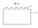
- FIG. 1A and 1B are schematic diagrams illustrating the improvement of the diffraction efficiency of the transmission type emission diffraction grating by the thin film coating.
- FIG. 1A is a schematic view of a cross section of a plastic light guide plate.
- the light guide plate 100 is made of a plastic material, and an emission diffraction grating 102 is formed on the surface as an uneven pattern.
- plastic molding techniques such as injection molding, these are formed of the same material as integral molding.
- the aspect ratio (height / width) of the uneven pattern of the exit diffraction grating is approximately 1 or less.
- the amount of phase modulation of the exit diffraction grating with respect to the incident light is governed by the difference between the refractive index of the plastic material in the convex portion and the refractive index of the air in the concave portion.
- FIG. 1B is a model diagram in the case where the coating layer 103 is formed of a dielectric film on the surface of the exit diffraction grating 102 by a sputtering method or the like.
- An uneven pattern of the dielectric material is formed on the surface, reflecting the unevenness of the original diffraction grating pattern.
- the amount of phase modulation becomes large so as to reflect the difference in the refractive index between the dielectric material and air.
- the aspect ratio of the uneven pattern is 1 or less, it is possible to obtain a large diffraction efficiency.
- the film thickness of the dielectric material it is necessary to determine the film thickness of the dielectric material so that a predetermined diffraction efficiency can be obtained by performing electromagnetic field analysis by the FDTD (Finite Differential Time Domain) method or the like.
- FDTD Finite Differential Time Domain
- the proven plastic molding technology such as the injection molding method
- As a method for reducing the aspect ratio of the uneven pattern it is desirable to adopt a diffraction grating with a two-dimensional mesh pattern as the exit diffraction grating 102.
- the aspect ratio of the uneven pattern transferred to the surface of the light guide plate is easily reduced to 1 or less, and the light guide plate using a proven plastic molding technique such as an injection molding method can be easily provided.
- Photonic crystals and diffraction gratings spatially perform phase modulation on incident light due to surface irregularities.
- the magnitude of phase modulation increases in proportion to the difference between the surface structure and the refractive index of air and the height of surface irregularities.
- FIG. 2 shows the wave number of the emission diffraction grating 102 in an exemplary manner.
- the phase functions of the diffraction gratings having wave numbers K1 and K2 with an azimuth angle of ⁇ 60 degrees with respect to the Y axis are shown in FIGS. 2 (a) and 2 (b), respectively, and each has a sinusoidal phase distribution. ..
- the phase modulation amount is standardized to 1.
- FIG. 2C is obtained, and it can be said that the photonic crystal described in Patent Document 1 and the like is formed on the surface of the light guide plate with a material having a high refractive index, which is similar to a pillar or the like.
- the maximum value of the phase modulation amount of K1 + K2 is 2, and when this is approximated by an isolated cylinder or the like, it is compared with the single sinusoidal diffraction grating shown in FIGS. 2 (a) and 2 (b). It can be seen that twice the height (aspect ratio) is required.
- FIG. 3 is a perspective view of an example in which the exit diffraction grating 102 is a mesh-shaped exit diffraction grating.
- the exit diffraction grating 102 is a mesh-shaped exit diffraction grating.
- it since it does not have a sinusoidal structure, it has a higher-order wavenumber component when it is Fourier transformed, but when it is used as a light guide plate, it has a second-order or higher-order wavenumber component by appropriately selecting the period.
- the mesh-shaped diffraction grating is made by superimposing a rectangular diffraction grating of ⁇ 60 degrees, and has no wavenumber component other than the directions of the fundamental waves K1 and K2 as compared with a cylinder or the like, so that the diffraction efficiency is high. Can be high.
- the description will proceed with a coordinate system in which the optical axis direction is the Z axis and the surface of the light guide plate is the XY plane. Further, when the user's pupil is approximated to a circle, the emission position in the light guide plate visually recognized by the user according to the pixel position is also a circle. Hereinafter, this will be referred to as an emission circle.
- FIG. 4 is a schematic diagram for explaining the exit circle.
- the projector 300 which is a light source for forming an image
- the user's pupil 400 are arranged on opposite sides of the light guide plate 100.
- the arrow in FIG. 4 represents a light ray in the xx plane.
- the incident diffraction grating 101 does not have a wave vector component in the x direction.
- the ray 301 in the center of the display image which corresponds to the center of the field of view, travels straight in the xz plane and is delivered to the user's pupil 400, as shown in the figure.
- the diffraction in the y direction which is the action of the light guide plate 100, is not explicitly expressed, it is diffracted at least once by the incident diffraction grating 101 and the outgoing diffraction grating 102.
- the rays 302 around the display image corresponding to the periphery of the visual field travel in the right direction in the figure when there is no diffraction in the x direction.
- the exit circle 303 is a virtual circle on the exit diffraction grating 102 in which the user's pupil 400 is translated in the direction of the visible light beam.
- the emission diffraction grating 102 needs to have a diffraction action in the x direction.
- FIG. 5 shows the intensity distribution of the light rays propagating inside the light guide plate calculated by using the simulation method described later. Note that the intensity distribution is shown here on the in-plane xy plane including the diffraction grating of the light guide plate.
- the incident diffraction grating 101 is arranged on the upper side, and the pupil corresponding to the user's eye is arranged below the incident diffraction grating 101.
- FIG. 5A shows the light intensity distribution to the center of the projected image when the pixel position is in the center of the projected image.
- the emission circle in the figure indicates the region where the light ray reaching the pupil was last diffracted on the emission diffraction grating 102.
- a region having high brightness on a straight line from the incident diffraction grating 101 in the y direction indicates a main ray group (hereinafter, main ray group) that is diffracted by the incident diffraction grating 101 and propagates inside the light guide plate.
- main ray group main ray group
- the low-luminance ray group spreading around the main ray group is a ray group that is diffracted by the emission diffraction grating 102 and whose traveling direction is deflected in the xy plane.
- the projected light beam is in the z-axis direction, it can be seen that the exit circle and the pupil coincide with each other in the xy plane. Therefore, it is a part of the strong main ray group that reaches the pupil and is recognized as an image.
- FIG. 5B shows the light intensity distribution around the image in the case of the pixel position in the upper right corner of the projected image.
- the main ray group travels in the lower right direction from the incident diffraction grating 101.
- the position of the pupil is constant, but since the emission circle is the emission position of the ray group traveling to the upper right toward the pupil, it shifts to the lower left with respect to the pupil in the xy plane.
- the emission circle is located away from the main ray group, the brightness of the ray group that reaches the pupil and is recognized as an image is lower than that in the above case.
- the above is the main reason why the luminance unevenness occurs when the image is projected using the light guide plate 100.
- the Monte Carlo ray tracing method can faithfully reproduce reflections and refractions, it is essential to develop a suitable model for diffraction.
- a diffraction model corresponding to the wavelength range (about 400-700 nm) over the entire visible light range and the incident angle range corresponding to the viewing angle (about 40 °) of the projected image is indispensable and is commercially available.
- the amount of calculation is enormous in the simulator.
- an algorithm that reduces the amount of calculation to 1/1000 or less by an algorithm that stops the calculation of the light rays that waveguide to the invisible region in advance is used. ..
- the calculation result by the FDTD method is tabulated and referred to in advance.
- FIG. 6 shows the configuration of the image display element of the embodiment.
- the image display element 10 is composed of two light guide plates 100a and 100b, and an incident diffraction grating 101 and an outgoing diffraction grating 102 are formed, respectively.
- the incident diffraction grating 101 is a linear surface uneven type diffraction grating.
- a blazed diffraction grating (blazed grating) having high diffraction efficiency is exemplified, but the type is not particularly limited.
- the pattern period of each of the outgoing diffraction gratings 102 is the same as that of the incident diffraction grating 101.
- a coating layer 103 is formed on the surface of the exit diffraction grating 102, respectively.
- the light guide plates 100a and 100b have different pattern periods P1 and P2, and have different wavelength ranges.
- P1 ⁇ P2 the light guide plate 100a mainly functions for displaying the short wavelength side of the wavelength range of the color image
- the light guide plate 100b mainly functions for displaying the long wavelength side.
- P1 is, for example, 360 nm
- P2 is, for example, 460 nm.
- the number of the light guide plates 100 is arbitrary, and may be one or a plurality of three or more depending on the wavelength of the light to be handled. It is desirable to change the pattern period of each light guide plate according to the wavelength to be handled.
- the incident diffraction grating 101 is arranged on the surface of the light guide plate 100 opposite to the incident surface of the image light.
- the exit diffraction grating 102 is formed on the same surface as the incident diffraction grating 101.
- both diffraction gratings are formed on the same surface, only one stamper is required to form the diffraction grating pattern, which is advantageous in terms of cost.
- the inventors examined the diffraction efficiency of the emission diffraction grating, considering the reflection diffraction for guiding the light in the light guide plate 100, it is better to let the user visually recognize the primary reflected diffraction light. It is known that can be increased.
- both the incident diffraction grating 101 and the exit diffraction grating 102 are arranged on the surface opposite to the incident surface of the image light as shown in FIG. 6, the user can visually recognize the primary transmitted diffraction grating, and the configuration for improving the brightness is configured. It will be important. It is also possible to form the incident diffraction grating 101 and the outgoing diffraction grating 102 on opposite surfaces.
- the shape of the exit diffraction grating 102 may be a straight stripe shape similar to that of the incident diffraction grating 101, or may be a mesh shape shown in FIG.
- the mesh shape has the effect of further increasing the diffraction efficiency, but does not exclude the shape of other diffraction gratings.
- the emission diffraction grating 102 is basically formed on only one surface of the light guide plate 100. That is, in the example of FIG. 6, the surface of the light guide plate 100 opposite to the exit diffraction grating 102 has no pattern and is basically flat. The surface opposite to the exit diffraction grating 102 is substantially not diffracted, and the light beam is ideally totally reflected. If one emission diffraction grating is dispersedly arranged on both sides of the light guide plate 100, there is a possibility that the positions of both diffraction gratings may be displaced due to thermal expansion of the light guide plate or the like.
- the video configuration emitted from the projector 300 can be visually recognized by the user's pupil 400.
- the light from the projector 300 is incident on the image display element 10 from the side opposite to the user's pupil 400.
- the projector 300 it is not necessary for the projector 300 to be physically arranged on the opposite side of the user's pupil 400, and a light ray from the projector 300 arranged at an arbitrary position is incident on an arbitrary surface of the light guide plate 100 with a mirror or the like. It should be.
- FIG. 7 shows an example of the relationship between the wave number vectors of the incident diffraction grating 101 and the exit diffraction grating 102 formed on one light guide plate 100.
- FIG. 8A is a simulation result of a perspective view of a pillar-shaped photonic crystal described in “Patent Document 1” and a projected image thereof.
- FIG. 8B is a simulation result of a perspective view of the mesh type diffraction grating of this embodiment and its projected image. The conditions other than the shape are the same.
- the mesh type diffraction grating of this example can obtain a good projection image with a pattern having a low aspect ratio.
- the w / p of the mesh type diffraction grating of this example needs to be set in the range of 0.15 or more and 0.85 or less.
- the efficiency was highest in the range of w / p of 0.3 or more and 0.7 or less, and the highest efficiency was in the range of w / p of 0.4 or more and 0.6 or less.
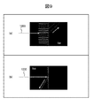
- FIG. 9A is a simulation result of the same transmission type diffraction grating as in “Patent Document 3”.
- the incident light is transmitted and diffracted and propagates inside the light guide plate (board) 100.
- the position of the incident diffraction grating 101 is formed on a surface of the light guide plate 100 close to the light source.
- the image ray 1000 is configured to be incident from the left, and the right half of the figure represents the substrate (Sub).
- the transmission type diffraction grating the maximum diffraction efficiency can be obtained under the condition that the refraction due to the blaze surface and the diffraction due to the periodic structure are phase-tuned.
- the height of the uneven pattern needs to be large, the angle of the pattern needs to be 70 to 80 degrees, and the aspect ratio obtained by dividing the height of the pattern by the cycle needs to be 10 or more. is there.
- a general plastic molding method such as injection molding, if the aspect ratio exceeds 1, problems such as deterioration of transferability occur, and the yield at the time of mass production decreases. It can be seen that the transmission type diffraction grating shown here is not suitable as the incident diffraction grating of this embodiment.
- FIG. 9B is a simulation result of a reflection type diffraction grating.
- the incident light is reflected and diffracted, that is, reflected toward the light source side and propagates inside the light guide plate (board) 100.
- the position of the incident diffraction grating 101 is formed on a surface far from the light source of the light guide plate 100.
- the image ray 1000 is similarly configured to be incident from the left, and the left half of the figure represents the substrate (Sub).
- the maximum diffraction efficiency can be obtained under the condition that the reflection by the blaze surface and the diffraction by the periodic structure are phase-tuned. As can be seen in the figure, it can be seen that this condition is satisfied by the uneven pattern having a lower aspect ratio than the transmissive type.
- the height of the uneven pattern at this time is about 250 nm, and the aspect ratio is about 0.57.
- a triangular uneven pattern having a pattern height of 374 nm could be transferred satisfactorily.
- the incident diffraction grating suitable for the light guide plate of the present embodiment adopting the plastic formation is a reflection type incident diffraction grating.
- FIGS. 10A and 10B are schematic views showing the influence of the relative inclination of the two light guide plates 100.
- the light guide plate 100 is composed of light guide plates 100a and 100b having different corresponding wavelengths, respectively.
- 300 represents a projector for image projection
- 400 represents a user's pupil
- 500 represents a projected image ray.
- the incident diffraction grating 101 is formed on a surface (right surface in the drawing) of the light guide plate 100 far from the projector 300.
- the emission diffraction grating 102 is also formed on a surface far from the projector 300 because the accuracy can be improved by forming the emission diffraction grating 102 on the same surface as the incident diffraction grating 101 for the convenience of the process.
- FIG. 10A shows a case where the projector 300 and the user's pupil 400 are arranged on the same side with respect to the light guide plate 100.
- the light guide plate 100 finally reflects the image light ray 500 and delivers it to the user's pupil 400. Therefore, if the light guide plate 100b is tilted as compared with the light guide plate 100a, the visible pixel position shifts depending on the wavelength of the projected light beam, and the image quality deteriorates. Since the resolution ability of the ray angle of a user with a visual acuity of 1.0 is 1/60 degree, the relative inclination of the two light guide plates needs to be sufficiently smaller than 1/60 degree based on this.
- FIG. 10B shows a case where the projector 300 and the user's pupil 400 are arranged on opposite sides of the light guide plate 100.
- the light guide plate 100 finally transmits the image light ray 500 and reaches the user's pupil 400. Since the angles of the incident light and the emitted light are basically the same, even if there is a relative inclination between the light guide plates 100a and 100b, the projection image does not shift due to the wavelength in principle. Therefore, when the plastic light guide plate of this embodiment is mounted on the head-mounted display, it is desirable that the projector light source is on the side opposite to the user's pupil 400 (transmissive optical configuration) with respect to the light guide plate 100.
- the relative inclination of the light guide plates 100a and 100b it is desirable to keep the relative inclination of the light guide plates 100a and 100b to about 3 degrees or less because the light angle condition that totally reflects and guides the inside of the light guide plate is actually affected.
- the light propagating through the light guide plate 100 is diffracted by the exit diffraction grating 102, and the diffraction efficiency when the light is emitted from the light guide plate 100 is calculated by the FDTD method.
- the wavelength is 550 nm
- the refractive index of the light guide plate is 1.58
- the pattern period of the diffraction grating is 460 nm
- the width of the convex portion is 150 nm
- the height of the convex portion is 70 nm.
- the reflection diffraction efficiency was 3.5% and the transmission diffraction efficiency was 2.8% under the condition of total reflection propagation inside the light guide plate.
- the aspect ratio of the uneven pattern is 0.47.
- the outgoing diffraction grating 102 is formed on the same surface as the incident diffraction grating 101 as in FIG. 10B, the light beam visually recognized by the user is transmitted and diffracted by the outgoing diffraction grating 102. Therefore, in the transmission type optical configuration shown in FIG. 10B, the brightness of the projected image visually recognized by the user is lower than that in the reflection type optical configuration of FIG. 10A.
- the thin film coating on the exit diffraction grating 102 is formed by a sputtering method, and the film thickness of the dielectric thin film is shown on the horizontal axis as a ZnS-SiO 2 (20%) thin film (refractive index 2.33).
- the vertical axis shows the transmission diffraction efficiency and the transmittance of the light guide plate.
- the light propagating through the light guide plate 100 is diffracted by the exit diffraction grating 102, and the transmission diffraction efficiency when the light is emitted from the light guide plate 100 is calculated by the FDTD method.
- the wavelength is 550 nm
- the refractive index of the light guide plate 100 is 1.58
- the pattern period of the exit diffraction grating 102 is 460 nm
- the width of the convex portion is 150 nm
- the height of the convex portion is 70 nm.
- the transmission diffraction efficiency was calculated under the condition that the light guide plate 100 was totally reflected and propagated inside the light guide plate 100.
- the transmission diffraction efficiency is improved and it is possible to provide high-luminance image information.
- the transmission diffraction efficiency is 7.3%, which is 2.5 times or more the efficiency of 2.8% when no coating is applied. It is possible to improve.
- the transmission diffraction efficiency is 9.3%, and it is possible to improve the efficiency by 3 times or more as compared with 2.8% when no coating is applied.
- the improvement in diffraction efficiency is also reflected in the reflection diffraction efficiency, and when a film thickness of about 20 nm or more is formed, it can exceed the reflection diffraction efficiency when no coating is applied. Therefore, even if the exit diffraction grating 102 is formed on the same surface as the incident diffraction grating 101, a large brightness can be obtained.
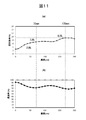
- FIG. 11B shows the calculation result of the transmittance of the light guide plate, which corresponds to the brightness when the user visually recognizes the outside world.
- the transmittance of the light guide plate is reduced to about 72% compared to about 91% when the dielectric thin film is not formed. ..
- This means that, for example, when the user uses the head-mounted display of this embodiment outdoors, the image of strong external light is dimmed to about 80% ( 72% / 91%) and the brightness of the projected image is reduced to about 80%. There is an effect of improving the visibility of the projected image by improving it 2.5 times (7.3% / 2.8%).
- the film thickness of the dielectric film is 170 nm
- the brightness of the projected image looks brighter than that of the outside world.
- the transmittance is 68 to 80% in the range of the film thickness of 70 nm or more and 170 nm or less, and the relative brightness of the projected image with respect to the outside world is improved in consideration of the effect of improving the diffraction efficiency. It is possible to do.
- the density and internal stress of a dielectric thin film formed by a sputtering method or the like changes depending on the film forming conditions such as equipment, target, degree of vacuum, and RF (radio frequency) power.
- the refractive index of the dielectric thin film formed by the inventors was identified using the measurement results of the reflectance and the transmittance by a spectrophotometer.
- the refractive index may differ by about ⁇ 5%, so it should be added.
- a dielectric material such as ZnS, AlN, SiNx, SiO, AlON, Al 2 O 3 , etc. may be used in addition to ZnS-SiO 2 (20%) shown here. it can.
- a coating layer such as a dielectric material is formed on the surface of the emission diffraction grating by a sputtering method or the like to generate emission light. It is possible to increase the diffraction efficiency to 4% or more. If a mesh-type emission diffraction grating is used, the light guide plate can be made of plastic by an injection molding method or the like, and a safe, lightweight, and high-brightness light guide plate can be realized.
- the light propagating through the light guide plate 100 is diffracted by the exit diffraction grating 102, the transmission diffraction efficiency when the light is emitted from the light guide plate 100 is calculated by the FDTD method, and the incident angle dependence of the transmission diffraction efficiency is tabulated. Using this, ray tracing was performed to obtain an image that the user could see.
- the wavelength is 635 nm
- the refractive index of the light guide plate is 1.58
- the pattern period of the diffraction grating is 460 nm
- the width of the convex portion is 150 nm
- the height of the convex portion is 90 nm.
- the thickness of the light guide plate 100 is 1 mm
- the diameter of the image light beam incident on the incident diffraction grating 101 is 4 mm
- the distance between the incident diffraction grating 101 and the exit diffraction grating 102 is 5 mm
- the user's pupil 400 from the light guide plate 100 The distance to the grating was 25 mm
- the diameter of the user's pupil 400 was 3 mm.
- FIG. 12 is an example of the object model used in the calculation. It is said that an emission diffraction grating 102 having a concavo-convex pattern is formed on the surface of the plastic light guide plate 100, and a coating layer 103 of a dielectric thin film is formed on the emission diffraction grating 102 with a constant film thickness.
- the uneven pattern has a cross-sectional shape close to a trapezoid with an inclination angle, but here, in order to simplify the calculation model, an ideal rectangular diffraction grating is assumed as the cross-sectional shape.
- As a dielectric material it is the result of ZnS-SiO 2 (20%).
- the portion 1200 shown in black in the figure indicates an air layer.
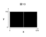
- FIG. 13 is an example of the calculated visual image.
- the display pixels are 1280 x 720 pixels, and here, the horizontal direction is the X direction and the vertical direction is the Y direction.
- the wave vector of the incident diffraction grating is in the Y direction.
- the incident angle of the image ray and the propagation angle in the light guide plate change depending on the pixel position in the Y direction of the displayed image.
- the material of the coating layer 103 was ZnS-SiO 2 (20%).
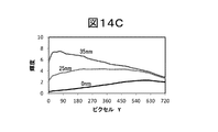
- FIG. 14A shows the angle of the light beam propagating inside the light guide plate 100, that is, the angle of incidence on the exit diffraction grating 102. It can be seen that the incident angle decreases as the pixel position increases.
- FIG. 14B is a calculation result of the transmission diffraction efficiency.
- the case where the film thickness of the coating layer 103 is 0, 25, and 35 nm is shown.
- the coating layer 103 is not formed (thickness 0 nm)
- the transmission diffraction efficiency increases as the pixel position increases.
- a dielectric thin film for example, when it is formed at 35 nm, it can be seen that the transmission diffraction efficiency can be reduced as the pixel position increases.
- 25 nm is formed, the transmission diffraction efficiency does not change relatively with the increase in the pixel position.
- FIG. 14C is a calculation result of the brightness visually recognized by the user.
- the dielectric thin film is not formed (thickness 0 nm)
- the increase in brightness is remarkable as the pixel position increases.
- the dielectric film thickness is 35 nm
- the brightness at the central portion is high, but the decrease in brightness is remarkable as the pixel position increases.
- the dielectric film thickness is 25 nm
- the brightness distribution of the image visually recognized by the user can be controlled by forming a dielectric thin film on the surface of the emission diffraction grating.
- the dielectric film thickness is 25 nm, the brightness distribution can be made flat.
- a dielectric material such as ZnS, AlN, SiNx, SiO, AlON, Al 2 O 3 , etc. can be used, and 2 such as ZnS-SiO 2 (20%). It is also possible to use a mixed material of more than one kind of dielectric.
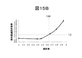
- FIG. 15A is a simulation result showing the range of the refractive index of the dielectric material suitable for this embodiment.
- the vertical axis is the transmission diffraction efficiency involved in improving the brightness in the center of the projected image, which is standardized with the case where the coating layer 103 is not present as 1.
- the transmission diffraction efficiency increases and the brightness of the visible image is improved.
- FIG. 15B is an enlargement of a part of FIG. 15A. If the diffraction efficiency is 1.2 times due to the effect of the dielectric film of this embodiment, the power consumption of the light source is reduced by 20% when the user visually recognizes an image having the same brightness as compared with the case where there is no dielectric film. It will be possible. Assuming that this condition is a condition in which the effect of this embodiment becomes apparent, it can be seen that the refractive index of the dielectric material should be 1.64 or more.
- a dielectric material such as ZnS, AlN, SiNx, SiO, AlON, Al 2 O 3 , etc. can be used, and 2 such as ZnS-SiO 2 (20%). It is also possible to use a mixed material of more than one kind of dielectric. Diamond has the highest refractive index (2.42) as a known dielectric material, and as shown in FIG. 15A, the upper limit of the refractive index of the dielectric thin film suitable for this embodiment is 2.42.
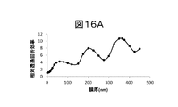
- FIG. 16A is a simulation result showing the film thickness range of the dielectric material suitable for this embodiment.
- the dielectric material was ZnS (refractive index 2.355).
- the vertical axis is the standardized transmission diffraction efficiency involved in improving the brightness in the center of the projected image.
- the film thickness is about 70 nm or more
- the diffraction efficiency is about 3 times or more that when there is no film.
- FIG. 16B shows the film thickness dependence of the reflectance of a dielectric thin film formed on a flat substrate, that is, a so-called optical thin film coating.
- the refractive index of the substrate was set to 1.58 in the same manner as above, ZnS was selected as the dielectric material, and the relationship between the film thickness and the reflectance was calculated.
- the reflectance changes periodically with respect to the film thickness.
- the film thickness dependence of such a dielectric thin film is well known.
- the dielectric thin film on the diffraction grating is characterized in that it contains a monotonous increase component of diffraction efficiency with respect to an increase in film thickness in addition to periodicity.
- FIG. 16C is an enlargement of FIG. 16A.
- the film thickness of the dielectric material may be 10 nm or more.
- the dielectric thin film formed on the diffraction grating is formed along the uneven shape of the original diffraction grating, and the film thickness is uneven.
- the uneven shape of the dielectric thin film surface is gradually lost and approaches flat, depending on the film formation process such as the sputtering method or the vacuum deposition method. It is also known that it is fixed. Therefore, the upper limit of the film thickness at which the effect of this example appears is approximately 1000 nm.
- Example 3 a dielectric thin film suitable for the incident diffraction grating 101 will be examined.
- the incident diffraction grating 101 described below is a reflection type diffraction grating, and includes a multilayer coating layer on the reflection type diffraction grating.
- the multilayer coating layer has a periodic structure in which the first dielectric thin film and the second dielectric thin film are alternately formed, so that excellent wavelength dependence can be obtained.
- FIG. 17 is a simulation result of the range of the display image for each light guide plate.
- a case of a light guide plate composed of two light guide plates 100a (for short wavelength) and 100b (for long wavelength) is shown.
- the pitch of the input / output diffraction grating is 360 nm for the light guide plate 100a (for short wavelength), 460 nm for the light guide plate 100b (for long wavelength), the diagonal viewing angle of the display image is 35 degrees, and the aspect ratio is 16: 9.
- the display range indicated by the white part in the figure
- the light guide plate 100a is a part of the B image (blue display image) and the G image (green display image).
- the light guide plate 100b contributes to the display of a part of the G image (green display image) and the R image (red display image).
- the incident diffraction grating 101a provided on the light guide plate 100a in FIG. 6 reflects and diffracts the B wavelength (blue wavelength) with a large diffraction efficiency, and reflects and diffracts the G wavelength (green wavelength) with a smaller diffraction efficiency. It can be seen that it is desirable to almost transmit the wavelength (red wavelength). This means that strong wavelength dependence is required for diffraction efficiency.
- a dichroic film is known as an optical element that reflects such a short wavelength light ray and transmits a long wavelength light ray, and can be realized by a dielectric multilayer thin film formed on a transparent substrate.
- the dielectric thin film formed on the surface uneven diffraction grating exhibits a film thickness dependence different from that of a general optical thin film.
- the conditions of a dielectric thin film suitable for forming on an incident diffraction grating are shown.
- the main performance indicators of the light guide plate 100a (for short wavelengths) are the reflection primary diffraction efficiency and the transmittance.
- FIG. 18 shows another configuration of the image display element of this embodiment.
- the image display element 10 is composed of two light guide plates 100a and 100b, and an incident diffraction grating 101a and 101b and an outgoing diffraction grating 102a and 102b are formed, respectively.
- the incident diffraction gratings 101a and 101b are linear or lattice-shaped surface-concavo-convex diffraction gratings.
- the pattern period of the outgoing diffraction gratings 102a and 102b is the same as that of the incident diffraction gratings 101a and 101b, respectively.
- Coating layers 103a and 103b are formed on the surfaces of the exit diffraction gratings 102a and 102b, respectively.
- the light guide plates 100a and 100b have different pattern periods P1 and P2, and the corresponding wavelength ranges are different.
- P1 ⁇ P2 the light guide plate 100a mainly displays the short wavelength side of the wavelength range of the color image.
- the light guide plate 100b mainly functions for displaying on the long wavelength side.
- the structural difference from FIG. 6 is that the coating layers 104a and 104b are also formed on the incident diffraction gratings 101a and 101b by the dielectric film.
- FIG. 19 is a schematic diagram showing the cross-sectional shape of the reflection type incident diffraction grating 101.
- a reflection type incident diffraction grating is suitable for the light guide plate of this embodiment.
- a stepped concave-convex diffraction grating having a cross-sectional shape of 5 levels in height is illustrated.
- the pitch of the diffraction grating is P, and the wavelength of the light beam is ⁇ .
- the incident light 1901 incident from the lower side of the paper surface is first reflected and first diffracted in the lower right direction of the paper surface to become diffracted light 1902.
- This is a well-known basic principle of diffraction. In order to consider a dielectric coating suitable for the incident diffraction grating 101 of this embodiment, this basic principle is extended in the height z direction of the diffraction grating.
- FIG. 20 is a schematic diagram for considering a dielectric coating suitable for this embodiment.
- the pitch P of the incident diffraction grating 101 was determined corresponding to the wavelength ⁇ to be selected.
- the broken line in the figure is a periodic extension of the shape of the height-modulated diffraction grating.
- H is defined as the periodic height of the incident diffraction grating 101.
- diffracted light having the same angle is generated from the virtual diffraction grating having a broken line shape, and the periodic height H of the diffraction grating corresponds to the wavelength ⁇ with respect to the diffracted light.
- Suitable dielectric coatings for the incident diffraction grating 101 of this embodiment include at least two types of materials having a high refractive index (refractive index n1, film thickness d1) and a material having a low refractive index (refractive index n2, film thickness d2). It is used, and this is alternately laminated on the diffraction grating. At this time, a dielectric layer reflecting the surface uneven shape of the diffraction grating is formed on the upper side of the surface of the diffraction grating in the z direction.
- a suitable condition for this embodiment is d1 + d2 ⁇ H.
- FIG. 21 summarizes the relationship between the periodic height H of the diffraction grating and the height shape of one period.
- the periodic height H is defined as the value shown in the figure in a stepped diffraction grating having a height of 5, 4, 3, and 2 levels, a blaze type diffraction grating, and a diffraction grating having a general shape.
- H (N / N-1) h Will be.
- the period height H is the height extended to one period from the inclination of the main blaze surface.
- the so-called blaze angle is ⁇ B.
- H ⁇ (p 1 + p 2 ) / p 1 ⁇ h Will be.
- H P ⁇ tan ⁇ B , where P is the diffraction grating period by determining the blaze angle ⁇ B from the average slope. Will be.
- FIG. 22A is a simulation model showing the cross-sectional shape of the incident diffraction grating 101 of this embodiment.
- the auxiliary line in the figure represents the equiphase line 610 in the height direction shown above, and by shifting to the right by one cycle in the X direction in the figure due to the periodicity of the diffraction grating, it becomes the equiphase line 610.
- the distance of the uneven pattern in the Z direction increases at equal intervals by the periodic height H, such as H, 2H, and 3H.
- the height h of the diffraction grating is 100 nm, and the period is 360 nm.
- the refractive index of the plastic substrate constituting the incident diffraction grating 101 is 1.58 when the substrate is polycarbonate, and the periodic height H is 150 nm.
- the black part in the figure is the air layer (Air).
- FIG. 22B is a simulation model showing the cross-sectional shape of the incident diffraction grating 101 of this embodiment.
- a first dielectric film 221 with a high refractive index (refractive index n1, thickness d1) and a second dielectric film 222 with a low refractive index (refractive index n2, thickness d2) are placed on the incident diffraction grating 101.
- n1> n2, d1 + d2 H.
- the diffraction grating group formed by the dielectric layer in the z direction can be formed so as to be aligned on the equiphase planes 610a, 610b, 610c and the like.
- the diffracted light generated from these diffraction grating groups is phase-matched, and a large diffraction efficiency can be obtained.
- the pitch of the diffraction grating is determined according to the selected wavelength (blue light in this case).
- FIG. 23A is a simulation model in which the Al film 231 is laminated by 100 nm on the incident diffraction grating 101 having a height of 3 levels as a reference.
- FIG. 23B is a simulation model in which the Al film 231 is laminated by 100 nm on the blaze type incident diffraction grating 101 as a reference.
- FIG. 24A is a simulation result of the reflection primary diffraction efficiency and the transmittance of the incident diffraction grating in which a five-layer dielectric thin film is formed on the three-level height diffraction grating shown in FIG. 22B.
- the incident angle is 0 degrees, which corresponds to the center of the displayed image.
- the primary reflection efficiency is large in the B (blue, 460 nm) wavelength band to the G (green, 530 nm) wavelength band, zero in the R (red, 640 nm) wavelength band, and the maximum is the B wavelength. It is about 80% in the obi.
- the transmittance is about 20% in the B wavelength band and 80% or more in the R wavelength band, which can provide suitable wavelength dependence for the short wavelength light guide plate 100a described with reference to FIG.
- FIG. 24B is a simulation result of an incident diffraction grating in which an Al thin film is formed on the diffraction grating with a height of 3 levels shown in FIG. 23A.
- the diffraction efficiency in the B wavelength band is about 50%, and the transmittance is almost zero in the entire wavelength range.
- FIG. 24C is a simulation result of an incident diffraction grating in which an Al thin film is formed on the blaze type diffraction grating shown in FIG. 23B.
- the diffraction efficiency in the B wavelength band is about 50%, and the transmittance is almost zero in the entire wavelength range.
- the incident diffraction grating on which the dielectric film is laminated can achieve both higher diffraction efficiency and higher transmittance in the long wavelength band than the blaze type diffraction grating on which the Al reflective film is formed. It turned out that there was. This is a performance characteristic suitable for an incident diffraction grating of a light guide plate.
- FIG. 25 is a simulation result when the total thickness (d1 + d2) deviates from the periodic height H with respect to the dielectric thin film of FIG. 22B.
- the axis is (d1 + d2) / H, and the case where this value is 1 is the condition for phase matching.
- the diffraction efficiency when the Al reflective film was formed on the incident diffraction grating was about 50%.
- the periodic height H of the diffraction grating corresponds to the phase 2 ⁇ (360 degrees) of the light beam. Therefore, it can be said that the condition range shown here has a phase difference of ⁇ 110, which is a reasonable result even in light of the wave superposition condition.
- the light guide plate 100a for short wavelengths has been described, but the same applies to the light guide plate 100b for long wavelengths by determining the pitch of the diffraction grating corresponding to the wavelength (for example, red light) for selecting the pitch. The effect can be obtained.
- FIG. 26 is a schematic diagram showing the film shape when 13 layers of the dielectric thin films of this embodiment are laminated.
- the first dielectric film 221 and the second dielectric film 222 are sequentially laminated on the incident diffraction grating 101 formed of plastic by a vacuum vapor deposition method, a sputtering method, or the like, the surface of the plastic substrate is covered with the first dielectric film 221 and the second dielectric film 222.
- a diffraction grating composed of the formed uneven pattern a certain amount of dielectric material is laminated on the side wall thereof.
- the shape of the dielectric film gradually changes between the layer on the lower side of the paper surface and the layer on the upper side of the paper surface.
- the dielectric film of this embodiment has an upper limit on its total thickness.
- the value of this upper limit is about 10 times the height of the uneven pattern, and is about 1000 nm as described above.
- FIG. 27 is a diagram showing an example of an image display element in which the coating layer 104 is provided on the incident diffraction grating 101 and not provided on the exit diffraction grating 102.
- the coating layer 104 is provided on the incident diffraction grating 101 and not provided on the exit diffraction grating 102.
- the incident diffraction grating 101 the effect of the dielectric film can be obtained.
- FIG. 28 is a model diagram of a method of integrally molding a diffraction grating on both sides of the light guide plate shown in FIG. 1 by a plastic molding technique.
- Conventionally used light guide plates such as nanoimprint method and etching are surface processing technologies based on semiconductor processing technology.
- the plastic molding technology such as the injection molding method is a three-dimensional molding technology in which a resin is introduced into the mold and hardened, it is easy to form diffraction gratings on both sides of the light guide plate.
- the stamper 700 having the surface shape of the diffraction grating to be formed inverted on the surface is fixed to the fixing portion 710 of the mold.
- the molten resin 740 is injected from the resin flow path 730, and the resin 740 is formed by applying pressure by moving the mold movable portion 720 to the right in the drawing. It is possible to form a desired light guide plate through a cooling process while forming a shape that follows the shape of the cavity 750.
- This method is general, and a light guide plate in which a diffraction grating is formed as an uneven shape can be made of plastic.
- FIG. 29 is a schematic diagram showing the configuration of the image display device of this embodiment.
- plastic is used as the material of the light guide plate 100.
- a reflection type diffraction grating capable of having a low aspect ratio is used as the incident diffraction grating 101. Since the reflection type incident diffraction grating reflects light inside the light guide plate 100, the incident diffraction grating 101 is placed on the surface (second surface) opposite to the incident surface (first surface) of the image light beam of the light guide plate 100. Be placed.
- the light guide plate 100 has a configuration in which the user visually recognizes the light in which the primary reflection diffraction is dominant, so that the visible brightness can be increased at a low aspect ratio. Therefore, when the diffraction efficiency is emphasized.
- the exit diffraction grating is preferably arranged on the first surface so that the first-order reflected diffracted light is emitted to the second surface.
- the exit diffraction grating 102 is also formed on the same surface (second surface), and the primary transmitted diffracted light is emitted to the second surface. I have to.
- the diffraction efficiency is improved by forming a dielectric film on the diffraction grating.
- the coating layer 103 is formed on the exit diffraction grating 102 as in FIG. It is also possible to form the coating layer 104 on the incident diffraction grating 101 as shown in FIG. 27. Alternatively, as shown in FIG.
- the coating layers 103 and 104 can be formed on both the incident diffraction grating 101 and the outgoing diffraction grating 102.
- the multilayer dielectric film described with reference to FIG. 22B is excellent in wavelength selectivity and effective.
- the lattice-shaped diffraction grating shown in FIG. 3 can obtain high diffraction efficiency with a low aspect ratio.
- the configuration of the image display element is not limited to the above, and various configurations of the incident diffraction grating and the exit diffraction grating can be considered. Even in that case, the diffraction efficiency is improved and the brightness is improved by controlling the characteristics of the film to be formed according to the reflection diffraction efficiency and the transmission diffraction efficiency required for each of the incident diffraction grating and the outgoing diffraction grating. Can be done.
- the light having the image information emitted from the projector 300 in the figure is delivered to the user's pupil 400 by the action of the light guide plates 100a and 100b, and realizes augmented reality.
- the pitch and depth of the diffraction grating formed are optimized according to each color.
- the image display device of this embodiment includes an image display element 10, a projector 300, and a display image control unit 2901.
- the image forming method include an image forming apparatus composed of a reflective or transmissive spatial light modulator, a light source and a lens, and an image forming apparatus using an organic and inorganic EL (Electro Luminescence) element array and a lens.
- a widely known image forming apparatus such as an image forming apparatus using a light emitting diode array and a lens and an image forming apparatus combining a light source and a semiconductor MEMS mirror array and a lens can be used.
- an LED or laser light source in which the tip of the optical fiber is resonated by MEMS technology, PZT, or the like.
- MEMS technology PZT
- the most common is an image forming apparatus consisting of a reflective or transmissive spatial light modulator, a light source, and a lens.
- the spatial light modulator include a transmissive or reflective liquid crystal display device such as LCOS (Liquid Crystal On Silicon) and a digital micromirror device (DMD), and the white light source is RGB-separated as the light source. It is also possible to use an LED or a laser corresponding to each color.
- the reflective spatial light modulator reflects a part of the light from the liquid crystal display device and the light source and guides the light to the liquid crystal display device, and passes a part of the light reflected by the liquid crystal display device.
- It can be configured to consist of a polarizing beam splitter that leads to a collimating optical system using a lens.
- the light emitting element constituting the light source include a red light emitting element, a green light emitting element, a blue light emitting element, and a white light emitting element.
- the number of pixels may be determined based on the specifications required for the image display device, and as specific values of the number of pixels, in addition to the 1280x720 shown above, 320 ⁇ 240, 432 ⁇ 240, 640 ⁇ 480. 1024 ⁇ 768 and 1920 ⁇ 1080 can be exemplified.
- the light rays including the image information emitted from the projector 300 are positioned so as to be irradiated to the incident diffraction gratings of the light guide plates 100a and 100b, and are integrated with the image display element 10. Is formed.
- the display image control unit (not shown) controls the operation of the projector 300 and fulfills a function of appropriately providing image information to the user's pupil 400.
- the light guide plate image display element having a surface uneven surface type diffraction grating
- a mesh type diffraction grating is used as the emission diffraction grating, and a material having the same refractive index as the waveguide by an injection molding method or the like is used.
- the light guide plate can be made into a plastic, and a safe and lightweight light guide plate can be realized. That is, by using a mesh type diffraction grating, it is possible to create a light guide plate having good performance with surface irregularities of an aspect ratio of 1 or less by the injection molding method, and the safety and weight reduction are realized by making the light guide plate plastic. We were able to.
- the image display device of this embodiment also includes a touch sensor, a temperature sensor, an acceleration sensor, etc. for acquiring information on the user and the outside world. It is possible to equip various sensors and an eye tracking mechanism for measuring the movement of the user's eyes.
Landscapes
- Physics & Mathematics (AREA)
- General Physics & Mathematics (AREA)
- Optics & Photonics (AREA)
- Engineering & Computer Science (AREA)
- Manufacturing & Machinery (AREA)
- Multimedia (AREA)
- Signal Processing (AREA)
- Diffracting Gratings Or Hologram Optical Elements (AREA)
Priority Applications (2)
| Application Number | Priority Date | Filing Date | Title |
|---|---|---|---|
| CN202080089119.4A CN114846386B (zh) | 2020-01-10 | 2020-10-08 | 图像显示元件以及图像显示装置 |
| US17/782,692 US20230010994A1 (en) | 2020-01-10 | 2020-10-08 | Image display element and device |
Applications Claiming Priority (2)
| Application Number | Priority Date | Filing Date | Title |
|---|---|---|---|
| JP2020002825A JP7341907B2 (ja) | 2020-01-10 | 2020-01-10 | 画像表示素子および装置 |
| JP2020-002825 | 2020-01-10 |
Publications (1)
| Publication Number | Publication Date |
|---|---|
| WO2021140717A1 true WO2021140717A1 (ja) | 2021-07-15 |
Family
ID=76788158
Family Applications (1)
| Application Number | Title | Priority Date | Filing Date |
|---|---|---|---|
| PCT/JP2020/038161 Ceased WO2021140717A1 (ja) | 2020-01-10 | 2020-10-08 | 画像表示素子および装置 |
Country Status (5)
| Country | Link |
|---|---|
| US (1) | US20230010994A1 (https=) |
| JP (1) | JP7341907B2 (https=) |
| CN (1) | CN114846386B (https=) |
| TW (1) | TWI753617B (https=) |
| WO (1) | WO2021140717A1 (https=) |
Families Citing this family (5)
| Publication number | Priority date | Publication date | Assignee | Title |
|---|---|---|---|---|
| JP7465826B2 (ja) * | 2021-02-02 | 2024-04-11 | 株式会社日立エルジーデータストレージ | 導光板、導光板モジュールおよび画像表示装置 |
| GB202103391D0 (en) * | 2021-03-11 | 2021-04-28 | Opsec Security Ltd | Security device |
| CN117836676A (zh) * | 2021-08-20 | 2024-04-05 | 谷歌有限责任公司 | 使用低折射率介质的单波导红绿蓝(rgb)架构 |
| FI20245457A1 (en) * | 2024-04-12 | 2025-10-13 | Dispelix Oy | Diffraction grating |
| TWI884089B (zh) * | 2024-09-30 | 2025-05-11 | 友達光電股份有限公司 | 具有低折射率與大視野之光學模組及增強實境顯示器 |
Citations (7)
| Publication number | Priority date | Publication date | Assignee | Title |
|---|---|---|---|---|
| JPH10133008A (ja) * | 1996-11-01 | 1998-05-22 | Japan Aviation Electron Ind Ltd | 多層膜回折格子およびその製造方法 |
| US20050112510A1 (en) * | 2003-09-10 | 2005-05-26 | Asml Netherlands B.V. | Optical element, lithographic apparatus, method for manufacturing and/or protecting an optical element, device manufacturing method and device manufactured thereby |
| US20100277803A1 (en) * | 2006-12-14 | 2010-11-04 | Nokia Corporation | Display Device Having Two Operating Modes |
| US20150293357A1 (en) * | 2012-10-18 | 2015-10-15 | Lg Electronics Inc. | Optical device |
| WO2016162593A1 (en) * | 2015-04-07 | 2016-10-13 | Nokia Technologies Oy | Diffraction grating and method of manufacture |
| JP2017156388A (ja) * | 2016-02-29 | 2017-09-07 | セイコーエプソン株式会社 | 光束径拡大素子及び画像表示装置 |
| US20170307886A1 (en) * | 2016-04-25 | 2017-10-26 | Petri Antero Stenberg | Refractive coating for diffractive optical elements |
Family Cites Families (21)
| Publication number | Priority date | Publication date | Assignee | Title |
|---|---|---|---|---|
| JPH0588151A (ja) * | 1991-09-27 | 1993-04-09 | Matsushita Electric Ind Co Ltd | 液晶パネルとその製造方法および液晶投写型テレビ |
| JPH0815514A (ja) * | 1994-06-24 | 1996-01-19 | Canon Inc | 反射型回折格子 |
| US5485318A (en) * | 1994-10-03 | 1996-01-16 | Motorola, Inc. | Dual image manifestation apparatus with integrated electro-optical package |
| JP2005115152A (ja) * | 2003-10-09 | 2005-04-28 | Sankyo Seiki Mfg Co Ltd | レンズ、および光ヘッド装置 |
| FR2864252B1 (fr) | 2003-12-23 | 2006-04-07 | Jobin Yvon Sas | Reseau de diffraction a empilements multicouches alternes et son procede de fabrication et dispositifs spectroscopiques comportant ces reseaux |
| CN101253425B (zh) * | 2005-08-29 | 2012-06-20 | 松下电器产业株式会社 | 衍射光学元件及制造方法、使用衍射光学元件的摄像装置 |
| WO2007036182A1 (de) * | 2005-09-30 | 2007-04-05 | Fraunhofer-Gesellschaft zur Förderung der angewandten Forschung e.V. | Mikrooptisches beugungsgitter sowie verfahren zur herstellung |
| US8441728B2 (en) * | 2008-12-26 | 2013-05-14 | Panasonic Corporation | Diffractive lens and image pickup device using the same |
| CN102236118B (zh) * | 2010-05-07 | 2013-10-16 | 同济大学 | 一种平面结构闪耀光栅 |
| US8773599B2 (en) | 2011-10-24 | 2014-07-08 | Google Inc. | Near-to-eye display with diffraction grating that bends and focuses light |
| FI125270B (en) * | 2012-09-20 | 2015-08-14 | Teknologian Tutkimuskeskus Vtt Oy | Optical device with diffractive grating |
| CN105765421B (zh) * | 2013-10-29 | 2019-07-09 | 瑞士Csem电子显微技术研发中心 | 光栅耦合结构 |
| JP2016048315A (ja) * | 2014-08-27 | 2016-04-07 | Hoya株式会社 | 発色構造体及び外装部品 |
| AU2016245280A1 (en) * | 2015-04-08 | 2017-10-19 | Dispelix Oy | Optical see-through display element and device utilizing such element |
| US10038840B2 (en) * | 2015-07-30 | 2018-07-31 | Microsoft Technology Licensing, Llc | Diffractive optical element using crossed grating for pupil expansion |
| US10073278B2 (en) * | 2015-08-27 | 2018-09-11 | Microsoft Technology Licensing, Llc | Diffractive optical element using polarization rotation grating for in-coupling |
| US10025093B2 (en) * | 2016-04-13 | 2018-07-17 | Microsoft Technology Licensing, Llc | Waveguide-based displays with exit pupil expander |
| JP6410906B1 (ja) * | 2017-09-26 | 2018-10-24 | デクセリアルズ株式会社 | 偏光素子及び光学機器 |
| WO2019089639A1 (en) * | 2017-10-30 | 2019-05-09 | Facebook Technologies, Llc | H2-assisted slanted etching of high refractive index material |
| US10845596B2 (en) * | 2018-01-23 | 2020-11-24 | Facebook Technologies, Llc | Slanted surface relief grating for rainbow reduction in waveguide display |
| JP7096084B2 (ja) | 2018-07-02 | 2022-07-05 | 株式会社日立エルジーデータストレージ | 導光板、導光板モジュール、画像表示装置および導光板の製造方法 |
-
2020
- 2020-01-10 JP JP2020002825A patent/JP7341907B2/ja active Active
- 2020-10-08 US US17/782,692 patent/US20230010994A1/en not_active Abandoned
- 2020-10-08 WO PCT/JP2020/038161 patent/WO2021140717A1/ja not_active Ceased
- 2020-10-08 CN CN202080089119.4A patent/CN114846386B/zh not_active Expired - Fee Related
- 2020-10-20 TW TW109136214A patent/TWI753617B/zh not_active IP Right Cessation
Patent Citations (7)
| Publication number | Priority date | Publication date | Assignee | Title |
|---|---|---|---|---|
| JPH10133008A (ja) * | 1996-11-01 | 1998-05-22 | Japan Aviation Electron Ind Ltd | 多層膜回折格子およびその製造方法 |
| US20050112510A1 (en) * | 2003-09-10 | 2005-05-26 | Asml Netherlands B.V. | Optical element, lithographic apparatus, method for manufacturing and/or protecting an optical element, device manufacturing method and device manufactured thereby |
| US20100277803A1 (en) * | 2006-12-14 | 2010-11-04 | Nokia Corporation | Display Device Having Two Operating Modes |
| US20150293357A1 (en) * | 2012-10-18 | 2015-10-15 | Lg Electronics Inc. | Optical device |
| WO2016162593A1 (en) * | 2015-04-07 | 2016-10-13 | Nokia Technologies Oy | Diffraction grating and method of manufacture |
| JP2017156388A (ja) * | 2016-02-29 | 2017-09-07 | セイコーエプソン株式会社 | 光束径拡大素子及び画像表示装置 |
| US20170307886A1 (en) * | 2016-04-25 | 2017-10-26 | Petri Antero Stenberg | Refractive coating for diffractive optical elements |
Also Published As
| Publication number | Publication date |
|---|---|
| CN114846386B (zh) | 2024-04-02 |
| CN114846386A (zh) | 2022-08-02 |
| JP2021110838A (ja) | 2021-08-02 |
| TW202127072A (zh) | 2021-07-16 |
| US20230010994A1 (en) | 2023-01-12 |
| TWI753617B (zh) | 2022-01-21 |
| JP7341907B2 (ja) | 2023-09-11 |
Similar Documents
| Publication | Publication Date | Title |
|---|---|---|
| CN111190288B (zh) | 导光板及图像显示装置 | |
| US10459140B2 (en) | Image display device | |
| WO2020255482A1 (ja) | 導光板、その製造方法、導光板モジュール、および画像表示装置 | |
| WO2021140717A1 (ja) | 画像表示素子および装置 | |
| CN114846387B (zh) | 图像显示元件、图像显示装置以及图像显示方法 | |
| JP4655771B2 (ja) | 光学装置及び虚像表示装置 | |
| JP6893991B2 (ja) | 反射支持構造を有するマルチビューディスプレイ | |
| JP7096084B2 (ja) | 導光板、導光板モジュール、画像表示装置および導光板の製造方法 | |
| CN108885309B (zh) | 使用反射光栅岛的基于光栅的背光体 | |
| JP7465826B2 (ja) | 導光板、導光板モジュールおよび画像表示装置 | |
| HK40008152A (en) | Multiview displays having a reflective support structure |
Legal Events
| Date | Code | Title | Description |
|---|---|---|---|
| 121 | Ep: the epo has been informed by wipo that ep was designated in this application |
Ref document number: 20912925 Country of ref document: EP Kind code of ref document: A1 |
|
| NENP | Non-entry into the national phase |
Ref country code: DE |
|
| 122 | Ep: pct application non-entry in european phase |
Ref document number: 20912925 Country of ref document: EP Kind code of ref document: A1 |