JP7341907B2 - 画像表示素子および装置 - Google Patents
画像表示素子および装置 Download PDFInfo
- Publication number
- JP7341907B2 JP7341907B2 JP2020002825A JP2020002825A JP7341907B2 JP 7341907 B2 JP7341907 B2 JP 7341907B2 JP 2020002825 A JP2020002825 A JP 2020002825A JP 2020002825 A JP2020002825 A JP 2020002825A JP 7341907 B2 JP7341907 B2 JP 7341907B2
- Authority
- JP
- Japan
- Prior art keywords
- diffraction grating
- incident
- light guide
- guide plate
- light
- Prior art date
- Legal status (The legal status is an assumption and is not a legal conclusion. Google has not performed a legal analysis and makes no representation as to the accuracy of the status listed.)
- Active
Links
Images


Classifications
-
- G—PHYSICS
- G02—OPTICS
- G02B—OPTICAL ELEMENTS, SYSTEMS OR APPARATUS
- G02B6/00—Light guides; Structural details of arrangements comprising light guides and other optical elements, e.g. couplings
- G02B6/0001—Light guides; Structural details of arrangements comprising light guides and other optical elements, e.g. couplings specially adapted for lighting devices or systems
- G02B6/0011—Light guides; Structural details of arrangements comprising light guides and other optical elements, e.g. couplings specially adapted for lighting devices or systems the light guides being planar or of plate-like form
- G02B6/0033—Means for improving the coupling-out of light from the light guide
- G02B6/0035—Means for improving the coupling-out of light from the light guide provided on the surface of the light guide or in the bulk of it
- G02B6/0036—2-D arrangement of prisms, protrusions, indentations or roughened surfaces
-
- G—PHYSICS
- G02—OPTICS
- G02B—OPTICAL ELEMENTS, SYSTEMS OR APPARATUS
- G02B5/00—Optical elements other than lenses
- G02B5/18—Diffraction gratings
- G02B5/1809—Diffraction gratings with pitch less than or comparable to the wavelength
-
- G—PHYSICS
- G02—OPTICS
- G02B—OPTICAL ELEMENTS, SYSTEMS OR APPARATUS
- G02B27/00—Optical systems or apparatus not provided for by any of the groups G02B1/00 - G02B26/00, G02B30/00
- G02B27/01—Head-up displays
- G02B27/017—Head mounted
-
- G—PHYSICS
- G02—OPTICS
- G02B—OPTICAL ELEMENTS, SYSTEMS OR APPARATUS
- G02B27/00—Optical systems or apparatus not provided for by any of the groups G02B1/00 - G02B26/00, G02B30/00
- G02B27/01—Head-up displays
- G02B27/017—Head mounted
- G02B27/0172—Head mounted characterised by optical features
-
- G—PHYSICS
- G02—OPTICS
- G02B—OPTICAL ELEMENTS, SYSTEMS OR APPARATUS
- G02B27/00—Optical systems or apparatus not provided for by any of the groups G02B1/00 - G02B26/00, G02B30/00
- G02B27/42—Diffraction optics, i.e. systems including a diffractive element being designed for providing a diffractive effect
- G02B27/4205—Diffraction optics, i.e. systems including a diffractive element being designed for providing a diffractive effect having a diffractive optical element [DOE] contributing to image formation, e.g. whereby modulation transfer function MTF or optical aberrations are relevant
-
- G—PHYSICS
- G02—OPTICS
- G02B—OPTICAL ELEMENTS, SYSTEMS OR APPARATUS
- G02B6/00—Light guides; Structural details of arrangements comprising light guides and other optical elements, e.g. couplings
- G02B6/0001—Light guides; Structural details of arrangements comprising light guides and other optical elements, e.g. couplings specially adapted for lighting devices or systems
- G02B6/0011—Light guides; Structural details of arrangements comprising light guides and other optical elements, e.g. couplings specially adapted for lighting devices or systems the light guides being planar or of plate-like form
- G02B6/0065—Manufacturing aspects; Material aspects
-
- H—ELECTRICITY
- H04—ELECTRIC COMMUNICATION TECHNIQUE
- H04N—PICTORIAL COMMUNICATION, e.g. TELEVISION
- H04N5/00—Details of television systems
- H04N5/64—Constructional details of receivers, e.g. cabinets or dust covers
-
- G—PHYSICS
- G02—OPTICS
- G02B—OPTICAL ELEMENTS, SYSTEMS OR APPARATUS
- G02B6/00—Light guides; Structural details of arrangements comprising light guides and other optical elements, e.g. couplings
- G02B6/0001—Light guides; Structural details of arrangements comprising light guides and other optical elements, e.g. couplings specially adapted for lighting devices or systems
- G02B6/0011—Light guides; Structural details of arrangements comprising light guides and other optical elements, e.g. couplings specially adapted for lighting devices or systems the light guides being planar or of plate-like form
- G02B6/0013—Means for improving the coupling-in of light from the light source into the light guide
- G02B6/0015—Means for improving the coupling-in of light from the light source into the light guide provided on the surface of the light guide or in the bulk of it
- G02B6/0016—Grooves, prisms, gratings, scattering particles or rough surfaces
Description
ko x=ki x+0+(K/√3)-(K/√3)=ki x
ko y=ki y+K-(K/2)-(K/2)=ki y
ko z=ki z
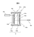
図6は、実施例の画像表示素子の構成を示している。ここでは画像表示素子10は2枚の導光板100a,100bから構成されており,それぞれ入射回折格子101,出射回折格子102が形成される。
図8により、まず,出射回折格子102の具体例について述べる。図8(a)と図8(b)により、同じアスペクト比0.8の場合のフォトニック結晶とメッシュ型回折格子の投影像の比較をした。図8(a)は「特許文献1」に記載のピラー型のフォトニック結晶の斜視図とその投影像のシミュレーション結果である。図8(b)は本実施例のメッシュ型回折格子の斜視図とその投影像のシミュレーション結果である。形状以外の条件は同じである。図に見られるように,アスペクト比1以下の場合,フォトニック結晶では,投影像の中央部の輝度が高く視認性が悪いことがわかる。それに比較して,本実施例のメッシュ型回折格子は低アスペクト比のパターンで良好な投影像を得ることができる。
図9(a)は「特許文献3」と同じ透過型の回折格子のシミュレーション結果である。透過型回折格子は,入射した光が透過回折して,導光板(基板)100内部を伝搬する。入射回折格子101の位置は,導光板100の光源に近い面に形成される。
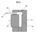
図10Aおよび図10Bは、2枚の導光板100の相対傾きの影響を示す摸式図である。図10Aおよび図10Bにおいて,導光板100はそれぞれ対応波長が異なる導光板100aと100bで構成される。また,300は映像投影用のプロジェクタ,400はユーザの瞳,500は投影される映像光線を表している。
導光板100を伝搬中の光が出射回折格子102で回折して,導光板100から出射する際の回折効率をFDTD法で計算した。波長550nm,導光板の屈折率1.58,回折格子のパターン周期460nm,凸部の幅150nm,凸部の高さ70nmとして,投影像の中央画素に相当する光が入射回折でカップリングして導光板内部を全反射伝搬している条件において,反射回折効率が3.5%,透過回折効率が2.8%となった。凹凸パターンのアスペクト比は0.47である。図10Bと同様に出射回折格子102が,入射回折格子101と同じ面に形成されている場合,ユーザに視認される光線は出射回折格子102で透過回折したものである。したがって,図10Bに示した透過型の光学構成では,図10Aの反射型の光学構成に比較して,ユーザに視認される投影像の輝度が低下してしまう。
導光板100を伝搬中の光が出射回折格子102で回折して,導光板100から出射する際の透過回折効率をFDTD法で計算し,透過回折効率の入射角依存をテーブル化した。これを用いて光線追跡を行い,ユーザが視認する像を求めた。ここでは,波長635nm,導光板の屈折率1.58,回折格子のパターン周期460nm,凸部の幅150nm,凸部の高さ90nmとした。また,導光板100の厚さを1mmとし,入射回折格子101に入射する映像光線の直径は4mm,入射回折格子101と出射回折格子102の間の距離を5mm,導光板100からユーザの瞳400までの距離を25mm,ユーザの瞳400の直径を3mmとした。
本実施例に好適な薄膜材料としては,ZnS,AlN,SiNx,SiO,AlON,Al2O3,等の誘電体材料を用いることができるほか,ZnS-SiO2(20%)のように2種以上の誘電体の混合材料を用いることもできる。
H=(N/N-1)h
となる。
H={(p1+p2)/p1}h
となる。
H=P・tanθB
となる。
この画像表示装置では、プラスチックを導光板100の材料として使用する。図9で説明したように、回折効率の高い入射回折格子では、アスペクト比の高いパターンは作りにくいので、アスペクト比の低くできる反射型の回折格子を入射回折格子101として用いている。反射型の入射回折格子は、導光板100内部に光を反射するので、入射回折格子101は、導光板100の映像光線の入射面(第1面)の反対側の面(第2面)に配置される。
101:入射回折格子
102:出射回折格子
300:プロジェクタ
Claims (4)
- プラスチック基板と、
前記プラスチック基板表面に一体形成され、入射した映像光を回折する入射回折格子と、
前記プラスチック基板表面に一体形成され、前記映像光を出射する出射回折格子と、
前記入射回折格子の凹凸パターンの周期高さをHとしたとき、膜厚d1の第1の誘電体材料と膜厚d2の第2の誘電体材料は交互にN(Nは自然数)周期積層された積層膜を有し、0.7H<d1+d2<1.3Hであり、かつ(d1+d2)×Nが1000nm以下の多層コーティング層と、を備え、
前記多層コーティング層は前記入射回折格子上に設けられ、
前記積層膜の前記プラスチック基板から遠い方の表面は,前記凹凸パターンの形状が反映されていることを特徴とする画像表示素子。 - プラスチック基板と、
前記プラスチック基板表面に一体形成され、入射した映像光を回折する入射回折格子と、
前記プラスチック基板表面に一体形成され、前記映像光を出射する出射回折格子と、
前記入射回折格子の凹凸パターンの周期高さをHとしたとき、膜厚d1の第1の誘電体材料と膜厚d2の第2の誘電体材料は交互にN(Nは自然数)周期積層され、d1+d2がほぼHに等しく、かつ(d1+d2)×Nが1000nm以下の多層コーティング層と、を備え、
前記多層コーティング層は前記入射回折格子上に設けられ、
前記第1の誘電体材料の屈折率をn1,厚さd1とし、前記第2の誘電体材料の屈折率をn2,厚さd2としたとき、
n1>n2、かつ、0.7H<d1+d2<1.3Hであり、
前記Hは、
前記入射回折格子が階段状回折格子であって、その高さがM(Mは2以上の自然数)レベル、最大高さがhの場合、
H=(M/M-1)h
前記入射回折格子がブレーズ型回折格子であって、そのブレーズ角がθB、回折格子周期がpの場合、
H=p・tanθB
前記入射回折格子が一般形状の回折格子であって、その平均傾きから得たブレーズ角がθ、回折格子周期がPの場合、
H=P・tanθ
であることを特徴とする画像表示素子。 - 映像光を形成するための光源であるプロジェクタと、
プラスチック基板と、
前記プラスチック基板表面に一体形成され、入射した映像光を回折する入射回折格子と、
前記プラスチック基板表面に一体形成され、前記映像光を出射する出射回折格子と、
前記出射回折格子上に形成された10nm以上1000nm以下、屈折率が1.4以上2.42以下のコーティング層とを有し、
前記入射回折格子と前記出射回折格子が、前記プラスチック基板の第1の面に形成され、
前記プロジェクタは前記第1の面と反対側の第2の面側に設けられ、
前記プラスチック基板の前記第1の面側から映像光を視認できるように構成され、
前記入射回折格子は反射型回折格子であり、該反射型回折格子の上に多層コーティング層を備え、
前記多層コーティング層は、第1の誘電体薄膜と第2の誘電体薄膜を交互に形成した周期構造を有し、
前記第1の誘電体薄膜の屈折率をn1,厚さd1とし、前記第2の誘電体薄膜の屈折率をn2,厚さd2としたとき、
n1>n2、かつ、0.7H<d1+d2<1.3Hであり、
前記Hは、
前記入射回折格子が階段状回折格子であって、その高さがM(Mは2以上の自然数)レベル、最大高さがhの場合、
H=(M/M-1)h
前記入射回折格子がブレーズ型回折格子であって、そのブレーズ角がθB、回折格子周期がpの場合、
H=p・tanθB
前記入射回折格子が一般形状の回折格子であって、その平均傾きから得たブレーズ角がθ、回折格子周期がPの場合、
H=P・tanθ
であることを特徴とする画像表示装置。 - 映像光を形成するための光源であるプロジェクタと、
プラスチック基板と、
前記プラスチック基板表面に一体形成され、入射した映像光を回折する入射回折格子と、
前記プラスチック基板表面に一体形成され、前記映像光を出射する出射回折格子と、
前記入射回折格子と前記出射回折格子が、前記プラスチック基板の第1の面に形成され、
前記プロジェクタは前記第1の面と反対側の第2の面側に設けられ、
前記プラスチック基板の前記第1の面側から映像光を視認できるように構成され、
前記入射回折格子の凹凸パターンの周期高さをHとしたとき、膜厚d1の第1の誘電体材料と膜厚d2の第2の誘電体材料は交互にN(Nは自然数)周期積層された積層膜を有し、0.7H<d1+d2<1.3Hであり、かつ(d1+d2)×Nが1000nm以下の多層コーティング層と、を備え、
前記多層コーティング層は前記入射回折格子上に設けられ、
前記積層膜の前記プラスチック基板から遠い方の表面は,前記凹凸パターンの形状が反映されていることを特徴とする画像表示装置。
Priority Applications (5)
| Application Number | Priority Date | Filing Date | Title |
|---|---|---|---|
| JP2020002825A JP7341907B2 (ja) | 2020-01-10 | 2020-01-10 | 画像表示素子および装置 |
| US17/782,692 US20230010994A1 (en) | 2020-01-10 | 2020-10-08 | Image display element and device |
| CN202080089119.4A CN114846386B (zh) | 2020-01-10 | 2020-10-08 | 图像显示元件以及图像显示装置 |
| PCT/JP2020/038161 WO2021140717A1 (ja) | 2020-01-10 | 2020-10-08 | 画像表示素子および装置 |
| TW109136214A TWI753617B (zh) | 2020-01-10 | 2020-10-20 | 圖像顯示元件及裝置 |
Applications Claiming Priority (1)
| Application Number | Priority Date | Filing Date | Title |
|---|---|---|---|
| JP2020002825A JP7341907B2 (ja) | 2020-01-10 | 2020-01-10 | 画像表示素子および装置 |
Publications (3)
| Publication Number | Publication Date |
|---|---|
| JP2021110838A JP2021110838A (ja) | 2021-08-02 |
| JP2021110838A5 JP2021110838A5 (ja) | 2022-05-09 |
| JP7341907B2 true JP7341907B2 (ja) | 2023-09-11 |
Family
ID=76788158
Family Applications (1)
| Application Number | Title | Priority Date | Filing Date |
|---|---|---|---|
| JP2020002825A Active JP7341907B2 (ja) | 2020-01-10 | 2020-01-10 | 画像表示素子および装置 |
Country Status (5)
| Country | Link |
|---|---|
| US (1) | US20230010994A1 (ja) |
| JP (1) | JP7341907B2 (ja) |
| CN (1) | CN114846386B (ja) |
| TW (1) | TWI753617B (ja) |
| WO (1) | WO2021140717A1 (ja) |
Citations (8)
| Publication number | Priority date | Publication date | Assignee | Title |
|---|---|---|---|---|
| US20050112510A1 (en) | 2003-09-10 | 2005-05-26 | Asml Netherlands B.V. | Optical element, lithographic apparatus, method for manufacturing and/or protecting an optical element, device manufacturing method and device manufactured thereby |
| JP2007515689A (ja) | 2003-12-23 | 2007-06-14 | オリバ ジョビン イボン エス. アー. エス. | 交互の多層スタックを持つ2次元回折格子ネットワーク、その製法そしてそれらのネットワークを備える分光器 |
| US20100277803A1 (en) | 2006-12-14 | 2010-11-04 | Nokia Corporation | Display Device Having Two Operating Modes |
| US20130100362A1 (en) | 2011-10-24 | 2013-04-25 | Google Inc. | Near-to-eye display with diffraction grating that bends and focuses light |
| US20150293357A1 (en) | 2012-10-18 | 2015-10-15 | Lg Electronics Inc. | Optical device |
| JP2017156388A (ja) | 2016-02-29 | 2017-09-07 | セイコーエプソン株式会社 | 光束径拡大素子及び画像表示装置 |
| US20170307886A1 (en) | 2016-04-25 | 2017-10-26 | Petri Antero Stenberg | Refractive coating for diffractive optical elements |
| WO2020008949A1 (ja) | 2018-07-02 | 2020-01-09 | 株式会社日立エルジーデータストレージ | 導光板、導光板モジュール、画像表示装置および導光板の製造方法 |
Family Cites Families (16)
| Publication number | Priority date | Publication date | Assignee | Title |
|---|---|---|---|---|
| JPH0588151A (ja) * | 1991-09-27 | 1993-04-09 | Matsushita Electric Ind Co Ltd | 液晶パネルとその製造方法および液晶投写型テレビ |
| JPH10133008A (ja) * | 1996-11-01 | 1998-05-22 | Japan Aviation Electron Ind Ltd | 多層膜回折格子およびその製造方法 |
| JP2005115152A (ja) * | 2003-10-09 | 2005-04-28 | Sankyo Seiki Mfg Co Ltd | レンズ、および光ヘッド装置 |
| CN101995594A (zh) * | 2005-08-29 | 2011-03-30 | 松下电器产业株式会社 | 衍射光学元件以及使用衍射光学元件的摄像装置 |
| US20090225424A1 (en) * | 2005-09-30 | 2009-09-10 | Fabian Zimmer | Micro-optical diffraction grid and process for producing the same |
| CN102077127B (zh) * | 2008-12-26 | 2012-10-03 | 松下电器产业株式会社 | 衍射透镜和使用它的摄像装置 |
| CN102236118B (zh) * | 2010-05-07 | 2013-10-16 | 同济大学 | 一种平面结构闪耀光栅 |
| FI125270B (en) * | 2012-09-20 | 2015-08-14 | Teknologian Tutkimuskeskus Vtt Oy | Optical device with diffractive grating |
| US9557458B2 (en) * | 2013-10-29 | 2017-01-31 | CSEM Centre Suisse d'Electronique et de Microtechnique SA—Recherche et Développement | Optical grating coupling structure |
| JP2016048315A (ja) * | 2014-08-27 | 2016-04-07 | Hoya株式会社 | 発色構造体及び外装部品 |
| EP3745167A1 (en) * | 2015-04-07 | 2020-12-02 | Magic Leap, Inc. | Diffraction grating and method of manufacture |
| US10379358B2 (en) * | 2015-04-08 | 2019-08-13 | Despelix Oy | Optical see-through display element and device utilizing such element |
| US10025093B2 (en) * | 2016-04-13 | 2018-07-17 | Microsoft Technology Licensing, Llc | Waveguide-based displays with exit pupil expander |
| JP6410906B1 (ja) * | 2017-09-26 | 2018-10-24 | デクセリアルズ株式会社 | 偏光素子及び光学機器 |
| TWI767081B (zh) * | 2017-10-30 | 2022-06-11 | 美商菲絲博克科技有限公司 | 利用化學輔助反應離子束蝕刻製造傾斜表面浮雕結構的系統及方法 |
| US10845596B2 (en) * | 2018-01-23 | 2020-11-24 | Facebook Technologies, Llc | Slanted surface relief grating for rainbow reduction in waveguide display |
-
2020
- 2020-01-10 JP JP2020002825A patent/JP7341907B2/ja active Active
- 2020-10-08 WO PCT/JP2020/038161 patent/WO2021140717A1/ja active Application Filing
- 2020-10-08 US US17/782,692 patent/US20230010994A1/en active Pending
- 2020-10-08 CN CN202080089119.4A patent/CN114846386B/zh active Active
- 2020-10-20 TW TW109136214A patent/TWI753617B/zh active
Patent Citations (8)
| Publication number | Priority date | Publication date | Assignee | Title |
|---|---|---|---|---|
| US20050112510A1 (en) | 2003-09-10 | 2005-05-26 | Asml Netherlands B.V. | Optical element, lithographic apparatus, method for manufacturing and/or protecting an optical element, device manufacturing method and device manufactured thereby |
| JP2007515689A (ja) | 2003-12-23 | 2007-06-14 | オリバ ジョビン イボン エス. アー. エス. | 交互の多層スタックを持つ2次元回折格子ネットワーク、その製法そしてそれらのネットワークを備える分光器 |
| US20100277803A1 (en) | 2006-12-14 | 2010-11-04 | Nokia Corporation | Display Device Having Two Operating Modes |
| US20130100362A1 (en) | 2011-10-24 | 2013-04-25 | Google Inc. | Near-to-eye display with diffraction grating that bends and focuses light |
| US20150293357A1 (en) | 2012-10-18 | 2015-10-15 | Lg Electronics Inc. | Optical device |
| JP2017156388A (ja) | 2016-02-29 | 2017-09-07 | セイコーエプソン株式会社 | 光束径拡大素子及び画像表示装置 |
| US20170307886A1 (en) | 2016-04-25 | 2017-10-26 | Petri Antero Stenberg | Refractive coating for diffractive optical elements |
| WO2020008949A1 (ja) | 2018-07-02 | 2020-01-09 | 株式会社日立エルジーデータストレージ | 導光板、導光板モジュール、画像表示装置および導光板の製造方法 |
Also Published As
| Publication number | Publication date |
|---|---|
| TWI753617B (zh) | 2022-01-21 |
| JP2021110838A (ja) | 2021-08-02 |
| US20230010994A1 (en) | 2023-01-12 |
| CN114846386A (zh) | 2022-08-02 |
| CN114846386B (zh) | 2024-04-02 |
| WO2021140717A1 (ja) | 2021-07-15 |
| TW202127072A (zh) | 2021-07-16 |
Similar Documents
| Publication | Publication Date | Title |
|---|---|---|
| US20200012031A1 (en) | Image display device | |
| WO2020255482A1 (ja) | 導光板、その製造方法、導光板モジュール、および画像表示装置 | |
| JP4655771B2 (ja) | 光学装置及び虚像表示装置 | |
| US11561393B2 (en) | Light guide plate and image display device | |
| WO2020008949A1 (ja) | 導光板、導光板モジュール、画像表示装置および導光板の製造方法 | |
| JP7341906B2 (ja) | 画像表示素子、画像表示装置および画像表示方法 | |
| JP7341907B2 (ja) | 画像表示素子および装置 | |
| JP7465826B2 (ja) | 導光板、導光板モジュールおよび画像表示装置 | |
| TW202117374A (zh) | 全像波導 |
Legal Events
| Date | Code | Title | Description |
|---|---|---|---|
| A521 | Request for written amendment filed |
Free format text: JAPANESE INTERMEDIATE CODE: A523 Effective date: 20220425 |
|
| A621 | Written request for application examination |
Free format text: JAPANESE INTERMEDIATE CODE: A621 Effective date: 20220425 |
|
| A131 | Notification of reasons for refusal |
Free format text: JAPANESE INTERMEDIATE CODE: A131 Effective date: 20230509 |
|
| A521 | Request for written amendment filed |
Free format text: JAPANESE INTERMEDIATE CODE: A523 Effective date: 20230616 |
|
| TRDD | Decision of grant or rejection written | ||
| A01 | Written decision to grant a patent or to grant a registration (utility model) |
Free format text: JAPANESE INTERMEDIATE CODE: A01 Effective date: 20230829 |
|
| A61 | First payment of annual fees (during grant procedure) |
Free format text: JAPANESE INTERMEDIATE CODE: A61 Effective date: 20230830 |
|
| R150 | Certificate of patent or registration of utility model |
Ref document number: 7341907 Country of ref document: JP Free format text: JAPANESE INTERMEDIATE CODE: R150 |