WO2021130837A1 - 電子源、電子線装置および電子源の製造方法 - Google Patents
電子源、電子線装置および電子源の製造方法 Download PDFInfo
- Publication number
- WO2021130837A1 WO2021130837A1 PCT/JP2019/050481 JP2019050481W WO2021130837A1 WO 2021130837 A1 WO2021130837 A1 WO 2021130837A1 JP 2019050481 W JP2019050481 W JP 2019050481W WO 2021130837 A1 WO2021130837 A1 WO 2021130837A1
- Authority
- WO
- WIPO (PCT)
- Prior art keywords
- electron source
- tip
- electron
- protrusion
- chip
- Prior art date
- Legal status (The legal status is an assumption and is not a legal conclusion. Google has not performed a legal analysis and makes no representation as to the accuracy of the status listed.)
- Ceased
Links
Images











Classifications
-
- H—ELECTRICITY
- H01—ELECTRIC ELEMENTS
- H01J—ELECTRIC DISCHARGE TUBES OR DISCHARGE LAMPS
- H01J9/00—Apparatus or processes specially adapted for the manufacture, installation, removal, maintenance of electric discharge tubes, discharge lamps, or parts thereof; Recovery of material from discharge tubes or lamps
- H01J9/02—Manufacture of electrodes or electrode systems
- H01J9/022—Manufacture of electrodes or electrode systems of cold cathodes
- H01J9/025—Manufacture of electrodes or electrode systems of cold cathodes of field emission cathodes
-
- H—ELECTRICITY
- H01—ELECTRIC ELEMENTS
- H01J—ELECTRIC DISCHARGE TUBES OR DISCHARGE LAMPS
- H01J37/00—Discharge tubes with provision for introducing objects or material to be exposed to the discharge, e.g. for the purpose of examination or processing thereof
- H01J37/02—Details
- H01J37/04—Arrangements of electrodes and associated parts for generating or controlling the discharge, e.g. electron-optical arrangement or ion-optical arrangement
- H01J37/06—Electron sources; Electron guns
- H01J37/075—Electron guns using thermionic emission from cathodes heated by particle bombardment or by irradiation, e.g. by laser
-
- G—PHYSICS
- G01—MEASURING; TESTING
- G01N—INVESTIGATING OR ANALYSING MATERIALS BY DETERMINING THEIR CHEMICAL OR PHYSICAL PROPERTIES
- G01N23/00—Investigating or analysing materials by the use of wave or particle radiation, e.g. X-rays or neutrons, not covered by groups G01N3/00 – G01N17/00, G01N21/00 or G01N22/00
- G01N23/22—Investigating or analysing materials by the use of wave or particle radiation, e.g. X-rays or neutrons, not covered by groups G01N3/00 – G01N17/00, G01N21/00 or G01N22/00 by measuring secondary emission from the material
- G01N23/225—Investigating or analysing materials by the use of wave or particle radiation, e.g. X-rays or neutrons, not covered by groups G01N3/00 – G01N17/00, G01N21/00 or G01N22/00 by measuring secondary emission from the material using electron or ion
- G01N23/2251—Investigating or analysing materials by the use of wave or particle radiation, e.g. X-rays or neutrons, not covered by groups G01N3/00 – G01N17/00, G01N21/00 or G01N22/00 by measuring secondary emission from the material using electron or ion using incident electron beams, e.g. scanning electron microscopy [SEM]
-
- H—ELECTRICITY
- H01—ELECTRIC ELEMENTS
- H01J—ELECTRIC DISCHARGE TUBES OR DISCHARGE LAMPS
- H01J37/00—Discharge tubes with provision for introducing objects or material to be exposed to the discharge, e.g. for the purpose of examination or processing thereof
- H01J37/02—Details
- H01J37/04—Arrangements of electrodes and associated parts for generating or controlling the discharge, e.g. electron-optical arrangement or ion-optical arrangement
- H01J37/06—Electron sources; Electron guns
-
- H—ELECTRICITY
- H01—ELECTRIC ELEMENTS
- H01J—ELECTRIC DISCHARGE TUBES OR DISCHARGE LAMPS
- H01J9/00—Apparatus or processes specially adapted for the manufacture, installation, removal, maintenance of electric discharge tubes, discharge lamps, or parts thereof; Recovery of material from discharge tubes or lamps
- H01J9/02—Manufacture of electrodes or electrode systems
- H01J9/18—Assembling together the component parts of electrode systems
-
- G—PHYSICS
- G01—MEASURING; TESTING
- G01N—INVESTIGATING OR ANALYSING MATERIALS BY DETERMINING THEIR CHEMICAL OR PHYSICAL PROPERTIES
- G01N2223/00—Investigating materials by wave or particle radiation
- G01N2223/07—Investigating materials by wave or particle radiation secondary emission
-
- G—PHYSICS
- G01—MEASURING; TESTING
- G01N—INVESTIGATING OR ANALYSING MATERIALS BY DETERMINING THEIR CHEMICAL OR PHYSICAL PROPERTIES
- G01N2223/00—Investigating materials by wave or particle radiation
- G01N2223/20—Sources of radiation
-
- G—PHYSICS
- G01—MEASURING; TESTING
- G01N—INVESTIGATING OR ANALYSING MATERIALS BY DETERMINING THEIR CHEMICAL OR PHYSICAL PROPERTIES
- G01N2223/00—Investigating materials by wave or particle radiation
- G01N2223/40—Imaging
- G01N2223/418—Imaging electron microscope
-
- H—ELECTRICITY
- H01—ELECTRIC ELEMENTS
- H01J—ELECTRIC DISCHARGE TUBES OR DISCHARGE LAMPS
- H01J2237/00—Discharge tubes exposing object to beam, e.g. for analysis treatment, etching, imaging
- H01J2237/06—Sources
- H01J2237/061—Construction
-
- H—ELECTRICITY
- H01—ELECTRIC ELEMENTS
- H01J—ELECTRIC DISCHARGE TUBES OR DISCHARGE LAMPS
- H01J2237/00—Discharge tubes exposing object to beam, e.g. for analysis treatment, etching, imaging
- H01J2237/06—Sources
- H01J2237/063—Electron sources
- H01J2237/06308—Thermionic sources
- H01J2237/06316—Schottky emission
Definitions
- the present invention relates to an electron source, an electron beam device, and a method for manufacturing an electron source.
- the electron microscope has a spatial resolution that exceeds the optical limit, and can observe the fine structure on the order of nm to pm and analyze the composition. Therefore, it is widely used in engineering fields such as materials, physics, medicine, biology, electricity, and machinery.
- a scanning electron microscope SEM as a device that can easily observe the sample surface.
- thermoelectron source Thermal Emitter: TE
- Field Emitter: FE Field Emitter
- SE Schottky Emission electron source
- FIG. 1 shows an energy diagram showing the operating principles of a thermionic source, a field emission electron source, and a Schottky emission electron source.
- the thermoelectron source (TE) shown in FIG. 1A heats a tungsten (W) filament processed into a hairpin shape to about 2500 ° C., and heats the electrons thermally excited in the W solid to work function of W.
- the electron e is taken out into the vacuum by crossing the energy barrier of ⁇ (4.3 eV). Since the electron source is constantly heated, the surface of the electron source is not contaminated due to gas adsorption or the like, and a stable electron beam with little current fluctuation can be taken out. On the other hand, since the electron source is heated to a very high temperature, the energy half-value full width ⁇ E TE of the emitted electrons is as wide as 3 to 4 eV, and since electrons are emitted from the entire heated part, the electron emission area is wide and the light source. luminance B because of the size (unit area, the emission current amount per unit solid angle) is 10 5 a / cm 2 sr as low as about.
- a thermionic source of hexaboride such as LaB 6 having a work function ⁇ lower than W is also used.
- LaB 6 thermionic source can reduce the operating temperature due to the low work function ⁇ is up to about 1400 ⁇ 1600 ° C., the energy FWHM Delta] E TE can be suppressed to 2 ⁇ 3 eV, the luminance B also increased to about 10 6 A / cm 2 sr It is possible.
- thermal electron sources greater energy FWHM Delta] E TE is, but low spatial resolution for chromatic aberration increases the electron optical system such as the electron microscope objective lens, is easy to handle inexpensive simplified scanning electron It is used as an electron source for a microscope (SEM), a transmission electron microscope (TEM: Transmission Electron Microscope) having a high acceleration voltage and less influence of chromatic aberration, and the like.
- SEM microscope
- TEM Transmission Electron Microscope
- the field emission electron source (FE) shown in FIG. 1B has good monochromaticity and can emit a high-brightness electron beam, it can reduce chromatic aberration of the electron optics system and is used for a scanning electron microscope having high spatial resolution. It is used as an electron source. Normally, it is used as a cold field emission electron source (CFE: Cold Field Emitter) used at room temperature, but a thermal field emission electron source (TFE: Thermal Field Emitter) used by heating to about several hundred degrees Celsius to suppress gas adsorption and the like. There is also. A tungsten (W) chip with a sharp tip is widely used as a cold field emission electron source (CFE).
- CFE cold field emission electron source
- TFE Thermal Field Emitter
- the electrons e in the W chip are effectively thinned by thinning the energy barrier, so that they are permeated by a quantum mechanical tunnel phenomenon and released into a vacuum. Since it can operate at room temperature, the half-value full width at half maximum ⁇ E FE of the extracted electrons e is as narrow as about 0.3 eV, and since electrons are emitted from the narrow electron emission area at the tip of a very sharp chip, the light source size is small and the brightness is high. It has a high feature of 10 8 A / cm 2 sr.
- a cold field emission electron source using a hexaboride nanowire such as LaB 6 having a low work function ⁇ has also been proposed in order to further narrow the energy half width ⁇ E FE and increase the brightness B of the field emission electron source (for example).
- Patent Document 1 A cold field emission electron source using a hexaboride nanowire such as LaB 6 having a low work function ⁇ has also been proposed in order to further narrow the energy half width ⁇ E FE and increase the brightness B of the field emission electron source (for example).
- Patent Document 1 The work function barrier is lower than that of W, and the tunnel probability near the Fermi surface can be increased at a lower electric field, so that the energy half width ⁇ E FE can be further reduced.
- a ZrO / W Schottky emission electron source (ZrO / W) in which zirconium oxide (ZrO 2 ) is applied to a W chip and thermally diffused on a W (100) crystal plane ( SE) is used.
- the ZrO / W Schottky emission electron source is constantly heated to about 1400 to 1500 ° C., and ZrO thermally diffused to the tip of the W chip lowers the work function ⁇ of the (100) plane of the W chip to about 2.8 eV.
- Thermoelectrons are emitted beyond the energy barrier of the work function ⁇ lowered by the Schottky effect of the external electric field F applied to the tip of the chip and the mirror image potential.
- the Schottky emission electron source can stably extract a large current density than the field emission electron source, but since the operating temperature is high, the energy half-value full width ⁇ E SE is as large as about 0.6 to 1 eV.
- the inventors have used hexaborated single crystals such as CeB 6 produced by the floating zone method, etc., and made full use of electrolytic polishing, focused ion beam processing (Focused Ion Beam, FIB), field emission, etc. at the tip. Then, the radius of curvature of the tip is processed to about 50 to 150 nm or 300 to 500 nm, and further heat treatment such as flushing and annealing is performed at 1000 ° C to 1400 ° C for about 5 seconds to 10 minutes in a vacuum to achieve a work function.
- CFE cold field emission electron source
- This field emission electron source has better monochromaticity than the field emission electron source of the conventional W chip, and the energy half width ⁇ E FE at the same radiation angle current density is 0.08 eV to 0.14 eV narrower than that of W.
- the ratio J ⁇ / It of the radiation angle current density J ⁇ ( ⁇ A / sr) to the total current It is 6 times or more, and the radiation angle current density is high.
- An electronic source can be realized. According to the present invention, it is possible to improve the chromatic aberration of a scanning electron microscope particularly at a low acceleration voltage, and to improve the spatial resolution of observing the polar surface of a sample and observing a light element substance such as a carbon-based compound.
- a field emission electron source using a hexaborized single crystal such as CeB 6 has high brightness and good monochromaticity of emitted electrons, and can reduce chromatic aberration of an electron optical system such as an objective lens, so that it can be used as a scanning electron microscope with high spatial resolution.
- the work function is lower than that of a field emission electron source such as W, it becomes relatively sensitive to fluctuations in the work function due to gas adsorption, and the problem is that the stability of the emitted current is inferior.
- TFE field emission electron source
- SE Schottky electron source
- Unnecessary side emission increases the total current It per radiation angle current density J ⁇ , so that the high-voltage power supply applied to the extraction electrode requires a large current capacity, which leads to an increase in equipment cost.
- the amount of electron shock desorption gas generated at the extraction electrode increases, the degree of vacuum decreases, the amount of gas adsorbed on the chip increases, which hinders current stabilization of the electron source, and in some cases, discharge destruction of the chip, etc. It may be a cause of defects.
- electrons having irregular energy and emission directions are emitted from the tip of the chip and mixed with the main beam to cause noise and flare in the image of the electron microscope, which is not preferable because the image quality is deteriorated.
- the present invention provides a method for manufacturing an electron source, an electron beam device, and an electron source that prevent the occurrence of side emissions in a field emission electron source or a shotkey emission electron source using a hexaborized single crystal. To do.
- One aspect of the present invention for achieving the above object is a protrusion that emits electrons when an electric field is generated, a shank that supports the protrusion and is reduced in diameter toward the protrusion, and a body that supports the shank.
- the shank and the body are composed of hexaboride single crystal, and the shank and part of the body excluding the protrusion are covered with a material having a higher work function than the hexaboride single crystal. It is an electron source characterized by being.
- Another aspect of the present invention for achieving the above object is an electron source, a sample table on which a sample is placed, an electron gun optical system having an extraction electrode and an acceleration electrode for extracting electrons from the electron source, and emission.
- An electron beam apparatus comprising an electron optics system that focuses and irradiates a sample on a sample table with the generated electrons, and the electron source is the above-mentioned electron source of the present invention.
- Another aspect of the present invention for achieving the above object is a protrusion that emits electrons when an electric field is generated, a shank that supports the protrusion and is reduced in diameter toward the protrusion, and a shank.
- a method for producing an electron source which comprises a step of forming a film having a work function larger than that of a single crystal and a step of removing a mask to expose the protruding portion.
- the present invention it is possible to provide a method for manufacturing an electron source, an electron beam device, and an electron source that prevent the occurrence of side emissions in a field emission electron source or a Schottky emission electron source using a hexaborized single crystal. it can.
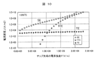
- Thermionic emission component (TE), Schottky emission component (SE), and thermal field emission component (TFE) of the emission current when chips with project lengths L of 5 ⁇ m, 20 ⁇ m, 50 ⁇ m, and 100 ⁇ m are operated at 1350 ° C.
- the present inventors have studied intensively, the portion excluding the electron emitting portion of a chip made of hexaboride single crystal such as CeB 6 developed for cold field emission electron source (CFE) far hexaboride single crystal
- CFE cold field emission electron source
- FIG. 2 is a schematic view showing an example of the electron beam apparatus of the present invention
- FIG. 3 is an SEM observation photograph in which the tip portion of the electron source of FIG. 2 is enlarged.
- the electron beam apparatus 200 of the present embodiment is roughly divided into an electron source (electron gun) 120 that emits electrons to generate an electron beam 106 and an electron beam generated from the electron source 120.
- An electron optical system 130 for converging and irradiating the sample 115 with the 106 is provided.
- the electron source 120 has an electron source (emitter) 100 that emits electrons, an extraction electrode 105, and an acceleration electrode 108.
- the electron source 100 is controlled to be constantly heated by passing a constant current by a heating power source 103 controlled by a computer 101 and a controller 102.
- the extraction electrode 105 applies a positive voltage to the tip tip (not shown) of the electron source 100 by the extraction power supply 104 to emit electrons by the Schottky effect or the thermal field emission effect.
- the emitted electron beam 106 is accelerated toward the grounded acceleration electrode (anode) 108 by the negative high voltage applied by the acceleration power source 107 that gives an electric potential to the chip.
- the electro-optical system 130 includes a first condenser lens 109, an aperture 110, a second condenser lens 111, an objective lens 112, an astigmatic correction coil 113, and a deflection scanning coil 114.
- the electron beam 106 accelerated by the accelerating electrode 108 is focused by the first condenser lens 109, the aperture 110, the second condenser lens 111, the objective lens 112, and the non-point correction coil 113, and is scanned by the deflection scanning coil 114 to sample 115.
- the upper observation area is irradiated, and the generated secondary electrons are detected by the secondary electron detector 116.
- the detector may be placed between the objective lens and the sample in addition to the position shown in the figure, and can be switched and used depending on the operating conditions of the device. Although the detector is not shown except for the secondary electron detector, a backscattered electron detector, an elemental analyzer, and the like are also used.
- the electron source 100 has a chip 43 made of a hexaboride single crystal.
- the tip of the chip 43 has a protruding portion (electron emitting portion) 40 that emits electrons, a shank 41 that supports the protruding portion 40 and is reduced in diameter toward the protruding portion, and a body portion 42 that supports the shank 41. ..
- the shank 41 and a part of the body portion 42 are covered with a material having a higher work function than the hexaboride single crystal, except for the protruding portion 40 of the chip 43.
- the hexaboride for example, CeB 6 is preferable.
- Carbon is preferable as a material having a higher work function than the hexaboride single crystal.
- the electrons emitted from the CeB 6 shot key emission electron source or the CeB 6 thermal field emission electron source 100 have a narrow half-value full width and good monochromaticity, so that chromatic aberration in the objective lens 112 and the like is reduced, and the electrons are narrowed down.
- the beam 106 can be applied to the sample 115, and a highly resolved scanning electron microscope image can be obtained. Further, since the radiation angle current density is high, the imaging time can be shortened and the analysis time such as elemental analysis can be shortened. Furthermore, since the emission current has high long-term stability, it is also suitable for application of electron microscopes used in mass production factories such as measuring the length of semiconductor devices in semiconductor factories.
- FIG. 4 is a schematic diagram showing a unit cell of CeB 6.
- CeB 6 has a crystal structure in which six blocks of boron atoms 2 are located at the center of the simple cubic lattice of Ce atoms 1.
- the work function of CeB 6 is about 2.6 eV, which is much lower than that of W, which is about 4.3 eV, and Ce has f electrons with strong energy localization and high state density just below the Fermi level. It has a high density of electrons that pass through the work function barrier due to field emission and electrons that are excited by heating, and is suitable as a material for producing a field emission electron source or a Schottky emission electron source with a large current density.
- the hexaboride LaB 6 and the like are preferable in addition to CeB 6.
- FIG. 5 is a graph showing the relationship between the electric field strength F (V / m) at the tip of the hexaboride single crystal chip using CeB 6 and the total current It ( ⁇ A) of electron emission. As shown in FIG.
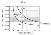
- FIG. 6 is a graph showing the relationship between the radius of curvature R ( ⁇ m) at the tip of the chip using the CeB 6 single crystal and the electric field strength F (V / m) at the tip of the chip.
- R radius of curvature
- F electric field strength
- FIG. 6 it is shown as a function of the extraction voltage V1 of the electron microscope.
- the radius of curvature of the tip of the chip should be at least 1.2 ⁇ m or less over the entire control range of V1. It must be 0.8 ⁇ m or less to be controllable.
- the electric field intensity of 1.5 ⁇ 10 9 V / m required for thermal-field emission is at least 0.8 ⁇ m or less, is required to be 0.5 ⁇ m or less to be controlled by the overall control range of V1 .. If the electric field is set too high for the Schottky emission electron source, thermal field emission electrons are mixed, which is not preferable.
- the lower limit of the radius of curvature of the tip of the chip is set to 0.3 ⁇ m, more preferably 0.4 ⁇ m. Also, in the case of a thermal field emission electron source, if the chip diameter is too small, it cannot be controlled within the voltage control range of V1, so the lower limit of the radius of curvature is 0.2 ⁇ m, more preferably 0.3 ⁇ m.
- thermoelectron emission occurs from the entire chip when heated.
- the current density of thermionic emission is low, since the area of the entire chip is large, the total current is larger than the current obtained by thermal field emission or Schottky emission, and there is a problem that there are many unnecessary currents. Therefore, it is necessary to coat a carbon film having a higher work function than a hexaboride single crystal such as CeB 6 to suppress thermionic emission.
- the coating of the carbon film may also be applied to the thermionic source, and the thickness of the carbon film is usually 1 ⁇ m or more in order to sufficiently suppress the thermionic emission.
- the radius of curvature of the tip of the chip is very small, about 0.2 to 1.2 ⁇ m, as described above. If a carbon film having a thickness of 1 ⁇ m or more is formed on the side wall of the chip, the shape of the tip of the chip changes significantly, and there is a problem that the electric field is difficult to concentrate on the tip of the chip. Further, a high electric field is applied to the end face of the carbon film, and unnecessary field emission is likely to occur, which causes a problem that the operation of the electron source becomes unstable.
- the relationship between the length L of the protruding portion of the hexaboride single crystal not coated with the carbon film and the field distribution near the tip of the chip and the amount of thermionic emission generated from the protruding portion is investigated, and the optimum carbon film thickness is investigated. I found a range.
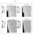
- FIG. 7 is a graph showing the electric field strength distribution near the tip of the chip when the length L of the protruding portion is (a) 1 ⁇ m, (b) 5 ⁇ m, (c) 20 ⁇ m, and (d) 50 ⁇ m.
- the length L of the protruding portion is (a) 1 ⁇ m and almost all the electrons other than the semicircular electron emission at the tip of the chip are covered with the carbon film, the tip other than the tip of the chip is covered. It can be seen that a strong electric field is also applied to the end face of the carbon film (the portion surrounded by the dotted line in FIG. 7A).
- the electric field on the end face of this carbon film sharply decreases by increasing the length L of the protruding portion to (b) 5 ⁇ m and (c) 20 ⁇ m, and at (d) 50 ⁇ m, it is almost the same as the electric field normally applied to the chip side wall. It drops to strength.
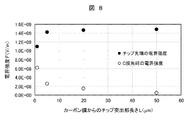
- FIG. 8 is a graph showing the relationship between the length L of the protruding portion at the tip of the chip and the electric field strength F (V / m).
- the thickness of the carbon film was 1 ⁇ m. Looking at FIG. 8, when the length L of the protruding portion is 1 ⁇ m, not only the electric field at the end face of the carbon film is strong, but also the electric field strength at the tip of the hexaboride single crystal is lowered, so that it can be used as an electron source. Has a very unstable structure.
- the field intensity of the tip point when the length L than 5 ⁇ m of protrusions stable at approximately 1.5 ⁇ 10 about 9 V / m
- the electric field strength F (V / m) of the carbon film edge even chips Since it is reduced to about 1/10 of the tip, a stable electric field distribution can be formed, and a stable structure can be realized as an electron source.
- the thermionic emission component (TE) is 3 to 9 ⁇ A, and if the electric field strength at the tip of the chip is increased to 1 ⁇ 10 9 V / m or more, the Schottky emission component (SE) Can be the main one.
- the thermionic emission component (TE) is 33 to 97 ⁇ A
- the thermionic emission component (TE) is 70 to 200 ⁇ A, 1.5 ⁇
- the optimum length L of the protruding portion is 5 to 20 ⁇ m.
- TE is about two orders of magnitude lower than SE in terms of current density, so even if L is 50 to 100 ⁇ m, the SE component has a sufficiently large amount of current emitted from the tip of the chip, and a high-intensity electron source. Can be used as. However, if it exceeds this value, the current capacity of the high-voltage power supply of the extraction electrode used in a normal electron microscope becomes large, the stability of the voltage is impaired, and the stabilization circuit becomes expensive, which is not preferable. In addition, the amount of electron shock desorption gas increases, the emission current becomes unstable due to a decrease in the degree of vacuum in the electron gun chamber, and the risk of discharge damage increases, which is not preferable. Therefore, L is preferably 5 to 100 ⁇ m, more preferably 5 to 20 ⁇ m. A method for producing an electron source having such a protruding portion L will be described later.
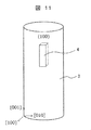
- FIG. 11 is a schematic view showing a hexaboride single crystal.
- a hexaboride single crystal such as CeB 6 has a diameter of several mm due to melt (liquid phase) crystal growth using, for example, a floating zone method, and is perpendicular to the (100) plane of the crystal habit plane in which the crystal grows preferentially.
- a large single crystal 3 having a length of several tens of mm grown in the crystal axis direction can be produced.
- the single crystal 3 was cut into a chip 4 having a square shape of several hundred ⁇ m and a length of several mm by cutting, and the (100) plane was used as an electron emission plane.
- the (100) plane was used as an electron emission plane.
- FIGS. 12 to 18 are schematic views showing a joining process of hexaboride chips. Subsequently, a bonding method for holding the hexaboride chip and attaching a filament for heating will be described with reference to FIGS. 12 to 18.
- a metal tube such as tantalum or niobium and a hexaboride tip arranged inside the metal tube are provided with a plurality of recesses from at least two axial directions on the outer circumference of the metal tube so as to surround the central axis.
- FIG. 12 is a flow chart showing a manufacturing process of a metal tube.
- the material of the metal tube is a refractory metal such as tantalum or niobium, which is highly ductile, and is suitable for a material in which a minute metal tube can be easily formed by drawing a tube and a recess, which will be described later, can be easily processed.
- tantalum was used as an example.
- the metal sheet 5 of tantalum is rolled, and both ends 6 of the metal sheet 5 are electron beam welded to prepare a semi-seamless tube 7 of tantalum having a large diameter. Subsequently, by repeating the drawing and drawing tube processing using the die 8, a metal pipe 9 having an outer diameter of ⁇ 500 ⁇ m, an inner diameter of ⁇ 320 ⁇ m, and a wall thickness of 90 ⁇ m is produced, and further cut into small pieces by a cutter 10 every 5 mm. Metal tube 12 was produced.
- the inner diameter of the metal tube 12 is set to about 1.1 to 1.5 times the maximum diameter of the chip 4. It is preferable to keep it. If it is 1.1 times or less, the processing tolerance of the chip 4 is usually about 10%, so that the number of chips 4 that cannot be inserted into the metal tube 12 increases, and the manufacturing yield of the electron source decreases. On the other hand, if it is 1.5 times or more, the dimensional difference between the inner diameters of the chip 4 and the metal tube 12 becomes too large, and the amount of deformation of the metal tube 12 in the process of forming and joining the recess described later is large, resulting in a decrease in assembly accuracy. The strength is lowered, the heat capacity is increased due to the volume increase of the metal tube 12, the power consumption is increased, and the heating responsiveness is lowered.
- the inner diameter of the metal tube 12 is preferably in the range of 310 to 423 ⁇ m. In this embodiment, the inner diameter of the metal tube 12 is 320 ⁇ m.
- the filament needs to be spot-welded to the metal tube 12, and the metal tube 12 needs to have sufficient strength because it needs to withstand high-temperature heating during operation for a long time.
- the wall thickness is too thick, the heat capacity of the metal tube 12 increases, which leads to a decrease in the heating responsiveness of the electron source and an increase in heating power.
- the wall thickness may be 50 ⁇ m or more. In the present invention, the wall thickness is 90 ⁇ m.
- FIG. 13 is a schematic view showing a step of inserting a hexaboride into a metal tube.
- the metal tube 12 is vertically erected using a pedestal 14 in which a guide pin 13 having a diameter of 300 ⁇ m and a length of 1 to 3 mm that enters the inner diameter of the metal tube 12 is vertically erected.
- the hexaboride tip 4 is inserted from the upper part of the metal tube 12.
- the guide pin 13 can control the length (protrusion amount) A of the hexaboride tip 4 protruding from the inside of the metal tube 12.
- the protrusion amount is lengthened to 2 to 3 mm in order to scrape the hexaboride chip 4 by electrolytic polishing as described later.
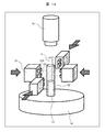
- the hexaboride tip 4 and the metal tube 12 are pressure-welded with a special tool from two orthogonal axes and four directions in a plane perpendicular to the vertical direction of the tip 4.
- a special tool from two orthogonal axes and four directions in a plane perpendicular to the vertical direction of the tip 4.
- FIG. 14 only the portion of the blade 15 of the pressure welding tool is shown in consideration of the legibility of the drawing.
- two-stage protrusions 150 and 151 for forming a recess in the metal pipe 12 are provided, and the metal pipe is brought closer to the metal pipe 12 from two axes and four directions with an even stroke.
- a recess is formed by crushing from the outer circumference of 12.
- each side surface of the hexaboride tip 4 of the square column coincides with the stroke directions of the tool protrusions 150 and 151.
- the rotation axis of the chip 4 is adjusted as appropriate.
- a plurality of recesses are formed so as to surround the central axis from the outer circumference of the metal tube 12, and the bottom of each recess contacts the outer peripheral surface of the hexaboride tip, so that the hexaboride tip 4 is automatically formed. It can be fixed along the central axis of the metal tube 12.
- the bonding force is increased by joining even at the points deviated in the axial direction, and the tip 4 is tilted at the joining part by joining at the two points in the axial direction. This can be prevented and has the effect of increasing the accuracy of centering.
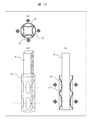
- FIG. 15 is a schematic view of a joint between the hexaboride tip 4 and the metal tube 12.
- (A) shows a cross-sectional view of the joint portion seen from the tip side of the chip 4, and (c) also shows a cross-sectional view of the center of the chip 4 in the vertical direction.
- the metal tube 12 and the hexaboride tip 4 can be pressure-welded evenly from two axes and four directions, and a mechanically strong bond can be obtained.
- the hexaboride tip 4 of the square pillar is automatically aligned with the central axis of the metal tube 12. Since the assembly accuracy is improved, the electron source can be easily aligned and the yield is also improved. Since the dotted line portion into which the guide pin 13 has been inserted becomes unnecessary, the metal tube 12 is cut with a cutter to reduce the heat capacity.
- a filament 18 such as tungsten is directly spot-welded to the metal tube 12 to which the hexaboride tip 4 is joined, and both ends of the filament 18 are spot-welded to the electrode 20 of the stem 19. Since these are metal-to-metal joints, it is possible to easily obtain a strong joint by spot welding.
- the alignment jig 21 is used as shown in FIG. First, the filament 18 such as tungsten is accurately aligned with the metal tube 12 using the alignment jig 21-1 and spot welded, and then the stem 19 and the metal tube 12 are aligned with the metal tube 12 using the alignment jig 21-2. If spot welding is performed by accurately aligning the above, the central axes of the metal tube 12 and the hexaboride chip 4 are aligned, so that highly accurate axis alignment is possible.
- the chip 4 cut into a square columnar shape was used.
- the tip 4 may be processed into a cylinder.
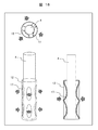
- FIG. 18 is an example in the case where the cylindrical tip 4 is used.
- the chip 4 of the square pillar it is naturally acceptable to join from two axes and four directions.
- the tip of the hexaboride chip 4 assembled as shown in FIG. 19 is dipped in an electrolytic solution 22 such as nitric acid, and an alternating current is formed between the tip 4 and the counter electrode 23 such as platinum formed in a ring shape. This is done by applying a voltage from the DC power supply 24. As shown in FIG. 20, the tip 4 of the hexaboride forms a meniscus on the liquid surface when immersed in the electrolytic polishing liquid, and the polishing speed of the liquid surface portion is slow and the polishing speed of the submerged portion is high.
- an electrolytic solution 22 such as nitric acid
- the counter electrode 23 such as platinum formed in a ring shape
- FIG. 21 is an SEM observation photograph of the tip of the hexaboride single crystal chip.
- FIG. 21 shows an SEM image of a hexaboride tip obtained by processing a quadrangular column tip into a quadrangular pyramid having a tapered tip. Since electrolytic polishing basically proceeds isotropically, it is possible to process the columnar chip into an isotropic quadrangular pyramid or conical shape if the shape of the columnar chip is a quadrangular column or a column.
- FIG. 22 is an SEM observation photograph of the tip of the hexaboride chip, and shows an SEM image of the hexaboride chip whose tip is hemispherically processed by electrolytic polishing again with respect to the chip shown in FIG. 21.
- the tip of the chip can be rounded into a hemispherical shape by electric field evaporation.
- Electric field evaporation is a method in which atoms on the tip surface are ionized and gradually stripped off by applying an electric field of a positive electrode of + several tens of V / nm to an electron source. Electric field evaporation occurs preferentially in places where the electric field strength is strong. For this reason, atoms on sharp points and steps on the surface evaporate, and the entire surface can be evaporated over time. Eventually, when the electric field evaporation progresses sufficiently, the tip of the electron source becomes a hemispherical shape in which the electric field strength is even over the entire surface.
- FIG. 23 is an SEM observation photograph of the tip of the hexaboride chip, and shows an SEM image of the hexaboride chip whose tip is hemispherically rounded by electric field evaporation.
- FIG. 24 is a schematic view showing a method of forming a coating film on the tip of a hexaboride single crystal chip.
- the purpose of coating carbon is to suppress unnecessary thermionic emission from the chip side wall when the electron source is heated to operate as a thermofield electron emission source or Schottky emission electron source. ..
- a chip base material (chip before carbon coating) is prepared, and a mask material 27 for preventing coating of a carbon film is applied to a part of the chip tip 25 and the shank 26.
- the mask material 27 examples include novolak resins used for photoresists, resist materials such as polyethylene glycol used as water-soluble resists, ionic liquids having excellent heat resistance and abundant variations in viscosity and solubility, and peeling. An electrowax having excellent properties can be used. Specifically, the tip tip 25 is immersed in a mask material 27 such as a resist liquid, an ionic liquid, or a melt of electrowax dissolved by heating, and then the chip is pulled up to apply the mask material 27. Although not shown, the mask material 27 may be discharged from a microdispenser and applied to the tip tip.
- a mask material 27 such as a resist liquid, an ionic liquid, or a melt of electrowax dissolved by heating
- the carbon film 29 is formed using a sputtering device capable of forming a film at room temperature and the carbon target 28.
- the resist material does not thermally condense or the electrowax does not remelt, and functions as a mask material 27 to prevent the carbon film 29 from being coated on the protruding portion 30 including the tip tip 25. Can be done.
- the resist material, the ionic liquid, the mask material 27 such as electrowax, and the like are peeled off from the chip.
- the resist material can be dissolved and peeled by immersing it in a stripping liquid (dedicated alkaline stripping liquid, organic solvent, water, etc.).
- electrowax is generally a material with good mold releasability, and can be easily peeled off from the chip mechanically.
- the carbon film 29 on the mask material 27 is also peeled off at the same time, so that the hexaboride chip is exposed only in the protruding portion 30 including the tip tip 25, and the other chip side walls are coated with the carbon film 29.
- the source can be made.
- FIG. 17 shows an example of an SEM photograph of the created electron source.
- FIG. 25 is an SEM observation photograph of the hexaboride single crystal chip.
- the protrusion length L of the protrusion 30 of the hexaboride single crystal from the carbon film 29 is 15 ⁇ m.
- a coating film is formed even at the tip of the chip, and then the coating film at the tip is physically peeled off by machining.
- a chip having a minute tip portion (tip radius of curvature R: 1.2 ⁇ m or less) as in the present invention cannot be subjected to such processing.
- a coating film can be formed on the tip portion excluding the electron emitting portion of the chip.
Landscapes
- Chemical & Material Sciences (AREA)
- Analytical Chemistry (AREA)
- Physics & Mathematics (AREA)
- Manufacturing & Machinery (AREA)
- Engineering & Computer Science (AREA)
- Health & Medical Sciences (AREA)
- Optics & Photonics (AREA)
- Life Sciences & Earth Sciences (AREA)
- Biochemistry (AREA)
- General Health & Medical Sciences (AREA)
- General Physics & Mathematics (AREA)
- Immunology (AREA)
- Pathology (AREA)
- Electron Sources, Ion Sources (AREA)
- Cold Cathode And The Manufacture (AREA)
Priority Applications (3)
| Application Number | Priority Date | Filing Date | Title |
|---|---|---|---|
| US17/781,267 US12494338B2 (en) | 2019-12-24 | 2019-12-24 | Electron source, electron beam device, and method for manufacturing electron source |
| JP2021566413A JP7295974B2 (ja) | 2019-12-24 | 2019-12-24 | 電子源、電子線装置および電子源の製造方法 |
| PCT/JP2019/050481 WO2021130837A1 (ja) | 2019-12-24 | 2019-12-24 | 電子源、電子線装置および電子源の製造方法 |
Applications Claiming Priority (1)
| Application Number | Priority Date | Filing Date | Title |
|---|---|---|---|
| PCT/JP2019/050481 WO2021130837A1 (ja) | 2019-12-24 | 2019-12-24 | 電子源、電子線装置および電子源の製造方法 |
Publications (1)
| Publication Number | Publication Date |
|---|---|
| WO2021130837A1 true WO2021130837A1 (ja) | 2021-07-01 |
Family
ID=76575750
Family Applications (1)
| Application Number | Title | Priority Date | Filing Date |
|---|---|---|---|
| PCT/JP2019/050481 Ceased WO2021130837A1 (ja) | 2019-12-24 | 2019-12-24 | 電子源、電子線装置および電子源の製造方法 |
Country Status (3)
| Country | Link |
|---|---|
| US (1) | US12494338B2 (https=) |
| JP (1) | JP7295974B2 (https=) |
| WO (1) | WO2021130837A1 (https=) |
Cited By (1)
| Publication number | Priority date | Publication date | Assignee | Title |
|---|---|---|---|---|
| US11651924B1 (en) | 2022-06-22 | 2023-05-16 | Fei Company | Method of producing microrods for electron emitters, and associated microrods and electron emitters |
Citations (4)
| Publication number | Priority date | Publication date | Assignee | Title |
|---|---|---|---|---|
| JPS6147038A (ja) * | 1984-07-02 | 1986-03-07 | ジエイソン ジヨン キム | 熱電子陰極とその製造方法 |
| JP2000173900A (ja) * | 1998-12-08 | 2000-06-23 | Canon Inc | 電子ビーム照明装置、および該照明装置を用いた電子ビーム露光装置 |
| WO2008120412A1 (ja) * | 2007-03-29 | 2008-10-09 | Advantest Corporation | 電子銃及び電子ビーム露光装置 |
| JP2019525401A (ja) * | 2016-06-30 | 2019-09-05 | ケーエルエー コーポレイション | 高輝度でホウ素を含有する真空環境用電子ビームエミッタ |
Family Cites Families (8)
| Publication number | Priority date | Publication date | Assignee | Title |
|---|---|---|---|---|
| JP4939565B2 (ja) | 2009-04-06 | 2012-05-30 | キヤノン株式会社 | 電子ビーム露光装置 |
| JP2011146250A (ja) | 2010-01-14 | 2011-07-28 | Nuflare Technology Inc | 電子銃用のエミッタ使用方法 |
| JP5595199B2 (ja) | 2010-09-23 | 2014-09-24 | 株式会社ニューフレアテクノロジー | 電子銃および電子銃を用いた電子ビーム描画装置 |
| US8952605B2 (en) | 2012-07-03 | 2015-02-10 | National Institute For Materials Science | Metal hexaboride cold field emitter, method of fabricating same, and electron gun |
| US9165737B2 (en) * | 2012-10-04 | 2015-10-20 | Nuflare Technology, Inc. | High-brightness, long life thermionic cathode and methods of its fabrication |
| WO2018016286A1 (ja) * | 2016-07-19 | 2018-01-25 | デンカ株式会社 | 電子源およびその製造方法 |
| CN109804450B (zh) | 2016-10-13 | 2020-12-01 | 株式会社日立高新技术 | 电子束装置 |
| JP6636472B2 (ja) | 2017-02-28 | 2020-01-29 | 株式会社日立ハイテクノロジーズ | 電子源およびそれを用いた電子線装置 |
-
2019
- 2019-12-24 JP JP2021566413A patent/JP7295974B2/ja active Active
- 2019-12-24 WO PCT/JP2019/050481 patent/WO2021130837A1/ja not_active Ceased
- 2019-12-24 US US17/781,267 patent/US12494338B2/en active Active
Patent Citations (4)
| Publication number | Priority date | Publication date | Assignee | Title |
|---|---|---|---|---|
| JPS6147038A (ja) * | 1984-07-02 | 1986-03-07 | ジエイソン ジヨン キム | 熱電子陰極とその製造方法 |
| JP2000173900A (ja) * | 1998-12-08 | 2000-06-23 | Canon Inc | 電子ビーム照明装置、および該照明装置を用いた電子ビーム露光装置 |
| WO2008120412A1 (ja) * | 2007-03-29 | 2008-10-09 | Advantest Corporation | 電子銃及び電子ビーム露光装置 |
| JP2019525401A (ja) * | 2016-06-30 | 2019-09-05 | ケーエルエー コーポレイション | 高輝度でホウ素を含有する真空環境用電子ビームエミッタ |
Cited By (2)
| Publication number | Priority date | Publication date | Assignee | Title |
|---|---|---|---|---|
| US11651924B1 (en) | 2022-06-22 | 2023-05-16 | Fei Company | Method of producing microrods for electron emitters, and associated microrods and electron emitters |
| CN117301327A (zh) * | 2022-06-22 | 2023-12-29 | Fei 公司 | 生产用于电子发射器的微棒的方法及相关联的微棒和电子发射器 |
Also Published As
| Publication number | Publication date |
|---|---|
| JP7295974B2 (ja) | 2023-06-21 |
| JPWO2021130837A1 (https=) | 2021-07-01 |
| US12494338B2 (en) | 2025-12-09 |
| US20220415603A1 (en) | 2022-12-29 |
Similar Documents
| Publication | Publication Date | Title |
|---|---|---|
| US8764994B2 (en) | Method for fabricating emitter | |
| JP2015518245A5 (https=) | ||
| JP6999277B2 (ja) | 熱電界エミッタチップ、熱電界エミッタチップを含む電子ビーム装置、および電子ビーム装置を動作させる方法 | |
| JP7403678B2 (ja) | 電子源とその製造方法およびそれを用いた電子線装置 | |
| JP5564689B2 (ja) | 電界電離型ガスイオン源のエミッタおよびこれを備えた集束イオンビーム装置ならびに電界電離型ガスイオン源のエミッタの製造方法 | |
| JP6112930B2 (ja) | ガスイオン源、及び集束イオンビーム装置 | |
| EP2242084B1 (en) | Method of manufacturing an electron source | |
| JP7295974B2 (ja) | 電子源、電子線装置および電子源の製造方法 | |
| KR100264365B1 (ko) | 니들 전극 및 전자 에미터용 니들 전극의 제조방법 | |
| US10658143B2 (en) | Method of manufacturing emitter | |
| JP4792404B2 (ja) | 電子源の製造方法 | |
| KR20010080286A (ko) | 열전계 방출 정렬 방법 및 장치 | |
| JP7022837B2 (ja) | 電子源とその製造方法およびそれを用いた電子線装置 | |
| JP3250724B2 (ja) | 針状電極の製造方法 | |
| US20250316438A1 (en) | Field emission electron source, method of producing same, and electron beam device using same | |
| US11081312B2 (en) | Method of manufacturing emitter, emitter, and focused ion beam apparatus | |
| WO2025253467A1 (ja) | ショットキー電子源、ショットキー電子源の製造方法および電子線装置 | |
| JP2010238367A (ja) | 高効率ダイヤモンド電子銃 |
Legal Events
| Date | Code | Title | Description |
|---|---|---|---|
| 121 | Ep: the epo has been informed by wipo that ep was designated in this application |
Ref document number: 19957796 Country of ref document: EP Kind code of ref document: A1 |
|
| ENP | Entry into the national phase |
Ref document number: 2021566413 Country of ref document: JP Kind code of ref document: A |
|
| NENP | Non-entry into the national phase |
Ref country code: DE |
|
| 122 | Ep: pct application non-entry in european phase |
Ref document number: 19957796 Country of ref document: EP Kind code of ref document: A1 |
|
| WWG | Wipo information: grant in national office |
Ref document number: 17781267 Country of ref document: US |