WO2021124382A1 - 荷電粒子ビーム装置 - Google Patents
荷電粒子ビーム装置 Download PDFInfo
- Publication number
- WO2021124382A1 WO2021124382A1 PCT/JP2019/049124 JP2019049124W WO2021124382A1 WO 2021124382 A1 WO2021124382 A1 WO 2021124382A1 JP 2019049124 W JP2019049124 W JP 2019049124W WO 2021124382 A1 WO2021124382 A1 WO 2021124382A1
- Authority
- WO
- WIPO (PCT)
- Prior art keywords
- switching circuit
- electrode
- charged particle
- blanking
- particle beam
- Prior art date
- Legal status (The legal status is an assumption and is not a legal conclusion. Google has not performed a legal analysis and makes no representation as to the accuracy of the status listed.)
- Ceased
Links
Images










Classifications
-
- H—ELECTRICITY
- H01—ELECTRIC ELEMENTS
- H01J—ELECTRIC DISCHARGE TUBES OR DISCHARGE LAMPS
- H01J37/00—Discharge tubes with provision for introducing objects or material to be exposed to the discharge, e.g. for the purpose of examination or processing thereof
- H01J37/02—Details
- H01J37/04—Arrangements of electrodes and associated parts for generating or controlling the discharge, e.g. electron-optical arrangement or ion-optical arrangement
- H01J37/045—Beam blanking or chopping, i.e. arrangements for momentarily interrupting exposure to the discharge
-
- H—ELECTRICITY
- H01—ELECTRIC ELEMENTS
- H01J—ELECTRIC DISCHARGE TUBES OR DISCHARGE LAMPS
- H01J37/00—Discharge tubes with provision for introducing objects or material to be exposed to the discharge, e.g. for the purpose of examination or processing thereof
- H01J37/02—Details
- H01J37/04—Arrangements of electrodes and associated parts for generating or controlling the discharge, e.g. electron-optical arrangement or ion-optical arrangement
- H01J37/09—Diaphragms; Shields associated with electron or ion-optical arrangements; Compensation of disturbing fields
-
- H—ELECTRICITY
- H01—ELECTRIC ELEMENTS
- H01J—ELECTRIC DISCHARGE TUBES OR DISCHARGE LAMPS
- H01J37/00—Discharge tubes with provision for introducing objects or material to be exposed to the discharge, e.g. for the purpose of examination or processing thereof
- H01J37/02—Details
- H01J37/04—Arrangements of electrodes and associated parts for generating or controlling the discharge, e.g. electron-optical arrangement or ion-optical arrangement
- H01J37/147—Arrangements for directing or deflecting the discharge along a desired path
-
- H—ELECTRICITY
- H01—ELECTRIC ELEMENTS
- H01J—ELECTRIC DISCHARGE TUBES OR DISCHARGE LAMPS
- H01J37/00—Discharge tubes with provision for introducing objects or material to be exposed to the discharge, e.g. for the purpose of examination or processing thereof
- H01J37/02—Details
- H01J37/24—Circuit arrangements not adapted to a particular application of the tube and not otherwise provided for
-
- H—ELECTRICITY
- H01—ELECTRIC ELEMENTS
- H01J—ELECTRIC DISCHARGE TUBES OR DISCHARGE LAMPS
- H01J37/00—Discharge tubes with provision for introducing objects or material to be exposed to the discharge, e.g. for the purpose of examination or processing thereof
- H01J37/26—Electron or ion microscopes; Electron or ion diffraction tubes
- H01J37/28—Electron or ion microscopes; Electron or ion diffraction tubes with scanning beams
Definitions
- the present invention relates to a charged particle beam device, and can be used particularly for a charged particle beam device that blocks an electron beam by blanking.
- a charged particle beam device represented by a scanning electron microscope or the like irradiates a sample with a charged particle beam, converts backscattered electrons or secondary electrons from the sample into an electric signal by a detector such as a scintillator or a photomultiplier tube. It is a device that measures the dimensions of fine patterns formed on a sample through an amplification circuit, an arithmetic processing circuit, and a display.
- Patent Document 1 Japanese Unexamined Patent Publication No. 2019-133789
- a blanking control circuit is disclosed in which the electrodes on the opposite sides of the two opposing electrodes on the blanking electrodes of each stage arranged in the same direction and the ground are connected to each other.
- the blanking when the blanking is ON, the positive voltage is output to the remaining electrodes of the upper blanking electrode, and the negative voltage is output to the remaining electrodes of the lower blanking electrode.
- the blanking is OFF, the same ground reference signal is output to the remaining electrodes of the upper blanking electrode and the remaining electrodes of the lower blanking electrode.
- noise is applied to the blanking electrode when the blanking control circuit that blocks the electron beam is OFF, the electron beam is irradiated in an unintended direction, and there is a problem that the measurement accuracy is lowered.
- the noise added to the blanking electrode includes noise entering from the GND terminal and power supply noise.
- Patent Document 1 describes that a noise electric field is generated in the upper and lower two-stage blanking electrodes in the opposite direction, and the fluctuation of the electron beam due to the noise electric field is canceled by the upper and lower two-stage blanking electrodes to reduce noise. ing.
- the upper and lower two-stage blanking electrodes have different deflection sensitivities with respect to the electron beam. Therefore, in order to cancel the noise electric field with the upper and lower two-stage blanking electrodes, it is necessary to have a means for adjusting the noise voltage applied to the blanking electrodes according to the deflection sensitivity, which is very difficult to realize.
- the noise targeted by Patent Document 1 is assumed to be noise invading from the GND terminal of the blanking control circuit, and power supply noise is not considered.
- An object of the present invention is to solve the above-mentioned problems of the prior art and to provide a charged particle beam device provided with a low noise blanking control circuit.
- the charged particle beam device includes a stage on which a sample can be mounted, a charged particle gun that ejects charged particles to the sample, a voltage source, and a first switching circuit in which a voltage is supplied from the voltage source. , A second switching circuit with one end connected to the ground, a third switching circuit with one end connected to the ground, a fourth switching circuit to which voltage is supplied from a voltage source, a first switching circuit, and a second switching circuit.
- the second blanking electrode, the first switching circuit, and the first blanking electrode which are connected to the first blanking electrode and are connected to the third switching circuit and the fourth switching circuit, which face the first blanking electrode. It has two switching circuits, a third switching circuit, and a control circuit for controlling a fourth switching circuit.
- the performance of the charged particle beam device can be improved.
- the measurement accuracy can be improved.
- FIG. 5 is a waveform diagram showing a blanking control signal and a voltage applied to a blanking electrode in the blanking control circuit according to the third embodiment of the present invention. It is a circuit diagram which shows the blanking control circuit which concerns on the modification of Embodiment 3 of this invention. It is a waveform diagram which shows the blanking control signal and the voltage applied to the blanking electrode in the blanking control circuit which concerns on the modification of Embodiment 3 of this invention. It is a circuit diagram which shows the blanking control circuit which concerns on Embodiment 4 of this invention.
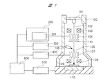
- FIG. 1 is a schematic view showing an example of the configuration of the charged particle beam device according to the first embodiment of the present invention.
- the charged particle beam device includes a column (electron optical lens barrel) 100, a charged particle gun (electron gun) 101 that irradiates (injects) an electron beam (charged particle beam) 102, and an electron beam 102.
- the focusing lens 103 is provided.
- the charged particle beam device further changes the direction of the electron beam 102, deflects the deflection electrode 107 that controls the position of scanning the electron beam 102 on the sample 109 to be measured, and deflects the electron beam 102 to hit the aperture 111.
- the charged particle beam device includes a plurality of blanking electrodes 104 that block irradiation on the sample 109, and an objective lens 108 that refocuses the electron beam 102.
- the charged particle beam device further includes a movable stage 110 on which the sample 109 is mounted, and a detector 105 that detects secondary electrons 106 emitted from the sample 109 irradiated and scanned by the electron beam 102. ing.
- the charged particle beam device includes an electro-optical control unit 200 (including a blanking control circuit 201), a signal detection / image processing unit 300, a deflection control unit 400, a mechanism control unit 500, and an overall control unit 600.
- the overall control unit 600 performs a process of controlling the entire charged particle beam device. For example, the overall control unit 600 performs measurement / inspection processing by controlling the electron optics control unit 200, the deflection control unit 400, the mechanism control unit 500, and the like according to the measurement / inspection conditions. When the measurement / inspection is executed, the overall control unit 600 receives the image data generated through the signal detection / image processing unit 300 and displays it on a GUI (Graphical User Interface) screen or the like.
- GUI Graphic User Interface
- the blanking electrode 104 is composed of a set of two metal plates arranged in parallel with each other. That is, the two metal plates are arranged so as to face each other.
- the electro-optical control unit 200 controls the electro-optical system (focusing lens 103, blanking electrode 104, and objective lens 108) in the column 100 according to the control from the overall control unit 600.
- the blanking control circuit 201 applies a blanking voltage to the blanking electrode 104 through the signal line based on the blanking control signal supplied from the overall control unit 600, so that the sample 109 of the electron beam 102 ON / OFF control of upward irradiation is performed.
- the blanking control signal When the blanking control signal is ON, a voltage is applied to the blanking electrode 104 to generate an electric field between the electrodes, and the electron beam 102 is deflected and cut off by the aperture 111. Therefore, the electron beam 102 does not irradiate the sample 109. Further, when the blanking control signal is OFF, no voltage is applied to the blanking electrode 104, so that no electric field is generated between the electrodes, and the electron beam 102 passes through the aperture 111 and irradiates the sample 109.
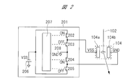
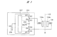
- FIGS. 2 and 3 show an example of a conceptual diagram of the blanking control circuit 201 according to the first embodiment.
- the blanking electrode 104 of the present embodiment has the first electrode (blanking electrode) 104a and the first electrode (blanking electrode) 104a facing each other in a direction perpendicular to the irradiation direction of the electron beam 102 with the irradiation position of the electron beam 102 in the air in the center.
- a second electrode (blanking electrode) 104b is provided.
- the blanking control circuit 201 turns on the switching circuits 202 to 205 based on the switching circuits 202 to 205, the voltage source 206 that generates (generates) a negative voltage (VSS), and the blanking control signal from the overall control unit 600.
- VSS negative voltage
- a driver circuit 207 for controlling / OFF is provided. That is, the driver circuit 207 can control each of the switching circuits 202 to 205 to either an ON state (conducting state) or an OFF state (non-conducting state).
- the switching circuit referred to here may be a circuit in which a plurality of elements are connected, or may be a switching element composed of a single element.
- the negative voltage (VSS) output of the voltage source 206 is connected to the first electrode 104a via the switching circuit 202, and is connected to the second electrode 104b via the switching circuit 205.
- the common ground (common ground reference point, common GND) 208 provided on the blanking control circuit 201 is connected to the first electrode 104a via the switching circuit 203, and is also connected to the first electrode 104a via the switching circuit 204. It is connected to the electrode 104b.
- the common ground 208 is referred to as a common GND 208.
- the blanking control circuit 201 has a switching circuit (first switching circuit) 202 to which a voltage is supplied from the voltage source 206, a switching circuit (second switching circuit) 203 having one end connected to a common GND 208, and one end being common.
- the switching circuit (third switching circuit) 204 connected to the GND 208 and the switching circuit (fourth switching circuit) 205 to which the voltage is supplied from the voltage source 206 are provided.
- FIG. 2 shows a state in which the blanking control signal is ON.
- the driver circuit 207 connects the negative voltage (VSS) to the first electrode 104a by turning on the switching circuits 202 and 204 and turning off the switching circuits 203 and 205, and the GND 208 common to the second electrode 104b.
- a negative voltage (VSS) is applied to the first electrode 104a
- a GND potential is applied to the second electrode 104b.
- a blanking electric field is generated in the direction from the second electrode 104b to the first electrode 104a, and the electron beam 102 can be deflected.
- the blanking electric field is indicated by a white arrow.
- FIG. 3 shows a state in which the blanking control signal is OFF.
- the driver circuit 207 connects the common GND 208 to the first electrode 104a and the second electrode 104b by turning on the switching circuits 203 and 204 and turning off the switching circuits 202 and 205.
- no blanking electric field is generated between the first electrode 104a and the second electrode 104b, and the electron beam 102 irradiates the sample 109.
- FIG. 4 shows a circuit diagram as a specific configuration example of the blanking control circuit 201 according to the present embodiment.
- the switching circuits 202 and 205 are N-channel MOSFETs (Metal Oxide Semiconductor Field Effect Transistors) 12 and 15.
- the sources (source terminals) of the N-channel MOSFETs 12 and 15 are connected to a negative voltage (VSS), and the gate (gate terminal) is connected to the driver circuit 207.
- the drain (drain terminal) of the N-channel MOSFET 12 is connected to the first electrode 104a, and the drain of the N-channel MOSFET 15 is connected to the second electrode 104b.
- the switching circuits 203 and 204 are P-channel MOSFETs 13 and 14.
- the sources of the P-channel MOSFETs 13 and 14 are connected to a common GND 208, and the gate is connected to the driver circuit 207.
- the drain of the P-channel MOSFET 13 is connected to the first electrode 104a, and the drain of the P-channel MOSFET 14 is connected to the second electrode 104b.
- FIG. 4 shows the power supply noise 209 and the GND noise 210 in order to explain the low noise effect in the present embodiment.
- the power supply noise 209 is, for example, noise output by the voltage source 206, and includes high-frequency spike noise or ripple noise associated with switching.
- the GND noise 210 is a noise component generated in a common GND 208. For example, the GND potential fluctuation caused by the return of the current consumed by the element or the like on the blanking control circuit 201 flowing through the GND, the noise generated by another circuit on the charged particle beam device, or the like is conducted to the GND noise 210.
- the noise or the like mixed in the blanking control circuit 201 by radiation is included.
- FIG. 4 shows the electron beam 2ON as the orbit of the electron beam 102 when the blanking is ON, and the electron beam 2OFF as the orbit of the electron beam 102 when the blanking is OFF. This also applies to FIGS. 5 to 9, 11 and 13 which will be used later.
- the driver circuit 207 turns on the N-channel MOSFET 12 and the P-channel MOSFET 14 and turns off the P-channel MOSFET 13 and the N-channel MOSFET 15 so that the first electrode 104a has a negative voltage ( VSS) is connected, and the common GND208 is connected to the second electrode 104b.
- VSS negative voltage
- the common GND208 is connected to the second electrode 104b.
- the driver circuit 207 turns off the N-channel MOSFETs 12 and 15 and turns on the P-channel MOSFETs 13 and 14, so that the GND 208 common to the first electrode 104a and the second electrode 104b can be used. Connecting. At this time, the GND noise 210 is conducted to the first electrode 104a and the second electrode 104b, respectively, via the on-resistance of the P-channel MOSFETs 13 and 14, respectively. Since the GND noise 210 is applied to the first electrode 104a and the second electrode 104b with the same amplitude and phase, no electric field due to the GND noise 210 is generated between the electrodes.
- the power supply noise 209 is conducted to the first electrode 104a and the second electrode 104b, respectively, via the parasitic capacitance mainly between the drain and the source of the N-channel MOSFETs 12 and 15.
- the power supply noise 209 since the first electrode 104a and the second electrode 104b are applied with the same amplitude and the same phase, no electric field due to the power supply noise 209 is generated between the electrodes. Therefore, low noise can be realized.
- noise may be applied to one of the opposing blanking electrodes when the blanking control circuit is OFF.
- the blanking control circuit is OFF, it is important to prevent the electron beam from being deflected by noise and to irradiate the sample straight with the electron beam.
- the N-channel MOSFET 12 connected between the voltage source 206 and the first electrode 104a and the N-channel MOSFET 15 connected between the voltage source 206 and the second electrode 104b are common.
- a P-channel MOSFET 13 connected between the GND 208 and the first electrode 104a and a P-channel MOSFET 14 connected between the common GND 208 and the second electrode 104b are provided.
- both the N-channel MOSFETs 12 and 15 are turned off. Even if both the N-channel MOSFETs 12 and 15 are OFF, the power supply noise 209 is conducted to the first electrode 104a and the second electrode 104b mainly through the parasitic capacitance between the drain and the source of the N-channel MOSFETs 12 and 15. However, since the same power supply noise 209 is applied to each of the first electrode 104a and the second electrode 104b, it is possible to prevent an electric field due to the noise from being generated between the electrodes.
- the P-channel MOSFETs 13 and 14 are both turned on. At this time, since the GND noise 210 is similarly applied to each of the first electrode 104a and the second electrode 104b, it is possible to prevent an electric field due to the noise from being generated between the electrodes.
- the blanking electrode 104 even when the power supply noise 209 and the GND noise 210 are large, no noise electric field is generated between the blanking electrodes 104, and low noise can be realized. Therefore, it is possible to design the blanking electrode 104 to have a short distance between the electrodes.
- the sensitivity of the blanking electrode 104 (deflection distance per applied voltage) is higher as the distance between the electrodes is shorter. Therefore, by shortening the distance between the electrodes, it is possible to obtain the sensitivity required for deflecting the highly accelerated electron beam with only a pair of blanking electrodes 104. Also, it is not necessary to increase the blanking voltage in order to deflect the highly accelerated electron beam.
- the blanking response speed can be improved (the time required for switching the irradiation / blocking of the electron beam 102 shown in FIG. 1 to the sample 109 can be shortened).
- the FET element may be, for example, a bipolar transistor.
- the gate, source, and drain, which are the terminals of the MOSFET of the above-described embodiment, are replaced with the base, emitter, and collector, which are the terminals of the bipolar transistor, respectively. That is, for example, each of the N-channel MOSFETs 12 and 15 shown in FIG. 4 is replaced with an NPN-type bipolar transistor, and each of the P-channel MOSFETs 13 and 14 is replaced with a PNP-type bipolar transistor.
- the emitter terminals of the NPN-type bipolar transistors that replace the N-channel MOSFETs 12 and 15 are connected to the voltage source 206, and the emitter terminals of the PNP-type bipolar transistors that replace the P-channel MOSFETs 13 and 14 are connected to the common GND 208. Further, the NPN-type bipolar transistor that replaces the N-channel MOSFET 12 and the collector terminal of the PNP-type bipolar transistor that replaces the P-channel MOSFET 13 are connected to the first electrode 104a. The PNP type bipolar transistor replacing the P channel MOSFET 14 and the collector terminal of the NPN type bipolar transistor replacing the N channel MOSFET 15 are connected to the second electrode 104b.
- FIG. 5 shows a circuit diagram of the blanking control circuit 201 in the first modification of the present embodiment.
- the voltage source 206 outputs (generates) a positive voltage (VDD)
- the switching circuits 202 and 205 are P-channel MOSFETs
- the switching circuits 203 and 204 are a point composed of N-channel MOSFETs.
- the driver circuit 207 turns on the P-channel MOSFET 22 and the N-channel MOSFET 24 and turns off the N-channel MOSFET 23 and the P-channel MOSFET 25, so that the first electrode 104a has a positive voltage ( VDD) is connected, and the common GND208 is connected to the second electrode 104b.
- VDD positive voltage
- the common GND208 is connected to the second electrode 104b.
- the driver circuit 207 turns off the P-channel MOSFETs 22 and 25 and turns on the N-channel MOSFETs 23 and 24, so that the GND 208 common to the first electrode 104a and the second electrode 104b is turned on. Connecting. At this time, since the GND noise 210 is applied to the first electrode 104a and the second electrode 104b with the same amplitude and the same phase via the N-channel MOSFETs 23 and 24, respectively, no electric field due to the GND noise 210 is generated between the electrodes.
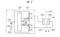
- FIG. 6 shows a circuit diagram of the blanking control circuit 201 in the second modification of the present embodiment.
- the switching circuits 202 and 205 are configured by being replaced with resistors 32 and 35, and the switching circuits 203 and 204 are configured by P-channel MOSFETs 33 and 34. That is the point.
- the driver circuit 207 only needs to control ON / OFF of only the P channels MOSFETs 33 and 34.
- resistors 32 and 35 resistors of the same type, resistors having the same notation, or resistors having the same resistance value are used.
- the configurations of the P-channel MOSFETs 33 and 34 are the same as the configurations of the P-channel MOSFETs 13 and 14, respectively shown in FIG.
- the driver circuit 207 turns off the P-channel MOSFET 33 and turns on the P-channel MOSFET 34, so that a negative voltage (VSS) is applied to the first electrode 104a via the resistor 32.
- the common GND 208 is connected to the second electrode 104b via the P channel MOSFET 34.
- the driver circuit 207 connects the common GND 208 to the first electrode 104a and the second electrode 104b by turning on the P channels MOSFETs 33 and 34.
- the GND noise 210 is applied to the first electrode 104a and the second electrode 104b with the same amplitude and the same phase via the P-channel MOSFETs 33 and 34, respectively, no electric field due to the GND noise 210 is generated between the electrodes.
- the power supply noise 209 is applied to the first electrode 104a and the second electrode 104b with the same amplitude and the same phase through the resistors 32 and 35, respectively, an electric field due to the power supply noise 209 does not occur between the electrodes. Therefore, low noise can be realized.
- FIG. 7 shows a circuit diagram of the blanking control circuit 201 in the third modification of the present embodiment.
- the difference from the blanking control circuit 201 in FIG. 2 is that the switching circuits 203 and 204 are replaced with resistors 43 and 44, and the switching circuits 202 and 205 are composed of N-channel MOSFETs 42 and 45. That is the point.
- the driver circuit 207 only needs to control ON / OFF of only the N-channel MOSFETs 42 and 45.
- resistors 43 and 44 resistors of the same type, resistors having the same notation, or resistors having the same resistance value are used.
- the configurations of the N-channel MOSFETs 42 and 45 are the same as the configurations of the N-channel MOSFETs 12 and 15, respectively shown in FIG.
- the driver circuit 207 connects the negative voltage (VSS) to the first electrode 104a by turning on the N-channel MOSFET 42 and turning off the N-channel MOSFET 45, and the second A common GND208 is connected to the electrode 104b via a resistor 44.
- VSS negative voltage
- the driver circuit 207 turns off the N-channel MOSFETs 42 and 45 to connect a common GND 208 to the first electrode 104a and the second electrode 104b via resistors 43 and 44. To do. At this time, since the GND noise 210 is applied to the first electrode 104a and the second electrode 104b with the same amplitude and the same phase via the resistors 43 and 44, respectively, no electric field due to the GND noise 210 is generated between the electrodes.
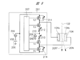
- FIG. 8 shows a circuit diagram of the blanking control circuit 201 according to the present embodiment.
- the configuration shown in FIG. 8 is similar to the configuration shown in FIG. 4, but differs from FIG. 4 in that variable capacitance capacitors 211 and 214 and variable resistors 212 and 213 are provided.
- variable capacitance capacitor 211 is connected between the drain and source terminals of the N channel MOSFET 12, and the variable capacitor 214 is connected between the drain and source terminals of the N channel MOSFET 15. That is, the variable capacitor 211 is connected in parallel to the N channel MOSFET 12, and the variable capacitor 214 is connected in parallel to the N channel MOSFET 15. Further, the variable resistor 212 is connected in series between the common GND 208 and the source terminal of the P channel MOSFET 13, and the variable resistor 213 is connected in series between the common GND 208 and the source terminal of the P channel MOSFET 14. There is.
- variable capacitance capacitors 211 and 214 are provided for the purpose of reducing the individual difference in the parasitic capacitance value between the drain and source terminals between the N channel MOSFETs 12 and 15. That is, for the variable capacitance capacitors 211 and 214, the sum of the drain-source terminal parasitic capacitance of the N-channel MOSFET 12 and the capacitance value of the variable-capacitor capacitor 211 is the drain-source terminal parasitic capacitance and the variable capacitance of the N-channel MOSFET 15. It is desirable to set it so that it matches the value obtained by adding the capacitance value of the capacitor 214.
- variable resistors 212 and 213 are provided for the purpose of reducing the individual difference in the on-resistance value between the drain and source terminals between the P-channel MOSFETs 13 and 14. That is, for the variable resistors 212 and 213, the value obtained by adding the drain-source terminal on-resistance of the P-channel MOSFET 13 and the resistance value of the variable resistor 212 is the value of the drain-source terminal on-resistance of the P-channel MOSFET 14 and the variable resistor 213. It is desirable to set it so that it matches the value obtained by adding the resistance value.
- the impedances of the respective paths from the voltage source 206 to the first electrode 104a and the second electrode 104b can be matched.
- the impedance of each path from the common GND 208 to the first electrode 104a and the second electrode 104b can be matched.
- the power supply noise 209 and the GND noise 210 are applied to the first electrode 104a and the second electrode 104b with the same amplitude and phase, respectively, so that no noise electric field is generated and noise can be reduced.
- the overall control unit 600 receives image data from the signal detection / image processing unit 300, and sets an evaluation index such as resolution or contrast. It may be adjusted to maximize the image quality evaluated using it.
- the variable capacitance capacitor and variable resistor can be adjusted manually by the user in an analog manner. Further, the variable capacitance capacitor and the variable resistor can be digitally controlled from the overall control unit 600, and the capacitance value and the resistance value that maximize the image quality are automatically adjusted by the program incorporated in the overall control unit 600. It can also be configured.
- variable capacitance capacitors 211 and 214, the variable resistors 212 and 213 are provided, and the capacitance value and the resistance value are adjusted so that the wiring impedances from the blanking control circuit 201 to the first electrode 104a and the second electrode 104b are aligned. adjust.
- the power supply noise 209 and the GND noise 210 are applied to the first electrode 104a and the second electrode 104b with the same amplitude and phase, no noise electric field is generated in the blanking electrode 104, and noise can be reduced.
- variable resistor 212 is connected in series between the drain terminal of the P channel MOSFET 13 and the first electrode 104a, and the variable resistor 213 is connected in series between the drain terminal of the P channel MOSFET 14 and the second electrode 104b. It may be a configured configuration. Further, one of the variable capacitance capacitors 211 and 214 may be provided and the other may not be provided. Further, one of the variable resistors 212 and 213 may be provided and the other may not be provided. (Embodiment 3)
- FIG. 9 is a circuit diagram showing an example of the configuration of the blanking control circuit 201 according to the third embodiment of the present invention.
- the configuration shown in FIG. 9 is similar to the configuration shown in FIG. 4, but differs from FIG. 4 in that diodes 215 and 216 are provided.
- the diode 215 has an anode terminal connected to the drain terminal of the P channel MOSFET 13 and a cathode terminal connected to the source side
- the diode 216 has an anode terminal connected to the drain terminal of the P channel MOSFET 14 and a cathode terminal on the source side. It is connected. That is, the diode 215 is connected in parallel to the P-channel MOSFET 13, and the diode 216 is connected in parallel to the P-channel MOSFET 14.
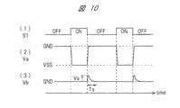
- FIG. 10 shows waveform examples of (1) blanking control signal S1, (2) voltage applied to the first electrode 104a (Va), and (3) voltage applied to the second electrode 104b (Vb). It is a figure.
- the voltage (Va) of the first electrode 104a becomes VSS because the N channel MOSFET 12 is ON.
- the voltage (Vb) of the second electrode 104b becomes a common GND potential because the P channel MOSFET 14 is ON.
- the N-channel MOSFET 12 is turned OFF and the P-channel MOSFET 13 is changed to ON, and a current flows from the common GND 208 toward the first electrode 104a via the P-channel MOSFET 13, and the second electrode is used.
- the voltage (Va) of one electrode 104a changes to a common GND potential.
- a positive voltage (Vs) is induced in the second electrode 104b facing the first electrode 104a.
- the positive voltage (Vs) which is the induced voltage can be limited to the forward voltage or less of the diode 216, so that the second electrode 104b becomes a common GND potential.
- Time (Ts) can be shortened, and the response time can be increased as compared with the case where the diode 216 is not inserted.
- the first electrode can be changed by changing the ON / OFF control method of the switching circuit.
- a blanking electric field can be applied in the direction from 104a to the second electrode 104b.
- the diode 215 contributes to speeding up the response time in the same manner as the diode 216 when the operation of applying the blanking electric field is performed in this way.
- FIG. 11 is a circuit diagram showing a second configuration example of the blanking control circuit 201 according to the third embodiment of the present invention.
- the configuration shown in FIG. 11 is similar to the configuration shown in FIG. 5, but differs from FIG. 5 in that diodes 215 and 216 are provided.
- the diode 215 has an anode terminal connected to the source side of the N-channel MOSFET 23 and a cathode terminal connected to the drain terminal
- the diode 216 has an anode terminal connected to the source terminal of the N-channel MOSFET 24 and a cathode terminal on the drain side. It is connected. That is, the diode 215 is connected in parallel to the N-channel MOSFET 23, and the diode 216 is connected in parallel to the N-channel MOSFET 24.
- FIG. 12 shows waveform examples of (1) blanking control signal S1, (2) voltage applied to the first electrode 104a (Va), and (3) voltage applied to the second electrode 104b (Vb). It is a figure.
- the voltage (Va) of the first electrode 104a becomes VDD because the P channel MOSFET 22 is ON.
- the voltage (Vb) of the second electrode 104b becomes a common GND potential because the N channel MOSFET 24 is ON.
- the P-channel MOSFET 22 When the blanking control signal S1 is switched from ON to OFF, the P-channel MOSFET 22 is turned OFF, the N-channel MOSFET 23 is changed to ON, and a current flows from the first electrode 104a toward the common GND 208 via the N-channel MOSFET 23.
- the voltage (Va) of one electrode 104a changes to a common GND potential.
- a negative voltage (Vd) is induced in the second electrode 104b facing the first electrode 104a.
- the diode 215 contributes to speeding up the response time in the same manner as the diode 216 when the operation of applying a blanking electric field in the direction from the second electrode 104b to the first electrode 104a is performed.
- the fourth embodiment will be described.
- a charged particle beam device capable of reducing the noise electric field generated between the electrodes even when the noise applied to the first electrode and the second electrode is not the same amplitude and phase will be described.
- the description of the parts that overlap with the above-described embodiment will be omitted in principle.
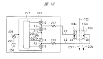
- FIG. 13 is a circuit diagram showing an example of the configuration of the blanking control circuit 201 according to the fourth embodiment of the present invention.
- the configuration shown in FIG. 13 is similar to the configuration shown in FIG. 4, but differs from FIG. 4 in that resistors 217 and 218 are provided.
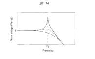
- FIG. 14 is a graph showing an example of the frequency characteristics of the noise voltage (Va-Vb) applied to the blanking electrode 104 when the noise between the connection point P1 and the connection point P2 is set to 1 at a low frequency.
- the graph when there is no resistance is shown by a solid line
- the graph when the resistance value is small is shown by a two-dot chain line
- the graph when the resistance value is large is shown by a one-dot chain line.
- the resistor 217 is inserted between the connection point P1 between the drain terminals of the N-channel MOSFET 12 and the P-channel MOSFET 13 and the first electrode 104a. That is, the resistor 217 is connected in series between the connection point P1 and the first electrode 104a.
- the resistor 218 is inserted between the connection point P2 between the drain terminals of the P-channel MOSFET 14 and the N-channel MOSFET 15 and the second electrode 104b. That is, the resistor 218 is connected in series between the connection point P2 and the second electrode 104b.
- the increase in noise at the resonance point can be reduced by inserting resistors 217 and 218, and the larger the resistance value, the greater the reduction effect.
- the resistance value is increased, the response speed of blanking decreases due to the effect of the low-pass filter, so it is desirable that the resistance value is about several tens of ⁇ to several hundreds of ⁇ .
- the resistors 217 and 218 use the same type of resistor, the resistor having the same notation, or the resistor having the same resistance value to match the wiring impedance.
- power supply noise 209 and GND noise 210 can be added to the first electrode 104a and the second electrode 104b with the same amplitude and phase, so that noise can be reduced.
- FIG. 15 is a circuit diagram showing an example of the configuration of the blanking control circuit 201 and the blanking electrode 104 according to the fifth embodiment of the present invention.
- the blanking electrode 104 in the present embodiment includes two sets of two electrodes facing each other in a direction perpendicular to the irradiation direction of the electron beam 102, with the irradiation position of the electron beam 102 in the air in the center.
- One set of the two sets of electrodes is the first electrode 301a and the second electrode 301b, and the other set of electrodes is the third electrode 301c and the fourth electrode 301d.
- the blanking control circuit 201 includes N-channel MOSFETs 12, 15, 52, 55, P-channel MOSFETs 13, 14, 53, 54, a voltage source 206 that generates a negative voltage (VSS), and an overall control unit 600 (see FIG. 1). It is provided with a driver circuit 207 that controls ON / OFF of the MOSFET based on a blanking control signal from.
- the negative voltage (VSS) output of the voltage source 206 is connected to the respective source terminals of the N-channel MOSFETs 12, 15, 52 and 55.
- a common GND 208 provided on the blanking control circuit 201 is connected to the respective source terminals of the P-channel MOSFETs 13, 14, 53 and 54.
- the gate terminals of all MOSFETs are connected to the driver circuit 207.
- drain terminals of the N-channel MOSFET 12 and the P-channel MOSFET 13 are connected to each other and connected to the first electrode 301a.
- the drain terminals of the P-channel MOSFET 14 and the N-channel MOSFET 15 are connected to each other and connected to the second electrode 301b.
- the drain terminals of the N-channel MOSFET 52 and the P-channel MOSFET 53 are connected to each other and connected to the third electrode 301c.
- the drain terminals of the P-channel MOSFET 54 and the N-channel MOSFET 55 are connected to each other and connected to the fourth electrode 301d.
- FIG. 16 is a plan view showing the positional relationship of the electron beam 102 in the deflection direction by blanking in the present embodiment.
- FIG. 16 is a view of the irradiation direction of the electron beam 102 viewed from the side of the charged particle gun 101 that irradiates the electron beam 102.
- a negative voltage VSS
- a common GND208 is connected to the second electrode 301b and the third electrode 301c. Just do it.
- the blanking electric field applied in the direction from the second electrode 301b to the first electrode 301a and the blanking electric field applied in the direction from the third electrode 301c to the fourth electrode 301d are added.
- a blanking electric field is formed in the direction A2, and the electron beam 102 is deflected in the direction A1 opposite to the blanking electric field.
- a common GND208 is connected to the electrodes arranged on both sides in the direction to be deflected, and a negative voltage (VSS) is connected to the remaining electrodes.
- the operation of the blanking control circuit 201 may be controlled so as to be performed.
- the operation of the blanking control circuit 201 will be described with respect to the case where a blanking electric field is applied in the direction A1.
- the driver circuit 207 turns on the N-channel MOSFETs 12 and 55 and turns off the P-channel MOSFETs 13 and 54, so that the first electrode 301a and the fourth electrode 301d are respectively turned on. Connect the negative voltage (VSS). Further, the driver circuit 207 connects the common GND 208 to each of the second electrode 301b and the third electrode 301c by turning on the P-channel MOSFETs 14 and 53 and turning off the N-channel MOSFETs 15 and 52. As a result, a blanking electric field is generated in the direction A2 in FIG. 16, and the electron beam 102 can be deflected in the direction A1.
- the driver circuit 207 turns off the N-channel MOSFETs 12 and 55 and turns on the P-channel MOSFETs 13 and 54, so that the GND 208 common to the first electrode 301a and the fourth electrode 301d is turned on. Connecting.
- the driver circuit 207 connects the common GND 208 to the second electrode 301b and the third electrode 301c by turning on the P-channel MOSFETs 14 and 53 and turning off the N-channel MOSFETs 15 and 52.
- a common GND 208 is connected to all the electrodes, and a blanking electric field is not generated.
- the GND noise 210 is applied to the first electrode 301a to the fourth electrode 301d with the same amplitude and phase via the P-channel MOSFETs 13, 14, 53, and 54, respectively, so that the noise due to the GND noise 210 is generated between the electrodes. No electric field is generated.
- the power supply noise 209 is applied to the first electrode 301a to the fourth electrode 301d with the same amplitude and phase, respectively, via the parasitic capacitance between the drain terminal and the source terminal of the N channel MOSFETs 12, 15, 52, 55. No electric field is generated between the electrodes due to power supply noise 209. Therefore, low noise can be realized.
- a blanking control circuit 201 in which a switching circuit is connected to each electrode plate is provided to form a blanking electric field in four directions. can do.
- a blanking control circuit 201 in which a switching circuit is connected to each electrode plate is provided to form a blanking electric field in four directions.
- the configuration in which the four blanking electrode plates are provided has been described, but it is also possible to provide more electrode plates and deflect the blanking direction in more plurality of directions.
- a blanking control circuit 201 in which a switching circuit is connected to each electrode plate is provided, and the switching circuit is selectively controlled by the driver circuit 207. It is feasible. (Embodiment 6)
- a charged particle beam device capable of deflecting an electron beam at a large angle by providing two sets of opposing electrode plates arranged one above the other will be described.
- the description of the parts that overlap with the above-described embodiment will be omitted in principle.
- FIG. 17 is a circuit diagram showing an example of the configuration of the blanking control circuit 201 and the blanking electrode 104 according to the sixth embodiment.
- the configuration shown in FIG. 17 is similar to the configuration shown in FIG. 15, but the arrangement of the blanking electrodes 104 is different from that in FIG.
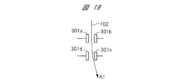
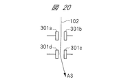
- the blanking electrode 104 in the present embodiment sandwiches a plane along the irradiation direction of the electron beam 102 in the center, and two electrodes facing each other in a direction perpendicular to the plane. It has a configuration in which two sets are arranged in the upper and lower stages. Of these two sets of electrodes, the upper one set is a first electrode 301a and a second electrode 301b in which the electrodes are arranged in parallel with each other and close to the irradiation position of the electron beam 102. Further, of the two sets of electrodes, the lower one set is a third electrode 301c and a fourth electrode 301d in which the electrodes are arranged in parallel with each other and close to the irradiation position of the electron beam 102.
- FIG. 18 to 21 are side views showing the positional relationship of the electron beam 102 in the deflection direction by blanking in the present embodiment.
- a blanking electric field is applied in the same direction by the upper and lower electrodes to deflect the electron beam 102 in the direction A1, and the first electrode 301a and the fourth electrode 301d are shown.
- a negative voltage (VSS) a common GND208 may be connected to the second electrode 301b and the third electrode 301c.
- a blanking electric field is generated in the direction from the second electrode 301b to the first electrode 301a
- a blanking electric field is generated in the direction from the third electrode 301c to the fourth electrode 301d.
- the electron beam 102 is deflected in the direction A1. Will be done.
- the first electrode 301a and the third electrode 301c have a negative voltage (VSS), and the second electrode 301b and the fourth electrode 301d have a common GND. Just connect.
- the second electrode 301b and the fourth electrode 301d have a negative voltage (VSS), and the first electrode 301a and the third electrode 301c have a common GND. Just connect.
- the second electrode 301b and the third electrode 301c have a negative voltage (VSS), and the first electrode 301a and the fourth electrode 301d have a common GND. Just connect.
- the operation of the blanking control circuit 201 is the same as that of the fifth embodiment, and thus the description thereof will be omitted.
- a blanking control circuit 201 in which a switching circuit is connected to each electrode plate is provided, whereby 4 shown in FIGS. 17 to 21 is provided.
- a street blanking electric field can be formed.
- the power supply noise 209 and the GND noise 210 are applied to the four electrode plates with the same amplitude and phase, no noise electric field is generated between the electrodes, and low noise can be realized. ..
- the configuration in which the four blanking electrode plates are provided has been described, but it is also possible to provide more electrode plates and deflect the blanking direction in more plurality of directions.
- it can be realized by providing a blanking control circuit 201 in which a switching circuit is connected to each electrode plate and selectively controlling the switching circuit by the driver circuit 207. is there.
- MOSFETs have been used as the switching circuit, but the present invention is not limited to this, and various elements / circuits having a switching function can be used. That is, as described in the first embodiment, a bipolar transistor may be used instead of the MOSFET.
- the present invention can be widely used in a charged particle beam device for blanking.
- Electron gun 102 Electron beam 104 Blanking electrode 104a First electrode 104b Second electrode 110 Stage 111 Aperture 201 Blanking control circuit 202-205 Switching circuit 206 Voltage source 208 Common ground 209 Power supply noise 210 GND noise
Landscapes
- Chemical & Material Sciences (AREA)
- Analytical Chemistry (AREA)
- Electron Beam Exposure (AREA)
- Semiconductor Integrated Circuits (AREA)
- Electron Sources, Ion Sources (AREA)
- Particle Accelerators (AREA)
Abstract
Description
(実施の形態1)
ある。図1に示すように、荷電粒子ビーム装置は、カラム(電子光学鏡筒)100、電子ビーム(荷電粒子ビーム)102を照射(射出)する荷電粒子銃(電子銃)101、および、電子ビーム102を集束する集束レンズ103を備えている。荷電粒子ビーム装置は、さらに、電子ビーム102の方向を変え、電子ビーム102を測定対象物である試料109上で走査する位置を制御する偏向電極107、電子ビーム102を偏向してアパーチャ111に当てることにより試料109上への照射を遮断する複数のブランキング電極104、および、電子ビーム102を再び集束させる対物レンズ108を備えている。荷電粒子ビーム装置は、さらに、試料109を搭載して移動可能なステージ110、および、電子ビーム102が照射されて走査された試料109から放出される2次電子106を検出する検出器105を備えている。
<本実施の形態の効果>
<変形例1>
<変形例2>
<変形例3>
(実施の形態2)
(実施の形態3)
<変形例>
(実施の形態4)
(実施の形態5)
(実施の形態6)
13、14、22、25、33、34、53、54 PチャンネルMOSFET
101 電子銃
102 電子ビーム
104 ブランキング電極
104a 第1電極
104b 第2電極
110 ステージ
111 アパーチャ
201 ブランキング制御回路
202~205 スイッチング回路
206 電圧源
208 共通のグランド
209 電源ノイズ
210 GNDノイズ
Claims (12)
- 試料を搭載可能なステージと、
前記試料に対し荷電粒子を射出する荷電粒子銃と、
電圧源と、
前記電圧源から電圧が供給される第1スイッチング回路と、
一端がグランドに接続された第2スイッチング回路と、
一端が前記グランドに接続された第3スイッチング回路と、
前記電圧源から電圧が供給される第4スイッチング回路と、
前記第1スイッチング回路と前記第2スイッチング回路とに接続された、第1ブランキング電極と、
前記第1ブランキング電極と対向し、前記第3スイッチング回路と前記第4スイッチング回路とに接続された、第2ブランキング電極と、
前記第1スイッチング回路、前記第2スイッチング回路、前記第3スイッチング回路および前記第4スイッチング回路を制御する制御回路と、
を有する、荷電粒子ビーム装置。 - 請求項1記載の荷電粒子ビーム装置において、
前記制御回路は、
ブランキングをONするときは、前記第1スイッチング回路および前記第3スイッチング回路を導通状態とし、且つ、前記第2スイッチング回路および前記第4スイッチング回路を非導通状態とし、
ブランキングをOFFするときは、前記第2スイッチング回路および前記第3スイッチング回路を導通状態とし、且つ、前記第1スイッチング回路および第4スイッチング回路を非導通状態とする、荷電粒子ビーム装置。 - 請求項1記載の荷電粒子ビーム装置において、
前記第1スイッチング回路、前記第2スイッチング回路、前記第3スイッチング回路および前記第4スイッチング回路のそれぞれは、MOSFETまたはバイポーラトランジスタで構成されたトランジスタ素子であり、
前記第2スイッチング回路および前記第3スイッチング回路のそれぞれの、前記グランドに接続された端子は、ソース端子またはエミッタ端子であり、
前記第1スイッチング回路および前記第4スイッチング回路のそれぞれの、前記電圧源に接続された端子は、ソース端子またはエミッタ端子である、荷電粒子ビーム装置。 - 請求項3記載の荷電粒子ビーム装置において、
前記電圧源は、負の電圧を生成し、
前記第1スイッチング回路は、第1NチャンネルMOSFETで構成され、
前記第2スイッチング回路は、第1PチャンネルMOSFETで構成され、
前記第3スイッチング回路は、第2PチャンネルMOSFETで構成され、
前記第4スイッチング回路は、第2NチャンネルMOSFETで構成されている、荷電粒子ビーム装置。 - 請求項3記載の荷電粒子ビーム装置において、
前記電圧源は、正の電圧を生成し、
前記第1スイッチング回路は、第1PチャンネルMOSFETで構成され、
前記第2スイッチング回路は、第1NチャンネルMOSFETで構成され、
前記第3スイッチング回路は、第2NチャンネルMOSFETで構成され、
前記第4スイッチング回路は、第2PチャンネルMOSFETで構成されている、荷電粒子ビーム装置。 - 請求項1記載の荷電粒子ビーム装置において、
前記第1スイッチング回路または前記第4スイッチング回路に、容量値を調整可能な可変容量コンデンサが並列に接続され、
前記第2スイッチング回路または前記第3スイッチング回路に、抵抗値を調整可能な可変抵抗が直列に接続されている、荷電粒子ビーム装置。 - 請求項4記載の荷電粒子ビーム装置において、
前記第1PチャンネルMOSFETのドレイン端子にアノードが接続され、前記第1PチャンネルMOSFETのソース端子にカソードが接続された第1ダイオードと、
前記第2PチャンネルMOSFETのドレイン端子にアノードが接続され、前記第2PチャンネルMOSFETのソース端子にカソードが接続された第2ダイオードと、
をさらに有する、荷電粒子ビーム装置。 - 請求項5記載の荷電粒子ビーム装置において、
前記第1NチャンネルMOSFETのソース端子にアノードが接続され、前記第1NチャンネルMOSFETのドレイン端子にカソードが接続された第3ダイオードと、
前記第2NチャンネルMOSFETのソース端子にアノードが接続され、前記第2NチャンネルMOSFETのドレイン端子にカソードが接続された第4ダイオードと、
をさらに有する、荷電粒子ビーム装置。 - 請求項1記載の荷電粒子ビーム装置において、
前記電圧源は、負の電圧を生成し、
前記第1スイッチング回路は、第1抵抗で構成され、
前記第2スイッチング回路は、第1トランジスタ素子で構成され、
前記第3スイッチング回路は、第2トランジスタ素子で構成され、
前記第4スイッチング回路は、第2抵抗で構成され、
前記第2スイッチング回路および前記第3スイッチング回路のそれぞれの、前記グランドに接続された端子は、ソース端子またはエミッタ端子である、荷電粒子ビーム装置。 - 請求項1記載の荷電粒子ビーム装置において、
前記電圧源は、負の電圧を生成し、
前記第1スイッチング回路は、第3トランジスタ素子で構成され、
前記第2スイッチング回路は、第3抵抗で構成され、
前記第3スイッチング回路は、第4抵抗で構成され、
前記第4スイッチング回路は、第4トランジスタ素子で構成され、
前記第1スイッチング回路および前記第4スイッチング回路のそれぞれの、前記電圧源に接続された端子は、ソース端子またはエミッタ端子である、荷電粒子ビーム装置。 - 請求項1記載の荷電粒子ビーム装置において、
前記第1スイッチング回路および前記第2スイッチング回路の相互間の第1接続点と、前記第1ブランキング電極との間に第5抵抗が直列に接続され、
前記第3スイッチング回路および前記第4スイッチング回路の相互間の第2接続点と、前記第1ブランキング電極との間に第6抵抗が直列に接続されている、荷電粒子ビーム装置。 - 請求項1記載の荷電粒子ビーム装置において、
前記電圧源から電圧が供給される第5スイッチング回路と、
一端が前記グランドに接続された第6スイッチング回路と、
一端が前記グランドに接続された第7スイッチング回路と、
前記電圧源から電圧が供給される第8スイッチング回路と、
前記第5スイッチング回路と前記第6スイッチング回路とに接続された、第3ブランキング電極と、
前記第3ブランキング電極と対向し、前記第7スイッチング回路と前記第8スイッチング回路とに接続された、第4ブランキング電極と、
をさらに有し、
前記制御回路は、前記第5スイッチング回路、前記第6スイッチング回路、前記第7スイッチング回路および前記第8スイッチング回路を制御する、荷電粒子ビーム装置。
Priority Applications (6)
| Application Number | Priority Date | Filing Date | Title |
|---|---|---|---|
| US17/783,788 US20230010272A1 (en) | 2019-12-16 | 2019-12-16 | Charged particle beam device |
| KR1020227017990A KR102808894B1 (ko) | 2019-12-16 | 2019-12-16 | 하전 입자빔 장치 |
| PCT/JP2019/049124 WO2021124382A1 (ja) | 2019-12-16 | 2019-12-16 | 荷電粒子ビーム装置 |
| JP2021565154A JP7280977B2 (ja) | 2019-12-16 | 2019-12-16 | 荷電粒子ビーム装置 |
| TW111139584A TWI842140B (zh) | 2019-12-16 | 2020-11-24 | 荷電粒子束裝置 |
| TW109141068A TWI783306B (zh) | 2019-12-16 | 2020-11-24 | 荷電粒子束裝置 |
Applications Claiming Priority (1)
| Application Number | Priority Date | Filing Date | Title |
|---|---|---|---|
| PCT/JP2019/049124 WO2021124382A1 (ja) | 2019-12-16 | 2019-12-16 | 荷電粒子ビーム装置 |
Publications (1)
| Publication Number | Publication Date |
|---|---|
| WO2021124382A1 true WO2021124382A1 (ja) | 2021-06-24 |
Family
ID=76476823
Family Applications (1)
| Application Number | Title | Priority Date | Filing Date |
|---|---|---|---|
| PCT/JP2019/049124 Ceased WO2021124382A1 (ja) | 2019-12-16 | 2019-12-16 | 荷電粒子ビーム装置 |
Country Status (5)
| Country | Link |
|---|---|
| US (1) | US20230010272A1 (ja) |
| JP (1) | JP7280977B2 (ja) |
| KR (1) | KR102808894B1 (ja) |
| TW (2) | TWI783306B (ja) |
| WO (1) | WO2021124382A1 (ja) |
Families Citing this family (1)
| Publication number | Priority date | Publication date | Assignee | Title |
|---|---|---|---|---|
| KR20240007062A (ko) * | 2022-07-07 | 2024-01-16 | 가부시키가이샤 뉴플레어 테크놀로지 | 실장 기판, 블랭킹 애퍼처 어레이 칩, 블랭킹 애퍼처 어레이 시스템 및 멀티 하전 입자 빔 조사 장치 |
Citations (2)
| Publication number | Priority date | Publication date | Assignee | Title |
|---|---|---|---|---|
| JP2001036399A (ja) * | 1999-07-22 | 2001-02-09 | Matsushita Electric Ind Co Ltd | Cmosインバータ |
| JP2016054291A (ja) * | 2014-09-03 | 2016-04-14 | 株式会社ニューフレアテクノロジー | マルチ荷電粒子ビームのブランキング装置、マルチ荷電粒子ビーム描画装置、及びマルチ荷電粒子ビームの不良ビーム遮蔽方法 |
Family Cites Families (11)
| Publication number | Priority date | Publication date | Assignee | Title |
|---|---|---|---|---|
| JPS6132422A (ja) * | 1984-07-24 | 1986-02-15 | Hitachi Ltd | 電子線描画装置 |
| US6483117B1 (en) * | 1999-06-16 | 2002-11-19 | Nikon Corporation | Symmetric blanking for high stability in electron beam exposure systems |
| US7227155B2 (en) * | 2005-09-30 | 2007-06-05 | Applied Materials, Inc. | Electrostatic deflection system with impedance matching for high positioning accuracy |
| US7495877B2 (en) * | 2006-03-26 | 2009-02-24 | Alpha & Omega Semiconductor, Ltd. | Circuit configuration and method to reduce ringing in the semiconductor power switching circuits |
| JP5927067B2 (ja) * | 2012-07-06 | 2016-05-25 | 株式会社日立ハイテクノロジーズ | 計測検査装置、及び計測検査方法 |
| CN103077876B (zh) * | 2013-01-11 | 2015-10-21 | 桂林狮达机电技术工程有限公司 | 电子束加工设备的磁聚焦装置及其控制方法 |
| JP2017063101A (ja) * | 2015-09-24 | 2017-03-30 | 株式会社アドバンテスト | 露光装置および露光方法 |
| JP2017168574A (ja) * | 2016-03-15 | 2017-09-21 | 株式会社ニューフレアテクノロジー | マルチ荷電粒子ビームのブランキング装置、マルチ荷電粒子ビームのブランキング方法、及びマルチ荷電粒子ビーム描画装置 |
| DE102016208009A1 (de) * | 2016-05-10 | 2017-11-16 | Carl Zeiss Smt Gmbh | Vorrichtung und Verfahren zur Detektion von Ionen |
| DE102016223664B4 (de) * | 2016-11-29 | 2024-05-08 | Carl Zeiss Smt Gmbh | Strahlaustaster und Verfahren zum Austasten eines geladenen Teilchenstrahls |
| JP6995648B2 (ja) | 2018-01-30 | 2022-01-14 | 株式会社日立ハイテク | 計測検査装置 |
-
2019
- 2019-12-16 KR KR1020227017990A patent/KR102808894B1/ko active Active
- 2019-12-16 US US17/783,788 patent/US20230010272A1/en active Pending
- 2019-12-16 WO PCT/JP2019/049124 patent/WO2021124382A1/ja not_active Ceased
- 2019-12-16 JP JP2021565154A patent/JP7280977B2/ja active Active
-
2020
- 2020-11-24 TW TW109141068A patent/TWI783306B/zh active
- 2020-11-24 TW TW111139584A patent/TWI842140B/zh active
Patent Citations (2)
| Publication number | Priority date | Publication date | Assignee | Title |
|---|---|---|---|---|
| JP2001036399A (ja) * | 1999-07-22 | 2001-02-09 | Matsushita Electric Ind Co Ltd | Cmosインバータ |
| JP2016054291A (ja) * | 2014-09-03 | 2016-04-14 | 株式会社ニューフレアテクノロジー | マルチ荷電粒子ビームのブランキング装置、マルチ荷電粒子ビーム描画装置、及びマルチ荷電粒子ビームの不良ビーム遮蔽方法 |
Also Published As
| Publication number | Publication date |
|---|---|
| US20230010272A1 (en) | 2023-01-12 |
| TWI783306B (zh) | 2022-11-11 |
| TWI842140B (zh) | 2024-05-11 |
| JPWO2021124382A1 (ja) | 2021-06-24 |
| KR102808894B1 (ko) | 2025-05-19 |
| KR20220091542A (ko) | 2022-06-30 |
| TW202307896A (zh) | 2023-02-16 |
| TW202125558A (zh) | 2021-07-01 |
| JP7280977B2 (ja) | 2023-05-24 |
Similar Documents
| Publication | Publication Date | Title |
|---|---|---|
| JP6905555B2 (ja) | 荷電粒子ビーム装置、荷電粒子ビーム装置のためのマルチビームブランカ、および荷電粒子ビーム装置を動作させるための方法 | |
| JP6845900B2 (ja) | 荷電粒子ビーム装置、荷電粒子ビーム装置のためのマルチビームブランカ、および荷電粒子ビーム装置を動作させるための方法 | |
| US20080230697A1 (en) | Charged particle beam apparatus | |
| US7408760B2 (en) | Charged particle beam application system | |
| JP4527289B2 (ja) | オージェ電子の検出を含む粒子光学装置 | |
| US10566170B2 (en) | X-ray imaging device and driving method thereof | |
| TWI783306B (zh) | 荷電粒子束裝置 | |
| US8563927B2 (en) | Shielding member having a charge control electrode, and a charged particle beam apparatus | |
| Melikyan et al. | Performance of Planacon MCP-PMT photosensors under extreme working conditions | |
| US6888140B2 (en) | Particle detectors | |
| US20190378686A1 (en) | Charged particle beam control device | |
| CN113808903B (zh) | 离子检测器 | |
| JPH05121030A (ja) | イオンビームを用いて電位測定を行うイオンビーム装置及び方法 | |
| US10692687B2 (en) | Measurement and inspection device | |
| JP2002198294A (ja) | 電子ビーム描画装置及びそれを用いて作製された半導体デバイス | |
| KR100711198B1 (ko) | 주사형전자현미경 | |
| JP2021197236A (ja) | イオン検出器 | |
| TW202318466A (zh) | 帶電粒子裝置、偵測器、及方法 | |
| CN114520141A (zh) | 用于检测荷电粒子或光的检测器 | |
| US20120025093A1 (en) | Particle Beam System | |
| US11515118B2 (en) | Electron beam irradiation apparatus and electron beam alignment method | |
| US20250391628A1 (en) | Calibration of digital analog converter to control deflectors in charged particle beam system | |
| JPH0682720B2 (ja) | 電子デバイスの試験装置およびその使用方法 | |
| US7095186B2 (en) | Control circuit for controlling an electron-emitting device | |
| US20030107312A1 (en) | Field emission device |
Legal Events
| Date | Code | Title | Description |
|---|---|---|---|
| 121 | Ep: the epo has been informed by wipo that ep was designated in this application |
Ref document number: 19956180 Country of ref document: EP Kind code of ref document: A1 |
|
| ENP | Entry into the national phase |
Ref document number: 20227017990 Country of ref document: KR Kind code of ref document: A |
|
| ENP | Entry into the national phase |
Ref document number: 2021565154 Country of ref document: JP Kind code of ref document: A |
|
| NENP | Non-entry into the national phase |
Ref country code: DE |
|
| 122 | Ep: pct application non-entry in european phase |
Ref document number: 19956180 Country of ref document: EP Kind code of ref document: A1 |