WO2021117492A1 - スイッチ装置、電流判定方法及びコンピュータプログラム - Google Patents
スイッチ装置、電流判定方法及びコンピュータプログラム Download PDFInfo
- Publication number
- WO2021117492A1 WO2021117492A1 PCT/JP2020/043937 JP2020043937W WO2021117492A1 WO 2021117492 A1 WO2021117492 A1 WO 2021117492A1 JP 2020043937 W JP2020043937 W JP 2020043937W WO 2021117492 A1 WO2021117492 A1 WO 2021117492A1
- Authority
- WO
- WIPO (PCT)
- Prior art keywords
- switch
- current
- sub
- main switch
- load
- Prior art date
Links
Images


Classifications
-
- H—ELECTRICITY
- H02—GENERATION; CONVERSION OR DISTRIBUTION OF ELECTRIC POWER
- H02J—CIRCUIT ARRANGEMENTS OR SYSTEMS FOR SUPPLYING OR DISTRIBUTING ELECTRIC POWER; SYSTEMS FOR STORING ELECTRIC ENERGY
- H02J7/00—Circuit arrangements for charging or depolarising batteries or for supplying loads from batteries
- H02J7/0063—Circuit arrangements for charging or depolarising batteries or for supplying loads from batteries with circuits adapted for supplying loads from the battery
-
- H—ELECTRICITY
- H02—GENERATION; CONVERSION OR DISTRIBUTION OF ELECTRIC POWER
- H02J—CIRCUIT ARRANGEMENTS OR SYSTEMS FOR SUPPLYING OR DISTRIBUTING ELECTRIC POWER; SYSTEMS FOR STORING ELECTRIC ENERGY
- H02J7/00—Circuit arrangements for charging or depolarising batteries or for supplying loads from batteries
- H02J7/0013—Circuit arrangements for charging or depolarising batteries or for supplying loads from batteries acting upon several batteries simultaneously or sequentially
- H02J7/0024—Parallel/serial switching of connection of batteries to charge or load circuit
-
- H—ELECTRICITY
- H02—GENERATION; CONVERSION OR DISTRIBUTION OF ELECTRIC POWER
- H02J—CIRCUIT ARRANGEMENTS OR SYSTEMS FOR SUPPLYING OR DISTRIBUTING ELECTRIC POWER; SYSTEMS FOR STORING ELECTRIC ENERGY
- H02J1/00—Circuit arrangements for dc mains or dc distribution networks
- H02J1/06—Two-wire systems
-
- H—ELECTRICITY
- H02—GENERATION; CONVERSION OR DISTRIBUTION OF ELECTRIC POWER
- H02J—CIRCUIT ARRANGEMENTS OR SYSTEMS FOR SUPPLYING OR DISTRIBUTING ELECTRIC POWER; SYSTEMS FOR STORING ELECTRIC ENERGY
- H02J7/00—Circuit arrangements for charging or depolarising batteries or for supplying loads from batteries
- H02J7/14—Circuit arrangements for charging or depolarising batteries or for supplying loads from batteries for charging batteries from dynamo-electric generators driven at varying speed, e.g. on vehicle
- H02J7/16—Regulation of the charging current or voltage by variation of field
- H02J7/18—Regulation of the charging current or voltage by variation of field due to variation of ohmic resistance in field circuit, using resistance switching in or out of circuit step by step
-
- H—ELECTRICITY
- H02—GENERATION; CONVERSION OR DISTRIBUTION OF ELECTRIC POWER
- H02J—CIRCUIT ARRANGEMENTS OR SYSTEMS FOR SUPPLYING OR DISTRIBUTING ELECTRIC POWER; SYSTEMS FOR STORING ELECTRIC ENERGY
- H02J2310/00—The network for supplying or distributing electric power characterised by its spatial reach or by the load
- H02J2310/40—The network being an on-board power network, i.e. within a vehicle
- H02J2310/46—The network being an on-board power network, i.e. within a vehicle for ICE-powered road vehicles
Definitions
- the present disclosure relates to switch devices, current determination methods and computer programs.
- This application claims priority based on Japanese Application No. 2019-225848 filed on December 13, 2019, and incorporates all the contents described in the Japanese application.
- Patent Document 1 discloses a switch device for a vehicle in which a switch is arranged in a current path from a DC power supply to a load.
- the power supply from the DC power supply to the load is controlled by switching the switch on or off.
- the switch device includes a connector detachably connected to a load, a main switch provided in a first current path from a DC power supply to the connector, and a first switch from the DC power supply to the connector.
- a switch circuit provided in a two-current path and having a sub-switch and a processing unit that executes processing are provided, and the resistance value of the switch circuit when the sub-switch is on is higher than the on-resistance value of the main switch.
- the processing unit acquires node voltage information indicating the node voltage of the connection node on the downstream side of the main switch and the sub switch in a state where the main switch is off and the sub switch is on. Then, based on the acquired node voltage information, when the main switch is switched on, a process of determining whether or not the switch current flowing through the main switch is less than the current threshold is executed.
- the main switch provided in the first current path from the DC power supply to the connector detachably connected to the load is off, and the DC power supply is connected to the connector.
- the step of acquiring the node voltage information indicating the node voltage of the connection node on the downstream side of the main switch and the subswitch, and the acquisition Based on the node voltage information, the computer executes a step of determining whether or not the switch current flowing through the main switch is less than the current threshold when the main switch is switched on, and the sub The resistance value of the switch circuit when the switch is on is larger than the on-resistance value of the main switch.
- the main switch provided in the first current path from the DC power supply to the connector detachably connected to the load is off, and the DC power supply is connected to the connector.
- the step of acquiring node voltage information indicating the node voltage of the connection node on the downstream side of the main switch and the subswitch, and the acquired node It is used to cause the computer to perform a step of determining whether or not the switch current flowing through the main switch is less than the current threshold when the main switch is turned on based on the voltage information.
- the resistance value of the switch circuit when the sub-switch is on is larger than the on-resistance value of the main switch.
- the present disclosure can be realized not only as a switch device provided with such a characteristic processing unit, but also as a current determination method in which the characteristic processing is a step, or the step is executed on a computer. It can be realized as a computer program to make it. Further, the present disclosure can be realized as a semiconductor integrated circuit that realizes a part or all of the switch device, or can be realized as a power supply system including the switch device.
- the switch device includes a connector detachably connected to a load, a main switch provided in a first current path from a DC power supply to the connector, and the connector from the DC power supply.
- a switch circuit provided in the second current path to the current and having a sub switch, and a processing unit that executes processing are provided, and the resistance value of the switch circuit when the sub switch is on is the on of the main switch.
- Information is acquired, and based on the acquired node voltage information, a process of determining whether or not the switch current flowing through the main switch is less than the current threshold when the main switch is switched on is executed. ..
- the processing unit calculates the resistance component value of the load based on the acquired node voltage information, and the main switch performs based on the calculated resistance component value.
- a process of determining whether or not the switch current flowing when the switch is turned on is less than the current threshold is executed.
- the switch device is provided in a third current path from the DC power supply to the connector, and one end is connected to a resistor connected to the connection node and one end is connected to the connection node.
- the processing unit acquires the node voltage information when the main switch and the sub switch are off, and the node voltage information acquired when the main switch and the sub switch are off. A process of determining whether or not the load is connected to the connector is executed based on the above.
- the processing unit determines that the load is connected to the connector, the main switch is off and the sub switch is on. Executes the process of acquiring the node voltage information.
- the resistance value of the resistor is larger than the resistance value of the switch circuit when the sub switch is on.
- the processing unit acquires current information indicating the switch current, and the load is applied based on the acquired current information. Executes the process of determining whether or not it is connected to the connector.
- the switch circuit has a second resistor connected in series with the subswitch.
- the main switch when the processing unit suspends operation and the processing unit resumes operation, the main switch is off and the sub switch is on.
- the process of acquiring the node voltage information is executed in a certain state.
- the current flowing when a load having a resistance component value of zero ohm is connected to the connector and the main switch and the sub switch are off and on, respectively, is determined. It is a normal value that does not cause smoke.
- the main switch provided in the first current path from the DC power supply to the connector detachably connected to the load is off, and the DC power supply is Step to acquire node voltage information indicating the node voltage of the connection node on the downstream side of the main switch and the sub switch in a state where the sub switch included in the switch circuit provided in the second current path from the main switch to the connector is on.
- the computer executes a step of determining whether or not the switch current flowing through the main switch is less than the current threshold when the main switch is switched on.
- the resistance value of the switch circuit when the sub switch is on is larger than the on resistance value of the main switch.
- the main switch provided in the first current path from the DC power supply to the connector detachably connected to the load is turned off, and the DC power supply is used.
- the resistance value of the switch circuit when the sub switch is on is larger than the on resistance value of the main switch.
- the sub switch is turned on and the node voltage information is acquired before the main switch is turned on.
- the node voltage is the voltage obtained by the switch circuit and the load dividing the voltage of the DC power supply. Yes, the larger the resistance component value of the load, the larger it is.
- the switch current that flows when the main switch is turned on decreases as the resistance component value of the load increases. Therefore, the higher the node voltage, the smaller the switch current that flows when the main switch is turned on.
- the node voltage information that is, the node voltage
- it is determined whether or not the switch current flowing when the main switch is switched on is less than the current threshold value. If it is determined that the switch current is less than the current threshold, the main switch is switched on. Therefore, the passage of an overcurrent exceeding the current threshold value is prevented.
- the resistance component value of the load is calculated based on the node voltage when the main switch is off and the sub switch is on. Based on the calculated resistance component value, it is determined whether or not the switch current flowing when the main switch is switched on is less than the current threshold value.
- the capacitor when the load is not connected to the connector and the main switch and the sub switch are off, the capacitor is connected until the voltage between both ends of the capacitor becomes the voltage of the DC power supply. Is charged. Therefore, the voltage across the capacitor is high.
- the capacitor when the load is connected to the connector and the main switch and sub switch are off, the capacitor is obtained by dividing the voltage between both ends of the capacitor by the resistor and the load dividing the voltage of the DC power supply. Discharge until the voltage is reached. Therefore, the voltage across the capacitor is low. Therefore, it is possible to determine whether or not the load is connected to the connector based on the node voltage when the main switch and the sub switch are off, that is, the voltage between both ends of the capacitor.
- the switch device when it is determined that the load is connected to the connector, the node voltage information is acquired in a state where the main switch is off and the sub switch is on. .. After that, it is determined whether or not the switch current flowing when the main switch is switched on is less than the current threshold value.
- the resistance value of the resistor is large, so that when one of the main switch and the sub switch is on, the current flowing through the resistor is substantially zero A.
- the switch current flows when the load is connected to the connector.
- the main switch is on and the load is not connected to the connector, no switch current flows. Therefore, when the main switch is on, it can be determined whether or not the load is connected to the connector based on the switch current.
- the resistance value of the switch circuit is large when the sub switch is on. Since the second resistor is connected in series with the sub switch, it is possible to realize a switch circuit having a large resistance value when the sub switch is on even when the on resistance value of the sub switch is small. ..
- the processing unit when the processing unit restarts the operation, the processing unit is the main switch based on the node voltage information acquired in the state where the main switch is off and the sub switch is on. Determines whether the switch current that flows when is switched on is less than the current threshold. Therefore, when the load connected to the connector is changed to a load having a small resistance component value while the processing unit is inactive, the main switch 20 is not accidentally switched on.
- the resistance value of the switch circuit is large when the sub switch is on. Therefore, when a load having a resistance component value of zero ohm is connected to the connector and the main switch and the sub switch are off and on, respectively, the current flowing is small and no smoke is generated.
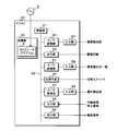
- FIG. 1 is a block diagram showing a main configuration of the power supply system 1 according to the first embodiment.
- the power supply system 1 is preferably mounted on a vehicle and includes a switch device 10, a DC power supply 11, and a load 12.
- the switch device 10 has a main switch 20 and a device connector Ta.
- the load 12 has a load connector Tb.
- the switch device 10 is connected to the positive electrode of the DC power supply 11.
- the negative electrode of the DC power supply 11 is grounded.
- the device connector Ta is detachably connected to the load connector Tb. By connecting the load connector Tb to the device connector Ta, the load 12 is connected to the device connector Ta.
- the DC power supply 11 is, for example, a battery.
- the load 12 is, for example, an electric device brought into a vehicle and has a resistance component. When the electric power supplied to the load 12 is equal to or more than a certain electric power, the load 12 operates. The constant power is a value exceeding zero W. If the power supplied to the load 12 is less than a certain amount, the load 12 stops operating.
- the DC power supply 11 supplies power to the load 12 via the main switch 20 and the device connector Ta. At this time, the electric power supplied to the load 12 is equal to or higher than a certain electric power, and the load 12 operates. In the same case, when the main switch 20 is switched from on to off, the power supplied to the load 12 by the DC power supply 11 is reduced to less than a certain power, and the load 12 stops operating.
- An operation signal instructing the operation of the load 12 and a stop signal instructing the stop of the operation of the load 12 are input to the switch device 10.
- the switch device 10 switches the main switch 20 on and operates the load 12.
- a stop signal is input, the switch device 10 switches the main switch 20 off and stops the operation of the load 12.
- the switch device 10 When a load 12 through which an overcurrent may flow is connected to the device connector Ta, the switch device 10 does not show a notification signal indicating that power cannot be supplied to the load 12. Output to. When an operation signal is input to the switch device 10 when the load 12 is not connected to the device connector Ta, the switch device 10 outputs a notification signal indicating that the load 12 is not connected to a device (not shown).
- the switch device 10 includes a current output circuit 21, a power supply detection unit 22, a microcomputer (hereinafter referred to as a microcomputer) 23, a drive circuit 24, a current resistor 25, a switch circuit 26, and a changeover switch 27. It has a switch resistor 28, a circuit resistor 29, a capacitor 30, and a voltage detection unit 31.
- the switch circuit 26 has a sub switch 40 and switch resistors 41 and 42.
- the main switch 20 is an N-channel type FET (Field Effect Transistor).
- the changeover switch 27 is an NPN type bipolar transistor.
- the sub switch 40 is a P-channel type FET.
- the drain of the main switch 20 is connected to the positive electrode of the DC power supply 11.
- the source of the main switch 20 is connected to the current output circuit 21.
- the current output circuit 21 is further connected to the device connector Ta.
- the device connector Ta is grounded.
- the drain of the main switch 20 is further connected to the power supply detection unit 22.
- the power supply detection unit 22 is connected to the microcomputer 23.
- the gate of the main switch 20 is connected to the drive circuit 24.
- the drive circuit 24 is further connected to the microcomputer 23.
- the current output circuit 21 is further connected to one end of the current resistor 25. The other end of the current resistor 25 is grounded. The connection node between the current output circuit 21 and the current resistor 25 is connected to the microcomputer 23 and the drive circuit 24.
- the drain of the main switch 20 is further connected to the source of the sub switch 40 of the switch circuit 26.
- the drain of the subswitch 40 is connected to the connection node between the current output circuit 21 and the device connector Ta.
- a switch resistor 41 is connected between the source and the gate of the sub switch 40.
- the gate of the subswitch 40 is further connected to one end of the switch resistor 42.
- the other end of the switch resistor 42 is connected to the collector of the changeover switch 27.
- the emitter of the changeover switch 27 is grounded.
- the base of the changeover switch 27 is connected to one end of the switch resistor 28.
- the other end of the switch resistor 28 is connected to the microcomputer 23.
- the drain of the main switch 20 is further connected to one end of the circuit resistor 29.
- the other end of the circuit resistor 29 is connected to a connection node between the current output circuit 21 and the device connector Ta.
- This connection node is further connected to one end of the capacitor 30 and the voltage detection unit 31.
- the other end of the capacitor 30 is grounded.
- the voltage detection unit 31 is connected to the microcomputer 23.
- the power supply detection unit 22 detects the voltage of the DC power supply 11 with reference to the ground potential. In the following, the voltage of the DC power supply 11 based on the ground potential will be referred to as a power supply voltage.
- the power supply detection unit 22 outputs power supply voltage information indicating the detected power supply voltage to the microcomputer 23.
- the power supply voltage information is an analog value, for example, a voltage proportional to the detected power supply voltage.
- the DC power supply 11 supplies power to one or more second loads (not shown) in addition to the load 12.
- the positive electrode of the DC power supply 11 is connected not only to the switch device 10 but also to one or more second loads.
- the power supply voltage of the DC power supply 11 fluctuates according to the current flowing from the DC power supply 11. The larger the current flowing from the DC power supply 11, the lower the power supply voltage.
- the main switch 20 when the gate voltage based on the source potential is a certain voltage or more, the resistance value between the drain and the source is sufficiently small. At this time, the main switch 20 is on, and current can flow through the drain and the source. In the main switch 20, when the gate voltage with respect to the source potential is less than a constant voltage, the resistance value between the drain and the source is sufficiently large. At this time, the main switch 20 is off, and no current flows through the drain and the source.
- An operation signal and a stop signal are input to the microcomputer 23.
- an ON instruction for switching the main switch 20 to ON is output to the drive circuit 24.
- the drive circuit 24 raises the voltage of the gate of the main switch 20 with reference to the ground potential. As a result, in the main switch 20, the voltage of the gate with respect to the source becomes a constant voltage or more, and the main switch 20 is switched on.
- the microcomputer 23 When the stop signal is input to the microcomputer 23, the microcomputer 23 outputs an off instruction instructing the main switch 20 to be turned off to the drive circuit 24.
- the off instruction When the off instruction is input to the drive circuit 24, the voltage of the gate with reference to the ground potential is lowered in the main switch 20. As a result, in the main switch 20, the gate voltage based on the potential of the source becomes less than a constant voltage, and the main switch 20 is switched off. As described above, the drive circuit 24 switches the main switch 20 on or off.
- the load 12 When the load 12 is connected to the device connector Ta, when the main switch 20 is on, the current flows from the positive electrode of the DC power supply 11 in the order of the main switch 20, the current output circuit 21, the device connector Ta, and the load 12. Flows. As a result, the load 12 operates.
- the current that flows from the DC power supply 11 to the main switch 20 and the current output circuit 21 in this order and is output from one end of the current output circuit 21 on the device connector Ta side is referred to as a switch current.
- the current path of the current flowing in this order from the positive electrode of the DC power supply 11 to the main switch 20, the current output circuit 21, and the device connector Ta corresponds to the first current path.
- a main switch 20 is provided in the first current path.
- the current output circuit 21 When the switch current flows, the current output circuit 21 outputs a current that is a predetermined fraction of the switch current to the current resistor 25.
- the current output circuit 21 includes, for example, a current mirror circuit.
- the predetermined number is, for example, 1000.
- the voltage between both ends of the current resistor 25 is input to the microcomputer 23 and the drive circuit 24 as current information.
- the switch current, the resistance value of the current resistance 25, and the predetermined number are described as Is, rc, and N, respectively.
- the voltage between both ends of the current resistor 25 is calculated by Is ⁇ rc / N. " ⁇ " Represents a product.
- the resistance value rc and the predetermined number N are constant values. Therefore, the voltage between both ends of the current resistor 25 is proportional to the switch current Is, and the current information indicates the switch current Is.
- the switch current does not flow regardless of whether the main switch 20 is on or not. Further, even when the main switch 20 is off, the switch current does not flow.
- the current output circuit 21 does not output the current to the current resistor 25, and zero V is input to the microcomputer 23 and the drive circuit 24 as current information.
- the drive circuit 24 switches the main switch 20 off regardless of the signal input from the microcomputer 23. After switching the main switch 20 off, the drive circuit 24 keeps the main switch 20 off regardless of the input current information.
- the cutoff threshold is a constant value and is preset.
- the changeover switch 27 when the base voltage based on the potential of the emitter is a certain voltage or more, the resistance value between the collector and the emitter is sufficiently small. At this time, the changeover switch 27 is on, and current can flow through the collector and the emitter. For the changeover switch 27, when the base voltage based on the potential of the emitter is less than a constant voltage, the resistance value between the collector and the emitter is sufficiently large. At this time, the changeover switch 27 is off, and no current flows through the collector and the emitter.
- the microcomputer 23 raises the base voltage of the changeover switch 27 with reference to the ground potential. As a result, in the changeover switch 27, the base voltage based on the potential of the emitter becomes a constant voltage or more, and the changeover switch 27 is switched on. The microcomputer 23 lowers the voltage at the base of the changeover switch 27 with reference to the ground potential. As a result, in the changeover switch 27, the base voltage based on the potential of the emitter becomes less than a constant voltage, and the changeover switch 27 is switched off. As described above, the microcomputer 23 switches the changeover switch 27 on or off.
- the sub switch 40 of the switch circuit 26 when the gate voltage based on the source potential is less than a constant voltage, the resistance value between the source and drain is sufficiently small. At this time, the sub switch 40 is on, and current can flow through the source and drain.
- the subswitch 40 of the switch circuit 26 when the gate voltage based on the source potential is a constant voltage or more, the resistance value between the source and the drain is sufficiently large. At this time, the sub switch 40 is off, and no current flows through the source and drain.
- the constant voltage for the subswitch 40 is less than zero V.
- the microcomputer 23 switches the changeover switch 27 off, the current flow through the switch resistors 41 and 42 is stopped. As a result, in the sub switch 40, the voltage of the gate based on the potential of the source rises to zero V and exceeds a constant voltage. As a result, the sub switch 40 is switched off. As described above, the microcomputer 23 switches the sub switch 40 on by switching the changeover switch 27 on, and switches the sub switch 40 off by switching the changeover switch 27 off.
- the on-resistance value of the sub-switch 40 that is, the resistance value of the switch circuit 26 when the sub-switch 40 is on is sufficiently larger than the on-resistance value of the main switch 20.
- the resistance value of the circuit resistance 29 is sufficiently larger than the on-resistance value of the subswitch 40, that is, the resistance value of the switch circuit 26 when the subswitch 40 is on.
- the on-resistance value of the main switch 20 is, for example, several ohms.
- the on-resistance value of the subswitch 40 is, for example, a resistance value belonging to the range of several hundred ohms to several kiloohms.
- the on-resistance value of an N-channel FET is usually several ohms or less. Therefore, as the sub switch 40, a P-channel type FET having a large on-resistance value is used.
- the circuit resistance is, for example, several megaohms.
- the on-resistance value of the switch is the resistance value of the switch when the switch is on.
- the voltage detection unit 31 detects the voltage of the connection node between the current output circuit 21 and the device connector Ta.
- the voltage of the connection node between the current output circuit 21 and the device connector Ta will be referred to as a node voltage.
- the node voltage is a voltage based on the ground potential.
- the voltage detection unit 31 outputs node voltage information indicating the detected node voltage to the microcomputer 23.
- the node voltage information is an analog value and indicates, for example, a voltage proportional to the node voltage.
- the microcomputer 23 determines whether or not the load 12 is connected to the device connector Ta based on the node voltage information acquired from the voltage detection unit 31 with the main switch 20 and the sub switch 40 turned off.
- the microcomputer 23 determines that the load 12 is connected to the device connector Ta, the power supply acquired from the power supply detection unit 22 and the voltage detection unit 31 with the main switch 20 turned off and the sub switch 40 turned on.
- the resistance component value of the load 12 is calculated based on the voltage information and the node voltage information.
- the microcomputer 23 determines whether or not the switch current that flows when the main switch 20 is switched on is less than the current threshold value.
- the current threshold is a constant value and is preset. The current threshold is less than the above-mentioned cutoff threshold.
- the microcomputer 23 switches the main switch 20 on or off according to the input signal.
- an operation signal is input. If so, the notification signal is output.
- FIG. 2 is a timing chart showing an operation example of the switch device 10.
- FIG. 2 shows the transition of the states of the main switch 20 and the sub switch 40 and the transition of the node voltage. Time is shown on the horizontal axis for these transitions.
- Vb indicates a power supply voltage.
- V1 indicates a first voltage dividing voltage obtained by dividing the power supply voltage Vb by the switch circuit 26 and the load 12 when the sub switch 40 is on.
- V2 indicates a second voltage dividing voltage obtained by dividing the power supply voltage Vb by the circuit resistor 29 and the load 12.
- FIG. 2 shows an operation example of the switch device 10 when the power supply voltage Vb is stable.
- Vth is a voltage threshold value for determining whether or not the load connector Tb is connected to the device connector Ta.
- the voltage threshold Vth is less than the power supply voltage Vb and exceeds the second voltage dividing voltage V2.
- the resistance component value of the load 12 is sufficiently smaller than the resistance value of the circuit resistance 29.
- a load having a resistance component value of, for example, several kilohms or less is assumed.
- the resistance value of the circuit resistor 29 is, for example, several megaohms. Therefore, the second voltage dividing voltage V2 is a value close to zero V.
- the main switch 20 and the sub switch 40 are off, when the load 12 is not connected to the device connector Ta, current flows from the positive electrode of the DC power supply 11 in the order of the circuit resistor 29 and the capacitor 30. As a result, the node voltage, that is, the voltage between both ends of the capacitor 30, is charged until the power supply voltage Vb is reached. Therefore, when the load 12 is not connected to the device connector Ta, the node voltage detected by the voltage detection unit 31 substantially matches the power supply voltage Vb and is equal to or higher than the voltage threshold value Vth. When the main switch 20 and the sub switch 40 are off and the node voltage is equal to or higher than the voltage threshold Vth, the microcomputer 23 determines that the device connector Ta is not connected to the load connector Tb.
- the capacitance of the capacitor 30 is small. Therefore, when the capacitor 30 is charged, the rate at which the node voltage rises is high. When the capacitor 30 is discharged, the rate at which the node voltage drops is also high.
- the capacitor 30 discharges through the load 12 until the node voltage becomes the second voltage dividing voltage V2. ..
- the node voltage is less than the voltage threshold Vth.
- the microcomputer 23 determines that the load 12 is connected to the device connector Ta.
- the resistance value of the circuit resistor 29 is sufficiently large. Therefore, when the main switch 20 and the sub switch 40 are off, the current flowing through the load 12 is small. Therefore, the electric power supplied to the load 12 is less than a constant electric power, and the load 12 does not operate.
- the microcomputer 23 determines that the load 12 is connected to the device connector Ta
- the microcomputer 23 switches the sub switch 40 on.
- current flows from the positive electrode of the DC power supply 11 in the order of the sub switch 40, the device connector Ta, and the load 12.
- the current path of the current flowing in this order from the positive electrode of the DC power supply 11 to the sub switch 40 and the device connector Ta corresponds to the second current path.
- a sub switch 40 that is, a switch circuit 26 is provided in the second current path.
- the connection node between the current output circuit 21 and the device connector Ta is a connection node on the downstream side of the main switch 20 and the sub switch 40.
- the resistance value of the circuit resistor 29 is sufficiently larger than the on-resistance value of the subswitch 40. Therefore, when the sub switch 40 is on, the current flowing through the circuit resistor 29 is substantially zero A. Further, since the resistance value of the switch circuit 26 when the sub switch 40 is on, that is, the on resistance value of the sub switch 40 is large, the current flowing through the load 12 is small. Therefore, the power supplied to the load 12 is less than a constant power, and the load 12 does not operate.
- the resistance value of the switch circuit 26 is large when the sub switch 40 is on, the load 12 having a resistance component value of zero ohm is connected to the device connector Ta, and the main switch 20 and the sub switch 40 are each off. And when it is on, the current that flows is small. This current is a normal value that does not cause smoke in the connection line connecting the sub switch 40, the DC power supply 11 and the sub switch 40, or the connection line connecting the sub switch 40 and the device connector Ta.
- the current flowing when the load 12 having a resistance component value of zero ohm is connected to the device connector Ta and the main switch 20 and the sub switch 40 are off and on, respectively, raises the temperature of the sub switch 40 to an abnormal temperature. I won't let you. Therefore, the sub switch 40 does not fail.
- zero ohm is not an exact value, but a substantial value.
- the node voltage of the DC power supply 11 becomes the first voltage dividing voltage V1.
- the resistance component value of the load 12 is calculated based on the pressure voltage V1.
- the resistance value of the switch circuit 26 when the sub switch 40 is on is described as rs.
- the resistance component value of the load 12 is described as rd.
- the first voltage dividing voltage V1 is represented by the following equation using the resistance value rs, the resistance component value rd, and the power supply voltage Vb.
- V1 Vb ⁇ (rd / (rs + rd))
- the resistance value rs of the switch circuit 26 has been measured in advance and is a known value.
- the power supply voltage Vb and the first voltage dividing voltage V1 are detected by the power supply detection unit 22 and the voltage detection unit 31, respectively. Therefore, the resistance value rs of the switch circuit 26 can be calculated.
- the microcomputer 23 switches the sub switch 40 off after acquiring the node voltage information indicating the first voltage dividing voltage V1. As a result, the capacitor 30 is discharged until the node voltage becomes the second voltage dividing voltage V2.
- the microcomputer 23 determines whether or not the switch current that flows when the main switch 20 is switched on, that is, Vb / rs is less than the current threshold value. When the microcomputer 23 determines that the switch current is equal to or greater than the current threshold value, the microcomputer 23 outputs a notification signal indicating that power cannot be supplied to the load 12. When the microcomputer 23 determines that the switch current is less than the current threshold value, the microcomputer 23 executes a power supply control process for controlling the power supply to the load 12. In the power supply control process, the microcomputer 23 switches the main switch 20 on or off based on the input signal. The subswitch 40 is kept off while the power supply control process is being executed.
- the main switch 20 when the main switch 20 is on, power is supplied to the load 12 and the load 12 operates. Since the on-resistance value of the main switch 20 is sufficiently smaller than the resistance value of the circuit resistance 29, the current flowing through the circuit resistance 29 when the main switch 20 is on is substantially zero A.
- the capacitor 30 When the main switch 20 is on, the capacitor 30 is charged until the node voltage reaches the power supply voltage Vb.
- the main switch 20 When the main switch 20 is off, the capacitor 30 discharges until the node voltage reaches the second voltage dividing voltage V2.
- the microcomputer 23 periodically determines whether or not the load 12 is connected to the device connector Ta while executing the power supply control process. When the main switch 20 is off, the microcomputer 23 determines whether or not the node voltage is equal to or higher than the voltage threshold voltage Vth because the node voltage is the power supply voltage Vb.
- the switch current flows when the load 12 is connected to the device connector Ta.
- the switch current does not flow, and the switch current indicated by the current information input to the microcomputer 23 is zero A.
- the microcomputer 23 determines whether or not the load 12 is connected to the device connector Ta based on the input current information.
- FIG. 3 is a block diagram showing a main configuration of the microcomputer 23.
- the microcomputer 23 has an A / D conversion unit 50, 51, 52, an output unit 53, 54, a switching unit 55, an input unit 56, 57, 58, 59, a storage unit 60, and a control unit 61.
- the A / D conversion units 50, 51, 52, the output units 53, 54, the switching unit 55, the input unit 56, the storage unit 60, and the control unit 61 are connected to the internal bus 62.
- the A / D conversion units 50, 51, and 52 are further connected to the input units 57, 58, and 59, respectively.
- Each of the input units 57, 58, and 59 is connected to the power supply detection unit 22, one end of the current resistor 25, and the voltage detection unit 31.
- the output unit 53 is further connected to the drive circuit 24.
- the switching unit 55 is connected to the base of the switching switch 27 via a switch resistor 28.
- Analog power supply voltage information is input from the power supply detection unit 22 to the input unit 57.
- the input unit 57 outputs the input analog power supply voltage information to the A / D conversion unit 50.
- the A / D conversion unit 50 converts the analog power supply voltage information input from the input unit 57 into digital power supply voltage information.
- the control unit 61 acquires digital power supply voltage information from the A / D conversion unit 50.
- the power supply voltage indicated by the power supply voltage information acquired by the control unit 61 substantially matches the power supply voltage detected by the power supply detection unit 22 at the time of acquisition.
- the output unit 53 outputs an on instruction and an off instruction to the drive circuit 24 according to the instruction of the control unit 61.
- the drive circuit 24 switches the main switch 20 on when an on instruction is input, and switches the main switch 20 off when an off instruction is input.
- Analog current information is input to the input unit 58 from one end of the current resistor 25.
- the input unit 58 outputs the input analog current information to the A / D conversion unit 51.
- the A / D conversion unit 51 converts the analog current information input from the input unit 58 into digital current information.
- the control unit 61 acquires digital current information from the A / D conversion unit 51.
- the switch current indicated by the current information acquired by the control unit 61 substantially matches the switch current detected at the time of acquisition.
- the control unit 61 instructs the switching unit 55 to switch the sub switch 40 on or off.
- the switching unit 55 raises the base voltage of the changeover switch 27 with reference to the ground potential and switches the changeover switch 27 on.
- the control unit 61 instructs the sub switch 40 to switch off
- the switching unit 55 lowers the voltage of the base of the changeover switch 27 with reference to the ground potential, and switches the changeover switch 27 to off.
- the changeover switch 27 is switched off, the sub switch 40 is switched off.
- Analog node voltage information is input from the voltage detection unit 31 to the input unit 59.
- the input unit 59 outputs the input analog node voltage information to the A / D conversion unit 52.
- the A / D conversion unit 52 converts the analog node voltage information input from the input unit 59 into digital node voltage information.
- the control unit 61 acquires digital node voltage information from the A / D conversion unit 52.
- the node voltage indicated by the node voltage information acquired by the control unit 61 substantially matches the node voltage detected by the power supply detection unit 22 at the time of acquisition.
- the operation signal and the stop signal are input to the input unit 56.
- the input unit 56 notifies the control unit 61 of the input signal.
- the output unit 54 outputs a notification signal according to the instruction of the control unit 61.
- the storage unit 60 is a non-volatile memory.
- the computer program P is stored in the storage unit 60.
- the control unit 61 has a processing element for executing processing, for example, a CPU (Central Processing Unit), and functions as a processing unit.
- the processing element (computer) of the control unit 61 executes the connection detection process, the current determination process, and the power supply control process described above in parallel.
- the connection detection process is a process for detecting the connection of the load 12 to the device connector Ta.
- the current determination process is a process for determining whether or not the switch current that flows when the main switch 20 is turned on is less than the current threshold value.
- the processing element included in the control unit 61 may be readablely stored in the storage medium E.
- the computer program P read from the storage medium E by a reading device (not shown) is written in the storage unit 60.
- the storage medium E is an optical disk, a flexible disk, a magnetic disk, a magnetic optical disk, a semiconductor memory, or the like.
- the optical disk is a CD (Compact Disc) -ROM (Read Only Memory), a DVD (Digital Versatile Disc) -ROM, or a BD (Blu-ray (registered trademark) Disc).
- the magnetic disk is, for example, a hard disk.
- the computer program P may be downloaded from an external device (not shown) connected to a communication network (not shown), and the downloaded computer program P may be written in the storage unit 60.
- the number of processing elements included in the control unit 61 is not limited to 1, and may be 2 or more.
- the plurality of processing elements may jointly execute the connection detection process, the current determination process, and the power supply control process according to the computer program P.
- the storage unit 60 stores the values of the connection flag and the permission flag in addition to the computer program P.
- the values of the connection flag and the permission flag are zero or one, respectively.
- a value of the connection flag of zero means that the load 12 is not connected to the device connector Ta.
- the value of the connection flag is 1 it means that the load 12 is connected to the device connector Ta.
- the value of the permission flag is zero, it means that the main switch 20 is prohibited from being switched on.
- the value of the permission flag is 1, it means that the main switch 20 is allowed to be switched on.
- FIG. 4 is a flowchart showing the procedure of the connection detection process.
- the control unit 61 periodically executes the connection detection process when the sub switch 40 is off.
- the control unit 61 determines whether or not the main switch 20 is off (step S1).
- step S1 when the latest instruction output by the output unit 53 is an off instruction, the control unit 61 determines that the main switch 20 is off.
- the control unit 61 determines that the main switch 20 is on.
- control unit 61 determines that the main switch 20 is off (S1: YES)
- the control unit 61 acquires node voltage information from the A / D conversion unit 52 (step S2).
- the control unit 61 determines whether or not the load 12 is connected to the device connector Ta based on the node voltage indicated by the node voltage information acquired in step S2 (step S3).
- the control unit 61 determines that the load 12 is not connected when the node voltage is equal to or higher than the voltage threshold value.
- the control unit 61 determines that the load 12 is connected.
- step S4 When the control unit 61 determines that the load 12 is connected (S3: YES), the control unit 61 sets the value of the connection flag to 1 (step S4), and ends the connection detection process. If the value of the connection flag is 1 when it is determined that the control unit 61 and the load 12 are connected, the execution of step S4 is omitted, and the connection detection process ends.
- control unit 61 determines that the load 12 is not connected (S3: NO)
- the control unit 61 sets the value of the connection flag to zero (step S5), and ends the connection detection process. If the value of the connection flag is zero when the load 12 is determined not to be connected, the control unit 61 omits the execution of step S5 and ends the connection detection process.
- step S6 When the control unit 61 determines that the main switch 20 is not off, that is, the main switch 20 is on (S1: NO), the control unit 61 acquires current information from the A / D conversion unit 51 (step S6). Next, the control unit 61 determines whether or not the load 12 is connected to the device connector Ta based on the switch current indicated by the current information acquired in step S6 (step S7). As described in the operation example of the switch device 10, in step S7, when the switch current exceeds zero A, the control unit 61 determines that the load 12 is connected. When the switch current is zero A, the control unit 61 determines that the load 12 is not connected.
- the output unit 53 does not output the ON instruction to the drive circuit 24. Therefore, the drive circuit 24 switches the main switch 20 on while the value of the connection flag is 1. When the main switch 20 is on, the value of the connection flag is 1. The value of the connection flag is 1 when step S7 is executed.
- control unit 61 determines that the load 12 is not connected (S7: NO)
- the control unit 61 instructs the output unit 53 to switch the main switch 20 off (step S8).
- the output unit 53 switches the main switch 20 off by outputting an off instruction to the drive circuit 24.
- the control unit 61 sets the value of the connection flag to zero (step S9).
- the control unit 61 ends the connection detection process when it determines that the load 12 is connected (S7: YES) or after executing step S9.
- the control unit 61 detects the connection of the load 12 based on the node voltage when the main switch 20 is off, and based on the switch current when the main switch 20 is on. Detects the connection of the load 12.
- the drive circuit 24 switches the main switch 20 off, and the control unit 61 sets the value of the connection flag to zero. If the load 12 and the device connector Ta are disconnected while the load 12 is operating, the state of the switch device 10 is that the load 12 is not connected even though the main switch 20 is on. Become.
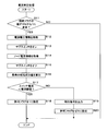
- FIG. 5 is a flowchart showing the procedure of the current determination process.
- the control unit 61 periodically executes the current determination process when the main switch 20 is off.
- the control unit 61 determines whether or not the value of the connection flag has been changed from zero to 1, that is, whether or not the load 12 is connected to the device connector Ta (step S11).
- step S11 when the value of the connection flag, which was zero at the start of the previous current determination process, is changed to 1, the control unit 61 determines that the value of the connection flag has been changed from zero to 1.
- control unit 61 determines that the value of the connection flag has not been changed from zero to one (S11: NO)
- the control unit 61 ends the current determination process.
- the control unit 61 executes the current determination process again. Therefore, when the control unit 61 determines that the value of the connection flag has not been changed from zero to 1, it waits until the value of the connection flag is changed from zero to one.
- control unit 61 determines that the value of the connection flag is changed from zero to 1, that is, the load 12 is connected to the device connector Ta (S11: YES), the control unit 61 outputs the power supply voltage information from the A / D conversion unit 50. Acquire (step S12). Next, the control unit 61 instructs the switching unit 55 to switch the sub switch 40 on (step S13). As described above, the switching unit 55 switches the sub switch 40 on by switching the switching switch 27 on. When the sub switch 40 is switched on, the capacitor 30 is charged until the node voltage becomes the first voltage dividing voltage.
- step S14 the control unit 61 acquires node voltage information from the A / D conversion unit 52 (step S14).
- the period from the end of the execution of step S13 to the start of the execution of step S14 is longer than the period from when the sub switch 40 is switched on to when the charging of the capacitor 30 is completed. Therefore, the node voltage indicated by the node voltage information acquired by the control unit 61 in step S14 is the first voltage dividing voltage.
- step S15 the control unit 61 instructs the switching unit 55 to switch the sub switch 40 off (step S15).
- the switching unit 55 switches the sub switch 40 off by switching the switching switch 27 off.
- the capacitor 30 is discharged and the node voltage drops to the second voltage dividing voltage.
- step S15 the control unit 61 calculates the resistance component value of the load 12 based on the node voltage indicated by the node voltage information acquired in step S14, that is, the first voltage dividing voltage (step S16). Next, the control unit 61 determines whether or not the switch current flowing when the main switch 20 is switched on is less than the current threshold value based on the resistance component value calculated in step S16 (step S17). ..
- step S17 the control unit 61 calculates the switch current based on the power supply voltage indicated by the power supply voltage information acquired in step S12 and the resistance component value calculated in step S16. The control unit 61 determines whether or not the calculated switch voltage is less than the current threshold value.
- step S17 when the resistance component value calculated in step S16 is equal to or greater than the resistance threshold value, the control unit 61 determines that the switch current is less than the current threshold value. When the resistance component value calculated in step S16 is less than the resistance threshold value, the control unit 61 determines that the switch current is equal to or more than the current threshold value.
- the resistance threshold is a constant value and is preset.
- control unit 61 determines that the switch current is less than the current threshold value (S17: YES)
- the control unit 61 sets the value of the permission flag to 1 (step S18), and ends the current determination process.
- the control unit 61 determines that the switch current is equal to or greater than the current threshold value (S17: NO)
- the control unit 61 instructs the output unit 54 to output a notification signal indicating that power supply to the load 12 is impossible (S17: NO). Step S19).
- the control unit 61 sets the value of the permission flag to zero (step S20), and ends the current determination process.
- the resistance component value of the load 12 is calculated, and whether or not the switch current is less than the current threshold value based on the calculated resistance component value. Is determined.
- the control unit 61 determines that the switch current is less than the current threshold value, the control unit 61 sets the value of the permission flag to 1 and permits the main switch 20 to be switched on.
- FIG. 6 is a flowchart showing the procedure of the power supply control process.
- the control unit 61 periodically executes the power supply control process when the sub switch 40 is off.
- the control unit 61 determines whether or not an operation signal has been input to the input unit 56 (step S31).
- the control unit 61 determines whether or not a stop signal has been input to the input unit 56 (step S32).
- the control unit 61 ends the power supply control process.
- the control unit 61 executes the power supply control process again. Therefore, when the operation signal or the stop signal is not input to the input unit 56, the control unit 61 waits until the operation signal or the stop signal is input to the input unit 56.
- control unit 61 determines whether or not the value of the connection flag is 1 (step S33).
- control unit 61 determines whether or not the value of the permission flag is 1 (step S34).
- control unit 61 instructs the output unit 53 to turn on the main switch 20 (step S35).
- the output unit 53 switches the main switch 20 on by outputting an ON instruction to the drive circuit 24. As a result, the load 12 operates.
- the control unit 61 determines that the value of the connection flag is not 1 (S33: NO) or determines that the value of the permission flag is not 1 (S34: NO), the control unit 61 instructs the output unit 54.
- the notification signal is output (step S36). If the value of the connection flag is not 1, the output unit 54 outputs a notification signal indicating that the load 12 is not connected. If the value of the permission flag is not 1, the output unit 54 outputs a notification signal indicating that power cannot be supplied to the load 12.
- steps S35 and S36 is executed, the control unit 61 ends the power supply control process.
- step S37 the control unit 61 instructs the output unit 53 to switch the main switch 20 off.
- the output unit 53 switches the main switch 20 off by outputting an off instruction to the drive circuit 24.
- the load 12 stops operating.
- step S37 the control unit 61 ends the power supply control process.
- the control unit 61 instructs the output unit 53 to switch the main switch 20 on.
- the value of the permission flag is zero, the control unit 61 does not instruct the output unit 53 to switch the main switch 20 on. Therefore, the passage of an overcurrent exceeding the current threshold value is prevented.
- the control unit 61 instructs the output unit 53 to switch the main switch 20 off.
- FIG. 7 is a block diagram showing a main configuration of the microcomputer 23 according to the second embodiment.
- the microcomputer 23 in the second embodiment has a clock signal output unit 63 in addition to the components included in the microcomputer 23 in the first embodiment.
- the clock signal output unit 63 is connected to the internal bus 62 and directly connected to the control unit 61.
- the clock signal output unit 63 outputs a clock signal to the control unit 61.
- the clock signal is composed of a high level voltage and a low level voltage.
- the voltage indicated by the clock signal periodically switches from the low level voltage to the high level voltage.
- the processing element of the control unit 61 executes one process each time the voltage is switched from the low level voltage to the high level voltage in the clock signal.
- the control unit 61 stops the output of the clock signal to the clock signal output unit 63 via the internal bus 62.
- the processing element of the control unit 61 stops operating.
- the operation signal and stop signal are input not only to the input unit 56 but also to the clock signal output unit 63.
- the clock signal output unit 63 restarts the output of the clock signal to the control unit 61.
- the processing element of the control unit 61 resumes operation.
- the processing element of the control unit 61 executes not only the connection detection process, the current determination process, and the power supply control process, but also the pause process and the start process.
- the pause process is a process of stopping the output of the clock signal.
- the start-up process is the first process to be executed when the control unit 61 resumes operation.
- FIG. 8 is a flowchart showing the procedure of the pause process.
- the control unit 61 periodically executes the pause process.
- the control unit 61 determines whether or not to pause the operation (step S41).
- the control unit 61 determines that the operation is suspended when the off period in which the main switch 20 and the sub switch 40 are off is equal to or longer than the reference period. When the off period is less than the reference time, the control unit 61 determines that the operation is not paused.
- control unit 61 determines that the operation is not paused (S41: NO)
- the control unit 61 ends the pause processing.
- the control unit 61 executes the pause process. Therefore, when the control unit 61 determines that the operation is not paused, the control unit 61 waits until the off period becomes equal to or longer than the reference period.
- the control unit 61 determines that the operation is suspended (S41: YES)
- the control unit 61 instructs the clock signal output unit 63 to stop the output of the clock signal to the control unit 61 (step S42), and ends the pause process. ..
- the control unit 61 suspends the operation. If an operation signal or a stop signal is input to the clock signal output unit 63 after the control unit 61 has stopped operating, the clock signal output unit 63 resumes the output of the clock signal, and the control unit 61 resumes the operation. ..
- FIG. 9 is a flowchart showing the procedure of the start-up process.
- the control unit 61 executes the start-up process when the operation is restarted, that is, when the output of the clock signal is restarted. Since the control unit 61 pauses in a state where the main switch 20 and the sub switch 40 are off, the start-up process is executed in a state where the main switch 20 and the sub switch 40 are off. A part of the start-up process is the same as a part of the current determination process. Therefore, regarding the start-up process, a process similar to a part of the current determination process, that is, the description of steps S12 to S20 will be omitted.
- the control unit 61 acquires the node voltage information from the A / D conversion unit 52 (step S51). Next, the control unit 61 determines whether or not the load 12 is connected to the device connector Ta based on the node voltage indicated by the node voltage information acquired in step S51, as in step S3 of the connection detection process. (Step S52).
- control unit 61 determines that the load 12 is not connected (S52: NO)
- the control unit 61 sets the value of the connection flag to zero (step S53), and ends the start-up process.
- the control unit 61 determines that the load 12 is connected (S52: YES)
- the control unit 61 sets the value of the connection flag to 1 (step S54).
- step S54 the control unit 61 sequentially executes steps S12 to S16 to calculate the resistance component value of the load 12. Based on the calculated resistance component value, the control unit 61 determines whether or not the switch current that flows when the main switch 20 is switched on is less than the current threshold value. The control unit 61 sets the value of the permission flag to zero or one according to the determination result.
- the control unit 61 ends the start-up process after executing one of steps S18 and S20. After finishing the start-up process, the control unit 61 executes the connection detection process, the current determination process, the power supply control process, and the pause process.
- the control unit 61 determines whether or not the load 12 is connected to the device connector Ta.
- the control unit 61 calculates the resistance component value of the load 12, and based on the calculated resistance component value, the switch current that flows when the main switch 20 is switched on. Determines if is less than the current threshold. Therefore, when the electric device connected to the device connector Ta is changed to the electric device having a small resistance component value as the load 12 while the control unit 61 is inactive, the control unit 61 is erroneously used. Therefore, the output unit 53 is not instructed to switch the main switch 20 on.
- the switch device 10 according to the second embodiment similarly exhibits the effect of the switch device 10 according to the first embodiment.
- control unit 61 may omit step S12 in the current determination process in the first and second embodiments. In this case, in step S16, the control unit 61 uses a preset value as the power supply voltage.
- step S17 of the current determination process in the first and second embodiments the control unit 61 determines whether or not the switch current is less than the current threshold value based on the resistance component value calculated in step S16. However, in step S17, the control unit 61 directly determines whether or not the switch current is less than the current threshold value based on the node voltage indicated by the node voltage information acquired in step S14, that is, the first voltage dividing voltage. You may. As described above, the switch current that flows when the main switch 20 is switched on increases as the resistance component value of the load 12 decreases. The resistance component value of the load 12 becomes smaller as the first voltage dividing voltage is lower. Therefore, the lower the first voltage dividing voltage, the larger the switch current.
- step S17 the control unit 61 determines that the switch current is equal to or greater than the current threshold value when the node voltage indicated by the node voltage information acquired in step S14 is less than the reference voltage.
- the control unit 61 determines that the switch current is less than the current threshold value.
- the first voltage dividing voltage is proportional to the power supply voltage of the DC power supply 11. Therefore, the reference voltage used in step S17 is changed according to the power supply voltage indicated by the power supply voltage information acquired in step S12.
- control unit 61 does not need to change the reference voltage. In this case, in the current determination process, the control unit 61 may omit step S12. Further, the switch device 10 does not need to have the power supply detection unit 22, and the microcomputer 23 does not need to have the A / D conversion unit 50 and the input unit 57.
- the control unit 61 may omit the execution of step S12 as in the current determination process. Further, in step S17 of the start-up process, the control unit 61 performs the switch current based on the node voltage indicated by the node voltage information acquired in step S14, that is, the first voltage dividing voltage, as in step S17 of the current determination process. May be directly determined whether or not is less than the current threshold.
- the method of stopping the operation of the control unit 61 is not limited to the method of stopping the output of the clock signal.
- the period of the clock signal output by the clock signal output unit 63 to the control unit 61 that is, the interval at which the low level voltage is switched to the high level voltage is described as the first period.
- the control unit 61 operates by instructing the clock signal output unit 63 to change the cycle of the clock signal output to the control unit 61 from the first cycle to the second cycle longer than the first cycle. May be paused.
- the operation signal and the stop signal are not input to the clock signal output unit 63.
- the control unit 61 determines whether or not an operation signal or a stop signal is input to the input unit 56 each time the clock signal voltage is switched from the low level voltage to the high level voltage while the clock signal cycle is the second cycle. judge.
- the control unit 61 instructs the clock signal output unit 63 to change the clock signal cycle to the first cycle and execute the start processing.
- the clock signal is not limited to a signal in which the voltage periodically switches from the low level voltage to the high level voltage, and may be a signal in which the voltage periodically switches from the high level voltage to the low level voltage.
- the processing element of the control unit 61 executes processing each time the voltage is switched from the high level voltage to the low level voltage in the clock signal.
- the subswitch 40 of the switch circuit 26 is not limited to the P-channel type FET.
- the third embodiment will be described as different from the first embodiment.
- Other configurations except the configuration described later are common to the first embodiment. Therefore, the same reference reference numerals as those in the first embodiment are assigned to the components common to the first embodiment, and the description thereof will be omitted.
- FIG. 10 is a block diagram showing a main configuration of the switch device 10 according to the third embodiment.
- the switch device 10 according to the third embodiment also has other components other than the changeover switch 27 and the switch resistor 28 among the components included in the switch device 10 according to the first embodiment.
- the switch device 10 in the third embodiment further includes a drive circuit 32.
- the switch circuit 26 in the third embodiment has a series resistor 43 in addition to the components of the switch circuit 26 in the first embodiment.
- the sub-switch 40 in the third embodiment is an N-channel type FET.
- the drain of the sub switch 40 of the switch circuit 26 is connected to the drain of the main switch 20.
- the source of the subswitch 40 is connected to one end of the series resistor 43.
- the series resistor 43 functions as a second resistor.
- the other end of the series resistor 43 is connected to a connection node between the current output circuit 21 and the device connector Ta.
- a switch resistor 41 is connected between the gate and the source of the sub switch 40.
- the gate of the subswitch 40 is further connected to one end of the switch resistor 42.
- the other end of the switch resistor 42 is connected to the drive circuit 32.
- the drive circuit 32 is further connected to the switching unit 55 of the microcomputer 23.
- the sub switch 40 when the gate voltage based on the source potential is a certain voltage or more, the resistance value between the drain and the source is sufficiently small. At this time, the sub switch 40 is on, and current can flow through the drain and the source. In the subswitch 40, when the gate voltage with respect to the source potential is less than a constant voltage, the resistance value between the drain and the source is sufficiently large. At this time, the sub switch 40 is off, and no current flows through the drain and the source.
- the switching unit 55 when the control unit 61 instructs the switching unit 55 to switch the sub switch 40 on, the switching unit 55 outputs a second on instruction instructing the sub switch 40 to switch on.
- the drive circuit 32 raises the voltage of the gate of the subswitch 40 with reference to the ground potential.
- the voltage of the gate based on the potential of the source becomes a constant voltage or more, and the sub switch 40 is switched on.
- the switching unit 55 when the control unit 61 instructs the switching unit 55 to switch the sub switch 40 to off, the switching unit 55 outputs a second off instruction instructing the switching of the sub switch 40 to off.
- the drive circuit 32 lowers the voltage at the gate of the subswitch 40 with reference to the ground potential.
- the voltage of the gate based on the potential of the source becomes less than a constant voltage, and the sub switch 40 is switched off.
- the on-resistance value of the N-channel FET is usually several ohms and is small.
- a series resistor 43 is connected in series to the sub switch 40 in order to realize a circuit having a large resistance value when the sub switch 40 is on. For example, when the resistance value of the series resistor 43 is several hundred ohms, the resistance value of the switch circuit 26 when the sub switch 40 is on is several hundred ohms.
- the resistance value of the switch circuit 26 when the sub switch 40 is on is larger than the on resistance value of the main switch 20.
- the resistance value of the circuit resistance is larger than the resistance value of the switch circuit 26 when the sub switch 40 is on.
- the current flowing when the load 12 having a resistance component value of zero ohm is connected to the device connector Ta and the main switch 20 and the sub switch 40 are off and on, respectively, is a normal value that does not cause smoke generation.
- the switch device 10 in the third embodiment similarly exhibits the effect of the switch device 10 in the first embodiment.
- the on-resistance value of the relay contact is smaller than the on-resistance value of the N-channel FET. Therefore, a relay contact may be used as the sub switch 40 in the third embodiment.
- the switch device 10 is provided with a configuration for switching the sub switch 40 on or off.
- the sub switch 40 is switched on or off by the switching unit 55.
- the source of the sub switch 40 may be connected to the connection node between the current output circuit 21 and the device connector Ta.
- one end of the series resistor 43 may be connected in series to the drain of the sub switch 40.
- the other end of the series resistor 43 is connected to the connection node between the current output circuit 21 and the device connector Ta.
- the switch device 10 in the second embodiment may be configured in the same manner as the switch device 10 in the third embodiment.
- the sub switch 40 is not limited to the FET or the relay contact, and may be a switch such as a bipolar transistor or an IGBT (Insulated Gate Bipolar Transistor).
- the configuration for detecting the switch current is not limited to the configuration in which a current that is a predetermined fraction of the switch current is output to the current resistor 25, and a configuration using a shunt resistor or a current sensor may be used.
- the shunt resistor is connected in series with the source of the main switch 20, and the switch current is detected based on the voltage between both ends of the shunt resistor.
- the current sensor detects the switch current based on the strength of the magnetic field generated when the switch current flows through the connection line connected to the source of the main switch 20.
Landscapes
- Engineering & Computer Science (AREA)
- Power Engineering (AREA)
- Direct Current Feeding And Distribution (AREA)
- Electronic Switches (AREA)
Abstract
スイッチ装置(10)の装置コネクタ(Ta)には、負荷(12)が着脱可能に接続される。サブスイッチ(40)がオンである場合におけるスイッチ回路(26)の抵抗値はメインスイッチ(20)のオン抵抗値よりも大きい。マイコン(23)は、メインスイッチ(20)がオフであり、かつ、サブスイッチ(40)がオンである状態で、メインスイッチ(20)及びサブスイッチ(40)の下流側の接続ノードのノード電圧を示すノード電圧情報を電圧検出部(31)から取得する。マイコン(23)は、取得したノード電圧情報に基づいて、メインスイッチ(20)がオンに切替わった場合にメインスイッチ(20)を介して流れるスイッチ電流が電流閾値未満であるか否かを判定する。
Description
本開示は、スイッチ装置、電流判定方法及びコンピュータプログラムに関する。
本出願は、2019年12月13日出願の日本出願第2019-225848号に基づく優先権を主張し、前記日本出願に記載された全ての記載内容を援用するものである。
本出願は、2019年12月13日出願の日本出願第2019-225848号に基づく優先権を主張し、前記日本出願に記載された全ての記載内容を援用するものである。
特許文献1には、直流電源から負荷への電流経路にスイッチが配置されている車両用のスイッチ装置が開示されている。このスイッチ装置では、スイッチをオン又はオフに切替えることによって、直流電源から負荷への給電を制御する。
本開示の一態様に係るスイッチ装置は、負荷に着脱可能に接続されるコネクタと、直流電源から前記コネクタへの第1電流経路に設けられたメインスイッチと、前記直流電源から前記コネクタへの第2電流経路に設けられ、サブスイッチを有するスイッチ回路と、処理を実行する処理部とを備え、前記サブスイッチがオンである場合における前記スイッチ回路の抵抗値は、前記メインスイッチのオン抵抗値よりも大きく、前記処理部は、前記メインスイッチがオフであり、かつ、前記サブスイッチがオンである状態で、前記メインスイッチ及びサブスイッチの下流側の接続ノードのノード電圧を示すノード電圧情報を取得し、取得したノード電圧情報に基づいて、前記メインスイッチがオンに切替わった場合に前記メインスイッチを介して流れるスイッチ電流が電流閾値未満であるか否かを判定する処理を実行する。
本開示の一態様に係る電流判定方法では、直流電源から、負荷に着脱可能に接続されるコネクタへの第1電流経路に設けられたメインスイッチがオフであり、かつ、前記直流電源から前記コネクタへの第2電流経路に設けられたスイッチ回路が有するサブスイッチがオンである状態で、前記メインスイッチ及びサブスイッチの下流側の接続ノードのノード電圧を示すノード電圧情報を取得するステップと、取得したノード電圧情報に基づいて、前記メインスイッチがオンに切替わった場合に前記メインスイッチを介して流れるスイッチ電流が電流閾値未満であるか否かを判定するステップとをコンピュータが実行し、前記サブスイッチがオンである場合における前記スイッチ回路の抵抗値は、前記メインスイッチのオン抵抗値よりも大きい。
本開示の一態様に係るコンピュータは、直流電源から、負荷に着脱可能に接続されるコネクタへの第1電流経路に設けられたメインスイッチがオフであり、かつ、前記直流電源から前記コネクタへの第2電流経路に設けられたスイッチ回路が有するサブスイッチがオンである状態で、前記メインスイッチ及びサブスイッチの下流側の接続ノードのノード電圧を示すノード電圧情報を取得するステップと、取得したノード電圧情報に基づいて、前記メインスイッチがオンに切替わった場合に前記メインスイッチを介して流れるスイッチ電流が電流閾値未満であるか否かを判定するステップとをコンピュータに実行させるために用いられ、前記サブスイッチがオンである場合における前記スイッチ回路の抵抗値は、前記メインスイッチのオン抵抗値よりも大きい。
なお、本開示を、このような特徴的な処理部を備えるスイッチ装置として実現することができるだけでなく、かかる特徴的な処理をステップとする電流判定方法として実現したり、かかるステップをコンピュータに実行させるためのコンピュータプログラムとして実現したりすることができる。また、本開示を、スイッチ装置の一部又は全部を実現する半導体集積回路として実現したり、スイッチ装置を含む電源システムとして実現したりすることができる。
[本開示が解決しようとする課題]
直流電源から負荷への電流経路にスイッチが配置されている従来のスイッチ装置として、負荷に着脱可能に接続されるコネクタを有するスイッチ装置が挙げられる。このスイッチ装置では、スイッチがオンである場合、直流電源は、スイッチ及びコネクタを介して負荷に電力を供給する。スイッチを介して流れる電流は、コネクタに接続される負荷の抵抗成分値が小さい程、大きい。コネクタに、抵抗成分値が小さい負荷がコネクタに接続された場合、スイッチを介して過電流が流れる可能性がある。
直流電源から負荷への電流経路にスイッチが配置されている従来のスイッチ装置として、負荷に着脱可能に接続されるコネクタを有するスイッチ装置が挙げられる。このスイッチ装置では、スイッチがオンである場合、直流電源は、スイッチ及びコネクタを介して負荷に電力を供給する。スイッチを介して流れる電流は、コネクタに接続される負荷の抵抗成分値が小さい程、大きい。コネクタに、抵抗成分値が小さい負荷がコネクタに接続された場合、スイッチを介して過電流が流れる可能性がある。
そこで、過電流の通流を防止することができるスイッチ装置、電流判定方法及びコンピュータプログラムを提供することを目的とする。
[本開示の効果]
本開示によれば、過電流の通流を防止することができる。
本開示によれば、過電流の通流を防止することができる。
[本開示の実施形態の説明]
最初に本開示の実施態様を列挙して説明する。以下に記載する実施形態の少なくとも一部を任意に組み合わせてもよい。
最初に本開示の実施態様を列挙して説明する。以下に記載する実施形態の少なくとも一部を任意に組み合わせてもよい。
(1)本開示の一態様に係るスイッチ装置は、負荷に着脱可能に接続されるコネクタと、直流電源から前記コネクタへの第1電流経路に設けられたメインスイッチと、前記直流電源から前記コネクタへの第2電流経路に設けられ、サブスイッチを有するスイッチ回路と、処理を実行する処理部とを備え、前記サブスイッチがオンである場合における前記スイッチ回路の抵抗値は、前記メインスイッチのオン抵抗値よりも大きく、前記処理部は、前記メインスイッチがオフであり、かつ、前記サブスイッチがオンである状態で、前記メインスイッチ及びサブスイッチの下流側の接続ノードのノード電圧を示すノード電圧情報を取得し、取得したノード電圧情報に基づいて、前記メインスイッチがオンに切替わった場合に前記メインスイッチを介して流れるスイッチ電流が電流閾値未満であるか否かを判定する処理を実行する。
(2)本開示の一態様に係るスイッチ装置では、前記処理部は、取得したノード電圧情報に基づいて前記負荷の抵抗成分値を算出し、算出した抵抗成分値に基づいて、前記メインスイッチがオンに切替わった場合に流れる前記スイッチ電流が前記電流閾値未満であるか否かを判定する処理を実行する。
(3)本開示の一態様に係るスイッチ装置は、前記直流電源から前記コネクタへの第3電流経路に設けられ、一端が前記接続ノードに接続される抵抗と、前記接続ノードに一端が接続されているキャパシタとを備え、前記処理部は、前記メインスイッチ及びサブスイッチがオフである状態で前記ノード電圧情報を取得し、前記メインスイッチ及びサブスイッチがオフである状態で取得した前記ノード電圧情報に基づいて前記負荷が前記コネクタに接続されているか否かを判定する処理を実行する。
(4)本開示の一態様に係るスイッチ装置では、前記処理部は、前記負荷が前記コネクタに接続されたと判定した場合、前記メインスイッチがオフであり、かつ、前記サブスイッチがオンである状態で前記ノード電圧情報を取得する処理を実行する。
(5)本開示の一態様に係るスイッチ装置では、前記抵抗の抵抗値は、前記サブスイッチがオンである場合における前記スイッチ回路の抵抗値よりも大きい。
(6)本開示の一態様に係るスイッチ装置では、前記処理部は、前記メインスイッチがオンである場合、前記スイッチ電流を示す電流情報を取得し、取得した電流情報に基づいて前記負荷が前記コネクタに接続されているか否かを判定する処理を実行する。
(7)本開示の一態様に係るスイッチ装置では、前記スイッチ回路は、前記サブスイッチと直列に接続される第2の抵抗を有する。
(8)本開示の一態様に係るスイッチ装置では、前記処理部は動作を休止し、前記処理部は、動作を再開した場合、前記メインスイッチがオフであり、かつ、前記サブスイッチがオンである状態で前記ノード電圧情報を取得する処理を実行する。
(9)本開示の一態様に係るスイッチ装置では、抵抗成分値がゼロオームである負荷が前記コネクタに接続され、かつ、前記メインスイッチ及びサブスイッチそれぞれがオフ及びオンである場合に流れる電流は、発煙を引き起こさない正常値である。
(10)本開示の一態様に係る電流判定方法では、直流電源から、負荷に着脱可能に接続されるコネクタへの第1電流経路に設けられたメインスイッチがオフであり、かつ、前記直流電源から前記コネクタへの第2電流経路に設けられたスイッチ回路が有するサブスイッチがオンである状態で、前記メインスイッチ及びサブスイッチの下流側の接続ノードのノード電圧を示すノード電圧情報を取得するステップと、取得したノード電圧情報に基づいて、前記メインスイッチがオンに切替わった場合に前記メインスイッチを介して流れるスイッチ電流が電流閾値未満であるか否かを判定するステップとをコンピュータが実行し、前記サブスイッチがオンである場合における前記スイッチ回路の抵抗値は、前記メインスイッチのオン抵抗値よりも大きい。
(11)本開示の一態様に係るコンピュータプログラムは、直流電源から、負荷に着脱可能に接続されるコネクタへの第1電流経路に設けられたメインスイッチがオフであり、かつ、前記直流電源から前記コネクタへの第2電流経路に設けられたスイッチ回路が有するサブスイッチがオンである状態で、前記メインスイッチ及びサブスイッチの下流側の接続ノードのノード電圧を示すノード電圧情報を取得するステップと、取得したノード電圧情報に基づいて、前記メインスイッチがオンに切替わった場合に前記メインスイッチを介して流れるスイッチ電流が電流閾値未満であるか否かを判定するステップとをコンピュータに実行させるために用いられ、前記サブスイッチがオンである場合における前記スイッチ回路の抵抗値は、前記メインスイッチのオン抵抗値よりも大きい。
上記の一態様に係るスイッチ装置、電流判定方法及びコンピュータプログラムにあっては、メインスイッチをオンにする前に、サブスイッチをオンに切替え、ノード電圧情報を取得する。負荷がコネクタに接続している場合において、メインスイッチがオフであり、かつ、サブスイッチがオンであるとき、ノード電圧は、スイッチ回路及び負荷が直流電源の電圧を分圧することによって得られる電圧であり、負荷の抵抗成分値が大きい程、大きい。メインスイッチをオンに切替えた場合に流れるスイッチ電流は、負荷の抵抗成分値が大きい程、小さい。従って、ノード電圧が高い程、メインスイッチをオンに切替えた場合に流れるスイッチ電流は小さい。
ノード電圧情報、即ち、ノード電圧に基づいて、メインスイッチがオンに切替わった場合に流れるスイッチ電流が電流閾値未満であるか否かを判定する。スイッチ電流が電流閾値未満であると判定した場合、メインスイッチをオンに切替える。このため、電流閾値を超える過電流の通流が防止される。
上記の一態様に係るスイッチ装置にあっては、メインスイッチがオフであり、かつ、サブスイッチがオンである場合におけるノード電圧に基づいて、負荷の抵抗成分値を算出する。算出した抵抗成分値に基づいて、メインスイッチがオンに切替わった場合に流れるスイッチ電流が電流閾値未満であるか否かを判定する。
上記の一態様に係るスイッチ装置にあっては、負荷がコネクタに接続されていない場合において、メインスイッチ及びサブスイッチがオフであるとき、キャパシタの両端間の電圧が直流電源の電圧となるまでキャパシタは充電される。従って、キャパシタの両端間の電圧は高い。一方、負荷がコネクタに接続されている場合において、メインスイッチ及びサブスイッチがオフであるとき、キャパシタは、キャパシタの両端間の電圧が、抵抗及び負荷が直流電源の電圧を分圧することによって得られる電圧となるまで放電する。従って、キャパシタの両端間の電圧は低い。従って、メインスイッチ及びサブスイッチがオフである場合におけるノード電圧、即ち、キャパシタの両端間の電圧に基づいて、負荷がコネクタに接続しているか否かを判定することができる。
上記の一態様に係るスイッチ装置にあっては、負荷がコネクタに接続されたと判定した場合、前記メインスイッチがオフであり、かつ、前記サブスイッチがオンである状態で前記ノード電圧情報を取得する。その後、メインスイッチがオンに切替わった場合に流れるスイッチ電流が電流閾値未満であるか否かを判定する。
上記の一態様に係るスイッチ装置にあっては、抵抗の抵抗値は大きいので、メインスイッチ及びサブスイッチの一方がオンである場合、抵抗を介して流れる電流は実質的にゼロAである。
上記の一態様に係るスイッチ装置にあっては、メインスイッチがオンである場合においては、負荷がコネクタに接続されているとき、スイッチ電流が流れる。一方、メインスイッチがオンである場合において、負荷がコネクタに接続されていないとき、スイッチ電流は流れない。このため、メインスイッチがオンである場合においては、スイッチ電流に基づいて、負荷がコネクタに接続されているか否かを判定することができる。
上記の一態様に係るスイッチ装置にあっては、サブスイッチがオンに切替わった場合にスイッチ回路を介して過電流が流れることを防止する必要がある。従って、サブスイッチがオンである場合におけるスイッチ回路の抵抗値は大きいことが好ましい。第2の抵抗がサブスイッチに直列に接続されているので、サブスイッチのオン抵抗値が小さい場合であっても、サブスイッチがオンであるときの抵抗値が大きいスイッチ回路を実現することができる。
上記の一態様に係るスイッチ装置にあっては、処理部は、動作を再開する場合、メインスイッチがオフであり、かつ、サブスイッチがオンである状態で取得したノード電圧情報に基づいてメインスイッチがオンに切替わった場合に流れるスイッチ電流が電流閾値未満であるか否かを判定する。従って、処理部が休止している間に、コネクタに接続されている負荷が、抵抗成分値が小さい負荷に変更された場合に誤ってメインスイッチ20がオンに切替わることはない。
上記の一態様に係るスイッチ装置にあっては、サブスイッチがオンである場合におけるスイッチ回路の抵抗値は大きい。このため、抵抗成分値がゼロオームである負荷がコネクタに接続され、かつ、メインスイッチ及びサブスイッチそれぞれがオフ及びオンである場合に流れる電流は小さく、発煙が引き起こされることはない。
[本開示の実施形態の詳細]
本開示の実施形態に係る電源システムの具体例を、以下に図面を参照しつつ説明する。なお、本発明はこれらの例示に限定されるものではなく、請求の範囲によって示され、請求の範囲と均等の意味および範囲内でのすべての変更が含まれることが意図される。
本開示の実施形態に係る電源システムの具体例を、以下に図面を参照しつつ説明する。なお、本発明はこれらの例示に限定されるものではなく、請求の範囲によって示され、請求の範囲と均等の意味および範囲内でのすべての変更が含まれることが意図される。
(実施形態1)
<電源システムの構成>
図1は実施形態1における電源システム1の要部構成を示すブロック図である。電源システム1は、好適に車両に搭載されており、スイッチ装置10、直流電源11及び負荷12を備える。スイッチ装置10は、メインスイッチ20及び装置コネクタTaを有する。負荷12は負荷コネクタTbを有する。スイッチ装置10は直流電源11の正極に接続されている。直流電源11の負極は接地されている。装置コネクタTaは負荷コネクタTbに着脱可能に接続される。負荷コネクタTbが装置コネクタTaに接続することによって、負荷12が装置コネクタTaに接続される。
<電源システムの構成>
図1は実施形態1における電源システム1の要部構成を示すブロック図である。電源システム1は、好適に車両に搭載されており、スイッチ装置10、直流電源11及び負荷12を備える。スイッチ装置10は、メインスイッチ20及び装置コネクタTaを有する。負荷12は負荷コネクタTbを有する。スイッチ装置10は直流電源11の正極に接続されている。直流電源11の負極は接地されている。装置コネクタTaは負荷コネクタTbに着脱可能に接続される。負荷コネクタTbが装置コネクタTaに接続することによって、負荷12が装置コネクタTaに接続される。
直流電源11は、例えばバッテリである。負荷12は、例えば、車両内に持ち込まれる電気機器であり、抵抗成分を有する。負荷12に供給されている電力が一定電力以上である場合、負荷12は作動する。一定電力は、ゼロWを超える値である。負荷12に供給されている電力が一定電力未満である場合、負荷12は動作を停止する。
負荷12が装置コネクタTaに接続されている場合において、メインスイッチ20がオフからオンに切替わったとき、直流電源11は、メインスイッチ20及び装置コネクタTaを介して負荷12に電力を供給する。このとき、負荷12に供給される電力は一定電力以上であり、負荷12は作動する。同様の場合において、メインスイッチ20がオンからオフに切替わったとき、直流電源11が負荷12に供給する電力は、一定電力未満である電力に低下し、負荷12は動作を停止する。
スイッチ装置10には、負荷12の作動を指示する作動信号と、負荷12の動作の停止を指示する停止信号とが入力される。スイッチ装置10では、作動信号が入力された場合、メインスイッチ20をオンに切替え、負荷12を作動させる。スイッチ装置10では、停止信号が入力された場合、メインスイッチ20をオフに切替え、負荷12の動作を停止させる。
スイッチ装置10を介して過電流が流れる可能性がある負荷12が装置コネクタTaに接続された場合、スイッチ装置10は、負荷12への給電が不可能であることを示す報知信号を図示しない装置に出力する。負荷12が装置コネクタTaに接続されていない状態でスイッチ装置10に作動信号が入力された場合、スイッチ装置10は、負荷12の非接続を示す報知信号を図示しない装置に出力する。
<スイッチ装置10の構成>
スイッチ装置10は、メインスイッチ20及び装置コネクタTaに加えて、電流出力回路21、電源検出部22、マイクロコンピュータ(以下マイコンという)23、駆動回路24、電流抵抗25、スイッチ回路26、切替えスイッチ27、スイッチ抵抗28、回路抵抗29、キャパシタ30及び電圧検出部31を有する。スイッチ回路26は、サブスイッチ40及びスイッチ抵抗41,42を有する。メインスイッチ20はNチャネル型のFET(Field Effect Transistor)である。切替えスイッチ27はNPN型のバイポーラトランジスタである。サブスイッチ40はPチャネル型のFETである。
スイッチ装置10は、メインスイッチ20及び装置コネクタTaに加えて、電流出力回路21、電源検出部22、マイクロコンピュータ(以下マイコンという)23、駆動回路24、電流抵抗25、スイッチ回路26、切替えスイッチ27、スイッチ抵抗28、回路抵抗29、キャパシタ30及び電圧検出部31を有する。スイッチ回路26は、サブスイッチ40及びスイッチ抵抗41,42を有する。メインスイッチ20はNチャネル型のFET(Field Effect Transistor)である。切替えスイッチ27はNPN型のバイポーラトランジスタである。サブスイッチ40はPチャネル型のFETである。
メインスイッチ20のドレインは、直流電源11の正極に接続されている。メインスイッチ20のソースは、電流出力回路21に接続されている。電流出力回路21は、更に、装置コネクタTaに接続されている。装置コネクタTaは接地されている。負荷12が装置コネクタTaに接続された場合、負荷12は、電流出力回路21に接続されるとともに接地される。
メインスイッチ20のドレインは、更に、電源検出部22に接続されている。電源検出部22はマイコン23に接続されている。メインスイッチ20のゲートは駆動回路24に接続されている。駆動回路24は更にマイコン23に接続されている。電流出力回路21は、更に、電流抵抗25の一端に接続されている。電流抵抗25の他端は接地されている。電流出力回路21及び電流抵抗25間の接続ノードは、マイコン23及び駆動回路24に接続されている。
メインスイッチ20のドレインは、更に、スイッチ回路26のサブスイッチ40のソースに接続されている。サブスイッチ40のドレインは、電流出力回路21及び装置コネクタTa間の接続ノードに接続されている。スイッチ回路26内では、サブスイッチ40のソース及びゲート間にスイッチ抵抗41が接続されている。サブスイッチ40のゲートは、更に、スイッチ抵抗42の一端に接続されている。スイッチ抵抗42の他端は、切替えスイッチ27のコレクタに接続されている。切替えスイッチ27のエミッタは接地されている。切替えスイッチ27のベースはスイッチ抵抗28の一端に接続されている。スイッチ抵抗28の他端はマイコン23に接続されている。
メインスイッチ20のドレインは、更に、回路抵抗29の一端に接続されている。回路抵抗29の他端は、電流出力回路21及び装置コネクタTa間の接続ノードに接続されている。この接続ノードは、更に、キャパシタ30の一端と、電圧検出部31とに接続されている。キャパシタ30の他端は接地されている。電圧検出部31はマイコン23に接続されている。
電源検出部22は、接地電位を基準とした直流電源11の電圧を検出する。以下では、接地電位を基準とした直流電源11の電圧を電源電圧と記載する。電源検出部22は、検出した電源電圧を示す電源電圧情報をマイコン23に出力する。電源電圧情報は、アナログ値であり、例えば、検出した電源電圧に比例する電圧である。直流電源11は、負荷12に加えて、図示しない一又は複数の第2の負荷にも電力を供給する。直流電源11の正極は、スイッチ装置10だけではなく、一又は複数の第2の負荷に接続されている。直流電源11から流れる電流に応じて、直流電源11の電源電圧は変動する。直流電源11から流れる電流が大きい程、電源電圧は低い。
メインスイッチ20においては、ソースの電位を基準としたゲートの電圧が一定電圧以上である場合、ドレイン及びソース間の抵抗値が十分に小さい。このとき、メインスイッチ20はオンであり、ドレイン及びソースを介して電流が流れることが可能である。メインスイッチ20において、ソースの電位を基準としたゲートの電圧が一定電圧未満である場合、ドレイン及びソース間の抵抗値は十分に大きい。このとき、メインスイッチ20はオフであり、ドレイン及びソースを介して電流が流れることはない。
マイコン23には、作動信号及び停止信号が入力される。作動信号がマイコン23に入力された場合、メインスイッチ20のオンへの切替えを指示するオン指示を駆動回路24に出力する。オン指示が駆動回路24に入力された場合、駆動回路24は、接地電位を基準としたメインスイッチ20のゲートの電圧を上昇させる。これにより、メインスイッチ20において、ソースを基準としたゲートの電圧が一定電圧以上となり、メインスイッチ20はオンに切替わる。
停止信号がマイコン23に入力された場合、マイコン23は、メインスイッチ20のオフへの切替えを指示するオフ指示を駆動回路24に出力する。オフ指示が駆動回路24に入力された場合、メインスイッチ20において、接地電位を基準としたゲートの電圧を低下させる。これにより、メインスイッチ20において、ソースの電位を基準としたゲートの電圧が一定電圧未満となり、メインスイッチ20はオフに切替わる。
以上のように、駆動回路24はメインスイッチ20をオン又はオフに切替える。
以上のように、駆動回路24はメインスイッチ20をオン又はオフに切替える。
負荷12が装置コネクタTaに接続されている場合において、メインスイッチ20がオンであるとき、直流電源11の正極から、電流がメインスイッチ20、電流出力回路21、装置コネクタTa及び負荷12の順に電流が流れる。これにより、負荷12は作動する。以下では、直流電源11からメインスイッチ20及び電流出力回路21の順に流れ、電流出力回路21の装置コネクタTa側の一端から出力される電流をスイッチ電流と記載する。
直流電源11の正極からメインスイッチ20、電流出力回路21及び装置コネクタTaの順に流れる電流の電流経路は第1電流経路に相当する。第1電流経路にメインスイッチ20が設けられている。
直流電源11の正極からメインスイッチ20、電流出力回路21及び装置コネクタTaの順に流れる電流の電流経路は第1電流経路に相当する。第1電流経路にメインスイッチ20が設けられている。
電流出力回路21は、スイッチ電流が流れた場合、スイッチ電流の所定数分の1である電流を電流抵抗25に出力する。電流出力回路21は、例えばカレントミラー回路を含む。所定数は例えば1000である。マイコン23及び駆動回路24には、電流抵抗25の両端間の電圧が電流情報として入力される。
スイッチ電流、電流抵抗25の抵抗値及び所定数それぞれをIs、rc及びNと記載する。電流抵抗25の両端間の電圧は、Is・rc/Nによって算出される。「・」は積を表す。抵抗値rc及び所定数Nは一定値である。このため、電流抵抗25の両端間の電圧はスイッチ電流Isに比例し、電流情報はスイッチ電流Isを示す。
直流電源11がメインスイッチ20を介して負荷12に電力を供給している場合において、メインスイッチ20がオフに切替わったとき、直流電源11が負荷12に供給される電力は一定電力未満となり、負荷12は動作を停止する。
負荷12が装置コネクタTaに接続されていない場合、メインスイッチ20がオンであるか否かに無関係に、スイッチ電流が流れることはない。また、メインスイッチ20がオフである場合も、スイッチ電流が流れることはない。スイッチ電流が流れていない場合、電流出力回路21は電流を電流抵抗25に出力せず、ゼロVが電流情報としてマイコン23及び駆動回路24に入力される。
駆動回路24は、入力された電流情報が示すスイッチ電流が遮断閾値以上となった場合、マイコン23から入力される信号に無関係に、メインスイッチ20をオフに切替える。駆動回路24は、メインスイッチ20をオフに切替えた後においては、入力される電流情報に無関係に、メインスイッチ20のオフを維持する。遮断閾値は、一定値であり、予め設定されている。
切替えスイッチ27について、エミッタの電位を基準としたベースの電圧が一定電圧以上である場合、コレクタ及びエミッタ間の抵抗値は十分に小さい。このとき、切替えスイッチ27はオンであり、コレクタ及びエミッタを介して電流が流れることが可能である。切替えスイッチ27について、エミッタの電位を基準としたベースの電圧が一定電圧未満である場合、コレクタ及びエミッタ間の抵抗値は十分に大きい。このとき、切替えスイッチ27はオフであり、コレクタ及びエミッタを介して電流が流れることはない。
マイコン23は、接地電位を基準とした切替えスイッチ27のベースの電圧を上昇させる。これにより、切替えスイッチ27において、エミッタの電位を基準としたベースの電圧が一定電圧以上となり、切替えスイッチ27はオンに切替わる。マイコン23は、接地電位を基準とした切替えスイッチ27のベースの電圧を低下させる。これにより、切替えスイッチ27において、エミッタの電位を基準としたベースの電圧が一定電圧未満となり、切替えスイッチ27はオフに切替わる。以上のように、マイコン23は切替えスイッチ27をオン又はオフに切替える。
スイッチ回路26のサブスイッチ40について、ソースの電位を基準としたゲートの電圧が一定電圧未満である場合、ソース及びドレイン間の抵抗値が十分に小さい。このとき、サブスイッチ40はオンであり、ソース及びドレインを介して電流が流れることが可能である。スイッチ回路26のサブスイッチ40について、ソースの電位を基準としたゲートの電圧が一定電圧以上である場合、ソース及びドレイン間の抵抗値が十分に大きい。このとき、サブスイッチ40はオフであり、ソース及びドレインを介して電流が流れることはない。サブスイッチ40に関する一定電圧はゼロV未満である。
切替えスイッチ27がオフである場合、電流がスイッチ抵抗41,42の順に流れることはない。このとき、サブスイッチ40において、ソースの電位を基準としたゲートの電圧は、ゼロVであり、一定電圧を超えている。結果、サブスイッチ40はオフである。マイコン23が切替えスイッチ27をオンに切替えた場合、電流がスイッチ抵抗41,42の順に流れる。このとき、サブスイッチ40において、ソースの電位を基準としたゲートの電圧は、一定電圧未満となり、サブスイッチ40はオンに切替わる。
マイコン23が切替えスイッチ27をオフに切替えた場合、スイッチ抵抗41,42を介した電流の通流は停止する。これにより、サブスイッチ40において、ソースの電位を基準としたゲートの電圧は、ゼロVに上昇し、一定電圧を超える。結果、サブスイッチ40はオフに切替わる。
以上のように、マイコン23は、切替えスイッチ27をオンに切替えることによってサブスイッチ40をオンに切替えるとともに、切替えスイッチ27をオフに切替えることによってサブスイッチ40をオフに切替える。
以上のように、マイコン23は、切替えスイッチ27をオンに切替えることによってサブスイッチ40をオンに切替えるとともに、切替えスイッチ27をオフに切替えることによってサブスイッチ40をオフに切替える。
サブスイッチ40のオン抵抗値、即ち、サブスイッチ40がオンである場合におけるスイッチ回路26の抵抗値は、メインスイッチ20のオン抵抗値よりも十分に大きい。回路抵抗29の抵抗値は、サブスイッチ40のオン抵抗値、即ち、サブスイッチ40がオンである場合におけるスイッチ回路26の抵抗値よりも十分に大きい。メインスイッチ20のオン抵抗値は例えば数オームである。サブスイッチ40のオン抵抗値は、例えば数百オームから数キロオームの範囲に属する抵抗値である。Nチャネル型のFETのオン抵抗値は、通常、数オーム以下である。このため、サブスイッチ40として、オン抵抗値が大きいPチャネル型のFETが用いられている。回路抵抗は例えば数メガオームである。スイッチのオン抵抗値は、スイッチがオンである場合におけるスイッチの抵抗値である。
電圧検出部31は、電流出力回路21及び装置コネクタTa間の接続ノードの電圧を検出する。以下では、電流出力回路21及び装置コネクタTa間の接続ノードの電圧をノード電圧と記載する。ノード電圧は、接地電位を基準とした電圧である。電圧検出部31は、ノード電圧を検出した場合、検出したノード電圧を示すノード電圧情報をマイコン23に出力する。ノード電圧情報は、アナログ値であり、例えば、ノード電圧に比例する電圧を示す。
マイコン23は、メインスイッチ20及びサブスイッチ40がオフである状態で電圧検出部31から取得したノード電圧情報に基づいて、負荷12が装置コネクタTaに接続されたか否かを判定する。マイコン23は、負荷12が装置コネクタTaに接続されたと判定した場合、メインスイッチ20がオフであり、かつ、サブスイッチ40がオンである状態で電源検出部22及び電圧検出部31から取得した電源電圧情報及びノード電圧情報に基づいて、負荷12の抵抗成分値を算出する。
マイコン23は、算出した抵抗成分値に基づいて、メインスイッチ20がオンに切替わった場合に流れるスイッチ電流が電流閾値未満であるか否かを判定する。電流閾値は、一定値であり、予め設定されている。電流閾値は前述した遮断閾値未満である。マイコン23は、スイッチ電流が電流閾値未満であると判定した場合、入力される信号に従って、メインスイッチ20をオン又はオフに切替える。マイコン23は、メインスイッチ20がオンに切替わった場合に流れるスイッチ電流が電流閾値以上であると判定した場合、又は、負荷12が装置コネクタTaに接続されていない状態で作動信号が入力された場合、報知信号を出力する。
<スイッチ装置10の動作例>
図2は、スイッチ装置10の動作例を示すタイミングチャートである。図2には、メインスイッチ20及びサブスイッチ40の状態の推移と、ノード電圧の推移とが示されている。これらの推移について、横軸には時間が示されている。図2において、Vbは電源電圧を示す。V1は、サブスイッチ40がオンである場合において、スイッチ回路26及び負荷12が電源電圧Vbを分圧することによって得られる第1分圧電圧を示す。V2は、回路抵抗29及び負荷12が電源電圧Vbを分圧することによって得られる第2分圧電圧を示す。図2には、電源電圧Vbが安定している場合におけるスイッチ装置10の動作例が示されている。
図2は、スイッチ装置10の動作例を示すタイミングチャートである。図2には、メインスイッチ20及びサブスイッチ40の状態の推移と、ノード電圧の推移とが示されている。これらの推移について、横軸には時間が示されている。図2において、Vbは電源電圧を示す。V1は、サブスイッチ40がオンである場合において、スイッチ回路26及び負荷12が電源電圧Vbを分圧することによって得られる第1分圧電圧を示す。V2は、回路抵抗29及び負荷12が電源電圧Vbを分圧することによって得られる第2分圧電圧を示す。図2には、電源電圧Vbが安定している場合におけるスイッチ装置10の動作例が示されている。
前述したように、回路抵抗29の抵抗値は、サブスイッチ40のオン抵抗値よりも十分に大きい。このため、第2分圧電圧V2は第1分圧電圧V1よりも十分に低い。Vthは、負荷コネクタTbが装置コネクタTaに接続されているか否かを判定するための電圧閾値である。電圧閾値Vthは、電源電圧Vb未満であり、かつ、第2分圧電圧V2を超えている。
負荷12の抵抗成分値は、回路抵抗29の抵抗値よりも十分に小さい。負荷12として、抵抗成分値が例えば数キロオーム以下である負荷が想定される。回路抵抗29の抵抗値は、前述したように、例えば数メガオームである。このため、第2分圧電圧V2はゼロVに近い値である。
メインスイッチ20及びサブスイッチ40がオフである場合において、負荷12が装置コネクタTaに接続されていないとき、直流電源11の正極から電流が回路抵抗29及びキャパシタ30の順に流れる。これにより、ノード電圧、即ち、キャパシタ30の両端間の電圧は電源電圧Vbとなるまで充電される。従って、負荷12が装置コネクタTaに接続されていない場合、電圧検出部31が検出したノード電圧は、電源電圧Vbに実質的に一致し、電圧閾値Vth以上である。マイコン23は、メインスイッチ20及びサブスイッチ40がオフである場合において、ノード電圧が電圧閾値Vth以上であるとき、装置コネクタTaは負荷コネクタTbに接続されていないと判定する。
キャパシタ30の静電容量は小さい。このため、キャパシタ30が充電されている場合、ノード電圧が上昇する速度は速い。キャパシタ30が放電している場合、ノード電圧が低下する速度も速い。
メインスイッチ20及びサブスイッチ40がオフである場合において、負荷12が装置コネクタTaに接続されたとき、キャパシタ30は、ノード電圧が第2分圧電圧V2となるまで、負荷12を介して放電する。負荷12が装置コネクタTaに接続されている場合、ノード電圧は電圧閾値Vth未満である。マイコン23は、メインスイッチ20及びサブスイッチ40がオフである場合において、ノード電圧が電圧閾値Vth未満であるとき、負荷12が装置コネクタTaに接続されていると判定する。
メインスイッチ20及びサブスイッチ40がオフである場合において、負荷12が装置コネクタTaに接続されたとき、直流電源11の正極から、電流が回路抵抗29、装置コネクタTa及び負荷12の順に流れる。回路抵抗29及び装置コネクタTaの順に流れる電流の電流経路は第3電流経路に相当する。第3電流経路に回路抵抗29が設けられている。
前述したように、回路抵抗29の抵抗値は十分に大きい。このため、メインスイッチ20及びサブスイッチ40がオフである場合、負荷12を流れる電流は小さい。このため、負荷12に供給される電力は一定電力未満であり、負荷12が作動することはない。
マイコン23は、負荷12が装置コネクタTaに接続されたと判定した場合、サブスイッチ40をオンに切替える。このとき、直流電源11の正極から、電流がサブスイッチ40、装置コネクタTa及び負荷12の順に流れる。直流電源11の正極からサブスイッチ40及び装置コネクタTaの順に流れる電流の電流経路は第2電流経路に相当する。第2電流経路に、サブスイッチ40、即ち、スイッチ回路26が設けられている。電流出力回路21及び装置コネクタTa間の接続ノードは、メインスイッチ20及びサブスイッチ40の下流側の接続ノードである。
前述したように、回路抵抗29の抵抗値は、サブスイッチ40のオン抵抗値よりも十分に大きい。このため、サブスイッチ40がオンである場合に回路抵抗29を介して流れる電流は実質的にゼロAである。また、サブスイッチ40がオンである場合におけるスイッチ回路26の抵抗値、即ち、サブスイッチ40のオン抵抗値は大きいため、負荷12を流れる電流は小さい。従って、負荷12に供給される電力は一定電力未満であり、負荷12が作動することはない。
更に、サブスイッチ40がオンである場合におけるスイッチ回路26の抵抗値は大きいので、抵抗成分値がゼロオームである負荷12が装置コネクタTaに接続され、かつ、メインスイッチ20及びサブスイッチ40それぞれがオフ及びオンである場合に流れる電流は小さい。この電流は、サブスイッチ40、直流電源11及びサブスイッチ40を接続する接続線、又は、サブスイッチ40及び装置コネクタTaを接続する接続線等において発煙を引き起こさない正常値である。抵抗成分値がゼロオームである負荷12が装置コネクタTaに接続され、かつ、メインスイッチ20及びサブスイッチ40それぞれがオフ及びオンである場合に流れる電流は、サブスイッチ40の温度を異常な温度に上昇させることもない。このため、サブスイッチ40において故障が発生することもない。ここで、ゼロオームは、厳密な値ではなく、実質的な値である。
メインスイッチ20がオフであり、かつ、負荷12が装置コネクタTaに接続されている状態でサブスイッチ40がオンに切替わった場合、直流電源11は、ノード電圧が第1分圧電圧V1になるまでキャパシタ30を充電する。マイコン23は、電源検出部22が検出した電源電圧Vbと、メインスイッチ20がオフであり、かつ、サブスイッチ40がオンである状態で電圧検出部31が検出したノード電圧、即ち、第1分圧電圧V1とに基づいて、負荷12の抵抗成分値を算出する。
サブスイッチ40がオンである場合におけるスイッチ回路26の抵抗値をrsと記載する。負荷12の抵抗成分値をrdと記載する。第1分圧電圧V1は、抵抗値rs、抵抗成分値rd及び電源電圧Vbを用いて下記式で表される。
V1=Vb・(rd/(rs+rd))
スイッチ回路26の抵抗値rsは、予め計測されており、既知の値である。電源電圧Vb及び第1分圧電圧V1それぞれは、電源検出部22及び電圧検出部31によって検出される。従って、スイッチ回路26の抵抗値rsを算出することができる。
V1=Vb・(rd/(rs+rd))
スイッチ回路26の抵抗値rsは、予め計測されており、既知の値である。電源電圧Vb及び第1分圧電圧V1それぞれは、電源検出部22及び電圧検出部31によって検出される。従って、スイッチ回路26の抵抗値rsを算出することができる。
マイコン23は、第1分圧電圧V1を示すノード電圧情報を取得した後、サブスイッチ40をオフに切替える。これにより、キャパシタ30は、ノード電圧が第2分圧電圧V2となるまで放電する。
マイコン23は、算出したスイッチ回路26の抵抗値rsに基づいて、メインスイッチ20がオンに切替わった場合に流れるスイッチ電流、即ち、Vb/rsが電流閾値未満であるか否かを判定する。マイコン23は、スイッチ電流が電流閾値以上であると判定した場合、負荷12への給電が不可能であることを示す報知信号を出力する。マイコン23は、スイッチ電流が電流閾値未満であると判定した場合、負荷12への給電を制御する給電制御処理を実行する。給電制御処理では、マイコン23は、入力された信号に基づいてメインスイッチ20をオン又はオフに切替える。給電制御処理が実行されている間、サブスイッチ40はオフに維持される。
前述したように、メインスイッチ20がオンである場合、負荷12に電力が供給され、負荷12が作動する。メインスイッチ20のオン抵抗値は、回路抵抗29の抵抗値よりも十分に小さいので、メインスイッチ20がオンである場合に回路抵抗29を介して流れる電流は実質的にゼロAである。メインスイッチ20がオンである場合、キャパシタ30は、ノード電圧が電源電圧Vbとなるまで充電される。メインスイッチ20がオフである場合、キャパシタ30は、ノード電圧が第2分圧電圧V2となるまで放電する。
マイコン23は、給電制御処理を実行している間、負荷12が装置コネクタTaに接続されているか否かを周期的に判定する。マイコン23は、メインスイッチ20がオフである場合、ノード電圧が電源電圧Vbであるので、前述したように、ノード電圧が電圧閾値Vth以上であるか否かを判定する。
サブスイッチ40がオフであり、かつ、メインスイッチ20がオンである場合において、負荷12が装置コネクタTaに接続されているとき、スイッチ電流が流れる。同様の場合において、負荷12が装置コネクタTaに接続されていないとき、スイッチ電流が流れず、マイコン23に入力される電流情報が示すスイッチ電流はゼロAである。マイコン23は、メインスイッチ20がオンである場合、入力される電流情報に基づいて、負荷12が装置コネクタTaに接続されているか否かを判定する。
<マイコン23の構成>
図3はマイコン23の要部構成を示すブロック図である。マイコン23は、A/D変換部50,51,52、出力部53,54、切替え部55、入力部56,57,58,59、記憶部60及び制御部61を有する。A/D変換部50,51,52、出力部53,54、切替え部55、入力部56、記憶部60及び制御部61は内部バス62に接続されている。A/D変換部50,51,52それぞれは、更に、入力部57,58,59に接続されている。入力部57,58,59それぞれは、電源検出部22、電流抵抗25の一端及び電圧検出部31に接続されている。出力部53は、更に、駆動回路24に接続されている。切替え部55は、スイッチ抵抗28を介して切替えスイッチ27のベースに接続されている。
図3はマイコン23の要部構成を示すブロック図である。マイコン23は、A/D変換部50,51,52、出力部53,54、切替え部55、入力部56,57,58,59、記憶部60及び制御部61を有する。A/D変換部50,51,52、出力部53,54、切替え部55、入力部56、記憶部60及び制御部61は内部バス62に接続されている。A/D変換部50,51,52それぞれは、更に、入力部57,58,59に接続されている。入力部57,58,59それぞれは、電源検出部22、電流抵抗25の一端及び電圧検出部31に接続されている。出力部53は、更に、駆動回路24に接続されている。切替え部55は、スイッチ抵抗28を介して切替えスイッチ27のベースに接続されている。
電源検出部22から入力部57に、アナログの電源電圧情報が入力される。入力部57は、アナログの電源電圧情報が入力された場合、入力されたアナログの電源電圧情報をA/D変換部50に出力する。A/D変換部50は、入力部57から入力されたアナログの電源電圧情報をデジタルの電源電圧情報に変換する。制御部61は、A/D変換部50からデジタルの電源電圧情報を取得する。制御部61が取得した電源電圧情報が示す電源電圧は、取得時点において電源検出部22が検出した電源電圧と実質的に一致する。
出力部53は、制御部61の指示に従ってオン指示及びオフ指示を駆動回路24に出力する。前述したように、駆動回路24は、オン指示が入力された場合、メインスイッチ20をオンに切替え、オフ指示を入力された場合、メインスイッチ20をオフに切替える。
電流抵抗25の一端から入力部58にアナログの電流情報が入力される。入力部58は、アナログの電流情報が入力された場合、入力されたアナログの電流情報をA/D変換部51に出力する。A/D変換部51は、入力部58から入力されたアナログの電流情報をデジタルの電流情報に変換する。制御部61は、A/D変換部51からデジタルの電流情報を取得する。制御部61が取得した電流情報が示すスイッチ電流は、取得時点において検出されたスイッチ電流と実質的に一致する。
制御部61は、切替え部55にサブスイッチ40のオン又はオフへの切替えを指示する。制御部61がサブスイッチ40のオンへの切替えを指示した場合、切替え部55は、接地電位を基準とした切替えスイッチ27のベースの電圧を上昇させ、切替えスイッチ27をオンに切替える。前述したように、切替えスイッチ27がオンに切替わった場合、サブスイッチ40はオンに切替わる。制御部61がサブスイッチ40のオフへの切替えを指示した場合、切替え部55は、接地電位を基準とした切替えスイッチ27のベースの電圧を低下させ、切替えスイッチ27をオフに切替える。前述したように、切替えスイッチ27がオフに切替わった場合、サブスイッチ40はオフに切替わる。
電圧検出部31から入力部59に、アナログのノード電圧情報が入力される。入力部59は、アナログのノード電圧情報が入力された場合、入力されたアナログのノード電圧情報をA/D変換部52に出力する。A/D変換部52は、入力部59から入力されたアナログのノード電圧情報をデジタルのノード電圧情報に変換する。制御部61は、A/D変換部52からデジタルのノード電圧情報を取得する。制御部61が取得したノード電圧情報が示すノード電圧は、取得時点において電源検出部22が検出したノード電圧と実質的に一致する。
作動信号及び停止信号は入力部56に入力される。入力部56は、信号が入力された場合、入力された信号を制御部61に通知する。
出力部54は、制御部61の指示に従って報知信号を出力する。
出力部54は、制御部61の指示に従って報知信号を出力する。
記憶部60は不揮発性メモリである。記憶部60には、コンピュータプログラムPが記憶されている。制御部61は、処理を実行する処理素子、例えばCPU(Central Processing Unit)を有し、処理部として機能する。制御部61の処理素子(コンピュータ)は、コンピュータプログラムPを実行することによって、接続検知処理、電流判定処理及び前述した給電制御処理を並行して実行する。接続検知処理は、装置コネクタTaへの負荷12の接続を検知する処理である。電流判定処理は、メインスイッチ20をオンに切替えた場合に流れるスイッチ電流が電流閾値未満であるか否かを判定する処理である。
なお、コンピュータプログラムPは、制御部61が有する処理素子が読み取り可能に記憶媒体Eに記憶されていてもよい。この場合、図示しない読み出し装置によって記憶媒体Eから読み出されたコンピュータプログラムPが記憶部60に書き込まれる。記憶媒体Eは、光ディスク、フレキシブルディスク、磁気ディスク、磁気光ディスク又は半導体メモリ等である。光ディスクは、CD(Compact Disc)-ROM(Read Only Memory)、DVD(Digital Versatile Disc)-ROM、又は、BD(Blu-ray(登録商標) Disc)等である。磁気ディスクは、例えばハードディスクである。また、図示しない通信網に接続されている図示しない外部装置からコンピュータプログラムPをダウンロードし、ダウンロードしたコンピュータプログラムPを記憶部60に書き込んでもよい。
また、制御部61が有する処理素子の数は、1に限定されず、2以上であってもよい。この場合、複数の処理素子がコンピュータプログラムPに従って、接続検知処理、電流判定処理及び給電制御処理を協同で実行してもよい。
記憶部60には、コンピュータプログラムPの他に、接続フラグ及び許可フラグの値が記憶されている。接続フラグ及び許可フラグそれぞれの値はゼロ又は1である。接続フラグの値がゼロであることは、負荷12が装置コネクタTaに接続されていないことを意味する。接続フラグの値が1であることは、負荷12が装置コネクタTaに接続されていることを意味する。許可フラグの値がゼロであることは、メインスイッチ20のオンへの切替えが禁止されていることを意味する。許可フラグの値が1であることは、メインスイッチ20のオンへの切替えが許可されていることを意味する。
<接続検知処理>
図4は接続検知処理の手順を示すフローチャートである。制御部61は、サブスイッチ40がオフである場合において接続検知処理を周期的に実行する。接続検知処理では、制御部61は、メインスイッチ20がオフであるか否かを判定する(ステップS1)。ステップS1では、出力部53が出力した最新の指示がオフ指示である場合、制御部61はメインスイッチ20がオフであると判定する。出力部53が出力した最新の指示がオン指示である場合、制御部61はメインスイッチ20がオンであると判定する。
図4は接続検知処理の手順を示すフローチャートである。制御部61は、サブスイッチ40がオフである場合において接続検知処理を周期的に実行する。接続検知処理では、制御部61は、メインスイッチ20がオフであるか否かを判定する(ステップS1)。ステップS1では、出力部53が出力した最新の指示がオフ指示である場合、制御部61はメインスイッチ20がオフであると判定する。出力部53が出力した最新の指示がオン指示である場合、制御部61はメインスイッチ20がオンであると判定する。
制御部61は、メインスイッチ20がオフであると判定した場合(S1:YES)、A/D変換部52からノード電圧情報を取得する(ステップS2)。次に、制御部61は、ステップS2で取得したノード電圧情報が示すノード電圧に基づいて、負荷12が装置コネクタTaに接続されているか否かを判定する(ステップS3)。スイッチ装置10の動作例で述べたように、ステップS3では、制御部61は、ノード電圧が電圧閾値以上である場合、負荷12が接続されていないと判定する。制御部61は、ノード電圧が電圧閾値未満である場合、負荷12が接続されていると判定する。
制御部61は、負荷12が接続されていると判定した場合(S3:YES)、接続フラグの値を1に設定し(ステップS4)、接続検知処理を終了する。制御部61、負荷12が接続されていると判定した時点で接続フラグの値が1である場合、ステップS4の実行を省略し、接続検知処理を終了する。
制御部61は、負荷12が接続されていないと判定した場合(S3:NO)、接続フラグの値をゼロに設定し(ステップS5)、接続検知処理を終了する。制御部61は、負荷12が接続されていないと判定した時点で接続フラグの値がゼロである場合、ステップS5の実行を省略し、接続検知処理を終了する。
制御部61は、メインスイッチ20がオフではない、即ち、メインスイッチ20がオンであると判定した場合(S1:NO)、A/D変換部51から電流情報を取得する(ステップS6)。次に、制御部61は、ステップS6で取得した電流情報が示すスイッチ電流に基づいて、負荷12が装置コネクタTaに接続されているか否かを判定する(ステップS7)。スイッチ装置10の動作例で述べたように、ステップS7では、スイッチ電流がゼロAを超えている場合、制御部61は負荷12が接続されていると判定する。スイッチ電流がゼロAである場合、制御部61は負荷12が接続されていないと判定する。
接続フラグの値が1ではない限り、出力部53はオン指示を駆動回路24に出力することはない。従って、駆動回路24は、接続フラグの値が1である状態でメインスイッチ20をオンに切替える。メインスイッチ20がオンである場合、接続フラグの値は1である。ステップS7が実行された時点では接続フラグの値は1である。
制御部61は、負荷12が接続されていないと判定した場合(S7:NO)、出力部53に指示して、メインスイッチ20をオフに切替えさせる(ステップS8)。出力部53は、オフ指示を駆動回路24に出力することによってメインスイッチ20をオフに切替える。制御部61は、ステップS8を実行した後、接続フラグの値をゼロに設定する(ステップS9)。制御部61は、負荷12が接続されていると判定した場合(S7:YES)、又は、ステップS9を実行した後、接続検知処理を終了する。
以上のように、接続検知処理では、制御部61は、メインスイッチ20がオフである場合、ノード電圧に基づいて負荷12の接続を検知し、メインスイッチ20がオンである場合、スイッチ電流に基づいて負荷12の接続を検知する。メインスイッチ20がオンであるにも関わらず、負荷12が接続されていない場合、駆動回路24はメインスイッチ20をオフに切替え、制御部61は接続フラグの値をゼロに設定する。負荷12が作動している間に負荷12及び装置コネクタTaの接続が外れた場合、スイッチ装置10の状態は、メインスイッチ20がオンであるにも関わらず、負荷12が接続されていない状態となる。
<電流判定処理>
図5は電流判定処理の手順を示すフローチャートである。制御部61は、メインスイッチ20がオフである場合において電流判定処理を周期的に実行する。電流判定処理では、まず、制御部61は、接続フラグの値がゼロから1に変更されたか否か、即ち、負荷12が装置コネクタTaに接続されたか否かを判定する(ステップS11)。ステップS11では、前回の電流判定処理の開始時点においてゼロであった接続フラグの値が1に変更されている場合、制御部61は接続フラグの値がゼロから1に変更されたと判定する。
図5は電流判定処理の手順を示すフローチャートである。制御部61は、メインスイッチ20がオフである場合において電流判定処理を周期的に実行する。電流判定処理では、まず、制御部61は、接続フラグの値がゼロから1に変更されたか否か、即ち、負荷12が装置コネクタTaに接続されたか否かを判定する(ステップS11)。ステップS11では、前回の電流判定処理の開始時点においてゼロであった接続フラグの値が1に変更されている場合、制御部61は接続フラグの値がゼロから1に変更されたと判定する。
制御部61は、接続フラグの値がゼロから1に変更されていないと判定した場合(S11:NO)、電流判定処理を終了する。次の周期が到来した場合、制御部61は再び電流判定処理を実行する。従って、制御部61は、接続フラグの値がゼロから1に変更されていないと判定した場合、接続フラグの値がゼロから1に変更されるまで待機する。
制御部61は、接続フラグの値がゼロから1に変更された、即ち、負荷12が装置コネクタTaに接続されたと判定した場合(S11:YES)、A/D変換部50から電源電圧情報を取得する(ステップS12)。次に、制御部61は、切替え部55に指示してサブスイッチ40をオンに切替えさせる(ステップS13)。前述したように、切替え部55は、切替えスイッチ27をオンに切替えることによって、サブスイッチ40をオンに切替える。サブスイッチ40がオンに切替わった場合、キャパシタ30は、ノード電圧が第1分圧電圧となるまで充電される。
制御部61は、ステップS13を実行した後、A/D変換部52からノード電圧情報を取得する(ステップS14)。ステップS13の実行が終了してからステップS14の実行が開始されるまでの期間は、サブスイッチ40がオンに切替わってからキャパシタ30の充電が完了するまでにかかる期間よりも長い。従って、ステップS14で制御部61が取得したノード電圧情報が示すノード電圧は第1分圧電圧である。
制御部61は、ステップS14を実行した後、切替え部55に指示してサブスイッチ40をオフに切替えさせる(ステップS15)。前述したように、切替え部55は、切替えスイッチ27をオフに切替えることによって、サブスイッチ40をオフに切替える。サブスイッチ40がオフに切替わった場合、キャパシタ30は放電し、ノード電圧は第2分圧電圧に低下する。
制御部61は、ステップS15を実行した後、ステップS14で取得したノード電圧情報が示すノード電圧、即ち、第1分圧電圧に基づいて、負荷12の抵抗成分値を算出する(ステップS16)。次に、制御部61は、ステップS16で算出した抵抗成分値に基づいて、メインスイッチ20がオンに切替わった場合に流れるスイッチ電流が電流閾値未満であるか否かを判定する(ステップS17)。
ステップS17の第1例として、制御部61は、ステップS12で取得した電源電圧情報が示す電源電圧と、ステップS16で算出した抵抗成分値とに基づいてスイッチ電流を算出する。制御部61は、算出したスイッチ電圧が電流閾値未満であるか否かを判定する。
負荷12の抵抗成分値が大きい程、メインスイッチ20がオンに切替わった場合に流れるスイッチ電流は小さい。従って、ステップS17の第2例として、制御部61は、ステップS16で算出した抵抗成分値が抵抗閾値以上である場合、スイッチ電流が電流閾値未満であると判定する。制御部61は、ステップS16で算出した抵抗成分値が抵抗閾値未満である場合、スイッチ電流が電流閾値以上であると判定する。抵抗閾値は、一定値であり、予め設定されている。
制御部61は、スイッチ電流が電流閾値未満であると判定した場合(S17:YES)、許可フラグの値を1に設定し(ステップS18)、電流判定処理を終了する。制御部61は、スイッチ電流が電流閾値以上であると判定した場合(S17:NO)、出力部54に指示して、負荷12への給電が不可能であることを示す報知信号を出力させる(ステップS19)。次に、制御部61は、許可フラグの値をゼロに設定し(ステップS20)、電流判定処理を終了する。
以上のように、電流判定処理では、負荷12が装置コネクタTaに接続された場合、負荷12の抵抗成分値を算出し、算出した抵抗成分値に基づいてスイッチ電流が電流閾値未満であるか否かを判定する。制御部61は、スイッチ電流が電流閾値未満であると判定した場合、許可フラグの値を1に設定し、メインスイッチ20のオンへの切替えを許可する。
<給電制御処理>
図6は給電制御処理の手順を示すフローチャートである。制御部61は、サブスイッチ40がオフである場合において、給電制御処理を周期的に実行する。給電制御処理では、まず、制御部61は、入力部56に作動信号が入力されたか否かを判定する(ステップS31)。制御部61は、作動信号が入力されていないと判定した場合(S31:NO)、入力部56に停止信号が入力されたか否かを判定する(ステップS32)。制御部61は、停止信号が入力されていないと判定した場合(S32:NO)、給電制御処理を終了する。次の周期が到来した場合、制御部61は給電制御処理を再び実行する。従って、作動信号又は停止信号が入力部56に入力されていない場合、制御部61は、作動信号又は停止信号が入力部56に入力されるまで待機する。
図6は給電制御処理の手順を示すフローチャートである。制御部61は、サブスイッチ40がオフである場合において、給電制御処理を周期的に実行する。給電制御処理では、まず、制御部61は、入力部56に作動信号が入力されたか否かを判定する(ステップS31)。制御部61は、作動信号が入力されていないと判定した場合(S31:NO)、入力部56に停止信号が入力されたか否かを判定する(ステップS32)。制御部61は、停止信号が入力されていないと判定した場合(S32:NO)、給電制御処理を終了する。次の周期が到来した場合、制御部61は給電制御処理を再び実行する。従って、作動信号又は停止信号が入力部56に入力されていない場合、制御部61は、作動信号又は停止信号が入力部56に入力されるまで待機する。
制御部61は、作動信号が入力されたと判定した場合(S31:YES)、接続フラグの値が1であるか否かを判定する(ステップS33)。制御部61は、接続フラグの値が1であると判定した場合(S33:YES)、許可フラグの値が1であるか否かを判定する(ステップS34)。制御部61は、許可フラグの値が1であると判定した場合(S34:YES)、出力部53に指示してメインスイッチ20をオンに切替えさせる(ステップS35)。出力部53は、オン指示を駆動回路24に出力することによってメインスイッチ20をオンに切替える。これにより、負荷12が作動する。
制御部61は、接続フラグの値が1ではないと判定した場合(S33:NO)、又は、許可フラグの値が1ではないと判定した場合(S34:NO)、出力部54に指示して報知信号を出力させる(ステップS36)。接続フラグの値が1ではない場合、出力部54は、負荷12の非接続を示す報知信号を出力する。許可フラグの値が1ではない場合、出力部54は、負荷12への給電が不可能であることを示す報知信号を出力する。制御部61は、ステップS35,S36の一方を実行した場合、給電制御処理を終了する。
制御部61は、停止信号が入力されたと判定した場合(S32:YES)、出力部53に指示して、メインスイッチ20をオフに切替えさせる(ステップS37)。前述したように、出力部53はオフ指示を駆動回路24に出力することによってメインスイッチ20をオフに切替える。これにより、負荷12は動作を停止する。制御部61は、ステップS37を実行した後、給電制御処理を終了する。
以上のように、給電制御処理では、作動信号が入力された場合において、許可フラグの値が1であるとき、制御部61は、出力部53に指示してメインスイッチ20をオンに切替えさせる。許可フラグの値がゼロであるとき、制御部61は、出力部53に指示してメインスイッチ20をオンに切替えさせることはない。このため、電流閾値を超える過電流の通流が防止される。停止信号が入力された場合、制御部61は、出力部53に指示してメインスイッチ20をオフに切替えさせる。
(実施形態2)
実施形態1において、消費電力が小さいスイッチ装置10を実現するために、制御部61が有する処理素子として、動作を休止する処理素子を用いてもよい。
以下では、実施形態2について、実施形態1と異なる点を説明する。後述する構成を除く他の構成は、実施形態1と共通している。このため、実施形態1と共通する構成部には実施形態1と同一の参照符号を付してその説明を省略する。
実施形態1において、消費電力が小さいスイッチ装置10を実現するために、制御部61が有する処理素子として、動作を休止する処理素子を用いてもよい。
以下では、実施形態2について、実施形態1と異なる点を説明する。後述する構成を除く他の構成は、実施形態1と共通している。このため、実施形態1と共通する構成部には実施形態1と同一の参照符号を付してその説明を省略する。
<マイコン23の構成>
図7は、実施形態2におけるマイコン23の要部構成を示すブロック図である。実施形態2を実施形態1と比較した場合、マイコン23の構成が異なる。実施形態2におけるマイコン23は、実施形態1におけるマイコン23が有する構成部に加えて、クロック信号出力部63を有する。クロック信号出力部63は、内部バス62に接続されるとともに、制御部61に直接に接続されている。
図7は、実施形態2におけるマイコン23の要部構成を示すブロック図である。実施形態2を実施形態1と比較した場合、マイコン23の構成が異なる。実施形態2におけるマイコン23は、実施形態1におけるマイコン23が有する構成部に加えて、クロック信号出力部63を有する。クロック信号出力部63は、内部バス62に接続されるとともに、制御部61に直接に接続されている。
クロック信号出力部63は、制御部61にクロック信号を出力する。クロック信号は、ハイレベル電圧及びローレベル電圧によって構成される。クロック信号が示す電圧は、周期的にローレベル電圧からハイレベル電圧に切替わる。制御部61の処理素子は、クロック信号において、電圧がローレベル電圧からハイレベル電圧に切替わる都度、1つの処理を実行する。
制御部61は、内部バス62を介してクロック信号出力部63にクロック信号の出力を停止させる。クロック信号出力部63がクロック信号の出力を停止した場合、制御部61の処理素子は動作を休止する。
作動信号及び停止信号は、入力部56だけではなく、クロック信号出力部63にも入力される。クロック信号出力部63は、クロック信号の出力を停止している状態で作動信号又は停止信号が入力された場合、制御部61へのクロック信号の出力を再開する。これにより、制御部61の処理素子は動作を再開する。
制御部61の処理素子は、コンピュータプログラムPを実行することによって、接続検知処理、電流判定処理及び給電制御処理だけではなく、休止処理及び起動処理を実行する。休止処理は、クロック信号の出力を停止する処理である。起動処理は、制御部61が動作を再開した場合に最初に実行する処理である。
<休止処理>
図8は休止処理の手順を示すフローチャートである。制御部61は休止処理を周期的に実行する。休止処理では、制御部61は、動作を休止するか否かを判定する(ステップS41)。ステップS41では、制御部61は、メインスイッチ20及びサブスイッチ40がオフである状態であるオフ期間が基準期間以上である場合に動作を休止すると判定する。制御部61は、オフ期間が基準時間未満である場合、動作を休止しないと判定する。
図8は休止処理の手順を示すフローチャートである。制御部61は休止処理を周期的に実行する。休止処理では、制御部61は、動作を休止するか否かを判定する(ステップS41)。ステップS41では、制御部61は、メインスイッチ20及びサブスイッチ40がオフである状態であるオフ期間が基準期間以上である場合に動作を休止すると判定する。制御部61は、オフ期間が基準時間未満である場合、動作を休止しないと判定する。
制御部61は、動作を休止しないと判定した場合(S41:NO)、休止処理を終了する。次の周期が到来した場合、制御部61は休止処理を実行する。従って、制御部61は、動作を休止しないと判定した場合、オフ期間が基準期間以上となるまで待機する。
制御部61は、動作を休止すると判定した場合(S41:YES)、クロック信号出力部63に指示して、制御部61へのクロック信号の出力を停止させ(ステップS42)、休止処理を終了する。前述したように、クロック信号の出力が停止した場合、制御部61は動作を休止する。制御部61が動作を停止した後において、作動信号又は停止信号がクロック信号出力部63に入力された場合、クロック信号出力部63はクロック信号の出力を再開し、制御部61は動作を再開する。
<起動処理>
図9は、起動処理の手順を示すフローチャートである。制御部61は、動作を再開した場合、即ち、クロック信号の出力が再開された場合に起動処理を実行する。メインスイッチ20及びサブスイッチ40がオフである状態で制御部61は動作を休止するので、起動処理は、メインスイッチ20及びサブスイッチ40はオフである状態で実行される。起動処理の一部分は、電流判定処理の一部分と同様である。このため、起動処理について、電流判定処理の一部分と同様である処理、即ち、ステップS12~S20の説明を省略する。
図9は、起動処理の手順を示すフローチャートである。制御部61は、動作を再開した場合、即ち、クロック信号の出力が再開された場合に起動処理を実行する。メインスイッチ20及びサブスイッチ40がオフである状態で制御部61は動作を休止するので、起動処理は、メインスイッチ20及びサブスイッチ40はオフである状態で実行される。起動処理の一部分は、電流判定処理の一部分と同様である。このため、起動処理について、電流判定処理の一部分と同様である処理、即ち、ステップS12~S20の説明を省略する。
起動処理では、まず、制御部61は、A/D変換部52からノード電圧情報を取得する(ステップS51)。次に、制御部61は、ステップS51で取得したノード電圧情報が示すノード電圧に基づいて、接続検知処理のステップS3と同様に、負荷12が装置コネクタTaに接続されているか否かを判定する(ステップS52)。
制御部61は、負荷12が接続されていないと判定した場合(S52:NO)、接続フラグの値をゼロに設定し(ステップS53)、起動処理を終了する。制御部61は、負荷12が接続されていると判定した場合(S52:YES)、接続フラグの値を1に設定する(ステップS54)。制御部61は、ステップS54を実行した後、ステップS12~S16を順次実行し、負荷12の抵抗成分値を算出する。制御部61は、算出した抵抗成分値に基づいて、メインスイッチ20がオンに切替わった場合に流れるスイッチ電流が電流閾値未満であるか否かを判定する。制御部61は、判定結果に応じて許可フラグの値をゼロ又は1に設定する。
制御部61は、ステップS18,S20の一方を実行した後、起動処理を終了する。制御部61は、起動処理を終了した後、接続検知処理、電流判定処理、給電制御処理及び休止処理を実行する。
以上のように、起動処理では、制御部61は、負荷12が装置コネクタTaに接続されているか否かを判定する。制御部61は、負荷12が接続されていると判定した場合、負荷12の抵抗成分値を算出し、算出した抵抗成分値に基づいて、メインスイッチ20がオンに切替わった場合に流れるスイッチ電流が電流閾値未満であるか否かを判定する。従って、制御部61が動作を休止している間に、負荷12として、装置コネクタTaに接続されている電気機器が、抵抗成分値が小さい電気機器に変更された場合に、制御部61が誤って、出力部53に指示して、メインスイッチ20をオンに切替えさせることはない。
実施形態2におけるスイッチ装置10は、実施形態1におけるスイッチ装置10が奏する効果を同様に奏する。
実施形態2におけるスイッチ装置10は、実施形態1におけるスイッチ装置10が奏する効果を同様に奏する。
<なお書き>
直流電源11の電源電圧が殆ど変動しない場合、実施形態1,2における電流判定処理において、制御部61はステップS12を省略してもよい。この場合、ステップS16では、制御部61は、電源電圧として、予め設定されている値を用いる。
直流電源11の電源電圧が殆ど変動しない場合、実施形態1,2における電流判定処理において、制御部61はステップS12を省略してもよい。この場合、ステップS16では、制御部61は、電源電圧として、予め設定されている値を用いる。
実施形態1,2における電流判定処理のステップS17では、制御部61は、ステップS16で算出した抵抗成分値に基づいて、スイッチ電流が電流閾値未満であるか否かを判定する。しかしながら、ステップS17では、制御部61は、ステップS14で取得したノード電圧情報が示すノード電圧、即ち、第1分圧電圧に基づいて、スイッチ電流が電流閾値未満であるか否かを直接に判定してもよい。前述したように、メインスイッチ20をオンに切替えた場合に流れるスイッチ電流は、負荷12の抵抗成分値が小さい程、大きい。負荷12の抵抗成分値は、第1分圧電圧が低い程、小さい。従って、スイッチ電流は、第1分圧電圧が低い程、大きい。
従って、ステップS17では、制御部61は、ステップS14で取得したノード電圧情報が示すノード電圧が基準電圧未満である場合、スイッチ電流が電流閾値以上であると判定する。制御部61は、ステップS14で取得したノード電圧情報が示すノード電圧が基準電圧以上である場合、スイッチ電流が電流閾値未満であると判定する。第1分圧電圧は、直流電源11の電源電圧に比例する。このため、ステップS17で用いる基準電圧は、ステップS12で取得した電源電圧情報が示す電源電圧に応じて変更される。
電源電圧が高い程、基準電圧として高い電圧が用いられる。直流電源11の電源電圧が殆ど変動しない場合、制御部61は基準電圧を変更する必要はない。この場合、電流判定処理において、制御部61はステップS12を省略してもよい。更に、スイッチ装置10は電源検出部22を有する必要はなく、マイコン23は、A/D変換部50及び入力部57を有する必要もない。
直流電源11の電源電圧が殆ど変動しない場合、実施形態2における起動処理では、制御部61は、電流判定処理と同様に、ステップS12の実行を省略してもよい。また、起動処理のステップS17では、制御部61は、電流判定処理のステップS17と同様に、ステップS14で取得したノード電圧情報が示すノード電圧、即ち、第1分圧電圧に基づいて、スイッチ電流が電流閾値未満であるか否かを直接に判定してもよい。
実施形態2において、制御部61が動作を休止する方法は、クロック信号の出力を停止する方法に限定されない。通常、クロック信号出力部63が制御部61に出力しているクロック信号の周期、即ち、ローレベル電圧からハイレベル電圧に切替わる間隔を第1周期と記載する。制御部61は、クロック信号出力部63に指示して、制御部61に出力しているクロック信号の周期を、第1周期から、第1周期よりも長い第2周期に変更させることによって、動作を休止してもよい。
この構成では、作動信号及び停止信号はクロック信号出力部63に入力されない。制御部61は、クロック信号の周期が第2周期である間、クロック信号の電圧がローレベル電圧からハイレベル電圧に切替わる都度、入力部56に作動信号又は停止信号が入力されたか否かを判定する。制御部61は、入力部56に作動信号又は停止信号が入力されたと判定した場合、クロック信号出力部63に指示して、クロック信号の周期を第1周期に変更させ、起動処理を実行する。
クロック信号は、電圧がローレベル電圧からハイレベル電圧に周期的に切替わる信号に限定されず、電圧がハイレベル電圧からローレベル電圧に周期的に切替わる信号であってもよい。この場合、制御部61の処理素子は、クロック信号において、電圧がハイレベル電圧からローレベル電圧に切替わる都度、処理を実行する。
(実施形態3)
実施形態1では、スイッチ回路26のサブスイッチ40は、Pチャネル型のFETに限定されない。
以下では、実施形態3について、実施形態1と異なる点を説明する。後述する構成を除く他の構成は、実施形態1と共通している。このため、実施形態1と共通する構成部には実施形態1と同一の参照符号を付してその説明を省略する。
実施形態1では、スイッチ回路26のサブスイッチ40は、Pチャネル型のFETに限定されない。
以下では、実施形態3について、実施形態1と異なる点を説明する。後述する構成を除く他の構成は、実施形態1と共通している。このため、実施形態1と共通する構成部には実施形態1と同一の参照符号を付してその説明を省略する。
<スイッチ装置10の構成>
図10は実施形態3におけるスイッチ装置10の要部構成を示すブロック図である。実施形態3におけるスイッチ装置10は、実施形態1におけるスイッチ装置10が有する構成部の中で、切替えスイッチ27及びスイッチ抵抗28を除く他の構成部を同様に有する。実施形態3におけるスイッチ装置10は、更に、駆動回路32を有する。実施形態3におけるスイッチ回路26は、実施形態1におけるスイッチ回路26が有する構成部に加えて、直列抵抗43を有する。実施形態3におけるサブスイッチ40は、Nチャネル型のFETである。
図10は実施形態3におけるスイッチ装置10の要部構成を示すブロック図である。実施形態3におけるスイッチ装置10は、実施形態1におけるスイッチ装置10が有する構成部の中で、切替えスイッチ27及びスイッチ抵抗28を除く他の構成部を同様に有する。実施形態3におけるスイッチ装置10は、更に、駆動回路32を有する。実施形態3におけるスイッチ回路26は、実施形態1におけるスイッチ回路26が有する構成部に加えて、直列抵抗43を有する。実施形態3におけるサブスイッチ40は、Nチャネル型のFETである。
スイッチ回路26のサブスイッチ40のドレインは、メインスイッチ20のドレインに接続されている。サブスイッチ40のソースは直列抵抗43の一端に接続されている。直列抵抗43は第2の抵抗として機能する。直列抵抗43の他端は、電流出力回路21及び装置コネクタTa間の接続ノードに接続されている。サブスイッチ40のゲート及びソース間にスイッチ抵抗41が接続されている。サブスイッチ40のゲートは、更に、スイッチ抵抗42の一端に接続されている。スイッチ抵抗42の他端は駆動回路32に接続されている。駆動回路32は、更に、マイコン23の切替え部55に接続されている。
サブスイッチ40において、ソースの電位を基準としたゲートの電圧が一定電圧以上である場合、ドレイン及びソース間の抵抗値は十分に小さい。このとき、サブスイッチ40はオンであり、ドレイン及びソースを介して電流が流れることが可能である。サブスイッチ40において、ソースの電位を基準としたゲートの電圧が一定電圧未満である場合、ドレイン及びソース間の抵抗値は十分に大きい。このとき、サブスイッチ40はオフであり、ドレイン及びソースを介して電流が流れることはない。
マイコン23において、制御部61が切替え部55にサブスイッチ40のオンへの切替えを指示した場合、切替え部55は、サブスイッチ40のオンへの切替えを指示する第2のオン指示を出力する。駆動回路32は、第2のオン指示が入力された場合、駆動回路32は、接地電位を基準としたサブスイッチ40のゲートの電圧を上昇させる。これにより、サブスイッチ40において、ソースの電位を基準としたゲートの電圧が一定電圧以上となり、サブスイッチ40はオンに切替わる。
マイコン23において、制御部61が切替え部55にサブスイッチ40のオフへの切替えを指示した場合、切替え部55は、サブスイッチ40のオフへの切替えを指示する第2のオフ指示を出力する。駆動回路32は、第2のオフ指示が入力された場合、駆動回路32は、接地電位を基準としたサブスイッチ40のゲートの電圧を低下させる。これにより、サブスイッチ40において、ソースの電位を基準としたゲートの電圧が一定電圧未満となり、サブスイッチ40はオフに切替わる。
実施形態1の説明で述べたように、Nチャネル型のFETのオン抵抗値は、通常、数オームであり、小さい。実施形態3においては、スイッチ回路26として、サブスイッチ40がオンである場合における抵抗値が大きい回路を実現するために、サブスイッチ40に直列抵抗43が直列に接続されている。例えば、直列抵抗43の抵抗値が数百オームである場合、サブスイッチ40がオンである場合におけるスイッチ回路26の抵抗値は数百オームである。
実施形態3においても、実施形態1と同様に、サブスイッチ40がオンである場合におけるスイッチ回路26の抵抗値は、メインスイッチ20のオン抵抗値よりも大きい。回路抵抗の抵抗値は、サブスイッチ40がオンである場合におけるスイッチ回路26の抵抗値よりも大きい。また、抵抗成分値がゼロオームである負荷12が装置コネクタTaに接続され、かつ、メインスイッチ20及びサブスイッチ40それぞれがオフ及びオンである場合に流れる電流は発煙を引き起こさない正常値である。
実施形態3におけるスイッチ装置10は、実施形態1におけるスイッチ装置10が奏する効果を同様に奏する。
<なお書き>
リレー接点のオン抵抗値は、Nチャネル型のFETのオン抵抗値よりも小さい。このため、実施形態3におけるサブスイッチ40として、リレー接点を用いてもよい。この場合、サブスイッチ40をオン又はオフに切替えるための構成がスイッチ装置10において設けられる。サブスイッチ40は切替え部55によってオン又はオフに切替えられる。実施形態3において、サブスイッチ40のオン抵抗値が大きい場合、サブスイッチ40のソースが電流出力回路21及び装置コネクタTa間の接続ノードに接続されてもよい。
リレー接点のオン抵抗値は、Nチャネル型のFETのオン抵抗値よりも小さい。このため、実施形態3におけるサブスイッチ40として、リレー接点を用いてもよい。この場合、サブスイッチ40をオン又はオフに切替えるための構成がスイッチ装置10において設けられる。サブスイッチ40は切替え部55によってオン又はオフに切替えられる。実施形態3において、サブスイッチ40のオン抵抗値が大きい場合、サブスイッチ40のソースが電流出力回路21及び装置コネクタTa間の接続ノードに接続されてもよい。
実施形態1,2において、サブスイッチ40のオン抵抗値が小さい場合、サブスイッチ40のドレインに直列抵抗43の一端が直列に接続されてもよい。この場合、直列抵抗43の他端は、電流出力回路21及び装置コネクタTa間の接続ノードに接続される。
実施形態2におけるスイッチ装置10は、実施形態3におけるスイッチ装置10と同様に構成されてもよい。
実施形態2におけるスイッチ装置10は、実施形態3におけるスイッチ装置10と同様に構成されてもよい。
実施形態1~3において、サブスイッチ40は、FET又はリレー接点に限定されず、バイポーラトランジスタ又はIGBT(Insulated Gate Bipolar Transistor)等のスイッチであってもよい。スイッチ電流を検出する構成は、スイッチ電流の所定数分の1である電流を電流抵抗25に出力する構成に限定されず、シャント抵抗又は電流センサを用いる構成であってもよい。シャント抵抗はメインスイッチ20のソースに直列に接続され、シャント抵抗の両端間の電圧に基づいてスイッチ電流が検出される。電流センサは、メインスイッチ20のソースに接続される接続線をスイッチ電流が流れた場合に発生する磁場の強度に基づいてスイッチ電流を検出する。
開示された実施形態1~3はすべての点で例示であって、制限的なものではないと考えられるべきである。本発明の範囲は、上述した意味ではなく、請求の範囲によって示され、請求の範囲と均等の意味及び範囲内でのすべての変更が含まれることが意図される。
1 電源システム
10 スイッチ装置
11 直流電源
12 負荷
20 メインスイッチ
21 電流出力回路
22 電源検出部
23 マイコン
24,32 駆動回路
25 電流抵抗
26 スイッチ回路
27 切替えスイッチ
28,41,42 スイッチ抵抗
29 回路抵抗
30 キャパシタ
31 電圧検出部
40 サブスイッチ
43 直列抵抗(第2の抵抗)
50,51,52 A/D変換部
53,54 出力部
55 切替え部
56,57,58,59 入力部
60 記憶部
61 制御部(処理部)
62 内部バス
63 クロック信号出力部
E 記憶媒体
P コンピュータプログラム
Ta 装置コネクタ
Tb 負荷コネクタ
10 スイッチ装置
11 直流電源
12 負荷
20 メインスイッチ
21 電流出力回路
22 電源検出部
23 マイコン
24,32 駆動回路
25 電流抵抗
26 スイッチ回路
27 切替えスイッチ
28,41,42 スイッチ抵抗
29 回路抵抗
30 キャパシタ
31 電圧検出部
40 サブスイッチ
43 直列抵抗(第2の抵抗)
50,51,52 A/D変換部
53,54 出力部
55 切替え部
56,57,58,59 入力部
60 記憶部
61 制御部(処理部)
62 内部バス
63 クロック信号出力部
E 記憶媒体
P コンピュータプログラム
Ta 装置コネクタ
Tb 負荷コネクタ
Claims (11)
- 負荷に着脱可能に接続されるコネクタと、
直流電源から前記コネクタへの第1電流経路に設けられたメインスイッチと、
前記直流電源から前記コネクタへの第2電流経路に設けられ、サブスイッチを有するスイッチ回路と、
処理を実行する処理部と
を備え、
前記サブスイッチがオンである場合における前記スイッチ回路の抵抗値は、前記メインスイッチのオン抵抗値よりも大きく、
前記処理部は、
前記メインスイッチがオフであり、かつ、前記サブスイッチがオンである状態で、前記メインスイッチ及びサブスイッチの下流側の接続ノードのノード電圧を示すノード電圧情報を取得し、
取得したノード電圧情報に基づいて、前記メインスイッチがオンに切替わった場合に前記メインスイッチを介して流れるスイッチ電流が電流閾値未満であるか否かを判定する
処理を実行するスイッチ装置。 - 前記処理部は、
取得したノード電圧情報に基づいて前記負荷の抵抗成分値を算出し、
算出した抵抗成分値に基づいて、前記メインスイッチがオンに切替わった場合に流れる前記スイッチ電流が前記電流閾値未満であるか否かを判定する
処理を実行する請求項1に記載のスイッチ装置。 - 前記直流電源から前記コネクタへの第3電流経路に設けられ、一端が前記接続ノードに接続される抵抗と、
前記接続ノードに一端が接続されているキャパシタと
を備え、
前記処理部は、
前記メインスイッチ及びサブスイッチがオフである状態で前記ノード電圧情報を取得し、
前記メインスイッチ及びサブスイッチがオフである状態で取得した前記ノード電圧情報に基づいて前記負荷が前記コネクタに接続されているか否かを判定する
処理を実行する請求項1又は請求項2に記載のスイッチ装置。 - 前記処理部は、前記負荷が前記コネクタに接続されたと判定した場合、前記メインスイッチがオフであり、かつ、前記サブスイッチがオンである状態で前記ノード電圧情報を取得する処理を実行する
請求項3に記載のスイッチ装置。 - 前記抵抗の抵抗値は、前記サブスイッチがオンである場合における前記スイッチ回路の抵抗値よりも大きい
請求項3又は請求項4に記載のスイッチ装置。 - 前記処理部は、
前記メインスイッチがオンである場合、前記スイッチ電流を示す電流情報を取得し、
取得した電流情報に基づいて前記負荷が前記コネクタに接続されているか否かを判定する
処理を実行する請求項1から請求項5のいずれか1つに記載のスイッチ装置。 - 前記スイッチ回路は、前記サブスイッチと直列に接続される第2の抵抗を有する
請求項1から請求項6のいずれか1つに記載のスイッチ装置。 - 前記処理部は動作を休止し、
前記処理部は、動作を再開した場合、前記メインスイッチがオフであり、かつ、前記サブスイッチがオンである状態で前記ノード電圧情報を取得する処理を実行する
請求項1から請求項7のいずれか1つに記載のスイッチ装置。 - 抵抗成分値がゼロオームである負荷が前記コネクタに接続され、かつ、前記メインスイッチ及びサブスイッチそれぞれがオフ及びオンである場合に流れる電流は、発煙を引き起こさない正常値である
請求項1から請求項8のいずれか1つに記載のスイッチ装置。 - 直流電源から、負荷に着脱可能に接続されるコネクタへの第1電流経路に設けられたメインスイッチがオフであり、かつ、前記直流電源から前記コネクタへの第2電流経路に設けられたスイッチ回路が有するサブスイッチがオンである状態で、前記メインスイッチ及びサブスイッチの下流側の接続ノードのノード電圧を示すノード電圧情報を取得するステップと、
取得したノード電圧情報に基づいて、前記メインスイッチがオンに切替わった場合に前記メインスイッチを介して流れるスイッチ電流が電流閾値未満であるか否かを判定するステップと
をコンピュータが実行し、
前記サブスイッチがオンである場合における前記スイッチ回路の抵抗値は、前記メインスイッチのオン抵抗値よりも大きい
電流判定方法。 - 直流電源から、負荷に着脱可能に接続されるコネクタへの第1電流経路に設けられたメインスイッチがオフであり、かつ、前記直流電源から前記コネクタへの第2電流経路に設けられたスイッチ回路が有するサブスイッチがオンである状態で、前記メインスイッチ及びサブスイッチの下流側の接続ノードのノード電圧を示すノード電圧情報を取得するステップと、
取得したノード電圧情報に基づいて、前記メインスイッチがオンに切替わった場合に前記メインスイッチを介して流れるスイッチ電流が電流閾値未満であるか否かを判定するステップと
をコンピュータに実行させるために用いられ、
前記サブスイッチがオンである場合における前記スイッチ回路の抵抗値は、前記メインスイッチのオン抵抗値よりも大きい
コンピュータプログラム。
Priority Applications (2)
| Application Number | Priority Date | Filing Date | Title |
|---|---|---|---|
| US17/784,823 US20230008237A1 (en) | 2019-12-13 | 2020-11-26 | Switch device, current determination method and computer program |
| CN202080081428.7A CN114731041A (zh) | 2019-12-13 | 2020-11-26 | 开关装置、电流判定方法和计算机程序 |
Applications Claiming Priority (2)
| Application Number | Priority Date | Filing Date | Title |
|---|---|---|---|
| JP2019-225848 | 2019-12-13 | ||
| JP2019225848A JP7196826B2 (ja) | 2019-12-13 | 2019-12-13 | スイッチ装置、電流判定方法及びコンピュータプログラム |
Publications (1)
| Publication Number | Publication Date |
|---|---|
| WO2021117492A1 true WO2021117492A1 (ja) | 2021-06-17 |
Family
ID=76328951
Family Applications (1)
| Application Number | Title | Priority Date | Filing Date |
|---|---|---|---|
| PCT/JP2020/043937 WO2021117492A1 (ja) | 2019-12-13 | 2020-11-26 | スイッチ装置、電流判定方法及びコンピュータプログラム |
Country Status (4)
| Country | Link |
|---|---|
| US (1) | US20230008237A1 (ja) |
| JP (1) | JP7196826B2 (ja) |
| CN (1) | CN114731041A (ja) |
| WO (1) | WO2021117492A1 (ja) |
Citations (3)
| Publication number | Priority date | Publication date | Assignee | Title |
|---|---|---|---|---|
| JP2018011411A (ja) * | 2016-07-13 | 2018-01-18 | 株式会社オートネットワーク技術研究所 | 電力供給制御装置 |
| WO2019054138A1 (ja) * | 2017-09-15 | 2019-03-21 | 株式会社村田製作所 | 蓄電装置用昇降圧装置及び蓄電装置 |
| JP2019205252A (ja) * | 2018-05-22 | 2019-11-28 | 矢崎総業株式会社 | 電力配電システム |
-
2019
- 2019-12-13 JP JP2019225848A patent/JP7196826B2/ja active Active
-
2020
- 2020-11-26 US US17/784,823 patent/US20230008237A1/en active Pending
- 2020-11-26 WO PCT/JP2020/043937 patent/WO2021117492A1/ja active Application Filing
- 2020-11-26 CN CN202080081428.7A patent/CN114731041A/zh active Pending
Patent Citations (3)
| Publication number | Priority date | Publication date | Assignee | Title |
|---|---|---|---|---|
| JP2018011411A (ja) * | 2016-07-13 | 2018-01-18 | 株式会社オートネットワーク技術研究所 | 電力供給制御装置 |
| WO2019054138A1 (ja) * | 2017-09-15 | 2019-03-21 | 株式会社村田製作所 | 蓄電装置用昇降圧装置及び蓄電装置 |
| JP2019205252A (ja) * | 2018-05-22 | 2019-11-28 | 矢崎総業株式会社 | 電力配電システム |
Also Published As
| Publication number | Publication date |
|---|---|
| JP7196826B2 (ja) | 2022-12-27 |
| US20230008237A1 (en) | 2023-01-12 |
| JP2021097453A (ja) | 2021-06-24 |
| CN114731041A (zh) | 2022-07-08 |
Similar Documents
| Publication | Publication Date | Title |
|---|---|---|
| JP6057506B2 (ja) | 電池の充電用および放電電流保護の能力を備えた電力トポロジ | |
| WO2017065055A1 (ja) | 電流制御装置、電流制御方法及びコンピュータプログラム | |
| JP7107404B2 (ja) | 給電制御装置 | |
| WO2017110878A1 (ja) | 給電制御装置 | |
| CN113453108B (zh) | 无线耳机、无线耳机系统和无线耳机的关机方法 | |
| WO2017204038A1 (ja) | 給電制御装置、給電制御方法及びコンピュータプログラム | |
| WO2021117492A1 (ja) | スイッチ装置、電流判定方法及びコンピュータプログラム | |
| JP2019106624A (ja) | 給電制御装置及び給電制御方法 | |
| JP7067033B2 (ja) | 給電制御装置、給電制御方法及びコンピュータプログラム | |
| JP5163211B2 (ja) | リセット回路および電源制御用半導体集積回路 | |
| JP2019169873A (ja) | 制御装置、制御方法及びコンピュータプログラム | |
| WO2019155890A1 (ja) | 給電制御装置、給電制御方法及びコンピュータプログラム | |
| JP4148243B2 (ja) | 異常検出回路 | |
| AU2019202248B2 (en) | Power management integrated circuit | |
| WO2018168392A1 (ja) | 給電制御装置、給電制御方法及びコンピュータプログラム | |
| JP2007193458A (ja) | 電源回路 | |
| JP4713357B2 (ja) | 充電装置及びその故障検出方法 | |
| US11870427B2 (en) | Power supply control device | |
| JP7404985B2 (ja) | 給電制御装置、検査方法及びコンピュータプログラム | |
| US20220246379A1 (en) | Slow-release relay circuit and train control device | |
| WO2018003441A1 (ja) | 出力装置及び切替えシステム | |
| KR20230099945A (ko) | 가스 경보 장치 | |
| JPH09102751A (ja) | 音声ミュート回路 | |
| JPS62107317A (ja) | バツクアツプ用電池電圧監視装置 |
Legal Events
| Date | Code | Title | Description |
|---|---|---|---|
| 121 | Ep: the epo has been informed by wipo that ep was designated in this application |
Ref document number: 20898133 Country of ref document: EP Kind code of ref document: A1 |
|
| NENP | Non-entry into the national phase |
Ref country code: DE |
|
| 122 | Ep: pct application non-entry in european phase |
Ref document number: 20898133 Country of ref document: EP Kind code of ref document: A1 |