WO2021117393A1 - 回路装置、およびフィルタ回路 - Google Patents
回路装置、およびフィルタ回路 Download PDFInfo
- Publication number
- WO2021117393A1 WO2021117393A1 PCT/JP2020/041687 JP2020041687W WO2021117393A1 WO 2021117393 A1 WO2021117393 A1 WO 2021117393A1 JP 2020041687 W JP2020041687 W JP 2020041687W WO 2021117393 A1 WO2021117393 A1 WO 2021117393A1
- Authority
- WO
- WIPO (PCT)
- Prior art keywords
- coil
- wiring
- coil component
- electrode
- circuit device
- Prior art date
- Legal status (The legal status is an assumption and is not a legal conclusion. Google has not performed a legal analysis and makes no representation as to the accuracy of the status listed.)
- Ceased
Links
Images






Classifications
-
- H—ELECTRICITY
- H03—ELECTRONIC CIRCUITRY
- H03H—IMPEDANCE NETWORKS, e.g. RESONANT CIRCUITS; RESONATORS
- H03H7/00—Multiple-port networks comprising only passive electrical elements as network components
- H03H7/01—Frequency selective two-port networks
- H03H7/09—Filters comprising mutual inductance
-
- H—ELECTRICITY
- H01—ELECTRIC ELEMENTS
- H01F—MAGNETS; INDUCTANCES; TRANSFORMERS; SELECTION OF MATERIALS FOR THEIR MAGNETIC PROPERTIES
- H01F17/00—Fixed inductances of the signal type
- H01F17/04—Fixed inductances of the signal type with magnetic core
- H01F17/045—Fixed inductances of the signal type with magnetic core with core of cylindric geometry and coil wound along its longitudinal axis, i.e. rod or drum core
-
- H—ELECTRICITY
- H01—ELECTRIC ELEMENTS
- H01F—MAGNETS; INDUCTANCES; TRANSFORMERS; SELECTION OF MATERIALS FOR THEIR MAGNETIC PROPERTIES
- H01F19/00—Fixed transformers or mutual inductances of the signal type
- H01F19/04—Transformers or mutual inductances suitable for handling frequencies considerably beyond the audio range
-
- H—ELECTRICITY
- H01—ELECTRIC ELEMENTS
- H01F—MAGNETS; INDUCTANCES; TRANSFORMERS; SELECTION OF MATERIALS FOR THEIR MAGNETIC PROPERTIES
- H01F27/00—Details of transformers or inductances, in general
- H01F27/28—Coils; Windings; Conductive connections
- H01F27/2804—Printed windings
-
- H—ELECTRICITY
- H01—ELECTRIC ELEMENTS
- H01F—MAGNETS; INDUCTANCES; TRANSFORMERS; SELECTION OF MATERIALS FOR THEIR MAGNETIC PROPERTIES
- H01F27/00—Details of transformers or inductances, in general
- H01F27/28—Coils; Windings; Conductive connections
- H01F27/2823—Wires
-
- H—ELECTRICITY
- H03—ELECTRONIC CIRCUITRY
- H03H—IMPEDANCE NETWORKS, e.g. RESONANT CIRCUITS; RESONATORS
- H03H7/00—Multiple-port networks comprising only passive electrical elements as network components
- H03H7/01—Frequency selective two-port networks
- H03H7/0115—Frequency selective two-port networks comprising only inductors and capacitors
-
- H—ELECTRICITY
- H03—ELECTRONIC CIRCUITRY
- H03H—IMPEDANCE NETWORKS, e.g. RESONANT CIRCUITS; RESONATORS
- H03H7/00—Multiple-port networks comprising only passive electrical elements as network components
- H03H7/01—Frequency selective two-port networks
- H03H7/0138—Electrical filters or coupling circuits
-
- H—ELECTRICITY
- H03—ELECTRONIC CIRCUITRY
- H03H—IMPEDANCE NETWORKS, e.g. RESONANT CIRCUITS; RESONATORS
- H03H7/00—Multiple-port networks comprising only passive electrical elements as network components
- H03H7/01—Frequency selective two-port networks
- H03H7/17—Structural details of sub-circuits of frequency selective networks
- H03H7/1708—Comprising bridging elements, i.e. elements in a series path without own reference to ground and spanning branching nodes of another series path
-
- H—ELECTRICITY
- H03—ELECTRONIC CIRCUITRY
- H03H—IMPEDANCE NETWORKS, e.g. RESONANT CIRCUITS; RESONATORS
- H03H7/00—Multiple-port networks comprising only passive electrical elements as network components
- H03H7/01—Frequency selective two-port networks
- H03H7/17—Structural details of sub-circuits of frequency selective networks
- H03H7/1741—Comprising typical LC combinations, irrespective of presence and location of additional resistors
- H03H7/1758—Series LC in shunt or branch path
-
- H—ELECTRICITY
- H01—ELECTRIC ELEMENTS
- H01F—MAGNETS; INDUCTANCES; TRANSFORMERS; SELECTION OF MATERIALS FOR THEIR MAGNETIC PROPERTIES
- H01F17/00—Fixed inductances of the signal type
- H01F17/04—Fixed inductances of the signal type with magnetic core
- H01F17/045—Fixed inductances of the signal type with magnetic core with core of cylindric geometry and coil wound along its longitudinal axis, i.e. rod or drum core
- H01F2017/046—Fixed inductances of the signal type with magnetic core with core of cylindric geometry and coil wound along its longitudinal axis, i.e. rod or drum core helical coil made of flat wire, e.g. with smaller extension of wire cross section in the direction of the longitudinal axis
-
- H—ELECTRICITY
- H01—ELECTRIC ELEMENTS
- H01F—MAGNETS; INDUCTANCES; TRANSFORMERS; SELECTION OF MATERIALS FOR THEIR MAGNETIC PROPERTIES
- H01F27/00—Details of transformers or inductances, in general
- H01F27/28—Coils; Windings; Conductive connections
- H01F27/2804—Printed windings
- H01F2027/2809—Printed windings on stacked layers
-
- H—ELECTRICITY
- H03—ELECTRONIC CIRCUITRY
- H03H—IMPEDANCE NETWORKS, e.g. RESONANT CIRCUITS; RESONATORS
- H03H1/00—Constructional details of impedance networks whose electrical mode of operation is not specified or applicable to more than one type of network
- H03H2001/0021—Constructional details
- H03H2001/0085—Multilayer, e.g. LTCC, HTCC, green sheets
Definitions
- This disclosure relates to circuit devices and filter circuits.
- the filter circuit used for noise suppression includes, for example, an EMI (Electro-Magnetic Interference) removal filter, which removes unnecessary components through necessary components of the current flowing through the conductor. Further, since the filter circuit uses a capacitor which is a capacitance element, it is known that the noise suppression effect is reduced by the equivalent series inductance (ESL: Equivalent Series Inductance) which is the parasitic inductance of the capacitor.
- ESL Equivalent Series Inductance
- an object of the present disclosure is to provide a circuit device and a filter circuit capable of adjusting the mutual inductance of two coils.
- the circuit device includes a substrate on which a wiring pattern is formed and coil components mounted on the substrate, and the coil components are provided in the stack so that the coil surfaces face each other in the stacking direction.
- the first coil and the second coil are included, and each coil surface is mounted so as to be parallel to the surface of the substrate, and the wiring pattern is connected to the input terminal of the coil component to form the input terminal.
- a second wiring portion that is electrically connected to the second electrode portion is included at a position shifted by a second distance along the side surface of the above.
- a circuit device includes a substrate on which a wiring pattern is formed and a coil component mounted on the substrate, and the coil component is formed in a stack so that the coil surfaces face each other in the stacking direction.
- a laminate including the first coil and the second coil provided in the above, and each coil surface is mounted so as to be parallel to the surface of the substrate, and the wiring pattern is connected to the input terminal of the coil component to form the input terminal.
- a first electrode portion including a first wiring portion that is not electrically connected to the first electrode portion and a second wiring portion that is not electrically connected to the second electrode portion. Is the first A connection portion at a position shifted by the first distance in the first direction along the first side surface from the center of the first side surface, and the first direction along the first side surface from the center of the first side surface.
- a first B connection portion is provided at a position shifted by a first distance in a second direction opposite to that of the second electrode portion, and the second electrode portion is formed from the center of the second side surface along the second side surface.
- the first wiring portion has a first A end portion extended to a position facing the first A connection portion and a first B end portion extended to a position facing the first B connection portion, and is a second.
- the wiring portion has a second A end portion extended to a position facing the second A connection portion and a second B end portion extended to a position facing the second B connection portion, and has a first A connection portion and a first A first connecting element that electrically connects between the 1A end or between the first B connection and the first B end, and between the second A connection and the second A end, or the second B connection.
- a second connecting element for electrically connecting the device and the second B end portion is provided.
- the filter circuit includes the above-mentioned circuit device and a capacitor connected to an electrode between the first coil and the second coil of the coil component.
- the mutual inductance of the coil components can be adjusted by passing a current along the side surface of the laminated body according to the wiring pattern.
- FIG. 5 is a plan view of yet another pattern of the circuit device according to the first embodiment. It is a circuit diagram of the filter circuit including the coil component which concerns on Embodiment 1. It is a top view of the circuit apparatus which concerns on Embodiment 2. It is a top view of another pattern of the circuit apparatus which concerns on Embodiment 2. It is a top view of the circuit apparatus which concerns on embodiment 3. FIG. It is a top view of another pattern of the circuit apparatus which concerns on embodiment 3. FIG. It is a top view of the circuit apparatus and the comparative example which concerns on embodiment 3. FIG.
- FIG. 1 is a plan view of the circuit device 10A according to the first embodiment.
- the circuit device 10A mounts the coil component 1 on the surface of the substrate 2.
- Land electrodes 60, 70, 80, 81 for surface mounting the coil component 1 are formed on the surface of the substrate 2.
- the land electrode 60 is connected to an electrode 4a which is an output terminal for outputting a current from the coil component 1
- the land electrode 70 is connected to an electrode 4b which is an input terminal for inputting a current to the coil component 1.
- the direction of the current flowing through the coil component 1 can be changed, and the current may be input using the electrode 4a as an input terminal and the current may be output using the electrode 4b as an output terminal.
- the land electrode 80 is connected to the electrode 4c of the coil component 1, and the land electrode 81 is connected to the electrode 4d of the coil component 1.
- the electrode 4c is an electrode between the coil L1 and the coil L2 included in the coil component 1 as described later, and is connected to the coil L1 and the coil L2.
- the electrode 4d is not connected to the coil L1 and the coil L2.
- Wiring 61 is connected to the land electrode 60 as shown in FIG.
- the wiring 61 is connected to the land electrode 60 at a position deviated by a deviation amount X (first distance) in the negative direction from the center of the side surface (first side surface forming the electrode 4a) of the coil component 1.
- the alternate long and short dash line shown in FIG. 1 represents the side surface of the coil component 1 and the center of the wiring, and the lower side in the figure is the minus (negative) direction and the upper side in the figure is the plus (positive) direction.
- Wiring 71 is connected to the land electrode 70 as shown in FIG.
- the wiring 71 is connected to the land electrode 70 at a position shifted by a deviation amount Y (second distance) in the negative direction from the center of the side surface (second side surface forming the electrode 4b) of the coil component 1.
- the deviation amount X (first distance) and the deviation amount Y (second distance) are the same values, and the deviation between the wiring 61 and the wiring 71 is expressed only by the deviation amount X (first distance). You may.
- the substrate 2 is formed by laminating a plurality of insulating layers, and is formed of, for example, low-temperature co-fired ceramics, glass epoxy resin, or the like.
- Each land electrode 60, 70, 80, 81 and wiring 61, 71 formed on the surface of the substrate 2 are formed as a wiring pattern, and are each made of a metal generally used as an electrode such as Cu, Ag, or Al. Will be done.
- the coil component 1 is a transformer coil, and includes a coil L1 (first coil) and a coil L2 (second coil) provided in the stack so that the coil surfaces face each other in the stacking direction, and each coil surface is a substrate. It is mounted so as to be parallel to the surface of 2.
- FIG. 2 is a perspective view of the coil component according to the first embodiment.
- the short side direction of the coil component 1 is the X direction
- the long side direction is the Y direction
- the height direction is the Z direction
- the stacking direction of the substrates is the Z direction
- the direction of the arrow indicates the upper layer direction.
- the coil component 1 is composed of a laminated body 3 (ceramic element body) of a ceramic layer in which a plurality of substrates (ceramic green sheets) on which coil wiring is formed are laminated.
- the laminated body 3 has a pair of main surfaces facing each other and side surfaces connecting the main surfaces.
- a plurality of first wiring patterns 10, a plurality of third wiring patterns 30, and a plurality of second wiring patterns 20 are stacked in order from the bottom in parallel with the main surface of the laminated body 3, and the coil L1 and the coil L2 are stacked. To form.
- the side surfaces of the laminated body 3 are the first side surface on the long side (the side surface on which the electrode 4a (first electrode) is formed), the second side surface (the side surface on which the electrode 4b (second electrode) is formed), and the short side. It has a third side surface (a side surface on which the electrode 4c (third electrode) is formed) and a fourth side surface (a side surface on which the electrode 4d is formed).
- a plurality of first wiring patterns 10, a plurality of second wiring patterns 20, and a plurality of third wiring patterns 30 constituting the coils L1 and L2 are arranged inside the laminate 3.
- a part of the plurality of third wiring patterns 30 constitutes the coil L1 and the rest constitutes the coil L2. That is, the plurality of third wiring patterns 30 are common parts constituting the coils L1 and L2.
- the end portion 11 of the first wiring pattern 10 on the lowermost layer is electrically connected to the electrode 4a.
- the plurality of first wiring patterns 10 are electrically connected via a via conductor (first via conductor) (not shown).
- the first via conductor may be formed of one via conductor or a plurality of via conductors.
- at least one first wiring pattern may be electrically connected to the electrode 4a.
- the end 31 of the third wiring pattern 30 on the bottom layer is electrically connected to the electrode 4c.
- the plurality of third wiring patterns 30 are electrically connected via a via conductor (seventh via conductor) (not shown).
- the seventh via conductor may be formed of one via conductor or a plurality of via conductors.
- at least one third wiring pattern may be electrically connected to the electrode 4c.
- the third wiring pattern 30 laminated on the middle layer is electrically connected to the first wiring pattern 10 on the lower layer via via conductors (second via conductor) and (third via conductor) (not shown). ..
- the first wiring pattern 10 provided with the second via conductor and the first wiring pattern 10 provided with the third via conductor are on different side surfaces of the laminated body 3. Specifically, the first wiring pattern 10 provided with the second via conductor is on the first side surface side on the long side side as shown in FIG. 2, and is on the short side side of the first wiring pattern 10 provided with the third via conductor. It is different from the fourth side surface side of.
- the end 21 of the second wiring pattern 20 on the lowermost layer is electrically connected to the electrode 4b.
- the plurality of second wiring patterns 20 are electrically connected via a via conductor 54 (fourth via conductor).
- the via conductor 54 may be formed of one via conductor or a plurality of via conductors.
- at least one second wiring pattern may be electrically connected to the electrode 4b.
- the second wiring pattern 20 laminated on the upper layer is electrically connected to the third wiring pattern 30 on the middle layer via via conductors 55 and 56.
- the via conductors 55 and 56 may be formed of one via conductor or a plurality of via conductors, respectively.
- the via conductors 55 and 56 are electrically connected to each of the plurality of second wiring patterns 20 and the plurality of third wiring patterns 30.
- the second wiring pattern 20 provided with the via conductor 55 (fifth via conductor) and the second wiring pattern 20 provided with the via conductor 56 (sixth via conductor) are on different side surfaces of the laminated body 3. Specifically, as shown in FIG. 2, the second wiring pattern 20 provided with the via conductor 55 is on the second side surface side on the long side, and the second wiring pattern 20 provided with the via conductor 56 is on the short side side. It is different from the side surface side of 4.
- the mutual inductance M between the coil L1 and the coil L2 is determined as a constant value.
- the mutual inductance M between the coil L1 and the coil L2 is adjusted by the wiring pattern formed on the substrate 2 on which the coil component 1 is mounted.
- the wiring 61 is connected to the land electrode 60 by shifting the wiring 61 from the center of the side surface of the coil component 1 by the amount of deviation X in the negative direction, and the current flowing through the land electrode 60 is indicated by the solid arrow in FIG. It flows along the side surface of the coil component 1 toward the wiring 61.
- the current flowing through the coil component 1 (for example, the current flowing through the second wiring pattern 20) flows substantially opposite to the current flowing through the land electrode 60 as shown by the broken line arrow in FIG. Therefore, the magnetic field generated by the current flowing through the land electrode 60 weakens the magnetic field generated by the current flowing through the coil component 1.
- the current flowing through the land electrode 70 is indicated by the solid arrow in FIG. As shown by, the current flows toward the wiring 71 along the side surface of the coil component 1.
- the current flowing through the coil component 1 (for example, the current flowing through the second wiring pattern 20) flows substantially opposite to the current flowing through the land electrode 70 as shown by the broken line arrow in FIG. Therefore, the magnetic field generated by the current flowing through the land electrode 70 weakens the magnetic field generated by the current flowing through the coil component 1.
- the magnetic field generated in the coil L1 and the coil L2 of the coil component 1 is weakened by the current flowing through the land electrode 60 and the land electrode 70, so that the mutual inductance M between the coil L1 and the coil L2 can be reduced. That is, the mutual inductance M between the coil L1 and the coil L2 can be adjusted by changing the amount of deviation from the center of the side surface of the wiring 61 and the wiring 71 connected to the land electrode 60 and the land electrode 70. it can.
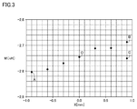
- FIG. 3 is a graph for explaining the relationship between the mutual inductance of the circuit device and the amount of deviation of the wiring portion according to the first embodiment.
- the horizontal axis is the deviation amount X (mm)
- the vertical axis is the mutual inductance M (nH) between the coil L1 and the coil L2.
- a circuit device in which the deviation amount X of the wiring 61 and the deviation amount Y of the wiring 71 are the same will be described.
- the point A shown in FIG. 3 is the mutual inductance M of the coil component 1 in the circuit device 10A.
- the mutual inductance M of the coil component 1 in the circuit device when the deviation amount X is 0 (zero) is shown at the point O.
- the mutual inductance M can be reduced by about 0.06 nH (about 2%) with respect to the point O.
- FIG. 4 is a plan view of another pattern of the circuit device according to the first embodiment.
- the wiring 61 is connected to the land electrode 60 by shifting the wiring 61 from the center of the side surface of the coil component 1 in the positive direction, and the wiring 71 is shifted in the positive direction from the center of the side surface of the coil component 1 to the land electrode 70.
- the connected circuit device 10B is shown.
- the wiring 61 is connected to the land electrode 60 by shifting the wiring 61 from the center of the side surface of the coil component 1 in the positive direction, and the wiring 71 is shifted in the negative direction from the center of the side surface of the coil component 1 to the land electrode 70.
- the connected circuit device 10C is shown. Among the circuit devices shown in FIG.
- the same configurations as those shown in FIG. 1 are designated by the same reference numerals, and detailed description thereof will not be repeated.
- the deviation amounts X, Y and the deviation directions of the wirings 61 and 71 shown in FIG. 4 are defined in the same manner as the deviation amounts X and Y and the deviation directions of the wirings 61 and 71 shown in FIG.
- the wiring 61 is shifted in the positive direction from the center of the side surface of the coil component 1 and connected to the land electrode 60, so that the current flowing through the land electrode 60 is indicated by a solid arrow. It flows along the side surface of the coil component 1 toward the wiring 61.
- the current flowing through the coil component 1 (for example, the current flowing through the second wiring pattern 20) flows substantially parallel to the current flowing through the land electrode 60 as shown by the broken line arrow in FIG. 4A. Therefore, the magnetic field generated by the current flowing through the land electrode 60 strengthens the magnetic field generated by the current flowing through the coil component 1.
- the current flowing through the land electrode 70 is the wiring 71 as shown by the solid arrow in FIG. 4 (a). It flows along the side surface of the coil component 1 toward.
- the current flowing through the coil component 1 (for example, the current flowing through the second wiring pattern 20) flows substantially parallel to the current flowing through the land electrode 70 as shown by the broken line arrow in FIG. 4A. Therefore, the magnetic field generated by the current flowing through the land electrode 70 strengthens the magnetic field generated by the current flowing through the coil component 1.
- Point B shown in FIG. 3 is the mutual inductance M of the coil component 1 in the circuit device 10B. As shown at the point B, by setting the deviation amount X to +0.9 mm, the mutual inductance M can be increased by about 0.06 nH (about 2%) with respect to the point O.
- the wiring 61 is shifted in the positive direction from the center of the side surface of the coil component 1 and connected to the land electrode 60, so that the current flowing through the land electrode 60 is indicated by a solid arrow. It flows along the side surface of the coil component 1 toward the wiring 61.
- the current flowing through the coil component 1 (for example, the current flowing through the second wiring pattern 20) flows substantially parallel to the current flowing through the land electrode 60 as shown by the broken line arrow in FIG. 4B. Therefore, the magnetic field generated by the current flowing through the land electrode 60 strengthens the magnetic field generated by the current flowing through the coil component 1.
- the current flowing through the land electrode 70 is the wiring 71 as shown by the solid arrow in FIG. 4 (b). It flows along the side surface of the coil component 1 toward.
- the current flowing through the coil component 1 (for example, the current flowing through the second wiring pattern 20) flows substantially opposite to the current flowing through the land electrode 70 as shown by the broken line arrow in FIG. 4 (b). Therefore, the magnetic field generated by the current flowing through the land electrode 70 weakens the magnetic field generated by the current flowing through the coil component 1.
- Point C shown in FIG. 3 is the mutual inductance M of the coil component 1 in the circuit device 10C.
- the deviation amount X of the wiring 61 is set to +0.9 mm
- the deviation amount X of the wiring 71 is set to -0.9 mm (in the graph of FIG. 3, the deviation amount X of the wiring 61 is used to set the point C only.
- the mutual inductance M becomes almost the same as the point O. That is, the circuit device 10C has a mutual inductance M equivalent to that of a circuit device having a deviation amount X of 0 (zero) as a whole by strengthening the magnetic field on the land electrode 60 side and weakening the magnetic field on the land electrode 70 side.
- FIG. 5 is a plan view of still another pattern of the circuit device according to the first embodiment.
- FIG. 5A shows a circuit device 10D in which the wiring 61 is connected to the land electrode 60 by shifting the wiring 61 from the center of the side surface of the coil component 1 in the negative direction, and the wiring 71 is connected to the land electrode 70 at the center of the side surface of the coil component 1. Is shown.
- FIG. 5A shows a circuit device 10D in which the wiring 61 is connected to the land electrode 60 by shifting the wiring 61 from the center of the side surface of the coil component 1 in the negative direction, and the wiring 71 is connected to the land electrode 70 at the center of the side surface of the coil component 1. Is shown.
- FIG. 5A shows a circuit device 10D in which the wiring 61 is connected to the land electrode 60 by shifting the wiring 61 from the center of the side surface of the coil component 1 in the negative direction, and the wiring 71 is connected to the land electrode 70 at the center of the side surface of the coil component 1. Is shown.
- 5B shows a circuit device 10E in which the wiring 61 is connected to the land electrode 60 by shifting the wiring 61 from the center of the side surface of the coil component 1 in the positive direction, and the wiring 71 is connected to the land electrode 70 at the center of the side surface of the coil component 1. Is shown.
- the same configurations as those shown in FIG. 1 are designated by the same reference numerals, and detailed description thereof will not be repeated.
- the deviation amounts X, Y and the deviation directions of the wirings 61 and 71 shown in FIG. 5 are defined in the same manner as the deviation amounts X and Y and the deviation directions of the wirings 61 and 71 shown in FIG.
- the wiring 61 is shifted in the negative direction from the center of the side surface of the coil component 1 and connected to the land electrode 60, so that the current flowing through the land electrode 60 is indicated by a solid arrow. It flows along the side surface of the coil component 1 toward the wiring 61.
- the current flowing through the coil component 1 (for example, the current flowing through the second wiring pattern 20) flows substantially opposite to the current flowing through the land electrode 60 as shown by the broken line arrow in FIG. 5A. Therefore, the magnetic field generated by the current flowing through the land electrode 60 weakens the magnetic field generated by the current flowing through the coil component 1.
- the current flowing through the land electrode 70 is directed to the side surface of the coil component 1 as shown by the solid arrow in FIG. 5 (a). It flows almost vertically.
- the current flowing through the coil component 1 (for example, the current flowing through the second wiring pattern 20) flows substantially perpendicular to the current flowing through the land electrode 70 as shown by the broken line arrow in FIG. 5A. Therefore, the magnetic field generated by the current flowing through the land electrode 70 does not affect the magnetic field generated by the current flowing through the coil component 1.
- the mutual inductance M of the coil component 1 in the circuit device 10D is larger than the mutual inductance M of the coil component 1 in the circuit device 10A, and is larger than the mutual inductance M of the coil component 1 in the circuit device having a deviation amount X of 0 (zero). Is small.
- the wiring 61 is shifted in the positive direction from the center of the side surface of the coil component 1 and connected to the land electrode 60, so that the current flowing through the land electrode 60 is indicated by a solid arrow. It flows along the side surface of the coil component 1 toward the wiring 61.
- the current flowing through the coil component 1 (for example, the current flowing through the second wiring pattern 20) flows substantially parallel to the current flowing through the land electrode 60 as shown by the broken line arrow in FIG. 5 (b). Therefore, the magnetic field generated by the current flowing through the land electrode 60 strengthens the magnetic field generated by the current flowing through the coil component 1.
- the current flowing through the land electrode 70 is directed to the side surface of the coil component 1 as shown by the solid arrow in FIG. 5 (b). It flows almost vertically.
- the current flowing through the coil component 1 (for example, the current flowing through the second wiring pattern 20) flows substantially perpendicular to the current flowing through the land electrode 70 as shown by the broken line arrow in FIG. 5 (b). Therefore, the magnetic field generated by the current flowing through the land electrode 70 does not affect the magnetic field generated by the current flowing through the coil component 1.
- the mutual inductance M of the coil component 1 in the circuit device 10E is smaller than the mutual inductance M of the coil component 1 in the circuit device 10B, and is larger than the mutual inductance M of the coil component 1 in the circuit device having a deviation amount X of 0 (zero). Is big.
- FIG. 6 is a circuit diagram of a filter circuit including a coil component according to the first embodiment.
- the filter circuit 100 is, for example, an EMI removal filter and is a third-order T-type LC filter circuit. Circuit devices 10A to 10E are used in the filter circuit 100. In the following first embodiment, a third-order T-type LC filter circuit will be used as the configuration of the filter circuit 100, but a fifth-order T-type LC filter circuit and a higher-order T-type LC filter circuit will be described. A multilayer substrate having the same configuration can be applied to the above. First, as shown in FIG. 6, the filter circuit 100 includes a capacitor C1, electrodes 4a, 4b, 4c, a coil L1 (first coil), and a coil L2 (second coil).
- the capacitor C1 has one end connected to the electrode 4c and the other end connected to the GND wiring.
- the capacitor C1 is not only a multilayer ceramic capacitor containing BaTiO3 (barium titanate) as a main component, but also a multilayer ceramic capacitor containing another material as a main component, which is not a multilayer ceramic capacitor, for example, an aluminum electrolytic capacitor or the like. It may be a type of capacitor.
- the capacitor C1 has an inductor L3 as a parasitic inductance (equivalent series inductance (ESL)), which is equivalent to a circuit configuration in which the inductor L3 is connected in series with the capacitor C1a.
- the capacitor C1 may be equivalent to a circuit configuration in which a parasitic resistance (equivalent series resistance (ESR)) is further connected in series with the inductor L3 and the capacitor C1a.
- the coil L1 and the coil L2 are connected to the electrode 4c.
- the coil L1 and the coil L2 are magnetically coupled to generate a negative inductance component (mutual inductance M).
- the parasitic inductance (inductor L3) of the capacitor C1 can be canceled, and the inductance component of the capacitor C1 can be apparently reduced.
- the filter circuit 100 composed of the capacitor C1, the coil L1 and the coil L2 has a negative inductance component due to the mutual inductance M between the coil L1 and the coil L2, and cancels the parasitic inductance of the capacitor C1 to suppress noise in the high frequency band. Can be improved.
- the circuit device 10A includes a substrate 2 on which a wiring pattern is formed and a coil component 1 mounted on the substrate 2.
- the coil component 1 includes a coil L1 (first coil) and a coil L2 (second coil) provided in the stack so that the coil surfaces face each other in the stacking direction, and each coil surface is parallel to the surface of the substrate 2.
- the wiring pattern includes a land electrode 70 (first electrode portion) connected to the electrode 4b (input terminal) of the coil component 1 and provided along the first side surface of the laminate 3 forming the electrode 4b, and the coil component.
- a land electrode 60 (second electrode portion) connected to the electrode 4a (output terminal) of 1 and provided along the second side surface of the laminated body 3 facing the first side surface is included.
- the wiring pattern is a wiring 71 (first wiring portion) that is electrically connected to the land electrode 70 at a position shifted by a deviation amount X (first distance) along the first side surface from the center of the first side surface. ), And the wiring 61 (second wiring portion) electrically connected to the land electrode 60 at a position shifted by the amount of deviation Y (second distance) along the second side surface from the center of the second side surface. including.
- a current can flow along the side surface of the laminate 3 by the land electrode 60 and the wiring 61, and the land electrode 70 and the wiring 71, so that the current flows through the coil component 1.
- the magnetic field generated by the current can be weakened or strengthened by the magnetic field generated by the current flowing through the land electrodes 60 and 70, and the mutual inductance M of the coil component 1 can be adjusted.
- the deviation amount X and the deviation amount Y may be the same distance as in the circuit devices 10A to 10C.
- the wiring 61 and the wiring 71 may be displaced along the side surface of the laminated body 3 in the same direction as in the circuit devices 10A and 10B.
- the wiring 61 and the wiring 71 may be displaced along the side surface of the laminated body 3 in different directions as in the circuit device 10C.
- the deviation amount X or the deviation amount Y may include zero distance as in the circuit devices 10D and 10E.
- the first side surface and the second side surface of the coil component 1 are preferably surfaces parallel to the longitudinal direction of the coil component 1.
- the land electrodes 60 and 70 can be provided along the longitudinal direction of the coil component 1.
- the current flowing through the coil component 1 is compared with the case where the land electrodes 60 and 70 are provided along the lateral direction of the coil component 1.
- the current paths of the land electrodes 60 and 70 that can affect the current can be lengthened.
- the coil component 1 is preferably a transformer coil in which the coil L1 and the coil L2 are magnetically coupled. It is preferable that the coil component 1 has a portion in which the first wiring pattern 10 to the third wiring pattern 30 (conductor) constituting the coil L1 and the coil L2 are along the first side surface and the second side surface, respectively.
- the filter circuit 100 includes circuit devices 10A to 10E and a capacitor C1 connected to an electrode 4c between the coil L1 and the coil L2 of the coil component 1. As a result, the filter circuit 100 can improve the noise suppression effect in the high frequency band by canceling the parasitic inductance of the capacitor C1.
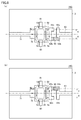
- FIG. 7 is a plan view of the circuit device according to the second embodiment.
- the alternate long and short dash line shown in FIG. 7 represents the side surface of the coil component 1 and the center of the wiring, and the lower side in the figure is the minus (negative) direction and the upper side in the figure is the plus (positive) direction.
- the coil component 1 is mounted on the surface of the substrate 2.
- Land electrodes 62, 72, 80, 81 for surface mounting the coil component 1 are formed on the surface of the substrate 2.
- the land electrode 62 is connected to an electrode 4a which is an output terminal for outputting a current from the coil component 1
- the land electrode 72 is connected to an electrode 4b which is an input terminal for inputting a current to the coil component 1.
- the direction of the current flowing through the coil component 1 can be changed, and the current may be input using the electrode 4a as an input terminal and the current may be output using the electrode 4b as an output terminal.
- the land electrode 62 has a connection portion 62a (first A connection portion) at a position deviated by a positive amount X (first distance) from the center of the side surface (first side surface forming the electrode 4a) of the coil component 1.
- a connecting portion 62b (first B connecting portion) is provided at a position shifted by the amount of deviation X in the negative direction.
- the wiring 63 is provided with an end portion 63a (first A end portion) extended to a position facing the connecting portion 62a and an end portion 63b (first B end portion) extended to a position facing the connecting portion 62b. is there.
- connection portion 62a and the end portion 63a are connected by the connecting element 90 (for example, a 0 ohm chip) or the connecting portion 62b and the end portion 63b are connected by the connecting element 90. can do.
- the land electrode 72 is connected to the connection portion 72a (second A connection portion) at a position shifted by a positive amount Y (second distance) from the center of the side surface of the coil component 1 and at a position shifted by a deviation amount Y in the negative direction.
- a portion 72b (second B connection portion) is provided.
- the wiring 73 is provided with an end portion 73a (second A end portion) extended to a position facing the connecting portion 72a and an end portion 73b (second B end portion) extended to a position facing the connecting portion 72b. is there.
- connecting portion 72a and the end portion 73a are connected by the connecting element 91 (for example, a 0 ohm chip) or the connecting portion 72b and the end portion 73b are connected by the connecting element 91. can do.
- the connecting element 90 connects the connecting portion 62b and the end portion 63b
- the connecting element 91 connects the connecting portion 72a and the end portion 73a. Therefore, in the circuit device 15A, the wiring 63 and the land electrode 62 are connected at a position deviated by an amount X in the negative direction from the center of the side surface of the coil component 1, and the current flowing through the land electrode 62 is shown in FIG. 7 ( As shown by the solid arrow in a), the current flows along the side surface of the coil component 1 toward the connection portion 62b. On the other hand, the current flowing through the coil component 1 flows substantially opposite to the current flowing through the land electrode 62 as shown by the broken line arrow in FIG. 7A. The magnetic field generated by the current flowing through the land electrode 62 weakens the magnetic field generated by the current flowing through the coil component 1.
- the wiring 73 and the land electrode 72 are connected at a position deviated by an amount Y in the positive direction from the center of the side surface of the coil component 1, and the current flowing through the land electrode 72 is shown in FIG. 7 ( As shown by the solid arrow in a), the current flows toward the connection portion 72b along the side surface of the coil component 1.
- the current flowing through the coil component 1 flows substantially parallel to the current flowing through the land electrode 72 as shown by the broken line arrow in FIG. 7A.
- the magnetic field generated by the current flowing through the land electrode 72 strengthens the magnetic field generated by the current flowing through the coil component 1.
- the connecting element 90 connects the connecting portion 62a and the end portion 63a
- the connecting element 91 connects the connecting portion 72a and the end portion 73a. Therefore, in the circuit device 15B, the wiring 63 and the land electrode 62 are connected at a position deviated by an amount X in the positive direction from the center of the side surface of the coil component 1, and the current flowing through the land electrode 62 is shown in FIG. 7 ( As shown by the solid arrow in b), the current flows toward the connection portion 62a along the side surface of the coil component 1. On the other hand, the current flowing through the coil component 1 flows substantially parallel to the current flowing through the land electrode 62 as shown by the broken line arrow in FIG. 7B. The magnetic field generated by the current flowing through the land electrode 62 strengthens the magnetic field generated by the current flowing through the coil component 1.
- the wiring 73 and the land electrode 72 are connected at a position deviated by an amount Y in the positive direction from the center of the side surface of the coil component 1, and the current flowing through the land electrode 72 is shown in FIG. 7 ( As shown by the solid arrow in b), the current flows toward the connection portion 72a along the side surface of the coil component 1.
- the current flowing through the coil component 1 flows substantially parallel to the current flowing through the land electrode 72 as shown by the broken line arrow in FIG. 7B.
- the magnetic field generated by the current flowing through the land electrode 72 strengthens the magnetic field generated by the current flowing through the coil component 1.
- FIG. 8 is a plan view of still another pattern of the circuit device according to the second embodiment.
- connecting portions 62a and 62b are provided on the land electrode 62 and connected to the wiring 63, and the wiring 71 is connected to the land electrode 70 at the center of the side surface of the coil component 1.
- the connecting portion 62b and the end portion 63b are connected by the connecting element 90.
- the connecting element 90 connects the connecting portion 62a and the end portion 63a.
- the land electrode 62 (first electrode portion) is in the positive direction (first) from the center of the first side surface along the first side surface.
- Amount of deviation X (first distance) in the direction) The amount of deviation between the connection portion 62a (first A connection portion) and the minus direction (second direction) along the first side surface from the center of the first side surface. It has a connecting portion 62b (first B connecting portion) at a position shifted by X.
- the land electrode 72 (second electrode portion) has a connection portion 72a (second A connection portion) displaced from the center of the second side surface by a positive amount Y (second distance) along the second side surface.
- a connection portion 72b (second B connection portion) is provided at a position shifted by a negative amount Y from the center of the second side surface along the second side surface.
- the wiring 63 (first wiring portion) has an end portion 63a (first A end portion) extended to a position facing the connecting portion 62a and an end portion 63b (first B) extended to a position facing the connecting portion 62b. End) and.
- the wiring 73 (second wiring portion) has an end portion 73a (second A end portion) extended to a position facing the connecting portion 72a and an end portion 73b (second B) extended to a position facing the connecting portion 72b. End) and.
- the circuit devices 15A and 15B include a connecting element 90 (first connecting element) that electrically connects between the connecting portion 62a and the end portion 63a, or between the connecting portion 62b and the end portion 63b, and the connecting portion 72a.
- a connection element 91 (second connection element) for electrically connecting between the end portion 73a or between the connection portion 72b and the end portion 73b is provided.
- a current can flow along the side surface of the laminate 3 by the land electrode 62 and the wiring 63, and the land electrode 72 and the wiring 73, so that the coil component 1
- the magnetic field generated by the current flowing through the land electrodes 62 and 72 can be weakened or strengthened by the magnetic field generated by the current flowing through the land electrodes 62 and 72, and the mutual inductance M of the coil component 1 can be adjusted.
- the filter circuit includes circuit devices 15A to 15D and a capacitor C1 connected to an electrode 4c between the coil L1 and the coil L2 of the coil component 1.
- the filter circuit can improve the noise suppression effect in the high frequency band by canceling the parasitic inductance of the capacitor C1.
- connection portion 62a and the end portion 63a or the connection portion 62b and the end portion 63b are electrically connected by the connection element 90, or the connection portion 72a and the end portion 72a and the end portion are electrically connected.
- connection element 91 can be electrically connected between the portion 73a or between the connection portion 72b and the end portion 73b has been described.
- the configuration of a circuit device capable of selecting the presence or absence of the coil component 1 at the time of mounting the component will be described.
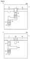
- FIG. 9 is a plan view of the circuit device according to the third embodiment.
- FIG. 9A is a plan view of the circuit device 18A on which the coil component 1 is mounted
- FIG. 9B is a plan view of the circuit device 18B on which the coil component 1 is not mounted.
- a land electrode for mounting the coil component 1, capacitors C1, C2, and the like, and a wiring pattern of wiring are commonly formed on the surface of the substrate 2.
- the wiring pattern includes wirings 65 and 75 for connecting to the input / output terminals of the coil component 1, and land electrodes 85 for connecting the coil component 1 and the capacitor C1.
- a wiring 86 connecting the capacitor C1 and the capacitor C2 and a land electrode 87 connecting the capacitor C2 are included.
- the coil component 1 is mounted at a position where the wirings 65 and 75 and the land electrode 85 are connected.
- the capacitor C1 is mounted at a position where the land electrode 85 and the wiring 86 are connected.
- a connecting element 300 (for example, a 0 ohm chip or the like) is mounted to connect the wiring 65 and the wiring 75.
- the capacitor C1 is mounted between the wiring 75 and the wiring 86 without mounting the capacitor C1 at the position where the land electrode 85 and the wiring 86 are connected.
- the circuit devices 18A and 18B have land electrodes 85, wiring 86, and the like so that the position where the capacitor C1 is provided can be changed depending on whether or not the coil component 1 is mounted. The position where the capacitor C2 is mounted is not changed.
- FIG. 10 is a plan view of another pattern of the circuit device according to the third embodiment.
- FIG. 10A is a plan view of the circuit device 18C on which the coil component 1 is mounted
- FIG. 10B is a plan view of the circuit device 18D on which the coil component 1 is not mounted.
- the wiring pattern of the land electrode and the wiring on which the coil component 1, the capacitors C1 and C2 and the like are mounted is commonly formed on the surface of the substrate 2.
- the wiring patterns of the circuit device 18C and the circuit device 18D are different in the shape of the wiring 86a as compared with the wiring patterns of the circuit device 18A and the circuit device 18B.
- the wiring 86 has a shape so that the capacitor C1 and the capacitor C2 can be mounted in a straight line when the coil component 1 is not mounted.
- the wiring 86a has a shape so that the capacitor C1 and the capacitor C2 can be mounted on a straight line when the coil component 1 is mounted.
- FIG. 11 is a plan view of a circuit device and a comparative example according to the third embodiment.
- FIG. 11A is a plan view of the circuit device 18E on which the coil component 1 is mounted
- FIG. 11B is a plan view of the circuit device 18F on which the coil component 1 is not mounted.
- a land electrode for mounting the coil component 1, capacitors C1, C2, and the like, and a wiring pattern of wiring are commonly formed on the surface of the substrate 2.
- the wiring pattern includes wirings 65 and 75 for connecting to the input / output terminals of the coil component 1, and land electrodes 85 for connecting the coil component 1 and the capacitor C1.
- a wiring 86b connecting the capacitor C1 and the capacitor C2 and a land electrode 87b connecting the capacitor C2 are included.
- the wiring pattern includes a wiring 86c that connects the capacitor C1 and the capacitor C2 when the coil component 1 is not mounted, and a land electrode 87c that connects the capacitor C2. ..
- the circuit devices 18A to 18D shown in FIGS. 9 and 10 have a wiring pattern that does not change the position where the capacitor C2 is provided depending on whether or not the coil component 1 is mounted. It is formed so that the mounting area of the component on the substrate 2 can be reduced. In the circuit devices 18A to 18D shown in FIGS. 9 and 10, it is only necessary to form a wiring pattern on the surface of the substrate 2 in which only the position where the capacitor C1 is mounted can be changed.
Landscapes
- Engineering & Computer Science (AREA)
- Power Engineering (AREA)
- Microelectronics & Electronic Packaging (AREA)
- Multimedia (AREA)
- Coils Or Transformers For Communication (AREA)
- Filters And Equalizers (AREA)
Priority Applications (3)
| Application Number | Priority Date | Filing Date | Title |
|---|---|---|---|
| JP2021563795A JP7553470B2 (ja) | 2019-12-13 | 2020-11-09 | 回路装置、およびフィルタ回路 |
| CN202090000896.2U CN217216514U (zh) | 2019-12-13 | 2020-11-09 | 电路装置以及滤波器电路 |
| US17/715,098 US12040768B2 (en) | 2019-12-13 | 2022-04-07 | Circuit device and filter circuit |
Applications Claiming Priority (2)
| Application Number | Priority Date | Filing Date | Title |
|---|---|---|---|
| JP2019-225302 | 2019-12-13 | ||
| JP2019225302 | 2019-12-13 |
Related Child Applications (1)
| Application Number | Title | Priority Date | Filing Date |
|---|---|---|---|
| US17/715,098 Continuation US12040768B2 (en) | 2019-12-13 | 2022-04-07 | Circuit device and filter circuit |
Publications (1)
| Publication Number | Publication Date |
|---|---|
| WO2021117393A1 true WO2021117393A1 (ja) | 2021-06-17 |
Family
ID=76329755
Family Applications (1)
| Application Number | Title | Priority Date | Filing Date |
|---|---|---|---|
| PCT/JP2020/041687 Ceased WO2021117393A1 (ja) | 2019-12-13 | 2020-11-09 | 回路装置、およびフィルタ回路 |
Country Status (4)
| Country | Link |
|---|---|
| US (1) | US12040768B2 (https=) |
| JP (1) | JP7553470B2 (https=) |
| CN (1) | CN217216514U (https=) |
| WO (1) | WO2021117393A1 (https=) |
Cited By (1)
| Publication number | Priority date | Publication date | Assignee | Title |
|---|---|---|---|---|
| WO2024166971A1 (ja) * | 2023-02-09 | 2024-08-15 | 株式会社村田製作所 | 回路装置、および回路基板 |
Families Citing this family (1)
| Publication number | Priority date | Publication date | Assignee | Title |
|---|---|---|---|---|
| KR102335426B1 (ko) * | 2020-01-07 | 2021-12-06 | 삼성전기주식회사 | 코일 부품 |
Citations (5)
| Publication number | Priority date | Publication date | Assignee | Title |
|---|---|---|---|---|
| JP2008167157A (ja) * | 2006-12-28 | 2008-07-17 | Toko Inc | ハイパスフィルタ |
| WO2009011400A1 (ja) * | 2007-07-17 | 2009-01-22 | Murata Manufacturing Co., Ltd. | 無線icデバイス及び電子機器 |
| JP2010135602A (ja) * | 2008-12-05 | 2010-06-17 | Murata Mfg Co Ltd | ノイズ対策部品及びその接続構造 |
| JP2017201667A (ja) * | 2016-05-06 | 2017-11-09 | 株式会社村田製作所 | 高周波ノイズ対策回路 |
| WO2018066578A1 (ja) * | 2016-10-07 | 2018-04-12 | 株式会社村田製作所 | フィルタ |
Family Cites Families (1)
| Publication number | Priority date | Publication date | Assignee | Title |
|---|---|---|---|---|
| JP2001160728A (ja) | 1999-09-21 | 2001-06-12 | Murata Mfg Co Ltd | Lcフィルタ |
-
2020
- 2020-11-09 JP JP2021563795A patent/JP7553470B2/ja active Active
- 2020-11-09 WO PCT/JP2020/041687 patent/WO2021117393A1/ja not_active Ceased
- 2020-11-09 CN CN202090000896.2U patent/CN217216514U/zh active Active
-
2022
- 2022-04-07 US US17/715,098 patent/US12040768B2/en active Active
Patent Citations (5)
| Publication number | Priority date | Publication date | Assignee | Title |
|---|---|---|---|---|
| JP2008167157A (ja) * | 2006-12-28 | 2008-07-17 | Toko Inc | ハイパスフィルタ |
| WO2009011400A1 (ja) * | 2007-07-17 | 2009-01-22 | Murata Manufacturing Co., Ltd. | 無線icデバイス及び電子機器 |
| JP2010135602A (ja) * | 2008-12-05 | 2010-06-17 | Murata Mfg Co Ltd | ノイズ対策部品及びその接続構造 |
| JP2017201667A (ja) * | 2016-05-06 | 2017-11-09 | 株式会社村田製作所 | 高周波ノイズ対策回路 |
| WO2018066578A1 (ja) * | 2016-10-07 | 2018-04-12 | 株式会社村田製作所 | フィルタ |
Cited By (2)
| Publication number | Priority date | Publication date | Assignee | Title |
|---|---|---|---|---|
| WO2024166971A1 (ja) * | 2023-02-09 | 2024-08-15 | 株式会社村田製作所 | 回路装置、および回路基板 |
| JPWO2024166971A1 (https=) * | 2023-02-09 | 2024-08-15 |
Also Published As
| Publication number | Publication date |
|---|---|
| US20220231653A1 (en) | 2022-07-21 |
| CN217216514U (zh) | 2022-08-16 |
| JP7553470B2 (ja) | 2024-09-18 |
| US12040768B2 (en) | 2024-07-16 |
| JPWO2021117393A1 (https=) | 2021-06-17 |
Similar Documents
| Publication | Publication Date | Title |
|---|---|---|
| CN216162684U (zh) | 线圈部件及包含该线圈部件的滤波器电路 | |
| US12355416B2 (en) | Coil component, filter circuit including the coil component, and electronic device | |
| JP7318815B2 (ja) | フィルタ回路および、これを含む電源装置 | |
| JPWO2020121592A1 (ja) | コイル部品および、これを含むフィルタ回路 | |
| JP6981584B2 (ja) | 多層基板、回路装置、およびフィルタ回路基板 | |
| JP7553470B2 (ja) | 回路装置、およびフィルタ回路 | |
| US11264162B2 (en) | Coil component and filter circuit including the coil component | |
| JP6500989B2 (ja) | 回路基板、これを用いたフィルタ回路およびキャパシタンス素子 | |
| JPWO2020246118A1 (ja) | 回路素子 | |
| US10284164B2 (en) | Circuit substrate, filter circuit, and capacitance element | |
| US20240297631A1 (en) | Circuit device | |
| WO2022137678A1 (ja) | コイル部品および、これを含むフィルタ回路 |
Legal Events
| Date | Code | Title | Description |
|---|---|---|---|
| 121 | Ep: the epo has been informed by wipo that ep was designated in this application |
Ref document number: 20898587 Country of ref document: EP Kind code of ref document: A1 |
|
| ENP | Entry into the national phase |
Ref document number: 2021563795 Country of ref document: JP Kind code of ref document: A |
|
| NENP | Non-entry into the national phase |
Ref country code: DE |
|
| 122 | Ep: pct application non-entry in european phase |
Ref document number: 20898587 Country of ref document: EP Kind code of ref document: A1 |