WO2021100526A1 - 発光素子駆動回路および発光装置 - Google Patents
発光素子駆動回路および発光装置 Download PDFInfo
- Publication number
- WO2021100526A1 WO2021100526A1 PCT/JP2020/041781 JP2020041781W WO2021100526A1 WO 2021100526 A1 WO2021100526 A1 WO 2021100526A1 JP 2020041781 W JP2020041781 W JP 2020041781W WO 2021100526 A1 WO2021100526 A1 WO 2021100526A1
- Authority
- WO
- WIPO (PCT)
- Prior art keywords
- light emitting
- emitting element
- circuit
- voltage
- current
- Prior art date
- Legal status (The legal status is an assumption and is not a legal conclusion. Google has not performed a legal analysis and makes no representation as to the accuracy of the status listed.)
- Ceased
Links
Images





Classifications
-
- H—ELECTRICITY
- H05—ELECTRIC TECHNIQUES NOT OTHERWISE PROVIDED FOR
- H05B—ELECTRIC HEATING; ELECTRIC LIGHT SOURCES NOT OTHERWISE PROVIDED FOR; CIRCUIT ARRANGEMENTS FOR ELECTRIC LIGHT SOURCES, IN GENERAL
- H05B45/00—Circuit arrangements for operating light-emitting diodes [LED]
- H05B45/30—Driver circuits
- H05B45/37—Converter circuits
- H05B45/3725—Switched mode power supply [SMPS]
- H05B45/38—Switched mode power supply [SMPS] using boost topology
-
- H—ELECTRICITY
- H01—ELECTRIC ELEMENTS
- H01S—DEVICES USING THE PROCESS OF LIGHT AMPLIFICATION BY STIMULATED EMISSION OF RADIATION [LASER] TO AMPLIFY OR GENERATE LIGHT; DEVICES USING STIMULATED EMISSION OF ELECTROMAGNETIC RADIATION IN WAVE RANGES OTHER THAN OPTICAL
- H01S5/00—Semiconductor lasers
- H01S5/06—Arrangements for controlling the laser output parameters, e.g. by operating on the active medium
- H01S5/062—Arrangements for controlling the laser output parameters, e.g. by operating on the active medium by varying the potential of the electrodes
-
- H—ELECTRICITY
- H05—ELECTRIC TECHNIQUES NOT OTHERWISE PROVIDED FOR
- H05B—ELECTRIC HEATING; ELECTRIC LIGHT SOURCES NOT OTHERWISE PROVIDED FOR; CIRCUIT ARRANGEMENTS FOR ELECTRIC LIGHT SOURCES, IN GENERAL
- H05B47/00—Circuit arrangements for operating light sources in general, i.e. where the type of light source is not relevant
- H05B47/10—Controlling the light source
-
- H—ELECTRICITY
- H10—SEMICONDUCTOR DEVICES; ELECTRIC SOLID-STATE DEVICES NOT OTHERWISE PROVIDED FOR
- H10H—INORGANIC LIGHT-EMITTING SEMICONDUCTOR DEVICES HAVING POTENTIAL BARRIERS
- H10H20/00—Individual inorganic light-emitting semiconductor devices having potential barriers, e.g. light-emitting diodes [LED]
- H10H20/80—Constructional details
-
- H—ELECTRICITY
- H05—ELECTRIC TECHNIQUES NOT OTHERWISE PROVIDED FOR
- H05B—ELECTRIC HEATING; ELECTRIC LIGHT SOURCES NOT OTHERWISE PROVIDED FOR; CIRCUIT ARRANGEMENTS FOR ELECTRIC LIGHT SOURCES, IN GENERAL
- H05B45/00—Circuit arrangements for operating light-emitting diodes [LED]
- H05B45/30—Driver circuits
- H05B45/345—Current stabilisation; Maintaining constant current
Definitions
- the present disclosure relates to a light emitting element drive circuit and a light emitting device.
- a light emitting device including a light emitting element such as a laser diode (LD) or an LED (Light Emitting Diode) is provided with a light emitting element drive circuit that supplies a drive current to the light emitting element (for example, Patent Document 1). reference).
- a light emitting element such as a laser diode (LD) or an LED (Light Emitting Diode)
- a light emitting element drive circuit that supplies a drive current to the light emitting element
- the present disclosure proposes a light emitting element drive circuit and a light emitting device that can achieve both a reduction in the rise time of the light emitting element and a reduction in power consumption.
- a light emitting element drive circuit includes a constant current circuit, a switch, and a booster circuit.
- the constant current circuit supplies a constant current to the light emitting element from the power supply voltage.
- the switch interrupts the current flowing through the light emitting element based on an external signal.
- the booster circuit boosts the voltage between the power supply voltage and the light emitting element in synchronization with the timing at which the light emitting element is turned on.
- a light emitting device including a light emitting element such as a laser diode (LD) or an LED (Light Emitting Diode) is provided with a light emitting element drive circuit that supplies a drive current to the light emitting element.
- a light emitting element such as a laser diode (LD) or an LED (Light Emitting Diode)
- LD laser diode
- LED Light Emitting Diode
- this light emitting element drive circuit a technique is known in which a weak current is passed before the light emitting element is made to emit light to shorten the rise time when the light emitting element emits light.
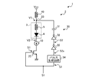
- FIG. 1 is a circuit diagram showing a configuration example of a light emitting device 1 and a light emitting element drive circuit 2 according to the embodiment of the present disclosure.
- the light emitting device 1 includes a light emitting element drive circuit 2 and a light emitting element 3.
- the light emitting element 3 emits light by supplying a drive current from the light emitting element drive circuit 2 to the light emitting element 3.
- the light emitting element 3 is, for example, a laser diode or an LED.
- the light emitting element 3 has a diode 4 that emits light when a drive current is supplied from the light emitting element drive circuit 2, and a parasitic inductor 5. Then, inside the light emitting element 3, the diode 4 and the parasitic inductor 5 are connected in series.
- the light emitting element drive circuit 2 includes a constant current circuit 10, a switch 20, a booster circuit 30, and an inductor element 40.
- the constant current circuit 10 supplies a predetermined constant current to the light emitting element 3 from the power supply voltage Vcc.
- the power supply voltage Vcc is a predetermined voltage (for example, 3.3 (V), 5 (V), etc.) capable of emitting light from the light emitting element 3.
- the switch 20 interrupts (disconnects or connects) the current flowing through the light emitting element 3 based on an external signal.
- the booster circuit 30 boosts the voltage between the power supply voltage Vcc and the light emitting element 3 in synchronization with the timing at which the light emitting element 3 is turned on.
- the inductor element 40 is provided between the power supply voltage Vcc and the light emitting element 3.
- the anode of the diode 4 in the light emitting element 3 is connected to the power supply voltage Vcc via the parasitic inductor 5 and the inductor element 40 connected in series.
- the cathode of the diode 4 is grounded via an N-type transistor 11 and a switch 20 connected in series.
- the N-type transistor 11 is a part of the constant current circuit 10, and the switch 20 is composed of an N-type transistor.
- the constant current circuit 10 includes an N-type transistor 11, an N-type transistor 12, a constant current source 13, an N-type transistor 14, and a capacitor 15.
- the N-type transistor 11 and the N-type transistor 12 are high withstand voltage transistors (for example, LDMOS) having substantially the same element characteristics, and form a current mirror.
- the gate of the N-type transistor 11 is connected to the gate of the N-type transistor 12, and the gate of the N-type transistor 12 is connected to the drain of the N-type transistor 12.
- the drain of the N-type transistor 12 is connected to the voltage VL for logic operation via the constant current source 13, and the source of the N-type transistor 12 is grounded via the N-type transistor 14.
- the voltage VL for logic operation is, for example, 1.8 (V).
- a voltage VL for logic operation is connected to the gate of the N-type transistor 14, and the gate of the N-type transistor 11 and the gate of the N-type transistor 12 are grounded via the capacitor 15.
- the constant current circuit 10 can pass a constant current through the N-type transistor 11 based on the constant current flowing from the constant current source 13 through the N-type transistor 12. As a result, the constant current circuit 10 can supply a constant current to the light emitting element 3 connected in series with the N-type transistor 11.
- the N-type transistor 11 and the N-type transistor 12 have substantially the same element characteristics, and the N-type transistor 14 has substantially the same element characteristics as the switch 20.
- the constant current circuit 10 can supply the light emitting element 3 with a stable constant current in which the mirror ratio of the current mirror is close to the element size.
- the drain of the switch 20 composed of the N-type transistor is connected to the light emitting element 3 via the N-type transistor 11 of the constant current circuit 10, and the source of the switch 20 is grounded. Further, a signal S1 from a control unit (not shown) is input to the gate of the switch 20.
- the signal S1 is an example of an external signal.
- the switch 20 When the signal S1 is at a high level, the switch 20 is in a conductive state, so that a predetermined constant current is supplied to the light emitting element 3 from the power supply voltage Vcc, and the light emitting element 3 is in a lighting state. On the other hand, when the signal S1 is at a low level, the switch 20 is in the disconnected state, so that a constant current is not supplied to the light emitting element 3 from the power supply voltage Vcc, and the light emitting element 3 is turned off.
- the booster circuit 30 has a capacitor 31 and an inverter 32. Further, the inverter 32 has a P-type transistor 32a and an N-type transistor 32b.
- the source of the P-type transistor 32a is connected to the voltage VL for logic operation, and the drain of the P-type transistor 32a is connected to the drain of the N-type transistor 32b via the node 32c.
- the node 32c corresponds to the output terminal of the inverter 32. Further, the source of the N-type transistor 32b is grounded.
- the capacitor 31 is provided between the node 32c, which is the output terminal of the inverter 32, and the node 33 provided between the power supply voltage Vcc and the light emitting element 3 (specifically, between the inductor element 40 and the light emitting element 3). Be done.
- FIG. 2 is a circuit diagram showing a configuration example of the light emitting device 1 and the light emitting element drive circuit 2 of Reference Example 1. As shown in FIG. 2, the light emitting device 1 of Reference Example 1 has the same configuration as that of the embodiment except that the booster circuit 30 is not provided.
- FIG. 3 is a timing chart showing an operation example of the light emitting element drive circuit 2 of Reference Example 1, showing a voltage V1, a signal S1, a voltage V2, and a current I1.
- the voltage V1 is the voltage on the input side of the light emitting element 3 (that is, the anode side of the diode 4), and the signal S1 is an external signal input to the gate of the switch 20.
- the voltage V2 is the voltage on the output side of the light emitting element 3 (that is, the cathode side of the diode 4)
- the current I1 is the output current of the light emitting element 3 (that is, the current output from the cathode of the diode 4). is there.
- the switch 20 As shown in FIG. 3, since the signal S1 is at a low level in the initial state, the switch 20 (see FIG. 2) is in the disconnected state. Therefore, in the initial state, the output current (current I1) of the light emitting element 3 is zero, and the light emitting element 3 is in the extinguished state.
- the voltage V1 on the input side and the voltage V2 on the output side of the light emitting element 3 are both substantially equal to the power supply voltage Vcc.
- this voltage V2 can be regarded as the output voltage of the constant current circuit 10 which is the current mirror circuit, but when the output voltage (voltage V2) of the current mirror circuit drops significantly in this way, the constant current circuit 10 The mirror ratio cannot be maintained.
- the current I1 finally reaches a predetermined constant current Ia at the time T2.
- FIG. 4 is a circuit diagram showing a configuration example of the light emitting device 1 and the light emitting element drive circuit 2 of Reference Example 2.
- the light emitting device 1 of Reference Example 2 has the same configuration as that of the embodiment except that the booster circuit 30 is not provided and the power supply voltage is Vcc + VL instead of Vcc.
- FIG. 5 is a timing chart showing an operation example of the light emitting element drive circuit 2 of Reference Example 2, and shows a voltage V1, a signal S1, a voltage V2, and a current I1 as in Reference Example 1.
- the switch 20 As shown in FIG. 5, since the signal S1 is at a low level in the initial state, the switch 20 (see FIG. 4) is in the disconnected state. Therefore, in the initial state, the output current (current I1) of the light emitting element 3 is zero, and the light emitting element 3 is in the extinguished state.
- the voltage V1 on the input side and the voltage V2 on the output side of the light emitting element 3 are both substantially equal to the power supply voltage Vcc + VL.
- the voltage V2 on the output side of the light emitting element 3 drops significantly to the voltage Va1.
- the value of the voltage Va1 is larger than the voltage Va of the modified example 1, and the mirror ratio of the constant current circuit 10 can be maintained. Is maintained at.
- the current required for the light emitting element 3 can be passed from the constant current circuit 10 faster, so that the current I1 is increased. Therefore, in the modified example 2, the current I1 reaches a predetermined constant current Ia at the time T2a before the time T2 in the modified example 1.
- the mirror ratio of the constant current circuit 10 can be maintained even when the light emitting element 3 rises by boosting the power supply voltage itself, so that the rising time of the light emitting element 3 (FIG. In 5, T2a-T1) can be shortened.
- the voltage Vb1 is larger than the voltage Vb in the first modification.
- the value of the voltage V2 becomes the voltage Vb1 larger than that of the modified example 1 during the period from the time T2a to the time T3 when the current I1 reaches the predetermined constant current Ia.
- the loss in the light emitting device 1 becomes large, so that the power consumption of the light emitting device 1 increases.
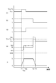
- FIG. 6 is a timing chart showing an operation example of the light emitting element drive circuit 2 according to the embodiment of the present disclosure, and shows a signal S2 in addition to the voltage V1, the signal S1, the voltage V2, and the current I1.
- the signal S2 is an external signal input to the input terminal of the inverter 32 in the booster circuit 30.
- the change in voltage V2 in Reference Example 2 is shown by a chain double-dashed line.
- the voltage V1 on the input side and the voltage V2 on the output side of the light emitting element 3 are both substantially equal to the power supply voltage Vcc.
- the P-type transistor 32a is in a disconnected state, and the N-type transistor 32b is in a conductive state.
- the power supply voltage Vcc and the ground voltage are applied to both terminals of the capacitor 31, respectively, and the capacitor 31 is charged so that the potential difference between both terminals becomes substantially equal to the power supply voltage Vcc.
- the signal S2 switches from the high level to the low level in synchronization with the signal S1.
- the P-type transistor 32a is in a conductive state and the N-type transistor 32b is in a disconnected state, so that the voltage at the output terminal (node 32c) of the inverter 32 changes from zero to the voltage VL.
- the voltage VL of the output terminal (node 32c) of the inverter 32 is added to the potential difference (voltage Vcc) of both terminals of the capacitor 31, and the voltage of the node 33 (that is, the voltage V1 on the input side of the light emitting element 3). Is boosted to Vcc + VL.
- the voltage of the node 33 is boosted by the booster circuit 30 in synchronization with the timing (time T1) when the light emitting element 3 is turned on.
- the voltage V2 on the output side of the light emitting element 3 drops significantly to the voltage Va1.
- the value of the voltage V2 can maintain the mirror ratio of the constant current circuit 10 as in the modification 2. The value (voltage Va1) is maintained.
- the current required for the light emitting element 3 can be passed from the constant current circuit 10 faster, the increase of the current I1 is promoted, and the current I1 becomes a predetermined value at the same time T2a as in the second modification.
- the constant current Ia is reached.
- the booster circuit 30 boosts the input side terminal of the light emitting element 3, so that the current of the mirror ratio of the constant current circuit 10 is increased faster even when the light emitting element 3 rises. Since it can be flowed, the rise time (T2a-T1) of the light emitting element 3 can be shortened.
- the signal S2 switches from the low level to the high level at the time T2b after the time T2a.
- the voltage at the output terminal (node 32c) of the inverter 32 changes from the voltage VL to zero, so that the node 33 is not boosted by the capacitor 31.
- the voltage V1 on the input side of the light emitting element 3 returns to a value substantially equal to the power supply voltage Vcc at time T2b.
- the voltage V2 on the output side of the light emitting element 3 also drops from the voltage Vb1 to the same voltage Vb as in the first modification at time T2b.
- the value of the voltage V2 can be reduced to a voltage Vb smaller than that of the modification 2 from the time T2b to the time T3.
- the loss in the light emitting device 1 can be reduced, so that the power consumption of the light emitting device 1 can be reduced.
- the rise time of the light emitting element 3 is shortened by boosting the input side terminal of the light emitting element 3 by the booster circuit 30 in synchronization with the timing when the light emitting element 3 is turned on. It is possible to achieve both reduction of power consumption.
- the terminal on the input side of the light emitting element 3 can be stably boosted.
- the booster circuit 30 does not necessarily have to be configured by using the capacitor 31 and the inverter 32, and the terminal on the input side of the light emitting element 3 may be boosted by using another known booster circuit.
- the power supply voltage Vcc which is higher than the logic voltage VL, is generated by the light emitting element 3. Can be connected to.
- the drive current of the light emitting element 3 can be increased. Further, in the embodiment, since the current mirror is composed of a pair of high withstand voltage transistors having substantially the same element characteristics, a stable constant current whose mirror ratio of the current mirror is close to the element size can be supplied to the light emitting element 3.
- the booster circuit 30 may boost the node 33 at least until the current I1 flowing through the light emitting element 3 rises and becomes constant (that is, at least between the time T1 and the time T2a).
- the node 33 is boosted at least from the time T1 to the time T2a, it is possible to suppress a long time until the current I1 reaches a predetermined constant current Ia.
- the booster circuit 30 is a node during the period from before the current I1 flowing through the light emitting element 3 falls to after the current I1 falls (that is, at least before the time T3 and after the time T4). It is preferable to stop the boosting of 33.
- the node 33 is boosted from the time T2a to the time T3. ..
- a constant current Ia flows through the light emitting element 3, and the voltage V2 is maintained at the voltage Vb1 from the time T2a to the time T3 when the power consumption of the light emitting element 3 is the largest.
- the loss becomes large, and the power consumption of the light emitting device 1 increases.
- the boosting of the node 33 is stopped at least before the time T3, the increase in the power consumption in the light emitting device 1 can be suppressed.
- the width of the signal S2 (that is, the time from the time T1 to the time T2b) may be in the range of 1.1Tr to 1.5Tr. As a result, an increase in power consumption in the light emitting device 1 can be effectively suppressed.
- FIG. 7 is a circuit diagram showing a configuration example of the light emitting device 1 and the light emitting element drive circuit 2 according to the embodiment of the present disclosure, and is a diagram showing details of a signal S2 generation circuit.
- the constant current circuit 10 is represented by one symbol with the constant current source as the constant current source.
- the booster circuit 30 has a pulse generation circuit 34 and an inverter 35 in addition to the above-mentioned capacitor 31 and the inverter 32.
- the pulse generation circuit 34 generates a pulse signal having a predetermined width.
- the pulse generation circuit 34 has, for example, an edge detection circuit and a delay circuit (not shown) inside, and generates a rising pulse signal synchronized with the rising edge of the input signal. Further, the pulse generation circuit 34 generates a pulse signal having a width based on a preset delay time in the internal delay circuit.
- a signal S1 is input to the gate of the switch 20 from a control unit (not shown), and the interruption of the switch 20 is controlled. Further, the signal S1 is also input to the pulse generation circuit 34.
- the pulse generation circuit 34 outputs the signal S2x to the inverter 35 based on the input signal S1.
- the signal S2x is a pulse signal having the same rise timing (here, time T1) as the signal S1 and having a width from time T1 to time T2b.
- FIG. 8 is a timing chart showing an operation example of each signal according to the embodiment of the present disclosure.
- the inverter 35 to which the signal S2x is input outputs the signal S2 (see FIG. 8) in which the signal S2x is inverted to the inverter 32.
- the signal S2 By generating the signal S2 based on the signal S1 in this way, the rising edge of the light emitting element 3 and the booster circuit 30 can be accurately synchronized.
- the example of FIG. 7 is just an example, and the signal S2 may be generated from the signal S1 by using a circuit other than the pulse generation circuit 34 and the inverter 35.
- the source of the P-type transistor 32a is connected to the voltage VL for logic to boost the voltage VL by the booster circuit 30
- the voltage can be boosted by the booster circuit 30.
- the voltage is not limited to the applied voltage VL.
- the source of the P-type transistor 32a may be connected to the power supply voltage Vcc, or the source of the P-type transistor 32a may be connected to another voltage source.
- FIG. 9 is a circuit diagram showing a configuration example of a light emitting device 1 and a light emitting element drive circuit 2 according to a modification 1 of the embodiment of the present disclosure, and is a drawing corresponding to FIG. 7 of the embodiment.
- the light emitting element drive circuit 2 of the modification 1 is different from the embodiment in that the assist switch 50 is provided.
- the assist switch 50 is connected between the light emitting element 3 and the constant current circuit 10 and between the ground potential. That is, the assist switch 50 is connected between the terminal on the output side of the light emitting element 3 and the ground potential.
- the assist switch 50 is intermittent based on the signal S2x output from the pulse generation circuit 34. That is, the assist switch 50 conducts in synchronization with the boosting operation of the boosting circuit 30.
- the assist switch 50 is an N-type transistor, and the signal S2x is input to the gate of the N-type transistor.
- the rise of the current I1 is further promoted, so that the rise time of the light emitting element 3 can be further shortened.
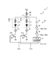
- FIG. 10 is a circuit diagram showing a configuration example of a light emitting device 1 and a light emitting element drive circuit 2 according to a modification 2 of the embodiment of the present disclosure, and is a drawing corresponding to FIG. 7 of the embodiment.
- one booster circuit 30 is common to a plurality of light emitting elements 3A and 3B connected in parallel between the power supply voltage Vcc and the ground potential. Connected to.
- the light emitting element 3A is interrupted by the signal S1a from the outside, and the light emitting element 3B is interrupted by the signal S1b from the outside. Then, these signals S1a and S1b are both input to the pulse generation circuit 34 of the second modification.
- the booster circuit 30 of the second modification can input both the signal S2a corresponding to the signal S1a and the signal S2b corresponding to the signal S1b to the inverter 32.
- the booster circuit 30 of the second modification can boost the node 33 at the timing when the light emitting element 3A emits light, and can boost the node 33 at the timing when the light emitting element 3B emits light.
- one booster circuit 30 can boost both the input side terminals of the plurality of light emitting elements 3A and 3B.
- one booster circuit 30 can be shared with the plurality of light emitting elements 3A and 3B, so that the chip area of the light emitting element drive circuit 2 can be reduced. Can be done.
- one booster circuit 30 is shared by two light emitting elements 3A and 3B, but the number of light emitting elements 3 sharing one booster circuit 30 is not limited to two.
- One booster circuit 30 may be shared by three or more light emitting elements 3.
- FIG. 11 is a circuit diagram showing a configuration example of a light emitting device 1 and a light emitting element drive circuit 2 according to a modification 3 of the embodiment of the present disclosure, and is a drawing corresponding to FIG. 1 of the embodiment.
- the light emitting element drive circuit 2 of the modification 3 has a circuit configuration of the constant current circuit 10 different from that of the embodiment.
- the constant current circuit 10 includes an N-type transistor 11A, an N-type transistor 12A, a constant current source 13, an N-type transistor 14, a capacitor 15, and an N-type transistor 16.
- the N-type transistor 11A and the N-type transistor 12A are provided in place of the N-type transistor 11 and the N-type transistor 12 of the embodiment.
- the N-type transistor 11A and the N-type transistor 12A are low withstand voltage transistors having substantially the same element characteristics and form a current mirror.
- the N-type transistor 16 separately added from the embodiment is a high withstand voltage transistor (for example, LDMOS), and is connected between the N-type transistor 11A and the light emitting element 3.
- LDMOS high withstand voltage transistor
- the drain of the N-type transistor 16 is connected to the terminal on the output side of the light emitting element 3, and the source of the N-type transistor 16 is connected to the drain of the N-type transistor 11A. Further, a voltage VL for logic operation is connected to the gate of the N-type transistor 14.
- the constant current circuit 10 of the modified example 3 can pass a constant current to the N-type transistor 11A based on the constant current flowing from the constant current source 13 to the N-type transistor 12.
- the constant current circuit 10 of the modification 3 can supply a constant current to the light emitting element 3 connected in series with the N-type transistor 11A.
- the high voltage transistor N-type transistor 16
- the power supply has a voltage higher than the voltage VL for logic.
- the voltage Vcc can be connected to the light emitting element 3. Therefore, according to the modification 3, the drive current of the light emitting element 3 can be increased.
- the number of high withstand voltage transistors that require a larger area than the low withstand voltage transistor in the constant current circuit 10 can be reduced (embodiment: 2, modified example 3: 1). Therefore, according to the modification 3, the chip area of the light emitting element drive circuit 2 can be reduced.
- the light emitting element drive circuit 2 includes a constant current circuit 10, a switch 20, and a booster circuit 30.
- the constant current circuit 10 supplies the constant current Ia to the light emitting element 3 from the power supply voltage Vcc.
- the switch 20 interrupts the current I1 flowing through the light emitting element 3 based on the external signal (signal S2).
- the booster circuit 30 boosts the voltage between the power supply voltage Vcc and the light emitting element 3 in synchronization with the timing at which the light emitting element 3 is turned on.
- the booster circuit 30 boosts the voltage between the power supply voltage Vcc and the light emitting element 3 from the time when the current I1 flowing through the light emitting element 3 rises until it becomes constant.
- the booster circuit 30 boosts the voltage between the power supply voltage Vcc and the light emitting element 3 from before the current I1 flowing through the light emitting element 3 falls to after the current I1 falls. To stop.
- the booster circuit 30 has a capacitor 31 and an inverter 32. Further, one terminal of the capacitor 31 is connected between the power supply voltage Vcc and the light emitting element 3, and the other terminal of the capacitor 31 is connected to the output terminal (node 32c) of the inverter 32.
- the terminal on the input side of the light emitting element 3 can be stably boosted.
- the constant current circuit 10 has a pair of high withstand voltage transistors (N-type transistors 11 and 12) constituting the current mirror.
- the drive current of the light emitting element 3 can be increased, and a stable constant current whose mirror ratio of the current mirror is close to the element size can be supplied to the light emitting element 3.
- the constant current circuit 10 has a pair of low withstand voltage transistors (N-type transistors 11A, 12A) constituting the current mirror. Further, the constant current circuit 10 has a high withstand voltage transistor (N-type transistor 16) connected between one of the low withstand voltage transistors and the light emitting element 3.
- the light emitting element drive circuit 2 has an assist switch 50 which is connected between the light emitting element 3 and the constant current circuit 10 and between the ground potential and conducts in synchronization with the boosting operation of the boosting circuit 30. Further prepare.
- the rise time of the light emitting element 3 can be further shortened.
- the light emitting element drive circuit 2 includes a plurality of light emitting elements 3, and the booster circuit 30 commonly boosts a plurality of light emitting elements 3 connected in parallel to the power supply voltage Vcc.
- the present technology can also have the following configurations.
- a constant current circuit that supplies a constant current to the light emitting element from the power supply voltage, A switch that interrupts the current flowing through the light emitting element based on an external signal, A booster circuit that boosts the voltage between the power supply voltage and the light emitting element in synchronization with the timing at which the light emitting element is turned on.
- a light emitting element drive circuit comprising.
- the booster circuit according to (1) or (2) wherein the booster circuit stops boosting between the power supply voltage and the light emitting element from before the current flowing through the light emitting element falls to after the current falls.
- the booster circuit has a capacitor and an inverter. One terminal of the capacitor is connected between the power supply voltage and the light emitting element, and the other terminal of the capacitor is connected to the output terminal of the inverter. Any one of (1) to (3).
- the light emitting element drive circuit according to. (5) The light emitting element drive circuit according to any one of (1) to (4) above, wherein the constant current circuit has a pair of high withstand voltage transistors constituting a current mirror.
- the constant current circuit has a pair of low withstand voltage transistors constituting a current mirror and a high withstand voltage transistor connected between one of the low withstand voltage transistors and the light emitting element.
- the light emitting element drive circuit according to any one. (7) Any one of (1) to (6) above, further comprising an assist switch connected between the light emitting element and the constant current circuit and between the ground potential and conducting in synchronization with the boosting operation of the boosting circuit.
- the light emitting element drive circuit according to 1.
- a plurality of the light emitting elements are provided.
- the light emitting element driving circuit according to any one of (1) to (7), wherein the boosting circuit commonly boosts a plurality of the light emitting elements connected in parallel with the power supply voltage.
- Light emitting element and A constant current circuit that supplies a constant current from the power supply voltage to the light emitting element, a switch that interrupts the current flowing through the light emitting element based on an external signal, and the power supply voltage in synchronization with the timing at which the light emitting element is lit.
- a light emitting element drive circuit having a booster circuit that boosts pressure between the light emitting element and the light emitting element.
- a light emitting device equipped with (10) The light emitting device according to (9), wherein the booster circuit boosts the voltage between the power supply voltage and the light emitting element from the time when the current flowing through the light emitting element rises until it becomes constant.
- the booster circuit has a capacitor and an inverter. One terminal of the capacitor is connected between the power supply voltage and the light emitting element, and the other terminal of the capacitor is connected to the output terminal of the inverter. Any one of (9) to (11).
- the light emitting device according to. (13) The light emitting device according to any one of (9) to (12) above, wherein the constant current circuit has a pair of high withstand voltage transistors constituting a current mirror.
- the constant current circuit has a pair of low withstand voltage transistors constituting a current mirror and a high withstand voltage transistor connected between one of the low withstand voltage transistors and the light emitting element.
- the light emitting device according to any one. (15) Any one of (9) to (14) above, further comprising an assist switch that is connected between the light emitting element and the constant current circuit and between the ground potential and conducts in synchronization with the boosting operation of the boosting circuit.
- the light emitting device according to one. (16) A plurality of the light emitting elements are provided.
Landscapes
- Physics & Mathematics (AREA)
- Condensed Matter Physics & Semiconductors (AREA)
- General Physics & Mathematics (AREA)
- Electromagnetism (AREA)
- Optics & Photonics (AREA)
- Led Devices (AREA)
- Circuit Arrangement For Electric Light Sources In General (AREA)
- Semiconductor Lasers (AREA)
Abstract
本開示に係る発光素子駆動回路(2)は、定電流回路(10)と、スイッチ(20)と、昇圧回路(30)とを備える。定電流回路(10)は、電源電圧(Vcc)から発光素子(3)に定電流(Ia)を供給する。スイッチ(20)は、外部信号に基づいて発光素子(3)に流れる電流(I1)を断続させる。昇圧回路(30)は、発光素子(3)が点灯するタイミングと同期して、電源電圧(Vcc)と発光素子(3)との間を昇圧する。
Description
本開示は、発光素子駆動回路および発光装置に関する。
レーザダイオード(Laser Diode:LD)やLED(Light Emitting Diode)などの発光素子を備える発光装置には、かかる発光素子に駆動電流を供給する発光素子駆動回路が設けられている(たとえば、特許文献1参照)。
本開示では、発光素子の立ち上がり時間の短縮と消費電力の低減とを両立させることができる発光素子駆動回路および発光装置を提案する。
本開示によれば、発光素子駆動回路が提供される。発光素子駆動回路は、定電流回路と、スイッチと、昇圧回路とを備える。定電流回路は、電源電圧から発光素子に定電流を供給する。スイッチは、外部信号に基づいて前記発光素子に流れる電流を断続させる。昇圧回路は、前記発光素子が点灯するタイミングと同期して、前記電源電圧と前記発光素子との間を昇圧する。
以下に、本開示の各実施形態について図面に基づいて詳細に説明する。なお、以下の各実施形態において、同一の部位には同一の符号を付することにより重複する説明を省略する。
レーザダイオード(Laser Diode:LD)やLED(Light Emitting Diode)などの発光素子を備える発光装置には、かかる発光素子に駆動電流を供給する発光素子駆動回路が設けられている。
また、この発光素子駆動回路において、発光素子を発光させる前から微弱な電流を流しておくことにより、発光素子が発光する際の立ち上がり時間を短縮する技術が知られている。
しかしながら、上記の技術では、発光素子が発光していない状態であっても発光素子に電流が流されていることから、発光装置の消費電力が増大してしまうという問題があった。
そこで、上述の問題点を克服し、発光素子の立ち上がり時間の短縮と消費電力の低減とを両立させることができる技術の実現が期待されている。
[発光装置および発光素子駆動回路の構成]
最初に、発光装置1および発光素子駆動回路2の具体的な構成について、図1を参照しながら説明する。図1は、本開示の実施形態に係る発光装置1および発光素子駆動回路2の構成例を示す回路図である。
最初に、発光装置1および発光素子駆動回路2の具体的な構成について、図1を参照しながら説明する。図1は、本開示の実施形態に係る発光装置1および発光素子駆動回路2の構成例を示す回路図である。
図1に示すように、発光装置1は、発光素子駆動回路2と、発光素子3とを備える。かかる発光装置1では、発光素子駆動回路2から発光素子3に駆動電流が供給されることにより、発光素子3が発光する。
発光素子3は、たとえば、レーザダイオードやLEDなどである。発光素子3は、発光素子駆動回路2から駆動電流が供給されることで発光するダイオード4と、寄生インダクタ5とを有する。そして、発光素子3の内部では、ダイオード4と寄生インダクタ5とが直列に接続される。
発光素子駆動回路2は、定電流回路10と、スイッチ20と、昇圧回路30と、インダクタ素子40とを備える。定電流回路10は、電源電圧Vccから発光素子3に所定の定電流を供給する。なお、電源電圧Vccは、発光素子3を発光可能な所定の電圧(たとえば、3.3(V)や5(V)など)である。
スイッチ20は、外部信号に基づいて、発光素子3に流れる電流を断続(切断または接続)させる。昇圧回路30は、発光素子3が点灯するタイミングと同期して、電源電圧Vccと発光素子3との間を昇圧する。インダクタ素子40は、電源電圧Vccと発光素子3との間に設けられる。
つづいて、発光装置1における各部の具体的な回路構成について説明する。発光素子3におけるダイオード4のアノードは、直列に接続された寄生インダクタ5およびインダクタ素子40を介して、電源電圧Vccに接続される。
また、ダイオード4のカソードは、直列に接続されたN型トランジスタ11およびスイッチ20を介して接地される。なお、N型トランジスタ11は定電流回路10の一部であり、スイッチ20はN型トランジスタで構成される。
定電流回路10は、N型トランジスタ11と、N型トランジスタ12と、定電流源13と、N型トランジスタ14と、コンデンサ15とを有する。N型トランジスタ11およびN型トランジスタ12は、略等しい素子特性を有する高耐圧トランジスタ(たとえば、LDMOS)であり、カレントミラーを構成する。
すなわち、N型トランジスタ11のゲートはN型トランジスタ12のゲートに接続され、N型トランジスタ12のゲートはN型トランジスタ12のドレインに接続される。
また、N型トランジスタ12のドレインは定電流源13を介してロジック動作用の電圧VLに接続され、N型トランジスタ12のソースはN型トランジスタ14を介して接地される。なお、ロジック動作用の電圧VLは、たとえば、1.8(V)である。
さらに、N型トランジスタ14のゲートにはロジック動作用の電圧VLが接続され、N型トランジスタ11のゲートおよびN型トランジスタ12のゲートはコンデンサ15を介して接地される。
このような回路構成によって、定電流回路10は、定電流源13からN型トランジスタ12に流される定電流に基づいて、N型トランジスタ11に定電流を流すことができる。これにより、定電流回路10は、N型トランジスタ11と直列に接続される発光素子3に対して、定電流を供給することができる。
なお、実施形態に係る定電流回路10では、N型トランジスタ11とN型トランジスタ12とが略等しい素子特性を有し、N型トランジスタ14はスイッチ20と略等しい素子特性を有するとよい。
これにより、実施形態に係る定電流回路10は、カレントミラーのミラー比が素子サイズに近い安定した定電流を発光素子3に供給することができる。
N型トランジスタで構成されるスイッチ20のドレインは、定電流回路10のN型トランジスタ11を介して発光素子3に接続され、スイッチ20のソースは接地される。また、スイッチ20のゲートには、図示しない制御部からの信号S1が入力される。かかる信号S1は、外部信号の一例である。
信号S1がハイレベルである場合、スイッチ20は導通状態となることから、電源電圧Vccから発光素子3に所定の定電流が供給され、発光素子3は点灯状態となる。一方で、信号S1がローレベルである場合、スイッチ20は切断状態となることから、電源電圧Vccから発光素子3には定電流が供給されず、発光素子3は消灯状態となる。
昇圧回路30は、コンデンサ31と、インバータ32とを有する。また、インバータ32は、P型トランジスタ32aとN型トランジスタ32bとを有する。
P型トランジスタ32aのソースはロジック動作用の電圧VLに接続され、P型トランジスタ32aのドレインは、ノード32cを介してN型トランジスタ32bのドレインに接続される。かかるノード32cは、インバータ32の出力端子に対応する。また、N型トランジスタ32bのソースは接地される。
そして、インバータ32の入力端子であるP型トランジスタ32aのゲートおよびN型トランジスタ32bのゲートには、別の外部信号である信号S2が入力される。かかる信号S2の詳細については後述する。
コンデンサ31は、インバータ32の出力端子であるノード32cと、電源電圧Vccおよび発光素子3の間(具体的には、インダクタ素子40および発光素子3の間)に設けられるノード33との間に設けられる。
[発光素子駆動回路の動作]
つづいて、実施形態に係る発光素子駆動回路2の動作について、図2~図8を参照しながら説明する。なお、以降においては、理解を容易にするため、実施形態と参考例1および参考例2とを比較しながら説明する。
つづいて、実施形態に係る発光素子駆動回路2の動作について、図2~図8を参照しながら説明する。なお、以降においては、理解を容易にするため、実施形態と参考例1および参考例2とを比較しながら説明する。
まず、本開示の参考例1について説明する。図2は、参考例1の発光装置1および発光素子駆動回路2の構成例を示す回路図である。図2に示すように、参考例1の発光装置1は、昇圧回路30が設けられない以外は実施形態と同様の構成である。
次に、図2に加えて図3を参照しながら、参考例1の発光素子駆動回路2の動作について説明する。図3は、参考例1の発光素子駆動回路2の動作例を示すタイミングチャートであり、電圧V1と、信号S1と、電圧V2と、電流I1とを示している。
ここで、図2に示すように、電圧V1は、発光素子3の入力側(すなわち、ダイオード4のアノード側)の電圧であり、信号S1はスイッチ20のゲートに入力される外部信号である。
また、電圧V2は、発光素子3の出力側(すなわち、ダイオード4のカソード側)の電圧であり、電流I1は、発光素子3の出力電流(すなわち、ダイオード4のカソードから出力される電流)である。
図3に示すように、初期状態において、信号S1はローレベルであることから、スイッチ20(図2参照)は切断状態である。したがって、初期状態では、発光素子3の出力電流(電流I1)がゼロであり、発光素子3は消灯状態である。
また、初期状態では、電流I1がゼロであることから、発光素子3の入力側の電圧V1および出力側の電圧V2は、ともに電源電圧Vccと略等しい値になる。
次に、時間T1において、信号S1がローレベルからハイレベルに切り替わると、スイッチ20が導通状態となるため、発光素子3に電流が流れ始める。これにより、時間T1から徐々に電流I1の値が上昇する。
また、時間T1において発光素子3内に電流が流れ始めると、発光素子3の入力側と出力側との間で電位差が生じることから、出力側の電圧V2が低下する。さらに、発光素子3内には寄生インダクタ5があることから、かかる寄生インダクタ5に流れる電流値の変化に起因して、発光素子3内で大きな電圧降下が生じる。
これにより、時間T1の後に、発光素子3の出力側の電圧V2は、接地電圧(図3ではGND)近傍の電圧Vaまで大きく低下する。
なお、この電圧V2は、カレントミラー回路である定電流回路10の出力電圧とみなすことができるが、このようにカレントミラー回路の出力電圧(電圧V2)が大きく低下した場合、定電流回路10のミラー比が維持できなくなる。
そして、定電流回路10のミラー比が崩れてしまうと、定電流回路10から発光素子3に必要な電流を流しにくくなることから、電流I1の上昇が抑制される。したがって、変形例1では、ようやく時間T2で電流I1は所定の定電流Iaに達する。
ここまで説明したように、変形例1では、発光素子3内の寄生インダクタ5に起因して発光素子3内で大きな電圧降下が生じることから、発光素子3の立ち上がり時間(図3ではT2-T1)を短縮することが困難である。
時間T2以降の流れについて説明する。時間T2において電流I1が所定の定電流Iaに達すると、寄生インダクタ5による電圧降下がなくなることから、発光素子3の出力側の電圧V2が上昇し、電圧Vbで一定となる。そして、発光素子3は、点灯状態を維持する。
次に、時間T3において、信号S1がハイレベルからローレベルに切り替わると、スイッチ20が切断状態となるため、発光素子3に流れる電流が低下し始める。これにより、時間T3から徐々に電流I1の値が減少する。
また、時間T3において発光素子3内の電流が減少し始めると、発光素子3の入力側と出力側との間の電位差が小さくなることから、出力側の電圧V2が上昇する。さらに、発光素子3内には寄生インダクタ5があることから、かかる寄生インダクタ5に流れる電流値の変化に起因して、発光素子3内で大きな電圧上昇が生じる。
これにより、時間T3の後に、発光素子3の出力側の電圧V2は、電源電圧Vccを超えた電圧Vdまで上昇する。
そして、時間T4で電流I1の値がゼロになると、発光素子3は消灯し、初期状態に戻る。また、時間T4において電流I1がゼロで一定になると、寄生インダクタ5による電圧上昇がなくなることから、発光素子3の出力側の電圧V2は電源電圧Vccと略等しい値に戻る。
つづいて、本開示の参考例2について説明する。図4は、参考例2の発光装置1および発光素子駆動回路2の構成例を示す回路図である。図4に示すように、参考例2の発光装置1は、昇圧回路30が設けられないことと、電源電圧がVccではなくVcc+VLであること以外は実施形態と同様の構成である。
次に、図4に加えて図5を参照しながら、参考例2の発光素子駆動回路2の動作について説明する。図5は、参考例2の発光素子駆動回路2の動作例を示すタイミングチャートであり、参考例1と同様に電圧V1と、信号S1と、電圧V2と、電流I1とを示している。
また、図5では、理解を容易にするため、参考例1における電圧V2および電流I1の変化を一点鎖線で示している。
図5に示すように、初期状態において、信号S1はローレベルであることから、スイッチ20(図4参照)は切断状態である。したがって、初期状態では、発光素子3の出力電流(電流I1)がゼロであり、発光素子3は消灯状態である。
また、初期状態では、電流I1がゼロであることから、発光素子3の入力側の電圧V1および出力側の電圧V2は、ともに電源電圧Vcc+VLと略等しい値となる。
次に、時間T1において、信号S1がローレベルからハイレベルに切り替わると、スイッチ20が導通状態となるため、発光素子3に電流が流れ始める。これにより、時間T1から徐々に電流I1の値が上昇する。
また、時間T1において発光素子3内に電流が流れ始めると、発光素子3の入力側と出力側との間で電位差が生じることから、出力側の電圧V2が低下する。また、変形例1と同様に、発光素子3内の寄生インダクタ5に流れる電流値の変化に起因して、発光素子3内で大きな電圧降下が生じる。
これにより、時間T1の後に、発光素子3の出力側の電圧V2は、電圧Va1まで大きく低下する。一方で、変形例2では、電源電圧自体をVcc+VLに昇圧していることから、電圧Va1の値は変形例1の電圧Vaよりも大きくなり、定電流回路10のミラー比が維持可能な値に維持される。
したがって、変形例2では、定電流回路10から発光素子3に必要な電流をより早く流すことができることから、電流I1の上昇が促進される。したがって、変形例2では、変形例1における時間T2よりも前の時間T2aで、電流I1は所定の定電流Iaに達する。
ここまで説明したように、変形例2では、電源電圧自体を昇圧することにより、発光素子3の立ち上がりの際にも定電流回路10のミラー比を維持できることから、発光素子3の立ち上がり時間(図5ではT2a-T1)を短縮することができる。
時間T2a以降の流れについて説明する。時間T2aにおいて電流I1が所定の定電流Iaに達すると、寄生インダクタ5による電圧降下がなくなることから、発光素子3の出力側の電圧V2が上昇し、電圧Vb1で一定となる。そして、発光素子3は、点灯状態を維持する。
なお、かかる電圧Vb1は、電源電圧自体が昇圧されていることから、変形例1における電圧Vbよりも大きい値となる。
次に、時間T3において、信号S1がハイレベルからローレベルに切り替わると、スイッチ20が切断状態となるため、発光素子3に流れる電流が低下し始める。これにより、時間T3から徐々に電流I1の値が減少する。
また、時間T3において発光素子3内の電流が減少し始めると、発光素子3の入力側と出力側との間の電位差が小さくなることから、出力側の電圧V2が上昇する。さらに、発光素子3内には寄生インダクタ5があることから、かかる寄生インダクタ5に流れる電流値の変化に起因して、発光素子3内で大きな電圧上昇が生じる。
これにより、時間T3の後に、発光素子3の出力側の電圧V2は、電源電圧Vcc+VLを超えた電圧Vd1まで上昇する。
そして、時間T4で電流I1の値がゼロになると、発光素子3は消灯し、初期状態に戻る。また、時間T4において電流I1がゼロで一定になると、寄生インダクタ5による電圧上昇がなくなることから、発光素子3の出力側の電圧V2は電源電圧Vcc+VLと略等しい値に戻る。
ここで、変形例2では、電流I1が所定の定電流Iaに達した時間T2aから時間T3までの間、電圧V2の値が変形例1よりも大きい電圧Vb1となる。これにより、発光装置1内の損失が大きくなることから、発光装置1の消費電力が増大してしまう。
つづいて、図1および図6を参照しながら、実施形態に係る発光素子駆動回路2の動作について説明する。図6は、本開示の実施形態に係る発光素子駆動回路2の動作例を示すタイミングチャートであり、電圧V1、信号S1、電圧V2および電流I1に加えて、信号S2も示している。
ここで、図1に示すように、信号S2は、昇圧回路30におけるインバータ32の入力端子に入力される外部信号である。また、図6では、理解を容易にするため、参考例2における電圧V2の変化を二点鎖線で示している。
図6に示すように、初期状態において、信号S1はローレベルであることから、スイッチ20(図1参照)は切断状態である。したがって、初期状態では、発光素子3の出力電流(電流I1)がゼロであり、発光素子3は消灯状態である。
また、初期状態では、電流I1がゼロであることから、発光素子3の入力側の電圧V1および出力側の電圧V2は、ともに電源電圧Vccと略等しい値となる。
さらに、初期状態では、信号S2がハイレベルであることから、P型トランジスタ32aは切断状態となり、N型トランジスタ32bは導通状態となる。これにより、コンデンサ31の両方の端子にはそれぞれ電源電圧Vccおよび接地電圧が印加され、両方の端子の電位差が電源電圧Vccと略等しい値になるようにコンデンサ31が充電される。
次に、時間T1において、信号S1がローレベルからハイレベルに切り替わると、スイッチ20が導通状態となるため、発光素子3に電流が流れ始める。これにより、時間T1から徐々に電流I1の値が上昇する。
また、時間T1では、信号S1と同期して、信号S2がハイレベルからローレベルに切り替わる。これにより、P型トランジスタ32aは導通状態となり、N型トランジスタ32bは切断状態となることから、インバータ32の出力端子(ノード32c)の電圧がゼロから電圧VLに変化する。
これにより、インバータ32の出力端子(ノード32c)の電圧VLがコンデンサ31の両方の端子の電位差(電圧Vcc)と足し合わされ、ノード33の電圧(すなわち、発光素子3の入力側の電圧V1)がVcc+VLに昇圧される。
すなわち、実施形態では、発光素子3が点灯するタイミング(時間T1)と同期して、ノード33の電圧を昇圧回路30で昇圧する。
そして、時間T1において発光素子3内に電流が流れ始めると、発光素子3の入力側と出力側との間で電位差が生じることから、出力側の電圧V2が低下する。また、変形例2と同様に、発光素子3内の寄生インダクタ5に流れる電流値の変化に起因して、発光素子3内で大きな電圧降下が生じる。
これにより、時間T1の後に、発光素子3の出力側の電圧V2は、電圧Va1まで大きく低下する。一方で、実施形態では、発光素子3の入力側の端子(電圧V1)を昇圧していることから、変形例2と同様に、電圧V2の値は、定電流回路10のミラー比が維持可能な値(電圧Va1)に維持される。
したがって、実施形態では、定電流回路10から発光素子3に必要な電流をより早く流すことができることから、電流I1の上昇が促進され、変形例2と同様の時間T2aで、電流I1は所定の定電流Iaに達する。
ここまで説明したように、実施形態では、昇圧回路30で発光素子3の入力側の端子を昇圧することで、発光素子3の立ち上がりの際にも定電流回路10のより早くミラー比の電流を流すことができることから、発光素子3の立ち上がり時間(T2a-T1)を短縮することができる。
時間T2a以降の流れについて説明する。時間T2aにおいて電流I1が所定の定電流Iaに達すると、寄生インダクタ5による電圧降下がなくなることから、発光素子3の出力側の電圧V2が上昇し、電圧Vb1で一定となる。そして、発光素子3は、点灯状態を維持する。
ここで、実施形態では、時間T2aよりも後の時間T2bにおいて、信号S2がローレベルからハイレベルに切り替わる。これにより、インバータ32の出力端子(ノード32c)の電圧が電圧VLからゼロに変化することから、ノード33がコンデンサ31によって昇圧されなくなる。
すなわち、実施形態では、時間T2bで発光素子3の入力側の電圧V1が電源電圧Vccと略等しい値に戻る。これにより、発光素子3の出力側の電圧V2も、時間T2bで電圧Vb1から変形例1と同様の電圧Vbに低下する。
次に、時間T3において、信号S1がハイレベルからローレベルに切り替わると、スイッチ20が切断状態となるため、発光素子3に流れる電流が低下し始める。これにより、時間T3から徐々に電流I1の値が減少する。以降は上述の変形例1と同様であるため、説明を省略する。
ここで、実施形態では、時間T2bから時間T3までの間、電圧V2の値を変形例2よりも小さい電圧Vbに低減することができる。これにより、発光装置1内の損失を小さくすることができることから、発光装置1の消費電力を低減することができる。
ここまで説明したように、実施形態では、発光素子3が点灯するタイミングと同期して、昇圧回路30により発光素子3の入力側の端子を昇圧することにより、発光素子3の立ち上がり時間の短縮と消費電力の低減とを両立させることができる。
また、実施形態では、コンデンサ31およびインバータ32を用いて昇圧回路30を構成することにより、発光素子3の入力側の端子を安定して昇圧することができる。
なお、実施形態において、昇圧回路30は、必ずしもコンデンサ31およびインバータ32を用いて構成する必要はなく、その他の既知の昇圧回路を用いて発光素子3の入力側の端子を昇圧してもよい。
また、実施形態では、一対の高耐圧トランジスタ(N型トランジスタ11およびN型トランジスタ12)でカレントミラーを構成することにより、ロジック用の電圧VLよりも高電圧である電源電圧Vccを発光素子3に接続することができる。
したがって、実施形態によれば、発光素子3の駆動電流を大きくすることができる。さらに、実施形態では、素子特性が略等しい一対の高耐圧トランジスタでカレントミラーを構成することから、カレントミラーのミラー比が素子サイズに近い安定した定電流を発光素子3に供給することができる。
また、実施形態では、昇圧回路30が、少なくとも発光素子3を流れる電流I1が立ち上がってから一定になるまでの間(すなわち、少なくとも時間T1から時間T2aまでの間)、ノード33を昇圧するとよい。
もし仮に、電流I1が立ち上がっている最中に(すなわち、時間T2aよりも前に)ノード33の昇圧を停止すると、発光素子3の出力側の電圧V2が低下してしまうことから、定電流回路10のミラー比が維持できなくなる恐れがある。
そしてこの場合、定電流回路10から発光素子3に必要な電流を流しにくくなることから、電流I1の上昇が抑制され、電流I1が所定の定電流Iaに達するまでの時間が長くかかってしまう。
しかしながら、実施形態では、少なくとも時間T1から時間T2aまでの間ノード33を昇圧することから、電流I1が所定の定電流Iaに達するまでの時間が長くなることを抑制することができる。
また、実施形態では、昇圧回路30が、発光素子3を流れる電流I1が立ち下がる前から立ち下がった後までの間(すなわち、少なくとも時間T3よりも前から時間T4の後までの間)、ノード33の昇圧を停止するとよい。
もし仮に、電流I1が立ち下がり始めた後から(すなわち、時間T3よりも後から)ノード33の昇圧を停止した場合、時間T2aから時間T3までの間はノード33が昇圧されていたことになる。
そしてこの場合、発光素子3に定電流Iaが流れ、発光素子3の消費電力が最も大きい時間T2aから時間T3までの間は、電圧V2が電圧Vb1で維持されることから、発光装置1内の損失が大きくなり、発光装置1の消費電力が増大してしまう。
しかしながら、実施形態では、少なくとも時間T3よりも前にノード33の昇圧を停止することから、発光装置1における消費電力の増大を抑制することができる。
なお、実施形態では、発光素子3が立ち上がった時間T2aの後、速やかにノード33の昇圧を停止するとよい。たとえば、発光素子3の立ち上がり時間をTrとした場合、信号S2の幅(すなわち、時間T1から時間T2bまでの時間)を1.1Tr~1.5Trの範囲にするとよい。これにより、発光装置1における消費電力の増大を効果的に抑制することができる。
ここまで説明した昇圧回路30による昇圧のタイミングは、信号S2により制御される。そこで、かかる信号S2の生成方法の一例について、図7および図8を参照しながら説明する。
図7は、本開示の実施形態に係る発光装置1および発光素子駆動回路2の構成例を示す回路図であり、信号S2の生成回路についての詳細を示した図である。なお、図7では、定電流回路10を定電流源として1つの記号で記載している。
図7の例では、昇圧回路30が、上述のコンデンサ31とインバータ32とに加えて、パルス生成回路34と、インバータ35とを有する。
パルス生成回路34は、所定の幅を有するパルス信号を生成する。パルス生成回路34は、たとえば、図示しないエッジ検出回路および遅延回路を内部に有し、入力信号の立ち上がりエッジと同期した立ち上がりのパルス信号を生成する。また、パルス生成回路34は、内部の遅延回路において予め設定された遅延時間に基づいた幅のパルス信号を生成する。
図7に示すように、図示しない制御部から信号S1がスイッチ20のゲートに入力され、かかるスイッチ20の断続が制御される。また、かかる信号S1は、パルス生成回路34にも入力される。
そして、パルス生成回路34は、入力された信号S1に基づいて、信号S2xをインバータ35に出力する。かかる信号S2xは、図8に示すように、信号S1と同じ立ち上がりタイミング(ここでは時間T1)であり、時間T1から時間T2bまでの幅を有するパルス信号である。図8は、本開示の実施形態に係る各信号の動作例を示すタイミングチャートである。
そして、図7に示すように、信号S2xが入力されたインバータ35は、かかる信号S2xを反転させた信号S2(図8参照)をインバータ32に出力する。
このように、信号S1に基づいて信号S2を生成することにより、発光素子3の立ち上がりと昇圧回路30とを精度よく同期させることができる。なお、図7の例はあくまで一例であり、パルス生成回路34およびインバータ35以外の回路を用いて、信号S1から信号S2を生成してもよい。
また、上記の実施形態では、P型トランジスタ32aのソースをロジック用の電圧VLに接続することにより、かかる電圧VLだけ昇圧回路30で昇圧する例について示したが、昇圧回路30で昇圧可能な電圧はかかる電圧VLに限られない。
たとえば、P型トランジスタ32aのソースを電源電圧Vccに接続してもよいし、その他の電圧源にP型トランジスタ32aのソースを接続してもよい。
[各種変形例]
つづいて、実施形態の各種変形例について、図9~図11を参照しながら説明する。図9は、本開示の実施形態の変形例1に係る発光装置1および発光素子駆動回路2の構成例を示す回路図であり、実施形態の図7に対応する図面である。
つづいて、実施形態の各種変形例について、図9~図11を参照しながら説明する。図9は、本開示の実施形態の変形例1に係る発光装置1および発光素子駆動回路2の構成例を示す回路図であり、実施形態の図7に対応する図面である。
図9に示すように、変形例1の発光素子駆動回路2は、アシストスイッチ50が設けられる点が実施形態と異なる。かかるアシストスイッチ50は、発光素子3および定電流回路10の間と、接地電位との間に接続される。すなわち、アシストスイッチ50は、発光素子3の出力側の端子と接地電位との間に接続される。
また、アシストスイッチ50は、パルス生成回路34から出力される信号S2xに基づいて断続される。すなわち、アシストスイッチ50は、昇圧回路30の昇圧動作と同期して導通する。たとえば、アシストスイッチ50はN型トランジスタであり、かかるN型トランジスタのゲートに信号S2xが入力される。
この変形例1では、昇圧回路30の昇圧動作と同期してアシストスイッチ50を導通させることで、発光素子3の出力側の電圧V2が低下して定電流回路10の動作が弱った際に、アシストスイッチ50のオン抵抗で定電流回路10の動作を補助することができる。
したがって、変形例1によれば、電流I1の上昇がさらに促進されることから、発光素子3の立ち上がり時間をさらに短縮することができる。
図10は、本開示の実施形態の変形例2に係る発光装置1および発光素子駆動回路2の構成例を示す回路図であり、実施形態の図7に対応する図面である。
図10に示すように、変形例2の発光素子駆動回路2は、電源電圧Vccから接地電位の間に並列に接続される複数の発光素子3A、3Bに対して、1つの昇圧回路30が共通に接続される。
この変形例2では、発光素子3Aが外部からの信号S1aにより断続され、発光素子3Bが外部からの信号S1bにより断続される。そして、変形例2のパルス生成回路34には、これらの信号S1a、S1bがともに入力される。
これにより、変形例2の昇圧回路30は、信号S1aに応じた信号S2aと、信号S1bに応じた信号S2bとを両方インバータ32に入力することができる。
すなわち、変形例2の昇圧回路30は、発光素子3Aが発光するタイミングでノード33を昇圧することができるとともに、発光素子3Bが発光するタイミングでノード33を昇圧することができる。
したがって、変形例2によれば、1つの昇圧回路30で複数の発光素子3A、3Bの入力側の端子をともに昇圧することができる。
このように、変形例2の発光素子駆動回路2では、複数の発光素子3A、3Bに対して1つの昇圧回路30を共有することができることから、発光素子駆動回路2のチップ面積を低減することができる。
なお、図10の例では、1つの昇圧回路30を2つの発光素子3A、3Bで共有した例について示したが、1つの昇圧回路30を共有する発光素子3の数は2つに限られず、3つ以上の発光素子3で1つの昇圧回路30を共有してもよい。
図11は、本開示の実施形態の変形例3に係る発光装置1および発光素子駆動回路2の構成例を示す回路図であり、実施形態の図1に対応する図面である。図11に示すように、変形例3の発光素子駆動回路2は、定電流回路10の回路構成が実施形態と異なる。
図11に示すように、定電流回路10は、N型トランジスタ11Aと、N型トランジスタ12Aと、定電流源13と、N型トランジスタ14と、コンデンサ15と、N型トランジスタ16とを有する。
N型トランジスタ11AおよびN型トランジスタ12Aは、実施形態のN型トランジスタ11およびN型トランジスタ12と入れ替わって設けられる。N型トランジスタ11AおよびN型トランジスタ12Aは、略等しい素子特性を有する低耐圧トランジスタであり、カレントミラーを構成する。
また、実施形態から別途追加されるN型トランジスタ16は、高耐圧トランジスタ(たとえば、LDMOS)であり、N型トランジスタ11Aと発光素子3との間に接続される。
すなわち、N型トランジスタ16のドレインは発光素子3の出力側の端子に接続され、N型トランジスタ16のソースはN型トランジスタ11Aのドレインに接続される。また、N型トランジスタ14のゲートにはロジック動作用の電圧VLが接続される。
このような回路構成によって、変形例3の定電流回路10は、定電流源13からN型トランジスタ12に流される定電流に基づいて、N型トランジスタ11Aに定電流を流すことができる。これにより、変形例3の定電流回路10は、N型トランジスタ11Aと直列に接続される発光素子3に対して、定電流を供給することができる。
また、変形例3の定電流回路10は、発光素子3の出力側の端子に高耐圧トランジスタ(N型トランジスタ16)が接続されることから、ロジック用の電圧VLよりも高電圧である電源電圧Vccを発光素子3に接続することができる。したがって、変形例3によれば、発光素子3の駆動電流を大きくすることができる。
さらに、変形例3では、定電流回路10において、低耐圧トランジスタに比べて大きな面積が必要となる高耐圧トランジスタの数を減らすことができる(実施形態:2個、変形例3:1個)。したがって、変形例3によれば、発光素子駆動回路2のチップ面積を低減することができる。
なお、変形例3の定電流回路10において、N型トランジスタ12Aに接続される電圧は電源電圧Vccではなくロジック用の電圧VLであることから、N型トランジスタ12Aに低耐圧トランジスタを用いたとしても特に支障は無い。
[効果]
実施形態に係る発光素子駆動回路2は、定電流回路10と、スイッチ20と、昇圧回路30とを備える。定電流回路10は、電源電圧Vccから発光素子3に定電流Iaを供給する。スイッチ20は、外部信号(信号S2)に基づいて発光素子3に流れる電流I1を断続させる。昇圧回路30は、発光素子3が点灯するタイミングと同期して、電源電圧Vccと発光素子3との間を昇圧する。
実施形態に係る発光素子駆動回路2は、定電流回路10と、スイッチ20と、昇圧回路30とを備える。定電流回路10は、電源電圧Vccから発光素子3に定電流Iaを供給する。スイッチ20は、外部信号(信号S2)に基づいて発光素子3に流れる電流I1を断続させる。昇圧回路30は、発光素子3が点灯するタイミングと同期して、電源電圧Vccと発光素子3との間を昇圧する。
これにより、発光素子3の立ち上がり時間の短縮と消費電力の低減とを両立させることができる。
また、実施形態に係る発光素子駆動回路2において、昇圧回路30は、発光素子3を流れる電流I1が立ち上がってから一定になるまでの間、電源電圧Vccと発光素子3との間を昇圧する。
これにより、発光素子3を流れる電流I1が所定の定電流Iaに達するまでの時間が長くなることを抑制することができる。
また、実施形態に係る発光素子駆動回路2において、昇圧回路30は、発光素子3を流れる電流I1が立ち下がる前から立ち下がった後までの間、電源電圧Vccと発光素子3との間の昇圧を停止する。
これにより、発光装置1における消費電力の増大を抑制することができる。
また、実施形態に係る発光素子駆動回路2において、昇圧回路30は、コンデンサ31およびインバータ32を有する。また、コンデンサ31の一方の端子が電源電圧Vccと発光素子3との間に接続され、コンデンサ31の他方の端子がインバータ32の出力端子(ノード32c)に接続される。
これにより、発光素子3の入力側の端子を安定して昇圧することができる。
また、実施形態に係る発光素子駆動回路2において、定電流回路10は、カレントミラーを構成する一対の高耐圧トランジスタ(N型トランジスタ11、12)を有する。
これにより、発光素子3の駆動電流を大きくすることができるとともに、カレントミラーのミラー比が素子サイズに近い安定した定電流を発光素子3に供給することができる。
また、実施形態に係る発光素子駆動回路2において、定電流回路10は、カレントミラーを構成する一対の低耐圧トランジスタ(N型トランジスタ11A、12A)を有する。また、定電流回路10は、低耐圧トランジスタの一方と発光素子3との間に接続される高耐圧トランジスタ(N型トランジスタ16)を有する。
これにより、発光素子駆動回路2のチップ面積を低減することができる。
また、実施形態に係る発光素子駆動回路2は、発光素子3および定電流回路10の間と、接地電位との間に接続され、昇圧回路30の昇圧動作と同期して導通するアシストスイッチ50をさらに備える。
これにより、発光素子3の立ち上がり時間をさらに短縮することができる。
また、実施形態に係る発光素子駆動回路2は、発光素子3を複数備え、昇圧回路30は、電源電圧Vccに並列に接続される複数の発光素子3を共通に昇圧する。
これにより、発光素子駆動回路2のチップ面積を低減することができる。
以上、本開示の実施形態について説明したが、本開示の技術的範囲は、上述の実施形態そのままに限定されるものではなく、本開示の要旨を逸脱しない範囲において種々の変更が可能である。また、異なる実施形態及び変形例にわたる構成要素を適宜組み合わせてもよい。
また、本明細書に記載された効果はあくまで例示であって限定されるものでは無く、また他の効果があってもよい。
なお、本技術は以下のような構成も取ることができる。
(1)
電源電圧から発光素子に定電流を供給する定電流回路と、
外部信号に基づいて前記発光素子を流れる電流を断続させるスイッチと、
前記発光素子が点灯するタイミングと同期して、前記電源電圧と前記発光素子との間を昇圧する昇圧回路と、
を備える発光素子駆動回路。
(2)
前記昇圧回路は、前記発光素子を流れる電流が立ち上がってから一定になるまでの間、前記電源電圧と前記発光素子との間を昇圧する
前記(1)に記載の発光素子駆動回路。
(3)
前記昇圧回路は、前記発光素子を流れる電流が立ち下がる前から立ち下がった後までの間、前記電源電圧と前記発光素子との間の昇圧を停止する
前記(1)または(2)に記載の発光素子駆動回路。
(4)
前記昇圧回路は、コンデンサおよびインバータを有し、
前記コンデンサの一方の端子が前記電源電圧と前記発光素子との間に接続され、前記コンデンサの他方の端子が前記インバータの出力端子に接続される
前記(1)~(3)のいずれか一つに記載の発光素子駆動回路。
(5)
前記定電流回路は、カレントミラーを構成する一対の高耐圧トランジスタを有する
前記(1)~(4)のいずれか一つに記載の発光素子駆動回路。
(6)
前記定電流回路は、カレントミラーを構成する一対の低耐圧トランジスタと、前記低耐圧トランジスタの一方と前記発光素子との間に接続される高耐圧トランジスタとを有する
前記(1)~(4)のいずれか一つに記載の発光素子駆動回路。
(7)
前記発光素子および前記定電流回路の間と、接地電位との間に接続され、前記昇圧回路の昇圧動作と同期して導通するアシストスイッチをさらに備える
前記(1)~(6)のいずれか一つに記載の発光素子駆動回路。
(8)
前記発光素子を複数備え、
前記昇圧回路は、前記電源電圧に並列に接続される複数の前記発光素子を共通に昇圧する
前記(1)~(7)のいずれか一つに記載の発光素子駆動回路。
(9)
発光素子と、
電源電圧から前記発光素子に定電流を供給する定電流回路と、外部信号に基づいて前記発光素子に流れる電流を断続させるスイッチと、前記発光素子が点灯するタイミングと同期して、前記電源電圧と前記発光素子との間を昇圧する昇圧回路と、を有する発光素子駆動回路と、
を備える発光装置。
(10)
前記昇圧回路は、前記発光素子を流れる電流が立ち上がってから一定になるまでの間、前記電源電圧と前記発光素子との間を昇圧する
前記(9)に記載の発光装置。
(11)
前記昇圧回路は、前記発光素子を流れる電流が立ち下がる前から立ち下がった後までの間、前記電源電圧と前記発光素子との間の昇圧を停止する
前記(9)または(10)に記載の発光装置。
(12)
前記昇圧回路は、コンデンサおよびインバータを有し、
前記コンデンサの一方の端子が前記電源電圧と前記発光素子との間に接続され、前記コンデンサの他方の端子が前記インバータの出力端子に接続される
前記(9)~(11)のいずれか一つに記載の発光装置。
(13)
前記定電流回路は、カレントミラーを構成する一対の高耐圧トランジスタを有する
前記(9)~(12)のいずれか一つに記載の発光装置。
(14)
前記定電流回路は、カレントミラーを構成する一対の低耐圧トランジスタと、前記低耐圧トランジスタの一方と前記発光素子との間に接続される高耐圧トランジスタとを有する
前記(9)~(12)のいずれか一つに記載の発光装置。
(15)
前記発光素子および前記定電流回路の間と、接地電位との間に接続され、前記昇圧回路の昇圧動作と同期して導通するアシストスイッチをさらに備える
前記(9)~(14)のいずれか一つに記載の発光装置。
(16)
前記発光素子を複数備え、
前記昇圧回路は、前記電源電圧に並列に接続される複数の前記発光素子を共通に昇圧する
前記(9)~(15)のいずれか一つに記載の発光装置。
(1)
電源電圧から発光素子に定電流を供給する定電流回路と、
外部信号に基づいて前記発光素子を流れる電流を断続させるスイッチと、
前記発光素子が点灯するタイミングと同期して、前記電源電圧と前記発光素子との間を昇圧する昇圧回路と、
を備える発光素子駆動回路。
(2)
前記昇圧回路は、前記発光素子を流れる電流が立ち上がってから一定になるまでの間、前記電源電圧と前記発光素子との間を昇圧する
前記(1)に記載の発光素子駆動回路。
(3)
前記昇圧回路は、前記発光素子を流れる電流が立ち下がる前から立ち下がった後までの間、前記電源電圧と前記発光素子との間の昇圧を停止する
前記(1)または(2)に記載の発光素子駆動回路。
(4)
前記昇圧回路は、コンデンサおよびインバータを有し、
前記コンデンサの一方の端子が前記電源電圧と前記発光素子との間に接続され、前記コンデンサの他方の端子が前記インバータの出力端子に接続される
前記(1)~(3)のいずれか一つに記載の発光素子駆動回路。
(5)
前記定電流回路は、カレントミラーを構成する一対の高耐圧トランジスタを有する
前記(1)~(4)のいずれか一つに記載の発光素子駆動回路。
(6)
前記定電流回路は、カレントミラーを構成する一対の低耐圧トランジスタと、前記低耐圧トランジスタの一方と前記発光素子との間に接続される高耐圧トランジスタとを有する
前記(1)~(4)のいずれか一つに記載の発光素子駆動回路。
(7)
前記発光素子および前記定電流回路の間と、接地電位との間に接続され、前記昇圧回路の昇圧動作と同期して導通するアシストスイッチをさらに備える
前記(1)~(6)のいずれか一つに記載の発光素子駆動回路。
(8)
前記発光素子を複数備え、
前記昇圧回路は、前記電源電圧に並列に接続される複数の前記発光素子を共通に昇圧する
前記(1)~(7)のいずれか一つに記載の発光素子駆動回路。
(9)
発光素子と、
電源電圧から前記発光素子に定電流を供給する定電流回路と、外部信号に基づいて前記発光素子に流れる電流を断続させるスイッチと、前記発光素子が点灯するタイミングと同期して、前記電源電圧と前記発光素子との間を昇圧する昇圧回路と、を有する発光素子駆動回路と、
を備える発光装置。
(10)
前記昇圧回路は、前記発光素子を流れる電流が立ち上がってから一定になるまでの間、前記電源電圧と前記発光素子との間を昇圧する
前記(9)に記載の発光装置。
(11)
前記昇圧回路は、前記発光素子を流れる電流が立ち下がる前から立ち下がった後までの間、前記電源電圧と前記発光素子との間の昇圧を停止する
前記(9)または(10)に記載の発光装置。
(12)
前記昇圧回路は、コンデンサおよびインバータを有し、
前記コンデンサの一方の端子が前記電源電圧と前記発光素子との間に接続され、前記コンデンサの他方の端子が前記インバータの出力端子に接続される
前記(9)~(11)のいずれか一つに記載の発光装置。
(13)
前記定電流回路は、カレントミラーを構成する一対の高耐圧トランジスタを有する
前記(9)~(12)のいずれか一つに記載の発光装置。
(14)
前記定電流回路は、カレントミラーを構成する一対の低耐圧トランジスタと、前記低耐圧トランジスタの一方と前記発光素子との間に接続される高耐圧トランジスタとを有する
前記(9)~(12)のいずれか一つに記載の発光装置。
(15)
前記発光素子および前記定電流回路の間と、接地電位との間に接続され、前記昇圧回路の昇圧動作と同期して導通するアシストスイッチをさらに備える
前記(9)~(14)のいずれか一つに記載の発光装置。
(16)
前記発光素子を複数備え、
前記昇圧回路は、前記電源電圧に並列に接続される複数の前記発光素子を共通に昇圧する
前記(9)~(15)のいずれか一つに記載の発光装置。
1 発光装置
2 発光素子駆動回路
3 発光素子
4 ダイオード
5 寄生インダクタ
10 定電流回路
20 スイッチ
30 昇圧回路
31 コンデンサ
32 インバータ
40 インダクタ素子
50 アシストスイッチ
I1 電流
S1 信号(外部信号の一例)
2 発光素子駆動回路
3 発光素子
4 ダイオード
5 寄生インダクタ
10 定電流回路
20 スイッチ
30 昇圧回路
31 コンデンサ
32 インバータ
40 インダクタ素子
50 アシストスイッチ
I1 電流
S1 信号(外部信号の一例)
Claims (9)
- 電源電圧から発光素子に定電流を供給する定電流回路と、
外部信号に基づいて前記発光素子を流れる電流を断続させるスイッチと、
前記発光素子が点灯するタイミングと同期して、前記電源電圧と前記発光素子との間を昇圧する昇圧回路と、
を備える発光素子駆動回路。 - 前記昇圧回路は、前記発光素子を流れる電流が立ち上がってから一定になるまでの間、前記電源電圧と前記発光素子との間を昇圧する
請求項1に記載の発光素子駆動回路。 - 前記昇圧回路は、前記発光素子を流れる電流が立ち下がる前から立ち下がった後までの間、前記電源電圧と前記発光素子との間の昇圧を停止する
請求項1に記載の発光素子駆動回路。 - 前記昇圧回路は、コンデンサおよびインバータを有し、
前記コンデンサの一方の端子が前記電源電圧と前記発光素子との間に接続され、前記コンデンサの他方の端子が前記インバータの出力端子に接続される
請求項1に記載の発光素子駆動回路。 - 前記定電流回路は、カレントミラーを構成する一対の高耐圧トランジスタを有する
請求項1に記載の発光素子駆動回路。 - 前記定電流回路は、カレントミラーを構成する一対の低耐圧トランジスタと、前記低耐圧トランジスタの一方と前記発光素子との間に接続される高耐圧トランジスタとを有する
請求項1に記載の発光素子駆動回路。 - 前記発光素子および前記定電流回路の間と、接地電位との間に接続され、前記昇圧回路の昇圧動作と同期して導通するアシストスイッチをさらに備える
請求項1に記載の発光素子駆動回路。 - 前記発光素子を複数備え、
前記昇圧回路は、前記電源電圧に並列に接続される複数の前記発光素子を共通に昇圧する
請求項1に記載の発光素子駆動回路。 - 発光素子と、
電源電圧から前記発光素子に定電流を供給する定電流回路と、外部信号に基づいて前記発光素子に流れる電流を断続させるスイッチと、前記発光素子が点灯するタイミングと同期して、前記電源電圧と前記発光素子との間を昇圧する昇圧回路と、を有する発光素子駆動回路と、
を備える発光装置。
Priority Applications (2)
| Application Number | Priority Date | Filing Date | Title |
|---|---|---|---|
| US17/772,346 US20220408528A1 (en) | 2019-11-19 | 2020-11-09 | Light emitting element driving circuit and light emitting device |
| CN202080078634.2A CN114731023A (zh) | 2019-11-19 | 2020-11-09 | 发光元件驱动电路和发光装置 |
Applications Claiming Priority (2)
| Application Number | Priority Date | Filing Date | Title |
|---|---|---|---|
| JP2019208755A JP2021082699A (ja) | 2019-11-19 | 2019-11-19 | 発光素子駆動回路および発光装置 |
| JP2019-208755 | 2019-11-19 |
Publications (1)
| Publication Number | Publication Date |
|---|---|
| WO2021100526A1 true WO2021100526A1 (ja) | 2021-05-27 |
Family
ID=75965999
Family Applications (1)
| Application Number | Title | Priority Date | Filing Date |
|---|---|---|---|
| PCT/JP2020/041781 Ceased WO2021100526A1 (ja) | 2019-11-19 | 2020-11-09 | 発光素子駆動回路および発光装置 |
Country Status (4)
| Country | Link |
|---|---|
| US (1) | US20220408528A1 (ja) |
| JP (1) | JP2021082699A (ja) |
| CN (1) | CN114731023A (ja) |
| WO (1) | WO2021100526A1 (ja) |
Families Citing this family (2)
| Publication number | Priority date | Publication date | Assignee | Title |
|---|---|---|---|---|
| CN114299870A (zh) * | 2022-02-14 | 2022-04-08 | Tcl华星光电技术有限公司 | 驱动电路及显示面板 |
| JP2024137258A (ja) * | 2023-03-24 | 2024-10-07 | ソニーセミコンダクタソリューションズ株式会社 | 光源駆動装置及び測距システム |
Citations (4)
| Publication number | Priority date | Publication date | Assignee | Title |
|---|---|---|---|---|
| JP2009231644A (ja) * | 2008-03-25 | 2009-10-08 | Panasonic Corp | 発光素子駆動回路 |
| JP2011108799A (ja) * | 2009-11-17 | 2011-06-02 | Sharp Corp | 発光装置、並びに、当該発光装置を備えた照明装置及び表示装置 |
| JP2012151057A (ja) * | 2011-01-21 | 2012-08-09 | Sony Corp | 発光素子駆動回路、発光装置、表示装置、および発光制御方法 |
| JP2012204301A (ja) * | 2011-03-28 | 2012-10-22 | Funai Electric Co Ltd | 点灯制御回路、及び、表示装置 |
Family Cites Families (1)
| Publication number | Priority date | Publication date | Assignee | Title |
|---|---|---|---|---|
| JP4376385B2 (ja) * | 1999-11-15 | 2009-12-02 | 富士通株式会社 | 発光素子駆動回路 |
-
2019
- 2019-11-19 JP JP2019208755A patent/JP2021082699A/ja active Pending
-
2020
- 2020-11-09 CN CN202080078634.2A patent/CN114731023A/zh not_active Withdrawn
- 2020-11-09 WO PCT/JP2020/041781 patent/WO2021100526A1/ja not_active Ceased
- 2020-11-09 US US17/772,346 patent/US20220408528A1/en not_active Abandoned
Patent Citations (4)
| Publication number | Priority date | Publication date | Assignee | Title |
|---|---|---|---|---|
| JP2009231644A (ja) * | 2008-03-25 | 2009-10-08 | Panasonic Corp | 発光素子駆動回路 |
| JP2011108799A (ja) * | 2009-11-17 | 2011-06-02 | Sharp Corp | 発光装置、並びに、当該発光装置を備えた照明装置及び表示装置 |
| JP2012151057A (ja) * | 2011-01-21 | 2012-08-09 | Sony Corp | 発光素子駆動回路、発光装置、表示装置、および発光制御方法 |
| JP2012204301A (ja) * | 2011-03-28 | 2012-10-22 | Funai Electric Co Ltd | 点灯制御回路、及び、表示装置 |
Also Published As
| Publication number | Publication date |
|---|---|
| US20220408528A1 (en) | 2022-12-22 |
| JP2021082699A (ja) | 2021-05-27 |
| CN114731023A (zh) | 2022-07-08 |
Similar Documents
| Publication | Publication Date | Title |
|---|---|---|
| CN104837237B (zh) | 车辆用灯具及其驱动装置、控制方法 | |
| CN104348337B (zh) | 半导体元件的驱动电路 | |
| JP5567509B2 (ja) | Led駆動回路 | |
| WO2016051739A1 (ja) | 点灯装置 | |
| KR100691634B1 (ko) | Lcd 백라이트 인버터 구동회로 | |
| WO2021100526A1 (ja) | 発光素子駆動回路および発光装置 | |
| TWI423727B (zh) | 發光二極體的驅動電路 | |
| JP6618730B2 (ja) | 発振回路 | |
| US9917415B2 (en) | Driving circuit for light emitting element | |
| JP6343865B2 (ja) | 発光ダイオード点灯装置及び該発光ダイオード点灯装置を用いた照明装置 | |
| CN113841336B (zh) | 负电压轨 | |
| JP4376385B2 (ja) | 発光素子駆動回路 | |
| US9360881B2 (en) | Drive circuit, integrated circuit device, and method for controlling charge pump circuit | |
| JP2020009637A (ja) | 光源切替回路 | |
| JP2014220091A (ja) | 車両用灯具駆動回路 | |
| US10568168B1 (en) | Lighting system | |
| JP2013157238A (ja) | 発光素子駆動装置、発光装置、車両 | |
| JP2006165545A (ja) | 発光ダイオードの高速点滅回路 | |
| JP2011258797A (ja) | 発光ダイオードの駆動制御回路およびバックライト照明装置 | |
| JP2009231644A (ja) | 発光素子駆動回路 | |
| JP2017059825A (ja) | 半導体光源駆動装置、及び投写型映像表示装置 | |
| US9332600B2 (en) | Driving circuit for light emitting element, and light emitting device | |
| TW201603633A (zh) | 發光二極體背光驅動裝置 | |
| JP2012080019A (ja) | 発光素子駆動回路 | |
| TWI531158B (zh) | 差動放大器及驅動電路 |
Legal Events
| Date | Code | Title | Description |
|---|---|---|---|
| 121 | Ep: the epo has been informed by wipo that ep was designated in this application |
Ref document number: 20889203 Country of ref document: EP Kind code of ref document: A1 |
|
| NENP | Non-entry into the national phase |
Ref country code: DE |
|
| 122 | Ep: pct application non-entry in european phase |
Ref document number: 20889203 Country of ref document: EP Kind code of ref document: A1 |