WO2021095660A1 - 発光素子 - Google Patents
発光素子 Download PDFInfo
- Publication number
- WO2021095660A1 WO2021095660A1 PCT/JP2020/041560 JP2020041560W WO2021095660A1 WO 2021095660 A1 WO2021095660 A1 WO 2021095660A1 JP 2020041560 W JP2020041560 W JP 2020041560W WO 2021095660 A1 WO2021095660 A1 WO 2021095660A1
- Authority
- WO
- WIPO (PCT)
- Prior art keywords
- light emitting
- region
- emitting element
- active layer
- laminated structure
- Prior art date
- Legal status (The legal status is an assumption and is not a legal conclusion. Google has not performed a legal analysis and makes no representation as to the accuracy of the status listed.)
- Ceased
Links
Images





Classifications
-
- H—ELECTRICITY
- H01—ELECTRIC ELEMENTS
- H01S—DEVICES USING THE PROCESS OF LIGHT AMPLIFICATION BY STIMULATED EMISSION OF RADIATION [LASER] TO AMPLIFY OR GENERATE LIGHT; DEVICES USING STIMULATED EMISSION OF ELECTROMAGNETIC RADIATION IN WAVE RANGES OTHER THAN OPTICAL
- H01S5/00—Semiconductor lasers
- H01S5/10—Construction or shape of the optical resonator, e.g. extended or external cavity, coupled cavities, bent-guide, varying width, thickness or composition of the active region
- H01S5/18—Surface-emitting [SE] lasers, e.g. having both horizontal and vertical cavities
- H01S5/183—Surface-emitting [SE] lasers, e.g. having both horizontal and vertical cavities having only vertical cavities, e.g. vertical cavity surface-emitting lasers [VCSEL]
- H01S5/18308—Surface-emitting [SE] lasers, e.g. having both horizontal and vertical cavities having only vertical cavities, e.g. vertical cavity surface-emitting lasers [VCSEL] having a special structure for lateral current or light confinement
- H01S5/18311—Surface-emitting [SE] lasers, e.g. having both horizontal and vertical cavities having only vertical cavities, e.g. vertical cavity surface-emitting lasers [VCSEL] having a special structure for lateral current or light confinement using selective oxidation
- H01S5/18313—Surface-emitting [SE] lasers, e.g. having both horizontal and vertical cavities having only vertical cavities, e.g. vertical cavity surface-emitting lasers [VCSEL] having a special structure for lateral current or light confinement using selective oxidation by oxidizing at least one of the DBR layers
-
- H—ELECTRICITY
- H01—ELECTRIC ELEMENTS
- H01S—DEVICES USING THE PROCESS OF LIGHT AMPLIFICATION BY STIMULATED EMISSION OF RADIATION [LASER] TO AMPLIFY OR GENERATE LIGHT; DEVICES USING STIMULATED EMISSION OF ELECTROMAGNETIC RADIATION IN WAVE RANGES OTHER THAN OPTICAL
- H01S5/00—Semiconductor lasers
- H01S5/10—Construction or shape of the optical resonator, e.g. extended or external cavity, coupled cavities, bent-guide, varying width, thickness or composition of the active region
- H01S5/18—Surface-emitting [SE] lasers, e.g. having both horizontal and vertical cavities
- H01S5/183—Surface-emitting [SE] lasers, e.g. having both horizontal and vertical cavities having only vertical cavities, e.g. vertical cavity surface-emitting lasers [VCSEL]
- H01S5/18361—Structure of the reflectors, e.g. hybrid mirrors
-
- H—ELECTRICITY
- H01—ELECTRIC ELEMENTS
- H01S—DEVICES USING THE PROCESS OF LIGHT AMPLIFICATION BY STIMULATED EMISSION OF RADIATION [LASER] TO AMPLIFY OR GENERATE LIGHT; DEVICES USING STIMULATED EMISSION OF ELECTROMAGNETIC RADIATION IN WAVE RANGES OTHER THAN OPTICAL
- H01S5/00—Semiconductor lasers
- H01S5/04—Processes or apparatus for excitation, e.g. pumping, e.g. by electron beams
- H01S5/042—Electrical excitation ; Circuits therefor
- H01S5/0425—Electrodes, e.g. characterised by the structure
- H01S5/04256—Electrodes, e.g. characterised by the structure characterised by the configuration
-
- H—ELECTRICITY
- H01—ELECTRIC ELEMENTS
- H01S—DEVICES USING THE PROCESS OF LIGHT AMPLIFICATION BY STIMULATED EMISSION OF RADIATION [LASER] TO AMPLIFY OR GENERATE LIGHT; DEVICES USING STIMULATED EMISSION OF ELECTROMAGNETIC RADIATION IN WAVE RANGES OTHER THAN OPTICAL
- H01S5/00—Semiconductor lasers
- H01S5/10—Construction or shape of the optical resonator, e.g. extended or external cavity, coupled cavities, bent-guide, varying width, thickness or composition of the active region
- H01S5/18—Surface-emitting [SE] lasers, e.g. having both horizontal and vertical cavities
- H01S5/183—Surface-emitting [SE] lasers, e.g. having both horizontal and vertical cavities having only vertical cavities, e.g. vertical cavity surface-emitting lasers [VCSEL]
- H01S5/18344—Surface-emitting [SE] lasers, e.g. having both horizontal and vertical cavities having only vertical cavities, e.g. vertical cavity surface-emitting lasers [VCSEL] characterized by the mesa, e.g. dimensions or shape of the mesa
- H01S5/18347—Mesa comprising active layer
-
- H—ELECTRICITY
- H01—ELECTRIC ELEMENTS
- H01S—DEVICES USING THE PROCESS OF LIGHT AMPLIFICATION BY STIMULATED EMISSION OF RADIATION [LASER] TO AMPLIFY OR GENERATE LIGHT; DEVICES USING STIMULATED EMISSION OF ELECTROMAGNETIC RADIATION IN WAVE RANGES OTHER THAN OPTICAL
- H01S5/00—Semiconductor lasers
- H01S5/20—Structure or shape of the semiconductor body to guide the optical wave ; Confining structures perpendicular to the optical axis, e.g. index or gain guiding, stripe geometry, broad area lasers, gain tailoring, transverse or lateral reflectors, special cladding structures, MQW barrier reflection layers
- H01S5/22—Structure or shape of the semiconductor body to guide the optical wave ; Confining structures perpendicular to the optical axis, e.g. index or gain guiding, stripe geometry, broad area lasers, gain tailoring, transverse or lateral reflectors, special cladding structures, MQW barrier reflection layers having a ridge or stripe structure
- H01S5/2202—Structure or shape of the semiconductor body to guide the optical wave ; Confining structures perpendicular to the optical axis, e.g. index or gain guiding, stripe geometry, broad area lasers, gain tailoring, transverse or lateral reflectors, special cladding structures, MQW barrier reflection layers having a ridge or stripe structure by making a groove in the upper laser structure
-
- H—ELECTRICITY
- H01—ELECTRIC ELEMENTS
- H01S—DEVICES USING THE PROCESS OF LIGHT AMPLIFICATION BY STIMULATED EMISSION OF RADIATION [LASER] TO AMPLIFY OR GENERATE LIGHT; DEVICES USING STIMULATED EMISSION OF ELECTROMAGNETIC RADIATION IN WAVE RANGES OTHER THAN OPTICAL
- H01S5/00—Semiconductor lasers
- H01S5/20—Structure or shape of the semiconductor body to guide the optical wave ; Confining structures perpendicular to the optical axis, e.g. index or gain guiding, stripe geometry, broad area lasers, gain tailoring, transverse or lateral reflectors, special cladding structures, MQW barrier reflection layers
- H01S5/22—Structure or shape of the semiconductor body to guide the optical wave ; Confining structures perpendicular to the optical axis, e.g. index or gain guiding, stripe geometry, broad area lasers, gain tailoring, transverse or lateral reflectors, special cladding structures, MQW barrier reflection layers having a ridge or stripe structure
- H01S5/2205—Structure or shape of the semiconductor body to guide the optical wave ; Confining structures perpendicular to the optical axis, e.g. index or gain guiding, stripe geometry, broad area lasers, gain tailoring, transverse or lateral reflectors, special cladding structures, MQW barrier reflection layers having a ridge or stripe structure comprising special burying or current confinement layers
- H01S5/2222—Structure or shape of the semiconductor body to guide the optical wave ; Confining structures perpendicular to the optical axis, e.g. index or gain guiding, stripe geometry, broad area lasers, gain tailoring, transverse or lateral reflectors, special cladding structures, MQW barrier reflection layers having a ridge or stripe structure comprising special burying or current confinement layers having special electric properties
- H01S5/2226—Structure or shape of the semiconductor body to guide the optical wave ; Confining structures perpendicular to the optical axis, e.g. index or gain guiding, stripe geometry, broad area lasers, gain tailoring, transverse or lateral reflectors, special cladding structures, MQW barrier reflection layers having a ridge or stripe structure comprising special burying or current confinement layers having special electric properties semiconductors with a specific doping
-
- H—ELECTRICITY
- H01—ELECTRIC ELEMENTS
- H01S—DEVICES USING THE PROCESS OF LIGHT AMPLIFICATION BY STIMULATED EMISSION OF RADIATION [LASER] TO AMPLIFY OR GENERATE LIGHT; DEVICES USING STIMULATED EMISSION OF ELECTROMAGNETIC RADIATION IN WAVE RANGES OTHER THAN OPTICAL
- H01S5/00—Semiconductor lasers
- H01S5/30—Structure or shape of the active region; Materials used for the active region
- H01S5/305—Structure or shape of the active region; Materials used for the active region characterised by the doping materials used in the laser structure
-
- H—ELECTRICITY
- H01—ELECTRIC ELEMENTS
- H01S—DEVICES USING THE PROCESS OF LIGHT AMPLIFICATION BY STIMULATED EMISSION OF RADIATION [LASER] TO AMPLIFY OR GENERATE LIGHT; DEVICES USING STIMULATED EMISSION OF ELECTROMAGNETIC RADIATION IN WAVE RANGES OTHER THAN OPTICAL
- H01S5/00—Semiconductor lasers
- H01S5/30—Structure or shape of the active region; Materials used for the active region
- H01S5/32—Structure or shape of the active region; Materials used for the active region comprising PN junctions, e.g. hetero- or double- heterostructures
- H01S5/323—Structure or shape of the active region; Materials used for the active region comprising PN junctions, e.g. hetero- or double- heterostructures in AIIIBV compounds, e.g. AlGaAs-laser, InP-based laser
-
- H—ELECTRICITY
- H01—ELECTRIC ELEMENTS
- H01S—DEVICES USING THE PROCESS OF LIGHT AMPLIFICATION BY STIMULATED EMISSION OF RADIATION [LASER] TO AMPLIFY OR GENERATE LIGHT; DEVICES USING STIMULATED EMISSION OF ELECTROMAGNETIC RADIATION IN WAVE RANGES OTHER THAN OPTICAL
- H01S2301/00—Functional characteristics
- H01S2301/17—Semiconductor lasers comprising special layers
- H01S2301/176—Specific passivation layers on surfaces other than the emission facet
-
- H—ELECTRICITY
- H01—ELECTRIC ELEMENTS
- H01S—DEVICES USING THE PROCESS OF LIGHT AMPLIFICATION BY STIMULATED EMISSION OF RADIATION [LASER] TO AMPLIFY OR GENERATE LIGHT; DEVICES USING STIMULATED EMISSION OF ELECTROMAGNETIC RADIATION IN WAVE RANGES OTHER THAN OPTICAL
- H01S5/00—Semiconductor lasers
- H01S5/04—Processes or apparatus for excitation, e.g. pumping, e.g. by electron beams
- H01S5/042—Electrical excitation ; Circuits therefor
- H01S5/0425—Electrodes, e.g. characterised by the structure
- H01S5/04252—Electrodes, e.g. characterised by the structure characterised by the material
-
- H—ELECTRICITY
- H01—ELECTRIC ELEMENTS
- H01S—DEVICES USING THE PROCESS OF LIGHT AMPLIFICATION BY STIMULATED EMISSION OF RADIATION [LASER] TO AMPLIFY OR GENERATE LIGHT; DEVICES USING STIMULATED EMISSION OF ELECTROMAGNETIC RADIATION IN WAVE RANGES OTHER THAN OPTICAL
- H01S5/00—Semiconductor lasers
- H01S5/06—Arrangements for controlling the laser output parameters, e.g. by operating on the active medium
- H01S5/062—Arrangements for controlling the laser output parameters, e.g. by operating on the active medium by varying the potential of the electrodes
- H01S5/06226—Modulation at ultra-high frequencies
-
- H—ELECTRICITY
- H01—ELECTRIC ELEMENTS
- H01S—DEVICES USING THE PROCESS OF LIGHT AMPLIFICATION BY STIMULATED EMISSION OF RADIATION [LASER] TO AMPLIFY OR GENERATE LIGHT; DEVICES USING STIMULATED EMISSION OF ELECTROMAGNETIC RADIATION IN WAVE RANGES OTHER THAN OPTICAL
- H01S5/00—Semiconductor lasers
- H01S5/10—Construction or shape of the optical resonator, e.g. extended or external cavity, coupled cavities, bent-guide, varying width, thickness or composition of the active region
- H01S5/18—Surface-emitting [SE] lasers, e.g. having both horizontal and vertical cavities
- H01S5/183—Surface-emitting [SE] lasers, e.g. having both horizontal and vertical cavities having only vertical cavities, e.g. vertical cavity surface-emitting lasers [VCSEL]
- H01S5/18358—Surface-emitting [SE] lasers, e.g. having both horizontal and vertical cavities having only vertical cavities, e.g. vertical cavity surface-emitting lasers [VCSEL] containing spacer layers to adjust the phase of the light wave in the cavity
-
- H—ELECTRICITY
- H01—ELECTRIC ELEMENTS
- H01S—DEVICES USING THE PROCESS OF LIGHT AMPLIFICATION BY STIMULATED EMISSION OF RADIATION [LASER] TO AMPLIFY OR GENERATE LIGHT; DEVICES USING STIMULATED EMISSION OF ELECTROMAGNETIC RADIATION IN WAVE RANGES OTHER THAN OPTICAL
- H01S5/00—Semiconductor lasers
- H01S5/30—Structure or shape of the active region; Materials used for the active region
- H01S5/32—Structure or shape of the active region; Materials used for the active region comprising PN junctions, e.g. hetero- or double- heterostructures
- H01S5/323—Structure or shape of the active region; Materials used for the active region comprising PN junctions, e.g. hetero- or double- heterostructures in AIIIBV compounds, e.g. AlGaAs-laser, InP-based laser
- H01S5/32308—Structure or shape of the active region; Materials used for the active region comprising PN junctions, e.g. hetero- or double- heterostructures in AIIIBV compounds, e.g. AlGaAs-laser, InP-based laser emitting light at a wavelength less than 900 nm
- H01S5/32316—Structure or shape of the active region; Materials used for the active region comprising PN junctions, e.g. hetero- or double- heterostructures in AIIIBV compounds, e.g. AlGaAs-laser, InP-based laser emitting light at a wavelength less than 900 nm comprising only (Al)GaAs
Definitions
- This disclosure relates to a light emitting device.
- a vertical cavity type surface emitting semiconductor laser (Vertical Cavity Surface Emitting Laser: VCSEL) is used (for example, Patent Document 1).
- the light emitting element includes an active layer that emits light by injecting an electric current, a first reflector laminated in a first direction with the active layer interposed therebetween, and a second reflector.
- the light emitting portion having a laminated structure and the light emitting surface from the laminated structure in the first direction are provided with symmetry around the light emitting portion, and the laminated structure is provided in the first direction.
- the separated groove is provided with a dug-in separation groove and a high resistance region provided in the laminated structure outside the outermost outer peripheral shape of the injection surface of the separation groove and having a higher electric resistance than the light emitting portion.
- an active layer that emits light by injecting an electric current, a first reflector laminated in a first direction with the active layer interposed therebetween, and a second reflector are provided.
- a separation groove in which the laminated structure is dug is provided symmetrically around the light emitting portion having the laminated structure including the laminated structure, and the laminated structure outside the outermost peripheral shape of the separation groove has higher electrical resistance than the light emitting portion.
- a high resistance region is provided.
- FIG. 1 is a top view showing the configuration of the light emitting element 1 according to the present embodiment
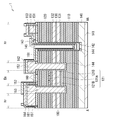
- FIG. 2 is a vertical cross-sectional view showing the configuration of the light emitting element 1 according to the present embodiment.
- FIG. 2 schematically shows a cross-sectional view taken along the line AA of FIG.
- the light emitting element 1 is a surface light emitting type semiconductor laser.
- the light emitting element 1 includes a laminated structure 100 on the first surface side (that is, the surface side) of the substrate 140.
- the first reflector 110, the first spacer layer 131, the active layer 130, the second spacer layer 132, the current constriction layer 121, and the second reflector 120 are laminated in this order from the substrate 140 side. It is provided in.
- the laminated structure 100 a part of the first reflector 110, the first spacer layer 131, the active layer 130, the second spacer layer 132, the current constriction layer 121, and the second reflector 120 are laminated in the lamination direction.
- a separation groove 153 that is dug in an annular shape is provided.
- a separation layer 152 is provided inside the separation groove 153 via a first insulating layer 144.
- the separation groove 153 and the laminated structure 100 of the inner region of the separation layer 152 function as a light emitting portion Em for emitting a laser.
- the substrate 140 is, for example, an n-type GaAs substrate. More specifically, the substrate 140 may be a (100) -plane GaAs substrate or a (n11) -plane GaAs substrate (n is an integer).
- the first reflector 110 is a multilayer film reflector in which a plurality of sets of low refractive index layers and high refractive index layers are alternately laminated.
- the first reflector 110 has an n-type Al x1 Ga 1-x1 having a thickness of ⁇ 0 / n 1 ( ⁇ 0 is the oscillation wavelength of the active layer 130 and n 1 is the refractive index of the low refractive index layer).
- a low refractive index layer composed of As (0 ⁇ x1 ⁇ 1) and a thickness of ⁇ 0 / n 2 ( ⁇ 0 is the oscillation wavelength of the active layer 130, n 2 is the refractive index of the high refractive index layer).
- It may be a multilayer film reflector in which high refractive index layers composed of n-type Al x2 Ga 1-x2 As (0 ⁇ x2 ⁇ x1) are alternately laminated.
- the first spacer layer 131 is composed of, for example, n-type Al x3 Ga 1-x3 As (0 ⁇ x3 ⁇ 1)
- the second spacer layer 132 is, for example, p-type Al x5 Ga 1-x5 As (0 ⁇ 1). It is composed of x5 ⁇ 1).
- the p-type impurity contained in the second spacer layer 132 may be, for example, carbon (C), beryllium (Be), magnesium (Mg), zinc (Zn), or the like.
- the active layer 130 is composed of, for example, undoped Al x4 Ga 1-x4 As (0 ⁇ x4 ⁇ 1), and emits light by injecting an electric current. Specifically, in the active layer 130, the region facing the current injection region 121A of the current constriction layer 121, which will be described later, emits light by injecting the current.
- the second reflector 120 is a multilayer film reflector in which a plurality of sets of low refractive index layers and high refractive index layers are alternately laminated.
- the second reflector 120 has a thickness of ⁇ 0 / n 3 ( ⁇ 0 is the oscillation wavelength of the active layer 130, n 3 is the refractive index of the low refractive index layer) p-type Al x6 Ga 1-x6.
- a low refractive index layer composed of As (0 ⁇ x6 ⁇ 1) and a thickness of ⁇ 0 / n 4 ( ⁇ 0 is the oscillation wavelength of the active layer 130, n 4 is the refractive index of the high refractive index layer).
- It may be a multilayer film reflector in which high refractive index layers composed of p-type Al x7 Ga 1-x7 As (0 ⁇ x7 ⁇ x1) are alternately laminated.
- the p-type impurities contained in the low refractive index layer and the high refractive index layer constituting the second reflector 120 are, for example, carbon (C), beryllium (Be), magnesium (Mg), zinc (Zn) and the like. There may be.
- the current constriction layer 121 is provided inside the second reflector 120 in place of a low refractive index layer several layers away from the active layer 130 side of the second reflector 120.
- the current constriction layer 121 includes a current injection region 121A and a current constriction region 121B in the in-plane direction perpendicular to the stacking direction.
- the current injection region 121A is a region composed of p-type Al x8 Ga 1-x8 As (0 ⁇ x8 ⁇ 1).
- the current constriction region 121B is a region including aluminum oxide (Al 2 O 3 ) and provided in the outer edge region of the current injection region 121A. According to this configuration, the current constriction layer 121 can constrict the region through which the current flows to the current injection region 121A.
- the current constriction region 121B can be formed by oxidizing the high-concentration aluminum (Al) contained in the current constriction layer 121 from the side surface of the separation groove 153 when the separation groove 153 is formed.
- the current constriction region 121B may be provided as an oxidation region in which the current constriction layer 121 made of AlAs (aluminum arsenide) is oxidized from the side surface of the separation groove 153.
- the current injection region 121A may be provided as an unoxidized region of the current constriction layer 121 made of AlAs (aluminum arsenide).
- the separation groove 153 has an annular planar shape, and is a groove for digging the laminated structure 100 into a region deeper than the active layer 130 in the laminating direction.
- the separation groove 153 is provided to electrically or optically separate the light emitting portion Em from other regions.
- the separation groove 153 penetrates the second reflector 120, the current constriction layer 121, the second spacer layer 132, the active layer 130, and the first spacer layer 131, and reaches a part of the first reflector 110. It may be provided by digging up to the laminated structure 100.
- the first insulating layer 144 is provided so as to cover the inside of the separation groove 153 with an insulating material. Specifically, the first insulating layer 144 may be provided so as to cover the inner bottom surface and side surface of the separation layer 152 with silicon nitride (SiN) or the like.
- the separation layer 152 is provided with an organic resin so as to embed the inside of the separation groove 153 via the first insulating layer 144.
- the separation layer 152 may be provided by embedding the inside of the separation groove 153 with benzocyclobutene (BCB), which is a kind of low dielectric constant resin.
- BCB benzocyclobutene
- An annular second electrode 160 is provided on the surface of the laminated structure 100 of the light emitting portion Em on the second reflector 120 side.
- the second electrode 160 is electrically connected to the second electrode pad 164 provided on the laminated structure 100 outside the light emitting portion Em via the first insulating layer 144, the pad base portion 151, and the second insulating layer 161. Connected to.
- the second electrode 160 is provided on the surface of the laminated structure 100 on the second reflector 120 side in an annular shape in which a region facing the current injection region 121A is opened.
- the second electrode 160 may have a shape other than the annular shape as long as it does not cover the region facing the current injection region 121A.
- the second electrode 160 is provided, for example, by laminating an alloy of gold (Au) and germanium (Ge) and an alloy of gold (Au) and nickel (Ni) in order from the side of the second reflector 120. You may.
- the first electrode 141 is provided on the second surface (that is, the back surface) opposite to the first surface on which the laminated structure 100 of the substrate 140 is provided.
- the first electrode 141 has a first insulating layer 144 and a pad base on the laminated structure 100 outside the light emitting portion Em by the first electrode contacts 142 and 143 provided inside the opening 145 penetrating the laminated structure 100. It is electrically connected to the first electrode pad 163 provided via the portion 151 and the second insulating layer 161.
- the first electrode 141 is provided so as to spread over the entire surface of the second surface of the substrate 140.
- the first electrode 141 may be provided, for example, by laminating an alloy of gold (Au) and germanium (Ge) and an alloy of gold (Au) and nickel (Ni) in order from the substrate 140 side.
- the first electrode contacts 142 and 143 are provided inside the opening 145 that is dug through the laminated structure 100 until it reaches the substrate 140, and electrically connects the first electrode 141 and the first electrode pad 163. .. Specifically, the first electrode contact 142 is provided on the bottom surface of the opening 145. The first electrode contact 143 is provided on the bottom surface and the side surface of the opening 145 via the first electrode contact 142 and the first insulating layer 144. The first electrode contacts 142 and 143 are provided by laminating an alloy of gold (Au) and germanium (Ge) and an alloy of gold (Au) and nickel (Ni) in order from the side of the first electrode 141. May be good.
- the pad base portion 151 is provided in the outer region of the light emitting portion Em as an insulating layer continuous with the separation layer 152. Specifically, the pad base portion 151 is provided by laminating an organic resin forming the separation layer 152 on the surface of the laminated structure 100 in the outer region of the light emitting portion Em via the first insulating layer 144. Be done. Similar to the separation layer 152, when the pad base 151 is provided with a low dielectric constant resin such as benzocyclobutene, the light emitting element 1 is located between the second electrode pad 164 and the first electrode pad 163 and the laminated structure 100. Capacity can be reduced.
- the second insulating layer 161 is provided on the surfaces of the pad base portion 151, the separating layer 152, and the laminated structure 100 with an insulating material. Specifically, the second insulating layer 161 excludes the electrical contact between the second electrode 160 and the second electrode pad 164 and the electrical contact between the first electrode contact 143 and the first electrode pad 163. , It may be provided with a uniform thickness along the surface shape of the light emitting element 1.
- the second insulating layer 161 may be provided with an insulating silicon compound such as silicon nitride (SiN).
- the second electrode pad 164 is provided on the pad base portion 151 adjacent to the light emitting portion Em via the second insulating layer 161.
- the second electrode pad 164 is electrically connected to the second electrode 160, and functions as a connection terminal between the second electrode 160 and the outside.
- the second electrode pad 164 can be provided, for example, by laminating titanium (Ti), platinum (Pt), and gold (Au) in this order from the pad base portion 151 side.
- the first electrode pad 163 is provided on the pad base portion 151 in a region different from the pad base portion 151 on which the second electrode pad 164 is provided via the second insulating layer 161.
- the first electrode pad 163 is electrically connected to the first electrode contact 143 and functions as a connection terminal between the first electrode 141 and the outside.
- the first electrode pad 163 can be provided, for example, by laminating titanium (Ti), platinum (Pt), and gold (Au) in this order from the pad base portion 151 side.
- the third insulating layer 162 is provided on the surfaces of the second electrode pad 164, the first electrode pad 163, and the second insulating layer 161 with an insulating material. Specifically, the third insulating layer 162 is uniform along the surface shape of the light emitting element 1 excluding a part of the area above the second electrode pad 164 and a part of the area above the first electrode pad 163. It may be provided with the thickness of.
- the third insulating layer 162 may be provided with an insulating silicon compound such as silicon nitride (SiN).
- the light emitting portion Em and the outer region of the separation layer 152 are provided as the high resistance region Hr.
- the high resistance region Hr is a region in which the electric resistance of the laminated structure 100 is higher than the electric resistance of the laminated structure 100 of the light emitting portion Em.
- the high resistance region Hr is provided by introducing an impurity element into the laminated structure 100 from the second reflector 120 side to a region deeper than the depth at which the active layer 130 is provided.
- the impurities that increase the electrical resistance of the laminated structure 100 by being introduced into the laminated structure 100 include, for example, hydrogen (H), carbon (C), boron (B), oxygen (O), argon (Ar), and aluminum ( It may be any one or more of Al), gallium (Ga), or arsenic (As).
- H hydrogen
- C carbon
- B boron
- O oxygen
- Ar argon
- Al aluminum
- Ga gallium
- Ar arsenic
- one or more of C, B, O, Ar, Al, Ga, or As is laminated in the laminated structure 100, and 5 ⁇ 10 13 pieces / cm 2 or more. It may be formed by introducing at a concentration.
- the high resistance region Hr may be formed by introducing H into the laminated structure 100 at a concentration of 5 ⁇ 10 14 pieces / cm 2 or more by using an ion implantation method.
- the impurity element to be introduced into the laminated structure 100 is H
- the energy for introducing the impurity element into the laminated structure 100 by the ion implantation method becomes small, so that the cost of the step of forming the high resistance region Hr can be reduced. Can be done.
- the laminated structure 100 of the high resistance region Hr has a concentration distribution of impurity elements in the laminated direction.
- the concentration peak of the impurity element may be provided at the depth at which the active layer 130 or the current constriction layer 121 is provided.
- the impurity element is introduced into the laminated structure 100 so that the concentration peak of the impurity element exists at the depth where the active layer 130 or the current constriction layer 121 is provided, the laminated structure 100 is more reliably introduced to the desired depth. Impurity elements are introduced. Therefore, in the light emitting element 1, the laminated structure 100 is more reliably increased in resistance, and the high resistance region Hr is formed.
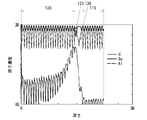
- FIG. 3 shows an example of the concentration distribution of impurity elements in the laminated structure 100 of the high resistance region Hr.
- FIG. 3 is a graph showing an example of the distribution of the element concentration in the stacking direction of the laminated structure 100 of the high resistance region Hr.
- the graph shown in FIG. 3 is an example of the distribution of the element concentrations of H (hydrogen), Ga (gallium), and Al (aluminum) in the stacking direction when H (hydrogen) is introduced into the laminated structure 100 as an impurity element. Shown.
- the graph shown in FIG. 3 shows an example of the result of analyzing the element concentration of the laminated structure 100 by the secondary ion mass spectrometry (SIMS).
- SIMS secondary ion mass spectrometry
- the region where the Ga concentration is significantly reduced corresponds to the current constriction layer 121 (more specifically, the current constriction region 121B), and the region where the Al concentration is widely reduced.
- the active layer 130 corresponds to the active layer 130. Therefore, the shallower region with the active layer 130 as the boundary corresponds to the second reflector 120, and the deeper region with the active layer 130 as the boundary corresponds to the first reflector 110.
- the element concentration of H in the laminated structure 100 is oscillated by the matrix effect of SIMS caused by the difference in Al concentration of each layer of the multilayer film reflector constituting the second reflector 120. However, it gradually increases from the second reflector 120 side toward the depth direction, and peaks near the depth at which the current constriction layer 121 or the active layer 130 is provided.
- H is introduced into the laminated structure 100 with such a concentration distribution, sufficient H is introduced into the laminated structure 100 on the second reflector 120 side, so that the laminated structure 100 is more reliably increased in resistance.
- the parasitic capacitance generated in the second electrode pad 164 and the first electrode pad 163 can be further reduced.
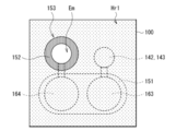
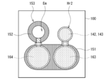
- FIGS. 4 and 5 are top views of the light emitting element 1 showing an example of a region in which the high resistance region Hr is provided.
- the high resistance region Hr1 may be provided in a region excluding the light emitting portion Em and the separation layer 152.
- the light emitting element 1 can further reduce the parasitic capacitance generated in each of the wiring or the electrode.
- the high resistance region Hr2 is provided in the second electrode pad 164, the first electrode pad 163, the first electrode contacts 142 and 143, and the region provided with the wiring for electrically connecting them. It may be provided.
- the light emitting element 1 efficiently reduces the parasitic capacitance generated in each of the wiring or the electrode by introducing a smaller amount of impurity elements. can do.
- a predetermined voltage is applied between the second electrode 160 and the first electrode 141 via the second electrode pad 164 and the first electrode pad 163.
- a current is injected into the active layer 130 through the current injection region 121A of the current constriction layer 121, and light emission is generated by recombination of electrons and holes in the active layer 130.
- the light emitted from the active layer 130 is reflected by the first reflector 110 and the second reflector 120 to generate laser oscillation at a predetermined wavelength, and is emitted from the light emitting unit Em as a laser beam. Will be done. That is, the light emitting element 1 according to the present embodiment functions as a surface emitting type semiconductor laser.
- the light emitting element 1 is used, for example, as a light source for optical communication by an optical fiber. Therefore, in order to improve the communication speed or communication quality of optical communication, the light emitting element 1 is required to improve high frequency characteristics such as modulation speed.
- the laminated structure 100 in the region where the second electrode pad 164, the first electrode pad 163, and the first electrode contacts 142 and 143 are provided outside the separation groove 153 is made highly resistant.
- the parasitic capacitance generated in the second electrode pad 164, the first electrode pad 163, and the like can be reduced. According to this, since the light emitting element 1 can reduce the CR time constant, it is possible to improve high frequency characteristics such as modulation speed.
- the parasitic capacitance generated in the light emitting portion Em is reduced, and the capacitance C of the light emitting element 1 is further reduced. It is also possible to do.
- the resistance of the laminated structure 100 inside the separation groove 153 including the light emitting portion Em is increased, the path through which the current flows in the light emitting portion Em is narrowed, so that the resistance R of the light emitting element 1 is increased. It ends up. Therefore, in such a case, in the light emitting element 1, the decrease in the capacitance C is offset by the increase in the resistance R, so that the CR time constant is rather increased.
- the laminated structure 100 in the outer region of the separation groove 153 surrounding the light emitting portion Em is increased in resistance. According to this, the light emitting element 1 according to the present embodiment can reduce the capacitance C while suppressing an increase in the resistance R of the light emitting element 1.
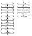
- FIG. 6 is a flowchart illustrating a flow of a manufacturing method of the light emitting element 1 according to the present embodiment.
- 7 to 9 are vertical cross-sectional views illustrating one step of the manufacturing method of the light emitting element 1 according to the present embodiment.
- FIG. 10 is a plan view showing the plan shape of the separation groove 153 and the current constriction region 121B.
- the laminated structure 100 in which the first reflector 110, the first spacer layer 131, the active layer 130, the second spacer layer 132, the current constriction layer 121, and the second reflector 120 are laminated is prepared.
- the substrate 140 is prepared, and alignment is performed to form the separation groove 153 in the laminated structure 100 (S101).
- the substrate 140 is, for example, a GaAs substrate.
- the laminated structure 100 can be formed by sequentially depositing group III-V compound semiconductors by the MOVCD (Metalorganic Chemical Vapor Deposition) method.
- a raw material for the III-V compound semiconductor for example, trimethylaluminum (TMA), trimethylgallium (TMG), trimethylindium (TMIn), arsine (AsH 3 ) and the like are used.
- TMA trimethylaluminum
- TMG trimethylgallium
- TMIn trimethylindium
- AsH 3 arsine
- hydrogen selenide (H 2 Se) or disilane (Si 2 H 6 ) is used as a raw material for n-type impurities
- DMZ dimethylzinc
- carbon tetrabromide is used as a raw material for p-type impurities.
- Carbon tetrabromide (CBr 4 ) is used.
- RIE reactive Ion Etching
- the separation groove 153 is formed as shown in FIG. 7 (S103).
- the separation groove 153 is formed by selectively removing the upper part of the vessel 110.
- the planar shape of the separation groove 153 may be an annular shape, for example, as shown in FIG.
- the current constriction layer 121 is oxidized from the side surface of the separation groove 153 to form the current constriction region 121B and the current injection region 121A (S105).
- Al contained in the current constriction layer 121 is selectively oxidized from the side surface of the separation groove 153.
- a current constriction region 121B containing aluminum oxide (Al 2 O 3 ) is formed around each of the inside and the outside of the separation groove 153, and the inside surrounded by the current constriction region 121B.
- a current injection region 121A is formed in the unoxidized region.
- an impurity element such as hydrogen (H) is laminated in a laminated structure 100 using a resist 150 patterned so as to cover the separation groove 153 and the light emitting portion Em inside the separation groove 153 as a mask. Is ion-implanted in (S107). As a result, the laminated structure 100 in the outer region of the separation groove 153 is increased in resistance, so that the high resistance region Hr is formed.
- an annular second electrode 160 having an opening in a region facing the current injection region 121A is formed in the light emitting portion Em inside the separation groove 153 (109).
- an opening 145 penetrating the laminated structure 100 is formed in a part of the surface of the laminated structure 100 (S111).
- the first insulating layer 144 is formed by forming a film of SiN or the like along the surface of the laminated structure 100, the inside of the separation groove 153, and the inside of the opening 145 (S113).
- the separation layer 152 is formed by embedding the separation groove 153 with a low dielectric constant resin such as benzocyclobutene (BCB) (S117). At this time, a low dielectric constant resin such as benzocyclobutene is also deposited in the outer region of the separation groove 153, so that the pad base portion 151 is formed.
- a low dielectric constant resin such as benzocyclobutene
- the second insulating layer 161 is formed by forming a film of SiN or the like along the surface shapes of the laminated structure 100, the separation layer 152, and the pad base portion 151 (S119). Subsequently, the second electrode pad 164 electrically connected to the second electrode 160 via the opening provided in the second insulating layer 161 on the pad base portion 151, and the first electrode contact 143 and electricity. A first electrode pad 163 to be specifically connected is formed (S121).
- the third insulating layer 162 is formed by forming a film of SiN or the like so as to cover the first electrode pad 163, the second electrode pad 164, and the second insulating layer 161.
- the third insulating layer 162 is provided with an opening in a region corresponding to each of the first electrode pad 163 and the second electrode pad 164.
- the substrate 140 is thinned by appropriately polishing the second surface opposite to the first surface on which the laminated structure 100 of the substrate 140 is provided (S125). After that, the first electrode 141 is formed on the second surface of the substrate 140 (S127), and the first electrode 141 is alloyed (S129). By the above steps, the light emitting element 1 according to the present embodiment is manufactured.
- the annular shape is exemplified as the planar shape of the separation groove 153, but the planar shape of the separation groove 153 in the light emitting element 1 according to the present embodiment is not limited to the above example.
- variations in the planar shape of the separation groove 153 will be described with reference to FIGS. 11A to 11F.
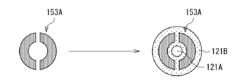
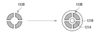
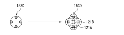
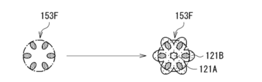
- 11A to 11F are plan views showing variations in the plan shape of the separation groove 153 and the current constriction region 121B.
- the separation groove 153A may be formed by dividing the annular shape into two by one straight line passing through the center of the annular shape. Since the current constriction region 121B is formed so as to spread around the region provided with the separation groove 153A, the current constriction region 121B is formed so as to continuously surround the current injection region 121A even if the separation groove 153A is not continuously provided. It is possible. According to this, the separation groove 153A can electrically or optically separate the light emitting portion Em provided on the inner side from the outer region. In such a case, the high resistance region Hr is provided, for example, in the outer region of the divided annular shape.
- the separation grooves 153B and 153C may be formed by dividing the annular shape into four or six by a plurality of straight lines passing through the center of the annular shape. .. Since the current constriction region 121B is formed so as to extend beyond the divided portion of the separation grooves 153B and 153C, the separation grooves 153B and 153C can also be formed so as to continuously surround the current injection region 121A. .. According to this, the separation grooves 153B and 153C can electrically or optically separate the light emitting portion Em provided on the inner side from the outer region. In such a case, the high resistance region Hr is provided, for example, in the outer region of the divided annular shape.
- the separation grooves 153D, 153E, and 153F may be composed of a plurality of symmetrically provided grooves.
- the separation grooves 153D, 153E, and 153F may be composed of a plurality of circular or elliptical grooves symmetrically arranged along the circumference. Since the current constriction region 121B is formed so as to extend isotropically from the respective grooves of the separation grooves 153D, 153E, and 153F, the respective grooves provided at predetermined intervals are connected to each other to continuously connect the current injection region 121A. It can be formed so as to surround it. In such a case, the high resistance region Hr is provided in the region outside the circle circumscribing each of the separation grooves 153D, 153E, and 153F.
- the separation groove 153 can be formed in various planar shapes if the current constriction region 121B can be continuously provided around the current injection region 121A. Is. At this time, the high resistance region Hr is provided outside the planar circumscribed circle of the separation groove 153, so that the above-mentioned effect can be obtained.
- the technology according to the present disclosure can also have the following configuration.
- the light emitting element can reduce the parasitic capacitance generated in the electrode or the wiring. Therefore, since the light emitting element can reduce the CR time constant, it is possible to improve high frequency characteristics such as modulation speed.
- the effects produced by the techniques according to the present disclosure are not necessarily limited to the effects described herein, and may be any of the effects described in the present disclosure.
- a separation groove provided with symmetry around the light emitting portion on the light emitting surface from the laminated structure in the first direction and digging the laminated structure in the first direction.
- a high resistance region provided in the laminated structure outside the outermost peripheral shape of the separation groove on the injection surface and having a higher electrical resistance than the light injection portion.
- a light emitting element (2) The light emitting element according to (1) above, wherein the high resistance region is provided with an electrode for injecting an electric current into the active layer and a wiring electrically connected to the electrode.
- a current constriction layer that surrounds the unoxidized region with an annular oxidized region in the in-plane direction perpendicular to the first direction is further provided between the injection surface and the active layer.
- the light emitting device according to (14) above, wherein the distribution of the content of the impurity element has a peak at the depth at which the current constriction layer is provided in the first direction.
- the first reflector and the second reflector are each provided by a multilayer film reflector.
- the active layer contains a GaAs-based semiconductor.
Landscapes
- Physics & Mathematics (AREA)
- Condensed Matter Physics & Semiconductors (AREA)
- General Physics & Mathematics (AREA)
- Electromagnetism (AREA)
- Optics & Photonics (AREA)
- Geometry (AREA)
- Semiconductor Lasers (AREA)
Abstract
Description
1.発光素子の構成
2.作用効果
3.発光素子の製造方法
まず、図1及び図2を参照して、本開示の一実施形態に係る発光素子1の構成について説明する。図1は、本実施形態に係る発光素子1の構成を示す上面図であり、図2は、本実施形態に係る発光素子1の構成を示す縦断面図である。図2では、図1のA-AA線で切断した断面図を模式的に示している。
続いて、本実施形態に係る発光素子1の作用効果について説明する。
次に、図6~図10を参照して、本実施形態に係る発光素子1の製造方法について説明する。図6は、本実施形態に係る発光素子1の製造方法の流れを説明するフローチャート図である。図7~図9は、本実施形態に係る発光素子1の製造方法の一工程を説明する縦断面図である。図10は、分離溝153、及び電流狭窄領域121Bの平面形状を示す平面図である。
(1)
電流の注入によって発光する活性層と、前記活性層を挟んで第1方向に積層された第1の反射器、及び第2の反射器とを含む積層構造を有する光射出部と、
前記第1方向における前記積層構造からの光の射出面にて前記光射出部の周囲に対称性を有して設けられ、前記第1方向に前記積層構造を掘り込んだ分離溝と、
前記分離溝の前記射出面における最外周形状よりも外側の前記積層構造に設けられ、前記光射出部よりも電気抵抗が高い高抵抗領域と、
を備える、発光素子。
(2)
前記高抵抗領域には、前記活性層に電流を注入する電極、及び前記電極と電気的に接続する配線が設けられる、上記(1)に記載の発光素子。
(3)
前記射出面と、前記活性層との間には、前記第1方向と垂直な面内方向にて未酸化領域を環状の酸化領域で囲む電流狭窄層がさらに設けられる、上記(1)又は(2)に記載の発光素子。
(4)
前記酸化領域は、前記未酸化領域の周囲を連続して囲む、上記(3)に記載の発光素子。
(5)
前記分離溝の前記射出面からの掘り込み深さは、前記活性層が設けられた深さよりも深い、上記(1)~(4)のいずれか一項に記載の発光素子。
(6)
前記分離溝は、前記光射出部を囲む環形状の溝を含む、上記(1)~(5)のいずれか一項に記載の発光素子。
(7)
前記分離溝は、前記光射出部の周囲に互いに離隔されて対称的に配列された複数の溝を含む、上記(1)~(5)のいずれか一項に記載の発光素子。
(8)
前記高抵抗領域は、前記射出面から前記第1方向に前記活性層が設けられる深さよりも深く広がって設けられる、上記(1)~(7)のいずれか一項に記載の発光素子。
(9)
前記高抵抗領域の前記積層構造は、不純物元素を含む、上記(1)~(8)のいずれか一項に記載の発光素子。
(10)
前記不純物元素は、H、C、B、O、Ar、Al、Ga、又はAsのいずれか1つ以上を含む、上記(9)に記載の発光素子。
(11)
前記不純物元素の含有量は、5×10¹³個/cm2以上である、上記(10)に記載の発光素子。
(12)
前記不純物元素は、Hである、上記(10)又は(11)に記載の発光素子。
(13)
前記不純物元素の含有量は、5×10¹⁴個/cm2以上である、上記(12)に記載の発光素子。
(14)
前記不純物元素の含有量は、前記第1方向に分布を有する、上記(9)~(13)のいずれか一項に記載の発光素子。
(15)
前記不純物元素の含有量の分布は、前記第1方向において、前記活性層が設けられた深さにピークを有する、上記(14)に記載の発光素子。
(16)
前記射出面と、前記活性層との間には、前記射出面の面内方向にて未酸化領域を環状の酸化領域で囲む電流狭窄層がさらに設けられ、
前記不純物元素の含有量の分布は、前記第1方向において、前記電流狭窄層が設けられた深さにピークを有する、上記(14)に記載の発光素子。
(17)
前記第1の反射器、及び前記第2の反射器は、それぞれ多層膜反射鏡にて設けられる、上記(1)~(16)のいずれか一項に記載の発光素子。
(18)
前記活性層は、GaAs系半導体を含む、上記(1)~(17)のいずれか一項に記載の発光素子。
Claims (18)
- 電流の注入によって発光する活性層と、前記活性層を挟んで第1方向に積層された第1の反射器、及び第2の反射器とを含む積層構造を有する光射出部と、
前記第1方向における前記積層構造からの光の射出面にて前記光射出部の周囲に対称性を有して設けられ、前記第1方向に前記積層構造を掘り込んだ分離溝と、
前記分離溝の前記射出面における最外周形状よりも外側の前記積層構造に設けられ、前記光射出部よりも電気抵抗が高い高抵抗領域と
を備える、発光素子。 - 前記高抵抗領域には、前記活性層に電流を注入する電極、及び前記電極と電気的に接続する配線が設けられる、請求項1に記載の発光素子。
- 前記射出面と、前記活性層との間には、前記第1方向と垂直な面内方向にて未酸化領域を環状の酸化領域で囲む電流狭窄層がさらに設けられる、請求項1に記載の発光素子。
- 前記酸化領域は、前記未酸化領域の周囲を連続して囲む、請求項3に記載の発光素子。
- 前記分離溝の前記射出面からの掘り込み深さは、前記活性層が設けられた深さよりも深い、請求項1に記載の発光素子。
- 前記分離溝は、前記光射出部を囲む環形状の溝を含む、請求項1に記載の発光素子。
- 前記分離溝は、前記光射出部の周囲に互いに離隔されて対称的に配列された複数の溝を含む、請求項1に記載の発光素子。
- 前記高抵抗領域は、前記射出面から前記第1方向に前記活性層が設けられる深さよりも深く広がって設けられる、請求項1に記載の発光素子。
- 前記高抵抗領域の前記積層構造は、不純物元素を含む、請求項1に記載の発光素子。
- 前記不純物元素は、H、C、B、O、Ar、Al、Ga、又はAsのいずれか1つ以上を含む、請求項9に記載の発光素子。
- 前記不純物元素の含有量は、5×10¹³個/cm2以上である、請求項10に記載の発光素子。
- 前記不純物元素は、Hである、請求項10に記載の発光素子。
- 前記不純物元素の含有量は、5×10¹⁴個/cm2以上である、請求項12に記載の発光素子。
- 前記不純物元素の含有量は、前記第1方向に分布を有する、請求項9に記載の発光素子。
- 前記不純物元素の含有量の分布は、前記第1方向において、前記活性層が設けられた深さにピークを有する、請求項14に記載の発光素子。
- 前記射出面と、前記活性層との間には、前記射出面の面内方向にて未酸化領域を環状の酸化領域で囲む電流狭窄層がさらに設けられ、
前記不純物元素の含有量の分布は、前記第1方向において、前記電流狭窄層が設けられた深さにピークを有する、請求項14に記載の発光素子。 - 前記第1の反射器、及び前記第2の反射器は、それぞれ多層膜反射鏡にて設けられる、請求項1に記載の発光素子。
- 前記活性層は、GaAs系半導体を含む、請求項1に記載の発光素子。
Priority Applications (2)
| Application Number | Priority Date | Filing Date | Title |
|---|---|---|---|
| US17/755,775 US12451670B2 (en) | 2019-11-15 | 2020-11-06 | Light-emitting device |
| JP2021556071A JP7541994B2 (ja) | 2019-11-15 | 2020-11-06 | 発光素子 |
Applications Claiming Priority (2)
| Application Number | Priority Date | Filing Date | Title |
|---|---|---|---|
| JP2019-207371 | 2019-11-15 | ||
| JP2019207371 | 2019-11-15 |
Publications (1)
| Publication Number | Publication Date |
|---|---|
| WO2021095660A1 true WO2021095660A1 (ja) | 2021-05-20 |
Family
ID=75912879
Family Applications (1)
| Application Number | Title | Priority Date | Filing Date |
|---|---|---|---|
| PCT/JP2020/041560 Ceased WO2021095660A1 (ja) | 2019-11-15 | 2020-11-06 | 発光素子 |
Country Status (3)
| Country | Link |
|---|---|
| US (1) | US12451670B2 (ja) |
| JP (1) | JP7541994B2 (ja) |
| WO (1) | WO2021095660A1 (ja) |
Citations (4)
| Publication number | Priority date | Publication date | Assignee | Title |
|---|---|---|---|---|
| JP2008034637A (ja) * | 2006-07-28 | 2008-02-14 | Fuji Xerox Co Ltd | 面発光型半導体レーザおよびその製造方法 |
| JP2008042053A (ja) * | 2006-08-09 | 2008-02-21 | Sony Corp | 半導体発光素子 |
| JP2010114404A (ja) * | 2008-10-08 | 2010-05-20 | Furukawa Electric Co Ltd:The | 面発光レーザ及びその製造方法 |
| JP2012134473A (ja) * | 2010-11-30 | 2012-07-12 | Sumitomo Chemical Co Ltd | 半導体基板、半導体基板の製造方法および垂直共振器面発光レーザ |
Family Cites Families (5)
| Publication number | Priority date | Publication date | Assignee | Title |
|---|---|---|---|---|
| US5328854A (en) * | 1993-03-31 | 1994-07-12 | At&T Bell Laboratories | Fabrication of electronic devices with an internal window |
| JP4050028B2 (ja) * | 2001-09-28 | 2008-02-20 | 株式会社東芝 | 面発光型半導体発光素子 |
| JP2003309325A (ja) | 2002-04-16 | 2003-10-31 | Sony Corp | 面発光半導体レーザ装置およびその製造方法 |
| US8731012B2 (en) | 2012-01-24 | 2014-05-20 | Fuji Xerox Co., Ltd. | Surface emitting semiconductor laser and its manufacturing method, surface emitting semiconductor laser device, optical transmitter, and information processor |
| JP2021009896A (ja) * | 2019-06-28 | 2021-01-28 | 住友電気工業株式会社 | 面発光レーザ |
-
2020
- 2020-11-06 JP JP2021556071A patent/JP7541994B2/ja active Active
- 2020-11-06 WO PCT/JP2020/041560 patent/WO2021095660A1/ja not_active Ceased
- 2020-11-06 US US17/755,775 patent/US12451670B2/en active Active
Patent Citations (4)
| Publication number | Priority date | Publication date | Assignee | Title |
|---|---|---|---|---|
| JP2008034637A (ja) * | 2006-07-28 | 2008-02-14 | Fuji Xerox Co Ltd | 面発光型半導体レーザおよびその製造方法 |
| JP2008042053A (ja) * | 2006-08-09 | 2008-02-21 | Sony Corp | 半導体発光素子 |
| JP2010114404A (ja) * | 2008-10-08 | 2010-05-20 | Furukawa Electric Co Ltd:The | 面発光レーザ及びその製造方法 |
| JP2012134473A (ja) * | 2010-11-30 | 2012-07-12 | Sumitomo Chemical Co Ltd | 半導体基板、半導体基板の製造方法および垂直共振器面発光レーザ |
Also Published As
| Publication number | Publication date |
|---|---|
| US20220393435A1 (en) | 2022-12-08 |
| JPWO2021095660A1 (ja) | 2021-05-20 |
| US12451670B2 (en) | 2025-10-21 |
| JP7541994B2 (ja) | 2024-08-29 |
Similar Documents
| Publication | Publication Date | Title |
|---|---|---|
| US8040934B2 (en) | Vertical cavity surface emitting laser and method of manufacturing thereof | |
| CN113783105B (zh) | 一种垂直腔面发射激光器及其制备方法 | |
| US8027370B2 (en) | Semiconductor device | |
| CN101950923A (zh) | 激光二极管 | |
| JP2010114214A (ja) | 面発光型半導体レーザ素子、面発光型半導体レーザ素子の製造方法、および光送信装置 | |
| JP2006210429A (ja) | 面発光型半導体レーザ | |
| WO2018096850A1 (ja) | 面発光レーザおよび電子機器 | |
| JPWO2019171869A1 (ja) | 面発光レーザ | |
| WO2019107273A1 (ja) | 面発光半導体レーザ | |
| US20110249696A1 (en) | Laser diode | |
| JP2009259857A (ja) | 面発光レーザ素子および面発光レーザ素子アレイ | |
| JP4224981B2 (ja) | 面発光半導体レーザ素子およびその製造方法 | |
| JP7541994B2 (ja) | 発光素子 | |
| US20030021317A1 (en) | Vertical cavity surface emitting laser having improved light output function | |
| US8514905B2 (en) | Laser diode | |
| CN214506047U (zh) | 高对比度光栅及其垂直腔面发射激光器 | |
| JP5261201B2 (ja) | 面発光レーザ、面発光レーザアレイ及びその製造方法 | |
| JP2015028995A (ja) | 面発光レーザアレイ及びその製造方法 | |
| JP2006190762A (ja) | 半導体レーザ | |
| JP2023007740A (ja) | 面発光レーザおよびその製造方法 | |
| JP7622039B2 (ja) | 面発光レーザ | |
| US20240022040A1 (en) | Surface emitting laser and surface emitting laser array | |
| CN121263936A (zh) | 垂直共振器发光元件 | |
| CN121355694A (zh) | 一种垂直腔面发射激光器及其制备方法 | |
| CN121569410A (zh) | 具有有机保护层的二维vcsel阵列 |
Legal Events
| Date | Code | Title | Description |
|---|---|---|---|
| 121 | Ep: the epo has been informed by wipo that ep was designated in this application |
Ref document number: 20886483 Country of ref document: EP Kind code of ref document: A1 |
|
| ENP | Entry into the national phase |
Ref document number: 2021556071 Country of ref document: JP Kind code of ref document: A |
|
| NENP | Non-entry into the national phase |
Ref country code: DE |
|
| 122 | Ep: pct application non-entry in european phase |
Ref document number: 20886483 Country of ref document: EP Kind code of ref document: A1 |
|
| WWG | Wipo information: grant in national office |
Ref document number: 17755775 Country of ref document: US |