WO2021065725A1 - レーザー素子、化合物、化合物の製造方法、レージング増感剤 - Google Patents
レーザー素子、化合物、化合物の製造方法、レージング増感剤 Download PDFInfo
- Publication number
- WO2021065725A1 WO2021065725A1 PCT/JP2020/036305 JP2020036305W WO2021065725A1 WO 2021065725 A1 WO2021065725 A1 WO 2021065725A1 JP 2020036305 W JP2020036305 W JP 2020036305W WO 2021065725 A1 WO2021065725 A1 WO 2021065725A1
- Authority
- WO
- WIPO (PCT)
- Prior art keywords
- group
- general formula
- substituted
- compound
- compound represented
- Prior art date
- Legal status (The legal status is an assumption and is not a legal conclusion. Google has not performed a legal analysis and makes no representation as to the accuracy of the status listed.)
- Ceased
Links
Images


Classifications
-
- H—ELECTRICITY
- H10—SEMICONDUCTOR DEVICES; ELECTRIC SOLID-STATE DEVICES NOT OTHERWISE PROVIDED FOR
- H10K—ORGANIC ELECTRIC SOLID-STATE DEVICES
- H10K50/00—Organic light-emitting devices
-
- C—CHEMISTRY; METALLURGY
- C07—ORGANIC CHEMISTRY
- C07F—ACYCLIC, CARBOCYCLIC OR HETEROCYCLIC COMPOUNDS CONTAINING ELEMENTS OTHER THAN CARBON, HYDROGEN, HALOGEN, OXYGEN, NITROGEN, SULFUR, SELENIUM OR TELLURIUM
- C07F9/00—Compounds containing elements of Groups 5 or 15 of the Periodic Table
- C07F9/02—Phosphorus compounds
- C07F9/547—Heterocyclic compounds, e.g. containing phosphorus as a ring hetero atom
- C07F9/6564—Heterocyclic compounds, e.g. containing phosphorus as a ring hetero atom having phosphorus atoms, with or without nitrogen, oxygen, sulfur, selenium or tellurium atoms, as ring hetero atoms
- C07F9/6568—Heterocyclic compounds, e.g. containing phosphorus as a ring hetero atom having phosphorus atoms, with or without nitrogen, oxygen, sulfur, selenium or tellurium atoms, as ring hetero atoms having phosphorus atoms as the only ring hetero atoms
- C07F9/65683—Heterocyclic compounds, e.g. containing phosphorus as a ring hetero atom having phosphorus atoms, with or without nitrogen, oxygen, sulfur, selenium or tellurium atoms, as ring hetero atoms having phosphorus atoms as the only ring hetero atoms the ring phosphorus atom being part of a phosphine
-
- C—CHEMISTRY; METALLURGY
- C07—ORGANIC CHEMISTRY
- C07F—ACYCLIC, CARBOCYCLIC OR HETEROCYCLIC COMPOUNDS CONTAINING ELEMENTS OTHER THAN CARBON, HYDROGEN, HALOGEN, OXYGEN, NITROGEN, SULFUR, SELENIUM OR TELLURIUM
- C07F9/00—Compounds containing elements of Groups 5 or 15 of the Periodic Table
- C07F9/02—Phosphorus compounds
- C07F9/547—Heterocyclic compounds, e.g. containing phosphorus as a ring hetero atom
- C07F9/6564—Heterocyclic compounds, e.g. containing phosphorus as a ring hetero atom having phosphorus atoms, with or without nitrogen, oxygen, sulfur, selenium or tellurium atoms, as ring hetero atoms
- C07F9/6568—Heterocyclic compounds, e.g. containing phosphorus as a ring hetero atom having phosphorus atoms, with or without nitrogen, oxygen, sulfur, selenium or tellurium atoms, as ring hetero atoms having phosphorus atoms as the only ring hetero atoms
- C07F9/65686—Heterocyclic compounds, e.g. containing phosphorus as a ring hetero atom having phosphorus atoms, with or without nitrogen, oxygen, sulfur, selenium or tellurium atoms, as ring hetero atoms having phosphorus atoms as the only ring hetero atoms the ring phosphorus atom being part of an organo-phosphorane
-
- C—CHEMISTRY; METALLURGY
- C07—ORGANIC CHEMISTRY
- C07F—ACYCLIC, CARBOCYCLIC OR HETEROCYCLIC COMPOUNDS CONTAINING ELEMENTS OTHER THAN CARBON, HYDROGEN, HALOGEN, OXYGEN, NITROGEN, SULFUR, SELENIUM OR TELLURIUM
- C07F9/00—Compounds containing elements of Groups 5 or 15 of the Periodic Table
- C07F9/02—Phosphorus compounds
- C07F9/547—Heterocyclic compounds, e.g. containing phosphorus as a ring hetero atom
- C07F9/6564—Heterocyclic compounds, e.g. containing phosphorus as a ring hetero atom having phosphorus atoms, with or without nitrogen, oxygen, sulfur, selenium or tellurium atoms, as ring hetero atoms
- C07F9/6581—Heterocyclic compounds, e.g. containing phosphorus as a ring hetero atom having phosphorus atoms, with or without nitrogen, oxygen, sulfur, selenium or tellurium atoms, as ring hetero atoms having phosphorus and nitrogen atoms with or without oxygen or sulfur atoms, as ring hetero atoms
-
- C—CHEMISTRY; METALLURGY
- C09—DYES; PAINTS; POLISHES; NATURAL RESINS; ADHESIVES; COMPOSITIONS NOT OTHERWISE PROVIDED FOR; APPLICATIONS OF MATERIALS NOT OTHERWISE PROVIDED FOR
- C09K—MATERIALS FOR MISCELLANEOUS APPLICATIONS, NOT PROVIDED FOR ELSEWHERE
- C09K11/00—Luminescent materials, e.g. electroluminescent or chemiluminescent
- C09K11/06—Luminescent materials, e.g. electroluminescent or chemiluminescent containing organic luminescent materials
-
- H—ELECTRICITY
- H01—ELECTRIC ELEMENTS
- H01S—DEVICES USING THE PROCESS OF LIGHT AMPLIFICATION BY STIMULATED EMISSION OF RADIATION [LASER] TO AMPLIFY OR GENERATE LIGHT; DEVICES USING STIMULATED EMISSION OF ELECTROMAGNETIC RADIATION IN WAVE RANGES OTHER THAN OPTICAL
- H01S3/00—Lasers, i.e. devices using stimulated emission of electromagnetic radiation in the infrared, visible or ultraviolet wave range
- H01S3/05—Construction or shape of optical resonators; Accommodation of active medium therein; Shape of active medium
- H01S3/06—Construction or shape of active medium
- H01S3/063—Waveguide lasers, i.e. whereby the dimensions of the waveguide are of the order of the light wavelength
- H01S3/0632—Thin film lasers in which light propagates in the plane of the thin film
- H01S3/0635—Thin film lasers in which light propagates in the plane of the thin film provided with a periodic structure, e.g. using distributed feed-back, grating couplers
-
- H—ELECTRICITY
- H01—ELECTRIC ELEMENTS
- H01S—DEVICES USING THE PROCESS OF LIGHT AMPLIFICATION BY STIMULATED EMISSION OF RADIATION [LASER] TO AMPLIFY OR GENERATE LIGHT; DEVICES USING STIMULATED EMISSION OF ELECTROMAGNETIC RADIATION IN WAVE RANGES OTHER THAN OPTICAL
- H01S3/00—Lasers, i.e. devices using stimulated emission of electromagnetic radiation in the infrared, visible or ultraviolet wave range
- H01S3/14—Lasers, i.e. devices using stimulated emission of electromagnetic radiation in the infrared, visible or ultraviolet wave range characterised by the material used as the active medium
- H01S3/16—Solid materials
- H01S3/168—Solid materials using an organic dye dispersed in a solid matrix
-
- H—ELECTRICITY
- H01—ELECTRIC ELEMENTS
- H01S—DEVICES USING THE PROCESS OF LIGHT AMPLIFICATION BY STIMULATED EMISSION OF RADIATION [LASER] TO AMPLIFY OR GENERATE LIGHT; DEVICES USING STIMULATED EMISSION OF ELECTROMAGNETIC RADIATION IN WAVE RANGES OTHER THAN OPTICAL
- H01S5/00—Semiconductor lasers
- H01S5/10—Construction or shape of the optical resonator, e.g. extended or external cavity, coupled cavities, bent-guide, varying width, thickness or composition of the active region
- H01S5/12—Construction or shape of the optical resonator, e.g. extended or external cavity, coupled cavities, bent-guide, varying width, thickness or composition of the active region the resonator having a periodic structure, e.g. in distributed feedback [DFB] lasers
- H01S5/1206—Construction or shape of the optical resonator, e.g. extended or external cavity, coupled cavities, bent-guide, varying width, thickness or composition of the active region the resonator having a periodic structure, e.g. in distributed feedback [DFB] lasers having a non constant or multiplicity of periods
- H01S5/1215—Multiplicity of periods
-
- H—ELECTRICITY
- H01—ELECTRIC ELEMENTS
- H01S—DEVICES USING THE PROCESS OF LIGHT AMPLIFICATION BY STIMULATED EMISSION OF RADIATION [LASER] TO AMPLIFY OR GENERATE LIGHT; DEVICES USING STIMULATED EMISSION OF ELECTROMAGNETIC RADIATION IN WAVE RANGES OTHER THAN OPTICAL
- H01S5/00—Semiconductor lasers
- H01S5/30—Structure or shape of the active region; Materials used for the active region
- H01S5/36—Structure or shape of the active region; Materials used for the active region comprising organic materials
-
- H—ELECTRICITY
- H10—SEMICONDUCTOR DEVICES; ELECTRIC SOLID-STATE DEVICES NOT OTHERWISE PROVIDED FOR
- H10K—ORGANIC ELECTRIC SOLID-STATE DEVICES
- H10K85/00—Organic materials used in the body or electrodes of devices covered by this subclass
- H10K85/60—Organic compounds having low molecular weight
- H10K85/615—Polycyclic condensed aromatic hydrocarbons, e.g. anthracene
- H10K85/622—Polycyclic condensed aromatic hydrocarbons, e.g. anthracene containing four rings, e.g. pyrene
-
- H—ELECTRICITY
- H10—SEMICONDUCTOR DEVICES; ELECTRIC SOLID-STATE DEVICES NOT OTHERWISE PROVIDED FOR
- H10K—ORGANIC ELECTRIC SOLID-STATE DEVICES
- H10K85/00—Organic materials used in the body or electrodes of devices covered by this subclass
- H10K85/60—Organic compounds having low molecular weight
- H10K85/615—Polycyclic condensed aromatic hydrocarbons, e.g. anthracene
- H10K85/624—Polycyclic condensed aromatic hydrocarbons, e.g. anthracene containing six or more rings
-
- H—ELECTRICITY
- H10—SEMICONDUCTOR DEVICES; ELECTRIC SOLID-STATE DEVICES NOT OTHERWISE PROVIDED FOR
- H10K—ORGANIC ELECTRIC SOLID-STATE DEVICES
- H10K85/00—Organic materials used in the body or electrodes of devices covered by this subclass
- H10K85/60—Organic compounds having low molecular weight
- H10K85/649—Aromatic compounds comprising a hetero atom
- H10K85/657—Polycyclic condensed heteroaromatic hydrocarbons
- H10K85/6572—Polycyclic condensed heteroaromatic hydrocarbons comprising only nitrogen in the heteroaromatic polycondensed ring system, e.g. phenanthroline or carbazole
-
- H—ELECTRICITY
- H10—SEMICONDUCTOR DEVICES; ELECTRIC SOLID-STATE DEVICES NOT OTHERWISE PROVIDED FOR
- H10K—ORGANIC ELECTRIC SOLID-STATE DEVICES
- H10K85/00—Organic materials used in the body or electrodes of devices covered by this subclass
- H10K85/60—Organic compounds having low molecular weight
- H10K85/649—Aromatic compounds comprising a hetero atom
- H10K85/657—Polycyclic condensed heteroaromatic hydrocarbons
- H10K85/6574—Polycyclic condensed heteroaromatic hydrocarbons comprising only oxygen in the heteroaromatic polycondensed ring system, e.g. cumarine dyes
-
- C—CHEMISTRY; METALLURGY
- C09—DYES; PAINTS; POLISHES; NATURAL RESINS; ADHESIVES; COMPOSITIONS NOT OTHERWISE PROVIDED FOR; APPLICATIONS OF MATERIALS NOT OTHERWISE PROVIDED FOR
- C09K—MATERIALS FOR MISCELLANEOUS APPLICATIONS, NOT PROVIDED FOR ELSEWHERE
- C09K2211/00—Chemical nature of organic luminescent or tenebrescent compounds
- C09K2211/10—Non-macromolecular compounds
- C09K2211/1003—Carbocyclic compounds
- C09K2211/1007—Non-condensed systems
-
- C—CHEMISTRY; METALLURGY
- C09—DYES; PAINTS; POLISHES; NATURAL RESINS; ADHESIVES; COMPOSITIONS NOT OTHERWISE PROVIDED FOR; APPLICATIONS OF MATERIALS NOT OTHERWISE PROVIDED FOR
- C09K—MATERIALS FOR MISCELLANEOUS APPLICATIONS, NOT PROVIDED FOR ELSEWHERE
- C09K2211/00—Chemical nature of organic luminescent or tenebrescent compounds
- C09K2211/10—Non-macromolecular compounds
- C09K2211/1018—Heterocyclic compounds
- C09K2211/1025—Heterocyclic compounds characterised by ligands
- C09K2211/1096—Heterocyclic compounds characterised by ligands containing other heteroatoms
-
- H—ELECTRICITY
- H01—ELECTRIC ELEMENTS
- H01S—DEVICES USING THE PROCESS OF LIGHT AMPLIFICATION BY STIMULATED EMISSION OF RADIATION [LASER] TO AMPLIFY OR GENERATE LIGHT; DEVICES USING STIMULATED EMISSION OF ELECTROMAGNETIC RADIATION IN WAVE RANGES OTHER THAN OPTICAL
- H01S2301/00—Functional characteristics
- H01S2301/04—Gain spectral shaping, flattening
-
- H—ELECTRICITY
- H01—ELECTRIC ELEMENTS
- H01S—DEVICES USING THE PROCESS OF LIGHT AMPLIFICATION BY STIMULATED EMISSION OF RADIATION [LASER] TO AMPLIFY OR GENERATE LIGHT; DEVICES USING STIMULATED EMISSION OF ELECTROMAGNETIC RADIATION IN WAVE RANGES OTHER THAN OPTICAL
- H01S3/00—Lasers, i.e. devices using stimulated emission of electromagnetic radiation in the infrared, visible or ultraviolet wave range
- H01S3/09—Processes or apparatus for excitation, e.g. pumping
- H01S3/091—Processes or apparatus for excitation, e.g. pumping using optical pumping
- H01S3/094—Processes or apparatus for excitation, e.g. pumping using optical pumping by coherent light
- H01S3/094076—Pulsed or modulated pumping
-
- H—ELECTRICITY
- H01—ELECTRIC ELEMENTS
- H01S—DEVICES USING THE PROCESS OF LIGHT AMPLIFICATION BY STIMULATED EMISSION OF RADIATION [LASER] TO AMPLIFY OR GENERATE LIGHT; DEVICES USING STIMULATED EMISSION OF ELECTROMAGNETIC RADIATION IN WAVE RANGES OTHER THAN OPTICAL
- H01S3/00—Lasers, i.e. devices using stimulated emission of electromagnetic radiation in the infrared, visible or ultraviolet wave range
- H01S3/14—Lasers, i.e. devices using stimulated emission of electromagnetic radiation in the infrared, visible or ultraviolet wave range characterised by the material used as the active medium
- H01S3/16—Solid materials
- H01S3/17—Solid materials amorphous, e.g. glass
- H01S3/176—Solid materials amorphous, e.g. glass silica or silicate glass
-
- H—ELECTRICITY
- H01—ELECTRIC ELEMENTS
- H01S—DEVICES USING THE PROCESS OF LIGHT AMPLIFICATION BY STIMULATED EMISSION OF RADIATION [LASER] TO AMPLIFY OR GENERATE LIGHT; DEVICES USING STIMULATED EMISSION OF ELECTROMAGNETIC RADIATION IN WAVE RANGES OTHER THAN OPTICAL
- H01S5/00—Semiconductor lasers
- H01S5/04—Processes or apparatus for excitation, e.g. pumping, e.g. by electron beams
- H01S5/042—Electrical excitation ; Circuits therefor
- H01S5/0425—Electrodes, e.g. characterised by the structure
- H01S5/04252—Electrodes, e.g. characterised by the structure characterised by the material
- H01S5/04253—Electrodes, e.g. characterised by the structure characterised by the material having specific optical properties, e.g. transparent electrodes
Definitions
- the present invention relates to a compound and a lasing sensitizer useful as a material for a light emitting layer of a laser element.
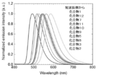
- Non-Patent Document 1 reports that the bisstilbene derivative (BSBCz) represented by the following formula shows an extremely low ASE threshold value and is excellent as an organic laser dye.
- the usefulness of a compound having a stilbene structure as a laser oscillation material is being investigated.
- the realized emission wavelength and laser oscillation characteristics are limited only by the compound having a stilbene structure, and the application range of the organic laser element is limited. Therefore, in order to improve the versatility of the organic laser element, the development of a new laser oscillation material is required.
- the above BSBCz has a characteristic electronic state such as having electron-donating carbazolyl groups at both ends of a long ⁇ -conjugated system, and is expected to have useful applications other than laser oscillation materials. Was done.
- the present inventors have made diligent studies with the aim of providing a new laser oscillation material. Furthermore, the present inventors have made diligent studies for the purpose of developing new uses for BSBCz and its analogs.
- a phosphinin derivative having a specific structure is useful as a laser oscillation material. It was also found that BSBCz and its analogs effectively function as a lasing sensitizer that promotes the light emitting process of the laser oscillator material.
- the present invention has been proposed based on these findings, and specifically has the following configurations.
- a laser device containing a compound represented by the following general formula (1) in a light emitting layer [In the general formula (1), R 1 and R 5 each independently represent a substituent having a positive Hammett ⁇ p value, and R 2 to R 4 and R 6 to R 15 each independently represent a hydrogen atom or a substituent. Represent. ] [2] R 1 and R 5 are independently substituted with a cyano group, an aryl group substituted with a cyano group, or a heteroaryl group having a nitrogen atom as a ring skeleton constituent atom (the aryl group is further substituted with a group other than the cyano group).
- L represents a conjugated linking group containing both a substituted or unsubstituted arylene group and a substituted or unsubstituted ethenylene group.
- the luminescence-excited singlet energy level of the compound represented by the general formula (1) is lower than the luminescence-excited singlet energy level of the compound represented by the general formula (2), and the general The luminescence-excited triplet energy level of the compound represented by the formula (1) is higher than the luminescence-excited triplet energy level of the compound represented by the general formula (2), according to [11] or [12].
- a compound represented by the following general formula (3) [In the general formula (3), R 21 and R 25 each independently represent a substituent having a positive Hammett ⁇ p value, R 23 represents a substituent, and R 22 , R 24 , and R 26 to R 35 , respectively. Represents a hydrogen atom or substituent independently.
- R 23 is a substituted aryl group or a substituted or unsubstituted heteroaryl group.
- R 23 is a substituted aryl group or a substituted or unsubstituted heteroaryl group.
- R 23 is a substituted aryl group.
- R 21 and R 25 are cyano groups.
- 4-position and step of other positions unsubstituted is halogenated at the 4-position of which may be optionally 2,6-dicyano-1,1-diphenyl phosphinyl down substituted, thereafter the R 43 -H
- a method for producing a compound represented by the general formula (4) which comprises a step of reacting the represented compound.
- R 43 represents a substituted aryl group or a substituted or unsubstituted heteroaryl group
- R 42 , R 44 , and R 46 to R 55 each independently represent a hydrogen atom or a substituent.
- the compound of the present invention is useful as a laser oscillation material, which makes it possible to provide a new laser oscillation material having a skeleton structure different from that of BSBCz. Further, the laser element of the present invention can realize excellent laser oscillation characteristics. By using the laser sensitizer of the present invention, the oscillation characteristics of the laser element can be improved.
- the description of the constituent elements described below may be based on typical embodiments and specific examples of the present invention, but the present invention is not limited to such embodiments and specific examples.
- the numerical range represented by using "-" in the present specification means a range including the numerical values before and after "-" as the lower limit value and the upper limit value.
- the isotope species of hydrogen atoms existing in the molecule of the compound used in the present invention is not particularly limited, and for example, all hydrogen atoms in the molecule may be 1 H, or some or all may be 2 H. (Duterium D) may be used.
- the laser element (first laser element) of the present invention contains a compound represented by the following general formula (1) in the light emitting layer.
- the laser device of the present invention exhibits excellent laser oscillation characteristics by containing the compound represented by the general formula (1) in the light emitting layer. This is because the compound represented by the general formula (1) easily forms a population inversion of the excited singlet state, and the intersystem crossing from the excited singlet state to the excited triplet state by irradiation with naturally emitted light or external light. It is presumed that this is because radiation deactivation occurs from the luminescence-excited singlet state at a speed higher than the crossing speed.
- the light emitting layer may be composed of only the compound represented by the general formula (1), or may contain other materials. Hereinafter, the compound represented by the general formula (1) and other light emitting layer materials will be described.
- R 1 and R 5 each independently represent a substituent having a positive Hammett ⁇ p value.
- R 1 and R 5 may be the same or different from each other, but are preferably the same. Since R 1 and R 5 are substituents having a positive Hammett ⁇ p value, respectively, the phosphinin structure tends to be stabilized.
- the “hammet ⁇ p value” is defined by L. P. Proposed by Hammett, it quantifies the effect of substituents on the reaction rate or equilibrium of para-substituted benzene derivatives.
- R 1 and R 5 are preferably cyano groups, aryl groups substituted with cyano groups, or heteroaryl groups having a nitrogen atom as a ring skeleton constituent atom, respectively.
- the aryl group substituted with a cyano group may be further substituted with a group other than the cyano group, and the heteroaryl group having a nitrogen atom as a ring skeleton constituent atom may be substituted.
- the aromatic ring constituting the aryl group may be a monocyclic ring or a condensed ring in which two or more aromatic rings are condensed, or two or more aromatic rings are linked. It may be a connecting ring.
- the aromatic ring constituting the aryl group preferably has 6 to 22 carbon atoms, more preferably 6 to 18 carbon atoms, further preferably 6 to 14 carbon atoms, and even more preferably 6 to 10 carbon atoms. preferable.
- Specific examples of each aryl group include a phenyl group, a naphthyl group, and a biphenyl group.
- the number of substitutions and the substitution position of the cyano group in the aryl group are not particularly limited. A part of the substitutable positions of the aryl group may be substituted with a cyano group, or all the substitutable positions of the aryl group may be substituted with a cyano group.
- the "substituent position” means the position of a hydrogen atom that can be replaced with a substituent.
- the hydrogen atom that can be replaced with the substituent include the hydrogen atom of the methine group constituting the aryl group.
- the remaining substitutable positions may be substituted with a substituent other than the cyano group or may be unsubstituted. ..
- the heteroaryl group constituting the heteroaryl group may be a monocyclic ring, or a fused ring in which two or more heteroaromatic rings having a nitrogen atom are condensed. Alternatively, it may be a fused ring in which at least one of the heteroaromatic rings having a nitrogen atom and at least one of the aromatic rings are condensed.
- the heteroaromatic ring constituting the heteroaryl group preferably contains a 6-membered ring having a nitrogen atom as a ring skeleton constituent atom, and the number of nitrogen atoms in the 6-membered ring is preferably 1 to 3.
- the 6-membered ring having a nitrogen atom as a ring-skeleton constituent atom include a pyridine ring, a pyrazine ring, a pyrimidine ring, a pyridazine ring, and a triazine ring.
- the heteroaryl group having a nitrogen atom as a ring skeleton constituent atom may be substituted with a substituent.
- a substituent which may be further substituted with an aryl group substituted with a cyano group and a substituent which may be substituted with a heteroaryl group having a nitrogen atom as a ring skeleton constituent atom for example, an alkyl having 1 to 20 carbon atoms.
- Examples thereof include a group, an aryl group having 6 to 40 carbon atoms, a cyano group, a halogen atom, and a heteroaryl group having 5 to 40 carbon atoms. Of these substituents, those substitutable by the substituent may be substituted.
- R 2 to R 4 and R 6 to R 15 each independently represent a hydrogen atom or a substituent.
- R 2 ⁇ R 4, R 6 ⁇ R 15 may being the same or different.
- R 2 to R 4 are independent substituents having a positive ⁇ p value of a hydrogen atom or Hammett, and preferably each independently having a negative ⁇ p value of a hydrogen atom or Hammett.
- Each independently is preferably a hydrogen atom, a substituted or unsubstituted aryl group, or a group represented by R 16 CO-.
- R 16 in R 16 CO- is a hydrogen atom or a substituent.
- ⁇ p value is positive substituent Hammett in R 2 ⁇ R 4
- the preferred ranges and examples of the substituents represented by R 2 ⁇ R 4 are, "Hammett's ⁇ p values of R 1 and R 5
- the description of "is a positive substituent” and the preferred range and specific examples of the substituents represented by R 1 and R 5 can be referred to.
- a more preferred substituent is an aryl group substituted with a cyano group.
- Preferable examples of the " ⁇ p value is negative substituent Hammett" in R 2 ⁇ R 4 may be a group containing a diarylamino structure of substituted or unsubstituted.
- the "diarylamino structure” means both a diarylamino group and a heteroaromatic ring structure in which the aryl groups of the diarylamino group are linked by a single bond or a linking group to form a heterocycle.
- the description and preferable range of the aromatic ring constituting each aryl group of the diarylamino structure and specific examples the description of the aromatic ring constituting the aryl group and the preferable range and specific example can be referred to.
- the diarylamino structure may be linked to the phosphinine ring in the general formula (1) with a carbon atom of each aryl group, or may be linked with a nitrogen atom to which each aryl group is bonded. Further, the carbon atom or the nitrogen atom may be bonded to the carbon atom constituting the phosphinin ring by a single bond or may be linked by a linking group. That is, the group containing the diarylamino structure may contain a linking group that links the diarylamino structure to the phosphinine ring.
- the linking group that links the diarylamino structure to the benzene ring is not particularly limited, but is preferably a substituted or unsubstituted arylene group.
- the group containing a diarylamino structure is preferably a group represented by the following general formula (5) or the following general formula (6).
- R 61 to R 70 and R 165 to R 173 each independently represent a hydrogen atom or a substituent.
- One of R 161 to R 164 represents a bond position to the phosphine ring in the general formula (1), and the rest of R 161 to R 164 independently represent a hydrogen atom or a substituent.
- the number of substituents is not particularly limited, and all of R 61 to R 70 and R 161 to R 173 (excluding the bond position to the phosphinin ring) may be unsubstituted (that is, a hydrogen atom).
- the plurality of substituents may be the same or different from each other.
- R 161 to R 173 when two or more of R 161 to R 173 are substituents, the plurality of substituents may be the same or different from each other.
- Possible substituents of R 61 to R 70 and R 161 to R 173 include, for example, a hydroxy group, a halogen atom, an alkyl group having 1 to 20 carbon atoms, an alkoxy group having 1 to 20 carbon atoms, and an alkylthio having 1 to 20 carbon atoms.
- alkyl-substituted amino group with 1 to 20 carbon atoms alkyl-substituted amino group with 1 to 20 carbon atoms, aryl-substituted amino group with 1 to 20 carbon atoms, aryl group with 6 to 40 carbon atoms, heteroaryl group with 3 to 40 carbon atoms, alkenyl with 2 to 10 carbon atoms
- Examples thereof include a group, an alkynyl group having 2 to 10 carbon atoms, an alkylamide group having 2 to 20 carbon atoms, an arylamide group having 7 to 21 carbon atoms, and a trialkylsilyl group having 3 to 20 carbon atoms.
- those substitutable by a substituent may be further substituted.
- More preferable substituents are an alkyl group having 1 to 20 carbon atoms, an alkoxy group having 1 to 20 carbon atoms, an alkylthio group having 1 to 20 carbon atoms, an alkyl substituted amino group having 1 to 20 carbon atoms, and 1 to 20 carbon atoms. It is an aryl-substituted amino group, an aryl group having 6 to 40 carbon atoms, and a heteroaryl group having 3 to 40 carbon atoms.
- R 61 and R 62 , R 62 and R 63 , R 63 and R 64 , R 64 and R 65 , R 65 and R 66 , R 66 and R 67 , R 67 and R 68 , R 68 and R 69 , R 69 And R 70 , R 161 and R 162 , R 162 and R 163 , R 163 and R 164 , R 165 and R 166 , R 166 and R 167 , R 167 and R 168 , R 169 and R 170 , R 170 and R. 171 R 171 and R 172 , and R 172 and R 173 may be coupled to each other to form an annular structure.
- the cyclic structure may be an aromatic ring or an alicyclic ring, may contain a hetero atom, and the cyclic structure may be a fused ring having two or more rings.
- the hetero atom referred to here is preferably one selected from the group consisting of a nitrogen atom, an oxygen atom and a sulfur atom.
- Examples of the cyclic structure formed include a benzene ring, a naphthalene ring, a pyridine ring, a pyridazine ring, a pyrimidine ring, a pyrazine ring, a pyrrol ring, an imidazole ring, a pyrazole ring, an imidazoline ring, an oxazole ring, an isooxazole ring, a thiazole ring, and an iso.
- Examples thereof include a thiazole ring, a cyclohexadiene ring, a cyclohexene ring, a cyclopentaene ring, a cycloheptatriene ring, a cycloheptadiene ring, and a cycloheptaene ring.
- R 65 and R 66 are not connected to each other, those in which R 65 and R 66 are connected to each other to form a single bond, or R 65.
- R 66 are bonded to each other to form a linking group having a chain length of 1 atom, R 65 and R 66 are not linked to each other, and R 65 and R 66 are connected to each other to form a single bond. Those forming a bond are more preferable.
- R 65 and R 66 are bonded to each other to form a linking group having a chain length of 1 atom, the cyclic structure formed as a result of the bonding of R 65 and R 66 to each other is a 6-membered ring.
- linking group formed by bonding R 65 and R 66 to each other are represented by -O-, -S-, -N (R 191 )-or -C (R 192 ) (R 193 )-.
- Linking groups can be mentioned.
- R 191 to R 193 independently represent a hydrogen atom or a substituent.
- substituent that R 191 can take include an alkyl group having 1 to 20 carbon atoms, an aryl group having 6 to 40 carbon atoms, and a heteroaryl group having 3 to 40 carbon atoms.
- R 192 and R 193 include a hydroxy group, a halogen atom, an alkyl group having 1 to 20 carbon atoms, an alkoxy group having 1 to 20 carbon atoms, and an alkylthio group having 1 to 20 carbon atoms, respectively.
- L 61 represents a single-bonded or substituted or unsubstituted arylene group.
- the description and preferable range of the aromatic ring constituting the arylene group and specific examples the description of the aromatic ring constituting the aryl group and the preferable range and specific examples can be referred to.
- Specific examples of the substituted or unsubstituted arylene group in L 61 include a substituted or unsubstituted phenylene group, a substituted or unsubstituted naphthylene group, and a biphenyl-diyl group, which are substituted or unsubstituted phenylene groups. Is preferable.
- the phenylene group may be any of 1,2-phenylene group, 1,3-phenylene group and 1,4-phenylene group, but 1,4-phenylene group is preferable.
- 1,4-phenylene group is preferable.
- the above description of the substituent and the preferable range of R 61 to R 70 and the like can be referred to. * Indicates the bonding position.
- R 91 to R 94 , R 97 to R 108 , R 111 to R 118 , R 121 to R 128 , R 131 to R 135 , and R 141 to R 150 are independent of each other.
- R 104 R 105 and R 106 , R 106 and R 107 , R 107 and R 108 , R 111 and R 112 , R 112 and R 113 , R 113 and R 114 , R 115 and R 116 , R 116 and R.
- R 146 , R 146 and R 147 , R 147 and R 148 , and R 149 and R 150 may be coupled to each other to form an annular structure.
- L 91 , L 101 , L 111 , L 121 , and L 141 each independently represent a single bond or a substituted or unsubstituted arylene group. * Indicates the bonding position.
- the description of the substituent, the cyclic structure and the substituted or unsubstituted arylene group referred to here, and the preferable range and specific examples include the description of the substituent, the cyclic structure and the substituted or unsubstituted arylene group in the general formula (5). Preferred ranges and specific examples can be referred to.
- the aromatic ring constituting the substituted or unsubstituted aryl group in R 2 to R 4 may be a monocyclic ring, or a fused ring in which two or more aromatic rings are condensed, or an aromatic ring. It may be a fused ring in which at least one and at least one of cycloalkene are condensed, a spiro ring in which two or more aromatic rings are bonded to a spiro atom, or a linked ring in which two or more aromatic rings are linked. When two or more aromatic rings are connected, they may be linearly connected or branched.
- the aromatic ring constituting the aryl group is preferably a condensed ring containing a benzene ring unit.
- the aromatic ring constituting the aryl group preferably has 6 to 25 carbon atoms.
- Specific examples of the aryl group include a phenyl group, a naphthyl group, a biphenyl group, a triphenylenyl group, a fluorenyl group, and a 9,9'-spirobifluorenyl group.
- the above description of the substituent and the preferable range of R 61 to R 70 and the like can be referred to.
- R 16 group in R 2 ⁇ R 4 is represented by R 16 CO- may be a substituent be a hydrogen atom.
- substituents include a substituted or unsubstituted alkyl group, a substituted or unsubstituted aryl group, a halogen atom, a cyano group and the like.
- the number of substituents among R 2 to R 4 is not particularly limited, and it is preferable that all of them are unsubstituted, and it is also preferable that at least one of R 2 to R 4 is a substituent.
- the substituent at least R 3 of R 2 to R 4 is preferably a substituent, the substituent is preferably a substituent containing an unsaturated bond, and a substituent containing an aromatic ring. Is more preferable.
- R 6 to R 15 may be hydrogen atoms or substituents.
- the number of substituents among R 6 to R 15 is not particularly limited, and all of them may be unsubstituted.
- R 6 to R 15 the explanation of the substituents that can be taken by R 61 to R 70 and the like and the preferable range can be referred to.
- the compound represented by the general formula (1) is preferably a compound represented by the following general formula (1a).
- R 1a to R 5a are each independently selected from a hydrogen atom or the following substituent group a, and at least one of R 1a to R 5a is selected from the following substituent group a. Substituent. Substituent group a
- Ph represents a phenyl group and Cz represents a carbazolyl group. * Represents the bond position to the benzene ring in the general formula (1a).
- R 1a to R 5a is a group selected from the substituent group a, and the rest of R 1a to R 5a is a hydrogen atom.
- the compound represented by the general formula (1a) is preferably a compound represented by the following formula.
- the light emitting layer may be composed of only the compound represented by the general formula (1), or may contain other components. Examples of other components include compounds represented by the following general formula (2).
- the compound represented by the general formula (2) can obtain the energy obtained by light absorption by the general formula. It effectively functions as a lasing sensitizer to be passed to the compound represented by (1), and can improve the laser oscillation characteristics of the laser element. Therefore, the compound represented by the general formula (2) is useful as a lasing sensitizer.
- Z 1 and Z 2 each independently represent a substituted or unsubstituted diarylamino group, and the two aryl groups constituting the diarylamino group are bonded to each other directly or via a linking group.
- L represents a conjugated linking group containing both a substituted or unsubstituted arylene group and a substituted or unsubstituted ethenylene group.
- L in the general formula (2) is a linking group in which the linking chain connecting Z 1 and Z 2 has a conjugated structure and contains both a substituted or unsubstituted arylene group and a substituted or unsubstituted ethenylene group.
- the description of the aromatic ring constituting the substituted or unsubstituted arylene group in the conjugated system linking group can be referred to. ..
- the arylene group include those having a structure in which two or more phenylene groups such as a phenylene group, a biphenyl-diyl group and a terphenyl-diyl group are linked, and the phenylene group and the biphenyl-diyl group can be mentioned. It is preferable that at least one of them is contained in the conjugated linking group. Further, a fused ring in which an aromatic ring such as a benzene ring is condensed with these arylene groups may be contained in the conjugated linking group.
- the number of benzene rings in L is preferably 1 or more, for example, 2 or more, 3 or more, 4 or more, and 30 or less, 20 or less, 10 or less. ..
- the conjugated linking group has a condensed ring containing a benzene ring unit
- the number of the benzene ring unit is counted.
- a naphthalene ring is counted as two rings
- an anthracene ring is counted as three rings.
- the number of ethenylene groups in L is preferably 1 or more, for example, 2 or more, 3 or more, 4 or more, and 30 or less, 20 or less, 10 or less.
- the conjugated linking group preferably has a structure in which a phenylene group or a biphenyl-diyl group and an ethenylene group are alternately located, and among them, phenylene is directly bonded to Z 1 and Z 2 (bonded by a single bond). It is preferably a group.
- the conjugated linking group may contain a divalent linking group having a heteroaromatic ring together with a substituted or unsubstituted arylene group and a substituted or unsubstituted ethenylene group.
- the heteroaromatic ring referred to here is preferably a 5-membered ring or a 6-membered ring, and examples of the ring-skeleton-constituting heteroatom include a nitrogen atom, an oxygen atom, and a sulfur atom.
- More preferable heteroaromatic rings are a 6-membered ring containing a nitrogen atom as a ring-skeleton-constituting heteroatom and a 5-membered ring containing an oxygen atom as a ring-skeleton-constituting heteroatom. You can raise the ring.
- the conjugated linking group represented by L is, for example, a structure in which two or more benzofuran structures are linked, a structure in which one or more benzofuran structures are linked to one or more benzene rings, or one or more benzofuran structures and one or more. It may have a structure in which one or more benzofuran structures and one or more benzene rings and one or more ethenylene groups are linked.
- the benzene ring and the furan ring constituting the conjugated linking group represented by L may be condensed, and the heteroaromatic ring and the furan ring may also be condensed.
- the conjugated linking group represented by L may have, for example, a structure in which one or more groups selected from the following group A are linked.
- At least one of the ring skeleton constituent atoms of the benzene ring constituting these groups may be substituted with a nitrogen atom.
- the number of nitrogen atoms substituted in one ring is preferably 1 or 2, and in the case of 2, it is preferable that the two nitrogen atoms are substituted at positions where they are not directly bonded (non-adjacent positions).
- the conjugated linking group may have a benzene ring and a furan ring in which different rings are condensed.
- the ring to be condensed may be any of an aromatic ring, a complex aromatic ring, a non-aromatic ring, and a complex non-aromatic ring, and the number of rings is not particularly limited.
- the number of rings may be selected from, for example, a range of 2 to 30, a range of 2 to 15, or a range of 2 to 8.
- conjugated linking group represented by L contains a structure represented by the following general formula (12).
- R 71 to R 74 each independently represent a hydrogen atom or a substituent , and at least one set of R 71 and R 72 and R 73 and R 74 are bonded to each other to form a linking group. May be formed.
- the linking group may be formed by either one of R 71 and R 72 , R 73 and R 74 , or a combination of both.
- -O- can be mentioned as a linking group formed by bonding R 71 and R 72 , and R 73 and R 74 to each other. * Indicates the connection position.
- the hydrogen atom bonded to the benzene ring in the general formula (12) may be substituted with a substituent.
- the hydrogen atom in the arylene group and the ethenylene group, the heteroaromatic ring, the furan ring, the benzofuran structure and the like constituting the conjugated linking group represented by L may be substituted with a substituent or may be unsubstituted. preferable.
- an alkyl group preferably 1 to 20 carbon atoms, more preferably 1 to 6 carbon atoms
- an alkenyl group preferably 2 to 20 carbon atoms, more preferably 2 to 6 carbon atoms
- an alkynyl group The number of carbon atoms is preferably 2 to 20, more preferably 2 to 6
- an aryl group the number of carbon atoms is preferably 6 to 20, more preferably 6 to 14
- a heteroaryl group the number of ring skeleton constituent atoms is Preferably, 5 to 20, more preferably 5 to 14
- Substituents attached to an arylene group, a heteroaromatic ring, a furan ring, and a benzofuran ring may be bonded to each other to form a cyclic structure.
- a cyclic structure include an aromatic ring, a heteroaromatic ring, a non-aromatic hydrocarbon ring, and a non-aromatic heterocycle.
- the substituents of the ethenylene group may be bonded to each other to form a cyclic structure, but do not form an aromatic ring or a heteroaromatic ring, but form a non-aromatic hydrocarbon ring or a non-aromatic heterocycle. You may.
- the cyclic structure formed by bonding the substituents is preferably a 5- to 7-membered ring, and more preferably a 5- or 6-membered ring.
- Z 1 and Z 2 in the general formula (2) each independently represent a substituted or unsubstituted diarylamino group, and the two aryl groups constituting the diarylamino group are bonded to each other directly or via a linking group.
- Z 1 and Z 2 may be the same or different, but are preferably the same. Further, it is preferable that Z 1 and Z 2 are groups represented by the following general formula (13) independently.
- R 81 to R 90 each independently represent a hydrogen atom or a substituent.
- R 85 and R 86 bond to each other to form a single bond or linking group.
- R 81 and R 82 , R 82 and R 83 , R 83 and R 84 , R 84 and R 85 , R 86 and R 87 , R 87 and R 88 , R 88 and R 89 , R 89 and R 90 are each other. They may be combined to form a cyclic structure. * Indicates the bonding position.
- the groups represented by the above general formulas (7) to (11), such as L 91 , L 101 , L 111 , L 121 , and L 141, are preferable. Those that are single bonds can be mentioned. However, for the substituents that R 91 to R 150 can take and the cyclic structure formed by bonding R 91 and R 92 and the like to each other, refer to the description of the substituent and the cyclic structure relating to L in the general formula (2). Can be done. Among the general formulas (7) to (11), those represented by the general formula (7) are preferable.
- R 71 to R 78 independently represent a hydrogen atom or a substituent, and among R 71 and R 72 , R 73 and R 74 , R 75 and R 76 , and R 77 and R 78, respectively. At least one set may be combined with each other to form -O-.
- the hydrogen atom bonded to the benzene ring of the general formula (14) may be substituted with a substituent, or the two substituents may be bonded to each other to form a cyclic structure.
- the description of the substituent in L of the general formula (2) can be referred to.
- the description regarding the cyclic structure in the conjugated system linking group represented by L in the general formula (2) can be referred to.
- the luminescence excitation singlet energy level of the compound represented by the general formula (1) is the luminescence excitation of the compound represented by the general formula (2). It is lower than the singlet energy level, and the luminescence-excited triplet energy level of the compound represented by the general formula (1) is higher than the luminescence-excited triplet energy level of the compound represented by the general formula (2). High is preferable.
- the compound represented by the general formula (1) and the compound represented by the general formula (2) preferably satisfy at least one of the following conditions (I) and (II), and the condition (I) And it is more preferable to satisfy both the condition (II).
- E S1 the general formula represents the emission excited singlet energy level of the compound represented by (1)
- E (B) S1 luminescent excited singlet of the compounds represented by the general formula (2) Indicates the term energy level.
- E T1 represents the emission excitation triplet energy level of the compound represented by the general formula (1)
- E (B) T1 is a compound represented by the general formula (2) emission excited triplet Indicates the term energy level.
- the excited singlet energy obtained by light absorption of the compound represented by the general formula (2) is transferred to the photoexcited singlet energy level of the compound represented by the general formula (1). It can be moved efficiently with the star movement mechanism.
- the compound represented by the general formula (2) is more than the intersystem crossing from the excited singlet state to the excited triplet state of the compound represented by the general formula (2).
- Energy transfer from the photoexcited singlet energy level to the photoexcited singlet energy level of the compound represented by the general formula (1) can be preferentially generated.
- the compound represented by the general formula (1) can be efficiently transitioned to the photoexcited singlet energy state to promote the formation of the population inversion.
- the energy of the photoexcited triplet state generated by the intersystem crossing from the excited singlet state to the excited triplet state of the compound represented by the general formula (1) can be obtained by the general formula (2).
- the compound represented by 2) can be moved to the photoexcited triplet energy level by the Dexter transfer mechanism.
- the excited triplet state is suppressed from becoming high density, and the singlet-triplet annihilation is suppressed.
- the luminous efficiency is increased by satisfying the conditions (I) and (II), and the laser oscillation characteristics can be effectively improved.
- the difference between the light emission excited singlet energy level of the light-emitting excited singlet energy level and the compound represented by formula (1) of the compound represented by (E (B) S1 -E S1 ) Is preferably 0.01 to 2 eV, more preferably 0.01 to 1 eV, and even more preferably 0.01 to 0.5 eV.
- the difference between the luminescence-excited triplet energy level of the compound represented by the general formula (1) and the luminescence-excited triplet energy level of the compound represented by the general formula (2) ( ET1- E (B) T1 ) Is preferably 0.01 to 2 eV, more preferably 0.01 to 1 eV, and even more preferably 0.01 to 0.5 eV.
- the emission-excited singlet energy level (E (B) S1 ) and the emission-excited triplet energy level (E (B) T1 ) are measured as follows. [1] Emission-excited singlet energy level ( ES1 ) of the compound represented by the general formula (1) and emission-excited singlet energy level (E (B) S1) of the compound represented by the general formula (2). )
- a sample having a thickness of 100 nm is prepared on a Si substrate for the compound to be measured.
- the fluorescence spectrum of this sample is measured at room temperature (300K).
- a fluorescence spectrum having the vertical axis as the emission intensity and the horizontal axis as the wavelength is obtained.
- a tangent line is drawn with respect to the rising edge of the fluorescence spectrum on the short wavelength side, and the wavelength value ⁇ edge [nm] at the intersection of the tangent line and the horizontal axis is obtained.
- the value obtained by converting this wavelength value into an energy value by the following conversion formula is defined as the emission-excited singlet energy level ES1 or E (B) S1 .
- Emission-excited singlet energy level [eV] 1239.85 / ⁇ edge
- the fluorescence spectrum can be measured, for example, by using a nitrogen laser (Lasertechnik Berlin, MNL200) as an excitation light source and a streak camera (Hamamatsu Photonics, C4334) as a detector.
- a sample similar to that used for the measurement of the luminescence-excited singlet energy level is cooled to 30 K, and phosphorescence is measured using a streak camera.
- a phosphorescence spectrum having an emission intensity on the vertical axis and a wavelength on the horizontal axis can be obtained.
- a tangent line is drawn with respect to the rising edge of the phosphorescence spectrum on the short wavelength side, and the wavelength value ⁇ edge [nm] at the intersection of the tangent line and the horizontal axis is obtained.
- the value obtained by converting this wavelength value into an energy value by the following conversion formula is defined as the emission-excited triplet energy level ET1 or E (B) T1 .
- Emission-excited triplet energy level [eV] 1239.85 / ⁇ edge
- the tangent to the rising edge of the phosphorescence spectrum on the short wavelength side is drawn as follows. When moving on the spectrum curve from the short wavelength side of the phosphorescent spectrum to the maximum value on the shortest wavelength side of the maximum values of the spectrum, consider the tangents at each point on the curve toward the long wavelength side. This tangent increases in slope as the curve rises (ie, as the vertical axis increases). The tangent line drawn at the point where the value of the slope reaches the maximum value is defined as the tangent line with respect to the rising edge of the phosphorescence spectrum on the short wavelength side.
- the maximum point having a peak intensity of 10% or less of the maximum peak intensity of the spectrum is not included in the maximum value on the shortest wavelength side described above, and the slope value closest to the maximum value on the shortest wavelength side is the maximum.
- the tangent line drawn at the point where the value is taken is taken as the tangent line to the rising edge of the phosphorescent spectrum on the short wavelength side.
- the laser element to which the present invention is applied may be a photoexcitation type laser element that emits laser light by irradiating the light emitting layer with excitation light, or holes and electrons are injected into the light emitting layer, and these are injected. It may be a current excitation type laser element (organic semiconductor laser element) that radiates a laser beam by the energy generated by recombination.
- the photoexcited laser device has a structure in which at least a light emitting layer is formed on a substrate.
- the current excitation type laser device has at least an anode, a cathode, and a structure in which an organic layer is formed between the anode and the cathode.
- the organic layer has at least a light emitting layer, and may be composed of only a light emitting layer, or may have one or more organic layers in addition to the light emitting layer. Examples of such other organic layers include a hole transport layer, a hole injection layer, an electron blocking layer, a hole blocking layer, an electron injection layer, an electron transport layer, an exciton blocking layer, and the like.
- the hole transport layer may be a hole injection transport layer having a hole injection function
- the electron transport layer may be an electron injection transport layer having an electron injection function.
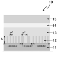
- FIG. 1 A specific structural example of the current excitation type laser element is shown in FIG.
- 1 is a substrate
- 2 is an anode
- 3 is a hole injection layer
- 4 is a hole transport layer
- 5 is a light emitting layer
- 6 is an electron transport layer
- 7 is a cathode.
- the laser light generated in the light emitting layer may pass through the anode and be taken out to the outside, or may pass through the cathode and be taken out to the outside, and may pass through the anode and the cathode and be taken out to the outside. It may be taken out. Further, the laser light generated in the light emitting layer may be taken out from the end face of the organic layer.
- each member and each layer of the current excitation type laser element will be described. The description of the substrate and the light emitting layer also applies to the substrate and the light emitting layer of the photoexcited laser element.
- the current-excited laser device of the present invention is preferably supported by a substrate.
- a substrate when the current excitation type laser element is configured to extract the laser light from the substrate side, a substrate having translucency to the laser light is used, and a transparent substrate made of glass, transparent plastic, quartz, or the like is used. Is preferably used.
- the substrate when the current excitation type laser element has a configuration in which laser light is extracted from the side opposite to the substrate, the substrate is not particularly limited, and a substrate made of silicon, paper, or cloth may be used in addition to the above transparent substrate. it can.
- anode As the anode in the current excitation type laser element, a metal having a large work function (4 eV or more), an alloy, an electrically conductive compound, or a mixture thereof as an electrode material is preferably used.
- electrode materials include metals such as Au, and conductive transparent materials such as CuI, indium zinc oxide (ITO), SnO 2, ZnO, and TiN.
- a material capable of producing an amorphous transparent conductive film such as IDIXO (In 2 O 3-ZnO) may be used.
- the anode can be formed by forming a film of these electrode materials by a method such as vapor deposition or sputtering.
- a pattern having a desired shape may be formed on the formed thin film by a photolithography method to serve as an anode, or when pattern accuracy is not required so much (about 100 ⁇ m or more), it is desired at the time of vapor deposition or sputtering of the electrode material.
- the pattern may be formed through a mask having the shape of.
- a coatable material such as an organic conductive compound
- a wet film forming method such as a printing method or a coating method can also be used.
- the current excitation type laser element is configured to transmit the laser light through the anode, the anode needs to have translucency with respect to the laser light, and the transmittance of the laser light is 1.
- the film thickness depends on the material, but is usually selected in the range of 10 to 1000 nm, preferably 10 to 200 nm.
- cathode a metal having a smaller work function than the material used for the anode (referred to as an electron-injectable metal), an alloy, an electrically conductive compound, or a mixture thereof is used as an electrode material.
- electrode materials include sodium, sodium-potassium alloy, magnesium, lithium, magnesium / copper mixture, magnesium / silver mixture, magnesium / aluminum mixture, magnesium / indium mixture, aluminum / aluminum oxide (Al 2 O). 3 ) Examples thereof include a mixture, indium, a lithium / aluminum mixture, aluminum, and a rare earth metal.
- a mixture of an electron injectable metal and a second metal which is a stable metal having a larger work function value than this for example, a magnesium / silver mixture.
- a magnesium / silver mixture Magnesium / aluminum mixture, magnesium / indium mixture, aluminum / aluminum oxide (Al 2 O 3 ) mixture, lithium / aluminum mixture, aluminum and the like are suitable.
- the cathode can be formed by forming a film of these electrode materials by a method such as vapor deposition or sputtering.
- the cathode needs to have translucency with respect to the laser light, and the transmittance of the laser light is 1. It is preferably configured to be greater than%, and more preferably configured to be greater than 10%. Specifically, it is preferable to use a thin film formed by forming the above electrode material with a thickness of 10 to 100 nm as the cathode.
- a laminated film in which an electrode made of a conductive transparent material such as indium tin oxide (ITO) illustrated in the above (anode) column and an organic layer containing an electron injectable material such as cesium (Cs) are laminated is also a cathode. Can be used as.
- the sheet resistance as a cathode is preferably several hundred ⁇ / ⁇ or less, and the film thickness is usually selected in the range of 10 nm to 5 ⁇ m, preferably 50 to 200 nm.
- the light emitting layer is a layer that emits laser light after holes and electrons injected from the anode and the cathode are recombined to generate excitons and a population inversion is formed.
- the light emitting material (laser oscillation material) of the light emitting layer one kind or two or more kinds selected from the compound group represented by the general formula (1) can be used.
- the light emitting layer may contain only the compound represented by the general formula (1), but may also contain other materials such as a lasing sensitizer and a host material. Preferable examples of other materials include compounds represented by the general formula (2).
- the compound represented by the general formula (2) is represented by the general formula (1) because the light emitting layer contains the compound represented by the general formula (1) and the compound represented by the general formula (2). It effectively functions as a laser sensitizer that promotes the light emission process of the compound, and can improve the laser oscillation characteristics.
- the light emitting layer one kind or two or more kinds selected from the compound group represented by the general formula (2) can be used.
- the laser light is emitted from the compound represented by the general formula (1) contained as a light emitting material. This laser light may be spontaneous emission amplified light or stimulated emission light induced and emitted by light emitted from the outside. Further, the light from the light emitting layer may include light emitted from the compound represented by the general formula (2).
- the content of the compound represented by the general formula (1) in the light emitting layer is 0.01 to 10% by weight and is represented by the general formula (2). It is preferable that the content of the compound is larger than the content of the compound represented by the general formula (1).
- the content of the compound represented by the general formula (1) in the light emitting layer can be, for example, 0.1% by weight or more, 0.5% by weight or more, and 90% by weight or less, 50. It can be less than% by weight.
- the injection layer is a layer provided between the electrode and the organic layer in order to reduce the driving voltage and improve the emission brightness.
- the injection layer can be provided as needed.
- the blocking layer is a layer capable of blocking the diffusion of charges (electrons or holes) and / or excitons existing in the light emitting layer to the outside of the light emitting layer.
- the electron blocking layer can be arranged between the light emitting layer and the hole transporting layer to prevent electrons from passing through the light emitting layer toward the hole transporting layer.
- the hole blocking layer can be placed between the light emitting layer and the electron transporting layer to prevent holes from passing through the light emitting layer towards the electron transporting layer.
- the blocking layer can also be used to prevent excitons from diffusing outside the light emitting layer. That is, the electron blocking layer and the hole blocking layer can also function as exciton blocking layers, respectively.
- the electron blocking layer or exciton blocking layer referred to in the present specification is used in the sense that one layer includes a layer having the functions of an electron blocking layer and an exciton blocking layer.
- the hole blocking layer has a function of an electron transporting layer in a broad sense.
- the hole blocking layer has a role of blocking the holes from reaching the electron transporting layer while transporting electrons, which can improve the recombination probability of electrons and holes in the light emitting layer.
- As the material of the hole blocking layer a material of the electron transport layer described later can be used as needed.
- the electron blocking layer has a function of transporting holes in a broad sense.
- the electron blocking layer has a role of blocking electrons from reaching the hole transporting layer while transporting holes, which can improve the probability that electrons and holes are recombined in the light emitting layer. ..
- the exciton blocking layer is a layer for preventing excitons generated by the recombination of holes and electrons in the light emitting layer from diffusing into the charge transport layer, and the exciton is inserted by inserting this layer. It is possible to efficiently confine it in the light emitting layer, and it is possible to improve the light emitting efficiency of the element.
- the exciton blocking layer can be inserted into either the anode side or the cathode side adjacent to the light emitting layer, and both can be inserted at the same time.
- the layer when the exciton blocking layer is provided on the anode side, the layer can be inserted between the hole transport layer and the light emitting layer adjacent to the light emitting layer, and when inserted on the cathode side, the light emitting layer and the cathode can be inserted.
- the layer can be inserted adjacent to the light emitting layer between and.
- a hole injection layer, an electron blocking layer, or the like can be provided between the anode and the exciton blocking layer adjacent to the anode side of the light emitting layer, and the cathode and the excitation adjacent to the cathode side of the light emitting layer can be provided.
- An electron injection layer, an electron transport layer, a hole blocking layer, and the like can be provided between the child blocking layer and the electron blocking layer.
- the blocking layer it is preferable that at least one of the excited singlet energy and the excited triplet energy of the material used as the blocking layer is higher than the excited singlet energy and the excited triplet energy of the light emitting material.
- the hole transport layer is made of a hole transport material having a function of transporting holes, and the hole transport layer may be provided with a single layer or a plurality of layers.
- the hole transporting material has either injection or transport of holes or an electron barrier property, and may be either an organic substance or an inorganic substance.
- Known hole transporting materials that can be used include, for example, triazole derivatives, oxadiazole derivatives, imidazole derivatives, carbazole derivatives, indolocarbazole derivatives, polyarylalkane derivatives, pyrazoline derivatives and pyrazolone derivatives, phenylenediamine derivatives, arylamine derivatives, etc.
- Amino-substituted chalcone derivatives oxazole derivatives, styrylanthracene derivatives, fluorenone derivatives, hydrazone derivatives, stilben derivatives, silazane derivatives, aniline copolymers, conductive polymer oligomers, especially thiophene oligomers, etc. It is preferable to use a group tertiary amine compound and a styrylamine compound, and it is more preferable to use an aromatic tertiary amine compound.
- the electron transport layer is made of a material having a function of transporting electrons, and the electron transport layer may be provided with a single layer or a plurality of layers.
- the electron transporting material (which may also serve as a hole blocking material) may have a function of transmitting electrons injected from the cathode to the light emitting layer.
- Examples of the electron transporting layer that can be used include nitro-substituted fluorene derivatives, diphenylquinone derivatives, thiopyrandioxide derivatives, carbodiimides, freolenidenemethane derivatives, anthracinodimethane and anthrone derivatives, and oxadiazole derivatives.
- a thiadiazole derivative in which the oxygen atom of the oxadiazole ring is replaced with a sulfur atom, and a quinoxalin derivative having a quinoxalin ring known as an electron-withdrawing group can also be used as an electron transport material.
- a polymer material in which these materials are introduced into a polymer chain or these materials are used as a polymer main chain can also be used.
- the current-excited laser device of the present invention may further have a resonator structure.
- the "resonator structure” is a structure for reciprocating the light emitted by the light emitting material in the light emitting layer. As a result, the light repeatedly travels in the light emitting layer to cause stimulated emission, so that a higher intensity laser beam can be obtained.
- the resonator structure is specifically composed of a pair of reflectors, one of which preferably has a reflectance of 100% and the other of which has a reflectance of 50-95%. preferable. By setting the reflectance of the other reflector to be relatively low, it is possible to allow the laser beam to pass through the reflector and take out the laser beam to the outside.
- the reflecting mirror on the side that extracts the laser beam is referred to as an "output mirror".
- the reflector and the output mirror may be provided separately from each layer and each part constituting the above-mentioned current-excited laser element, or the anode and cathode may also have the function of the reflector or the output mirror.
- the anode when the anode also functions as a reflector or an output mirror, the anode is made of a metal film having a small absorption of visible light, a high reflectance, and a relatively large work function (4.0 eV or more). It is preferable to configure it.
- a metal film include a metal film such as Ag, Pt, and Au, or an alloy film containing these metals.
- the reflectance and transmittance of the anode can be adjusted to desired values by controlling the film thickness of the metal film, for example, in the range of several tens of nm or more.
- the cathode When the cathode also functions as a reflector or an output mirror, the cathode is preferably formed of a metal film having a small absorption of visible light, a high reflectance, and a relatively small work function. Examples of such a metal film include a metal film such as Al and Mg, or an alloy film containing these metals.
- the reflectance and transmittance of the cathode can be adjusted to desired values by controlling the film thickness of the metal film, for example, in the range of several tens of nm or more.
- a reflector or an output mirror is provided separately from each of the above layers and parts, a reflective film is formed between the anode and the organic layer or between the substrate and the anode to form a reflector or an output mirror.
- a reflector or an output mirror is provided between the anode and the organic layer, as those materials, the absorption of visible light is small, high reflectance can be obtained, and the work function is large (work function 4.0 eV). Above) It is preferable to use a conductive material. Specifically, a metal film made of a metal such as Ag, Pt, Au, or an alloy containing these metals can be used as a reflector or an output mirror. The reflectance and transmittance of this reflector or output mirror can be adjusted to desired values by controlling the film thickness of the metal film, for example, in the range of several tens of nm or more.
- the material of the anode does not need to have a large work function, and a known electrode material can be widely used.
- a reflector or an output mirror is provided between the substrate and the anode, it is preferable to use a material having low visible light absorption and high reflectance.
- a dielectric multilayer film or the like formed on the above can be used as a reflecting mirror or an output mirror.
- the reflectance and transmittance of the metal film can be adjusted to desired values by controlling the film thickness in the range of, for example, several tens of nm or more. Further, the reflectance and transmittance of the dielectric multilayer film can be adjusted to desired values by controlling the film thickness and the number of layers of silicon oxide and titanium oxide.
- the combination of the reflector and the output mirror is a combination in which the output mirror is the anode and the reflector is the cathode, and the output mirror is a reflective film arranged between the anode and the organic layer or between the substrate and the anode.
- the reflector is the cathode
- the reflector is the anode and the output mirror is the cathode
- the reflector is a reflective film placed between the anode and the organic layer or between the substrate and the anode.
- the output mirror is a cathode
- the total optical film thickness of the layers interposed between the reflector and the output mirror is an integer of the half wavelength of the laser beam. It is preferable to design the layer structure of the element so as to be doubled. As a result, a standing wave is formed between the reflecting mirror and the output mirror, the light is amplified, and a higher intensity laser beam can be obtained.
- the above resonator structure reciprocates the laser beam in the direction perpendicular to the main surface of the substrate, but the resonator structure reciprocates the laser beam in the horizontal direction with respect to the main surface of the substrate.
- the end face of the organic layer can be configured as a reflector or an output mirror by utilizing the reflection due to the difference in the refractive index between the organic layer and air.
- a diffraction grating is provided near the light emitting layer at a lattice spacing of ⁇ / 2n ( ⁇ : wavelength of light, an integer of n: 1 or more), and the light generated in the light emitting layer is periodically reflected by the lattice spacing of the diffraction grating. You may let it. As a result, a single longitudinal mode can be realized, and a laser beam having good monochromaticity can be emitted from the end face of the organic layer.
- the current excitation type laser element as described above emits laser light by passing a current equal to or higher than the threshold current density between the anode and the cathode.
- excellent laser oscillation characteristics can be obtained by including the compound represented by the general formula (1) in the light emitting layer. Further, by including the compound represented by the general formula (2), the laser oscillation characteristics can be improved.
- the compound represented by the general formula (1) and the compound represented by the general formula (2) are used for the light emitting layer, but also a layer other than the light emitting layer is used. It may also be used for.
- the compound represented by (2) may be the same or different.
- the above-mentioned injection layer, blocking layer, hole blocking layer, electron blocking layer, exciton blocking layer, hole transporting layer, electron transporting layer and the like are also compound represented by the general formula (1) or the general formula (2).
- the film forming method of these layers is not particularly limited, and may be formed by either a dry process or a wet process.
- R 21 and R 25 each independently represent a substituent having a positive Hammett ⁇ p value
- R 23 represents a substituent
- R 22 , R 24 , and R 26 to R 35 are independent of each other.
- R 21 and R 25 are cyano groups
- R 23 is a substituted aryl group or a substituted or unsubstituted heteroaryl group.
- R 23 is preferably a substituted or unsubstituted aryl group, a substituted or unsubstituted heteroaryl group, R 36 CO- (R 36 represents a hydrogen atom or a substituent), or a halogen atom.
- R 23 a substituted aryl group can be specifically selected.
- a halogen atom can be particularly selected as R 23.
- R 36 CO- can be particularly selected as R 23.
- the compound represented by the general formula (3) is useful as a material for the light emitting layer of the laser device. Further, the compound in which R 23 of the general formula (3) is a halogen atom is also useful as a raw material for synthesizing a compound having a substituent other than the halogen atom in R 23. In particular , a compound in which R 21 and R 25 are cyano groups and R 23 is a halogen atom is also useful as a synthetic raw material for a compound represented by the following general formula (4).
- R 43 represents a substituted aryl group or a substituted or unsubstituted heteroaryl group
- R 42 , R 44 , and R 46 to R 55 each independently represent a hydrogen atom or a substituent.
- Descriptions of R 42 , R 44 , R 46 to R 55 of the general formula (4), preferable ranges, and specific examples are described for R 2 , R 4 , and R 6 to R 15 of the general formula (1), respectively. Can be referred to.
- X represents a halogen atom, and examples thereof include a fluorine atom, a chlorine atom, a bromine atom, and an iodine atom.
- a chlorine atom, a bromine atom, and an iodine atom are preferable, and a bromine atom is more preferable.
- N-bromosuccinimide can be used as the brominating agent for introducing a bromine atom.
- the above reaction is an application of a selective electrophilic substitution reaction at the 4-position of phosphinin and a known coupling reaction such as a Suzuki coupling reaction, and known reaction conditions can be appropriately selected and used.
- a known coupling reaction such as a Suzuki coupling reaction
- known reaction conditions can be appropriately selected and used.
- the lasing sensitizer of the present invention contains a compound represented by the general formula (2).
- the description in the column of [Compound represented by the general formula (2)] can be referred to.
- the compound represented by the general formula (2) has a property that the excited singlet energy obtained by light absorption can be easily transferred to the light emitting material and the excited triplet energy generated by the intersystem crossing of the light emitting material can be easily received. Therefore, the compound represented by the general formula (2) promotes the transition of the light emitting material to the photoexcited singlet state and the formation of the population inversion, and acts to suppress the singlet-triplet annihilation in the light emitting material. Therefore, the laser oscillation characteristics of the light emitting material can be improved. Therefore, the compound represented by the general formula (2) is useful as a lasing sensitizer.
- the laser element (second laser element) of the present invention is a laser element having a light emitting layer containing a lasing sensitizer and a light emitting material.
- the lasing sensitizer contains the compound represented by the above general formula (2).
- the description in the column of [Compound represented by the general formula (2)] can be referred to, and the general formula (2) can be used.
- the action of the represented compound as a lasing sensitizer refer to the description in the above column (compound represented by the general formula (2)) and the description in the ⁇ raising sensitizer> column. Can be done.
- the luminescence-excited singlet energy level of the luminescent material is lower than the luminescence-excited singlet energy level of the lasing sensitizer, and the luminescence-excited triplet energy level of the luminescent material is lasing. Higher than the luminescence-excited triplet energy level of the sensitizer.
- the excited singlet energy obtained by light absorption of the compound represented by the general formula (2) can be transferred to the emission-excited singlet energy level of the light-emitting material by the Felster movement mechanism, and also emit light.
- the excited triplet energy generated by the crossing between the terms of the material can be transferred to the emission-excited triplet energy level of the compound represented by the general formula (2) by the Dexter transfer mechanism.
- the lasing sensitizer functions more effectively, and the laser oscillation characteristics can be improved.
- the description in the column of [Energy relationship between the compound represented by the general formula (1) and the compound represented by the general formula (2)] is expressed by the "general formula (1)". It can be referred to by replacing "compound” with "light emitting material".
- the light emitting material is a compound capable of emitting spontaneous emission amplified light or stimulated emission light, and can be used without limitation as long as it exhibits the above energy relationship.
- the layer structure of the second laser device the above description in the [Laser device layer structure] column may be referred to by replacing "compound represented by the general formula (1)" with "light emitting material”. it can.
- the emission characteristics are evaluated by a fluorescence spectrophotometer (manufactured by Nippon Spectrometer Co., Ltd .: FP-8600), an absolute PL quantum yield measuring device (manufactured by Hamamatsu Photonics Co., Ltd .: C11347-01), and a multi-channel spectroscope (manufactured by Hamamatsu Photonics Co., Ltd.). : PMA-12) was used.
- Diphenyltrimethylsilylphosphine (11.55 g, 44.7 mmol) was dissolved in chloroacetonitrile (16.8 g, 5.0 eq) and stirred at 60 ° C. for 48 hours. The mixture was cooled and the precipitated precipitate was filtered off to give a yellow solid. The yellow solid was washed with chloroform and diethyl ether and dried under reduced pressure at 70 ° C. for 2 hours to obtain a white solid of Intermediate 1 in a yield of 9.84 g and a yield of 73%.
- 1,1,3,3-tetramethoxypropane (5.01 g, 30.5 mmol) and aniline (5.80 g, 62.3 mmol) were dissolved in ethanol (60 mL) and cooled to 0 ° C. Concentrated hydrochloric acid (6 mL) was added to this mixture, the temperature was returned to room temperature, and the mixture was stirred for 16 hours. This reaction solution was concentrated under reduced pressure, and the precipitated precipitate was filtered off to obtain a yellow solid. By recrystallizing this yellow solid with methanol, the yellow solid of Intermediate 2 was obtained in a yield of 6.12 g and a yield of 90%.
- the obtained residue was crudely purified by silica gel calm chromatography using chloroform as an eluent, and recrystallized from a mixed solvent of chloroform and diethyl ether to yield a red-orange solid of intermediate 3 in a yield of 1.17 g. Obtained at a rate of 88%.
- the obtained residue was crudely purified by silica gel calm chromatography using ethyl acetate / trichloromethane (1/2) as an eluent, and recrystallized from a mixed solvent of chloroform and diethyl ether to form a yellow solid compound 13.
- the energy levels E (B) T1 are shown in Table 1.
- a thin film of compound 1 (single film) and a thin film of compound B1 (single film) were formed on a quartz substrate with a thickness of 200 nm under the condition of a vacuum degree of 10 -4 Pa or less. Further, a thin film (mixed film) is formed with a thickness of 200 nm by co-depositing compound 1 and compound B1 from different vapor deposition sources on a quartz substrate under the condition of a vacuum degree of 10 -4 Pa or less by a vacuum vapor deposition method. did. At this time, the concentration of compound 1 was set to 0.5% by weight or 1.0% by weight, and two types of mixed films having different concentrations of compound 1 were formed. Further, a polymer film composed of compound 1 and polymethylmethacrylate (PMMA) was formed on a quartz substrate with a thickness of 200 nm by a spin coating method. At this time, the concentration of compound 1 was 1.0% by weight.
- PMMA polymethylmethacrylate
- the luminescence of the mixed film was the luminescence derived from Compound 1.
- the phosphorescence spectrum of the mixed film was measured at 77K, no phosphorescence was observed. From this, it was shown that the excitons generated in compound 1 by the energy received from compound B1 are mainly singlet excitons.
- Table 2 shows the rate (PLQY) and the radiation attenuation constant.
- the wavelength range of 350 to 420 nm is dominated by the emission of compound B1
- the wavelength range of 550 to 700 nm is dominated by the emission of compound 1. Area.
- the polymer membrane containing compound 1 and the mixed membrane of compound 1 and compound B1 all showed high PLQY, but the PLQY of the mixed membrane was higher than that of the polymer membrane. ..
- the high PLQY it was achieved mixed film of Compound 1 and Compound B1, the light-emitting excited singlet energy level E S1 of Compound 1 emission excited singlet energy level E of Compound B1 (B) S1 lower than (E S1 ⁇ E (B) S1), also emission excitation triplet energy level E T1 of compound 1 is higher than the emission excitation triplet energy level E (B) T1 of compound B1 (E T1 > E (B) T1 ), it is presumed that the following mechanism worked.
- the luminescence-excited triplet state since the luminescence-excited triplet state has a long life, if there is no destination for its energy, it accumulates there and becomes dense, causing singlet-triplet annihilation and reducing PLQY. Will end up.
- ET1 > E (B) T1 the excited triplet energy of compound 1 moves to the emission-excited triplet energy level E (B) T1 of compound B1 by the Dexter transfer mechanism. , Accumulation of excited triplet state in compound 1 is suppressed.
- the singlet-triplet annihilation induced by the accumulation of excited triplet states was also suppressed, and it is presumed that high PLQY was obtained.
- the compound represented by the general formula (2) when the compound represented by the general formula (1) and the compound represented by the general formula (2) satisfy the above energy relationship, the compound represented by the general formula (2) is excited. Since it also functions as a quencher for quenching the triplet, the laser oscillation characteristics can be improved without adding another triplet quencher. This has the effect of simplifying the material design by eliminating the need for the addition of other triplet quenchers.
- the compound B1 used here has two vibrational levels at the emission-excited triple-term energy level E (B) T1 , but at least the lower vibrational level satisfies ET1 > E (B) T1. It is preferable that both the low level and the high vibration level (all vibration levels) satisfy this relationship.
- the half-value width of the ASE peak when the excitation light intensity is 2 ⁇ J / cm 2 is 3 nm or less at a 0.5% by mass concentration and 3 nm or less at a 1.0% by mass concentration, achieving a very narrow half-value width.
- the mixed membrane having a concentration of compound 1 of 0.5% by weight is irradiated with excitation light of 25.76 ⁇ J / cm 2 for a certain period of time, and the mixed membrane having a concentration of compound 1 of 1.0% by weight is 25.
- stable ASE intensity was shown for 5 hours or more.
- [3] Manufacture and evaluation of photoexcited laser element (Example 1)
- the laser element manufactured here has a layer structure shown in FIG. It is a distributed feedback type (DFB) photoexcited laser element having.
- the distributed feedback type photoexcited laser element 10 includes a glass substrate 11, a DFB lattice 12, a mixed layer (light emitting layer) 13 of compound 1 and compound B1, an amorphous layer (manufactured by AGC Asahi Glass Co., Ltd .: Cytop) 14, and a sapphire layer 15. It is laminated in this order.
- the laser element shown in FIG. 5 was manufactured as follows. On a glass substrate 11, SiO 2 layer was formed to a 65nm thick by sputtering. Subsequently, the SiO 2 layer was patterned using an electron beam lithography method and a reactive ion etching method to form a DFB lattice 12 in a region of 740 ⁇ m ⁇ 740 ⁇ m.
- the one-dimensional grating the grating period p 1 is 148 nm
- the two-dimensional grating the grating period p 2 is 296nm are arranged alternately
- the grating depth h is to form a mixed diffraction grating 65 nm.
- the lengths of the one-dimensional lattice forming region and the two-dimensional lattice forming region were set to 592 nm and 888 nm, respectively.
- a mixed film of compound 1 and compound B1 was formed to a thickness of 200 nm on the surface on which the DFB lattice was formed by using a co-evaporation method to form a light emitting layer 13.
- the concentration of compound 1 was 1% by weight.
- the amorphous layer 14 and the sapphire layer 15 as the protective layer were laminated in this order to form a DFB laser element (laser element 1).
- Example 2 Manufacture of a photoexcited laser element 2 having a one-dimensional lattice
- the laser element 2 is the same as in Example 1 except that only a one-dimensional lattice is formed instead of forming a mixed diffraction grating as a DFB lattice. Manufactured.
- Example 3 Manufacture of a photoexcited laser element 3 having a two-dimensional lattice
- the laser element 3 is the same as in Example 1 except that only a two-dimensional lattice is formed instead of forming a mixed diffraction grating as a DFB lattice. Manufactured.
- Table 3 shows the results of measuring the emission lifetime of the laser element 1 with the excitation light of 337 nm by changing the excitation intensity.
- excitation laser output is shown as a relative value with respect to a maximum output of 100 microJ / cm 2. The emission lifetime was determined by fitting the emission attenuation curve.
- the interference measurement between the short-distance field and the long-distance field was performed, and the beam cross section of the long-distance field was obtained by theoretical calculation. It was in good agreement with the cross section, and some interference fringes were observed in the close field pattern. From this, it was confirmed that the laser light from the laser element 1 is highly coherent light.
- the laser element manufactured here is shown in FIG. It is a distributed feedback type (DFB) current-pumped laser element having a layer structure.
- the distribution feedback type current excitation laser element 20 includes a glass substrate 21, a first electrode 22 made of indium tin oxide (ITO), a DFB lattice 23, a mixed layer 24 of cesium (Cs) and compound B1, and compound 1.
- a second electrode 27 made of a mixed layer (light emitting layer) 25 of compound B1, a molybdenum trioxide (MoO 3 ) layer 26, and aluminum (Al) is laminated in this order.
- the mixed layer of cesium and compound B1 functions as an electron injection layer that promotes electron injection into the light emitting layer
- the molybdenum oxide layer functions as a hole injection layer that promotes hole injection into the light emitting layer. ..
- the laser element shown in FIG. 6 was manufactured as follows. A glass substrate 21 on which the first electrode 22 made of ITO having a film thickness of 30 nm was formed was prepared. A SiO 2 layer was formed on the ITO by a sputtering method to a thickness of 65 nm.
- a DFB grating 23 as a mixed diffraction grating was formed in a region of 740 ⁇ m ⁇ 740 ⁇ m.
- each thin film was laminated on the surface on which the DFB lattice 23 was formed by a vacuum vapor deposition method at a vacuum degree of 10 -4 Pa.
- a mixed layer 25 of cesium and compound B1 was formed to a thickness of 30 nm between the lattices of the DFB lattice 23 by using a co-deposited method. At this time, the concentration of cesium was set to 20% by weight.
- a mixed film of compound 1 and compound B1 was formed to a thickness of 180 nm using a co-deposited method to form a light emitting layer 25. At this time, the concentration of compound 1 was 1% by weight. Subsequently, molybdenum trioxide 26 was formed to a thickness of 10 nm, and aluminum was further vapor-deposited to a thickness of 50 nm to form a second electrode 27, which was used as a DFB laser element (laser element 4).
- Example 5 Manufacture of a current-excited laser element 5 having a one-dimensional lattice
- the laser element is the same as in Example 1 except that only a one-dimensional lattice is formed instead of forming a mixed diffraction grating as a DFB lattice. 5 was manufactured.
- Example 6 Manufacture of a current-excited laser element 6 having a two-dimensional lattice
- the laser element is the same as in Example 1 except that only a two-dimensional lattice is formed instead of forming a mixed diffraction grating as a DFB lattice. 6 was manufactured.
- Reference Example Manufacture of Organic Electroluminescence Device
- a reference organic electroluminescence device (reference EL device) was manufactured in the same manner as in Example 1 except that a DFB lattice was not formed.
- the laser elements 4 and 6 and the reference EL element were measured at room temperature, under pulse conditions with a pulse width of 400 ns and a repetition frequency of 1 kHz, and the current density was changed in the range of 500 to 22200 mA / cm 2.
- the laser element was measured.
- No. 4 a phenomenon is observed in which the half-value width of the emission peak is remarkably narrowed around 530 nm at a specific current density or more, and in the laser element 6, the half-value width of the emission peak is remarkably narrowed around 505 nm at a specific current density or more. The phenomenon of narrowing was observed.
- the reference EL element the remarkable narrowing of the half width as seen in the laser elements 4 and 6 was not observed.
- the compound of the present invention is a new laser oscillation material having a skeletal structure different from that of BSBCz. Therefore, by using this compound in the laser element, various emission wavelengths and oscillation characteristics can be realized, and the versatility of the organic laser element can be improved. Therefore, the present invention has high industrial applicability.
- Substrate 2 Anode 3 Hole injection layer 4 Hole transport layer 5 Light emitting layer 6 Electron transport layer 7 Cathode 11, 21 Glass substrate 12, 23 DFB lattice 13, 25 Light emitting layer 14 Amorphous layer 15 Sapphire layer 22 First electrode 24 Cesium And compound B1 mixed layer 26 molybdenum trioxide layer 27 second electrode
Landscapes
- Chemical & Material Sciences (AREA)
- Physics & Mathematics (AREA)
- Engineering & Computer Science (AREA)
- Materials Engineering (AREA)
- Spectroscopy & Molecular Physics (AREA)
- Organic Chemistry (AREA)
- Electromagnetism (AREA)
- Optics & Photonics (AREA)
- Molecular Biology (AREA)
- Health & Medical Sciences (AREA)
- General Health & Medical Sciences (AREA)
- Condensed Matter Physics & Semiconductors (AREA)
- General Physics & Mathematics (AREA)
- Biochemistry (AREA)
- Life Sciences & Earth Sciences (AREA)
- Plasma & Fusion (AREA)
- Dispersion Chemistry (AREA)
- Electroluminescent Light Sources (AREA)
- Semiconductor Lasers (AREA)
- Plural Heterocyclic Compounds (AREA)
Priority Applications (5)
| Application Number | Priority Date | Filing Date | Title |
|---|---|---|---|
| EP20871785.0A EP4039772A4 (en) | 2019-09-30 | 2020-09-25 | Laser element, compound, method for producing compound and lasing sensitizer |
| KR1020227005485A KR20220075307A (ko) | 2019-09-30 | 2020-09-25 | 레이저 소자, 화합물, 화합물의 제조 방법, 레이징 증감제 |
| JP2021551187A JP7580705B2 (ja) | 2019-09-30 | 2020-09-25 | レーザー素子、化合物、化合物の製造方法、レージング増感剤 |
| US17/765,242 US20220294190A1 (en) | 2019-09-30 | 2020-09-25 | Laser element, compound, method for producing compound and lasing sensitizer |
| CN202080067864.9A CN114450814A (zh) | 2019-09-30 | 2020-09-25 | 激光元件、化合物、化合物的制造方法、激光增感剂 |
Applications Claiming Priority (2)
| Application Number | Priority Date | Filing Date | Title |
|---|---|---|---|
| JP2019178599 | 2019-09-30 | ||
| JP2019-178599 | 2019-09-30 |
Publications (1)
| Publication Number | Publication Date |
|---|---|
| WO2021065725A1 true WO2021065725A1 (ja) | 2021-04-08 |
Family
ID=75336515
Family Applications (1)
| Application Number | Title | Priority Date | Filing Date |
|---|---|---|---|
| PCT/JP2020/036305 Ceased WO2021065725A1 (ja) | 2019-09-30 | 2020-09-25 | レーザー素子、化合物、化合物の製造方法、レージング増感剤 |
Country Status (7)
| Country | Link |
|---|---|
| US (1) | US20220294190A1 (https=) |
| EP (1) | EP4039772A4 (https=) |
| JP (1) | JP7580705B2 (https=) |
| KR (1) | KR20220075307A (https=) |
| CN (1) | CN114450814A (https=) |
| TW (1) | TW202144374A (https=) |
| WO (1) | WO2021065725A1 (https=) |
Cited By (2)
| Publication number | Priority date | Publication date | Assignee | Title |
|---|---|---|---|---|
| US20220181555A1 (en) * | 2020-12-04 | 2022-06-09 | National University Corporation Ehime University | Light-emitting material for organic light-emitting diode, blue light-emitting material for organic light-emitting diode, and organic light-emitting diode |
| WO2024101343A1 (ja) * | 2022-11-11 | 2024-05-16 | 株式会社フラスク | 有機el用発光材料、有機el用青色発光材料、及び有機el素子 |
Citations (8)
| Publication number | Priority date | Publication date | Assignee | Title |
|---|---|---|---|---|
| JP2003142263A (ja) * | 2001-10-30 | 2003-05-16 | Matsushita Electric Ind Co Ltd | 発光素子およびこれを用いた装置 |
| US20130066092A1 (en) * | 2010-02-11 | 2013-03-14 | Rafal Czerwieniec | Use of gold complexes in optoelectronic devices |
| JP2015201463A (ja) * | 2012-08-07 | 2015-11-12 | 国立大学法人九州大学 | 有機エレクトロルミネッセンス素子、並びに、それに用いる化合物、キャリア輸送材料およびホスト材料 |
| JP2018035124A (ja) * | 2016-09-02 | 2018-03-08 | 国立大学法人九州大学 | 有機発光素子ならびにそれに用いる発光材料および化合物 |
| JP2018512726A (ja) * | 2015-02-18 | 2018-05-17 | ノヴァレッド ゲーエムベーハー | 半導体材料および半導体材料用のナフトフランマトリクス化合物 |
| WO2018155642A1 (ja) * | 2017-02-24 | 2018-08-30 | 国立大学法人九州大学 | 化合物、発光材料および発光素子 |
| JP2018174279A (ja) * | 2017-03-31 | 2018-11-08 | 国立大学法人九州大学 | 有機半導体レーザー素子 |
| WO2019176971A1 (ja) * | 2018-03-13 | 2019-09-19 | 国立大学法人九州大学 | 電荷輸送材料、化合物および有機発光素子 |
Family Cites Families (2)
| Publication number | Priority date | Publication date | Assignee | Title |
|---|---|---|---|---|
| JP5493708B2 (ja) * | 2009-10-28 | 2014-05-14 | 三菱化学株式会社 | 電子写真感光体、電子写真カートリッジ及び画像形成装置 |
| DE102010018321A1 (de) * | 2010-04-27 | 2011-10-27 | Merck Patent Gmbh | Organische Elektrolumineszenzvorrichtung |
-
2020
- 2020-09-25 EP EP20871785.0A patent/EP4039772A4/en not_active Withdrawn
- 2020-09-25 US US17/765,242 patent/US20220294190A1/en not_active Abandoned
- 2020-09-25 KR KR1020227005485A patent/KR20220075307A/ko not_active Withdrawn
- 2020-09-25 CN CN202080067864.9A patent/CN114450814A/zh active Pending
- 2020-09-25 WO PCT/JP2020/036305 patent/WO2021065725A1/ja not_active Ceased
- 2020-09-25 JP JP2021551187A patent/JP7580705B2/ja active Active
- 2020-10-05 TW TW109134453A patent/TW202144374A/zh unknown
Patent Citations (8)
| Publication number | Priority date | Publication date | Assignee | Title |
|---|---|---|---|---|
| JP2003142263A (ja) * | 2001-10-30 | 2003-05-16 | Matsushita Electric Ind Co Ltd | 発光素子およびこれを用いた装置 |
| US20130066092A1 (en) * | 2010-02-11 | 2013-03-14 | Rafal Czerwieniec | Use of gold complexes in optoelectronic devices |
| JP2015201463A (ja) * | 2012-08-07 | 2015-11-12 | 国立大学法人九州大学 | 有機エレクトロルミネッセンス素子、並びに、それに用いる化合物、キャリア輸送材料およびホスト材料 |
| JP2018512726A (ja) * | 2015-02-18 | 2018-05-17 | ノヴァレッド ゲーエムベーハー | 半導体材料および半導体材料用のナフトフランマトリクス化合物 |
| JP2018035124A (ja) * | 2016-09-02 | 2018-03-08 | 国立大学法人九州大学 | 有機発光素子ならびにそれに用いる発光材料および化合物 |
| WO2018155642A1 (ja) * | 2017-02-24 | 2018-08-30 | 国立大学法人九州大学 | 化合物、発光材料および発光素子 |
| JP2018174279A (ja) * | 2017-03-31 | 2018-11-08 | 国立大学法人九州大学 | 有機半導体レーザー素子 |
| WO2019176971A1 (ja) * | 2018-03-13 | 2019-09-19 | 国立大学法人九州大学 | 電荷輸送材料、化合物および有機発光素子 |
Non-Patent Citations (7)
| Title |
|---|
| AIMONO ET AL.: "100% fluorescence efficiency of 4,4'-bis[(N-carbazole)styryl]biphenyl in a solid film and the very low amplified spontaneous emission threshold", APPLIED PHYSICS LETTERS, vol. 86, no. 7, 9 February 2005 (2005-02-09), pages 071110-1 - 071110-3, XP012066316 * |
| APPL. PHYS. LETT., vol. 86, 2005, pages 071110 |
| HANSCH, C., CHEM. REV., vol. 91, 1991, pages 165 - 195 |
| HASHIMOTO ET AL.: "Synthesis and Photophysical Properties of A5-Phosphinines as a Tunable Fluorophore", JOURNAL OF THE AMERICAN CHEMICAL SOCIETY, vol. 140, no. 6, 14 February 2018 (2018-02-14), pages 2046 - 2049, XP055811504 * |
| SCHAFER ET AL.: "Nature of Bonding in À5- Phosphorins", JOURNAL OF THE AMERICAN CHEMICAL SOCIETY, vol. 98, no. 15, 21 July 1976 (1976-07-21), pages 4410 - 4418, XP002649741 * |
| See also references of EP4039772A4 |
| SVYASCHENKO ET AL.: "Electrocyclization of Phosphahexatrienes: An Approach to λ5-Phosphinines", THE JOURNAL OF ORGANIC CHEMISTRY, vol. 76, no. 15, 5 August 2011 (2011-08-05), pages 6125 - 6133, XP055811505 * |
Cited By (2)
| Publication number | Priority date | Publication date | Assignee | Title |
|---|---|---|---|---|
| US20220181555A1 (en) * | 2020-12-04 | 2022-06-09 | National University Corporation Ehime University | Light-emitting material for organic light-emitting diode, blue light-emitting material for organic light-emitting diode, and organic light-emitting diode |
| WO2024101343A1 (ja) * | 2022-11-11 | 2024-05-16 | 株式会社フラスク | 有機el用発光材料、有機el用青色発光材料、及び有機el素子 |
Also Published As
| Publication number | Publication date |
|---|---|
| CN114450814A (zh) | 2022-05-06 |
| JP7580705B2 (ja) | 2024-11-12 |
| TW202144374A (zh) | 2021-12-01 |
| KR20220075307A (ko) | 2022-06-08 |
| JPWO2021065725A1 (https=) | 2021-04-08 |
| EP4039772A1 (en) | 2022-08-10 |
| US20220294190A1 (en) | 2022-09-15 |
| EP4039772A4 (en) | 2023-01-25 |
Similar Documents
| Publication | Publication Date | Title |
|---|---|---|
| JP7758385B2 (ja) | 化合物、発光材料および発光素子 | |
| JP7076699B2 (ja) | 発光材料、化合物および有機発光素子 | |
| JP6318155B2 (ja) | 化合物、発光材料および有機発光素子 | |
| JP5594750B2 (ja) | 化合物、発光材料および有機発光素子 | |
| JP6277182B2 (ja) | 化合物、発光材料および有機発光素子 | |
| JP6466913B2 (ja) | 発光材料、有機発光素子および化合物 | |
| JP7410571B2 (ja) | 化合物、発光材料、遅延蛍光体、有機発光素子、酸素センサー、分子の設計方法およびプログラム | |
| JPWO2018159662A1 (ja) | 化合物、発光材料および有機発光素子 | |
| JPWO2015002213A1 (ja) | 発光材料、遅延蛍光体、有機発光素子および化合物 | |
| WO2015080183A1 (ja) | 発光材料、有機発光素子および化合物 | |
| KR20150016242A (ko) | 발광 재료 및 유기 발광 소자 | |
| CN110582905B (zh) | 有机半导体激光元件 | |
| JP7580705B2 (ja) | レーザー素子、化合物、化合物の製造方法、レージング増感剤 | |
| WO2017155102A1 (ja) | 発光材料、有機発光素子および化合物 | |
| JP7395136B2 (ja) | 組成物および有機発光素子 | |
| JP7709649B2 (ja) | 有機エレクトロルミネッセンス素子、薄膜、化合物、遅延蛍光発光体および有機半導体レーザー | |
| JPWO2020175624A1 (ja) | 化合物、発光材料および有機半導体レーザー素子 | |
| WO2018159663A1 (ja) | 発光材料、有機発光素子および化合物 | |
| WO2025027974A1 (ja) | 有機エレクトロルミネッセンス素子及び電子機器 | |
| JPWO2020130086A1 (ja) | 分解抑制剤、薄膜、レーザー発振素子およびレーザー色素の分解抑制方法 | |
| JP2016084283A (ja) | 化合物、発光材料および有機発光素子 |
Legal Events
| Date | Code | Title | Description |
|---|---|---|---|
| 121 | Ep: the epo has been informed by wipo that ep was designated in this application |
Ref document number: 20871785 Country of ref document: EP Kind code of ref document: A1 |
|
| ENP | Entry into the national phase |
Ref document number: 2021551187 Country of ref document: JP Kind code of ref document: A |
|
| NENP | Non-entry into the national phase |
Ref country code: DE |
|
| ENP | Entry into the national phase |
Ref document number: 2020871785 Country of ref document: EP Effective date: 20220502 |