WO2021060058A1 - Film de résine, dispositif électronique, procédés de fabrication d'un film de résine et d'un dispositif électronique - Google Patents
Film de résine, dispositif électronique, procédés de fabrication d'un film de résine et d'un dispositif électronique Download PDFInfo
- Publication number
- WO2021060058A1 WO2021060058A1 PCT/JP2020/034784 JP2020034784W WO2021060058A1 WO 2021060058 A1 WO2021060058 A1 WO 2021060058A1 JP 2020034784 W JP2020034784 W JP 2020034784W WO 2021060058 A1 WO2021060058 A1 WO 2021060058A1
- Authority
- WO
- WIPO (PCT)
- Prior art keywords
- resin film
- chemical formula
- carbon atoms
- film
- polyimide
- Prior art date
Links
- 229920005989 resin Polymers 0.000 title claims abstract description 282
- 239000011347 resin Substances 0.000 title claims abstract description 282
- 238000004519 manufacturing process Methods 0.000 title claims description 61
- 229920001721 polyimide Polymers 0.000 claims abstract description 122
- 239000004642 Polyimide Substances 0.000 claims abstract description 109
- 239000004065 semiconductor Substances 0.000 claims abstract description 79
- 230000008859 change Effects 0.000 claims abstract description 46
- 239000010408 film Substances 0.000 claims description 381
- 239000000126 substance Substances 0.000 claims description 124
- 125000004432 carbon atom Chemical group C* 0.000 claims description 76
- 238000000034 method Methods 0.000 claims description 57
- 239000011342 resin composition Substances 0.000 claims description 51
- 238000000576 coating method Methods 0.000 claims description 42
- 239000011248 coating agent Substances 0.000 claims description 39
- 238000010438 heat treatment Methods 0.000 claims description 38
- 150000000000 tetracarboxylic acids Chemical group 0.000 claims description 36
- 239000002243 precursor Substances 0.000 claims description 35
- 150000001875 compounds Chemical class 0.000 claims description 28
- 125000001183 hydrocarbyl group Chemical group 0.000 claims description 27
- 125000004427 diamine group Chemical group 0.000 claims description 25
- 239000002904 solvent Substances 0.000 claims description 14
- QGZKDVFQNNGYKY-UHFFFAOYSA-O Ammonium Chemical compound [NH4+] QGZKDVFQNNGYKY-UHFFFAOYSA-O 0.000 claims description 12
- RAXXELZNTBOGNW-UHFFFAOYSA-O Imidazolium Chemical compound C1=C[NH+]=CN1 RAXXELZNTBOGNW-UHFFFAOYSA-O 0.000 claims description 12
- 229910001413 alkali metal ion Inorganic materials 0.000 claims description 12
- 125000005103 alkyl silyl group Chemical group 0.000 claims description 12
- 125000004435 hydrogen atom Chemical group [H]* 0.000 claims description 11
- 229910052717 sulfur Inorganic materials 0.000 claims description 11
- 150000002762 monocarboxylic acid derivatives Chemical group 0.000 claims description 10
- JUJWROOIHBZHMG-UHFFFAOYSA-O pyridinium Chemical compound C1=CC=[NH+]C=C1 JUJWROOIHBZHMG-UHFFFAOYSA-O 0.000 claims description 10
- OKTJSMMVPCPJKN-UHFFFAOYSA-N Carbon Chemical compound [C] OKTJSMMVPCPJKN-UHFFFAOYSA-N 0.000 claims description 9
- 229910052799 carbon Inorganic materials 0.000 claims description 9
- 125000001142 dicarboxylic acid group Chemical group 0.000 claims description 9
- 230000004580 weight loss Effects 0.000 claims description 9
- 238000002834 transmittance Methods 0.000 claims description 8
- CYIDZMCFTVVTJO-UHFFFAOYSA-N pyromellitic acid Chemical group OC(=O)C1=CC(C(O)=O)=C(C(O)=O)C=C1C(O)=O CYIDZMCFTVVTJO-UHFFFAOYSA-N 0.000 claims description 7
- 239000010409 thin film Substances 0.000 claims description 6
- JVERADGGGBYHNP-UHFFFAOYSA-N 5-phenylbenzene-1,2,3,4-tetracarboxylic acid Chemical group OC(=O)C1=C(C(O)=O)C(C(=O)O)=CC(C=2C=CC=CC=2)=C1C(O)=O JVERADGGGBYHNP-UHFFFAOYSA-N 0.000 claims description 5
- 125000004430 oxygen atom Chemical group O* 0.000 claims description 4
- 125000004434 sulfur atom Chemical group 0.000 claims description 3
- 150000001732 carboxylic acid derivatives Chemical group 0.000 claims description 2
- 239000000758 substrate Substances 0.000 abstract description 63
- SECXISVLQFMRJM-UHFFFAOYSA-N N-Methylpyrrolidone Chemical compound CN1CCCC1=O SECXISVLQFMRJM-UHFFFAOYSA-N 0.000 description 54
- 230000015572 biosynthetic process Effects 0.000 description 52
- 238000003786 synthesis reaction Methods 0.000 description 51
- 239000002966 varnish Substances 0.000 description 46
- IJGRMHOSHXDMSA-UHFFFAOYSA-N Atomic nitrogen Chemical compound N#N IJGRMHOSHXDMSA-UHFFFAOYSA-N 0.000 description 44
- 238000003756 stirring Methods 0.000 description 44
- 239000010410 layer Substances 0.000 description 36
- -1 SO 3 H Chemical group 0.000 description 30
- 238000005259 measurement Methods 0.000 description 28
- 239000000523 sample Substances 0.000 description 26
- 238000006243 chemical reaction Methods 0.000 description 24
- 239000000243 solution Substances 0.000 description 23
- 229910052757 nitrogen Inorganic materials 0.000 description 22
- 239000011521 glass Substances 0.000 description 20
- XUIMIQQOPSSXEZ-UHFFFAOYSA-N Silicon Chemical compound [Si] XUIMIQQOPSSXEZ-UHFFFAOYSA-N 0.000 description 19
- 229910052710 silicon Inorganic materials 0.000 description 19
- 239000010703 silicon Substances 0.000 description 19
- 239000002253 acid Substances 0.000 description 18
- WKDNYTOXBCRNPV-UHFFFAOYSA-N bpda Chemical compound C1=C2C(=O)OC(=O)C2=CC(C=2C=C3C(=O)OC(C3=CC=2)=O)=C1 WKDNYTOXBCRNPV-UHFFFAOYSA-N 0.000 description 16
- 239000003990 capacitor Substances 0.000 description 16
- 229920005575 poly(amic acid) Polymers 0.000 description 16
- 239000011229 interlayer Substances 0.000 description 15
- 239000011148 porous material Substances 0.000 description 15
- QVGXLLKOCUKJST-UHFFFAOYSA-N atomic oxygen Chemical compound [O] QVGXLLKOCUKJST-UHFFFAOYSA-N 0.000 description 13
- 229910052760 oxygen Inorganic materials 0.000 description 13
- 239000001301 oxygen Substances 0.000 description 13
- 150000001412 amines Chemical class 0.000 description 12
- 150000004985 diamines Chemical class 0.000 description 12
- NAWXUBYGYWOOIX-SFHVURJKSA-N (2s)-2-[[4-[2-(2,4-diaminoquinazolin-6-yl)ethyl]benzoyl]amino]-4-methylidenepentanedioic acid Chemical compound C1=CC2=NC(N)=NC(N)=C2C=C1CCC1=CC=C(C(=O)N[C@@H](CC(=C)C(O)=O)C(O)=O)C=C1 NAWXUBYGYWOOIX-SFHVURJKSA-N 0.000 description 11
- 239000000463 material Substances 0.000 description 10
- XNGIFLGASWRNHJ-UHFFFAOYSA-N phthalic acid Chemical compound OC(=O)C1=CC=CC=C1C(O)=O XNGIFLGASWRNHJ-UHFFFAOYSA-N 0.000 description 10
- 238000007789 sealing Methods 0.000 description 10
- DYHSDKLCOJIUFX-UHFFFAOYSA-N tert-butoxycarbonyl anhydride Chemical compound CC(C)(C)OC(=O)OC(=O)OC(C)(C)C DYHSDKLCOJIUFX-UHFFFAOYSA-N 0.000 description 10
- ANSXAPJVJOKRDJ-UHFFFAOYSA-N furo[3,4-f][2]benzofuran-1,3,5,7-tetrone Chemical compound C1=C2C(=O)OC(=O)C2=CC2=C1C(=O)OC2=O ANSXAPJVJOKRDJ-UHFFFAOYSA-N 0.000 description 9
- 239000004094 surface-active agent Substances 0.000 description 9
- ZOXJGFHDIHLPTG-UHFFFAOYSA-N Boron Chemical compound [B] ZOXJGFHDIHLPTG-UHFFFAOYSA-N 0.000 description 8
- UFHFLCQGNIYNRP-UHFFFAOYSA-N Hydrogen Chemical compound [H][H] UFHFLCQGNIYNRP-UHFFFAOYSA-N 0.000 description 8
- OAICVXFJPJFONN-UHFFFAOYSA-N Phosphorus Chemical compound [P] OAICVXFJPJFONN-UHFFFAOYSA-N 0.000 description 8
- NINIDFKCEFEMDL-UHFFFAOYSA-N Sulfur Chemical compound [S] NINIDFKCEFEMDL-UHFFFAOYSA-N 0.000 description 8
- 125000003277 amino group Chemical group 0.000 description 8
- 125000004429 atom Chemical group 0.000 description 8
- 229910052796 boron Inorganic materials 0.000 description 8
- 239000003431 cross linking reagent Substances 0.000 description 8
- 238000011156 evaluation Methods 0.000 description 8
- 229910052736 halogen Inorganic materials 0.000 description 8
- 150000002367 halogens Chemical class 0.000 description 8
- 239000001257 hydrogen Substances 0.000 description 8
- 229910052739 hydrogen Inorganic materials 0.000 description 8
- 229910052698 phosphorus Inorganic materials 0.000 description 8
- 239000011574 phosphorus Substances 0.000 description 8
- 239000011593 sulfur Substances 0.000 description 8
- 238000012546 transfer Methods 0.000 description 8
- VYPSYNLAJGMNEJ-UHFFFAOYSA-N Silicium dioxide Chemical compound O=[Si]=O VYPSYNLAJGMNEJ-UHFFFAOYSA-N 0.000 description 7
- 239000000203 mixture Substances 0.000 description 7
- 229910052814 silicon oxide Inorganic materials 0.000 description 7
- 230000007704 transition Effects 0.000 description 7
- 239000003795 chemical substances by application Substances 0.000 description 6
- 238000005229 chemical vapour deposition Methods 0.000 description 6
- 230000000052 comparative effect Effects 0.000 description 6
- 239000008393 encapsulating agent Substances 0.000 description 6
- 125000002887 hydroxy group Chemical group [H]O* 0.000 description 6
- 230000007774 longterm Effects 0.000 description 6
- QSHDDOUJBYECFT-UHFFFAOYSA-N mercury Chemical compound [Hg] QSHDDOUJBYECFT-UHFFFAOYSA-N 0.000 description 6
- 229910052753 mercury Inorganic materials 0.000 description 6
- ISWSIDIOOBJBQZ-UHFFFAOYSA-N phenol group Chemical group C1(=CC=CC=C1)O ISWSIDIOOBJBQZ-UHFFFAOYSA-N 0.000 description 6
- CBCKQZAAMUWICA-UHFFFAOYSA-N 1,4-phenylenediamine Chemical class NC1=CC=C(N)C=C1 CBCKQZAAMUWICA-UHFFFAOYSA-N 0.000 description 5
- 229910052581 Si3N4 Inorganic materials 0.000 description 5
- 150000002148 esters Chemical class 0.000 description 5
- 125000000962 organic group Chemical group 0.000 description 5
- 238000005192 partition Methods 0.000 description 5
- 230000008569 process Effects 0.000 description 5
- HQVNEWCFYHHQES-UHFFFAOYSA-N silicon nitride Chemical compound N12[Si]34N5[Si]62N3[Si]51N64 HQVNEWCFYHHQES-UHFFFAOYSA-N 0.000 description 5
- 238000012360 testing method Methods 0.000 description 5
- KRHYYFGTRYWZRS-UHFFFAOYSA-N Fluorane Chemical compound F KRHYYFGTRYWZRS-UHFFFAOYSA-N 0.000 description 4
- OFOBLEOULBTSOW-UHFFFAOYSA-N Malonic acid Chemical compound OC(=O)CC(O)=O OFOBLEOULBTSOW-UHFFFAOYSA-N 0.000 description 4
- WYURNTSHIVDZCO-UHFFFAOYSA-N Tetrahydrofuran Chemical compound C1CCOC1 WYURNTSHIVDZCO-UHFFFAOYSA-N 0.000 description 4
- XLOMVQKBTHCTTD-UHFFFAOYSA-N Zinc monoxide Chemical compound [Zn]=O XLOMVQKBTHCTTD-UHFFFAOYSA-N 0.000 description 4
- 150000008065 acid anhydrides Chemical class 0.000 description 4
- 239000003513 alkali Substances 0.000 description 4
- 239000007864 aqueous solution Substances 0.000 description 4
- 239000007810 chemical reaction solvent Substances 0.000 description 4
- 239000000470 constituent Substances 0.000 description 4
- 238000001035 drying Methods 0.000 description 4
- LZCLXQDLBQLTDK-UHFFFAOYSA-N ethyl 2-hydroxypropanoate Chemical compound CCOC(=O)C(C)O LZCLXQDLBQLTDK-UHFFFAOYSA-N 0.000 description 4
- 230000006355 external stress Effects 0.000 description 4
- 238000010304 firing Methods 0.000 description 4
- 238000007667 floating Methods 0.000 description 4
- 229910052751 metal Inorganic materials 0.000 description 4
- 239000002184 metal Substances 0.000 description 4
- 230000001443 photoexcitation Effects 0.000 description 4
- LIVNPJMFVYWSIS-UHFFFAOYSA-N silicon monoxide Chemical compound [Si-]#[O+] LIVNPJMFVYWSIS-UHFFFAOYSA-N 0.000 description 4
- XLYOFNOQVPJJNP-UHFFFAOYSA-N water Substances O XLYOFNOQVPJJNP-UHFFFAOYSA-N 0.000 description 4
- ZWEHNKRNPOVVGH-UHFFFAOYSA-N 2-Butanone Chemical compound CCC(C)=O ZWEHNKRNPOVVGH-UHFFFAOYSA-N 0.000 description 3
- CSCPPACGZOOCGX-UHFFFAOYSA-N Acetone Chemical compound CC(C)=O CSCPPACGZOOCGX-UHFFFAOYSA-N 0.000 description 3
- LFQSCWFLJHTTHZ-UHFFFAOYSA-N Ethanol Chemical compound CCO LFQSCWFLJHTTHZ-UHFFFAOYSA-N 0.000 description 3
- XEKOWRVHYACXOJ-UHFFFAOYSA-N Ethyl acetate Chemical compound CCOC(C)=O XEKOWRVHYACXOJ-UHFFFAOYSA-N 0.000 description 3
- OKKJLVBELUTLKV-UHFFFAOYSA-N Methanol Chemical compound OC OKKJLVBELUTLKV-UHFFFAOYSA-N 0.000 description 3
- ZMXDDKWLCZADIW-UHFFFAOYSA-N N,N-Dimethylformamide Chemical compound CN(C)C=O ZMXDDKWLCZADIW-UHFFFAOYSA-N 0.000 description 3
- 239000004677 Nylon Substances 0.000 description 3
- CBENFWSGALASAD-UHFFFAOYSA-N Ozone Chemical compound [O-][O+]=O CBENFWSGALASAD-UHFFFAOYSA-N 0.000 description 3
- 239000004698 Polyethylene Substances 0.000 description 3
- YXFVVABEGXRONW-UHFFFAOYSA-N Toluene Chemical compound CC1=CC=CC=C1 YXFVVABEGXRONW-UHFFFAOYSA-N 0.000 description 3
- GTDPSWPPOUPBNX-UHFFFAOYSA-N ac1mqpva Chemical compound CC12C(=O)OC(=O)C1(C)C1(C)C2(C)C(=O)OC1=O GTDPSWPPOUPBNX-UHFFFAOYSA-N 0.000 description 3
- 239000000654 additive Substances 0.000 description 3
- 229910021417 amorphous silicon Inorganic materials 0.000 description 3
- 125000003118 aryl group Chemical group 0.000 description 3
- 238000004140 cleaning Methods 0.000 description 3
- 239000010949 copper Substances 0.000 description 3
- 238000004132 cross linking Methods 0.000 description 3
- 238000011161 development Methods 0.000 description 3
- 238000004090 dissolution Methods 0.000 description 3
- 230000000694 effects Effects 0.000 description 3
- 125000001495 ethyl group Chemical group [H]C([H])([H])C([H])([H])* 0.000 description 3
- 229910052731 fluorine Inorganic materials 0.000 description 3
- 239000000178 monomer Substances 0.000 description 3
- 229920001778 nylon Polymers 0.000 description 3
- TWNQGVIAIRXVLR-UHFFFAOYSA-N oxo(oxoalumanyloxy)alumane Chemical compound O=[Al]O[Al]=O TWNQGVIAIRXVLR-UHFFFAOYSA-N 0.000 description 3
- 229920000573 polyethylene Polymers 0.000 description 3
- 239000002356 single layer Substances 0.000 description 3
- 238000004528 spin coating Methods 0.000 description 3
- 125000000999 tert-butyl group Chemical group [H]C([H])([H])C(*)(C([H])([H])[H])C([H])([H])[H] 0.000 description 3
- 238000001291 vacuum drying Methods 0.000 description 3
- LNETULKMXZVUST-UHFFFAOYSA-N 1-naphthoic acid Chemical compound C1=CC=C2C(C(=O)O)=CC=CC2=C1 LNETULKMXZVUST-UHFFFAOYSA-N 0.000 description 2
- YEJRWHAVMIAJKC-UHFFFAOYSA-N 4-Butyrolactone Chemical compound O=C1CCCO1 YEJRWHAVMIAJKC-UHFFFAOYSA-N 0.000 description 2
- RYGMFSIKBFXOCR-UHFFFAOYSA-N Copper Chemical compound [Cu] RYGMFSIKBFXOCR-UHFFFAOYSA-N 0.000 description 2
- IAZDPXIOMUYVGZ-UHFFFAOYSA-N Dimethylsulphoxide Chemical compound CS(C)=O IAZDPXIOMUYVGZ-UHFFFAOYSA-N 0.000 description 2
- 239000004593 Epoxy Substances 0.000 description 2
- VEXZGXHMUGYJMC-UHFFFAOYSA-N Hydrochloric acid Chemical compound Cl VEXZGXHMUGYJMC-UHFFFAOYSA-N 0.000 description 2
- KFZMGEQAYNKOFK-UHFFFAOYSA-N Isopropanol Chemical compound CC(C)O KFZMGEQAYNKOFK-UHFFFAOYSA-N 0.000 description 2
- AFVFQIVMOAPDHO-UHFFFAOYSA-N Methanesulfonic acid Chemical compound CS(O)(=O)=O AFVFQIVMOAPDHO-UHFFFAOYSA-N 0.000 description 2
- 239000004743 Polypropylene Substances 0.000 description 2
- 125000004018 acid anhydride group Chemical group 0.000 description 2
- 230000002378 acidificating effect Effects 0.000 description 2
- 230000000996 additive effect Effects 0.000 description 2
- 125000001931 aliphatic group Chemical group 0.000 description 2
- 150000001408 amides Chemical class 0.000 description 2
- WPYMKLBDIGXBTP-UHFFFAOYSA-N benzoic acid Chemical compound OC(=O)C1=CC=CC=C1 WPYMKLBDIGXBTP-UHFFFAOYSA-N 0.000 description 2
- 229910052794 bromium Inorganic materials 0.000 description 2
- 238000001354 calcination Methods 0.000 description 2
- 125000006297 carbonyl amino group Chemical group [H]N([*:2])C([*:1])=O 0.000 description 2
- 229910052801 chlorine Inorganic materials 0.000 description 2
- 238000001816 cooling Methods 0.000 description 2
- 229910052802 copper Inorganic materials 0.000 description 2
- 125000000753 cycloalkyl group Chemical group 0.000 description 2
- JHIVVAPYMSGYDF-UHFFFAOYSA-N cyclohexanone Chemical compound O=C1CCCCC1 JHIVVAPYMSGYDF-UHFFFAOYSA-N 0.000 description 2
- 125000000113 cyclohexyl group Chemical group [H]C1([H])C([H])([H])C([H])([H])C([H])(*)C([H])([H])C1([H])[H] 0.000 description 2
- SWXVUIWOUIDPGS-UHFFFAOYSA-N diacetone alcohol Chemical compound CC(=O)CC(C)(C)O SWXVUIWOUIDPGS-UHFFFAOYSA-N 0.000 description 2
- 125000006159 dianhydride group Chemical group 0.000 description 2
- 238000003618 dip coating Methods 0.000 description 2
- 230000005684 electric field Effects 0.000 description 2
- 238000005530 etching Methods 0.000 description 2
- 229940116333 ethyl lactate Drugs 0.000 description 2
- 238000001914 filtration Methods 0.000 description 2
- 125000003709 fluoroalkyl group Chemical group 0.000 description 2
- 238000004770 highest occupied molecular orbital Methods 0.000 description 2
- AMGQUBHHOARCQH-UHFFFAOYSA-N indium;oxotin Chemical compound [In].[Sn]=O AMGQUBHHOARCQH-UHFFFAOYSA-N 0.000 description 2
- 229910010272 inorganic material Inorganic materials 0.000 description 2
- 239000011147 inorganic material Substances 0.000 description 2
- 238000009413 insulation Methods 0.000 description 2
- 125000001449 isopropyl group Chemical group [H]C([H])([H])C([H])(*)C([H])([H])[H] 0.000 description 2
- 150000002576 ketones Chemical class 0.000 description 2
- 238000004768 lowest unoccupied molecular orbital Methods 0.000 description 2
- 239000012528 membrane Substances 0.000 description 2
- 125000002496 methyl group Chemical group [H]C([H])([H])* 0.000 description 2
- 125000000896 monocarboxylic acid group Chemical group 0.000 description 2
- 239000011368 organic material Substances 0.000 description 2
- 238000005240 physical vapour deposition Methods 0.000 description 2
- 239000002798 polar solvent Substances 0.000 description 2
- 238000006116 polymerization reaction Methods 0.000 description 2
- 230000000379 polymerizing effect Effects 0.000 description 2
- 229920001155 polypropylene Polymers 0.000 description 2
- 229920001343 polytetrafluoroethylene Polymers 0.000 description 2
- 239000004810 polytetrafluoroethylene Substances 0.000 description 2
- LLHKCFNBLRBOGN-UHFFFAOYSA-N propylene glycol methyl ether acetate Chemical compound COCC(C)OC(C)=O LLHKCFNBLRBOGN-UHFFFAOYSA-N 0.000 description 2
- 230000009467 reduction Effects 0.000 description 2
- 230000000630 rising effect Effects 0.000 description 2
- 238000005507 spraying Methods 0.000 description 2
- 238000003860 storage Methods 0.000 description 2
- 125000001973 tert-pentyl group Chemical group [H]C([H])([H])C([H])([H])C(*)(C([H])([H])[H])C([H])([H])[H] 0.000 description 2
- 125000006158 tetracarboxylic acid group Chemical group 0.000 description 2
- YLQBMQCUIZJEEH-UHFFFAOYSA-N tetrahydrofuran Natural products C=1C=COC=1 YLQBMQCUIZJEEH-UHFFFAOYSA-N 0.000 description 2
- 239000010936 titanium Substances 0.000 description 2
- JOXIMZWYDAKGHI-UHFFFAOYSA-N toluene-4-sulfonic acid Chemical compound CC1=CC=C(S(O)(=O)=O)C=C1 JOXIMZWYDAKGHI-UHFFFAOYSA-N 0.000 description 2
- 125000002023 trifluoromethyl group Chemical group FC(F)(F)* 0.000 description 2
- UHUUYVZLXJHWDV-UHFFFAOYSA-N trimethyl(methylsilyloxy)silane Chemical compound C[SiH2]O[Si](C)(C)C UHUUYVZLXJHWDV-UHFFFAOYSA-N 0.000 description 2
- 238000007740 vapor deposition Methods 0.000 description 2
- 239000011787 zinc oxide Substances 0.000 description 2
- RYNQKSJRFHJZTK-UHFFFAOYSA-N (3-methoxy-3-methylbutyl) acetate Chemical compound COC(C)(C)CCOC(C)=O RYNQKSJRFHJZTK-UHFFFAOYSA-N 0.000 description 1
- QYGBYAQGBVHMDD-XQRVVYSFSA-N (z)-2-cyano-3-thiophen-2-ylprop-2-enoic acid Chemical compound OC(=O)C(\C#N)=C/C1=CC=CS1 QYGBYAQGBVHMDD-XQRVVYSFSA-N 0.000 description 1
- CYSGHNMQYZDMIA-UHFFFAOYSA-N 1,3-Dimethyl-2-imidazolidinon Chemical compound CN1CCN(C)C1=O CYSGHNMQYZDMIA-UHFFFAOYSA-N 0.000 description 1
- WZCQRUWWHSTZEM-UHFFFAOYSA-N 1,3-phenylenediamine Chemical class NC1=CC=CC(N)=C1 WZCQRUWWHSTZEM-UHFFFAOYSA-N 0.000 description 1
- RYHBNJHYFVUHQT-UHFFFAOYSA-N 1,4-Dioxane Chemical compound C1COCCO1 RYHBNJHYFVUHQT-UHFFFAOYSA-N 0.000 description 1
- VLDPXPPHXDGHEW-UHFFFAOYSA-N 1-chloro-2-dichlorophosphoryloxybenzene Chemical compound ClC1=CC=CC=C1OP(Cl)(Cl)=O VLDPXPPHXDGHEW-UHFFFAOYSA-N 0.000 description 1
- JOLQKTGDSGKSKJ-UHFFFAOYSA-N 1-ethoxypropan-2-ol Chemical compound CCOCC(C)O JOLQKTGDSGKSKJ-UHFFFAOYSA-N 0.000 description 1
- ARXJGSRGQADJSQ-UHFFFAOYSA-N 1-methoxypropan-2-ol Chemical compound COCC(C)O ARXJGSRGQADJSQ-UHFFFAOYSA-N 0.000 description 1
- SBASXUCJHJRPEV-UHFFFAOYSA-N 2-(2-methoxyethoxy)ethanol Chemical compound COCCOCCO SBASXUCJHJRPEV-UHFFFAOYSA-N 0.000 description 1
- XNWFRZJHXBZDAG-UHFFFAOYSA-N 2-METHOXYETHANOL Chemical compound COCCO XNWFRZJHXBZDAG-UHFFFAOYSA-N 0.000 description 1
- PTTPXKJBFFKCEK-UHFFFAOYSA-N 2-Methyl-4-heptanone Chemical compound CC(C)CC(=O)CC(C)C PTTPXKJBFFKCEK-UHFFFAOYSA-N 0.000 description 1
- MSTZGVRUOMBULC-UHFFFAOYSA-N 2-amino-4-[2-(3-amino-4-hydroxyphenyl)-1,1,1,3,3,3-hexafluoropropan-2-yl]phenol Chemical class C1=C(O)C(N)=CC(C(C=2C=C(N)C(O)=CC=2)(C(F)(F)F)C(F)(F)F)=C1 MSTZGVRUOMBULC-UHFFFAOYSA-N 0.000 description 1
- SVONRAPFKPVNKG-UHFFFAOYSA-N 2-ethoxyethyl acetate Chemical compound CCOCCOC(C)=O SVONRAPFKPVNKG-UHFFFAOYSA-N 0.000 description 1
- UOBYKYZJUGYBDK-UHFFFAOYSA-N 2-naphthoic acid Chemical compound C1=CC=CC2=CC(C(=O)O)=CC=C21 UOBYKYZJUGYBDK-UHFFFAOYSA-N 0.000 description 1
- ILYSAKHOYBPSPC-UHFFFAOYSA-N 2-phenylbenzoic acid Chemical compound OC(=O)C1=CC=CC=C1C1=CC=CC=C1 ILYSAKHOYBPSPC-UHFFFAOYSA-N 0.000 description 1
- GWHLJVMSZRKEAQ-UHFFFAOYSA-N 3-(2,3-dicarboxyphenyl)phthalic acid Chemical class OC(=O)C1=CC=CC(C=2C(=C(C(O)=O)C=CC=2)C(O)=O)=C1C(O)=O GWHLJVMSZRKEAQ-UHFFFAOYSA-N 0.000 description 1
- NBAUUNCGSMAPFM-UHFFFAOYSA-N 3-(3,4-dicarboxyphenyl)phthalic acid Chemical class C1=C(C(O)=O)C(C(=O)O)=CC=C1C1=CC=CC(C(O)=O)=C1C(O)=O NBAUUNCGSMAPFM-UHFFFAOYSA-N 0.000 description 1
- ZBMISJGHVWNWTE-UHFFFAOYSA-N 3-(4-aminophenoxy)aniline Chemical class C1=CC(N)=CC=C1OC1=CC=CC(N)=C1 ZBMISJGHVWNWTE-UHFFFAOYSA-N 0.000 description 1
- DKKYOQYISDAQER-UHFFFAOYSA-N 3-[3-(3-aminophenoxy)phenoxy]aniline Chemical class NC1=CC=CC(OC=2C=C(OC=3C=C(N)C=CC=3)C=CC=2)=C1 DKKYOQYISDAQER-UHFFFAOYSA-N 0.000 description 1
- GPXCORHXFPYJEH-UHFFFAOYSA-N 3-[[3-aminopropyl(dimethyl)silyl]oxy-dimethylsilyl]propan-1-amine Chemical compound NCCC[Si](C)(C)O[Si](C)(C)CCCN GPXCORHXFPYJEH-UHFFFAOYSA-N 0.000 description 1
- LBVMWHCOFMFPEG-UHFFFAOYSA-N 3-methoxy-n,n-dimethylpropanamide Chemical compound COCCC(=O)N(C)C LBVMWHCOFMFPEG-UHFFFAOYSA-N 0.000 description 1
- QMYGFTJCQFEDST-UHFFFAOYSA-N 3-methoxybutyl acetate Chemical compound COC(C)CCOC(C)=O QMYGFTJCQFEDST-UHFFFAOYSA-N 0.000 description 1
- XNLWJFYYOIRPIO-UHFFFAOYSA-N 3-phenylbenzoic acid Chemical compound OC(=O)C1=CC=CC(C=2C=CC=CC=2)=C1 XNLWJFYYOIRPIO-UHFFFAOYSA-N 0.000 description 1
- HSSYVKMJJLDTKZ-UHFFFAOYSA-N 3-phenylphthalic acid Chemical compound OC(=O)C1=CC=CC(C=2C=CC=CC=2)=C1C(O)=O HSSYVKMJJLDTKZ-UHFFFAOYSA-N 0.000 description 1
- UITKHKNFVCYWNG-UHFFFAOYSA-N 4-(3,4-dicarboxybenzoyl)phthalic acid Chemical class C1=C(C(O)=O)C(C(=O)O)=CC=C1C(=O)C1=CC=C(C(O)=O)C(C(O)=O)=C1 UITKHKNFVCYWNG-UHFFFAOYSA-N 0.000 description 1
- AIVVXPSKEVWKMY-UHFFFAOYSA-N 4-(3,4-dicarboxyphenoxy)phthalic acid Chemical class C1=C(C(O)=O)C(C(=O)O)=CC=C1OC1=CC=C(C(O)=O)C(C(O)=O)=C1 AIVVXPSKEVWKMY-UHFFFAOYSA-N 0.000 description 1
- LFBALUPVVFCEPA-UHFFFAOYSA-N 4-(3,4-dicarboxyphenyl)phthalic acid Chemical class C1=C(C(O)=O)C(C(=O)O)=CC=C1C1=CC=C(C(O)=O)C(C(O)=O)=C1 LFBALUPVVFCEPA-UHFFFAOYSA-N 0.000 description 1
- VILWHDNLOJCHNJ-UHFFFAOYSA-N 4-(3,4-dicarboxyphenyl)sulfanylphthalic acid Chemical class C1=C(C(O)=O)C(C(=O)O)=CC=C1SC1=CC=C(C(O)=O)C(C(O)=O)=C1 VILWHDNLOJCHNJ-UHFFFAOYSA-N 0.000 description 1
- QYIMZXITLDTULQ-UHFFFAOYSA-N 4-(4-amino-2-methylphenyl)-3-methylaniline Chemical class CC1=CC(N)=CC=C1C1=CC=C(N)C=C1C QYIMZXITLDTULQ-UHFFFAOYSA-N 0.000 description 1
- HLBLWEWZXPIGSM-UHFFFAOYSA-N 4-Aminophenyl ether Chemical class C1=CC(N)=CC=C1OC1=CC=C(N)C=C1 HLBLWEWZXPIGSM-UHFFFAOYSA-N 0.000 description 1
- DZIHTWJGPDVSGE-UHFFFAOYSA-N 4-[(4-aminocyclohexyl)methyl]cyclohexan-1-amine Chemical compound C1CC(N)CCC1CC1CCC(N)CC1 DZIHTWJGPDVSGE-UHFFFAOYSA-N 0.000 description 1
- APXJLYIVOFARRM-UHFFFAOYSA-N 4-[2-(3,4-dicarboxyphenyl)-1,1,1,3,3,3-hexafluoropropan-2-yl]phthalic acid Chemical class C1=C(C(O)=O)C(C(=O)O)=CC=C1C(C(F)(F)F)(C(F)(F)F)C1=CC=C(C(O)=O)C(C(O)=O)=C1 APXJLYIVOFARRM-UHFFFAOYSA-N 0.000 description 1
- WUPRYUDHUFLKFL-UHFFFAOYSA-N 4-[3-(4-aminophenoxy)phenoxy]aniline Chemical class C1=CC(N)=CC=C1OC1=CC=CC(OC=2C=CC(N)=CC=2)=C1 WUPRYUDHUFLKFL-UHFFFAOYSA-N 0.000 description 1
- JCRRFJIVUPSNTA-UHFFFAOYSA-N 4-[4-(4-aminophenoxy)phenoxy]aniline Chemical class C1=CC(N)=CC=C1OC(C=C1)=CC=C1OC1=CC=C(N)C=C1 JCRRFJIVUPSNTA-UHFFFAOYSA-N 0.000 description 1
- UTDAGHZGKXPRQI-UHFFFAOYSA-N 4-[4-[4-(4-aminophenoxy)phenyl]sulfonylphenoxy]aniline Chemical class C1=CC(N)=CC=C1OC1=CC=C(S(=O)(=O)C=2C=CC(OC=3C=CC(N)=CC=3)=CC=2)C=C1 UTDAGHZGKXPRQI-UHFFFAOYSA-N 0.000 description 1
- NVKGJHAQGWCWDI-UHFFFAOYSA-N 4-[4-amino-2-(trifluoromethyl)phenyl]-3-(trifluoromethyl)aniline Chemical class FC(F)(F)C1=CC(N)=CC=C1C1=CC=C(N)C=C1C(F)(F)F NVKGJHAQGWCWDI-UHFFFAOYSA-N 0.000 description 1
- IXLCLXDFIPWZOF-UHFFFAOYSA-N 4-[9-(3,4-dicarboxyphenyl)fluoren-9-yl]phthalic acid Chemical compound C1=C(C(O)=O)C(C(=O)O)=CC=C1C1(C=2C=C(C(C(O)=O)=CC=2)C(O)=O)C2=CC=CC=C2C2=CC=CC=C21 IXLCLXDFIPWZOF-UHFFFAOYSA-N 0.000 description 1
- XPAQFJJCWGSXGJ-UHFFFAOYSA-N 4-amino-n-(4-aminophenyl)benzamide Chemical class C1=CC(N)=CC=C1NC(=O)C1=CC=C(N)C=C1 XPAQFJJCWGSXGJ-UHFFFAOYSA-N 0.000 description 1
- WTQZSMDDRMKJRI-UHFFFAOYSA-N 4-diazoniophenolate Chemical class [O-]C1=CC=C([N+]#N)C=C1 WTQZSMDDRMKJRI-UHFFFAOYSA-N 0.000 description 1
- NNJMFJSKMRYHSR-UHFFFAOYSA-N 4-phenylbenzoic acid Chemical compound C1=CC(C(=O)O)=CC=C1C1=CC=CC=C1 NNJMFJSKMRYHSR-UHFFFAOYSA-N 0.000 description 1
- YYEWRNLQOAIQDL-UHFFFAOYSA-N 4-phenylphthalic acid Chemical compound C1=C(C(O)=O)C(C(=O)O)=CC=C1C1=CC=CC=C1 YYEWRNLQOAIQDL-UHFFFAOYSA-N 0.000 description 1
- 239000004925 Acrylic resin Substances 0.000 description 1
- 229920000178 Acrylic resin Polymers 0.000 description 1
- JBRZTFJDHDCESZ-UHFFFAOYSA-N AsGa Chemical compound [As]#[Ga] JBRZTFJDHDCESZ-UHFFFAOYSA-N 0.000 description 1
- 239000005711 Benzoic acid Substances 0.000 description 1
- 239000004971 Cross linker Substances 0.000 description 1
- ZPAKUZKMGJJMAA-UHFFFAOYSA-N Cyclohexane-1,2,4,5-tetracarboxylic acid Chemical class OC(=O)C1CC(C(O)=O)C(C(O)=O)CC1C(O)=O ZPAKUZKMGJJMAA-UHFFFAOYSA-N 0.000 description 1
- VIZORQUEIQEFRT-UHFFFAOYSA-N Diethyl adipate Chemical compound CCOC(=O)CCCCC(=O)OCC VIZORQUEIQEFRT-UHFFFAOYSA-N 0.000 description 1
- RWSOTUBLDIXVET-UHFFFAOYSA-N Dihydrogen sulfide Chemical class S RWSOTUBLDIXVET-UHFFFAOYSA-N 0.000 description 1
- PIICEJLVQHRZGT-UHFFFAOYSA-N Ethylenediamine Chemical class NCCN PIICEJLVQHRZGT-UHFFFAOYSA-N 0.000 description 1
- YCKRFDGAMUMZLT-UHFFFAOYSA-N Fluorine atom Chemical compound [F] YCKRFDGAMUMZLT-UHFFFAOYSA-N 0.000 description 1
- ZOKXTWBITQBERF-UHFFFAOYSA-N Molybdenum Chemical compound [Mo] ZOKXTWBITQBERF-UHFFFAOYSA-N 0.000 description 1
- FXHOOIRPVKKKFG-UHFFFAOYSA-N N,N-Dimethylacetamide Chemical compound CN(C)C(C)=O FXHOOIRPVKKKFG-UHFFFAOYSA-N 0.000 description 1
- 229910052779 Neodymium Inorganic materials 0.000 description 1
- CTQNGGLPUBDAKN-UHFFFAOYSA-N O-Xylene Chemical compound CC1=CC=CC=C1C CTQNGGLPUBDAKN-UHFFFAOYSA-N 0.000 description 1
- 206010034972 Photosensitivity reaction Diseases 0.000 description 1
- LGRFSURHDFAFJT-UHFFFAOYSA-N Phthalic anhydride Natural products C1=CC=C2C(=O)OC(=O)C2=C1 LGRFSURHDFAFJT-UHFFFAOYSA-N 0.000 description 1
- 239000004372 Polyvinyl alcohol Substances 0.000 description 1
- 229910004304 SiNy Inorganic materials 0.000 description 1
- 229910004298 SiO 2 Inorganic materials 0.000 description 1
- BQCADISMDOOEFD-UHFFFAOYSA-N Silver Chemical compound [Ag] BQCADISMDOOEFD-UHFFFAOYSA-N 0.000 description 1
- RTAQQCXQSZGOHL-UHFFFAOYSA-N Titanium Chemical compound [Ti] RTAQQCXQSZGOHL-UHFFFAOYSA-N 0.000 description 1
- 238000009825 accumulation Methods 0.000 description 1
- 125000005073 adamantyl group Chemical group C12(CC3CC(CC(C1)C3)C2)* 0.000 description 1
- 150000001298 alcohols Chemical class 0.000 description 1
- 239000012670 alkaline solution Substances 0.000 description 1
- 229910045601 alloy Inorganic materials 0.000 description 1
- 239000000956 alloy Substances 0.000 description 1
- 229910052782 aluminium Inorganic materials 0.000 description 1
- XAGFODPZIPBFFR-UHFFFAOYSA-N aluminium Chemical compound [Al] XAGFODPZIPBFFR-UHFFFAOYSA-N 0.000 description 1
- 150000008064 anhydrides Chemical class 0.000 description 1
- 238000000137 annealing Methods 0.000 description 1
- 150000004984 aromatic diamines Chemical group 0.000 description 1
- 150000004945 aromatic hydrocarbons Chemical class 0.000 description 1
- 239000002585 base Substances 0.000 description 1
- SRSXLGNVWSONIS-UHFFFAOYSA-N benzenesulfonic acid Chemical compound OS(=O)(=O)C1=CC=CC=C1 SRSXLGNVWSONIS-UHFFFAOYSA-N 0.000 description 1
- 229940092714 benzenesulfonic acid Drugs 0.000 description 1
- 235000010233 benzoic acid Nutrition 0.000 description 1
- QVYARBLCAHCSFJ-UHFFFAOYSA-N butane-1,1-diamine Chemical class CCCC(N)N QVYARBLCAHCSFJ-UHFFFAOYSA-N 0.000 description 1
- QDHFHIQKOVNCNC-UHFFFAOYSA-N butane-1-sulfonic acid Chemical compound CCCCS(O)(=O)=O QDHFHIQKOVNCNC-UHFFFAOYSA-N 0.000 description 1
- JHIWVOJDXOSYLW-UHFFFAOYSA-N butyl 2,2-difluorocyclopropane-1-carboxylate Chemical compound CCCCOC(=O)C1CC1(F)F JHIWVOJDXOSYLW-UHFFFAOYSA-N 0.000 description 1
- 125000003178 carboxy group Chemical group [H]OC(*)=O 0.000 description 1
- 239000000919 ceramic Substances 0.000 description 1
- 229910021419 crystalline silicon Inorganic materials 0.000 description 1
- 125000004122 cyclic group Chemical group 0.000 description 1
- CURBACXRQKTCKZ-UHFFFAOYSA-N cyclobutane-1,2,3,4-tetracarboxylic acid Chemical class OC(=O)C1C(C(O)=O)C(C(O)=O)C1C(O)=O CURBACXRQKTCKZ-UHFFFAOYSA-N 0.000 description 1
- 125000001995 cyclobutyl group Chemical group [H]C1([H])C([H])([H])C([H])(*)C1([H])[H] 0.000 description 1
- 125000000582 cycloheptyl group Chemical group [H]C1([H])C([H])([H])C([H])([H])C([H])([H])C([H])(*)C([H])([H])C1([H])[H] 0.000 description 1
- YMHQVDAATAEZLO-UHFFFAOYSA-N cyclohexane-1,1-diamine Chemical compound NC1(N)CCCCC1 YMHQVDAATAEZLO-UHFFFAOYSA-N 0.000 description 1
- VKIRRGRTJUUZHS-UHFFFAOYSA-N cyclohexane-1,4-diamine Chemical compound NC1CCC(N)CC1 VKIRRGRTJUUZHS-UHFFFAOYSA-N 0.000 description 1
- 125000000640 cyclooctyl group Chemical group [H]C1([H])C([H])([H])C([H])([H])C([H])([H])C([H])(*)C([H])([H])C([H])([H])C1([H])[H] 0.000 description 1
- WOSVXXBNNCUXMT-UHFFFAOYSA-N cyclopentane-1,2,3,4-tetracarboxylic acid Chemical class OC(=O)C1CC(C(O)=O)C(C(O)=O)C1C(O)=O WOSVXXBNNCUXMT-UHFFFAOYSA-N 0.000 description 1
- 125000001511 cyclopentyl group Chemical group [H]C1([H])C([H])([H])C([H])([H])C([H])(*)C1([H])[H] 0.000 description 1
- 125000001559 cyclopropyl group Chemical group [H]C1([H])C([H])([H])C1([H])* 0.000 description 1
- 125000002704 decyl group Chemical group [H]C([H])([H])C([H])([H])C([H])([H])C([H])([H])C([H])([H])C([H])([H])C([H])([H])C([H])([H])C([H])([H])C([H])([H])* 0.000 description 1
- 238000006356 dehydrogenation reaction Methods 0.000 description 1
- 230000006866 deterioration Effects 0.000 description 1
- 239000012954 diazonium Substances 0.000 description 1
- 150000001989 diazonium salts Chemical class 0.000 description 1
- ZFTFAPZRGNKQPU-UHFFFAOYSA-N dicarbonic acid Chemical compound OC(=O)OC(O)=O ZFTFAPZRGNKQPU-UHFFFAOYSA-N 0.000 description 1
- 238000007607 die coating method Methods 0.000 description 1
- XXJWXESWEXIICW-UHFFFAOYSA-N diethylene glycol monoethyl ether Chemical compound CCOCCOCCO XXJWXESWEXIICW-UHFFFAOYSA-N 0.000 description 1
- 229940075557 diethylene glycol monoethyl ether Drugs 0.000 description 1
- AJNVQOSZGJRYEI-UHFFFAOYSA-N digallium;oxygen(2-) Chemical compound [O-2].[O-2].[O-2].[Ga+3].[Ga+3] AJNVQOSZGJRYEI-UHFFFAOYSA-N 0.000 description 1
- SBZXBUIDTXKZTM-UHFFFAOYSA-N diglyme Chemical compound COCCOCCOC SBZXBUIDTXKZTM-UHFFFAOYSA-N 0.000 description 1
- KPUWHANPEXNPJT-UHFFFAOYSA-N disiloxane Chemical class [SiH3]O[SiH3] KPUWHANPEXNPJT-UHFFFAOYSA-N 0.000 description 1
- GUVUOGQBMYCBQP-UHFFFAOYSA-N dmpu Chemical compound CN1CCCN(C)C1=O GUVUOGQBMYCBQP-UHFFFAOYSA-N 0.000 description 1
- 239000000428 dust Substances 0.000 description 1
- 238000010292 electrical insulation Methods 0.000 description 1
- 238000010894 electron beam technology Methods 0.000 description 1
- 230000005274 electronic transitions Effects 0.000 description 1
- CCIVGXIOQKPBKL-UHFFFAOYSA-M ethanesulfonate Chemical compound CCS([O-])(=O)=O CCIVGXIOQKPBKL-UHFFFAOYSA-M 0.000 description 1
- 150000002170 ethers Chemical class 0.000 description 1
- 230000005284 excitation Effects 0.000 description 1
- 239000011737 fluorine Substances 0.000 description 1
- 239000011888 foil Substances 0.000 description 1
- 229910001195 gallium oxide Inorganic materials 0.000 description 1
- 239000007789 gas Substances 0.000 description 1
- 229920006015 heat resistant resin Polymers 0.000 description 1
- 230000005525 hole transport Effects 0.000 description 1
- XMBWDFGMSWQBCA-UHFFFAOYSA-N hydrogen iodide Chemical class I XMBWDFGMSWQBCA-UHFFFAOYSA-N 0.000 description 1
- 230000001771 impaired effect Effects 0.000 description 1
- 229910052738 indium Inorganic materials 0.000 description 1
- APFVFJFRJDLVQX-UHFFFAOYSA-N indium atom Chemical compound [In] APFVFJFRJDLVQX-UHFFFAOYSA-N 0.000 description 1
- HRHKULZDDYWVBE-UHFFFAOYSA-N indium;oxozinc;tin Chemical compound [In].[Sn].[Zn]=O HRHKULZDDYWVBE-UHFFFAOYSA-N 0.000 description 1
- 229910052740 iodine Inorganic materials 0.000 description 1
- 230000001678 irradiating effect Effects 0.000 description 1
- 125000000959 isobutyl group Chemical group [H]C([H])([H])C([H])(C([H])([H])[H])C([H])([H])* 0.000 description 1
- 125000004491 isohexyl group Chemical group C(CCC(C)C)* 0.000 description 1
- 125000001972 isopentyl group Chemical group [H]C([H])([H])C([H])(C([H])([H])[H])C([H])([H])C([H])([H])* 0.000 description 1
- 238000010030 laminating Methods 0.000 description 1
- 239000004973 liquid crystal related substance Substances 0.000 description 1
- 229940018564 m-phenylenediamine Drugs 0.000 description 1
- 230000007246 mechanism Effects 0.000 description 1
- 239000007769 metal material Substances 0.000 description 1
- 229910044991 metal oxide Inorganic materials 0.000 description 1
- 150000004706 metal oxides Chemical class 0.000 description 1
- 229940098779 methanesulfonic acid Drugs 0.000 description 1
- 239000006082 mold release agent Substances 0.000 description 1
- 229910052750 molybdenum Inorganic materials 0.000 description 1
- 239000011733 molybdenum Substances 0.000 description 1
- GXMIHVHJTLPVKL-UHFFFAOYSA-N n,n,2-trimethylpropanamide Chemical compound CC(C)C(=O)N(C)C GXMIHVHJTLPVKL-UHFFFAOYSA-N 0.000 description 1
- MBHINSULENHCMF-UHFFFAOYSA-N n,n-dimethylpropanamide Chemical compound CCC(=O)N(C)C MBHINSULENHCMF-UHFFFAOYSA-N 0.000 description 1
- 125000004108 n-butyl group Chemical group [H]C([H])([H])C([H])([H])C([H])([H])C([H])([H])* 0.000 description 1
- 125000003136 n-heptyl group Chemical group [H]C([H])([H])C([H])([H])C([H])([H])C([H])([H])C([H])([H])C([H])([H])C([H])([H])* 0.000 description 1
- 125000001280 n-hexyl group Chemical group C(CCCCC)* 0.000 description 1
- 125000000740 n-pentyl group Chemical group [H]C([H])([H])C([H])([H])C([H])([H])C([H])([H])C([H])([H])* 0.000 description 1
- 125000004123 n-propyl group Chemical group [H]C([H])([H])C([H])([H])C([H])([H])* 0.000 description 1
- KHARCSTZAGNHOT-UHFFFAOYSA-N naphthalene-2,3-dicarboxylic acid Chemical compound C1=CC=C2C=C(C(O)=O)C(C(=O)O)=CC2=C1 KHARCSTZAGNHOT-UHFFFAOYSA-N 0.000 description 1
- QEFYFXOXNSNQGX-UHFFFAOYSA-N neodymium atom Chemical compound [Nd] QEFYFXOXNSNQGX-UHFFFAOYSA-N 0.000 description 1
- 238000005121 nitriding Methods 0.000 description 1
- 239000012299 nitrogen atmosphere Substances 0.000 description 1
- 125000002868 norbornyl group Chemical group C12(CCC(CC1)C2)* 0.000 description 1
- 229920003986 novolac Polymers 0.000 description 1
- 230000003287 optical effect Effects 0.000 description 1
- NQBRDZOHGALQCB-UHFFFAOYSA-N oxoindium Chemical compound [O].[In] NQBRDZOHGALQCB-UHFFFAOYSA-N 0.000 description 1
- 150000004714 phosphonium salts Chemical class 0.000 description 1
- 238000000206 photolithography Methods 0.000 description 1
- 230000036211 photosensitivity Effects 0.000 description 1
- 229920000058 polyacrylate Polymers 0.000 description 1
- 229910021420 polycrystalline silicon Inorganic materials 0.000 description 1
- 229920000642 polymer Polymers 0.000 description 1
- 229920001296 polysiloxane Polymers 0.000 description 1
- 229920002451 polyvinyl alcohol Polymers 0.000 description 1
- 238000007639 printing Methods 0.000 description 1
- 230000001737 promoting effect Effects 0.000 description 1
- AOHJOMMDDJHIJH-UHFFFAOYSA-N propylenediamine Chemical class CC(N)CN AOHJOMMDDJHIJH-UHFFFAOYSA-N 0.000 description 1
- 230000035484 reaction time Effects 0.000 description 1
- 150000003839 salts Chemical class 0.000 description 1
- 229910052594 sapphire Inorganic materials 0.000 description 1
- 239000010980 sapphire Substances 0.000 description 1
- 239000000565 sealant Substances 0.000 description 1
- 125000002914 sec-butyl group Chemical group [H]C([H])([H])C([H])([H])C([H])(*)C([H])([H])[H] 0.000 description 1
- 125000003548 sec-pentyl group Chemical group [H]C([H])([H])C([H])([H])C([H])([H])C([H])(*)C([H])([H])[H] 0.000 description 1
- 230000035945 sensitivity Effects 0.000 description 1
- 229910052709 silver Inorganic materials 0.000 description 1
- 239000004332 silver Substances 0.000 description 1
- 239000005361 soda-lime glass Substances 0.000 description 1
- 239000010935 stainless steel Substances 0.000 description 1
- 229910001220 stainless steel Inorganic materials 0.000 description 1
- 230000001502 supplementing effect Effects 0.000 description 1
- 229910052715 tantalum Inorganic materials 0.000 description 1
- GUVRBAGPIYLISA-UHFFFAOYSA-N tantalum atom Chemical compound [Ta] GUVRBAGPIYLISA-UHFFFAOYSA-N 0.000 description 1
- QEMXHQIAXOOASZ-UHFFFAOYSA-N tetramethylammonium Chemical compound C[N+](C)(C)C QEMXHQIAXOOASZ-UHFFFAOYSA-N 0.000 description 1
- 238000005979 thermal decomposition reaction Methods 0.000 description 1
- 230000000930 thermomechanical effect Effects 0.000 description 1
- 229910052719 titanium Inorganic materials 0.000 description 1
- WFKWXMTUELFFGS-UHFFFAOYSA-N tungsten Chemical compound [W] WFKWXMTUELFFGS-UHFFFAOYSA-N 0.000 description 1
- 229910052721 tungsten Inorganic materials 0.000 description 1
- 239000010937 tungsten Substances 0.000 description 1
- 238000000870 ultraviolet spectroscopy Methods 0.000 description 1
- 230000000007 visual effect Effects 0.000 description 1
- 239000008096 xylene Substances 0.000 description 1
- YVTHLONGBIQYBO-UHFFFAOYSA-N zinc indium(3+) oxygen(2-) Chemical compound [O--].[Zn++].[In+3] YVTHLONGBIQYBO-UHFFFAOYSA-N 0.000 description 1
Images
Classifications
-
- H—ELECTRICITY
- H10—SEMICONDUCTOR DEVICES; ELECTRIC SOLID-STATE DEVICES NOT OTHERWISE PROVIDED FOR
- H10K—ORGANIC ELECTRIC SOLID-STATE DEVICES
- H10K77/00—Constructional details of devices covered by this subclass and not covered by groups H10K10/80, H10K30/80, H10K50/80 or H10K59/80
- H10K77/10—Substrates, e.g. flexible substrates
- H10K77/111—Flexible substrates
-
- C—CHEMISTRY; METALLURGY
- C08—ORGANIC MACROMOLECULAR COMPOUNDS; THEIR PREPARATION OR CHEMICAL WORKING-UP; COMPOSITIONS BASED THEREON
- C08G—MACROMOLECULAR COMPOUNDS OBTAINED OTHERWISE THAN BY REACTIONS ONLY INVOLVING UNSATURATED CARBON-TO-CARBON BONDS
- C08G73/00—Macromolecular compounds obtained by reactions forming a linkage containing nitrogen with or without oxygen or carbon in the main chain of the macromolecule, not provided for in groups C08G12/00 - C08G71/00
- C08G73/06—Polycondensates having nitrogen-containing heterocyclic rings in the main chain of the macromolecule
- C08G73/10—Polyimides; Polyester-imides; Polyamide-imides; Polyamide acids or similar polyimide precursors
- C08G73/1042—Copolyimides derived from at least two different tetracarboxylic compounds or two different diamino compounds
-
- C—CHEMISTRY; METALLURGY
- C08—ORGANIC MACROMOLECULAR COMPOUNDS; THEIR PREPARATION OR CHEMICAL WORKING-UP; COMPOSITIONS BASED THEREON
- C08G—MACROMOLECULAR COMPOUNDS OBTAINED OTHERWISE THAN BY REACTIONS ONLY INVOLVING UNSATURATED CARBON-TO-CARBON BONDS
- C08G73/00—Macromolecular compounds obtained by reactions forming a linkage containing nitrogen with or without oxygen or carbon in the main chain of the macromolecule, not provided for in groups C08G12/00 - C08G71/00
- C08G73/06—Polycondensates having nitrogen-containing heterocyclic rings in the main chain of the macromolecule
- C08G73/10—Polyimides; Polyester-imides; Polyamide-imides; Polyamide acids or similar polyimide precursors
- C08G73/1003—Preparatory processes
- C08G73/1007—Preparatory processes from tetracarboxylic acids or derivatives and diamines
- C08G73/101—Preparatory processes from tetracarboxylic acids or derivatives and diamines containing chain terminating or branching agents
- C08G73/1014—Preparatory processes from tetracarboxylic acids or derivatives and diamines containing chain terminating or branching agents in the form of (mono)anhydrid
-
- C—CHEMISTRY; METALLURGY
- C08—ORGANIC MACROMOLECULAR COMPOUNDS; THEIR PREPARATION OR CHEMICAL WORKING-UP; COMPOSITIONS BASED THEREON
- C08G—MACROMOLECULAR COMPOUNDS OBTAINED OTHERWISE THAN BY REACTIONS ONLY INVOLVING UNSATURATED CARBON-TO-CARBON BONDS
- C08G73/00—Macromolecular compounds obtained by reactions forming a linkage containing nitrogen with or without oxygen or carbon in the main chain of the macromolecule, not provided for in groups C08G12/00 - C08G71/00
- C08G73/06—Polycondensates having nitrogen-containing heterocyclic rings in the main chain of the macromolecule
- C08G73/10—Polyimides; Polyester-imides; Polyamide-imides; Polyamide acids or similar polyimide precursors
- C08G73/1067—Wholly aromatic polyimides, i.e. having both tetracarboxylic and diamino moieties aromatically bound
-
- C—CHEMISTRY; METALLURGY
- C08—ORGANIC MACROMOLECULAR COMPOUNDS; THEIR PREPARATION OR CHEMICAL WORKING-UP; COMPOSITIONS BASED THEREON
- C08G—MACROMOLECULAR COMPOUNDS OBTAINED OTHERWISE THAN BY REACTIONS ONLY INVOLVING UNSATURATED CARBON-TO-CARBON BONDS
- C08G73/00—Macromolecular compounds obtained by reactions forming a linkage containing nitrogen with or without oxygen or carbon in the main chain of the macromolecule, not provided for in groups C08G12/00 - C08G71/00
- C08G73/06—Polycondensates having nitrogen-containing heterocyclic rings in the main chain of the macromolecule
- C08G73/10—Polyimides; Polyester-imides; Polyamide-imides; Polyamide acids or similar polyimide precursors
- C08G73/1075—Partially aromatic polyimides
- C08G73/1082—Partially aromatic polyimides wholly aromatic in the tetracarboxylic moiety
-
- C—CHEMISTRY; METALLURGY
- C08—ORGANIC MACROMOLECULAR COMPOUNDS; THEIR PREPARATION OR CHEMICAL WORKING-UP; COMPOSITIONS BASED THEREON
- C08J—WORKING-UP; GENERAL PROCESSES OF COMPOUNDING; AFTER-TREATMENT NOT COVERED BY SUBCLASSES C08B, C08C, C08F, C08G or C08H
- C08J5/00—Manufacture of articles or shaped materials containing macromolecular substances
- C08J5/18—Manufacture of films or sheets
-
- C—CHEMISTRY; METALLURGY
- C09—DYES; PAINTS; POLISHES; NATURAL RESINS; ADHESIVES; COMPOSITIONS NOT OTHERWISE PROVIDED FOR; APPLICATIONS OF MATERIALS NOT OTHERWISE PROVIDED FOR
- C09D—COATING COMPOSITIONS, e.g. PAINTS, VARNISHES OR LACQUERS; FILLING PASTES; CHEMICAL PAINT OR INK REMOVERS; INKS; CORRECTING FLUIDS; WOODSTAINS; PASTES OR SOLIDS FOR COLOURING OR PRINTING; USE OF MATERIALS THEREFOR
- C09D179/00—Coating compositions based on macromolecular compounds obtained by reactions forming in the main chain of the macromolecule a linkage containing nitrogen, with or without oxygen, or carbon only, not provided for in groups C09D161/00 - C09D177/00
- C09D179/04—Polycondensates having nitrogen-containing heterocyclic rings in the main chain; Polyhydrazides; Polyamide acids or similar polyimide precursors
- C09D179/08—Polyimides; Polyester-imides; Polyamide-imides; Polyamide acids or similar polyimide precursors
-
- C—CHEMISTRY; METALLURGY
- C09—DYES; PAINTS; POLISHES; NATURAL RESINS; ADHESIVES; COMPOSITIONS NOT OTHERWISE PROVIDED FOR; APPLICATIONS OF MATERIALS NOT OTHERWISE PROVIDED FOR
- C09D—COATING COMPOSITIONS, e.g. PAINTS, VARNISHES OR LACQUERS; FILLING PASTES; CHEMICAL PAINT OR INK REMOVERS; INKS; CORRECTING FLUIDS; WOODSTAINS; PASTES OR SOLIDS FOR COLOURING OR PRINTING; USE OF MATERIALS THEREFOR
- C09D5/00—Coating compositions, e.g. paints, varnishes or lacquers, characterised by their physical nature or the effects produced; Filling pastes
- C09D5/24—Electrically-conducting paints
-
- G—PHYSICS
- G01—MEASURING; TESTING
- G01N—INVESTIGATING OR ANALYSING MATERIALS BY DETERMINING THEIR CHEMICAL OR PHYSICAL PROPERTIES
- G01N27/00—Investigating or analysing materials by the use of electric, electrochemical, or magnetic means
- G01N27/02—Investigating or analysing materials by the use of electric, electrochemical, or magnetic means by investigating impedance
- G01N27/22—Investigating or analysing materials by the use of electric, electrochemical, or magnetic means by investigating impedance by investigating capacitance
-
- H—ELECTRICITY
- H01—ELECTRIC ELEMENTS
- H01L—SEMICONDUCTOR DEVICES NOT COVERED BY CLASS H10
- H01L29/00—Semiconductor devices adapted for rectifying, amplifying, oscillating or switching, or capacitors or resistors with at least one potential-jump barrier or surface barrier, e.g. PN junction depletion layer or carrier concentration layer; Details of semiconductor bodies or of electrodes thereof ; Multistep manufacturing processes therefor
- H01L29/66—Types of semiconductor device ; Multistep manufacturing processes therefor
- H01L29/66007—Multistep manufacturing processes
- H01L29/66075—Multistep manufacturing processes of devices having semiconductor bodies comprising group 14 or group 13/15 materials
- H01L29/66227—Multistep manufacturing processes of devices having semiconductor bodies comprising group 14 or group 13/15 materials the devices being controllable only by the electric current supplied or the electric potential applied, to an electrode which does not carry the current to be rectified, amplified or switched, e.g. three-terminal devices
- H01L29/66409—Unipolar field-effect transistors
- H01L29/66477—Unipolar field-effect transistors with an insulated gate, i.e. MISFET
- H01L29/66742—Thin film unipolar transistors
-
- H—ELECTRICITY
- H10—SEMICONDUCTOR DEVICES; ELECTRIC SOLID-STATE DEVICES NOT OTHERWISE PROVIDED FOR
- H10K—ORGANIC ELECTRIC SOLID-STATE DEVICES
- H10K71/00—Manufacture or treatment specially adapted for the organic devices covered by this subclass
-
- H—ELECTRICITY
- H10—SEMICONDUCTOR DEVICES; ELECTRIC SOLID-STATE DEVICES NOT OTHERWISE PROVIDED FOR
- H10K—ORGANIC ELECTRIC SOLID-STATE DEVICES
- H10K71/00—Manufacture or treatment specially adapted for the organic devices covered by this subclass
- H10K71/40—Thermal treatment, e.g. annealing in the presence of a solvent vapour
-
- C—CHEMISTRY; METALLURGY
- C08—ORGANIC MACROMOLECULAR COMPOUNDS; THEIR PREPARATION OR CHEMICAL WORKING-UP; COMPOSITIONS BASED THEREON
- C08J—WORKING-UP; GENERAL PROCESSES OF COMPOUNDING; AFTER-TREATMENT NOT COVERED BY SUBCLASSES C08B, C08C, C08F, C08G or C08H
- C08J2379/00—Characterised by the use of macromolecular compounds obtained by reactions forming in the main chain of the macromolecule a linkage containing nitrogen with or without oxygen, or carbon only, not provided for in groups C08J2361/00 - C08J2377/00
- C08J2379/04—Polycondensates having nitrogen-containing heterocyclic rings in the main chain; Polyhydrazides; Polyamide acids or similar polyimide precursors
- C08J2379/08—Polyimides; Polyester-imides; Polyamide-imides; Polyamide acids or similar polyimide precursors
Definitions
- the present invention relates to a resin film, an electronic device, a method for manufacturing a resin film, and a method for manufacturing an electronic device.
- Polyimide is used as a material for various electronic devices such as semiconductors and displays due to its excellent electrical insulation, heat resistance, and mechanical properties. Recently, the development of flexible electronic devices using polyimide films for image display devices such as organic EL displays, electronic papers and color filters, and substrates (particularly flexible substrates) such as touch panels has been promoted.
- a polyimide film is formed by applying a polyamic acid solution (hereinafter, appropriately referred to as varnish) to a support and firing the coating film.
- varnish a polyamic acid solution
- Polyimide for substrates has excellent mechanical properties, a low coefficient of linear thermal expansion (hereinafter referred to as CTE as appropriate) in order to suppress warpage of the substrate during manufacturing, and a high temperature that can withstand the temperature during manufacturing of electronic devices. It is required to have heat resistance and the like.
- a flexible organic EL display is formed by manufacturing a polyimide film having excellent mechanical strength and forming a thin film transistor (TFT) and an organic EL element which are semiconductor elements on the film.
- TFT thin film transistor
- an organic EL element which are semiconductor elements on the film.
- An example of manufacturing is disclosed.
- a polyimide film having excellent mechanical strength and heat resistance and a low coefficient of linear thermal expansion is manufactured, and a flexible organic EL display is manufactured by forming a TFT and an organic EL element on the film. An example is disclosed.
- the present invention has been made in view of the above problems, and when used as a substrate for a semiconductor element such as a TFT, it contributes to improving the reliability of an electronic device by suppressing a change in the characteristics of the semiconductor element during long-term driving.
- the first object is to provide a possible resin film.
- a second object of the present invention is to provide an electronic device capable of improving reliability by using such a resin film as a substrate for a semiconductor element.
- the resin film according to the present invention is a resin film containing polyimide, which is irradiated with light having a wavelength of 470 nm and an intensity of 4.0 ⁇ W / cm 2 for 30 minutes.
- the amount of charge change in the film which is the amount of charge change in the resin film before irradiation with the light, is 1.0 ⁇ 10 16 cm -3 or less.
- the resin film according to the present invention is characterized in that, in the above invention, the 0.05% weight loss temperature is 490 ° C. or higher.
- the resin film according to the present invention is characterized in that, in the above invention, the light transmittance at a wavelength of 470 nm is 60% or more when the film thickness of the resin film is converted to 10 ⁇ m.
- 50 mol% or more of 100 mol% of the tetracarboxylic acid residues contained in the polyimide is composed of pyromellitic acid residues and biphenyltetracarboxylic acid residues. It is composed of at least one selected, and is characterized in that 50 mol% or more of 100 mol% of the diamine residues contained in the polyimide consists of p-phenylrangeamine residues.
- the value obtained by dividing the number of moles of the tetracarboxylic acid residue contained in the polyimide by the number of moles of the diamine residue contained in the polyimide is 1.001. It is characterized in that it is 1.100 or less.
- the resin film according to the present invention is characterized in that, in the above invention, the polyimide contains at least one of a structure represented by the chemical formula (1) and a structure represented by the chemical formula (2). To do.
- R 11 represents a tetravalent tetracarboxylic acid residue having 2 or more carbon atoms.
- R 12 represents a divalent diamine residue having 2 or more carbon atoms.
- R 13 represents carbon. Indicates a divalent dicarboxylic acid residue of number 2 or more.
- R 11 represents a tetravalent tetracarboxylic acid residue having 2 or more carbon atoms.
- R 12 represents a divalent diamine residue having 2 or more carbon atoms.
- R 14 represents carbon. Indicates a monovalent carboxylic acid residue of number 1 or more.
- the electronic device according to the present invention is characterized by including the resin film according to any one of the above inventions and a semiconductor element formed on the resin film.
- the electronic device according to the present invention is characterized in that, in the above invention, the semiconductor element is a thin film transistor.
- the electronic device is characterized in that, in the above invention, it further includes an image display element.
- the method for producing a resin film according to the present invention is a method for producing a resin film according to any one of the above inventions, and supports a resin composition containing a polyimide precursor and a solvent. It is characterized by including a coating step of applying to the body and a heating step of heating the coating film obtained by the coating step to obtain a resin film.
- the method for producing a resin film according to the present invention is characterized in that, in the above invention, the heating temperature of the coating film in the heating step is 420 ° C. or higher and 490 ° C. or lower.
- the method for producing a resin film according to the present invention is characterized in that, in the above invention, the polyimide precursor has a structure represented by the chemical formula (3).
- R 11 represents a tetravalent tetracarboxylic acid residue having 2 or more carbon atoms.
- R 12 represents a divalent diamine residue having 2 or more carbon atoms.
- R 15 is a chemical formula.
- the structure represented by (4) is shown.
- R 1 and R 2 independently represent a hydrogen atom, a hydrocarbon group having 1 to 10 carbon atoms, an alkylsilyl group having 1 to 10 carbon atoms, and an alkali metal ion. Indicates ammonium ion, imidazolium ion or pyridinium ion.
- ⁇ represents a monovalent hydrocarbon group having 2 or more carbon atoms.
- ⁇ and ⁇ each independently represent an oxygen atom or a sulfur atom.
- the method for producing a resin film according to the present invention is characterized in that, in the above invention, the polyimide precursor has a structure represented by the chemical formula (5).
- R 11 represents a tetravalent tetracarboxylic acid residue having 2 or more carbon atoms.
- R 12 represents a divalent diamine residue having 2 or more carbon atoms.
- R 16 represents a chemical formula. The structure represented by (6) or the structure represented by the chemical formula (7) is shown.)
- R 13 represents a divalent dicarboxylic acid residue having 2 or more carbon atoms.
- R 14 represents a monovalent monocarboxylic acid residue having 1 or more carbon atoms.
- the resin composition is at least one of a compound having a structure represented by the chemical formula (8) and a compound having a structure represented by the chemical formula (9).
- One is characterized by containing 0.05 parts by mass or more and 5.0 parts by mass or less with respect to 100 parts by mass of the polyimide precursor.
- R 13 represents a divalent dicarboxylic acid residue having 2 or more carbon atoms.
- R 3 and R 4 are independent hydrogen atoms and hydrocarbon groups having 1 to 10 carbon atoms, respectively. , Alkylsilyl group with 1 to 10 carbon atoms, alkali metal ion, ammonium ion, imidazolium ion or pyridinium ion.
- R 14 represents a monovalent monocarboxylic acid residue having 1 or more carbon atoms.
- R 5 is a hydrogen atom, a hydrocarbon group having 1 to 10 carbon atoms, and 1 to 10 carbon atoms. Indicates an alkylsilyl group, alkali metal ion, ammonium ion, imidazolium ion or pyridinium ion.
- the method for manufacturing an electronic device includes a film manufacturing step for manufacturing a resin film on a support by the method for manufacturing a resin film according to any one of the above inventions, and a method for manufacturing the resin film on the resin film. It is characterized by including an element forming step of forming a semiconductor element and a peeling step of peeling the resin film from the support.
- the method for manufacturing an electronic device according to the present invention is characterized in that, in the above invention, the semiconductor element is a thin film transistor.
- the resin film according to the present invention When the resin film according to the present invention is used as a substrate for a semiconductor element, it is possible to suppress a change in the characteristics of the semiconductor element during long-term driving, thereby improving the reliability of the electronic device including the semiconductor element. It has the effect of being able to contribute. Further, the electronic device according to the present invention has an effect that reliability during long-term driving can be improved by providing such a resin film as a substrate of a semiconductor element.
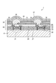
- FIG. 1 is a schematic cross-sectional view showing a configuration example of an electronic device according to an embodiment of the present invention.
- the resin film according to the embodiment of the present invention (hereinafter, abbreviated as "the resin film of the present invention” as appropriate) is a resin film containing polyimide and satisfies the conditions of the amount of charge change in the film shown below. Is. That is, the resin film of the present invention states that "the amount of charge change in the film when irradiated with light having a wavelength of 470 nm and an intensity of 4.0 ⁇ W / cm 2 for 30 minutes is 1.0 ⁇ 10 16 cm -3 or less". A resin film that satisfies the conditions.
- the amount of charge change in the film is the amount of charge change in the resin film when the light is irradiated for 30 minutes with respect to the amount of change in the charge before the irradiation of the light.
- Such an amount of charge change in the film is obtained by, for example, subtracting the amount of charge in the resin film before irradiation with the light from the amount of charge accumulated in the resin film when the light is irradiated for 30 minutes. , Can be calculated.
- the resin film of the present invention having the above structure is used as a substrate for a semiconductor element (for example, a flexible substrate), it is possible to suppress a change in the characteristics of the semiconductor element during long-term driving. Further, when the resin film of the present invention is provided on an electronic device as a substrate of a semiconductor element, the reliability of the electronic device can be improved. In particular, when the semiconductor element is a TFT and the electronic device is an organic EL display, the resin film of the present invention can suppress the shift of the threshold voltage of the TFT, thereby improving the reliability of the organic EL display. Can be made to.
- the reason why the resin film according to the embodiment of the present invention exerts the above effect is presumed as follows. That is, in a semiconductor element formed on a substrate, when an electric charge is present in the substrate, the carrier density in the semiconductor element changes due to the influence of the electric field caused by the electric charge, and the electrical characteristics of the semiconductor element change. For example, when a top gate type TFT is formed on a substrate, when an electric charge is present in the substrate, the substrate functions as a back gate, so that the threshold voltage of the TFT changes. If the amount of electric charge in the substrate changes while the semiconductor element is being driven, the electrical characteristics of the semiconductor element change with time, so that the reliability of the electronic device including the semiconductor element is impaired.
- the amount of electric charge in the polyimide film (hereinafter, appropriately referred to as the amount of electric charge in the film) changes as the semiconductor element on the polyimide film is driven. It is estimated to be.
- the mechanism by which the amount of charge in the film changes when a polyimide film is used is estimated as follows. That is, in most of the polyimides having high heat resistance, the highest occupied orbitals (HOMO) are unevenly distributed in the diamine moiety, and the lowest empty orbitals (LUMO) are unevenly distributed in the acid dianhydride moiety. Therefore, the electronic transition from HOMO to LUMO in the polyimide film is a charge transfer transition accompanied by a charge transfer from the diamine moiety to the acid dianhydride moiety. When a charge transfer transition occurs, a charge is generated in the polyimide film along with the charge transfer transition, and the generated charge is further trapped in the polyimide film. As a result, it is estimated that the amount of charge in the film changes.
- the blue light emitted from the organic EL display (specifically, the organic EL element) includes light having a wavelength of 470 nm. Therefore, in the organic EL display, the charge transfer transition of the polyimide occurs remarkably, and it is presumed that the amount of charge in the film of the substrate is likely to change as the organic EL display is driven.
- the resin film according to the embodiment of the present invention is a resin film containing polyimide, and "change in charge in the film when irradiated with light having a wavelength of 470 nm and an intensity of 4.0 ⁇ W / cm 2 for 30 minutes.
- the condition that the amount is 1.0 ⁇ 10 16 cm -3 or less ” is satisfied. That is, the resin film of the present invention is a resin film in which the amount of charge change in the film due to the above-mentioned external stress is small even if it contains polyimide.
- the resin film of the present invention when used as a substrate for a semiconductor element, the amount of charge change in the film due to the driving of the semiconductor element is small, and the change in the carrier amount of the semiconductor element can be suppressed. It is possible to obtain an electronic device having excellent reliability by suppressing the above.
- the amount of change in charge in the film in the present invention is a value obtained by the following method.
- a silicon wafer forming a semiconductor layer, a thermal oxide film, and a resin film containing polyimide (resin film to be measured) are laminated in this order.
- a resin film containing polyimide resin film to be measured
- a measurement sample is placed in a dark chamber of a capacitance-voltage characteristic (CV characteristic) measuring device, and the measurement sample is sandwiched between a pair of electrodes provided in the measuring device to form a capacitor structure containing the measurement sample.
- CV characteristic capacitance-voltage characteristic
- the resin film of the measurement sample constituting the capacitor structure is irradiated with light from the light source of the measuring device, whereby an electric charge due to photoexcitation is generated in the resin film.
- the electrode on the light source side is separated from the resin film of the measurement sample, and is brought into contact with the measurement sample again after light irradiation of the resin film.
- the wavelength of the light from this light source is 470 nm
- the intensity of the light is 4.0 ⁇ W / cm 2 .
- the irradiation time of the light is 30 minutes.
- the same DC bias voltage and AC voltage as described above are applied to the capacitor structure after light irradiation, and the charge due to voltage application and the charge due to photoexcitation are accumulated in the capacitor after light irradiation.
- Measure the capacitance of the structure and the applied voltage Based on the obtained measured values of capacitance and applied voltage, the CV characteristics of the capacitor structure after light irradiation are measured. Then, based on the measurement result of the CV characteristic, the flat band voltage V FB 2 of the capacitor structure after the light irradiation is derived.
- the flat band voltage difference ⁇ V FB is derived based on the following equation (F1). To do. Then, using the electrostatic capacitance C I of the obtained flat-band voltage difference [Delta] V FB and the charge storage state, based on the formula (F2) below, the amount of increase in charge due to light excitation per unit volume of the resin film, That is, the amount of change in charge Q [cm -3 ] in the resin film is derived.
- ⁇ V FB
- Q C I ⁇ ⁇ V FB / (qSt) ⁇ (F2)
- q is an elementary charge (1.6 ⁇ 10 -19 [C])
- S is the area of the electrode on the light source side [cm 2 ]
- t is the resin film to be measured.
- the resin film of the measurement sample in which the amount of charge change Q in the film obtained as described above is 1.0 ⁇ 10 16 cm -3 or less is adopted as the resin film in the present invention.
- the electrode on the light source side of the pair of electrodes is a mercury probe which is a movable electrode that is in contact with the resin film of the measurement sample so as to be separable.
- the resin film according to the embodiment of the present invention contains polyimide.
- This polyimide is preferably a resin having a repeating unit represented by the chemical formula (10).
- R 11 represents a tetravalent tetracarboxylic acid residue having 2 or more carbon atoms.
- R 12 represents a divalent diamine residue having 2 or more carbon atoms.
- R 11 is preferably a tetravalent hydrocarbon group having 2 to 80 carbon atoms.
- R 11 is a tetravalent organic group having 2 to 80 carbon atoms containing hydrogen and carbon as essential components and containing one or more atoms selected from boron, oxygen, sulfur, nitrogen, phosphorus, silicon and halogen. May be good.
- the number of each atom of boron, oxygen, sulfur, nitrogen, phosphorus, silicon and halogen contained in this organic group is preferably in the range of 20 or less, and more preferably in the range of 10 or less. ..
- the tetracarboxylic acid that gives R 11 is not particularly limited, and known ones can be used.
- this tetracarboxylic acid pyromellitic acid, 3,3', 4,4'-biphenyltetracarboxylic acid, 2,3,3', 4'-biphenyltetracarboxylic acid, 2,2', 3,3 '-Biphenyltetracarboxylic acid, 3,3', 4,4'-benzophenone tetracarboxylic acid, 2,2-bis (3,4-dicarboxyphenyl) hexafluoropropane, bis (3,4-dicarboxyphenyl) Sulfur, bis (3,4-dicarboxyphenyl) ether, cyclobutanetetracarboxylic acid, 1,2,3,4-cyclopentanetetracarboxylic acid, 1,2,4,5-cyclohexanetetracarboxylic acid, Examples thereof include the tetrac
- tetracarboxylic acids can be used as they are or in the form of acid anhydrides, active esters or active amides. Moreover, you may use 2 or more kinds of these as the tetracarboxylic acid which gives R 11.
- 50 mol% or more of 100 mol% of the tetracarboxylic acid residues contained in the polyimide consists of aromatic tetracarboxylic acid residues.
- 50 mol% or more of the tetracarboxylic acid residue is more preferably composed of at least one selected from the pyromellitic acid residue and the biphenyltetracarboxylic acid residue.
- 80 mol% or more of the 100 mol% of the tetracarboxylic acid residue is composed of at least one selected from the pyromellitic acid residue and the biphenyltetracarboxylic acid residue.
- the tetracarboxylic dians that give R 11 include dimethylsilanediphthalic acid and 1,3-bis (phthalic acid) in order to improve the applicability to the support and the resistance to oxygen plasma and UV ozone treatment used for cleaning.
- a silicon-containing tetracarboxylic acid such as tetramethyldisiloxane may be used. When these silicon-containing tetracarboxylic acids are used, it is preferable to use 1 to 30 mol% of the total tetracarboxylic acid.
- a part of hydrogen contained in the residue of the tetracarboxylic acid is a hydrocarbon group having 1 to 10 carbon atoms such as a methyl group and an ethyl group, and carbon such as a trifluoromethyl group. It may be substituted with a group of numbers 1 to 10, such as a fluoroalkyl group, F, Cl, Br, and I. Furthermore, if a part of the hydrogen contained in the residue is replaced with an acidic group such as OH, COOH, SO 3 H, CONH 2 , SO 2 NH 2 , the polyimide and its precursor are dissolved in an alkaline aqueous solution. Since the property is improved, it is preferable when it is used as a photosensitive resin composition described later.
- R 12 is preferably a divalent hydrocarbon group having 2 to 80 carbon atoms. Further, R 12 is a divalent organic group having 2 to 80 carbon atoms containing hydrogen and carbon as essential components and containing one or more atoms selected from boron, oxygen, sulfur, nitrogen, phosphorus, silicon and halogen. May be good.
- the number of each atom of boron, oxygen, sulfur, nitrogen, phosphorus, silicon and halogen contained in R 12 is preferably in the range of 20 or less, and more preferably in the range of 10 or less.
- the diamine that gives R 12 is not particularly limited, and known diamines can be used.
- this diamine m-phenylenediamine, p-phenylenediamine, 4,4'-diaminobenzanilide, 3,4'-diaminodiphenyl ether, 4,4'-diaminodiphenyl ether, 2,2'-dimethyl-4, 4'-diaminobiphenyl, 2,2'-di (trifluoromethyl) -4,4'-diaminobiphenyl, bis (4-aminophenoxyphenyl) sulfone, 1,4-bis (4-aminophenoxy) benzene, 1 , 3-bis (3-aminophenoxy) benzene, 1,3-bis (4-aminophenoxy) benzene, bis (3-amino-4-hydroxyphenyl) hexafluoropropane, ethylenediamine, propylene diamine, butanediamine,
- diamines can be used as-is or as the corresponding trimethylsilylated diamines. In addition, two or more of these may be used as the diamine that gives R 12.
- the polyimide is composed of aromatic diamine residues.
- 50 mol% or more of the diamine residue is composed of p-phenylenediamine residue.
- 80 mol% or more of the 100 mol% of the diamine residues is composed of p-phenylenediamine residues.
- the polyimide contained in the resin film of the present invention 50 mol% or more of 100 mol% of the tetracarboxylic acid residues contained in the polyimide is composed of pyromellitic acid residues and biphenyltetracarboxylic acid residues. It is composed of at least one selected, and 50 mol% or more of 100 mol% of the diamine residues contained in the polyimide is composed of p-phenylrangeamine residues.
- the value obtained by dividing the number of moles of the tetracarboxylic acid residue contained in the polyimide by the number of moles of the diamine residue contained in the polyimide is preferably 1.001 or more. More preferably, it is .005 or more.
- the division value Ka is preferably 1.100 or less, and more preferably 1.060 or less.
- the terminal structure of the polyimide tends to be an acid anhydride, and the amine terminal where the charge is easily trapped in the polyimide can be reduced. Therefore, it is possible to suppress a change in the amount of electric charge in the film of the resin film containing polyimide at the time of light irradiation.
- the division value Ka is 1.100 or less, the molecular weight of the polyimide is high, so that the terminal structure of the polyimide present in the resin film is reduced. Therefore, it is possible to suppress a change in the amount of electric charge in the film of the resin film containing polyimide at the time of light irradiation.
- the diamine that gives R 12 is 1,3-bis (3-aminopropyl) tetramethyldisiloxane in order to improve the coating property on the support and the resistance to oxygen plasma and UV ozone treatment used for cleaning.
- 1,3-Bis (4-anilino) Tetramethyldisiloxane or other silicon-containing diamines may be used.
- silicon-containing diamine compounds it is preferable to use 1 to 30 mol% of the total diamine compound.
- a part of hydrogen contained in the diamine compound has a hydrocarbon group having 1 to 10 carbon atoms such as a methyl group and an ethyl group, and 1 to 10 carbon atoms such as a trifluoromethyl group. It may be substituted with a group such as a fluoroalkyl group, F, Cl, Br, or I.
- an acidic group such as OH, COOH, SO 3 H, CONH 2 , SO 2 NH 2
- the polyimide and its precursor are dissolved in an aqueous alkaline solution. Since the property is improved, it is preferable when it is used as a photosensitive resin composition described later.
- the polyimide contained in the resin film of the present invention may have its end sealed with an end-sealing agent.
- the end of the polyimide is sealed, it is preferable that the polyimide contains at least one of a structure represented by the chemical formula (1) and a structure represented by the chemical formula (2).
- R 11 and R 12 are each the same as the R 11 and R 12 in the above-mentioned formula (10).
- R 13 represents a divalent dicarboxylic acid residue having 2 or more carbon atoms.
- R 11 represents a tetravalent tetracarboxylic acid residue having 2 or more carbon atoms.
- R 12 represents a divalent diamine residue having 2 or more carbon atoms.
- R 14 represents a monovalent monocarboxylic acid residue having 1 or more carbon atoms.
- R 13 is preferably a divalent hydrocarbon group having 2 to 80 carbon atoms. Further, R 13 is a divalent organic group having 2 to 80 carbon atoms containing hydrogen and carbon as essential components and containing one or more atoms selected from boron, oxygen, sulfur, nitrogen, phosphorus, silicon and halogen. May be good. The number of each atom of boron, oxygen, sulfur, nitrogen, phosphorus, silicon and halogen contained in R 13 is preferably in the range of 20 or less, and more preferably in the range of 10 or less.
- the dicarboxylic acid that gives R 13 is not particularly limited, but is preferably an aromatic dicarboxylic acid from the viewpoint of improving the heat resistance of the resin film.
- aromatic dicarboxylic acid examples include phthalic acid, 3,4-biphenyldicarboxylic acid, 2,3-biphenyldicarboxylic acid, 2,3-naphthalenedicarboxylic acid and the like.
- R 14 is preferably a monovalent hydrocarbon group having 1 to 80 carbon atoms. Further, R 14 is a monovalent organic group having 1 to 80 carbon atoms containing hydrogen and carbon as essential components and containing one or more atoms selected from boron, oxygen, sulfur, nitrogen, phosphorus, silicon and halogen. May be good. The number of each atom of boron, oxygen, sulfur, nitrogen, phosphorus, silicon and halogen contained in R 14 is preferably in the range of 20 or less, and more preferably in the range of 10 or less.
- the monocarboxylic acid that gives R 14 is not particularly limited, but is preferably an aromatic monocarboxylic acid from the viewpoint of improving the heat resistance of the resin film.
- aromatic monocarboxylic acid examples include benzoic acid, 2-biphenylcarboxylic acid, 3-biphenylcarboxylic acid, 4-biphenylcarboxylic acid, 1-naphthalenecarboxylic acid, 2-naphthalenecarboxylic acid and the like.
- the structure represented by the chemical formula (1) is a structure in which the amine terminal of polyimide is sealed with a dicarboxylic acid compound.
- the structure represented by the chemical formula (2) is a structure in which the amine terminal of polyimide is sealed with a monocarboxylic acid compound. Therefore, when the polyimide has these structures, the amine terminals of the polyimide present in the resin film are reduced, and therefore, the change in the amount of charge in the film during light irradiation in the resin film containing the polyimide can be suppressed. ..
- the resin having the structure represented by the chemical formula (1) (the resin of the chemical formula (1)) satisfies the following conditions. That is, the value obtained by dividing the number of moles of the tetracarboxylic acid residue contained in the resin of the chemical formula (1) by the number of moles of the diamine residue contained in the resin (division value Ka) is 1.001 or more. Is preferable, and more preferably 1.005 or more.
- the division value Ka is preferably 1.100 or less, and more preferably 1.060 or less.
- the terminal structure of the resin of the chemical formula (1) tends to be an acid anhydride, and the amine terminal in which charges are easily trapped in the resin can be reduced.
- the division value Ka is 1.100 or less, the molecular weight of the polyimide is high, so that the terminal structure of the polyimide present in the resin film is reduced. Therefore, it is possible to suppress a change in the amount of electric charge in the film of the resin film containing polyimide at the time of light irradiation.
- the resin having the structure represented by the chemical formula (2) (the resin of the chemical formula (2)) preferably satisfies the following conditions. That is, the division value Ka of the resin of the chemical formula (2) is preferably 1.001 or more, and more preferably 1.005 or more. The division value Ka is preferably 1.100 or less, and more preferably 1.060 or less. When the division value Ka is 1.001 or more, the terminal structure of the resin of the chemical formula (2) tends to be an acid anhydride, and the amine terminal in which charges are easily trapped in the resin can be reduced. Therefore, it is possible to suppress a change in the amount of electric charge in the film of the resin film containing polyimide at the time of light irradiation.
- the division value Ka is 1.100 or less, the molecular weight of the polyimide is high, so that the terminal structure of the polyimide present in the resin film is reduced. Therefore, it is possible to suppress a change in the amount of electric charge in the film of the resin film containing polyimide at the time of light irradiation.
- the resin film according to the embodiment of the present invention can be obtained by applying a resin composition containing polyimide or a precursor thereof and a solvent to a support and firing it.
- the polyimide precursor refers to a resin that can be converted into polyimide by heat treatment, chemical treatment, or the like.
- a polyimide precursor that can be preferably used in the present invention is a polyamic acid.
- the polyamic acid is preferably a resin having a repeating unit represented by the chemical formula (11).
- R 1 and R 2 represent a hydrogen atom, an alkali metal ion, an ammonium ion, an imidazolium ion, a hydrocarbon group having 1 to 10 carbon atoms or an alkylsilyl group having 1 to 10 carbon atoms.
- R 11 and R 12 are each the same as the R 11 and R 12 in the above-mentioned formula (10).
- Specific examples of R 11 in the chemical formula (11) include the structures described as specific examples of R 11 in the above-mentioned chemical formula (10).
- Specific examples of R 12 in the chemical formula (11) include the structures described as specific examples of R 12 in the above-mentioned chemical formula (10).
- the polyimide precursor may be end-sealed with an end-capping agent.
- the molecular weight of the polyimide precursor can be adjusted to a preferable range.
- terminal monomer of the polyimide precursor is a diamine compound, dicarboxylic acid anhydride, monocarboxylic acid, monocarboxylic acid chloride compound, monocarboxylic acid active ester compound, in order to seal the amino group of this diamine compound, A dicarbonate dialkyl ester or the like can be used as the terminal encapsulant.
- the monomer at the end of the polyimide precursor is an acid dianhydride, monoamine, monoalcohol, or the like may be used as the terminal sealant in order to seal the acid anhydride group of the acid dianhydride. it can.
- the polyimide precursor has an amine terminal sealed, it is preferable that the polyimide precursor has a structure represented by the chemical formula (3).
- R 11 and R 12 are each the same as the R 11 and R 12 in the above-mentioned formula (10).
- R 15 shows the terminal structure of the resin, and specifically, shows the structure represented by the chemical formula (4).
- R 1 and R 2 independently represent a hydrogen atom, a hydrocarbon group having 1 to 10 carbon atoms, an alkylsilyl group having 1 to 10 carbon atoms, an alkali metal ion, an ammonium ion, an imidazolium ion or a pyridinium ion, respectively. ..
- ⁇ represents a monovalent hydrocarbon group having 2 or more carbon atoms.
- ⁇ is preferably a monovalent hydrocarbon group having 2 to 10 carbon atoms. More preferably, ⁇ is an aliphatic hydrocarbon group.
- the aliphatic hydrocarbon group may be linear, branched or cyclic.
- ⁇ and ⁇ independently represent an oxygen atom or a sulfur atom, respectively. Preferred as ⁇ and ⁇ are oxygen atoms.
- hydrocarbon group examples include an ethyl group, an n-propyl group, an n-butyl group, an n-pentyl group, an n-hexyl group, an n-heptyl group, an n-octyl group, an n-nonyl group and n.
- -Linear hydrocarbon groups such as decyl groups, isopropyl groups, isobutyl groups, sec-butyl groups, tert-butyl groups, isopentyl groups, sec-pentyl groups, tert-pentyl groups, isohexyl groups, sec-hexyl groups, etc.
- cyclic hydrocarbon groups such as a branched chain hydrocarbon group, a cyclopropyl group, a cyclobutyl group, a cyclopentyl group, a cyclohexyl group, a cycloheptyl group, a cyclooctyl group, a norbornyl group and an adamantyl group.
- hydrocarbon groups a monovalent branched chain hydrocarbon group having 2 to 10 carbon atoms and a cyclic hydrocarbon group are preferable, and an isopropyl group, a cyclohexyl group, a tert-butyl group and a tert-pentyl group are more preferable.
- the tert-butyl group is most preferred.
- R 15 When a resin having a structure represented by the chemical formula (3) is heated, R 15 is thermally decomposed to generate an amino group at the end of the resin.
- the amino group generated at the terminal can react with another resin having a tetracarboxylic acid at the terminal. Therefore, the resin obtained by heating the resin having the structure represented by the chemical formula (3) has a high molecular weight and a small terminal structure.
- a resin film containing such a resin specifically, polyimide
- the resin having the structure represented by the chemical formula (3) preferably satisfies the following conditions. That is, the value obtained by dividing the number of moles of the tetracarboxylic acid residue contained in the resin by the number of moles of the diamine residue contained in the resin (division value Kb) is more preferably 1.001 or more. It is more preferably 1.005 or more. Further, the division value Kb is more preferably 1.100 or less, and further preferably 1.060 or less.
- the R 15 at the time of heating of the resin is substantially all amino groups generated by thermal decomposition, to react with an acid anhydride group present at the end of the other resins
- the resin (specifically, polyimide) obtained by heating has an extremely high molecular weight and has a particularly small amount of amine terminals. Therefore, it is possible to suitably suppress the change in the amount of electric charge in the film of the resin film containing polyimide during light irradiation.
- the division value Kb is 1.100 or less, the molecular weight of the resin (specifically, polyimide) obtained by heating is high, so that the terminal structure of the polyimide present in the resin film is reduced. Therefore, it is possible to suppress a change in the amount of electric charge in the film of the resin film containing polyimide at the time of light irradiation.
- the polyimide precursor has an amine terminal sealed, it is also preferable that the polyimide precursor has a structure represented by the chemical formula (5).
- R 11 and R 12 are each the same as the R 11 and R 12 in the above-mentioned formula (10).
- R 16 shows the terminal structure of the resin, and specifically, shows the structure represented by the chemical formula (6) or the structure represented by the chemical formula (7).
- R 13 represents a divalent dicarboxylic acid residue having 2 or more carbon atoms.
- R 14 represents a monovalent monocarboxylic acid residue having 1 or more carbon atoms.
- R 16 in the chemical formula (5) has a structure represented by the chemical formula (6)
- it is represented by the above-mentioned chemical formula (1) by heating a resin having the structure represented by the chemical formula (5).
- a resin having a structure can be obtained.
- R 16 in the chemical formula (5) has a structure represented by the chemical formula (7)
- it is represented by the above-mentioned chemical formula (2) by heating a resin having the structure represented by the chemical formula (5).
- a resin having a structure can be obtained.
- the solvent contained in the above resin composition can be used without particular limitation as long as it dissolves polyimide and its precursor.
- solvents include, for example, N-methyl-2-pyrrolidone, ⁇ -butyrolactone, N, N-dimethylformamide, N, N-dimethylacetamide, 3-methoxy-N, N-dimethylpropionamide, 3-butoxy-.
- Aprotonic polar solvents such as N, N-dimethylpropionamide, N, N-dimethylisobutylamide, 1,3-dimethyl-2-imidazolidinone, N, N'-dimethylpropylene urea, dimethylsulfoxide, tetrahydrofuran, dioxane , Ethylene glycol monomethyl ether, propylene glycol monoethyl ether, diethylene glycol monomethyl ether, diethylene glycol monoethyl ether, diethylene glycol ethyl methyl ether, diethylene glycol dimethyl ether and other ethers, acetone, methyl ethyl ketone, diisobutyl ketone, diacetone alcohol, cyclohexanone and other ketones, Ethyl acetate, propylene glycol monomethyl ether acetate, ethyl lactate, 3-methyl-3-methoxybutyl acetate, ethylene glycol ethyl
- Polyimide or its precursor can be polymerized by known methods.
- a reaction solvent contains tetracarboxylic acid or the corresponding acid dianhydride, active ester, active amide or the like as an acid component, and diamine or the corresponding trimethylsilylated diamine as a diamine component.
- Polyamic acid can be obtained by polymerizing in.
- the carboxy group forms a salt with an alkali metal ion, an ammonium ion, and an imidazolium ion, or is esterified with a hydrocarbon group having 1 to 10 carbon atoms or an alkylsilyl group having 1 to 10 carbon atoms. It may be the one.
- the terminal encapsulant When producing a polyimide having a sealed end or a precursor thereof, the terminal encapsulant may be reacted with a monomer before polymerization or with a polyimide during or after polymerization or a precursor thereof.
- the desired polyimide or a precursor thereof can be obtained.
- a resin having a structure represented by the above-mentioned chemical formula (3) or chemical formula (5) as a polyimide having a sealed end or a precursor thereof can be produced by the following two methods.
- the first production method is a method for producing a resin having a structure represented by the chemical formula (3) or the chemical formula (5) by a two-step method shown below. Specifically, in this production method, in the first step, the diamine compound is reacted with the terminal amino group encapsulant to produce the compound represented by the chemical formula (41) or the chemical formula (51).
- the terminal amino group encapsulant is an example of an end encapsulant for encapsulating the end of polyimide or a precursor thereof, and specifically, it reacts with an amino group of a diamine compound and has a chemical formula. (41) or a compound that produces a compound represented by the chemical formula (51).
- the compound represented by the chemical formula (41) or the chemical formula (51) is reacted with the diamine compound and the tetracarboxylic dian to form a structure represented by the chemical formula (3) or the chemical formula (5).
- R 12 represents a divalent diamine residue having 2 or more carbon atoms.
- R 15 represents a structure represented by the chemical formula (4).
- R 12 represents a divalent diamine residue having 2 or more carbon atoms.
- R 16 represents a structure represented by the chemical formula (6) or a structure represented by the chemical formula (7).
- the second production method is a method for producing a resin having a structure represented by the chemical formula (3) or the chemical formula (5) by a two-step method shown below. Specifically, in this production method, in the first step, the diamine compound and the tetracarboxylic acid are reacted to produce a resin having a structure represented by the chemical formula (42). In the subsequent second step, the resin having the structure represented by the chemical formula (42) is reacted with the terminal amino group encapsulant described above, and the resin having the structure represented by the chemical formula (3) or the chemical formula (5) is reacted. To manufacture.
- R 11 and R 12 are each the same as the R 11 and R 12 in the above-mentioned formula (10).
- R 1 and R 2 independently represent a hydrogen atom, a hydrocarbon group having 1 to 10 carbon atoms, an alkylsilyl group having 1 to 10 carbon atoms, an alkali metal ion, an ammonium ion, an imidazolium ion or a pyridinium ion, respectively. ..
- the solvent described as a specific example of the solvent contained in the resin composition can be used alone or in combination of two or more.
- the amount of the above reaction solvent used is preferably adjusted so that the total amount of the tetracarboxylic acid and the diamine compound is 0.1 to 50% by mass of the total amount of the reaction solution.
- the reaction temperature is preferably ⁇ 20 ° C. to 150 ° C., more preferably 0 ° C. to 100 ° C. Further, the reaction time is preferably 0.1 to 24 hours, more preferably 0.5 to 12 hours.
- the polyamic acid solution obtained as the polyimide precursor may be used as it is as a resin composition.
- the desired resin composition can be obtained without isolating the resin by using the same solvent as the one used as the resin composition as the reaction solvent or by adding the solvent after the reaction is completed.
- the polyamic acid obtained as described above may be further imidized or esterified as a part of the repeating unit of the polyamic acid.
- the polyamic acid solution obtained by polymerizing the polyamic acid may be used as it is in the reaction, or the polyamic acid may be isolated and then used in the reaction.
- the resin composition preferably contains at least one of a compound having a structure represented by the chemical formula (8) and a compound having a structure represented by the chemical formula (9). These compounds react with the amine ends of the polyamic acid during calcination of the polyamic acid. Therefore, by firing the resin composition containing at least one of these compounds, the resin having the structure represented by the above-mentioned chemical formula (1) or chemical formula (2) without lowering the molecular weight of the polyamic acid. (Specifically, polyimide) can be obtained.
- R 13 represents a divalent dicarboxylic acid residue having 2 or more carbon atoms.
- R 3 and R 4 independently represent a hydrogen atom, a hydrocarbon group having 1 to 10 carbon atoms, an alkylsilyl group having 1 to 10 carbon atoms, an alkali metal ion, an ammonium ion, an imidazolium ion or a pyridinium ion, respectively. ..
- Specific examples of R 13 include the structures described as specific examples of R 13 in the above-mentioned formula (1).
- R 14 represents a monovalent monocarboxylic acid residue having 1 or more carbon atoms.
- R 5 represents a hydrogen atom, a hydrocarbon group having 1 to 10 carbon atoms, an alkylsilyl group having 1 to 10 carbon atoms, an alkali metal ion, an ammonium ion, an imidazolium ion or a pyridinium ion.
- R 14 include the structures described as specific examples of R 14 in the above-mentioned formula (2).
- the content of at least one of the compound having the structure represented by the chemical formula (8) and the compound having the structure represented by the chemical formula (9) in the resin composition is 100% by mass of the polyimide precursor in the resin composition. It is preferably 0.05 parts by mass or more, and more preferably 0.1 parts by mass or more. The content is preferably 5.0 parts by mass or less, and more preferably 3.0 parts by mass or less, based on 100 parts by mass of the polyimide precursor in the resin composition.
- the content is 0.05 parts by mass or more, the amine terminal of the polyamic acid can be reduced, so that the change in the amount of charge in the film of the resin film containing polyimide can be suppressed during light irradiation.
- the content is 5.0% by mass or less, it is possible to suppress the decrease in heat resistance of the resin film due to the residual component that did not react with the amine terminal.
- the resin composition may contain a photoacid generator (a), a heat-crosslinking agent (b), a heat acid generator (c), a compound containing a phenolic hydroxyl group (d), and an adhesion improver (adhesion improving agent), if necessary. It may contain at least one additive selected from e) and the surfactant (f). Specific examples of these additives include those described in International Publication No. 2017/099183.
- the resin composition can be made into a photosensitive resin composition by containing the photoacid generator (a).
- the photoacid generator (a) acid is generated in the light-irradiated portion of the resin composition, the solubility of the light-irradiated portion in the alkaline aqueous solution is increased, and the light-irradiated portion is dissolved. Relief pattern can be obtained.
- the photoacid generator (a) and the epoxy compound or the heat-crosslinking agent (b) described later the acid generated in the light-irradiated portion causes the cross-linking reaction of the epoxy compound and the heat-crosslinking agent (b). It is possible to obtain a negative-type relief pattern that promotes and insolubilizes the light-irradiated portion.
- Examples of the photoacid generator (a) include quinonediazide compounds, sulfonium salts, phosphonium salts, diazonium salts, iodonium salts and the like.
- the resin composition may contain two or more of these, whereby a highly sensitive photosensitive resin composition can be obtained.
- the resin composition can enhance the chemical resistance and hardness of the resin film obtained by heating.
- the content of the thermal cross-linking agent (b) is preferably 10 parts by mass or more and 100 parts by mass or less with respect to 100 parts by mass of the resin composition.
- the content of the thermal cross-linking agent (b) is 10 parts by mass or more and 100 parts by mass or less, the strength of the obtained resin film is high and the storage stability of the resin composition is also excellent.
- the resin composition may further contain the thermal acid generator (c).
- the thermal acid generator (c) generates an acid by heating after development, which will be described later, and promotes a cross-linking reaction between polyimide or its precursor and the heat-crosslinking agent (b), and also promotes a curing reaction. Therefore, the chemical resistance of the obtained heat-resistant resin film (specifically, the resin film containing polyimide) is improved, and the film loss can be reduced.
- the acid generated from the thermoacid generator (c) is preferably a strong acid, for example, aryl sulfonic acid such as p-toluene sulfonic acid and benzene sulfonic acid, methane sulfonic acid, ethane sulfonic acid, butane sulfonic acid and the like. Alkyl sulfonic acid and the like are preferable.
- the content of the thermal acid generator (c) is preferably 0.5 parts by mass or more and 10 parts by mass or less with respect to 100 parts by mass of the resin composition from the viewpoint of further promoting the crosslinking reaction. It is preferable to have.
- the resin composition may contain a compound (d) containing a phenolic hydroxyl group for the purpose of supplementing the alkali developability of the photosensitive resin composition.
- the photosensitive resin composition obtained by containing the compound (d) containing a phenolic hydroxyl group hardly dissolves in an alkaline developer before exposure, and easily dissolves in an alkaline developer when exposed. Development can be easily performed in a short time with little film loss. Therefore, the sensitivity is likely to be improved.
- the content of the compound (d) containing such a phenolic hydroxyl group is preferably 3 parts by mass or more and 40 parts by mass or less with respect to 100 parts by mass of the resin composition.
- the resin composition may contain an adhesion improver (e).
- an adhesion improver e
- the adhesion improver (e) when developing a photosensitive resin composition, the adhesion between a base material such as a silicon wafer, ITO, SiO 2 , or silicon nitride and the photosensitive resin composition can be improved. Can be enhanced.
- the adhesion between the photosensitive resin composition and the underlying substrate it is possible to increase the resistance of the photosensitive resin composition to oxygen plasma and UV ozone treatment used for cleaning and the like.
- the content of the adhesion improver (e) is preferably 0.005 parts by mass or more and 10 parts by mass or less with respect to 100 parts by mass of the resin composition.
- the resin composition may contain a surfactant (f) in order to improve the coatability.
- a surfactant (f) examples include "Florard” (registered trademark) manufactured by Sumitomo 3M, "Megafuck” (registered trademark) manufactured by DIC, and “Sulflon” (registered trademark) manufactured by Asahi Glass Co., Ltd. Fluorosurfactants, KP341 manufactured by Shinetsu Chemical Industry Co., Ltd., DBE manufactured by Chisso Co., Ltd., "Polyflow” (registered trademark), “Glanol” (registered trademark) manufactured by Kyoeisha Chemical Co., Ltd., BYK manufactured by Big Chemie, etc.
- the content of the surfactant (f) is preferably 0.01 parts by mass or more and 10 parts by mass or less with respect to 100 parts by mass of the resin composition.
- the method for dissolving the additive in the resin composition include stirring and heating.
- the heating temperature is preferably set within a range that does not impair the performance of the photosensitive resin composition, and is usually room temperature to 80 ° C.
- the dissolution order of each component is not particularly limited, and for example, there is a method of sequentially dissolving compounds having low solubility.
- a component such as a surfactant (f) that easily generates bubbles during stirring and dissolution
- a surfactant (f) that easily generates bubbles during stirring and dissolution
- the varnish which is an example of the resin composition obtained by the above-mentioned production method, is preferably filtered using a filter to remove foreign substances such as dust.
- the pore size of this filter includes, but is not limited to, for example, 10 ⁇ m, 3 ⁇ m, 1 ⁇ m, 0.5 ⁇ m, 0.2 ⁇ m, 0.1 ⁇ m, 0.07 ⁇ m, 0.05 ⁇ m, and the like.
- the material of this filter includes polypropylene (PP), polyethylene (PE), nylon (NY), polytetrafluoroethylene (PTFE) and the like, but polyethylene and nylon are preferable.
- This method for producing a resin film is an example of a method for producing a resin film according to an embodiment of the present invention from the above-mentioned resin composition.
- the method for producing this resin film includes a coating step of applying a resin composition containing polyimide or a polyimide precursor and a solvent to a support, and a coating step of heating the coating film obtained by this coating step to heat the resin film. Including a heating step to obtain.
- varnish which is one of the resin compositions in the present invention
- the support include wafer substrates such as silicon and gallium arsenic, glass substrates such as sapphire glass, soda lime glass, and non-alkali glass, metal substrates such as stainless steel and copper, metal foils, and ceramic substrates.
- wafer substrates such as silicon and gallium arsenic
- glass substrates such as sapphire glass, soda lime glass, and non-alkali glass
- metal substrates such as stainless steel and copper, metal foils, and ceramic substrates.
- non-alkali glass is preferable from the viewpoint of surface smoothness and dimensional stability during heating.
- Examples of the varnish coating method include a spin coating method, a slit coating method, a dip coating method, a spray coating method, a printing method, and the like, and these may be combined.
- a display substrate for example, a substrate for a semiconductor element such as a TFT provided on a display
- the slit coating method is particularly preferably used.
- the support may be pretreated prior to application.
- the pretreatment agent is added to a solvent such as isopropanol, ethanol, methanol, water, tetrahydrofuran, propylene glycol monomethyl ether acetate, propylene glycol monomethyl ether, ethyl lactate, and diethyl adipate for 0.5 to 20.
- a solvent such as isopropanol, ethanol, methanol, water, tetrahydrofuran, propylene glycol monomethyl ether acetate, propylene glycol monomethyl ether, ethyl lactate, and diethyl adipate for 0.5 to 20.
- a method of treating the surface of the support by a method such as spin coating, slit die coating, bar coating, dip coating, spray coating, and steam treatment using a solution dissolved in mass%.
- a vacuum drying treatment can be performed, and then the reaction between the support and the pretreatment agent can be allowed to proceed by heat treatment at
- a drying method vacuum drying, heat drying, or a combination thereof can be used.
- a method of vacuum drying for example, a support in which a coating film is formed is placed in a vacuum chamber, and the coating film is dried by reducing the pressure in the vacuum chamber.
- a method of heat drying a method of drying the coating film using a hot plate, an oven, infrared rays or the like can be mentioned.
- a hot plate the support on which the coating film is formed is held and the coating film is heated and dried directly on the plate or on a jig such as a proxy pin installed on the plate.
- the heating temperature varies depending on the type and purpose of the solvent used for the varnish, and it is preferable to heat the varnish in the range of room temperature to 180 ° C. for 1 minute to several hours.
- a pattern can be formed from the dried coating film by the method described below.
- chemical rays are irradiated and exposed through a mask having a desired pattern on the coating film.
- Chemical rays used for exposure include ultraviolet rays, visible rays, electron beams, X-rays, etc., but in the present invention, i-rays (365 nm), h-rays (405 nm), and g-rays (436 nm) of mercury lamps can be used. preferable.
- the coating film has positive photosensitivity, the exposed portion of the coating film dissolves in the developer.
- the coating film has a negative photosensitive property, the exposed portion of the coating film is cured and insolubilized in a developing solution.
- a developing solution is used to remove the exposed part in the case of the positive type and the non-exposed part in the case of the negative type to form a desired pattern on the coating film.
- an aqueous solution of an alkaline compound such as tetramethylammonium is preferable in both the positive type and the negative type.
- a polar solvent such as N-methyl-2-pyrrolidone, alcohols, esters, ketones and the like may be added alone or in combination of a plurality of kinds to these alkaline aqueous solutions.
- a heating process is performed in which the coating film on the support is heat-treated to produce a resin film.
- the coating film is heat-treated in the range of 180 ° C. or higher and 600 ° C. or lower, preferably 220 ° C. or higher and 600 ° C. or lower, and more preferably 420 ° C. or higher and 490 ° C. or lower, and the coating film is fired.
- the heating temperature (calcination temperature) of the coating film in the heating step is 220 ° C. or higher, imidization proceeds sufficiently and a resin film having excellent mechanical properties can be obtained.
- the heating temperature is 420 ° C.
- a resin film having excellent heat resistance can be obtained.
- the heating temperature is 490 ° C. or lower, a resin film in which the charge transfer transition is unlikely to occur can be obtained. Therefore, when the heating temperature is 420 ° C. or higher and 490 ° C. or lower, changes in the amount of electric charge in the film during light irradiation in a resin film having excellent mechanical properties and heat resistance such as a resin film containing polyimide can be more easily suppressed. can do.
- the resin film obtained through the above coating step and heating step can be used by peeling from the support, or can be used as it is without peeling from the support.
- Examples of the peeling method include a mechanical peeling method, a method of immersing in water, a method of immersing in a chemical solution such as hydrochloric acid or hydrofluoric acid, and a laser beam in the wavelength range from ultraviolet light to infrared light with a resin film and a support.
- a method of irradiating the interface of the above can be mentioned.
- peeling using an ultraviolet laser is preferable.
- a mold release agent may be applied to the support or a sacrificial layer may be formed before the resin composition is applied to the support.
- Examples of the release agent include silicone-based, fluorine-based, aromatic polymer-based, and alkoxysilane-based.
- Examples of the sacrificial layer include a metal film, a metal oxide film, an amorphous silicon film, and the like.
- the film thickness of the resin film according to the embodiment of the present invention is not particularly limited, but is preferably 4 ⁇ m or more, more preferably 5 ⁇ m or more, and further preferably 6 ⁇ m or more.
- the film thickness of the resin film is preferably 40 ⁇ m or less, more preferably 30 ⁇ m or less, and even more preferably 25 ⁇ m or less.
- the film thickness of the resin film is 4 ⁇ m or more, sufficient mechanical properties can be obtained as a substrate for a semiconductor element.
- the film thickness of the resin film is 40 ⁇ m or less, sufficient toughness can be obtained as a substrate for a semiconductor element.
- the 0.05% weight loss temperature is not particularly limited, but is preferably 490 ° C. or higher, more preferably 495 ° C. or higher. ..
- the 0.05% weight loss temperature of the resin film is 490 ° C. or higher, it is possible to suppress the film floating phenomenon in which the inorganic film formed on the resin film floats from the film surface due to the high temperature process of device manufacturing. ..
- the light transmittance at a wavelength of 470 nm when the film thickness is converted to 10 ⁇ m is not particularly limited, but is preferably 60% or more. , 65% or more is more preferable.
- the light transmittance is 60% or more, photoexcitation of the resin film is unlikely to occur, so that the change in the amount of charge in the film during light irradiation in the resin film can be more easily suppressed.
- FIG. 1 is a schematic cross-sectional view showing a configuration example of an electronic device according to an embodiment of the present invention.
- the electronic device 1 includes a resin film 10 and a semiconductor element 21 formed on the resin film 10. Further, in the case of an image display device, for example, the electronic device 1 further includes image display elements 31 to 33.
- the resin film 10 is the resin film according to the embodiment of the present invention, and functions as a substrate (for example, a flexible substrate) of the electronic device 1 as shown in FIG.
- a semiconductor element 21 is formed on the resin film 10.
- the semiconductor element 21 is, for example, a thin film transistor (TFT), and includes a semiconductor layer 22, a gate insulating film 23, a gate electrode 24, a drain electrode 25, and a source electrode 26, as shown in FIG.
- the semiconductor layer 22 is provided between the drain electrode 25 and the source electrode 26.
- the gate insulating film 23 electrically insulates the semiconductor layer 22 and the gate electrode 24.
- the electronic device 1 includes an element layer 20 including a plurality of semiconductor elements 21 and interlayer insulating films 27 and 28 on the resin film 10.
- the electronic device 1 includes a light emitting layer 30 on the element layer 20.
- the light emitting layer 30 includes a plurality of image display elements 31 to 33, a pixel electrode 34, a partition wall 35, a counter electrode 36, and a sealing film 37.
- Each of the image display elements 31 to 33 is an element that emits light of a color necessary for displaying an image.
- the image display elements 31 to 33 are organic EL elements that emit red light, green light, and blue light, respectively.
- Each of these image display elements 31 to 33 is electrically connected to the source electrode 26 of the semiconductor element 21 via the pixel electrode 34.
- the pixel electrode 34 in the light emitting layer 30 is electrically insulated from the drain electrode 25 in the element layer 20 by the interlayer insulating film 28. Further, a partition wall 35 is provided between each of the image display elements 31 to 33. A counter electrode 36 is formed on the image display elements 31 to 33 and the partition wall 35. The sealing film 37 is formed on the counter electrode 36 and protects the image display elements 31 to 35 and the like.
- FIG. 1 illustrates an electronic device 1 that functions as an image display device, but the present invention is not limited thereto.
- the electronic device 1 may be a device other than an image display device such as a touch panel.
- the electronic device 1 may include a component other than the light emitting layer 30 such as a touch panel unit on the element layer 20.
- the semiconductor element 21 included in the electronic device 1 is not limited to the TFT shown in FIG. 1, and may be either a top gate type or bottom gate type TFT, or may be a semiconductor element other than the TFT. ..
- the number of semiconductor elements and image display elements arranged in the electronic device 1 is not particularly limited.
- the above-mentioned resin film is manufactured on a support such as a glass substrate by performing a coating step, a heating step, and the like according to the above-mentioned resin film manufacturing method.
- the resin film produced in this way can be used as a substrate for a semiconductor element in an electronic device (hereinafter, appropriately referred to as an element substrate) regardless of whether it is formed on the support or peeled off from the support. Can be used.
- an inorganic film is provided on the resin film as needed. This makes it possible to prevent moisture and oxygen from passing through the resin film from the outside of the substrate and causing deterioration of the pixel driving element and the light emitting element.
- the inorganic film examples include silicon oxide (SiOx), silicon nitride (SiNy), and silicon oxynitride (SiOxNy). These can be used to form a single layer, or can be used to form a plurality of layers by stacking a plurality of types. Further, these inorganic films can also be used by alternately laminating them with an organic film such as polyvinyl alcohol.
- the method for forming these inorganic films is preferably performed by using a vapor deposition method such as a chemical vapor deposition method (CVD) or a physical vapor deposition method (PVD).
- CVD chemical vapor deposition method
- PVD physical vapor deposition method
- the resin film by forming a resin film on the inorganic film or further forming the inorganic film as needed, it is possible to manufacture an element substrate having a plurality of layers of the inorganic film and the resin film. From the viewpoint of simplifying the process, it is preferable that the resin compositions used in the production of each resin film are the same resin composition.
- the semiconductor element is formed on the resin film obtained as described above.
- a TFT such as a top gate type TFT or a bottom gate type TFT is formed on the resin film.
- a TFT such as a top gate type TFT or a bottom gate type TFT is formed on the resin film.
- a semiconductor layer 22, a gate insulating film 23, and a gate electrode 24 are formed on the resin film 10 so as to cover them.
- An interlayer insulating film 27 is formed on the surface.
- a contact hole is formed in the interlayer insulating film 27, and the contact hole is embedded to form a pair of drain electrodes 25 and a source electrode 26.
- an interlayer insulating film 28 is formed so as to cover them.
- the semiconductor layer includes a channel region (active layer) in a region facing the gate electrode.
- the semiconductor layer may be composed of low-temperature polycrystalline silicon (LTPS), non-crystalline silicon (a-Si), or the like, and may be composed of indium tin oxide (ITZO), indium tin oxide zinc (IGZO: InGaZnO), zinc oxide ( It may be composed of oxide semiconductors such as ZnO), indium zinc oxide (IZO), indium gallium oxide (IGO), indium tin oxide (ITO) and indium oxide (InO).
- LTPS low-temperature polycrystalline silicon
- a-Si non-crystalline silicon
- ITZO indium tin oxide zinc
- ZnO zinc oxide
- IZO indium zinc oxide
- IGO indium gallium oxide
- ITO indium tin oxide
- InO indium oxide
- LTPS when forming LTPS, after a-Si formation, annealing at 450 ° C. for 120 minutes or the like for the purpose of dehydrogenation may be performed.
- annealing at 450 ° C. for 120 minutes or the like for the purpose of dehydrogenation may be performed.
- the heat resistance of the resin film is insufficient, the inorganic film on the resin film may float, the semiconductor layer may be destroyed, and the TFT may be damaged.
- the gate insulating film (gate insulating film 23 and the like illustrated in FIG. 1) is made of, for example, one of silicon oxide (SiOx), silicon nitride (SiNx), silicon oxynitride (SiON), aluminum oxide (AlOx), and the like. It is preferable that the monolayer film is composed of a single-layer film or a laminated film composed of two or more of them.
- the gate electrode controls the carrier density in the semiconductor layer by the applied gate voltage and also has a function as a wiring for supplying an electric potential.
- the constituent materials of the gate electrode include titanium (Ti), tungsten (W), tantalum (Ta), aluminum (Al), molybdenum (Mo), silver (Ag), neodymium (Nd), and copper (Cu). Examples include singles and alloys, including at least one of them.
- the constituent material of the gate electrode may be a compound containing at least one of them, and a laminated film containing two or more of them. Further, as a constituent material of the gate electrode, for example, a transparent conductive film such as ITO may be used.
- the interlayer insulating film (interlayer insulating films 27, 28, etc. illustrated in FIG. 1) is made of, for example, an organic material such as an acrylic resin, a polyimide (PI), or a novolak resin.
- an inorganic material such as a silicon oxide film, a silicon nitride film, a silicon oxynitride film, and aluminum oxide may be used as the interlayer insulating film.
- the source electrode and the drain electrode each function as a source or drain in the TFT.
- the source electrode and the drain electrode are configured to include, for example, a metal or a transparent conductive film similar to those listed as the constituent materials of the gate electrode described above. As these source electrodes and drain electrodes, it is desirable to select a material having good electrical conductivity.
- the TFT obtained as an example of a semiconductor element can be used in an image display device such as an organic EL display, a liquid crystal display, an electronic paper, or a ⁇ LED display.
- the electronic device in the present invention is an organic EL display
- the image display element used for the organic EL display is formed on the TFT by the following procedure. That is, a pixel electrode, an organic EL element, a counter electrode, and a sealing film are formed on the TFT in this order.
- the pixel electrode is connected to, for example, the source electrode and the drain electrode described above.
- the counter electrode is configured so that a common cathode potential is supplied to each pixel through, for example, wiring.
- the sealing film (sealing film 37 or the like illustrated in FIG.
- the sealing film may be made of, for example, an inorganic material such as silicon oxide (SiOx), silicon nitride (SiNx), silicon nitriding (SiON), or other organic material.
- the resin film on which the semiconductor element is formed is peeled from the support as described above, and an electronic device provided with this resin film is manufactured.
- Examples of the method of peeling the support and the resin film at these interfaces include a method using a laser, a mechanical peeling method, and a method of etching the support.
- the support such as a glass substrate is irradiated with the laser from the side where the semiconductor element is not formed, so that the support and the resin film are peeled off without damaging the semiconductor element. be able to.
- a primer layer for facilitating the peeling of the support and the resin film may be provided between the support and the resin film.
- laser light in the wavelength range from ultraviolet light to infrared light can be used, but ultraviolet light is particularly preferable.
- a more preferred laser beam is an excimer laser at 308 nm. Peeling energy in peeling the support and the resin film is preferably 250 mJ / cm 2 or less, and more preferably 200 mJ / cm 2 or less.
- First item amount of change in charge in the resin film
- the measurement of the amount of charge change in the resin film will be described.
- a laminate of a resin film and a Si wafer with a thermal oxide film is prepared for each resin film obtained in each example, and the amount of charge change in the film is measured for the prepared laminate by the following procedure. Carried out.
- the above-mentioned laminate as a measurement sample is placed on an electrode serving as a measurement stage in a dark room so that the Si wafer side is in contact with each other, and the electrode area is 0.026 cm 2 on the resin film of the placed laminate.
- the mercury probe of No. 1 was brought into contact with each other to form a capacitor structure containing the resin film.
- a DC bias voltage and an AC voltage are applied to the capacitor structure to measure the CV characteristics of the capacitor structure, and based on the measurement results of the CV characteristics, the flat band voltage V of the capacitor structure is measured.
- FB 1 was determined and [V] and the capacitance C I [F] of the charge accumulation state.
- the measurement conditions for this CV characteristic were an AC frequency of 100 kHz and a DC bias voltage (sweep voltage) of -60 V to + 60 V.
- the mercury probe was separated from the resin film of the laminated body, and the resin film was irradiated with light having a wavelength of 470 nm and an intensity of 4.0 ⁇ W / cm 2 for 30 minutes.
- the mercury probe is brought into contact with the resin film again, the CV characteristics are measured in the same manner as described above, and the flat band after the light irradiation is obtained from the obtained measurement results of the CV characteristics.
- the voltage V FB 2 [V] was calculated.
- the second item describes the measurement of the light transmittance of the resin film.
- a laminate of a resin film and a glass substrate was prepared for each resin film obtained in each example, and an ultraviolet-visible spectrophotometer (MultiSpec 1500 manufactured by Shimadzu Corporation) was used for the prepared laminate.
- the light transmittance of the resin film at a wavelength of 470 nm was measured.
- the measurement of the 0.05% weight loss temperature of the resin film will be described.
- the resin film (sample) obtained in each example was measured for a 0.05% weight loss temperature using a thermogravimetric analyzer (TGA-50, manufactured by Shimadzu Corporation).
- TGA-50 thermogravimetric analyzer
- the temperature of the sample was raised to 150 ° C. at a temperature rising rate of 10 ° C./min, whereby the adsorbed water of this sample was removed.
- the sample was air-cooled to room temperature at a temperature reduction rate of 10 ° C./min.
- the 0.05% weight loss temperature of the sample was measured at a heating rate of 10 ° C./min.
- the measurement of CTE of the resin film will be described.
- the resin film (sample) obtained in each example was measured for CTE using a thermomechanical analyzer (EXSTAR6000TMA / SS6000 manufactured by SII Nanotechnology Co., Ltd.).
- EXSTAR6000TMA / SS6000 manufactured by SII Nanotechnology Co., Ltd.
- the temperature of the sample was raised to 150 ° C. at a temperature rising rate of 5 ° C./min, whereby the adsorbed water of this sample was removed.
- the sample was air-cooled to room temperature at a temperature reduction rate of 5 ° C./min.
- the CTE of the sample was measured at a heating rate of 5 ° C./min.
- the CTE of the target resin film was determined in the temperature range of 50 ° C. to 150 ° C. in this measurement.
- the film floating evaluation will be described.
- a laminate composed of a resin film and a glass substrate was prepared for each resin film obtained in each example, and a SiO film having a thickness of 50 nm was formed on the resin film by CVD. After that, heat treatment was performed at 450 ° C. for 120 minutes. Then, the number of film floats in which the SiO film floats from the resin film was derived by visual observation and observation with an optical microscope.
- the reliability test of the TFT will be described.
- the organic EL displays obtained in each example were subjected to an initial threshold voltage Vth 0 and a threshold voltage Vth 1 after being driven for 1 hour using a semiconductor device analyzer (B1500A manufactured by Agilent).
- the amount of change ⁇ Vth Vth 1 ⁇ Vth 0 was measured.
- the amount of change ⁇ Vth means that the smaller the measured value, the longer the reliability of the TFT is maintained.
- the drain voltage Vd was set to 15V
- the source voltage Vs was set to 0V
- the gate voltage Vg was set to 15V.
- Synthesis Example 1 The varnish of Synthesis Example 1 will be described.
- Synthesis Example 1 a thermometer and a stirring rod with a stirring blade were set in a 300 mL four-necked flask.
- NMP 160 g
- PDA 8.84 g (81.7 mmol)
- DIBOC 0.54 g (2.5 mmol)
- Synthesis Example 2 The varnish of Synthesis Example 2 will be described.
- a thermometer and a stirring rod with a stirring blade were set in a 300 mL four-necked flask.
- NMP 160 g
- PDA 7.85 g (72.6 mmol)
- DIBOC 0.48 g (2.2 mmol)
- BPDA 21.67 g (73.7 mmol) was added and stirred for 12 hours.
- the reaction solution was cooled to room temperature and then filtered through a filter having a filter pore size of 0.2 ⁇ m to obtain a varnish.
- Synthesis Example 3 The varnish of Synthesis Example 3 will be described.
- a thermometer and a stirring rod with a stirring blade were set in a 300 mL four-necked flask.
- NMP 160 g
- CHDA 8.17 g (71.5 mmol)
- DIBOC 0.48 g (2.2 mmol)
- BPDA 21.36 g (72.6 mmol) was added and stirred for 12 hours.
- the reaction solution was cooled to room temperature and then filtered through a filter having a filter pore size of 0.2 ⁇ m to obtain a varnish.
- Synthesis Example 4 The varnish of Synthesis Example 4 will be described.
- a thermometer and a stirring rod with a stirring blade were set in a 300 mL four-necked flask.
- NMP 160 g
- PDA 6.32 g (58.4 mmol)
- DIBOC 0.39 g (1.8 mmol)
- Synthesis Example 5 The varnish of Synthesis Example 5 will be described.
- a thermometer and a stirring rod with a stirring blade were set in a 300 mL four-necked flask.
- NMP 160 g
- PDA 8.84 g (81.7 mmol)
- DIBOC 0.54 g (2.5 mmol)
- Synthesis Example 6 The varnish of Synthesis Example 6 will be described.
- a thermometer and a stirring rod with a stirring blade were set in a 300 mL four-necked flask.
- NMP (170 g) was charged under a dry nitrogen air flow, and the temperature was raised to 40 ° C.
- PDA (9.00 g (83.2 mmol)) was added while stirring, and after confirming that the PDA was dissolved, BPDA (9.94 g (33.8 mmol)) and PMDA (11.06 g (50. 7 mmol)) and was added, and the mixture was stirred for 12 hours.
- phthalic acid (0.45 g (2.7 mmol) was added.
- a varnish was obtained by filtering with a filter having a filter pore size of 0.2 ⁇ m.
- Synthesis Example 7 The varnish of Synthesis Example 7 will be described.
- Synthesis Example 7 a varnish was obtained in the same manner as in Synthesis Example 5, except that the amount of phthalic acid added was changed to 2.1 g (12.6 mmol).
- Synthesis Example 8 The varnish of Synthesis Example 8 will be described.
- a thermometer and a stirring rod with a stirring blade were set in a 300 mL four-necked flask.
- NMP 160 g
- PDA 8.89 g (82.2 mmol)
- DIBOC 0.89 g (4.1 mmol)
- Synthesis Example 9 The varnish of Synthesis Example 9 will be described.
- a thermometer and a stirring rod with a stirring blade were set in a 300 mL four-necked flask.
- NMP (170 g) was charged under a dry nitrogen air flow, and the temperature was raised to 40 ° C.
- PDA (9.00 g (83.2 mmol)) was added while stirring, and after confirming that the PDA was dissolved, BPDA (9.94 g (33.8 mmol)) and PMDA (11.06 g (50. 7 mmol)) and was added, and the mixture was stirred for 12 hours.
- the reaction solution was cooled to room temperature and then filtered through a filter having a filter pore size of 0.2 ⁇ m to obtain a varnish.
- Synthesis Example 10 The varnish of Synthesis Example 10 will be described.
- a thermometer and a stirring rod with a stirring blade were set in a 300 mL four-necked flask.
- NMP 160 g
- PDA 8.28 g (76.6 mmol)
- DIBOC 0.56 g (2.6 mmol)
- Synthesis Example 11 The varnish of Synthesis Example 11 will be described.
- Synthesis Example 11 a thermometer and a stirring rod with a stirring blade were set in a 300 mL four-necked flask.
- NMP (170 g) was charged under a dry nitrogen air flow, and the temperature was raised to 40 ° C.
- PDA 8.15 g (75.4 mmol)
- BPDA BPDA (21.85 g (74.3 mmol)
- the reaction solution was cooled to room temperature and then filtered through a filter having a filter pore size of 0.2 ⁇ m to obtain a varnish.
- Synthesis Example 12 The varnish of Synthesis Example 12 will be described.
- a thermometer and a stirring rod with a stirring blade were set in a 300 mL four-necked flask.
- NMP 160 g
- PDA 8.88 g (82.1 mmol)
- phthalic anhydride 0.41 g (2.5 mmol)
- NMP 10 g
- Synthesis Example 14 The varnish of Synthesis Example 14 will be described.
- a thermometer and a stirring rod with a stirring blade were set in a 300 mL four-necked flask.
- NMP (170 g) was charged under a dry nitrogen air flow, and the temperature was raised to 40 ° C.
- PDA 7.97 g (73.7 mmol)
- BPDA 22.03 g (74.9 mmol)
- the reaction solution was cooled to room temperature and then filtered through a filter having a filter pore size of 0.2 ⁇ m to obtain a varnish.
- Synthesis Example 15 The varnish of Synthesis Example 15 will be described.
- a thermometer and a stirring rod with a stirring blade were set in a 300 mL four-necked flask.
- NMP (170 g) was charged under a dry nitrogen air flow, and the temperature was raised to 40 ° C.
- PDA (9.21 g (85.2 mmol)
- BPDA 4.5 mmol
- PMDA 11.14 g (51. 1 mmol)
- Example 1 In Example 1, the following evaluation was performed using the varnish obtained in Synthesis Example 1. When a coating film having a desired film thickness could not be formed, the varnish was diluted with NMP and used as needed.
- the varnish of Synthesis Example 1 was applied onto the thermal oxide film surface of a P-type Si wafer with a thermal oxide film having a thickness of 50 nm using a spin coating device. Subsequently, using a gas oven (INH-21CD, manufactured by Koyo Thermo System Co., Ltd.), the coating film of this varnish was heated in a nitrogen atmosphere (oxygen concentration of 100 ppm or less) at 400 ° C. for 30 minutes to form a thermal oxide film. A resin film having a thickness of 0.7 ⁇ m was formed on the P-type Si wafer. Using the obtained laminate of the resin film and the P-type Si wafer with a thermal oxide film, the amount of charge change in the film of the resin film was measured by the method of the first item.
- the varnish of Synthesis Example 1 was applied onto a non-alkali glass substrate (AN-100, manufactured by Asahi Glass Co., Ltd.) having a length of 100 mm, a width of 100 mm and a thickness of 0.5 mm, and the coating film of this varnish was subjected to the same heating conditions as above. Heated in. As a result, a resin film having a film thickness of 10 ⁇ m was formed on the glass substrate. Using the obtained laminate of the resin film and the glass substrate, the light transmittance of the resin film was measured by the method of the second item above.
- AN-100 manufactured by Asahi Glass Co., Ltd.
- the glass substrate was immersed in hydrofluoric acid for 4 minutes, the resin film was peeled off from the glass substrate, and the resin film was air-dried to obtain a resin film.
- the 0.05% weight loss temperature of the resin film was measured by the method of the third item, and the CTE of the resin film was measured by the method of the fourth item.
- the film floating evaluation was carried out by the method of the fifth item above using the laminate of the resin film and the glass substrate before peeling from the glass substrate.
- a SiO film was formed on the resin film before peeling from the glass substrate by the CVD method. Then, a TFT was formed on this SiO film. Specifically, a semiconductor layer was formed, and the semiconductor layer was patterned into a predetermined shape by photolithography and etching. Subsequently, a gate insulating film was formed on the semiconductor layer by the CVD method. After that, a gate electrode was patterned on the gate insulating film, and the gate insulating film was etched using the gate electrode as a mask to pattern the gate insulating film.
- an interlayer insulating film was formed so as to cover the gate electrode and the like, and then a contact hole was formed in a region facing a part of the semiconductor layer.
- a pair of source electrodes and drain electrodes made of a metal material were formed by embedding the contact holes on the interlayer insulating film.
- an interlayer insulating film was formed so as to cover these interlayer insulating films, a pair of source electrodes and drain electrodes. In this way, the TFT was formed.
- the glass substrate was irradiated with a laser (wavelength: 308 nm) from the side where the resin film was not formed, and the resin film and the glass substrate were peeled off at these interfaces. With respect to the TFT thus obtained, the reliability test of the TFT was carried out by the method of the above-mentioned sixth item.
- the pixel electrodes of the TFT before peeling from the glass substrate were patterned so as to be connected to the source electrode of the TFT.
- a partition wall having a shape covering the periphery of the pixel electrode was formed.
- the hole transport layer, the organic light emitting layer, and the electron transport layer were sequentially vapor-deposited on the pixel electrodes via a desired pattern mask in the vacuum vapor deposition apparatus.
- a sealing film was formed by the CVD method.
- the glass substrate was irradiated with a laser (wavelength: 308 nm) from the side where the resin film was not formed, and peeled off at the interface with the resin film.
- an organic EL display having the above resin film as a substrate was obtained.
- a voltage was applied to the obtained organic EL display via a drive circuit to cause light emission.
- the ratio L 1 / L 0 of the emission brightness L 0 immediately after the voltage was applied and the emission brightness L 1 after driving for 1 hour was obtained.
- L 1 / L 0 indicates that the closer the value is to 1, the longer the reliability of the organic EL display is maintained.
- Example 2 to 12 and Comparative Examples 1 to 8 In Examples 2 to 12 and Comparative Examples 1 to 8, the varnish used was changed to one of the varnishes of Synthesis Examples 1 to 15 as shown in Tables 2, 3-1 and 3-2. The evaluation was carried out in the same manner as in Example 1 except that the heating temperature of the coating film was changed to any of 350 ° C., 400 ° C., 450 ° C., and 500 ° C.
- the resin film, the electronic device, the method for manufacturing the resin film, and the method for manufacturing the electronic device according to the present invention can suppress a change in the characteristics of the semiconductor element during long-term driving when used as a substrate for the semiconductor element. It is suitable for realizing a resin film and improving the reliability of an electronic device by providing the resin film as a substrate for a semiconductor element.
Abstract
Selon un aspect, la présente invention concerne un film de résine contenant du polyimide et satisfaisant la condition suivante : "lorsque le film de résine est irradié avec une lumière ayant une longueur d'onde de 470 nm et une intensité de 4,0 μW/cm2 pendant 30 minutes, la quantité de changement des charges dans le film irradié par rapport aux charges dans le film avant l'irradiation avec la lumière est de 1,0 × 1016 cm-3 ou moins." L'utilisation d'un tel film de résine en tant que substrat pour un élément semi-conducteur permet la configuration d'un dispositif électronique comprenant le film de résine et l'élément semi-conducteur formé sur le film de résine.
Priority Applications (4)
| Application Number | Priority Date | Filing Date | Title |
|---|---|---|---|
| US17/639,981 US20220336761A1 (en) | 2019-09-24 | 2020-09-14 | Resin film, electronic device, method of manufacturing resin film, and method of manufacturing electronic device |
| JP2020552044A JPWO2021060058A1 (fr) | 2019-09-24 | 2020-09-14 | |
| KR1020227007186A KR20220066263A (ko) | 2019-09-24 | 2020-09-14 | 수지막, 전자 디바이스, 수지막의 제조 방법 및 전자 디바이스의 제조 방법 |
| CN202080061657.2A CN114341270B (zh) | 2019-09-24 | 2020-09-14 | 树脂膜、电子器件、树脂膜的制造方法及电子器件的制造方法 |
Applications Claiming Priority (4)
| Application Number | Priority Date | Filing Date | Title |
|---|---|---|---|
| JP2019-173522 | 2019-09-24 | ||
| JP2019173522 | 2019-09-24 | ||
| JP2019-173521 | 2019-09-24 | ||
| JP2019173521 | 2019-09-24 |
Publications (1)
| Publication Number | Publication Date |
|---|---|
| WO2021060058A1 true WO2021060058A1 (fr) | 2021-04-01 |
Family
ID=75165697
Family Applications (1)
| Application Number | Title | Priority Date | Filing Date |
|---|---|---|---|
| PCT/JP2020/034784 WO2021060058A1 (fr) | 2019-09-24 | 2020-09-14 | Film de résine, dispositif électronique, procédés de fabrication d'un film de résine et d'un dispositif électronique |
Country Status (6)
| Country | Link |
|---|---|
| US (1) | US20220336761A1 (fr) |
| JP (1) | JPWO2021060058A1 (fr) |
| KR (1) | KR20220066263A (fr) |
| CN (1) | CN114341270B (fr) |
| TW (1) | TW202112911A (fr) |
| WO (1) | WO2021060058A1 (fr) |
Citations (5)
| Publication number | Priority date | Publication date | Assignee | Title |
|---|---|---|---|---|
| JP2005187768A (ja) * | 2003-12-26 | 2005-07-14 | Mitsubishi Gas Chem Co Inc | ポリイミド/無機複合材料の製造方法 |
| JP2012236886A (ja) * | 2011-05-10 | 2012-12-06 | Kaneka Corp | 導電性ポリイミドフィルムの製造方法 |
| WO2019049517A1 (fr) * | 2017-09-07 | 2019-03-14 | 東レ株式会社 | Composition de résine, procédé de production de film de résine, et procédé de production de dispositif électronique |
| JP2019116563A (ja) * | 2017-12-27 | 2019-07-18 | ユニチカ株式会社 | ガラス基板への塗工用溶液 |
| JP2019124771A (ja) * | 2018-01-15 | 2019-07-25 | 株式会社ジャパンディスプレイ | 表示装置 |
Family Cites Families (5)
| Publication number | Priority date | Publication date | Assignee | Title |
|---|---|---|---|---|
| CN103180390B (zh) * | 2010-10-28 | 2016-02-10 | 株式会社钟化 | 导电性聚酰亚胺膜的制造方法 |
| EP2881417B1 (fr) * | 2012-08-01 | 2017-02-22 | Toray Industries, Inc. | Composition de résine d'acide de polyamide, film de polyimide l'utilisant, et procédé pour la production dudit film de polyimide |
| JP6746888B2 (ja) * | 2014-09-30 | 2020-08-26 | 東レ株式会社 | ディスプレイ用支持基板、それを用いたカラーフィルターおよびその製造方法、有機el素子およびその製造方法、ならびにフレキシブル有機elディスプレイ |
| WO2017099183A1 (fr) | 2015-12-11 | 2017-06-15 | 東レ株式会社 | Composition de résine, procédé de production de résine, procédé de production de film de résine et procédé de production de dispositif électronique |
| WO2019065164A1 (fr) * | 2017-09-26 | 2019-04-04 | 東レ株式会社 | Composition de résine de précurseur de polyimide, composition de résine de polyimide, film de résine de polyimide, procédé de production d'un produit stratifié, procédé de production d'un filtre couleur, procédé de production d'un élément cristal liquide, et procédé de production d'un élément el organique |
-
2020
- 2020-09-14 JP JP2020552044A patent/JPWO2021060058A1/ja active Pending
- 2020-09-14 US US17/639,981 patent/US20220336761A1/en active Pending
- 2020-09-14 WO PCT/JP2020/034784 patent/WO2021060058A1/fr active Application Filing
- 2020-09-14 CN CN202080061657.2A patent/CN114341270B/zh active Active
- 2020-09-14 KR KR1020227007186A patent/KR20220066263A/ko unknown
- 2020-09-21 TW TW109132560A patent/TW202112911A/zh unknown
Patent Citations (5)
| Publication number | Priority date | Publication date | Assignee | Title |
|---|---|---|---|---|
| JP2005187768A (ja) * | 2003-12-26 | 2005-07-14 | Mitsubishi Gas Chem Co Inc | ポリイミド/無機複合材料の製造方法 |
| JP2012236886A (ja) * | 2011-05-10 | 2012-12-06 | Kaneka Corp | 導電性ポリイミドフィルムの製造方法 |
| WO2019049517A1 (fr) * | 2017-09-07 | 2019-03-14 | 東レ株式会社 | Composition de résine, procédé de production de film de résine, et procédé de production de dispositif électronique |
| JP2019116563A (ja) * | 2017-12-27 | 2019-07-18 | ユニチカ株式会社 | ガラス基板への塗工用溶液 |
| JP2019124771A (ja) * | 2018-01-15 | 2019-07-25 | 株式会社ジャパンディスプレイ | 表示装置 |
Also Published As
| Publication number | Publication date |
|---|---|
| TW202112911A (zh) | 2021-04-01 |
| JPWO2021060058A1 (fr) | 2021-04-01 |
| KR20220066263A (ko) | 2022-05-24 |
| CN114341270B (zh) | 2024-03-08 |
| US20220336761A1 (en) | 2022-10-20 |
| CN114341270A (zh) | 2022-04-12 |
Similar Documents
| Publication | Publication Date | Title |
|---|---|---|
| JP6819292B2 (ja) | ディスプレイ基板用樹脂組成物、並びに、それを用いた耐熱性樹脂フィルム、有機elディスプレイ基板及び有機elディスプレイの製造方法 | |
| JP6241557B2 (ja) | 樹脂組成物、樹脂の製造方法、樹脂組成物の製造方法、樹脂膜の製造方法および電子デバイスの製造方法 | |
| CN107431020B (zh) | 薄膜晶体管用感光性树脂组合物、固化膜、薄膜晶体管 | |
| JP7322699B2 (ja) | ディスプレイ基板用樹脂組成物、ディスプレイ基板用樹脂膜およびそれを含む積層体、画像表示装置、有機elディスプレイ、並びに、それらの製造方法 | |
| JP2019077871A (ja) | 耐熱性樹脂膜およびその製造方法、加熱炉ならびに画像表示装置の製造方法 | |
| JP7017144B2 (ja) | 樹脂組成物、樹脂膜の製造方法および電子デバイスの製造方法 | |
| WO2021060058A1 (fr) | Film de résine, dispositif électronique, procédés de fabrication d'un film de résine et d'un dispositif électronique | |
| JP7226309B2 (ja) | 樹脂膜、それを含むディスプレイおよびそれらの製造方法 | |
| JP2019172970A (ja) | 表示デバイスまたは受光デバイスの基板用樹脂組成物、並びに、それを用いた表示デバイスまたは受光デバイスの基板、表示デバイス、受光デバイス、表示デバイスまたは受光デバイスの製造方法。 | |
| WO2021193530A1 (fr) | Film de résine, son procédé de production, composition de résine, unité d'affichage et son procédé de production |
Legal Events
| Date | Code | Title | Description |
|---|---|---|---|
| ENP | Entry into the national phase |
Ref document number: 2020552044 Country of ref document: JP Kind code of ref document: A |
|
| 121 | Ep: the epo has been informed by wipo that ep was designated in this application |
Ref document number: 20870212 Country of ref document: EP Kind code of ref document: A1 |
|
| NENP | Non-entry into the national phase |
Ref country code: DE |
|
| 122 | Ep: pct application non-entry in european phase |
Ref document number: 20870212 Country of ref document: EP Kind code of ref document: A1 |