WO2021031277A1 - 摄像光学镜头 - Google Patents
摄像光学镜头 Download PDFInfo
- Publication number
- WO2021031277A1 WO2021031277A1 PCT/CN2019/107153 CN2019107153W WO2021031277A1 WO 2021031277 A1 WO2021031277 A1 WO 2021031277A1 CN 2019107153 W CN2019107153 W CN 2019107153W WO 2021031277 A1 WO2021031277 A1 WO 2021031277A1
- Authority
- WO
- WIPO (PCT)
- Prior art keywords
- lens
- imaging optical
- optical lens
- ttl
- following relationship
- Prior art date
- Legal status (The legal status is an assumption and is not a legal conclusion. Google has not performed a legal analysis and makes no representation as to the accuracy of the status listed.)
- Ceased
Links
Classifications
-
- G—PHYSICS
- G02—OPTICS
- G02B—OPTICAL ELEMENTS, SYSTEMS OR APPARATUS
- G02B13/00—Optical objectives specially designed for the purposes specified below
- G02B13/001—Miniaturised objectives for electronic devices, e.g. portable telephones, webcams, PDAs, small digital cameras
- G02B13/0015—Miniaturised objectives for electronic devices, e.g. portable telephones, webcams, PDAs, small digital cameras characterised by the lens design
- G02B13/002—Miniaturised objectives for electronic devices, e.g. portable telephones, webcams, PDAs, small digital cameras characterised by the lens design having at least one aspherical surface
- G02B13/004—Miniaturised objectives for electronic devices, e.g. portable telephones, webcams, PDAs, small digital cameras characterised by the lens design having at least one aspherical surface having four lenses
-
- G—PHYSICS
- G02—OPTICS
- G02B—OPTICAL ELEMENTS, SYSTEMS OR APPARATUS
- G02B13/00—Optical objectives specially designed for the purposes specified below
- G02B13/001—Miniaturised objectives for electronic devices, e.g. portable telephones, webcams, PDAs, small digital cameras
- G02B13/0015—Miniaturised objectives for electronic devices, e.g. portable telephones, webcams, PDAs, small digital cameras characterised by the lens design
- G02B13/002—Miniaturised objectives for electronic devices, e.g. portable telephones, webcams, PDAs, small digital cameras characterised by the lens design having at least one aspherical surface
- G02B13/0045—Miniaturised objectives for electronic devices, e.g. portable telephones, webcams, PDAs, small digital cameras characterised by the lens design having at least one aspherical surface having five or more lenses
-
- G—PHYSICS
- G02—OPTICS
- G02B—OPTICAL ELEMENTS, SYSTEMS OR APPARATUS
- G02B13/00—Optical objectives specially designed for the purposes specified below
- G02B13/06—Panoramic objectives; So-called "sky lenses" including panoramic objectives having reflecting surfaces
-
- G—PHYSICS
- G02—OPTICS
- G02B—OPTICAL ELEMENTS, SYSTEMS OR APPARATUS
- G02B13/00—Optical objectives specially designed for the purposes specified below
- G02B13/18—Optical objectives specially designed for the purposes specified below with lenses having one or more non-spherical faces, e.g. for reducing geometrical aberration
-
- G—PHYSICS
- G02—OPTICS
- G02B—OPTICAL ELEMENTS, SYSTEMS OR APPARATUS
- G02B27/00—Optical systems or apparatus not provided for by any of the groups G02B1/00 - G02B26/00, G02B30/00
- G02B27/0025—Optical systems or apparatus not provided for by any of the groups G02B1/00 - G02B26/00, G02B30/00 for optical correction, e.g. distorsion, aberration
-
- G—PHYSICS
- G02—OPTICS
- G02B—OPTICAL ELEMENTS, SYSTEMS OR APPARATUS
- G02B9/00—Optical objectives characterised both by the number of the components and their arrangements according to their sign, i.e. + or -
- G02B9/34—Optical objectives characterised both by the number of the components and their arrangements according to their sign, i.e. + or - having four components only
Definitions
- the present invention relates to the field of optical lenses, and in particular to an imaging optical lens suitable for portable terminal devices such as smart phones and digital cameras, and imaging devices such as monitors and PC lenses.
- the photosensitive devices of general photographic lenses are nothing more than photosensitive coupling devices (Charge Coupled Device, CCD) or complementary metal oxide semiconductor device (Complementary Metal-Oxide Semiconductor Sensor, CMOS Sensor) two types, and due to the advancement of semiconductor manufacturing technology, the pixel size of photosensitive devices has been reduced.
- CCD Charge Coupled Device
- CMOS Sensor complementary metal oxide semiconductor device
- the lenses traditionally mounted on mobile phone cameras often adopt a three-element lens structure.
- the four-element lens structure gradually appears in the lens design.
- the four-element lens has good optical performance, its optical power, lens spacing and lens shape settings are still unreasonable, resulting in the lens structure having good optical performance, but cannot meet the requirements of large aperture, Design requirements for ultra-thin and wide-angle.
- the object of the present invention is to provide an imaging optical lens, which has good optical performance and meets the design requirements of large aperture, ultra-thin, and wide-angle.
- the embodiments of the present invention provide the imaging optical lens, which sequentially includes from the object side to the image side: a first lens with positive refractive power, a second lens with negative refractive power, and The third lens with positive refractive power, and the fourth lens with negative refractive power;
- the focal length of the first lens is f1, the focal length of the third lens is f3, the overall focal length of the imaging optical lens is f, the focal length of the second lens is f2, and the focal length of the fourth lens is f4 ,
- the curvature radius of the object side surface of the first lens is R1, the curvature radius of the first lens image side surface is R2, the curvature radius of the second lens object side surface is R3, and the curvature radius of the second lens image side surface R4, the radius of curvature of the object side of the fourth lens is R7, and the radius of curvature of the image side of the fourth lens is R8, satisfying the following relationship:
- the on-axis thickness of the second lens is d3, and the on-axis distance from the image side surface of the first lens to the object side surface of the second lens is d2, and the following relationship is satisfied:
- the axial thickness of the first lens is d1
- the optical length of the imaging optical lens is TTL, which satisfies the following relationship:
- the axial thickness of the second lens is d3
- the optical length of the imaging optical lens is TTL, which satisfies the following relationship:
- the radius of curvature of the object side of the third lens is R5
- the radius of curvature of the image side of the third lens is R6
- the axial thickness of the third lens is d5
- the optical The length is TTL, which satisfies the following relationship:
- the axial thickness of the fourth lens is d7, and the optical length of the imaging optical lens is TTL, which satisfies the following relationship:
- the total optical length of the imaging optical lens is TTL, and the image height of the imaging optical lens is IH, which satisfies the following relationship:
- the field of view of the imaging optical lens is FOV, which satisfies the following relationship:
- the aperture F number of the imaging optical lens is Fno, which satisfies the following relationship:
- the combined focal length of the first lens and the second lens is f12, which satisfies the following relationship:
- the imaging optical lens according to the present invention has good optical performance, and has the characteristics of large aperture, wide angle, and ultra-thinness, and is especially suitable for mobile phones composed of high-pixel CCD, CMOS and other imaging elements Camera lens assembly and WEB camera lens.
- FIG. 1 is a schematic diagram of the structure of the imaging optical lens of the first embodiment
- FIG. 2 is a schematic diagram of axial aberration of the imaging optical lens shown in FIG. 1;
- FIG. 3 is a schematic diagram of chromatic aberration of magnification of the imaging optical lens shown in FIG. 1;
- FIG. 4 is a schematic diagram of field curvature and distortion of the imaging optical lens shown in FIG. 1;
- FIG. 5 is a schematic diagram of the structure of the imaging optical lens of the second embodiment
- FIG. 6 is a schematic diagram of axial aberration of the imaging optical lens shown in FIG. 5;
- FIG. 7 is a schematic diagram of chromatic aberration of magnification of the imaging optical lens shown in FIG. 5;
- FIG. 8 is a schematic diagram of field curvature and distortion of the imaging optical lens shown in FIG. 5;
- FIG. 9 is a schematic diagram of the structure of the imaging optical lens of the third embodiment.
- FIG. 10 is a schematic diagram of axial aberration of the imaging optical lens shown in FIG. 9;
- FIG. 11 is a schematic diagram of chromatic aberration of magnification of the imaging optical lens shown in FIG. 9;
- FIG. 12 is a schematic diagram of field curvature and distortion of the imaging optical lens shown in FIG. 9.
- FIG. 1 shows an imaging optical lens 10 according to a first embodiment of the present invention.
- the imaging optical lens 10 includes four lenses. Specifically, the imaging optical lens 10 includes in order from the object side to the image side: an aperture S1, a first lens L1 with positive refractive power, a second lens L2 with negative refractive power, and a third lens with positive refractive power.
- the lens L3 and the fourth lens L4 with negative refractive power.
- An optical element such as an optical filter GF may be provided between the fourth lens L4 and the image plane Si.
- the focal length of the first lens L1 is defined as f1
- the focal length of the third lens L3 is defined as f3
- the overall focal length of the imaging optical lens 10 is f
- the following relationship is satisfied: 2.00 ⁇ (f1 +f3) / f ⁇ 2.30, which specifies the ratio of the sum of the focal lengths of the first lens L1 and the third lens L3 to the overall focal length of the imaging optical lens 10, which can effectively balance the focal length of the first lens L1
- the resulting spherical aberration and the amount of field curvature of the system are specified by the focal length of the first lens L1
- the focal length of the second lens L2 as f2
- the focal length of the fourth lens L4 as f4
- the overall focal length of the imaging optical lens 10 as f, which satisfies the following relationship: -8.60 ⁇ (f2+f4) / f ⁇ -4.80, which specifies the ratio of the sum of the focal lengths of the second lens L2 and the fourth lens L4 to the overall focal length of the imaging optical lens 10.
- the radius of curvature of the object side surface of the first lens L1 is R1
- the curvature radius of the first lens L1 side is R2
- the relationship satisfies the following formula: -2.10 ⁇ (R1 + R2) / (R1-R2) ⁇ - 1.90, which specifies the shape of the first lens L1, which is beneficial to correct axial chromatic aberrations within the range of this condition.
- the radius of curvature of the object side surface of the fourth lens L4 as R7
- the radius of curvature of the image side surface of the fourth lens L4 as R8, satisfying the following relationship: 2.00 ⁇ (R7+R8) / (R7-R8) ⁇ 3.40
- the shape of the fourth lens L4 is specified, and when it is within this condition range, it is beneficial to correct the aberration of the off-axis angle of view.
- the on-axis thickness of the second lens L2 is defined as d3, and the on-axis distance from the image side surface of the first lens L1 to the object side surface of the second lens L2 is d2, which satisfies the following relationship: 0.70 ⁇ d3/d2 ⁇ 0.85, which specifies the ratio of the thickness of the second lens to the air space between the first lens L1 and the second lens L2, which helps to compress the total length of the optical system within the scope of the conditional formula and achieves an ultra-thinning effect.
- the focal length of the first lens L1 as f1
- the overall focal length of the imaging optical lens 10 as f, which satisfies the following relationship: 0.54 ⁇ f1/f ⁇ 1.74, which specifies the focal length and the overall focal length of the first lens L1 Ratio.
- the first lens L1 has a proper positive refractive power, which is beneficial to reduce system aberrations, and at the same time, is beneficial to the development of ultra-thin and wide-angle lenses.
- the axial thickness of the first lens L1 is d1
- the total optical length of the imaging optical lens 10 is TTL, which satisfies the following relationship: 0.06 ⁇ d1/TTL ⁇ 0.23. Within the range of the conditional expression, it is beneficial to achieve ultra-thinness .
- the focal length of the second lens L2 is defined as f2, and the overall focal length of the imaging optical lens 10 is f, which satisfies the following relationship: -14.72 ⁇ f2/f ⁇ -2.47, which specifies the focal length of the second lens L2 and the
- the ratio of the focal length of the imaging optical lens 10 is within the range of the conditional formula, and by controlling the negative refractive power of the second lens L2 in a reasonable range, it is beneficial to correct the aberration of the optical system.
- the axial thickness of the second lens L2 is d3, and the total optical length of the imaging optical lens 10 is TTL, which satisfies the following relationship: 0.03 ⁇ d3/TTL ⁇ 0.11. Within the range of the conditional expression, it is beneficial to realize ultra-thinness .
- the focal length of the third lens L3 is f3, which satisfies the following relationship: 0.45 ⁇ f3/f ⁇ 1.76.
- the reasonable distribution of the optical power enables the system to have better imaging quality and lower sensitivity.
- the focal length of the third lens L3 is f3, the curvature radius of the object side surface of the third lens L3 is R5, and the curvature radius of the image side surface of the third lens L3 is R6, which satisfies the following relationship: 1.36 ⁇ (R5 +R6)/(R5-R6) ⁇ 4.51, which specifies the shape of the third lens L3.
- R5 +R6/(R5-R6) ⁇ 4.51 which specifies the shape of the third lens L3.
- the axial thickness of the third lens L3 is d5, and the total optical length of the imaging optical lens 10 is TTL, which satisfies the following relationship: 0.07 ⁇ d5/TTL ⁇ 0.23. Within the range of the conditional expression, it is beneficial to realize ultra-thinness .
- the axial thickness of the fourth lens L4 is d7, and the total optical length of the imaging optical lens 10 is TTL, which satisfies the following relationship: 0.04 ⁇ d7/TTL ⁇ 0.18. Within the range of the conditional formula, it is beneficial to achieve ultra-thinness .
- the total optical length of the imaging optical lens 10 is defined as TTL, and the image height of the imaging optical lens 10 is IH, which satisfies the following relationship: TTL/IH ⁇ 1.37, which is beneficial to realize ultra-thinness.
- the field angle of the imaging optical lens 10 in the diagonal direction is FOV, and it satisfies the following relational expression: FOV ⁇ 80.00, which is beneficial to realize a wide-angle.
- the F number of the aperture of the imaging optical lens 10 is defined as Fno, which satisfies the following relationship: Fno ⁇ 2.27, which is conducive to achieving a large aperture and good imaging performance.
- the combined focal length of the first lens L1 and the second lens L2 as f12, which satisfies the following relational expression: 0.64 ⁇ f12/f ⁇ 2.08, within the range of the conditional expression, the aberration of the imaging optical lens 10 can be eliminated And distortion, and can suppress the back focal length of the imaging optical lens 10, and maintain the miniaturization of the image lens system group.
- the imaging optical lens 10 can achieve the design requirements of large aperture, wide-angle, and ultra-thin while having good optical imaging performance; according to the characteristics of the imaging optical lens 10, the imaging optical lens 10
- the optical lens 10 is particularly suitable for mobile phone camera lens assemblies and WEB camera lenses composed of high-resolution CCD, CMOS, and other imaging elements.
- the imaging optical lens 10 of the present invention will be described below with examples.
- the symbols described in each example are as follows.
- the unit of focal length, on-axis distance, radius of curvature, on-axis thickness, inflection point position, stagnation point position is mm.
- TTL total optical length (the on-axis distance from the object side of the first lens L1 to the image plane Si), the unit is mm;
- the object side and/or the image side of the lens may also be provided with inflection points and/or stagnation points to meet high-quality imaging requirements.
- inflection points and/or stagnation points may also be provided with inflection points and/or stagnation points to meet high-quality imaging requirements.
- Table 1 and Table 2 show design data of the imaging optical lens 10 of the first embodiment of the present invention.
- R The radius of curvature of the optical surface, when the lens is the central radius of curvature
- R1 the radius of curvature of the object side surface of the first lens L1;
- R2 the radius of curvature of the image side surface of the first lens L1;
- R3 the radius of curvature of the object side surface of the second lens L2;
- R4 the radius of curvature of the image side surface of the second lens L2;
- R5 the radius of curvature of the object side surface of the third lens L3;
- R6 the radius of curvature of the image side surface of the third lens L3;
- R7 the radius of curvature of the object side surface of the fourth lens L4;
- R8 the radius of curvature of the image side surface of the fourth lens L4;
- R9 the radius of curvature of the object side of the optical filter GF
- R10 the radius of curvature of the image side surface of the optical filter GF
- D2 the on-axis distance from the image side surface of the first lens L1 to the object side surface of the second lens L2;
- D4 the on-axis distance from the image side surface of the second lens L2 to the object side surface of the third lens L3;
- D6 the on-axis distance from the image side surface of the third lens L3 to the object side surface of the fourth lens L4;
- D10 the on-axis distance from the image side surface of the optical filter GF to the image surface
- nd refractive index of d-line
- Nd1 the refractive index of the d-line of the first lens L1;
- Nd2 the refractive index of the d-line of the second lens L2
- Nd3 the refractive index of the d-line of the third lens L3
- Nd4 the refractive index of the d-line of the fourth lens L4
- ndg the refractive index of the d-line of the optical filter GF
- ⁇ d Abbe number
- ⁇ 1 Abbe number of the first lens L1;
- ⁇ 2 Abbe number of the second lens L2
- ⁇ 3 Abbe number of the third lens L3
- ⁇ 4 Abbe number of the fourth lens L4
- ⁇ g Abbe number of optical filter GF.
- Table 2 shows aspheric surface data of each lens in the imaging optical lens 10 of the first embodiment of the present invention.
- k is the conic coefficient
- A4, A6, A8, A10, A12, A14, and A16 are the aspheric coefficients.
- the aspheric surface of each lens surface uses the aspheric surface shown in the above formula (1).
- the present invention is not limited to the aspheric polynomial form represented by the formula (1).
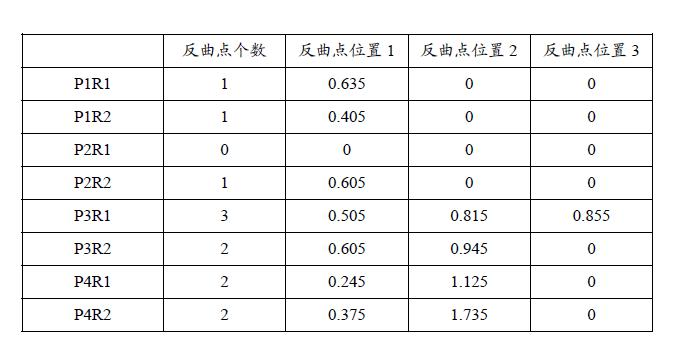
- Table 3 and Table 4 show the design data of the inflection point and stagnation point of each lens in the imaging optical lens 10 of the first embodiment of the present invention.
- P1R1, P1R2 represent the object side and image side of the first lens L1
- P2R1, P2R2 represent the object side and image side of the second lens L2
- P3R1, P3R2 represent the object side and image side of the third lens L3,
- P4R1 and P4R2 represent the object side and image side of the fourth lens L4, respectively.
- the corresponding data in the “reflection point position” column is the vertical distance from the reflex point set on the surface of each lens to the optical axis of the imaging optical lens 10.
- the data corresponding to the “stationary point position” column is the vertical distance from the stationary point set on the surface of each lens to the optical axis of the imaging optical lens 10.
- FIG. 4 shows a schematic diagram of field curvature and distortion of light with a wavelength of 588 nm after passing through the imaging optical lens 10 of the first embodiment.
- the field curvature S in FIG. 4 is the field curvature in the sagittal direction, and T is the field curvature in the meridian direction. .
- Table 13 shows the values corresponding to the various values in the first, second, and third embodiments and the parameters specified in the conditional expressions.
- the first embodiment satisfies various conditional expressions.
- the entrance pupil diameter of the imaging optical lens 10 is 1.243 mm
- the image height of the imaging optical lens 10 is 2.300 mm
- the diagonal field angle is 82.80°, so that the imaging optics
- the lens 10 has a wide-angle, ultra-thin, large aperture, and its on-axis and off-axis chromatic aberrations are fully corrected, and it has excellent optical characteristics.
- the second embodiment is basically the same as the first embodiment, and the meaning of the symbols is the same as that of the first embodiment. Please refer to FIG. 5 for the structure of the imaging optical lens 20 of the second embodiment. Only the differences are listed below.
- Table 5 and Table 6 show design data of the imaging optical lens 20 according to the second embodiment of the present invention.
- Table 6 shows aspheric surface data of each lens in the imaging optical lens 20 according to the second embodiment of the present invention.
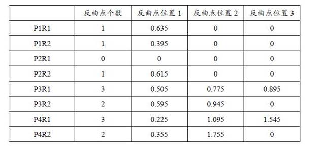
- Table 7 and Table 8 show the design data of the inflection point and stagnation point of each lens in the imaging optical lens 20 of the second embodiment of the present invention.
- FIG. 6 and 7 respectively show schematic diagrams of axial aberration and chromatic aberration of magnification after light having wavelengths of 486 nm, 588 nm, and 656 nm pass through the imaging optical lens 20 of the second embodiment.
- FIG. 8 shows a schematic diagram of field curvature and distortion of light with a wavelength of 588 nm after passing through the imaging optical lens 20 of the second embodiment.
- the field curvature S in FIG. 8 is the field curvature in the sagittal direction, and T is the field curvature in the meridian direction. .
- the entrance pupil diameter of the imaging optical lens 20 is 1.233 mm
- the image height of the imaging optical lens 10 is 2.300 mm
- the field angle of the diagonal direction is 80.00°, so that the imaging optical lens
- the lens 20 has a wide-angle, ultra-thin, large aperture, and its on-axis and off-axis chromatic aberrations are fully corrected, and it has excellent optical characteristics.
- the third embodiment is basically the same as the first embodiment, and the meaning of the symbols is the same as that of the first embodiment. Please refer to FIG. 9 for the structure of the imaging optical lens 30 of the third embodiment. Only the differences are listed below.
- Table 9 and Table 10 show design data of the imaging optical lens 30 of the third embodiment of the present invention.
- Table 10 shows the aspheric surface data of each lens in the imaging optical lens 30 of the third embodiment of the present invention.
- Table 11 and Table 12 show the design data of the inflection point and stagnation point of each lens in the imaging optical lens 30 of the third embodiment of the present invention.
- FIG. 10 and 11 respectively show schematic diagrams of axial aberration and chromatic aberration of magnification after light with wavelengths of 486 nm, 588 nm, and 656 nm pass through the imaging optical lens 30 of the third embodiment.
- FIG. 12 shows a schematic diagram of field curvature and distortion of light with a wavelength of 588 nm after passing through the imaging optical lens 30 of the third embodiment.
- the field curvature S in FIG. 12 is the field curvature in the sagittal direction, and T is the field curvature in the meridian direction. .
- the entrance pupil diameter of the imaging optical lens 30 is 1.041 mm
- the image height of the imaging optical lens 10 is 2.297 mm
- the field angle of the diagonal direction is 88.40°, so that the imaging optics
- the lens 30 has a wide-angle, ultra-thin, large aperture, and its on-axis and off-axis chromatic aberrations are fully corrected, and it has excellent optical characteristics.
- Fno is the aperture F number of the imaging optical lens.
Landscapes
- Physics & Mathematics (AREA)
- General Physics & Mathematics (AREA)
- Optics & Photonics (AREA)
- Lenses (AREA)
Abstract
一种摄像光学镜头(10,20,30),其自物侧至像侧依序包含:具有正屈折力的第一透镜(L1),具有负屈折力的第二透镜(L2),具有正屈折力的第三透镜(L3),以及具有负屈折力的第四透镜(L4);满足下列关系式:2.00≤(f1+f3)/f≤2.30;-8.60≤(f2+f4)/f≤-4.80;-2.10≤(R1+R2)/(R1-R2)≤-1.90;-4.00≤(R3+R4)/(R3-R4)≤-1.00;2.00≤(R7+R8)/(R7-R8)≤3.40。摄像光学镜头(10,20,30)具有良好光学性能的同时,满足大光圈、广角化、超薄化的设计要求。
Description
本发明涉及光学镜头领域,特别涉及一种适用于智能手机、数码相机等手提终端设备,以及监视器、PC镜头等摄像装置的摄像光学镜头。
近年来,随着智能手机的兴起,小型化摄影镜头的需求日渐提高,而一般摄影镜头的感光器件不外乎是感光耦合器件(Charge
Coupled Device,CCD)或互补性氧化金属半导体器件(Complementary
Metal-Oxide Semiconductor Sensor,CMOS
Sensor)两种,且由于半导体制造工艺技术的精进,使得感光器件的像素尺寸缩小,再加上现今电子产品以功能佳且轻薄短小的外型为发展趋势,因此,具备良好成像品质的小型化摄像镜头俨然成为目前市场上的主流。
为获得较佳的成像品质,传统搭载于手机相机的镜头多采用三片式透镜结构。然而,随着技术的发展以及用户多样化需求的增多,在感光器件的像素面积不断缩小,且系统对成像品质的要求不断提高的情况下,四片式透镜结构逐渐出现在镜头设计当中,常见的四片式透镜虽然已经具有较好的光学性能,但是其光焦度、透镜间距和透镜形状设置仍然具有一定的不合理性,导致透镜结构在具有良好光学性能的同时,无法满足大光圈、超薄化、广角化的设计要求。
针对上述问题,本发明的目的在于提供一种摄像光学镜头,其具有良好光学性能的同时,满足大光圈、超薄化、广角化的设计要求。
为解决上述技术问题,本发明的实施方式提供了一种所述摄像光学镜头,自物侧至像侧依序包含:具有正屈折力的第一透镜,具有负屈折力的第二透镜,具有正屈折力的第三透镜,以及具有负屈折力的第四透镜;
所述第一透镜的焦距为f1,所述第三透镜的焦距为f3,所述摄像光学镜头整体的焦距为f,所述第二透镜的焦距为f2,所述第四透镜的焦距为f4,所述第一透镜物侧面的曲率半径为R1,所述第一透镜像侧面的曲率半径为R2,所述第二透镜物侧面的曲率半径为R3,所述第二透镜像侧面的曲率半径为R4,所述第四透镜物侧面的曲率半径为R7,所述第四透镜像侧面的曲率半径为R8,满足下列关系式:
2.00
≤ (f1+ f3)
/f
≤2.30;
-8.60
≤ (f2+ f4)
/f
≤-4.80;
-2.10
≤ (R1+R2)
/(R1-R2)
≤-1.90;
-4.00
≤ (R3+R4)
/(R3-R4)
≤-1.00;
2.00
≤ (R7+R8)
/(R7-R8)
≤3.40。
优选的,所述第二透镜的轴上厚度为d3,所述第一透镜的像侧面到所述第二透镜的物侧面的轴上距离为d2,满足下列关系式:
0.70
≤d3/d2
≤0.85。
优选的,所述第一透镜的轴上厚度为d1,所述摄像光学镜头的光学长度为TTL,满足下列关系式:
0.54≤f1/f≤1.74;
0.06≤d1/TTL≤0.23。
优选的,所述第二透镜的轴上厚度为d3,所述摄像光学镜头的光学长度为TTL,满足下列关系式:
-14.72≤f2/f≤-2.47;
0.03≤d3/TTL≤0.11。
优选的,所述第三透镜的物侧面的曲率半径为R5,所述第三透镜的像侧面的曲率半径为R6,所述第三透镜的轴上厚度为d5,所述摄像光学镜头的光学长度为TTL,满足下列关系式:
0.45≤f3/f≤1.76;
1.36≤(R5+R6)/(R5-R6)≤4.51;
0.07≤d5/TTL≤0.23。
优选的,所述第四透镜的轴上厚度为d7,所述摄像光学镜头的光学长度为TTL,满足下列关系式:
-2.58≤f4/f≤-0.65;
0.04≤d7/TTL≤0.18。
优选的,所述摄像光学镜头的光学总长为TTL,所述摄像光学镜头的像高为IH,满足下列关系式:
TTL/IH≤1.37。
优选的,所述摄像光学镜头的视场角为FOV,满足下列关系式:
FOV≥80.00。
优选的,所述摄像光学镜头的光圈F数为Fno,满足下列关系式:
Fno≤2.27。
优选的,所述第一透镜与所述第二透镜的组合焦距为f12,满足下列关系式:
0.64≤f12/f≤2.08。
本发明的有益效果在于: 根据本发明的摄像光学镜头具有良好光学性能,且具有大光圈、广角化、超薄化的特性,尤其适用于由高像素用的CCD、CMOS等摄像元件构成的手机摄像镜头组件和WEB摄像镜头。
为了更清楚地说明本发明实施例中的技术方案,下面将对实施例描述中所需要使用的附图作简单地介绍,显而易见地,下面描述中的附图仅仅是本发明的一些实施例,对于本领域普通技术人员来讲,在不付出创造性劳动的前提下,还可以根据这些附图获得其它的附图,其中:
图1是实施方式一的摄像光学镜头的结构示意图;
图2是图1所示的摄像光学镜头的轴向像差示意图;
图3是图1所示的摄像光学镜头的倍率色差示意图;
图4是图1所示的摄像光学镜头的场曲及畸变示意图;
图5是实施方式二的摄像光学镜头的结构示意图;
图6是图5所示的摄像光学镜头的轴向像差示意图;
图7是图5所示的摄像光学镜头的倍率色差示意图;
图8是图5所示的摄像光学镜头的场曲及畸变示意图;
图9是实施方式三的摄像光学镜头的结构示意图;
图10是图9所示的摄像光学镜头的轴向像差示意图;
图11是图9所示的摄像光学镜头的倍率色差示意图;
图12是图9所示的摄像光学镜头的场曲及畸变示意图。
为使本发明的目的、技术方案和优点更加清楚,下面将结合附图对本发明的各实施方式进行详细的阐述。然而,本领域的普通技术人员可以理解,在本发明各实施方式中,为了使读者更好地理解本发明而提出了许多技术细节。但是,即使没有这些技术细节和基于以下各实施方式的种种变化和修改,也可以实现本发明所要求保护的技术方案。
(第一实施方式)
请参考附图,本发明提供了一种摄像光学镜头10。图1所示为本发明第一实施方式的摄像光学镜头10,该摄像光学镜头10包括四个透镜。具体的,所述摄像光学镜头10,由物侧至像侧依序包括:光圈S1、具有正屈折力的第一透镜L1、具有负屈折力的第二透镜L2、具有正屈折力的第三透镜L3以及具有负屈折力的第四透镜L4。所述第四透镜L4和像面Si之间可设置有光学过滤片(filter)GF等光学元件。
在本实施方式中,定义所述第一透镜L1的焦距为f1,所述第三透镜L3的焦距为f3,所述摄像光学镜头10整体的焦距为f,满足下列关系式:2.00
≤ (f1+f3)
/f
≤2.30,规定了所述第一透镜L1与所述第三透镜L3焦距的和与所述摄像光学镜头10整体的焦距的比值,可以有效地平衡由所述第一透镜L1产生的球差以及系统的场曲量。
定义所述第二透镜L2的焦距为f2,所述第四透镜L4的焦距为f4,所述摄像光学镜头10整体的焦距为f,满足下列关系式:-8.60
≤ (f2+f4)
/f
≤-4.80,规定了所述第二透镜L2与所述第四透镜L4焦距的和与所述摄像光学镜头10整体的焦距的比值,通过焦距的合理分配,使得系统具有较佳的成像品质和较低的敏感性。
定义所述第一透镜L1物侧面的曲率半径为R1,所述第一透镜L1像侧面的曲率半径为R2,满足下列关系式:-2.10
≤ (R1+R2)
/(R1-R2)
≤-1.90,规定了所述第一透镜L1的形状,在此条件范围内时,有利于补正轴上色像差。
定义所述第二透镜L2物侧面的曲率半径为R3,所述第二透镜L2像侧面的曲率半径为R4,满足下列关系式:-4.00
≤ (R3+R4)
/(R3-R4)
≤-1.00,规定了所述第二透镜L2的形状,在此条件范围内时,有利于所述第二透镜L2成型,并避免因表面曲率过大而导致成型不良与应力产生。
定义所述第四透镜L4物侧面的曲率半径为R7,所述第四透镜L4像侧面的曲率半径为R8,满足下列关系式:2.00
≤ (R7+R8)
/(R7-R8)
≤3.40,规定了所述第四透镜L4的形状,在此条件范围内时,有利于补正轴外画角的像差。
定义所述第二透镜L2的轴上厚度为d3,所述第一透镜L1的像侧面到所述第二透镜L2的物侧面的轴上距离为d2,满足下列关系式:0.70
≤d3/d2
≤0.85,规定了第二透镜厚度与所述第一透镜L1与所述第二透镜L2之间空气间隔的比值,在条件式范围内有助于压缩光学系统总长,实现超薄化效果。
定义所述第一透镜L1的焦距为f1,所述摄像光学镜头10整体的焦距为f,满足下列关系式:0.54≤f1/f≤1.74,规定了所述第一透镜L1的焦距与整体焦距的比值。在规定的范围内时,所述第一透镜L1具有适当的正屈折力,有利于减小系统像差,同时有利于镜头向超薄化、广角化发展。
所述第一透镜L1的轴上厚度为d1,所述摄像光学镜头10的光学总长为TTL,满足下列关系式:0.06≤d1/TTL≤0.23,在条件式范围内,有利于实现超薄化。
定义所述第二透镜L2的焦距为f2,所述摄像光学镜头10整体的焦距为f,满足下列关系式:-14.72≤f2/f≤-2.47,规定了第二透镜L2的焦距和所述摄像光学镜头10的焦距的比值,在条件式范围内,通过将第二透镜L2的负光焦度控制在合理范围,有利于矫正光学系统的像差。
所述第二透镜L2的轴上厚度为d3,所述摄像光学镜头10的光学总长为TTL,满足下列关系式:0.03≤d3/TTL≤0.11,在条件式范围内,有利于实现超薄化。
所述第三透镜L3的焦距为f3,满足下列关系式:0.45≤f3/f≤1.76,通过光焦度的合理分配,使得系统具有较佳的成像品质和较低的敏感性。
所述第三透镜L3的焦距为f3,所述第三透镜L3的物侧面的曲率半径为R5,所述第三透镜L3的像侧面的曲率半径为R6,满足下列关系式: 1.36≤(R5+R6)/(R5-R6)≤4.51,规定了第三透镜L3的形状,在条件式范围内,可以缓和光线经过镜片的偏折程度,有效减小像差。
所述第三透镜L3的轴上厚度为d5,所述摄像光学镜头10的光学总长为TTL,满足下列关系式:0.07≤d5/TTL≤0.23,在条件式范围内,有利于实现超薄化。
定义所述第四透镜L4的焦距为f4,所述摄像光学镜头10整体的焦距为f,且满足下列关系式:-2.58≤f4/f≤-0.65,在条件式范围内,通过光焦度的合理分配,使得系统具有较佳的成像品质,有助于提高光学系统性能。
所述第四透镜L4的轴上厚度为d7,所述摄像光学镜头10的光学总长为TTL,满足下列关系式:0.04≤d7/TTL≤0.18,在条件式范围内,有利于实现超薄化。
进一步的,定义所述摄像光学镜头10的光学总长为TTL,所述摄像光学镜头10的像高为IH,满足下列关系式:TTL/IH≤1.37,有利于实现超薄化。
本实施方式中,所述摄像光学镜头10对角线方向的视场角为FOV,且满足下列关系式:FOV≥80.00,有利于实现广角化。
定义所述摄像光学镜头10的光圈F数为Fno,满足下列关系式:Fno≤2.27,有利于实现大光圈,使得成像性能好。
定义所述第一透镜L1与所述第二透镜L2的组合焦距为f12,满足下列关系式:0.64≤f12/f≤2.08,在条件式范围内,可消除所述摄像光学镜头10的像差与歪曲,且可压制摄像光学镜头10后焦距,维持影像镜片系统组小型化。
即当满足上述关系时,使得摄像光学镜头10实现了在具有良好光学成像性能的同时,还能满足大光圈、广角化、超薄化的设计要求;根据该摄像光学镜头10的特性,该摄像光学镜头10尤其适用于由高像素用的CCD、CMOS等摄像元件构成的手机摄像镜头组件和WEB摄像镜头。
下面将用实例进行说明本发明的摄像光学镜头10。各实例中所记载的符号如下所示。焦距、轴上距离、曲率半径、轴上厚度、反曲点位置、驻点位置的单位为mm。
TTL:光学总长(第一透镜L1的物侧面到像面Si的轴上距离),单位为mm;
优选的,所述透镜的物侧面和/或像侧面上还可以设置有反曲点和/或驻点,以满足高品质的成像需求,具体的可实施方案,参下所述。
表1、表2示出本发明第一实施方式的摄像光学镜头10的设计数据。
【表1】

其中,各符号的含义如下。
S1: 光圈;
R: 光学面的曲率半径、透镜时为中心曲率半径;
R1: 第一透镜L1的物侧面的曲率半径;
R2: 第一透镜L1的像侧面的曲率半径;
R3: 第二透镜L2的物侧面的曲率半径;
R4: 第二透镜L2的像侧面的曲率半径;
R5: 第三透镜L3的物侧面的曲率半径;
R6: 第三透镜L3的像侧面的曲率半径;
R7: 第四透镜L4的物侧面的曲率半径;
R8: 第四透镜L4的像侧面的曲率半径;
R9:光学过滤片GF的物侧面的曲率半径;
R10:光学过滤片GF的像侧面的曲率半径;
d: 透镜的轴上厚度与透镜之间的轴上距离;
d0: 光圈S1到第一透镜L1的物侧面的轴上距离;
d1: 第一透镜L1的轴上厚度;
d2: 第一透镜L1的像侧面到第二透镜L2的物侧面的轴上距离;
d3: 第二透镜L2的轴上厚度;
d4: 第二透镜L2的像侧面到第三透镜L3的物侧面的轴上距离;
d5: 第三透镜L3的轴上厚度;
d6: 第三透镜L3的像侧面到第四透镜L4的物侧面的轴上距离;
d7: 第四透镜L4的轴上厚度;
d8: 第四透镜L4的像侧面到光学过滤片GF的物侧面的轴上距离;
d9:光学过滤片GF的轴上厚度;
d10:光学过滤片GF的像侧面到像面的轴上距离;
nd: d线的折射率;
nd1:第一透镜L1的d线的折射率;
nd2:第二透镜L2的d线的折射率;
nd3:第三透镜L3的d线的折射率;
nd4:第四透镜L4的d线的折射率;
ndg:光学过滤片GF的d线的折射率;
νd:阿贝数;
ν1:第一透镜L1的阿贝数;
ν2:第二透镜L2的阿贝数;
ν3:第三透镜L3的阿贝数;
ν4:第四透镜L4的阿贝数;
νg:光学过滤片GF的阿贝数。
表2示出本发明第一实施方式的摄像光学镜头10中各透镜的非球面数据。
【表2】

其中,k是圆锥系数,A4、A6、A8、A10、A12、A14、A16是非球面系数。
y=(x
2/R)/[1+{1-(k+1)(x
2/R
2)}
1/2]+A4x
4+A6x
6+A8x
8+A10x
10+A12x
12+A14x
14+A16x
16
(1)
为方便起见,各个透镜面的非球面使用上述公式(1)中所示的非球面。但是,本发明不限于该公式(1)表示的非球面多项式形式。
表3、表4示出本发明第一实施方式的摄像光学镜头10中各透镜的反曲点以及驻点设计数据。其中,P1R1、P1R2分别代表第一透镜L1的物侧面和像侧面, P2R1、P2R2分别代表第二透镜L2的物侧面和像侧面,P3R1、P3R2分别代表第三透镜L3的物侧面和像侧面,P4R1、P4R2分别代表第四透镜L4的物侧面和像侧面。“反曲点位置”栏位对应数据为各透镜表面所设置的反曲点到摄像光学镜头10光轴的垂直距离。“驻点位置”栏位对应数据为各透镜表面所设置的驻点到摄像光学镜头10光轴的垂直距离。
【表3】
【表4】
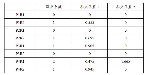
图2、图3分别示出了波长为486nm、588nm和656nm的光经过第一实施方式的摄像光学镜头10后的轴向像差和倍率色差示意图。图4则示出了波长为588nm的光经过第一实施方式的摄像光学镜头10后的场曲及畸变示意图,图4的场曲S是弧矢方向的场曲,T是子午方向的场曲。
后出现的表13示出各实施方式一、二、三中各种数值与条件式中已规定的参数所对应的值。
如表13所示,第一实施方式满足各条件式。
在本实施方式中,所述摄像光学镜头10的入瞳直径为1.243mm,所述摄像光学镜头10的像高为2.300mm,对角线方向的视场角为82.80°,使得所述摄像光学镜头10广角化、超薄化、大光圈,其轴上、轴外色像差充分补正,且具有优秀的光学特征。
(第二实施方式)
第二实施方式与第一实施方式基本相同,符号含义与第一实施方式相同,该第二实施方式的摄像光学镜头20的结构形式请参图5所示,以下只列出不同点。
表5、表6示出本发明第二实施方式的摄像光学镜头20的设计数据。
【表5】

表6示出本发明第二实施方式的摄像光学镜头20中各透镜的非球面数据。
【表6】
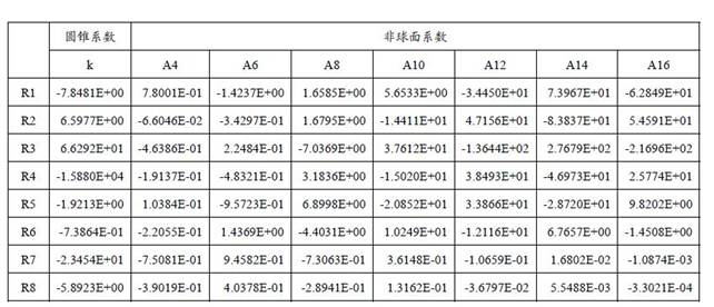
表7、表8示出本发明第二实施方式的摄像光学镜头20中各透镜的反曲点以及驻点设计数据。
【表7】
【表8】

图6和图7分别示出了波长为486nm、588nm和656nm的光经过第二实施方式的摄像光学镜头20后的轴向像差和倍率色差示意图。图8则示出了波长为588nm的光经过第二实施方式的摄像光学镜头20后的场曲及畸变示意图,图8的场曲S是弧矢方向的场曲,T是子午方向的场曲。
以下表13按照上述条件式列出了本实施方式中对应各条件式的数值。显然,本实施方式的摄像光学镜头20满足上述的条件式。
在本实施方式中,所述摄像光学镜头20的入瞳直径为1.233mm,所述摄像光学镜头10的像高为2.300mm,对角线方向的视场角为80.00°,使得所述摄像光学镜头20广角化、超薄化、大光圈,其轴上、轴外色像差充分补正,且具有优秀的光学特征。
(第三实施方式)
第三实施方式与第一实施方式基本相同,符号含义与第一实施方式相同,该第三实施方式的摄像光学镜头30的结构形式请参图9所示,以下只列出不同点。
表9、表10示出本发明第三实施方式的摄像光学镜头30的设计数据。
【表9】

表10示出本发明第三实施方式的摄像光学镜头30中各透镜的非球面数据。
【表10】

表11、表12示出本发明第三实施方式的摄像光学镜头30中各透镜的反曲点以及驻点设计数据。
【表11】

【表12】

图10和图11分别示出了波长为486nm、588nm和656nm的光经过第三实施方式的摄像光学镜头30后的轴向像差和倍率色差示意图。图12则示出了波长为588nm的光经过第三实施方式的摄像光学镜头30后的场曲及畸变示意图,图12的场曲S是弧矢方向的场曲,T是子午方向的场曲。
以下表13按照上述条件式列出了本实施方式中对应各条件式的数值。显然,本实施方式的摄像光学镜头30满足上述的条件式。
在本实施方式中,所述摄像光学镜头30的入瞳直径为1.041mm,所述摄像光学镜头10的像高为2.297mm,对角线方向的视场角为88.40°,使得所述摄像光学镜头30广角化、超薄化、大光圈,其轴上、轴外色像差充分补正,且具有优秀的光学特征。
【表13】

其中,Fno为摄像光学镜头的光圈F数。
本领域的普通技术人员可以理解,上述各实施方式是实现本发明的具体实施方式,而在实际应用中,可以在形式上和细节上对其作各种改变,而不偏离本发明的精神和范围。
Claims (10)
- 一种摄像光学镜头,其特征在于,所述摄像光学镜头,自物侧至像侧依序包含:具有正屈折力的第一透镜,具有负屈折力的第二透镜,具有正屈折力的第三透镜,以及具有负屈折力的第四透镜;所述第一透镜的焦距为f1,所述第三透镜的焦距为f3,所述摄像光学镜头整体的焦距为f,所述第二透镜的焦距为f2,所述第四透镜的焦距为f4,所述第一透镜物侧面的曲率半径为R1,所述第一透镜像侧面的曲率半径为R2,所述第二透镜物侧面的曲率半径为R3,所述第二透镜像侧面的曲率半径为R4,所述第四透镜物侧面的曲率半径为R7,所述第四透镜像侧面的曲率半径为R8,满足下列关系式:2.00 ≤ (f1+ f3) /f ≤2.30;-8.60 ≤ (f2+ f4) /f ≤-4.80;-2.10 ≤ (R1+R2) /(R1-R2) ≤-1.90;-4.00 ≤ (R3+R4) /(R3-R4) ≤-1.00;2.00 ≤ (R7+R8) /(R7-R8) ≤3.40。
- 根据权利要求1所述的摄像光学镜头,其特征在于,所述第二透镜的轴上厚度为d3,所述第一透镜的像侧面到所述第二透镜的物侧面的轴上距离为d2,满足下列关系式:0.70 ≤d3/d2 ≤0.85。
- 根据权利要求1所述的摄像光学镜头,其特征在于,所述第一透镜的轴上厚度为d1,所述摄像光学镜头的光学长度为TTL,满足下列关系式:0.54≤f1/f≤1.74;0.06≤d1/TTL≤0.23。
- 根据权利要求1所述的摄像光学镜头,其特征在于,所述第二透镜的轴上厚度为d3,所述摄像光学镜头的光学长度为TTL,满足下列关系式:-14.72≤f2/f≤-2.47;0.03≤d3/TTL≤0.11。
- 根据权利要求1所述的摄像光学镜头,其特征在于,所述第三透镜的物侧面的曲率半径为R5,所述第三透镜的像侧面的曲率半径为R6,所述第三透镜的轴上厚度为d5,所述摄像光学镜头的光学长度为TTL,满足下列关系式:0.45≤f3/f≤1.76;1.36≤(R5+R6)/(R5-R6)≤4.51;0.07≤d5/TTL≤0.23。
- 根据权利要求1所述的摄像光学镜头,其特征在于,所述第四透镜的轴上厚度为d7,所述摄像光学镜头的光学长度为TTL,满足下列关系式:-2.58≤f4/f≤-0.65;0.04≤d7/TTL≤0.18。
- 根据权利要求1所述的摄像光学镜头,其特征在于,所述摄像光学镜头的光学总长为TTL,所述摄像光学镜头的像高为IH,满足下列关系式:TTL/IH≤1.37。
- 根据权利要求1所述的摄像光学镜头,其特征在于,所述摄像光学镜头的视场角为FOV,满足下列关系式:FOV≥80.00。
- 根据权利要求1所述的摄像光学镜头,其特征在于,所述摄像光学镜头的光圈F数为Fno,满足下列关系式:
- 根据权利要求1所述的摄像光学镜头,其特征在于,所述第一透镜与所述第二透镜的组合焦距为f12,满足下列关系式:0.64≤f12/f≤2.08。
Applications Claiming Priority (2)
| Application Number | Priority Date | Filing Date | Title |
|---|---|---|---|
| CN201910760920.6 | 2019-08-16 | ||
| CN201910760920.6A CN110488462B (zh) | 2019-08-16 | 2019-08-16 | 摄像光学镜头 |
Publications (1)
| Publication Number | Publication Date |
|---|---|
| WO2021031277A1 true WO2021031277A1 (zh) | 2021-02-25 |
Family
ID=68551895
Family Applications (1)
| Application Number | Title | Priority Date | Filing Date |
|---|---|---|---|
| PCT/CN2019/107153 Ceased WO2021031277A1 (zh) | 2019-08-16 | 2019-09-21 | 摄像光学镜头 |
Country Status (4)
| Country | Link |
|---|---|
| US (1) | US11454784B2 (zh) |
| JP (1) | JP6919038B2 (zh) |
| CN (1) | CN110488462B (zh) |
| WO (1) | WO2021031277A1 (zh) |
Families Citing this family (5)
| Publication number | Priority date | Publication date | Assignee | Title |
|---|---|---|---|---|
| WO2021195891A1 (zh) * | 2020-03-30 | 2021-10-07 | 江西晶超光学有限公司 | 光学成像系统、取像装置及电子设备 |
| KR20230021283A (ko) | 2021-08-05 | 2023-02-14 | 삼성전자주식회사 | 렌즈 어셈블리 및 그를 포함하는 전자 장치 |
| CN113721351B (zh) * | 2021-11-04 | 2022-04-19 | 江西联益光学有限公司 | 光学镜头及成像设备 |
| CN114236864B (zh) * | 2021-11-23 | 2024-07-16 | 青岛歌尔声学科技有限公司 | 光学模组及头戴显示设备 |
| CN114815183B (zh) * | 2022-04-28 | 2023-11-24 | 广东旭业光电科技股份有限公司 | 一种高像质光学成像系统及拍摄装置 |
Citations (6)
| Publication number | Priority date | Publication date | Assignee | Title |
|---|---|---|---|---|
| CN101561548A (zh) * | 2008-04-15 | 2009-10-21 | 柯尼卡美能达精密光学株式会社 | 摄像镜头、摄像单元及便携终端 |
| US20090290234A1 (en) * | 2008-05-21 | 2009-11-26 | Konica Minolta Opto, Inc. | Image Pickup Lens, Image Pickup Unit, and Mobile Terminal |
| CN102540424A (zh) * | 2010-12-14 | 2012-07-04 | 索尼公司 | 成像透镜和成像设备 |
| CN104614838A (zh) * | 2013-11-01 | 2015-05-13 | 大立光电股份有限公司 | 成像透镜组、取像装置以及可携式装置 |
| JP2015138174A (ja) * | 2014-01-23 | 2015-07-30 | アウラディアス合同会社 | 撮像レンズ |
| CN105892015A (zh) * | 2016-02-24 | 2016-08-24 | 瑞声科技(新加坡)有限公司 | 摄像镜头 |
Family Cites Families (15)
| Publication number | Priority date | Publication date | Assignee | Title |
|---|---|---|---|---|
| JP5069554B2 (ja) * | 2007-12-28 | 2012-11-07 | カンタツ株式会社 | 撮像レンズ |
| JP4556148B2 (ja) * | 2008-07-23 | 2010-10-06 | ソニー株式会社 | 撮像レンズ及び撮像装置 |
| TWI422898B (zh) * | 2011-05-03 | 2014-01-11 | Largan Precision Co Ltd | 影像拾取系統 |
| JP5644681B2 (ja) * | 2011-06-03 | 2014-12-24 | コニカミノルタ株式会社 | 撮像装置及び携帯端末 |
| JP2013092584A (ja) * | 2011-10-24 | 2013-05-16 | Konica Minolta Advanced Layers Inc | 撮像レンズ、撮像装置及び携帯端末 |
| TWI439751B (zh) * | 2011-12-02 | 2014-06-01 | Largan Precision Co Ltd | 成像鏡片系統 |
| TWI516790B (zh) * | 2012-08-27 | 2016-01-11 | 玉晶光電股份有限公司 | Optical imaging lens and the application of the lens of the electronic device |
| TW201520634A (zh) * | 2013-11-29 | 2015-06-01 | Showin Technology Co Ltd | 小型化定焦鏡頭 |
| CN103969791B (zh) * | 2013-12-09 | 2016-05-25 | 玉晶光电(厦门)有限公司 | 光学成像镜头及应用此镜头的电子装置 |
| CN105629434B (zh) * | 2014-11-06 | 2018-04-03 | 玉晶光电(厦门)有限公司 | 光学成像镜头及应用该光学成像镜头的电子装置 |
| JP6358752B2 (ja) * | 2015-12-25 | 2018-07-18 | カンタツ株式会社 | 撮像レンズ |
| TWI587000B (zh) * | 2016-02-02 | 2017-06-11 | 大立光電股份有限公司 | 取像系統鏡組、取像裝置及電子裝置 |
| JP5953450B1 (ja) * | 2016-04-08 | 2016-07-20 | エーエーシー テクノロジーズ ピーティーイー リミテッドAac Technologies Pte.Ltd. | 撮像レンズ |
| CN208092314U (zh) * | 2018-04-20 | 2018-11-13 | 南昌欧菲精密光学制品有限公司 | 光学镜头 |
| CN208654422U (zh) * | 2018-08-23 | 2019-03-26 | 南昌欧菲精密光学制品有限公司 | 摄影镜头、取像装置及电子装置 |
-
2019
- 2019-08-16 CN CN201910760920.6A patent/CN110488462B/zh active Active
- 2019-09-21 WO PCT/CN2019/107153 patent/WO2021031277A1/zh not_active Ceased
-
2020
- 2020-08-03 JP JP2020131961A patent/JP6919038B2/ja active Active
- 2020-08-12 US US16/992,018 patent/US11454784B2/en active Active
Patent Citations (6)
| Publication number | Priority date | Publication date | Assignee | Title |
|---|---|---|---|---|
| CN101561548A (zh) * | 2008-04-15 | 2009-10-21 | 柯尼卡美能达精密光学株式会社 | 摄像镜头、摄像单元及便携终端 |
| US20090290234A1 (en) * | 2008-05-21 | 2009-11-26 | Konica Minolta Opto, Inc. | Image Pickup Lens, Image Pickup Unit, and Mobile Terminal |
| CN102540424A (zh) * | 2010-12-14 | 2012-07-04 | 索尼公司 | 成像透镜和成像设备 |
| CN104614838A (zh) * | 2013-11-01 | 2015-05-13 | 大立光电股份有限公司 | 成像透镜组、取像装置以及可携式装置 |
| JP2015138174A (ja) * | 2014-01-23 | 2015-07-30 | アウラディアス合同会社 | 撮像レンズ |
| CN105892015A (zh) * | 2016-02-24 | 2016-08-24 | 瑞声科技(新加坡)有限公司 | 摄像镜头 |
Also Published As
| Publication number | Publication date |
|---|---|
| JP2021033286A (ja) | 2021-03-01 |
| US20210048616A1 (en) | 2021-02-18 |
| CN110488462B (zh) | 2021-08-20 |
| JP6919038B2 (ja) | 2021-08-11 |
| CN110488462A (zh) | 2019-11-22 |
| US11454784B2 (en) | 2022-09-27 |
Similar Documents
| Publication | Publication Date | Title |
|---|---|---|
| CN110231705B (zh) | 摄像光学镜头 | |
| WO2021031276A1 (zh) | 摄像光学镜头 | |
| WO2021237781A1 (zh) | 摄像光学镜头 | |
| WO2021031282A1 (zh) | 摄像光学镜头 | |
| WO2021031284A1 (zh) | 摄像光学镜头 | |
| WO2021031275A1 (zh) | 摄像光学镜头 | |
| WO2021031285A1 (zh) | 摄像光学镜头 | |
| WO2022021513A1 (zh) | 摄像光学镜头 | |
| WO2021031278A1 (zh) | 摄像光学镜头 | |
| WO2021031274A1 (zh) | 摄像光学镜头 | |
| WO2021027022A1 (zh) | 摄像光学镜头 | |
| WO2021031283A1 (zh) | 摄像光学镜头 | |
| WO2021097953A1 (zh) | 摄像光学镜头 | |
| WO2022047985A1 (zh) | 摄像光学镜头 | |
| WO2021109198A1 (zh) | 摄像光学镜头 | |
| WO2021097929A1 (zh) | 摄像光学镜头 | |
| CN110488462A (zh) | 摄像光学镜头 | |
| WO2021168884A1 (zh) | 摄像光学镜头 | |
| WO2021168879A1 (zh) | 摄像光学镜头 | |
| WO2021031281A1 (zh) | 摄像光学镜头 | |
| WO2021114235A1 (zh) | 摄像光学镜头 | |
| CN107918195A (zh) | 摄像光学镜头 | |
| WO2021168886A1 (zh) | 摄像光学镜头 | |
| CN110398817A (zh) | 摄像光学镜头 | |
| WO2021114242A1 (zh) | 摄像光学镜头 |
Legal Events
| Date | Code | Title | Description |
|---|---|---|---|
| 121 | Ep: the epo has been informed by wipo that ep was designated in this application |
Ref document number: 19942539 Country of ref document: EP Kind code of ref document: A1 |
|
| NENP | Non-entry into the national phase |
Ref country code: DE |
|
| 122 | Ep: pct application non-entry in european phase |
Ref document number: 19942539 Country of ref document: EP Kind code of ref document: A1 |