WO2021029286A1 - 表示装置 - Google Patents
表示装置 Download PDFInfo
- Publication number
- WO2021029286A1 WO2021029286A1 PCT/JP2020/029883 JP2020029883W WO2021029286A1 WO 2021029286 A1 WO2021029286 A1 WO 2021029286A1 JP 2020029883 W JP2020029883 W JP 2020029883W WO 2021029286 A1 WO2021029286 A1 WO 2021029286A1
- Authority
- WO
- WIPO (PCT)
- Prior art keywords
- electrode
- substrate
- light emitting
- display device
- layer
- Prior art date
- Legal status (The legal status is an assumption and is not a legal conclusion. Google has not performed a legal analysis and makes no representation as to the accuracy of the status listed.)
- Ceased
Links
Images











Classifications
-
- F—MECHANICAL ENGINEERING; LIGHTING; HEATING; WEAPONS; BLASTING
- F21—LIGHTING
- F21K—NON-ELECTRIC LIGHT SOURCES USING LUMINESCENCE; LIGHT SOURCES USING ELECTROCHEMILUMINESCENCE; LIGHT SOURCES USING CHARGES OF COMBUSTIBLE MATERIAL; LIGHT SOURCES USING SEMICONDUCTOR DEVICES AS LIGHT-GENERATING ELEMENTS; LIGHT SOURCES NOT OTHERWISE PROVIDED FOR
- F21K2/00—Non-electric light sources using luminescence; Light sources using electrochemiluminescence
- F21K2/06—Non-electric light sources using luminescence; Light sources using electrochemiluminescence using chemiluminescence
- F21K2/08—Non-electric light sources using luminescence; Light sources using electrochemiluminescence using chemiluminescence activated by an electric field, i.e. electrochemiluminescence
-
- F—MECHANICAL ENGINEERING; LIGHTING; HEATING; WEAPONS; BLASTING
- F21—LIGHTING
- F21S—NON-PORTABLE LIGHTING DEVICES; SYSTEMS THEREOF; VEHICLE LIGHTING DEVICES SPECIALLY ADAPTED FOR VEHICLE EXTERIORS
- F21S2/00—Systems of lighting devices, not provided for in main groups F21S4/00 - F21S10/00 or F21S19/00, e.g. of modular construction
-
- G—PHYSICS
- G02—OPTICS
- G02F—OPTICAL DEVICES OR ARRANGEMENTS FOR THE CONTROL OF LIGHT BY MODIFICATION OF THE OPTICAL PROPERTIES OF THE MEDIA OF THE ELEMENTS INVOLVED THEREIN; NON-LINEAR OPTICS; FREQUENCY-CHANGING OF LIGHT; OPTICAL LOGIC ELEMENTS; OPTICAL ANALOGUE/DIGITAL CONVERTERS
- G02F1/00—Devices or arrangements for the control of the intensity, colour, phase, polarisation or direction of light arriving from an independent light source, e.g. switching, gating or modulating; Non-linear optics
- G02F1/01—Devices or arrangements for the control of the intensity, colour, phase, polarisation or direction of light arriving from an independent light source, e.g. switching, gating or modulating; Non-linear optics for the control of the intensity, phase, polarisation or colour
- G02F1/13—Devices or arrangements for the control of the intensity, colour, phase, polarisation or direction of light arriving from an independent light source, e.g. switching, gating or modulating; Non-linear optics for the control of the intensity, phase, polarisation or colour based on liquid crystals, e.g. single liquid crystal display cells
- G02F1/133—Constructional arrangements; Operation of liquid crystal cells; Circuit arrangements
- G02F1/1333—Constructional arrangements; Manufacturing methods
- G02F1/1335—Structural association of cells with optical devices, e.g. polarisers or reflectors
-
- G—PHYSICS
- G02—OPTICS
- G02F—OPTICAL DEVICES OR ARRANGEMENTS FOR THE CONTROL OF LIGHT BY MODIFICATION OF THE OPTICAL PROPERTIES OF THE MEDIA OF THE ELEMENTS INVOLVED THEREIN; NON-LINEAR OPTICS; FREQUENCY-CHANGING OF LIGHT; OPTICAL LOGIC ELEMENTS; OPTICAL ANALOGUE/DIGITAL CONVERTERS
- G02F1/00—Devices or arrangements for the control of the intensity, colour, phase, polarisation or direction of light arriving from an independent light source, e.g. switching, gating or modulating; Non-linear optics
- G02F1/01—Devices or arrangements for the control of the intensity, colour, phase, polarisation or direction of light arriving from an independent light source, e.g. switching, gating or modulating; Non-linear optics for the control of the intensity, phase, polarisation or colour
- G02F1/13—Devices or arrangements for the control of the intensity, colour, phase, polarisation or direction of light arriving from an independent light source, e.g. switching, gating or modulating; Non-linear optics for the control of the intensity, phase, polarisation or colour based on liquid crystals, e.g. single liquid crystal display cells
- G02F1/137—Devices or arrangements for the control of the intensity, colour, phase, polarisation or direction of light arriving from an independent light source, e.g. switching, gating or modulating; Non-linear optics for the control of the intensity, phase, polarisation or colour based on liquid crystals, e.g. single liquid crystal display cells characterised by the electro-optical or magneto-optical effect, e.g. field-induced phase transition, orientation effect, guest-host interaction or dynamic scattering
-
- G—PHYSICS
- G09—EDUCATION; CRYPTOGRAPHY; DISPLAY; ADVERTISING; SEALS
- G09F—DISPLAYING; ADVERTISING; SIGNS; LABELS OR NAME-PLATES; SEALS
- G09F9/00—Indicating arrangements for variable information in which the information is built-up on a support by selection or combination of individual elements
Definitions
- One embodiment of the present invention relates to a display device having an electrochemical light emitting cell (LEC: Light-emmitting Electrochemical Cell) and a method for manufacturing the display device.
- LEC Light-emmitting Electrochemical Cell
- Examples of display devices include liquid crystal display devices, organic EL (Electroluminescence: EL) display devices, and the like.
- the liquid crystal display device has a liquid crystal element in each of a plurality of pixels formed on the substrate.
- the liquid crystal element has a liquid crystal layer between a pair of electrodes, and is driven by applying a voltage between the pair of electrodes.
- the organic EL display device has a light emitting element in each of a plurality of pixels formed on the substrate.
- the light emitting element has an organic layer containing an organic compound exhibiting electroluminescence between the pair of electrodes, and is driven by passing an electric current between the pair of electrodes.
- the mainstream backlight for liquid crystal display devices is the edge light method, which has a plurality of LED mounts at positions overlapping one end of the liquid crystal display device.
- the point-shaped light from the plurality of LEDs is emitted to the liquid crystal display device in place of the planar light by the light guide plate, the diffusion film, and the reflective film.
- each is configured by laminating optical films of about several tens of ⁇ m to several hundreds of ⁇ m.
- the liquid crystal panel is provided with polarizing plates on the display surface side and the surface opposite to the display surface, respectively.
- the liquid crystal display device is configured by laminating a liquid crystal panel on a backlight. Therefore, there is a problem that the total thickness of these is larger than the total thickness of the organic EL display device due to the thickness of the backlight and the thickness of the liquid crystal panel.
- one of the objects of the embodiment of the present invention is to reduce the total thickness of the display device.
- the display device has a first substrate having a first surface and a second surface opposite to the first surface, and a third surface having a third surface and a fourth surface opposite to the third surface.
- the two substrates the guest host liquid crystal layer provided between the first surface of the first substrate and the fourth surface of the second substrate, the first electrode provided on the second surface of the first substrate, and the luminescent polymer.
- an ionic liquid a light emitting layer provided on the surface of the first electrode opposite to the first substrate, and a second electrode provided so as to face the first electrode with the light emitting layer sandwiched between them. It has a polarizing plate provided on the third surface of the second substrate.
- the display device has a first substrate having a first surface and a second surface opposite to the first surface, and a third surface having a third surface and a fourth surface opposite to the third surface.
- a light emitting layer containing two substrates, a second electrode provided on the first surface of the first substrate, a light emitting polymer and an ionic liquid, and provided on the second electrode, and a first light emitting layer provided on the light emitting layer. It has an electrode, a guest host liquid crystal layer provided between the first electrode and the fourth surface of the second substrate, and a polarizing plate provided on the third surface of the second substrate.
- the display device has a first substrate having a first surface and a second surface opposite to the first surface, and a third surface having a third surface and a fourth surface opposite to the third surface.
- Two substrates a guest host liquid crystal provided on the first surface of the first substrate, a black matrix and a color filter provided on the fourth surface of the second substrate, and a second electrode provided on the black matrix. It contains a light emitting polymer and an ionic liquid, and has a light emitting layer provided on the second electrode, a first electrode provided on the light emitting layer, and a polarizing plate provided on the third surface of the second substrate. ..
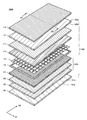
- FIG. 1 is a developed view of a display device according to an embodiment of the present invention
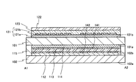
- FIG. 2 is a cross-sectional view when the display device 100 shown in FIG. 1 is cut along lines A1-A2.
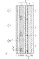
- FIG. 3 is an enlarged cross-sectional view of a part of the display device 100 shown in FIG.
- the display device 100 shown in FIGS. 1 to 3 includes a liquid crystal panel 110, an electrochemical light emitting cell 120, and a polarizing plate 114.
- the electrochemical light emitting cell 120 functions as a backlight of the liquid crystal panel 110.
- the surface on which the polarizing plate 114 is provided on the second substrate 102 will be described as being the display surface side of the display device 100.
- the surface of the second substrate 102 on which the polarizing plate 114 is provided will be referred to as the first surface 102a, and the surface on the opposite side will be referred to as the second surface 102b.
- the display surface side will be referred to as the first surface 101a, and the opposite surface will be referred to as the second surface 101b.
- the electrochemical light emitting cell 120 is provided on the second surface 101b side of the first substrate 101.
- the electrochemical light-emitting cell 120 has a structure in which a light-emitting layer 123 containing a light-emitting polymer and an ionic liquid is sandwiched between a first electrode 121 and a second electrode 122.
- the light emitting layer 123 contains both electrons and ions, and by applying a voltage between the first electrode 121 and the second electrode 122, a p-in bond is spontaneously formed.
- the light emitting layer 123 emits light.
- the ionic liquid means an organic salt that is liquid at room temperature.
- the first electrode 121 has an oxide conductive layer 121a and a metal conductive layer 121b.
- the oxide conductive layer 121a is a light-transmitting conductive layer, and is formed on substantially the entire surface of the first substrate 101 on the second surface 101b side.
- the oxide conductive layer 121a has a higher resistance than the metal conductive layer 121b. Therefore, when the oxide conductive layer 121a is provided on substantially the entire surface of the second surface 101b of the first substrate 101, when a potential is supplied to one end of the first electrode 121, the potential is attenuated at the other end to emit light. The brightness becomes uneven.
- the overall resistance of the first electrode 121 is lowered by providing the metal conductive layer 121b having a plurality of openings so as to be superimposed on the oxide conductive layer 121a.
- the potential supplied to one end of the first electrode 121 can suppress the attenuation of the potential even at the other end, and the unevenness of the emission brightness can be suppressed.
- the film thickness of the oxide conductive layer 121a is, for example, about 75 nm (50 nm to 100 nm), and the film thickness of the metal conductive layer 121b is about 600 nm (550 nm to 650 nm). Further, the total thickness of the first electrode 121 is preferably less than 1 ⁇ m.
- the pattern having a plurality of openings provided in the metal conductive layer 121b is, for example, a grid shape or a mesh shape in which the wiring is thinned to the extent that it cannot be visually recognized.
- the grid pattern is a structure having a pattern in which a plurality of wirings extending in the first direction D1 and a plurality of wirings extending in the second direction D2 intersect at right angles.
- the mesh shape is specifically a structure having a pattern in which a plurality of wirings intersect at an angle other than the above-mentioned direct intersection.
- the opening formed by these plurality of wirings has a rhombus shape or a parallel quadrilateral shape.
- the wiring width forming the pattern having a plurality of openings is preferably 1 ⁇ m or more and 10 ⁇ m or less, for example.
- the oxide conductive layer 121a of the first electrode 121 may be in contact with the second surface 101b of the first substrate 101, the metal conductive layer 121b may be in contact with the light emitting layer 123, and the metal conductive layer 121b may be in contact with the first substrate 101.
- the oxide conductive layer 121a may be in contact with the two surfaces 101b and the light emitting layer 123.
- the oxide conductive layer 121a for example, indium tin oxide (Indium Tin Oxide; ITO) and indium zinc oxide (Indium Zinc Oxide; IZO) are used.
- an MgAg thin film may be used instead of the oxide conductive layer 121a.
- the metal conductive layer 121b for example, titanium, aluminum, and titanium are laminated and used.
- the light emitting layer 123 is formed on almost the entire surface of the first electrode 121 and contains a light emitting polymer and an ionic liquid.
- the light emitting color of the light emitting layer 123 is preferably white.
- the film thickness of the light emitting layer 123 is about 100 nm (90 nm to 200 nm).
- the second electrode 122 is formed on almost the entire surface of the light emitting layer 123 by using the metal conductive layer.
- the second electrode 122 has a metal conductive layer having high reflectance.
- the metal layer having high reflectance reflects the light emitted from the light emitting layer 123, passes through the first electrode 121, and emits light from the second substrate 102.
- aluminum is used as the second electrode 122.
- the film thickness of the second electrode 122 is 50 nm to 100 nm.
- the thickness of the electrochemical light emitting cell 120 is the total thickness of the first electrode 121, the light emitting layer 123, and the second electrode 122, and is 740 nm to 1050 nm.
- the thickness of the polarizing plate 114 is 50 ⁇ m to 100 ⁇ m. Therefore, the thickness of the electrochemical light emitting cell 120 can be made smaller than the thickness of the polarizing plate 114.
- the protective layer 124 is formed on substantially the entire surface of the second electrode 122 of the electrochemical light emitting cell 120. Since the protective layer 124 has a silicon nitride film or an aluminum nitride film, it is possible to suppress the permeation of water and prevent the water from entering the light emitting layer 123. As a result, it is possible to prevent the light emitting layer 123 from being deteriorated by moisture. Further, the protective layer 124 preferably covers the side surfaces of the first electrode 121, the light emitting layer 123, and the second electrode 122. The film thickness of the protective layer 124 is 50 nm to 2000 nm.
- the display device 100 is provided with an electrochemical light emitting cell 120 composed of a first electrode 121, a light emitting layer 123, and a second electrode 122 as a backlight of the liquid crystal panel 110.
- Each of the first electrode 121, the light emitting layer 123, and the second electrode 122 included in the electrochemical light emitting cell 120 can be formed at about several tens of nm to several hundreds of nm. Therefore, the thickness of the backlight can be reduced as compared with the backlight using a conventional optical film.
- the liquid crystal panel 110 has at least a first substrate 101, a second substrate 102 facing the first substrate 101, and a liquid crystal element 140 provided between the first substrate 101 and the second substrate 102.
- the liquid crystal element 140 has a pixel electrode 141, a guest host liquid crystal layer 113, and a common electrode 142. Further, the element layer 111 and the pixel electrode 141 are provided on the first surface 101a of the first substrate 101, and the color filter layer 112 and the common electrode 142 are provided on the second surface 102b of the second substrate 102. ..
- the configuration of the liquid crystal panel 110 will be described with reference to FIG.
- the first substrate 101 and the second substrate 102 for example, a glass substrate or a plastic substrate is used.
- the plastic substrate for example, an organic resin such as acrylic, polyimide, polyethylene terephthalate, or polyethylene naphthalate is used.
- a flexible plastic substrate as the first substrate 101 and the second substrate 102, it is possible to form a display device 100 that can be bent or curved.
- the guest host liquid crystal layer 113 has liquid crystal molecules and a dye.
- the liquid crystal molecule (host liquid crystal) is a liquid crystal molecule having a negative dielectric anisotropy.
- the dye (guest dye) is, for example, a black dye. The dye is oriented along the liquid crystal molecules. Due to the electric field generated between the pixel electrode 141 and the common electrode 142, the orientation of the dye also changes according to the change in the orientation of the liquid crystal molecules.
- the element layer 111 is provided on the first surface 101a of the first substrate 101.
- the element layer 111 includes, for example, a transistor 130 and at least an insulating layer provided on the transistor 130.
- the transistor 130 may be provided on the first surface 101a of the first substrate 101 via the base film 131. Further, the transistor 130 has at least a semiconductor layer 132, a gate insulating film 133, and a gate electrode 134.
- An interlayer insulating film 135 is provided on the gate electrode 134, and a source electrode or a drain electrode 136 is provided on the interlayer insulating film 135.
- the source electrode or drain electrode 136 is connected to the semiconductor layer 132 via an opening formed in the interlayer insulating film 135.
- a flattening film 137 is provided on the source electrode or the drain electrode 136.
- the transistor 130 is shown in FIG. 3 in a top gate structure, it may have a bottom gate structure.
- a pixel electrode 141 is provided on the flattening film 137, and a guest host liquid crystal layer 113 is provided on the pixel electrode 141.
- the pixel electrode 141 is connected to the source electrode or the drain electrode 136 via an opening provided in the flattening film 137.
- the pixel electrode 141 preferably has translucency.
- an alignment film is provided on the surface of the pixel electrode 141 in contact with the guest host liquid crystal layer 113.
- a color filter layer 112 is provided on the second surface 102b of the second substrate 102.
- the color filter layer 112 includes, for example, at least a red color filter 112a, a green color filter 112b, a blue color filter 112c, and a black matrix 112d. Adjacent color filters may overlap on the black matrix 112d.
- a common electrode 142 is provided on the surface of the color filter layer 112 in contact with the guest host liquid crystal layer 113.
- the common electrode 142 preferably has translucency.
- An overcoat layer may be provided between the color filter layer 112 and the common electrode 142.
- an alignment film is provided on the surface of the common electrode 142 in contact with the guest host liquid crystal layer 113.
- the liquid crystal element 140 is composed of the pixel electrode 141, the guest host liquid crystal layer 113, and the common electrode 142.
- the adhesive material 115 is provided so as to surround the peripheral edges of the first substrate 101 and the second substrate 102.
- the first substrate 101 and the second substrate 102 are bonded to each other by an adhesive 115.
- a polarizing plate 114 is provided on the first surface 101a of the second substrate 102.
- the polarization axis of the polarizing plate 114 is provided so as to be orthogonal to the axes of the liquid crystal molecules and the dye of the guest host liquid crystal layer 113 when no voltage is applied between the pixel electrode 141 and the common electrode 142. At this time, the light emitted from the electrochemical light emitting cell 120 is absorbed by the polarization axis of the polarizing plate 114 and does not pass through the polarizing plate 114.
- the polarization axis of the polarizing plate 114 becomes parallel to the axes of the liquid crystal molecules and the dye of the guest host liquid crystal layer 113 when a voltage is applied between the pixel electrode 141 and the common electrode 142. At this time, the light emitted from the electrochemical light emitting cell 120 is not absorbed by the polarization axis of the polarizing plate 114 and passes through the polarizing plate 114.
- the electrochemical light emitting cell 120 is provided on the second surface 101b of the first substrate 101. Therefore, the light emitted from the electrochemical light emitting cell 120 passes through the element layer 111 and the color filter layer 112 and is taken out to the first surface 101a side of the second substrate 102.
- the polarizing plate 114 becomes unnecessary between the liquid crystal panel 110 and the electrochemical light emitting cell 120. As a result, the total thickness of the liquid crystal panel 110 of the display device 100 and the electrochemical light emitting cell 120 that functions as a backlight can be reduced.
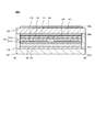
- FIG. 4A is a cross-sectional view of the liquid crystal panel 110.
- the liquid crystal panel 110 has a liquid crystal element 140 provided between the first substrate 101 and the second substrate 102. Further, the element layer 111 and the pixel electrode 141 are provided on the first surface 101a of the first substrate 101, and the color filter layer 112 and the common electrode 142 are provided on the second surface 102b of the second substrate 102. .. A guest host liquid crystal layer 113 is provided between the pixel electrode 141 and the common electrode 142. The first substrate 101 and the second substrate 102 are adhered to each other by an adhesive 115.
- the liquid crystal panel 110 may be formed by using a known method, and thus detailed description thereof will be omitted.
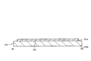
- FIG. 4B is a diagram illustrating a step of forming the first electrode 121 on the second surface 101b of the first substrate 101.
- the oxide conductive layer 121a is formed on the second surface 101b of the first substrate 101.
- the oxide conductive layer 121a By forming the oxide conductive layer 121a so that the sheet resistance is 5 ⁇ / ⁇ , unevenness of the voltage supplied to the oxide conductive layer 121a can be reduced.
- a metal conductive film is formed on the oxide conductive layer 121a on the oxide conductive layer 121a, and a metal conductive layer 121b having a plurality of openings is formed by a photolithography step.
- the wiring width forming the pattern having the plurality of openings is processed so as to be, for example, 1 ⁇ m or more and 10 ⁇ m or less.
- the first electrode 121 can be formed by forming the oxide conductive layer 121a and the metal conductive layer 121b having a plurality of openings.
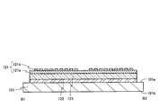
- FIG. 5A is a diagram illustrating a step of forming the light emitting layer 123 on the first electrode 121.
- a light emitting material is applied onto the first electrode 121 using a spin coater or a roll coater. Further, the light emitting material may be applied onto the first electrode 121 by using flexographic printing, offset printing, lift-off, inkjet, or the like. When flexographic printing, offset printing, lift-off, inkjet, or the like is used, the light emitting layer 123 can be patterned.
- Luminescent materials include luminescent polymers, ionic liquids, and organic solvents. Examples of the luminescent polymer include various ⁇ -conjugated polymers.
- the ionic liquid is a substance that maintains a liquid state at room temperature even though it is an ionic species.
- a phosnium-based material may be used, but other raw materials may be used.
- an organic solvent an ionic liquid and a luminescent polymer are efficiently mixed and used to secure an appropriate viscosity for coating on the first electrode 121.
- the organic solvent for example, it is preferable to use at least one selected from the group consisting of toluene, benzene, tetrahydrofuran, carbon disulfide, dimethyl chloride, chlorobenzene and chloroform.
- the organic solvent only one of these compounds or a combination of two or more of these compounds can be used.
- the annealing temperature is preferably a temperature at which the light emitting material does not deteriorate, for example, 120 ° C. or lower. Annealing may be performed in the air or in vacuum. By annealing, the organic solvent contained in the light emitting material is evaporated to form a light emitting layer 123 having a light emitting polymer and an ionic liquid.
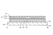
- FIG. 5B is a diagram illustrating a step of forming the second electrode 122 on the light emitting layer 123.
- the second electrode 122 is formed of aluminum by a sputtering method or a thin film deposition method.
- the second electrode 122 is formed on substantially the entire surface of the light emitting layer 123.
- the second electrode 122 is formed by a vapor deposition method using a metal mask. After the formation of the second electrode 122, the organic solvent of the light emitting layer 123 may be removed by further annealing. By the above steps, the electrochemical light emitting cell 120 can be formed.
- FIG. 6A is a diagram illustrating a step of forming the protective layer 124 on the second electrode 122.
- the protective layer 124 for example, a silicon nitride film or a silicon nitride film is formed by a sputtering method.
- FIG. 6B is a diagram illustrating a step of bonding the polarizing plate 114 on the first surface 102a of the second substrate 102.
- the polarization axes of the polarizing plate 114 are attached so as to be orthogonal to the axes of the liquid crystal molecules and the dye when no voltage is applied between the pixel electrode 141 and the common electrode 142.
- the display device 100 according to the embodiment of the present invention can be manufactured.
- the protective layer 124 preferably covers the side surfaces of the first electrode 121, the light emitting layer 123, and the second electrode 122. As a result, it is possible to prevent moisture from entering the inside of the electrochemical light emitting cell 120, so that deterioration of the electrochemical light emitting cell 120 can be suppressed.
- the electrochemical light emitting cell 120 can be formed by using the manufacturing line of the liquid crystal panel 110.
- An example of a surface-emitting lighting device that functions as a backlight is a lighting device that uses an organic EL.
- the light emitting layer provided between a pair of electrodes has a number of organic layers. It needs to be vapor-deposited and the manufacturing process is complicated.
- the manufacturing process is simple because the light-emitting layer 123 may be coated with an organic solvent containing a light-emitting polymer and an ionic liquid and then dried. Thereby, the productivity of the display device 100 can be improved.
- a plurality of display devices 100 can be manufactured at one time by using a large format substrate.
- the plurality of display devices 100 may be individually separated.
- the polarizing plate 114 may be attached onto the first surface 101a of the second substrate 102.
- FIG. 8 is a developed view of the display device 100A according to the embodiment of the present invention
- FIG. 9 is a cross-sectional view when the display device 100A shown in FIG. 8 is cut along the B1-B2 line.
- FIG. 10 is an enlarged cross-sectional view of a part of the display device 100A shown in FIG.
- the display device 100A shown in FIGS. 8 to 10 includes a liquid crystal panel 110A including an electrochemical light emitting cell 120A, and a polarizing plate 114.
- the electrochemical light emitting cell 120A functions as a backlight of the liquid crystal panel 110A.
- the electrochemical light emitting cell 120A is provided between the first substrate 101 and the second substrate 102.
- An electrochemical light emitting cell 120A is provided on the first surface 101a of the first substrate 101.
- the second electrode 122 is provided on the first surface 101a of the first substrate 101.
- the second electrode 122 is a reflective metal conductive layer.
- the first electrode 121 is provided with an oxide conductive layer 121a on a surface in contact with the light emitting layer 123, and a metal conductive layer 121b having a plurality of openings is provided on the oxide conductive layer 121a.
- the stacking order of the oxide conductive layer 121a and the metal conductive layer 121b is not particularly limited, and the metal conductive layer 121b is provided on the light emitting layer 123, and the oxide conductive layer 121a is provided on the metal conductive layer 121b. There may be.
- a color filter layer 112 is provided on the first electrode 121 of the electrochemical light emitting cell 120A.
- the color filter layer 112 includes, for example, at least a red color filter 112a, a green color filter 112b, a blue color filter 112c, and a black matrix 112d.
- an overcoat layer may be provided on the surface of the color filter 112a in contact with the guest host liquid crystal layer 113.
- an alignment film is provided on the surface of the color filter layer 112 or the overcoat layer in contact with the guest host liquid crystal layer 113.
- a color filter layer 112 may be provided in contact with the first electrode 121, or a color filter (not shown) via an insulating film made of an organic material or an inorganic material on the first electrode 121.
- the layer 112 may be provided.
- an organic resin is used as the insulating film, the surface can be flattened.
- a polarizing plate 114 is provided on the first surface 102a of the second substrate 102, and an element layer 111 is provided on the second surface 102b.
- the structure of the element layer 111 provided on the second surface 102b is the same as the structure of the element layer 111 described in the first embodiment.
- the pixel electrode 141 and the common electrode 142 preferably have translucency.
- a guest host liquid crystal layer 113 is provided between the color filter layer 112 of the first substrate 101 and the element layer 111 of the second substrate 102.
- the thickness of the electrochemical light emitting cell 120 is the total thickness of the first electrode 121, the light emitting layer 123, and the second electrode 122, and is 740 nm to 1050 nm.
- the thickness of the polarizing plate 114 is 50 ⁇ m to 100 ⁇ m. Therefore, the thickness of the electrochemical light emitting cell 120 can be made smaller than the thickness of the polarizing plate 114.
- the electrochemical light emitting cell 120A is provided between the first substrate 101 and the second substrate 102. Therefore, the light emitted from the electrochemical light emitting cell 120A passes through the color filter layer 112 and the element layer 111 and is taken out to the first surface 101a side of the second substrate 102. Further, since the electrochemical light emitting cell 120A is sealed by the first substrate 101, the second substrate 102, and the adhesive 115, it is possible to prevent the electrochemical light emitting cell 120A from being deteriorated by moisture or the like that has entered from the outside.
- FIG. 11A is a diagram illustrating a process of forming the element layer 111, the adhesive 115, and the guest host liquid crystal layer 113 on the second substrate 102. Since the element layer 111 may be formed by using a known method, detailed description thereof will be omitted. An alignment film is formed on the element layer 111. The alignment treatment for the alignment film is preferably performed by a photoalignment method. Further, after the element layer 111 is formed, the adhesive 115 is formed on the first substrate 101 so as to surround the element layer 111. Next, the guest host liquid crystal is dropped onto the region surrounded by the adhesive 115 to form the guest host liquid crystal layer 113.
- FIG. 11B is a diagram illustrating a step of forming the second electrode 122 on the first surface 101a of the first substrate 101.
- the second electrode 122 is formed of aluminum by a sputtering method or a thin film deposition method.
- the second electrode 122 is formed on substantially the entire surface of the first substrate 101 by using the metal conductive layer.
- FIG. 12A is a diagram illustrating a step of forming the light emitting layer 123 on the second electrode 122.
- the description of FIG. 5A may be referred to, and detailed description thereof will be omitted.
- FIG. 12B is a diagram illustrating a step of forming the first electrode 121 on the light emitting layer 123.
- a method of forming the oxide conductive layer 121a on the light emitting layer 123 and then forming the metal conductive layer 121b as the first electrode 121 will be described.
- the oxide conductive layer 121a and the metal conductive layer 121b are formed by a sputtering method or a vapor deposition method.
- the oxide conductive layer 121a is formed on substantially the entire surface of the light emitting layer 123.
- the oxide conductive layer 121a and the metal conductive layer 121b are formed on the light emitting layer 123, it is difficult to process the conductive film by performing a photolithography step on the light emitting layer 123. Therefore, when the oxide conductive layer 121a and the metal conductive layer 121b are formed on the light emitting layer 123, it is preferable to form them by a method that does not require a photolithography step.
- the oxide conductive layer 121a is formed by a vapor deposition method using a metal mask. After that, it is preferable to form the metal conductive layer 121b having a plurality of openings by using an inkjet method.
- the oxide conductive layer 121a may be formed after forming the metal conductive layer 121b on the light emitting layer 123 as the first electrode 121.
- FIG. 13A is a diagram illustrating a step of forming the color filter layer 112 on the first electrode 121.
- the color filters 112a to 112c may be formed in the openings of the black matrix 112d after the black matrix 112d is formed as the color filter layer 112.
- An insulating film may be formed on the first electrode 121 before the color filter layer 112 is formed.
- the common electrode 142 is formed.
- An overcoat layer may be formed between the color filter layer 112 and the common electrode 142.
- an alignment film is formed on the common electrode 142. The alignment treatment for the alignment film is preferably performed by a photoalignment method.
- FIG. 13B is a diagram illustrating a process of bonding the first substrate 101 and the second substrate 102.
- the surface of the first substrate 101 on which the guest host liquid crystal layer 113 is formed and the surface of the second substrate 102 on which the color filter layer 112 is formed are opposed to each other and bonded to each other.
- the bonding of the first substrate 101 and the second substrate 102 may be performed in the atmosphere or in a vacuum.
- the polarizing plate 114 is attached to the first surface 102a of the second substrate 102.
- the description of FIG. 6B may be referred to, and detailed description thereof will be omitted.
- the display device 100A according to the embodiment of the present invention can be manufactured.
- the present invention is not limited to this. It is also possible to manufacture a plurality of display devices 100A at one time using a large format substrate. In this case, the first substrate 101 and the second substrate 102 may be adhered to each other by the adhesive material 115, and then individualized for each of the plurality of display devices 100. After that, the polarizing plate 114 may be attached onto the second substrate 102.
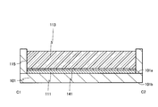
- FIG. 14 is a developed view of the display device 100B according to the embodiment of the present invention
- FIG. 15 is a cross-sectional view when the display device 100B shown in FIG. 14 is cut along the line C1-C2.
- FIG. 16 is an enlarged cross-sectional view of a part of the display device 100B shown in FIG.
- the display device 100B shown in FIGS. 14 to 16 includes a liquid crystal panel 110B including an electrochemical light emitting cell 120B, and a polarizing plate 114.
- the electrochemical light emitting cell 120B functions as a front light of the liquid crystal panel 110B.
- the electrochemical light emitting cell 120B is provided between the first substrate 101 and the second substrate 102.
- the difference from the display device 100A shown in the second embodiment is that the first electrode 121, the light emitting layer 123, and the second electrode 122 of the electrochemical light emitting cell 120B are patterned.
- the electrochemical light emitting cell 120B has a plurality of openings, and the first electrode 121, the light emitting layer 123, and the second electrode 122 are provided at positions overlapping with the black matrix 112d of the color filter layer 112. ing.
- an insulating layer 125 is provided on the black matrix 112d via a common electrode 142.
- the insulating layer 125 is patterned in the same shape as the first electrode 121, the light emitting layer 123, and the second electrode 122.
- the common electrode 142 is insulated from the second electrode 122 by the insulating layer 125.
- the shape of the plurality of openings of the electrochemical light emitting cell 120B is formed so as to surround each sub-pixel of RGB, for example.
- FIG. 17 is a plan view of the color filter layer 112, the first electrode 121, and the second electrode 122.
- Color filters 112a to 112c are provided in the openings of the black matrix 112d.
- the first electrode 121 is formed of an oxide conductive layer 121a and a metal conductive layer 121b having a plurality of openings. Further, the light emitting layer 123 has a plurality of openings. Further, the second electrode 122 is formed of a metal conductive layer having a plurality of openings.
- the first electrode 121, the light emitting layer 123, and the second electrode 122 are provided on the black matrix 112d.
- FIG. 17 shows an example in which the openings of the first electrode 121, the light emitting layer 123, and the second electrode 122 are provided in a grid pattern so as to surround each of the RGB sub-pixels.
- the embodiment is not limited to this.
- the openings of the first electrode 121 and the second electrode 122 may be provided in a grid pattern so as to surround the RGB pixels, or may be provided in a grid pattern so as to surround two or more RGB pixels. You may be.
- the size of the opening of the first electrode 121 and the size of the opening of the second electrode 122 may be different.
- the first electrode 121 may be provided in a grid pattern so as to surround each of the RGB sub-pixels
- the second electrode 122 may be provided in a grid pattern so as to surround the RGB pixels.
- the size of the opening of the oxide conductive layer 121a and the size of the opening of the metal conductive layer 121b may be different.
- the oxide conductive layer 121a may be provided in a grid pattern so as to surround each of the RGB sub-pixels
- the metal conductive layer 121b may be provided in a grid pattern so as to surround the RGB pixels.
- the first electrode 121 is provided on the black matrix 112d. Therefore, the first electrode 121 may be configured to provide only the metal conductive layer 121b without providing the oxide conductive layer 121a. Further, the first electrode 121 may be provided in contact with the color filter layer 112, and the second electrode 122 may be provided in contact with the light emitting layer 123. In this case as well, the first electrode 121 may be configured to provide only the metal conductive layer 121b without providing the oxide conductive layer 121a.
- the point that the element layer 111 is provided on the first surface 101a of the first substrate 101 is the same as that of the first embodiment.
- the pixel electrode 141 is formed of a reflective metal conductive layer.
- the pixel electrode 141 is superimposed on the color filter.
- the second electrode 122 is formed of a conductive metal conductive layer.
- the light emitted from the light emitting layer 123 of the electrochemical light emitting cell 120B is directed toward the element layer 111 by the second electrode 122. After that, the light is reflected by the pixel electrode 141.
- the reflected light is emitted to the second substrate 102 side through the opening formed in the electrochemical light emitting cell 120B and the opening of the black matrix 112d.
- the surface of the pixel electrode 141 formed of the conductive layer having the reflectivity may have an uneven shape.
- the thickness of the electrochemical light emitting cell 120 is the total thickness of the first electrode 121, the light emitting layer 123, and the second electrode 122, and is 740 nm to 1050 nm.
- the thickness of the polarizing plate 114 is 50 ⁇ m to 100 ⁇ m. Therefore, the thickness of the electrochemical light emitting cell 120 can be made smaller than the thickness of the polarizing plate 114.
- FIG. 18A is a diagram illustrating a step of forming the element layer 111, the adhesive 115, and the guest host liquid crystal layer 113 on the first surface 101a of the first substrate 101. Since the element layer 111 may be formed by using a known method, detailed description thereof will be omitted.
- the pixel electrode 141 is formed on the element layer 111. After that, an alignment film is formed on the pixel electrode 141. The alignment treatment for the alignment film is preferably performed by a photoalignment method. Further, after the element layer 111 is formed, the adhesive 115 is formed on the first substrate 101 so as to surround the element layer 111. Next, the guest host liquid crystal is dropped onto the region surrounded by the adhesive 115 to form the guest host liquid crystal layer 113.
- FIG. 18B is a diagram illustrating a step of forming the color filter layer 112 on the second surface 102b of the second substrate 102.
- the color filters 112a to 112c may be formed in the openings of the black matrix 112d after the black matrix 112d is formed as the color filter layer 112.
- the common electrode 142 is formed after the color filter layer 112 is formed.
- An overcoat layer may be formed between the color filter layer 112 and the common electrode 142.
- FIG. 19A is a diagram illustrating a step of forming an insulating layer 125 having a plurality of openings and a second electrode 122 on the color filter layer 112.
- the insulating layer 125 is formed by applying and curing an insulating material so as to have a plurality of openings by using flexographic printing, offset printing, lift-off, inkjet, or the like.
- the second electrode 122 is formed of aluminum by a vapor deposition method using a metal mask.
- the second electrode 122 is formed so as to overlap with the black matrix 112d. As a result, the second electrode 122 is formed in a grid pattern having a plurality of openings.
- FIG. 19B is a diagram illustrating a step of forming a light emitting layer 123 having a plurality of openings on the second electrode 122.
- a light emitting material is applied onto the second electrode 122 by using flexographic printing, offset printing, lift-off, inkjet, or the like. As a result, the light emitting material is formed so as to overlap with the second electrode 122.
- the light emitting material coated on the second electrode 122 is annealed. By annealing, the organic solvent contained in the light emitting material is evaporated to form a light emitting layer 123 having a light emitting polymer and an ionic liquid. As a result, the light emitting layer 123 is formed in a grid pattern having a plurality of openings.
- FIG. 20A is a diagram illustrating a step of forming a first electrode 121 having a plurality of openings on the light emitting layer 123.
- an oxide conductive layer 121a having a plurality of openings is formed on the light emitting layer 123.
- the metal conductive layer 121b having a plurality of openings is formed.
- the oxide conductive layer 121a and the metal conductive layer 121b are preferably formed by a method that does not require a photolithography step. Therefore, the oxide conductive layer 121a and the metal conductive layer 121b are formed by a vapor deposition method using a metal mask.
- the first electrode 121 forms the first electrode 121 having a plurality of openings.
- an alignment film is formed on the surfaces of the common electrode 142, the first electrode 121, the light emitting layer 123, and the second electrode 122 in contact with the guest host liquid crystal layer 113.
- FIG. 20B is a diagram illustrating a process of bonding the first substrate 101 and the second substrate 102.
- the surface of the first substrate 101 on which the guest host liquid crystal layer 113 is formed and the surface of the second substrate 102 on which the first electrode 121 is formed are opposed to each other and bonded to each other.
- the bonding of the first substrate 101 and the second substrate 102 may be performed in the atmosphere or in a vacuum.
- the polarizing plate 114 is attached to the first surface 102a of the second substrate 102.
- the description of FIG. 6B may be referred to, and detailed description thereof will be omitted.
- the display device 100B according to the embodiment of the present invention can be manufactured.
- the present invention is not limited to this. It is also possible to manufacture a plurality of display devices 100A at one time using a large format substrate. In this case, the first substrate 101 and the second substrate 102 may be adhered to each other by the adhesive material 115, and then individualized for each of the plurality of display devices 100. After that, the polarizing plate 114 may be attached onto the second substrate 102.
- the common electrode 142 and the second electrode 122 may be insulated by partially removing the common electrode 142 in a region overlapping the black matrix 112d. Further, the common electrode 142 and the second electrode 122 may be insulated by partially removing the common electrode 142 in the region overlapping the black matrix 122d and further providing the insulating layer 125.
- 100, 100A, 100B Display device, 101: 1st substrate, 101a: 1st surface, 101b: 2nd surface, 102: 2nd substrate, 102a: 1st surface, 102b: 2nd surface, 110: Liquid crystal panel, 110A: Liquid crystal panel, 110B: Liquid crystal panel, 111: Element layer, 112: Color filter layer, 112a: Color filter, 112b: Color filter, 112c: Color filter, 112d: Black matrix, 113: Guest host liquid crystal layer, 114: Liquid crystal display, 115: Adhesive, 120: Electrochemical light emitting cell, 120A: Electrochemical light emitting cell, 120B: Electrochemical light emitting cell, 121: First electrode, 121a: Oxide conductive layer, 121b: Metal conductive layer, 122: Second electrode, 122a: color filter, 122b: color filter, 122c: color filter, 122d: black matrix, 123: light emitting layer, 124: protective layer, 130:
Landscapes
- Physics & Mathematics (AREA)
- Nonlinear Science (AREA)
- General Physics & Mathematics (AREA)
- Engineering & Computer Science (AREA)
- Chemical & Material Sciences (AREA)
- General Engineering & Computer Science (AREA)
- Crystallography & Structural Chemistry (AREA)
- Optics & Photonics (AREA)
- Liquid Crystal (AREA)
- Mathematical Physics (AREA)
- Electromagnetism (AREA)
- Electrochemistry (AREA)
- Theoretical Computer Science (AREA)
- Electroluminescent Light Sources (AREA)
- Planar Illumination Modules (AREA)
- Devices For Indicating Variable Information By Combining Individual Elements (AREA)
Abstract
表示装置は、第1面及び第1面と反対側の第2面を有する第1基板と、第3面及び第3面と反対側の第4面を有する第2基板と、第1基板の第1面と第2基板の第4面との間に設けられたゲストホスト液晶層と、第1基板の第2面に設けられた第1電極と、発光ポリマー及びイオン液体を含み、第1電極の第1基板とは反対側の面に設けられた発光層と、発光層を間に挟んで、第1電極と対向して設けられた第2電極と、第2基板の第3面に設けられた偏光板と、を有する。
Description
本発明の一実施形態は、電気化学発光セル(LEC:Light-emitting Electrochemical Cell)を有する表示装置及び表示装置の製造方法に関する。
表示装置の一例として、液晶表示装置や有機EL(Electroluminescence:EL)表示装置等がある。液晶表示装置は、基板上に形成された複数の画素の各々に液晶素子を有している。液晶素子は、一対の電極間に液晶層を有しており、一対の電極間に電圧を印加することで駆動される。また、有機EL表示装置は、基板上に形成された複数の画素の各々に発光素子を有している。発光素子は、一対の電極間に、電界発光性を示す有機化合物を含む有機層を有しており、一対の電極間に電流を流すことにより駆動される。
液晶表示装置用のバックライトは、液晶表示装置の一端部と重畳する位置に複数のLEDのマウント部を有するエッジライト方式が主流である。これら複数のLEDによる点状の光を、導光板、拡散フィルム、及び反射フィルムによって、面状の光に換えて液晶表示装置に射出している。
従来のバックライトでは、各々が数十μm~数百μm程度の光学フィルムを積層して構成されている。液晶パネルには、表示面側と表示面とは反対側の面にそれぞれ偏光板が設けられている。そして、液晶表示装置では、バックライト上に液晶パネルを積層して構成されている。そのため、バックライトの厚み及び液晶パネルとの厚みにより、これらの総厚は、有機EL表示装置の総厚よりも厚くなってしまうという問題がある。
上記の問題に鑑み、本発明の一実施形態では、表示装置の総厚を低減することを目的の一つとする。
本発明の一実施形態に係る表示装置は、第1面及び第1面と反対側の第2面を有する第1基板と、第3面及び第3面と反対側の第4面を有する第2基板と、第1基板の第1面と第2基板の第4面との間に設けられたゲストホスト液晶層と、第1基板の第2面に設けられた第1電極と、発光ポリマー及びイオン液体を含み、第1電極の第1基板とは反対側の面に設けられた発光層と、発光層を間に挟んで、第1電極と対向して設けられた第2電極と、第2基板の第3面に設けられた偏光板と、を有する。
本発明の一実施形態に係る表示装置は、第1面及び第1面と反対側の第2面を有する第1基板と、第3面及び第3面と反対側の第4面を有する第2基板と、第1基板の第1面上に設けられた第2電極と、発光ポリマー及びイオン液体を含み、第2電極上に設けられた発光層と、発光層上に設けられた第1電極と、第1電極と、第2基板の第4面との間に設けられたゲストホスト液晶層と、第2基板の第3面上に設けられた偏光板と、を有する。
本発明の一実施形態に係る表示装置は、第1面及び第1面と反対側の第2面を有する第1基板と、第3面及び第3面と反対側の第4面を有する第2基板と、第1基板の第1面上に設けられたゲストホスト液晶と、第2基板の第4面に設けられたブラックマトリクス及びカラーフィルタと、ブラックマトリクス上に設けられた第2電極と、発光ポリマー及びイオン液体を含み、第2電極上に設けられた発光層と、発光層上に設けられた第1電極と、第2基板の第3面に設けられた偏光板と、を有する。
以下、本発明の実施の形態を、図面等を参照しながら説明する。但し、本発明は多くの異なる態様で実施することが可能であり、以下に例示する実施の形態の記載内容に限定して解釈されるものではない。図面は説明をより明確にするため、実際の態様に比べ、各部の幅、厚さ、形状等について模式的に表される場合があるが、あくまで一例であって、本発明の解釈を限定するものではない。また、本明細書と各図において、既出の図に関して前述したものと同様の要素には、同一の符号(又は数字の後にA、Bなどを付した符号)を付して、詳細な説明を適宜省略することがある。さらに各要素に対する「第1」、「第2」と付記された文字は、各要素を区別するために用いられる便宜的な標識であり、特段の説明がない限りそれ以上の意味を有さない。
本明細書において、ある部材又は領域が他の部材又は領域の「上に(又は下に)」あるとする場合、特段の限定がない限りこれは他の部材又は領域の直上(又は直下)にある場合のみでなく他の部材又は領域の上方(又は下方)にある場合を含み、すなわち、他の部材又は領域の上方(又は下方)において間に別の構成要素が含まれている場合も含む。なお、以下の説明では、特に断りのない限り、断面視において、ベース部材に対してタッチセンサが設けられる側を「上」又は「上方」といい、「上」又は「上方」から見た面を「上面」又は「上面側」というものとし、その逆を「下」、「下方」、「下面」又は「下面側」というものとする。
(第1実施形態)
本発明の一実施形態に係る表示装置100について、図1乃至図6を参照して説明する。
本発明の一実施形態に係る表示装置100について、図1乃至図6を参照して説明する。
<表示装置の構成>
まず、本発明の一実施形態に係る表示装置100の構成について図1乃至図3を参照して説明する。図1は、本発明の一実施形態に係る表示装置の展開図であり、図2は、図1に示す表示装置100をA1-A2線に沿って切断したときの断面図である。また、図3は、図2に示す表示装置100の一部を拡大した断面図である。図1乃至図3に示す表示装置100は、液晶パネル110、電気化学発光セル120、及び偏光板114、を有する。電気化学発光セル120は、液晶パネル110のバックライトとして機能する。
まず、本発明の一実施形態に係る表示装置100の構成について図1乃至図3を参照して説明する。図1は、本発明の一実施形態に係る表示装置の展開図であり、図2は、図1に示す表示装置100をA1-A2線に沿って切断したときの断面図である。また、図3は、図2に示す表示装置100の一部を拡大した断面図である。図1乃至図3に示す表示装置100は、液晶パネル110、電気化学発光セル120、及び偏光板114、を有する。電気化学発光セル120は、液晶パネル110のバックライトとして機能する。
本発明の一実施形態に係る表示装置100において、第2基板102に偏光板114が設けられている面が、表示装置100の表示面側であるとして説明する。以降の説明において、第2基板102の偏光板114が設けられている面を、第1面102aとし、反対側の面を第2面102bとして説明する。また、第1基板101においても同様に、表示面側を第1面101aとし、反対側の面を第2面101bとして説明する。
電気化学発光セル120は、第1基板101の第2面101b側に設けられる。電気化学発光セル120は、第1電極121と、第2電極122との間に、発光ポリマー及びイオン液体を含む発光層123を挟んだ構成を有する。発光層123には、電子とイオンの双方が含まれており、第1電極121と第2電極122との間に電圧を印加することで、自発的にp-i-n結合を形成することで発光層123が発光する。なお、イオン液体とは、室温で液体の有機塩をいう。
第1電極121は、酸化物導電層121a及び金属導電層121bを有する。酸化物導電層121aは、透光性を有する導電層であり、第1基板101の第2面101b側のほぼ全面に形成される。酸化物導電層121aは、金属導電層121bよりも抵抗が高い。そのため、酸化物導電層121aが第1基板101の第2面101bのほぼ全面に設けられる場合、第1電極121の一端に電位が供給されると、他端において電位の減衰が生じて、発光輝度にむらが生じてしまう。そこで、酸化物導電層121aに重畳して、複数の開口部を有する金属導電層121bを設けることより、第1電極121の全体の抵抗を下げる。これにより、第1電極121の一端に供給された電位は、他端においても電位の減衰を抑制することができ、発光輝度のむらを抑制することができる。ここで、酸化物導電層121aの膜厚は、例えば、約75nm(50nm~100nm)であり、金属導電層121bの膜厚は、約600nm(550nm~650nm)である。また、第1電極121の総厚は、1μm未満であることが好ましい。
金属導電層121bに設けられた複数の開口部を有するパターンは、例えば、視認されない程度に配線を細くした格子状、又はメッシュ状である。格子状とは、具体的に、第1方向D1に延びた複数の配線と第2方向D2に延びた複数の配線とが直交に交差するパターンを有する構造である。また、メッシュ状とは、具体的に、複数の配線どうしが上記直行交差以外の角度で交差するパターンを有する構造である。この場合、例えばこれら複数の配線によって形成される開口部はひし形や平行四辺形状である。複数の開口部を有するパターンを構成する配線幅は、例えば、1μm以上10μm以下が好ましい。
第1電極121の酸化物導電層121aは第1基板101の第2面101bと接し、金属導電層121bは発光層123と接していてもよいし、金属導電層121bが第1基板101の第2面101bと接し、酸化物導電層121aが発光層123と接していてもよい。酸化物導電層121aとして、例えば、酸化インジウムスズ(Indium Tin Oxide;ITO)、酸化インジウム亜鉛(Indium Zinc Oxide;IZO)を用いる。また、透光性を有する導電層として、酸化物導電層121aに代えてMgAg薄膜を用いてもよい。金属導電層121bとして、例えば、チタン、アルミニウム、及びチタンを積層して用いる。
発光層123は、第1電極121のほぼ全面に形成され、発光ポリマー及びイオン液体を含む。電気化学発光セル120をバックライトとして使用する場合、発光層123の発光色は白色が好ましい。発光層123の膜厚は、約100nm(90nm~200nm)である。
第2電極122は金属導電層を用いて、発光層123のほぼ全面に形成される。第2電極122は、反射率が高い金属導電層を有する。反射率が高い金属層により、発光層123から発光した光を反射して、第1電極121を透過して、第2基板102から光を射出する。第2電極122として、例えば、アルミニウムを用いる。第2電極122の膜厚は、50nm~100nmである。
電気化学発光セル120の厚みは、第1電極121、発光層123、及び第2電極122の総厚となり、740nm~1050nmとなる。ここで、偏光板114の厚みは、50μm~100μmである。したがって、電気化学発光セル120の厚みは、偏光板114の厚みよりも小さくすることができる。
保護層124は、電気化学発光セル120の第2電極122のほぼ全面に形成される。保護層124は、窒化シリコン膜又は窒化アルミニウム膜を有することにより、水分の透過を抑制して、発光層123に水分が侵入することを抑制することができる。これにより、発光層123が水分によって劣化することを抑制することができる。また、保護層124は、第1電極121、発光層123、及び第2電極122の側面を覆うことが好ましい。保護層124の膜厚は、50nm~2000nmである。
本発明の一実施形態に係る表示装置100は、液晶パネル110のバックライトとして、第1電極121、発光層123、及び第2電極122で構成された電気化学発光セル120を設けている。電気化学発光セル120が有する第1電極121、発光層123、及び第2電極122のそれぞれは、数十nm~数百nm程度で形成することができる。したがって、従来の光学フィルムを用いたバックライトと比較して、バックライトの厚みを小さくすることができる。
液晶パネル110は、第1基板101と、第1基板101に対向する第2基板102と、第1基板101と第2基板102との間に設けられた液晶素子140と、を少なくとも有する。液晶素子140は、画素電極141と、ゲストホスト液晶層113と、共通電極142と、を有する。また、第1基板101の第1面101aには、素子層111及び画素電極141が設けられ、第2基板102の第2面102bには、カラーフィルタ層112及び共通電極142が設けられている。液晶パネル110の構成について、図3を参照して説明する。
第1基板101及び第2基板102として、例えば、ガラス基板、プラスチック基板を用いる。プラスチック基板として、例えば、アクリル、ポリイミド、ポリエチレンテレフタレート、ポリエチレンナフタレート等の有機樹脂を用いる。また、第1基板101及び第2基板102として、可撓性を有するプラスチック基板を用いることにより、折り曲げたり、湾曲させたりすることが可能な表示装置100を形成することができる。
ゲストホスト液晶層113は、液晶分子及び色素を有する。液晶分子(ホスト液晶)は、誘電率異方性が負の液晶分子である。色素(ゲスト色素)は、例えば、黒色色素である。色素は、液晶分子に沿って配向する。画素電極141と共通電極142との間に発生する電界により、液晶分子の配向の変化に応じて、色素の配向も変化する。
第1基板101の第1面101aに、素子層111が設けられている。素子層111は、例えば、トランジスタ130、及びトランジスタ130上に設けられた絶縁層を少なくとも含む。トランジスタ130は、第1基板101の第1面101aに下地膜131を介して設けられていてもよい。また、トランジスタ130は、半導体層132、ゲート絶縁膜133、ゲート電極134を少なくとも有する。ゲート電極134上には、層間絶縁膜135が設けられており、層間絶縁膜135上には、ソース電極又はドレイン電極136が設けられている。ソース電極又はドレイン電極136は、層間絶縁膜135に形成された開口部を介して半導体層132と接続されている。ソース電極又はドレイン電極136上には、平坦化膜137が設けられている。図3では、トランジスタ130としてトップゲート構造で示しているが、ボトムゲート構造であってもよい。
平坦化膜137上には、画素電極141が設けられており、画素電極141上にはゲストホスト液晶層113が設けられている。画素電極141は、平坦化膜137に設けられた開口部を介して、ソース電極又はドレイン電極136と接続されている。画素電極141は、透光性を有することが好ましい。なお、図示しないが、画素電極141のゲストホスト液晶層113と接する面には、配向膜が設けられている。
第2基板102の第2面102bには、カラーフィルタ層112が設けられている。カラーフィルタ層112は、例えば、赤色のカラーフィルタ112a、緑色のカラーフィルタ112b、青色のカラーフィルタ112c、及びブラックマトリクス112dを少なくとも含む。隣り合うカラーフィルタは、ブラックマトリクス112d上で重なりあってもよい。カラーフィルタ層112のゲストホスト液晶層113と接する面には、共通電極142が設けられている。共通電極142は、透光性を有することが好ましい。なお、カラーフィルタ層112と共通電極142との間には、オーバーコート層が設けられていてもよい。また、図示しないが、共通電極142のゲストホスト液晶層113と接する面には、配向膜が設けられている。画素電極141と、ゲストホスト液晶層113と、共通電極142とにより、液晶素子140が構成される。
接着材115は、第1基板101及び第2基板102の周縁部を囲むように設けられている。第1基板101と第2基板102とは、接着材115によって貼り合わされている。
第2基板102の第1面101aには、偏光板114が設けられている。偏光板114の偏光軸は、画素電極141と共通電極142との間に電圧が印加されていない場合に、ゲストホスト液晶層113の液晶分子及び色素の軸と直交するように設けられる。このとき、電気化学発光セル120から射出された光は、偏光板114の偏光軸により吸収されるため、偏光板114を通過しない。また、偏光板114の偏光軸は、画素電極141と共通電極142との間に電圧が印加されている場合に、ゲストホスト液晶層113の液晶分子及び色素の軸と平行となる。このとき、電気化学発光セル120から射出された光は、偏光板114の偏光軸に吸収されず、偏光板114を通過する。
本発明の一実施形態に係る表示装置100では、第1基板101の第2面101bに、電気化学発光セル120を設けている。したがって、電気化学発光セル120から射出された光は、素子層111及びカラーフィルタ層112を通過して、第2基板102の第1面101a側へ取り出される。
本発明の一実施形態に係る液晶パネル110では、ゲストホスト液晶層113を用いているため、液晶パネル110と電気化学発光セル120との間において、偏光板114が不要となる。これにより、表示装置100の液晶パネル110及びバックライトとして機能する電気化学発光セル120の総厚を小さくすることができる。
<表示装置の製造方法>
次に、本発明の一実施形態に係る表示装置100の製造方法について、図4乃至図6を参照して説明する。
次に、本発明の一実施形態に係る表示装置100の製造方法について、図4乃至図6を参照して説明する。
図4Aは、液晶パネル110の断面図である。液晶パネル110は、第1基板101と、第2基板102との間に設けられた液晶素子140を有する。また、第1基板101の第1面101aには、素子層111及び画素電極141が設けられ、第2基板102の第2面102bには、カラーフィルタ層112及び共通電極142が設けられている。画素電極141と共通電極142との間にゲストホスト液晶層113が設けられている。第1基板101と、第2基板102とは、接着材115によって接着されている。本実施形態では、液晶パネル110は、既知の方法を用いて形成すればよいため、詳細な説明は省略する。
図4Bは、第1基板101の第2面101b上に、第1電極121を形成する工程を説明する図である。まず、第1基板101の第2面101b上に、酸化物導電層121aを形成する。酸化物導電層121aは、シート抵抗が5Ω/□となるように形成することで、酸化物導電層121aに供給される電圧のムラを低減することができる。次に、酸化物導電層121a上に、酸化物導電層121a上に金属導電膜を形成し、フォトリソグラフィ工程により、複数の開口部を有する金属導電層121bを形成する。また、複数の開口部を有するパターンを構成する配線幅は、例えば、1μm以上10μm以下となるように加工することが好ましい。酸化物導電層121a及び複数の開口部を有する金属導電層121bを形成することにより、第1電極121を形成することができる。
図5Aは、第1電極121上に発光層123を形成する工程について説明する図である。まず、スピンコータ、ロールコータを用いて第1電極121上に発光材料を塗布する。また、フレキソ印刷、オフセット印刷、リフトオフ、インクジェットなどを用いて、第1電極121上に発光材料を塗布してもよい。フレキソ印刷、オフセット印刷、リフトオフ、インクジェットなどを用いる場合には、発光層123をパターン化することができる。発光材料は、発光ポリマー、イオン液体、及び有機溶剤を含む。発光ポリマーとして、各種のπ共役系ポリマーを挙げることができる。具体的には、パラフェニレンビニレン、フルオレン、1,4-フェニレン、チオフェン、ピロール、パラフェニレンスルフィド、ベンゾチアジアゾール、ビオチオフィン若しくはこれらに置換基を導入させた誘導体のポリマー又はこれらを含むコポリマー等を挙げることができる。また、イオン液体とは、イオン種でありながら常温において液体状態を維持する物質であり、一例としては、ホスニウム系を原料とするものが挙げられるが、他の原料を用いても構わない。有機溶媒として、イオン液体と発光ポリマーとを効率よく混合し、第1電極121上に塗布するための適度な粘度を確保するために用いる。有機溶媒として、例えば、トルエン、ベンゼン、テトラヒドロフラン、二硫化炭素、ジメチルクロライド、クロロベンゼン及びクロロホルムからなる群から選ばれる少なくとも1種を用いることが好ましい。この場合、有機溶媒として、これらの化合物の1種のみを、又は2種以上を組み合わせたもののみを用いることができる。
次に、第1電極121上に塗布した発光材料にアニールを行う。アニールの温度は、発光材料が劣化しない温度、例えば、120℃以下で行うことが好ましい。アニールは、大気中で行ってもよいし、真空中で行ってもよい。アニールにより、発光材料に含まれる有機溶剤を蒸発させることにより、発光ポリマー及びイオン液体を有する発光層123を形成する。
図5Bは、発光層123上に、第2電極122を形成する工程について説明する図である。第2電極122として、スパッタリング法又は蒸着法によりアルミニウムを用いて形成する。第2電極122は、発光層123のほぼ全面に形成される。発光層123上に、第2電極122を形成する場合、発光層123上において、フォトリソグラフィ工程を行って導電膜を加工ことは困難である。そのため、発光層123上に、第2電極122を形成する場合には、フォトリソグラフィ工程が不要な方法により形成することが好ましい。例えば、メタルマスクを用いて蒸着法により第2電極122を形成する。第2電極122の形成後に、さらにアニールを行うことで、発光層123の有機溶媒を除去してもよい。以上の工程により、電気化学発光セル120を形成することができる。
図6Aは、第2電極122上に保護層124を形成する工程を説明する図である。保護層124として、例えば、スパッタリング法により、窒化シリコン膜又は窒化シリコン膜を形成する。
図6Bは、第2基板102の第1面102a上に、偏光板114を貼り合わせる工程を説明する図である。偏光板114の偏光軸は、画素電極141と共通電極142との間に電圧が印加されていない場合に、液晶分子及び色素の軸とは直交するように貼り合わせる。
以上の工程により、本発明の一実施形態に係る表示装置100を製造することができる。
また、図7に示すように、保護層124は、第1電極121、発光層123、及び第2電極122の側面を覆うことが好ましい。これにより、電気化学発光セル120の内部に水分が侵入することを抑制することができるため、電気化学発光セル120が劣化することを抑制することができる。
本発明の一実施形態に係る表示装置100の製造方法では、電気化学発光セル120を、液晶パネル110の製造ラインを使用して形成することができる。
バックライトとして機能する面発光の照明装置として、有機ELを用いた照明装置が挙げられるが、有機ELを用いて照明装置では、一対の電極間に設けられる発光層は、何層もの有機層を蒸着する必要があり、製造工程が複雑である。これに対し、本実施形態で説明した電気化学発光セル120では、発光層123として、発光ポリマー及びイオン液体を含む有機溶媒を、塗布した後に乾燥すればよいので、製造工程が簡便である。これにより、表示装置100の生産性を向上させることができる。
本実施形態では、一つの基板に対して、一つの表示装置100を製造する場合について説明したが、本発明はこれに限定されない。大判基板を用いて、複数の表示装置100を一度に製造することもできる。この場合には、第1基板101上に複数の電気化学発光セル120を形成した後、複数の表示装置100毎に個片化すればよい。その後、第2基板102の第1面101a上に、偏光板114を貼り合わせればよい。
(第2実施形態)
本発明の一実施形態に係る表示装置100Aについて、図8乃至図12を参照して説明する。
本発明の一実施形態に係る表示装置100Aについて、図8乃至図12を参照して説明する。
<表示装置の構成>
まず、本発明の一実施形態に係る表示装置100Aの構成について図8乃至図10を参照して説明する。図8は、本発明の一実施形態に係る表示装置100Aの展開図であり、図9は、図8に示す表示装置100AをB1-B2線に沿って切断したときの断面図である。また、図10は、図9に示す表示装置100Aの一部を拡大した断面図である。図8乃至図10に示す表示装置100Aは、電気化学発光セル120Aを含む液晶パネル110A、及び偏光板114、を有する。電気化学発光セル120Aは、液晶パネル110Aのバックライトとして機能する。
まず、本発明の一実施形態に係る表示装置100Aの構成について図8乃至図10を参照して説明する。図8は、本発明の一実施形態に係る表示装置100Aの展開図であり、図9は、図8に示す表示装置100AをB1-B2線に沿って切断したときの断面図である。また、図10は、図9に示す表示装置100Aの一部を拡大した断面図である。図8乃至図10に示す表示装置100Aは、電気化学発光セル120Aを含む液晶パネル110A、及び偏光板114、を有する。電気化学発光セル120Aは、液晶パネル110Aのバックライトとして機能する。
本実施形態では、電気化学発光セル120Aは、第1基板101と第2基板102との間に設けられる。第1基板101の第1面101a上に、電気化学発光セル120Aが設けられる。
図9及び図10では、第1基板101の第1面101a上に、第2電極122が設けられる。第2電極122は、反射性を有する金属導電層である。第1電極121は、発光層123と接する面に、酸化物導電層121aが設けられ、酸化物導電層121a上に、複数の開口部を有する金属導電層121bが設けられている。酸化物導電層121aと金属導電層121bとの積層順は特に限定されず、発光層123上に、金属導電層121bが設けられ、金属導電層121b上に酸化物導電層121aが設けられる構成であってもよい。
電気化学発光セル120Aの第1電極121上に、カラーフィルタ層112が設けられる。カラーフィルタ層112は、例えば、赤色のカラーフィルタ112a、緑色のカラーフィルタ112b、青色のカラーフィルタ112c、及びブラックマトリクス112dを少なくとも含む。なお、図示しないが、カラーフィルタ112aのゲストホスト液晶層113と接する面には、オーバーコート層が設けられていてもよい。また、図示しないが、カラーフィルタ層112又はオーバーコート層のゲストホスト液晶層113と接する面には、配向膜が設けられている。
図10に示すように、第1電極121に接してカラーフィルタ層112が設けられていてもよいし、図示しないが第1電極121上に有機材料または無機材料の絶縁膜を介して、カラーフィルタ層112が設けられていてもよい。絶縁膜として、有機樹脂を用いる場合は、表面の平坦化を図ることができる。
第2基板102の第1面102aには、偏光板114が設けられ、第2面102bには、素子層111が設けられる。第2面102bに設けられる素子層111の構造は、第1実施形態で説明した素子層111の構造と同様である。画素電極141及び共通電極142は、透光性を有することが好ましい。第1基板101のカラーフィルタ層112と、第2基板102の素子層111との間には、ゲストホスト液晶層113が設けられる。
本発明の一実施形態に係る表示装置100Aにおいても、電気化学発光セル120の厚みは、第1電極121、発光層123、及び第2電極122の総厚となり、740nm~1050nmとなる。ここで、偏光板114の厚みは、50μm~100μmである。したがって、電気化学発光セル120の厚みは、偏光板114の厚みよりも小さくすることができる。
本発明の一実施形態に係る表示装置100Aでは、第1基板101と第2基板102との間に、電気化学発光セル120Aを設けている。したがって、電気化学発光セル120Aから射出された光は、カラーフィルタ層112及び素子層111を通過して、第2基板102の第1面101a側へ取り出される。また、第1基板101、第2基板102、及び接着材115によって封止されるため、電気化学発光セル120Aが、外部から侵入した水分などにより劣化することを抑制することができる。
<表示装置の製造方法>
次に、本発明の一実施形態に係る表示装置100Aの製造方法について、図11乃至図13を参照して説明する。
次に、本発明の一実施形態に係る表示装置100Aの製造方法について、図11乃至図13を参照して説明する。
図11Aは、第2基板102上に、素子層111、接着材115、及びゲストホスト液晶層113を形成する工程を説明する図である。素子層111は、既知の方法を用いて形成すればよいため、詳細な説明は省略する。なお、素子層111上には、配向膜を形成する。配向膜に対する配向処理は、光配向法により行うことが好ましい。また、素子層111を形成した後、第1基板101上に、素子層111を囲むように接着材115を形成する。次に、接着材115によって囲まれた領域に、ゲストホスト液晶を滴下して、ゲストホスト液晶層113を形成する。
図11Bは、第1基板101の第1面101aに、第2電極122を形成する工程を説明する図である。第2電極122として、スパッタリング法又は蒸着法によりアルミニウムを用いて形成する。第2電極122は、金属導電層を用いて、第1基板101のほぼ全面に形成される。第1基板101上に、第2電極122を形成する場合、第1実施形態における製造方法とは異なり、フォトリソグラフィ工程を行って、導電膜を加工することが可能である。
図12Aは、第2電極122上に発光層123を形成する工程について説明する図である。第2電極122上に、発光層123を形成する方法については、図5Aの説明を参照すればよいため、詳細な説明は省略する。
図12Bは、発光層123上に、第1電極121を形成する工程を説明する図である。本実施形態では、第1電極121として、発光層123上に、酸化物導電層121aを形成した後、金属導電層121bを形成する方法について説明する。酸化物導電層121a及び金属導電層121bとして、スパッタリング法又は蒸着法を用いて形成する。酸化物導電層121aは、発光層123のほぼ全面に形成される。発光層123上に、酸化物導電層121a及び金属導電層121bを形成する場合、発光層123において、フォトリソグラフィ工程を行って導電膜を加工することは困難である。そのため、発光層123上に、酸化物導電層121a及び金属導電層121bを形成する場合には、フォトリソグラフィ工程が不要な方法により形成することが好ましい。例えば、メタルマスクを用いて蒸着法により、酸化物導電層121aを形成する。その後、インクジェット法を用いて複数の開口部を有する金属導電層121bを形成することが好ましい。なお、図示はしないが、第1電極121として、発光層123上に、金属導電層121bを形成した後、酸化物導電層121aを形成してもよい。
図13Aは、第1電極121上に、カラーフィルタ層112を形成する工程を説明する図である。詳細な構成は図示しないが、カラーフィルタ層112として、ブラックマトリクス112dを形成した後、ブラックマトリクス112dの開口部に、カラーフィルタ112a~112cを形成すればよい。なお、カラーフィルタ層112を形成する前に、第1電極121上に絶縁膜を形成してもよい。カラーフィルタ層112の形成後に、共通電極142を形成する。なお、カラーフィルタ層112と共通電極142との間に、オーバーコート層を形成してもよい。また、共通電極142上に、配向膜を形成する。配向膜に対する配向処理は、光配向法により行うことが好ましい。
図13Bは、第1基板101と、第2基板102とを貼り合わせる工程を説明する図である。第1基板101のゲストホスト液晶層113が形成された面と、第2基板102のカラーフィルタ層112が形成された面と、を対向させて貼り合わせる。第1基板101と第2基板102との貼り合わせは、大気中で行ってもよいし、真空中で行ってもよい。
最後に、第2基板102の第1面102aに偏光板114を貼り合わせる。第2基板102に偏光板114を貼り合わせる方法については、図6Bの説明を参照すればよいため、詳細な説明は省略する。
以上の工程により、本発明の一実施形態に係る表示装置100Aを製造することができる。
また、本実施形態では、一つの基板に対して、一つの表示装置100を製造する場合について説明したが、本発明はこれに限定されない。大判基板を用いて、複数の表示装置100Aを一度に製造することもできる。この場合には、第1基板101と第2基板102とを接着材115により接着した後、複数の表示装置100毎に個片化すればよい。その後、第2基板102上に、偏光板114を貼り合わせればよい。
(第3実施形態)
本発明の一実施形態に係る表示装置100Bについて、図14乃至図20を参照して説明する。
本発明の一実施形態に係る表示装置100Bについて、図14乃至図20を参照して説明する。
<表示装置の構成>
まず、本発明の一実施形態に係る表示装置100Bの構成について、図14乃至図17を参照して説明する。図14は、本発明の一実施形態に係る表示装置100Bの展開図であり、図15は、図14に示す表示装置100BをC1-C2線に沿って切断したときの断面図である。また、図16は、図15に示す表示装置100Bの一部を拡大した断面図である。図14乃至図16に示す表示装置100Bは、電気化学発光セル120Bを含む液晶パネル110B、及び偏光板114を有する。電気化学発光セル120Bは、液晶パネル110Bのフロントライトとして機能する。
まず、本発明の一実施形態に係る表示装置100Bの構成について、図14乃至図17を参照して説明する。図14は、本発明の一実施形態に係る表示装置100Bの展開図であり、図15は、図14に示す表示装置100BをC1-C2線に沿って切断したときの断面図である。また、図16は、図15に示す表示装置100Bの一部を拡大した断面図である。図14乃至図16に示す表示装置100Bは、電気化学発光セル120Bを含む液晶パネル110B、及び偏光板114を有する。電気化学発光セル120Bは、液晶パネル110Bのフロントライトとして機能する。
本実施形態においても、電気化学発光セル120Bは、第1基板101と第2基板102との間に設けられる。第2実施形態に示す表示装置100Aと異なる点は、電気化学発光セル120Bの第1電極121、発光層123、及び第2電極122がパターン化されている点である。具体的には、電気化学発光セル120Bは、複数の開口部を有し、第1電極121、発光層123、及び第2電極122は、カラーフィルタ層112のブラックマトリクス112dと重なる位置に設けられている。また、ブラックマトリクス112d上に、共通電極142を介して、絶縁層125が設けられている。絶縁層125は、第1電極121、発光層123、及び第2電極122と同様の形状でパターン化されている。共通電極142は、絶縁層125によって、第2電極122と絶縁されている。電気化学発光セル120Bの複数の開口部の形状は、例えば、RGBの各々のサブ画素を囲むように形成される。
図17は、カラーフィルタ層112、第1電極121、及び第2電極122の平面図である。ブラックマトリクス112dの開口部には、カラーフィルタ112a~112cが設けられている。第1電極121は、複数の開口部を有する酸化物導電層121a及び金属導電層121bで形成されている。また、発光層123は、複数の開口部を有する。また、第2電極122は、複数の開口部を有する金属導電層で形成されている。
第1電極121、発光層123、及び第2電極122は、ブラックマトリクス112d上に設けられている。図17では、第1電極121、発光層123、及び第2電極122の開口部は、RGBの各々のサブ画素を囲むように、格子状に設けられている例を示すが、本発明の一実施形態はこれに限定されない。第1電極121及び第2電極122の開口部は、例えば、RGBの画素を囲むように格子状に設けられていてもよいし、2以上のRGBの画素を囲むように、格子状に設けられていてもよい。また、第1電極121の開口部の大きさと第2電極122の開口部との大きさは異なっていてもよい。例えば、第1電極121は、RGBの各々のサブ画素を囲むように格子状に設けられ、第2電極122は、RGBの画素を囲むように格子状に設けられていてもよい。また、第2電極122のうち、酸化物導電層121aの開口部の大きさと、金属導電層121bの開口部の大きさとの大きさは異なっていてもよい。例えば、酸化物導電層121aは、RGBの各々のサブ画素を囲むように格子状に設けられ、金属導電層121bは、RGBの画素を囲むように格子状に設けられていてもよい。
また、本実施形態において、第1電極121は、ブラックマトリクス112d上に設けられる。そのため、第1電極121において、酸化物導電層121aを設けず、金属導電層121bのみを設ける構成としてもよい。また、第1電極121を、カラーフィルタ層112に接して設け、第2電極122を、発光層123に接して設ける構成としてもよい。この場合も、第1電極121において、酸化物導電層121aを設けず、金属導電層121bのみを設ける構成としてもよい。
また、第1基板101の第1面101aに、素子層111が設けられている点は、第1実施形態と同様である。本実施形態では、画素電極141が、反射性を有する金属導電層で形成されている。画素電極141は、カラーフィルタに重畳している。また、第2電極122は、反射性を有する金属導電層で形成されている。電気化学発光セル120Bの発光層123から射出された光は、第2電極122によって、素子層111の方向に向かう。その後、画素電極141によって光が反射される。反射した光は、電気化学発光セル120Bに形成された開口部、及びブラックマトリクス112dの開口部を介して、第2基板102側に射出される。ここで、光の反射性を高めるために、反射性を有する導電層で形成された画素電極141の表面は、凹凸形状を有していてもよい。
本発明の一実施形態に係る表示装置100Bにおいても、電気化学発光セル120の厚みは、第1電極121、発光層123、及び第2電極122の総厚となり、740nm~1050nmとなる。ここで、偏光板114の厚みは、50μm~100μmである。したがって、電気化学発光セル120の厚みは、偏光板114の厚みよりも小さくすることができる。
<表示装置の製造方法>
次に、本発明の一実施形態に係る表示装置100Bの製造方法について、図18乃至図20を参照して説明する。
次に、本発明の一実施形態に係る表示装置100Bの製造方法について、図18乃至図20を参照して説明する。
図18Aは、第1基板101の第1面101a上に、素子層111、接着材115、及びゲストホスト液晶層113を形成する工程を説明する図である。素子層111は、既知の方法を用いて形成すればよいため、詳細な説明は省略する。なお、素子層111上には、画素電極141を形成する。その後、画素電極141上に、配向膜を形成する。配向膜に対する配向処理は、光配向法により行うことが好ましい。また、素子層111を形成した後、第1基板101上に、素子層111を囲むように接着材115を形成する。次に、接着材115によって囲まれた領域に、ゲストホスト液晶を滴下して、ゲストホスト液晶層113を形成する。
図18Bは、第2基板102の第2面102b上に、カラーフィルタ層112を形成する工程を説明する図である。詳細な構成は図示しないが、カラーフィルタ層112として、ブラックマトリクス112dを形成した後、ブラックマトリクス112dの開口部に、カラーフィルタ112a~112cを形成すればよい。図示しないが、カラーフィルタ層112の形成後に、共通電極142を形成する。なお、カラーフィルタ層112と共通電極142との間に、オーバーコート層を形成してもよい。
図19Aは、カラーフィルタ層112上に、複数の開口部を有する絶縁層125及び第2電極122を形成する工程を説明する図である。まず、フレキソ印刷、オフセット印刷、リフトオフ、インクジェットなどを用いて、複数の開口部を有するように絶縁材料を塗布して硬化させることで、絶縁層125を形成する。第2電極122として、メタルマスクを用いた蒸着法により、アルミニウムを用いて形成する。第2電極122は、ブラックマトリクス112dと重畳するように形成する。これにより、第2電極122を、複数の開口部を有する格子状に形成する。
図19Bは、第2電極122上に、複数の開口部を有する発光層123を形成する工程を説明する図である。フレキソ印刷、オフセット印刷、リフトオフ、インクジェットなどを用いて、第2電極122上に発光材料を塗布する。これにより、発光材料を、第2電極122と重畳するように形成する。次に、第2電極122上に塗布した発光材料にアニールを行う。アニールにより、発光材料に含まれる有機溶剤を蒸発させることにより、発光ポリマー及びイオン液体を有する発光層123を形成する。これにより、発光層123を、複数の開口部を有する格子状に形成する。
図20Aは、発光層123上に、複数の開口部を有する第1電極121を形成する工程を説明する図である。まず、発光層123上に、複数の開口部を有する酸化物導電層121aを形成する。次に、複数の開口部を有する金属導電層121bを形成する。酸化物導電層121a及び金属導電層121bは、フォトリソグラフィ工程が不要な方法で形成することが好ましい。よって、メタルマスクを用いた蒸着法により、酸化物導電層121a及び金属導電層121bを形成する。これにより、第1電極121を複数の開口部を有する第1電極121を形成する。図示しないが、共通電極142、第1電極121、発光層123、第2電極122のゲストホスト液晶層113と接する面に、配向膜を形成する。
図20Bは、第1基板101と、第2基板102とを貼り合わせる工程を説明する図である。第1基板101のゲストホスト液晶層113が形成された面と、第2基板102の第1電極121が形成された面と、を対向させて貼り合わせる。第1基板101と第2基板102との貼り合わせは、大気中で行ってもよいし、真空中で行ってもよい。
最後に、第2基板102の第1面102aに偏光板114を貼り合わせる。第2基板102に偏光板114を貼り合わせる方法については、図6Bの説明を参照すればよいため、詳細な説明は省略する。
以上の工程により、本発明の一実施形態に係る表示装置100Bを製造することができる。
また、本実施形態では、一つの基板に対して、一つの表示装置100を製造する場合について説明したが、本発明はこれに限定されない。大判基板を用いて、複数の表示装置100Aを一度に製造することもできる。この場合には、第1基板101と第2基板102とを接着材115により接着した後、複数の表示装置100毎に個片化すればよい。その後、第2基板102上に、偏光板114を貼り合わせればよい。
また、本実施形態では、共通電極142と第2電極122との間に、絶縁層125を設けることで、共通電極142と第2電極122とを絶縁する方法について説明したが、本発明の一実施形態はこれに限定されない。例えば、共通電極142を、ブラックマトリクス112dと重畳する領域において部分的に除去することで、共通電極142と第2電極122とを絶縁してもよい。また、共通電極142を、ブラックマトリクス122dと重畳する領域において部分的に除去し、さらに絶縁層125を設けることで、共通電極142と第2電極122とを絶縁してもよい。
本発明の範疇において、当業者であれば、各種の変更例及び修正例に相当し得るものであり、それら変更例及び修正例についても本発明の範囲に属するものと了解される。例えば、前述の各実施形態に対して、当業者が適宜、構成要素の追加、削除若しくは設計変更を行ったもの、又は、工程の追加、省略若しくは条件変更を行ったものも、本発明の要旨を備えている限り、本発明の範囲に含まれる。
100、100A、100B:表示装置、101:第1基板、101a:第1面、101b:第2面、102:第2基板、102a:第1面、102b:第2面、110:液晶パネル、110A:液晶パネル、110B:液晶パネル、111:素子層、112:カラーフィルタ層、112a:カラーフィルタ、112b:カラーフィルタ、112c:カラーフィルタ、112d:ブラックマトリクス、113:ゲストホスト液晶層、114:偏光板、115:接着材、120:電気化学発光セル、120A:電気化学発光セル、120B:電気化学発光セル、121:第1電極、121a:酸化物導電層、121b:金属導電層、122:第2電極、122a:カラーフィルタ、122b:カラーフィルタ、122c:カラーフィルタ、122d:ブラックマトリクス、123:発光層、124:保護層、130:トランジスタ、131:下地膜、132:半導体層、133:ゲート絶縁膜、134:ゲート電極、135:層間絶縁膜、136:ドレイン電極、137:平坦化膜、140:液晶素子、141:画素電極、142:共通電極
Claims (15)
- 第1面及び前記第1面と反対側の第2面を有する第1基板と、
第3面及び前記第3面と反対側の第4面を有する第2基板と、
前記第1基板の前記第1面と前記第2基板の前記第4面との間に設けられたゲストホスト液晶層と、
前記第1基板の前記第2面に設けられた第1電極と、
発光ポリマー及びイオン液体を含み、前記第1電極の前記第1基板とは反対側の面に設けられた発光層と、
前記発光層を間に挟んで、前記第1電極と対向して設けられた第2電極と、
前記第2基板の前記第3面に設けられた偏光板と、を有する、表示装置。 - 前記第2電極の前記第1基板とは反対側の面に設けられた保護層を、さらに有する、請求項1に記載の表示装置。
- 前記第1電極は、前記第1基板に接して設けられる酸化物導電層と、
前記酸化物導電層に接して設けられる複数の開口部を有する金属導電層と、を含む、請求項1に記載の表示装置。 - 前記第2電極は、反射性を有する金属導電層である、請求項1に記載の表示装置。
- 前記第1電極の厚さ、前記発光層の厚さ、及び前記第2電極の厚さの総厚は、前記偏光板の厚さよりも小さい、請求項1の記載の表示装置。
- 第1面及び前記第1面と反対側の第2面を有する第1基板と、
第3面及び前記第3面と反対側の第4面を有する第2基板と、
前記第1基板の前記第1面上に設けられた第2電極と、
発光ポリマー及びイオン液体を含み、前記第2電極上に設けられた発光層と、
前記発光層上に設けられた第1電極と、
前記第1電極と、前記第2基板の前記第4面との間に設けられたゲストホスト液晶層と、
前記第2基板の前記第3面上に設けられた偏光板と、を有する、表示装置。 - 前記第1電極は、前記発光層に接して設けられる酸化物導電層と、
前記酸化物導電層に接して設けられる複数の開口部を有する金属導電層と、を含む、請求項6に記載の表示装置。 - 前記第2電極は、反射性を有する金属導電層である、請求項6に記載の表示装置。
- 前記第1電極の厚さ、前記発光層の厚さ、及び前記第2電極の厚さの総厚は、前記偏光板の厚さよりも小さい、請求項6の記載の表示装置。
- 第1面及び前記第1面と反対側の第2面を有する第1基板と、
第3面及び前記第3面と反対側の第4面を有する第2基板と、
前記第1基板の前記第1面上に設けられたゲストホスト液晶と、
前記第2基板の前記第4面に設けられたブラックマトリクス及びカラーフィルタと、
前記ブラックマトリクス上に設けられた第2電極と、
発光ポリマー及びイオン液体を含み、前記第2電極上に設けられた発光層と、
前記発光層上に設けられた第1電極と、
前記第2基板の前記第3面に設けられた偏光板と、を有する、表示装置。 - 前記第1基板の前記第1面側に設けられ、前記カラーフィルタに重畳し、反射性を有する金属導電層をさらに有する、請求項10に記載の表示装置。
- 前記第2電極は、反射性を有する金属導電層である、請求項10に記載の表示装置。
- 前記第1電極は、前記ブラックマトリクス上に設けられ、複数の開口部を有する酸化物導電層と、
前記酸化物導電層上に設けられ、複数の開口部を有する金属導電層と、を含む、請求項10に記載の表示装置。 - 前記第1電極は、前記ブラックマトリクス上に設けられ、複数の開口部を有する金属導電層を含む、請求項10に記載の表示装置。
- 前記第1電極の厚さ、前記発光層の厚さ、及び前記第2電極の厚さの総厚は、前記偏光板の厚さよりも小さい、請求項10の記載の表示装置。
Applications Claiming Priority (2)
| Application Number | Priority Date | Filing Date | Title |
|---|---|---|---|
| JP2019148705A JP2021032913A (ja) | 2019-08-14 | 2019-08-14 | 表示装置及び表示装置 |
| JP2019-148705 | 2019-08-14 |
Publications (1)
| Publication Number | Publication Date |
|---|---|
| WO2021029286A1 true WO2021029286A1 (ja) | 2021-02-18 |
Family
ID=74569377
Family Applications (1)
| Application Number | Title | Priority Date | Filing Date |
|---|---|---|---|
| PCT/JP2020/029883 Ceased WO2021029286A1 (ja) | 2019-08-14 | 2020-08-04 | 表示装置 |
Country Status (2)
| Country | Link |
|---|---|
| JP (1) | JP2021032913A (ja) |
| WO (1) | WO2021029286A1 (ja) |
Cited By (1)
| Publication number | Priority date | Publication date | Assignee | Title |
|---|---|---|---|---|
| CN116863815A (zh) * | 2023-05-30 | 2023-10-10 | 云谷(固安)科技有限公司 | 显示面板和显示装置 |
Families Citing this family (1)
| Publication number | Priority date | Publication date | Assignee | Title |
|---|---|---|---|---|
| CN117337369A (zh) | 2021-05-21 | 2024-01-02 | 株式会社日本显示器 | 照明装置和光学元件 |
Citations (8)
| Publication number | Priority date | Publication date | Assignee | Title |
|---|---|---|---|---|
| JP2000221288A (ja) * | 1999-01-29 | 2000-08-11 | Citizen Watch Co Ltd | 時 計 |
| JP2003279983A (ja) * | 2002-03-26 | 2003-10-02 | Citizen Watch Co Ltd | 発光素子内在型液晶表示素子 |
| WO2006008863A1 (ja) * | 2004-07-15 | 2006-01-26 | Fujifilm Corporation | 無機分散型エレクトロルミネッセンス素子 |
| JP2007171614A (ja) * | 2005-12-22 | 2007-07-05 | Hitachi Displays Ltd | 表示装置 |
| JP2010225438A (ja) * | 2009-03-24 | 2010-10-07 | Casio Computer Co Ltd | 表示素子及び表示装置 |
| JP2015230955A (ja) * | 2014-06-04 | 2015-12-21 | Jx日鉱日石エネルギー株式会社 | 発光電気化学素子及び該発光電気化学素子を有する発光装置 |
| US20180210253A1 (en) * | 2017-01-23 | 2018-07-26 | Boe Technology Group Co., Ltd. | Device and operation method and manufacturing method thereof |
| JP2019129221A (ja) * | 2018-01-24 | 2019-08-01 | 株式会社Joled | 表示装置および表示装置の製造方法 |
-
2019
- 2019-08-14 JP JP2019148705A patent/JP2021032913A/ja active Pending
-
2020
- 2020-08-04 WO PCT/JP2020/029883 patent/WO2021029286A1/ja not_active Ceased
Patent Citations (8)
| Publication number | Priority date | Publication date | Assignee | Title |
|---|---|---|---|---|
| JP2000221288A (ja) * | 1999-01-29 | 2000-08-11 | Citizen Watch Co Ltd | 時 計 |
| JP2003279983A (ja) * | 2002-03-26 | 2003-10-02 | Citizen Watch Co Ltd | 発光素子内在型液晶表示素子 |
| WO2006008863A1 (ja) * | 2004-07-15 | 2006-01-26 | Fujifilm Corporation | 無機分散型エレクトロルミネッセンス素子 |
| JP2007171614A (ja) * | 2005-12-22 | 2007-07-05 | Hitachi Displays Ltd | 表示装置 |
| JP2010225438A (ja) * | 2009-03-24 | 2010-10-07 | Casio Computer Co Ltd | 表示素子及び表示装置 |
| JP2015230955A (ja) * | 2014-06-04 | 2015-12-21 | Jx日鉱日石エネルギー株式会社 | 発光電気化学素子及び該発光電気化学素子を有する発光装置 |
| US20180210253A1 (en) * | 2017-01-23 | 2018-07-26 | Boe Technology Group Co., Ltd. | Device and operation method and manufacturing method thereof |
| JP2019129221A (ja) * | 2018-01-24 | 2019-08-01 | 株式会社Joled | 表示装置および表示装置の製造方法 |
Cited By (1)
| Publication number | Priority date | Publication date | Assignee | Title |
|---|---|---|---|---|
| CN116863815A (zh) * | 2023-05-30 | 2023-10-10 | 云谷(固安)科技有限公司 | 显示面板和显示装置 |
Also Published As
| Publication number | Publication date |
|---|---|
| JP2021032913A (ja) | 2021-03-01 |
Similar Documents
| Publication | Publication Date | Title |
|---|---|---|
| KR102458678B1 (ko) | 플렉서블 표시 장치 | |
| CN103794735B (zh) | 有机el装置、有机el装置的制造方法、电子设备 | |
| KR102414593B1 (ko) | 유기 발광 표시 장치 및 이의 제조 방법 | |
| EP3166149B1 (en) | Preparation method for an amoled display panel | |
| TWI396463B (zh) | 照明裝置及液晶顯示裝置 | |
| US20150060826A1 (en) | Light emitting display device and manufacturing method thereof | |
| JP4711273B2 (ja) | 照明付き液晶表示装置 | |
| US7872255B2 (en) | Organic light-emitting device | |
| US20060273712A1 (en) | Organic electroluminescence display apparatus | |
| JP2007324113A (ja) | バックライトユニット及びこれを備えた液晶表示装置 | |
| KR20120130473A (ko) | 유기발광소자 및 이를 포함하는 입체영상표시장치 | |
| KR20090128301A (ko) | 유기발광다이오드 표시소자 | |
| CN105590950A (zh) | 滤色器阵列基板、其制造方法及有机发光二极管显示装置 | |
| US20070262707A1 (en) | Organic electroluminescent device and method of manufacturing the same | |
| WO2021029286A1 (ja) | 表示装置 | |
| TWI222049B (en) | Color display unit | |
| KR20130067593A (ko) | 유기발광소자 | |
| KR102156779B1 (ko) | 투명 표시 장치 및 이의 제조 방법 | |
| US7151274B2 (en) | Dual panel type organic electroluminescent device | |
| KR102177169B1 (ko) | 플렉서블 유기발광다이오드 표시장치의 제조방법 | |
| KR101971141B1 (ko) | 유기발광 디스플레이장치 및 그 제조방법 | |
| US20070139606A1 (en) | Display device and method of manufacturing the same | |
| WO2021192865A1 (ja) | 表示装置 | |
| WO2020148935A1 (ja) | 照明装置及び表示装置 | |
| JP2003317947A (ja) | 照明装置の製造方法 |
Legal Events
| Date | Code | Title | Description |
|---|---|---|---|
| 121 | Ep: the epo has been informed by wipo that ep was designated in this application |
Ref document number: 20851967 Country of ref document: EP Kind code of ref document: A1 |
|
| NENP | Non-entry into the national phase |
Ref country code: DE |
|
| 122 | Ep: pct application non-entry in european phase |
Ref document number: 20851967 Country of ref document: EP Kind code of ref document: A1 |