WO2021019913A1 - 半導体レーザ駆動装置、電子機器、および、半導体レーザ駆動装置の製造方法 - Google Patents
半導体レーザ駆動装置、電子機器、および、半導体レーザ駆動装置の製造方法 Download PDFInfo
- Publication number
- WO2021019913A1 WO2021019913A1 PCT/JP2020/022471 JP2020022471W WO2021019913A1 WO 2021019913 A1 WO2021019913 A1 WO 2021019913A1 JP 2020022471 W JP2020022471 W JP 2020022471W WO 2021019913 A1 WO2021019913 A1 WO 2021019913A1
- Authority
- WO
- WIPO (PCT)
- Prior art keywords
- semiconductor laser
- laser
- substrate
- driving device
- driver
- Prior art date
Links
Images


Classifications
-
- H—ELECTRICITY
- H01—ELECTRIC ELEMENTS
- H01S—DEVICES USING THE PROCESS OF LIGHT AMPLIFICATION BY STIMULATED EMISSION OF RADIATION [LASER] TO AMPLIFY OR GENERATE LIGHT; DEVICES USING STIMULATED EMISSION OF ELECTROMAGNETIC RADIATION IN WAVE RANGES OTHER THAN OPTICAL
- H01S5/00—Semiconductor lasers
- H01S5/02—Structural details or components not essential to laser action
- H01S5/022—Mountings; Housings
- H01S5/0239—Combinations of electrical or optical elements
-
- H—ELECTRICITY
- H01—ELECTRIC ELEMENTS
- H01S—DEVICES USING THE PROCESS OF LIGHT AMPLIFICATION BY STIMULATED EMISSION OF RADIATION [LASER] TO AMPLIFY OR GENERATE LIGHT; DEVICES USING STIMULATED EMISSION OF ELECTROMAGNETIC RADIATION IN WAVE RANGES OTHER THAN OPTICAL
- H01S5/00—Semiconductor lasers
- H01S5/02—Structural details or components not essential to laser action
- H01S5/022—Mountings; Housings
- H01S5/0225—Out-coupling of light
- H01S5/02257—Out-coupling of light using windows, e.g. specially adapted for back-reflecting light to a detector inside the housing
-
- H—ELECTRICITY
- H01—ELECTRIC ELEMENTS
- H01S—DEVICES USING THE PROCESS OF LIGHT AMPLIFICATION BY STIMULATED EMISSION OF RADIATION [LASER] TO AMPLIFY OR GENERATE LIGHT; DEVICES USING STIMULATED EMISSION OF ELECTROMAGNETIC RADIATION IN WAVE RANGES OTHER THAN OPTICAL
- H01S5/00—Semiconductor lasers
- H01S5/02—Structural details or components not essential to laser action
- H01S5/022—Mountings; Housings
- H01S5/023—Mount members, e.g. sub-mount members
-
- H—ELECTRICITY
- H01—ELECTRIC ELEMENTS
- H01S—DEVICES USING THE PROCESS OF LIGHT AMPLIFICATION BY STIMULATED EMISSION OF RADIATION [LASER] TO AMPLIFY OR GENERATE LIGHT; DEVICES USING STIMULATED EMISSION OF ELECTROMAGNETIC RADIATION IN WAVE RANGES OTHER THAN OPTICAL
- H01S5/00—Semiconductor lasers
- H01S5/02—Structural details or components not essential to laser action
- H01S5/022—Mountings; Housings
- H01S5/02218—Material of the housings; Filling of the housings
- H01S5/02234—Resin-filled housings; the housings being made of resin
-
- H—ELECTRICITY
- H01—ELECTRIC ELEMENTS
- H01S—DEVICES USING THE PROCESS OF LIGHT AMPLIFICATION BY STIMULATED EMISSION OF RADIATION [LASER] TO AMPLIFY OR GENERATE LIGHT; DEVICES USING STIMULATED EMISSION OF ELECTROMAGNETIC RADIATION IN WAVE RANGES OTHER THAN OPTICAL
- H01S5/00—Semiconductor lasers
- H01S5/02—Structural details or components not essential to laser action
- H01S5/022—Mountings; Housings
- H01S5/023—Mount members, e.g. sub-mount members
- H01S5/02315—Support members, e.g. bases or carriers
-
- H—ELECTRICITY
- H01—ELECTRIC ELEMENTS
- H01S—DEVICES USING THE PROCESS OF LIGHT AMPLIFICATION BY STIMULATED EMISSION OF RADIATION [LASER] TO AMPLIFY OR GENERATE LIGHT; DEVICES USING STIMULATED EMISSION OF ELECTROMAGNETIC RADIATION IN WAVE RANGES OTHER THAN OPTICAL
- H01S5/00—Semiconductor lasers
- H01S5/02—Structural details or components not essential to laser action
- H01S5/022—Mountings; Housings
- H01S5/0233—Mounting configuration of laser chips
- H01S5/02345—Wire-bonding
-
- H—ELECTRICITY
- H01—ELECTRIC ELEMENTS
- H01S—DEVICES USING THE PROCESS OF LIGHT AMPLIFICATION BY STIMULATED EMISSION OF RADIATION [LASER] TO AMPLIFY OR GENERATE LIGHT; DEVICES USING STIMULATED EMISSION OF ELECTROMAGNETIC RADIATION IN WAVE RANGES OTHER THAN OPTICAL
- H01S5/00—Semiconductor lasers
- H01S5/04—Processes or apparatus for excitation, e.g. pumping, e.g. by electron beams
- H01S5/042—Electrical excitation ; Circuits therefor
- H01S5/0425—Electrodes, e.g. characterised by the structure
- H01S5/04256—Electrodes, e.g. characterised by the structure characterised by the configuration
-
- H—ELECTRICITY
- H01—ELECTRIC ELEMENTS
- H01S—DEVICES USING THE PROCESS OF LIGHT AMPLIFICATION BY STIMULATED EMISSION OF RADIATION [LASER] TO AMPLIFY OR GENERATE LIGHT; DEVICES USING STIMULATED EMISSION OF ELECTROMAGNETIC RADIATION IN WAVE RANGES OTHER THAN OPTICAL
- H01S5/00—Semiconductor lasers
- H01S5/06—Arrangements for controlling the laser output parameters, e.g. by operating on the active medium
- H01S5/062—Arrangements for controlling the laser output parameters, e.g. by operating on the active medium by varying the potential of the electrodes
- H01S5/06226—Modulation at ultra-high frequencies
-
- H—ELECTRICITY
- H01—ELECTRIC ELEMENTS
- H01S—DEVICES USING THE PROCESS OF LIGHT AMPLIFICATION BY STIMULATED EMISSION OF RADIATION [LASER] TO AMPLIFY OR GENERATE LIGHT; DEVICES USING STIMULATED EMISSION OF ELECTROMAGNETIC RADIATION IN WAVE RANGES OTHER THAN OPTICAL
- H01S5/00—Semiconductor lasers
- H01S5/40—Arrangement of two or more semiconductor lasers, not provided for in groups H01S5/02 - H01S5/30
- H01S5/42—Arrays of surface emitting lasers
- H01S5/423—Arrays of surface emitting lasers having a vertical cavity
-
- G—PHYSICS
- G01—MEASURING; TESTING
- G01S—RADIO DIRECTION-FINDING; RADIO NAVIGATION; DETERMINING DISTANCE OR VELOCITY BY USE OF RADIO WAVES; LOCATING OR PRESENCE-DETECTING BY USE OF THE REFLECTION OR RERADIATION OF RADIO WAVES; ANALOGOUS ARRANGEMENTS USING OTHER WAVES
- G01S17/00—Systems using the reflection or reradiation of electromagnetic waves other than radio waves, e.g. lidar systems
- G01S17/88—Lidar systems specially adapted for specific applications
- G01S17/89—Lidar systems specially adapted for specific applications for mapping or imaging
- G01S17/894—3D imaging with simultaneous measurement of time-of-flight at a 2D array of receiver pixels, e.g. time-of-flight cameras or flash lidar
-
- G—PHYSICS
- G01—MEASURING; TESTING
- G01S—RADIO DIRECTION-FINDING; RADIO NAVIGATION; DETERMINING DISTANCE OR VELOCITY BY USE OF RADIO WAVES; LOCATING OR PRESENCE-DETECTING BY USE OF THE REFLECTION OR RERADIATION OF RADIO WAVES; ANALOGOUS ARRANGEMENTS USING OTHER WAVES
- G01S7/00—Details of systems according to groups G01S13/00, G01S15/00, G01S17/00
- G01S7/48—Details of systems according to groups G01S13/00, G01S15/00, G01S17/00 of systems according to group G01S17/00
- G01S7/481—Constructional features, e.g. arrangements of optical elements
- G01S7/4814—Constructional features, e.g. arrangements of optical elements of transmitters alone
-
- H—ELECTRICITY
- H01—ELECTRIC ELEMENTS
- H01S—DEVICES USING THE PROCESS OF LIGHT AMPLIFICATION BY STIMULATED EMISSION OF RADIATION [LASER] TO AMPLIFY OR GENERATE LIGHT; DEVICES USING STIMULATED EMISSION OF ELECTROMAGNETIC RADIATION IN WAVE RANGES OTHER THAN OPTICAL
- H01S5/00—Semiconductor lasers
- H01S5/02—Structural details or components not essential to laser action
- H01S5/022—Mountings; Housings
- H01S5/0235—Method for mounting laser chips
- H01S5/02355—Fixing laser chips on mounts
- H01S5/0237—Fixing laser chips on mounts by soldering
-
- H—ELECTRICITY
- H01—ELECTRIC ELEMENTS
- H01S—DEVICES USING THE PROCESS OF LIGHT AMPLIFICATION BY STIMULATED EMISSION OF RADIATION [LASER] TO AMPLIFY OR GENERATE LIGHT; DEVICES USING STIMULATED EMISSION OF ELECTROMAGNETIC RADIATION IN WAVE RANGES OTHER THAN OPTICAL
- H01S5/00—Semiconductor lasers
- H01S5/02—Structural details or components not essential to laser action
- H01S5/024—Arrangements for thermal management
- H01S5/02469—Passive cooling, e.g. where heat is removed by the housing as a whole or by a heat pipe without any active cooling element like a TEC
-
- H—ELECTRICITY
- H01—ELECTRIC ELEMENTS
- H01S—DEVICES USING THE PROCESS OF LIGHT AMPLIFICATION BY STIMULATED EMISSION OF RADIATION [LASER] TO AMPLIFY OR GENERATE LIGHT; DEVICES USING STIMULATED EMISSION OF ELECTROMAGNETIC RADIATION IN WAVE RANGES OTHER THAN OPTICAL
- H01S5/00—Semiconductor lasers
- H01S5/06—Arrangements for controlling the laser output parameters, e.g. by operating on the active medium
- H01S5/068—Stabilisation of laser output parameters
- H01S5/0683—Stabilisation of laser output parameters by monitoring the optical output parameters
-
- H—ELECTRICITY
- H05—ELECTRIC TECHNIQUES NOT OTHERWISE PROVIDED FOR
- H05K—PRINTED CIRCUITS; CASINGS OR CONSTRUCTIONAL DETAILS OF ELECTRIC APPARATUS; MANUFACTURE OF ASSEMBLAGES OF ELECTRICAL COMPONENTS
- H05K1/00—Printed circuits
- H05K1/18—Printed circuits structurally associated with non-printed electric components
- H05K1/182—Printed circuits structurally associated with non-printed electric components associated with components mounted in the printed circuit board, e.g. insert mounted components [IMC]
- H05K1/185—Components encapsulated in the insulating substrate of the printed circuit or incorporated in internal layers of a multilayer circuit
-
- H—ELECTRICITY
- H05—ELECTRIC TECHNIQUES NOT OTHERWISE PROVIDED FOR
- H05K—PRINTED CIRCUITS; CASINGS OR CONSTRUCTIONAL DETAILS OF ELECTRIC APPARATUS; MANUFACTURE OF ASSEMBLAGES OF ELECTRICAL COMPONENTS
- H05K3/00—Apparatus or processes for manufacturing printed circuits
- H05K3/46—Manufacturing multilayer circuits
- H05K3/4644—Manufacturing multilayer circuits by building the multilayer layer by layer, i.e. build-up multilayer circuits
- H05K3/4682—Manufacture of core-less build-up multilayer circuits on a temporary carrier or on a metal foil
Definitions
- This technology relates to a semiconductor laser drive device. More specifically, the present invention relates to a semiconductor laser driving device including a substrate with a built-in laser driver and a semiconductor laser, an electronic device, and a method for manufacturing the semiconductor laser driving device.
- a distance measuring method called ToF Time of Flight
- the light emitting unit irradiates an object with sine wave or square wave irradiation light
- the light receiving unit receives the reflected light from the object
- the distance measuring calculation unit determines the phase difference between the irradiation light and the reflected light.
- This is a method for measuring distance.
- an optical module in which a light emitting element and an electronic semiconductor chip for driving the light emitting element are housed in a case and integrated is known.
- an optical module including a laser diode array mounted aligned on an electrode pattern of a substrate and a driver IC electrically connected to the laser diode array has been proposed (see, for example, Patent Document 1). ..
- the laser diode array and the driver IC are integrated as an optical module.
- the laser diode array and the driver IC are electrically connected by a plurality of wires, the wiring inductance between them becomes large, and the drive waveform of the semiconductor laser may be distorted. This is especially problematic for ToFs driven at hundreds of megahertz.
- This technology was created in view of this situation, and aims to reduce the wiring inductance between the semiconductor laser and the laser driver in the semiconductor laser drive device.
- the present technology has been made to solve the above-mentioned problems, and the first aspect thereof is a substrate incorporating a laser driver, a semiconductor laser mounted on one surface of the substrate, and the laser.
- a semiconductor laser drive device including a connection wiring for electrically connecting the driver and the semiconductor laser with a wiring inductance of 0.5 nanohenry or less, and a sealing portion for sealing the connection terminal portion of the semiconductor laser with respect to the substrate. It is an electronic device equipped with the semiconductor laser drive device. This has the effect of electrically connecting the laser driver and the semiconductor laser with a wiring inductance of 0.5 nano-henry or less.
- the sealing portion may form an outer wall surrounding the region including the semiconductor laser. This has the effect of simultaneously forming the sealing structure of the connection terminal portion of the semiconductor laser and the outer wall.
- a bump may be formed on the connection terminal portion of the semiconductor laser, and the sealing portion may be a mold underfill covering a region including the bump. This has the effect of simultaneously forming the outer wall by the mold underfill.
- a bonding wire is formed at the connection terminal portion of the semiconductor laser, and the sealing portion may be a mold resin covering a region including the bonding wire. This has the effect of simultaneously forming an outer wall with the mold resin that covers the area containing the bonding wires.
- a diffusion plate covering the upper part of the area surrounded by the outer wall may be further provided. This brings about the action of attaching the diffuser plate to the outer wall formed by the sealing portion.
- the emitted light surface of the semiconductor laser may have a structure that is not covered by the sealing portion. This has the effect of sealing the connection terminal portion of the semiconductor laser without interfering with the light emitted from the semiconductor laser.
- the sealing portion may be a capillary underfill. This has the effect of sealing the connection terminal portion of the semiconductor laser separately from the outer wall.
- connection wiring has a length of 0.5 mm or less. Further, the connection wiring is more preferably 0.3 mm or less.
- connection wiring may be via a connection via provided on the board. This has the effect of shortening the wiring length.
- a part of the semiconductor laser may be arranged so as to be overlapped on the laser driver.
- the semiconductor laser may be arranged so that a portion of 50% or less of the area thereof is overlapped on the laser driver.
- the second aspect of the present technology includes a procedure for forming a laser driver on the upper surface of a support plate, a procedure for forming a connection wiring for the laser driver to form a substrate containing the laser driver, and a procedure for forming the substrate.
- It is a method of manufacturing a semiconductor laser drive device including a procedure for forming a sealing portion for sealing a connection terminal portion of a semiconductor laser. This brings about the effect of manufacturing a semiconductor laser drive device that electrically connects the laser driver and the semiconductor laser with a wiring inductance of 0.5 nanohenry or less.
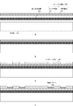
- FIG. 1 It is a figure which shows an example of the top view of the semiconductor laser drive device 10 in embodiment of this technique. It is a figure which shows an example of the cross-sectional view of the semiconductor laser driving apparatus 10 in the 1st Embodiment of this technique. It is a figure which shows the definition of the overlap amount of the laser driver 200 and the semiconductor laser 300 in embodiment of this technique. It is a figure which shows the numerical example of the wiring inductance with respect to a wiring length L and a wiring width W when a wiring pattern is formed by an additive method. It is a figure which shows the numerical example of the wiring inductance with respect to the wiring length L and the wiring width W when the wiring pattern is formed by the subtractive method.
- FIG. 1 shows an example of the top view of the semiconductor laser drive device 10 in embodiment of this technique. It is a figure which shows an example of the cross-sectional view of the semiconductor laser driving apparatus 10 in the 1st Embodiment of this technique. It is a figure which shows the definition of the overlap amount of the laser driver
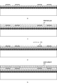
- FIG. 1 is a first diagram showing an example of a step of processing a copper land and a copper wiring layer (RDL) in the manufacturing process of the laser driver 200 according to the embodiment of the present technology.
- FIG. 2 is a second diagram showing an example of a step of processing a copper land and a copper wiring layer (RDL) in the manufacturing process of the laser driver 200 according to the embodiment of the present technology.
- It is the first figure which shows an example of the manufacturing process of the substrate 100 in embodiment of this technique.
- It is a 2nd figure which shows an example of the manufacturing process of the substrate 100 in embodiment of this technique.
- FIG. 3 is a third diagram showing an example of a manufacturing process of the substrate 100 according to the embodiment of the present technology.
- FIG. 4 is a fourth diagram showing an example of a manufacturing process of the substrate 100 according to the embodiment of the present technology.
- FIG. 5 is a fifth diagram showing an example of a manufacturing process of the substrate 100 according to the embodiment of the present technology. It is a figure which shows an example of the manufacturing process of the semiconductor laser driving apparatus 10 in the 1st Embodiment of this technique. It is a figure which shows an example of the sectional view of the semiconductor laser driving apparatus 10 in the 2nd Embodiment of this technique. It is a figure which shows an example of the manufacturing process of the semiconductor laser driving apparatus 10 in the 2nd Embodiment of this technique. It is a figure which shows an example of the manufacturing process of the semiconductor laser driving apparatus 10 in the 2nd Embodiment of this technique.
- FIG. 1 is a diagram showing an example of a top view of the semiconductor laser drive device 10 according to the embodiment of the present technology.
- the semiconductor laser drive device 10 is intended for distance measurement by ToF. Although the ToF is not as good as a structured light, it has high depth accuracy and can operate without problems even in a dark environment. In addition, in terms of simplicity of device configuration and cost, it is considered that there are many merits compared to other methods such as structured lights and stereo cameras.
- the semiconductor laser 300, the photodiode 400, and the passive component 500 are electrically connected and mounted on the surface of the substrate 100 in which the laser driver 200 is built.
- the substrate 100 As the substrate 100, a printed wiring board is assumed.
- the semiconductor laser 300 is a semiconductor device that emits laser light by passing an electric current through the PN junction of a compound semiconductor.
- a vertical cavity surface emitting laser (VCSEL: Vertical Cavity Surface Emitting Laser) is assumed.
- VCSEL Vertical Cavity Surface Emitting Laser
- it may be either a back-emitting type or a front-emitting type.
- the compound semiconductor used for example, aluminum gallium arsenide (AlGaAs), indium gallium arsenide phosphorus (InGaAsP), aluminum gallium indium phosphorus (AlGaInP), gallium nitride (GaN) and the like are assumed.
- the laser driver 200 is a driver integrated circuit (IC: Integrated Circuit) for driving the semiconductor laser 300.
- the laser driver 200 is built in the substrate 100 in a face-up state.
- IC Integrated Circuit
- the photodiode 400 is a diode for detecting light.
- the photodiode 400 is used for APC control (Automatic Power Control) for monitoring the light intensity of the semiconductor laser 300 and maintaining the output of the semiconductor laser 300 constant.
- APC control Automatic Power Control
- the passive component 500 is a circuit component other than an active element such as a capacitor and a resistor.
- the passive component 500 includes a decoupling capacitor for driving the semiconductor laser 300.
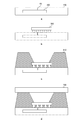
- FIG. 2 is a diagram showing an example of a cross-sectional view of the semiconductor laser driving device 10 according to the first embodiment of the present technology.
- the substrate 100 has a built-in laser driver 200, and a semiconductor laser 300 or the like is mounted on the surface thereof.
- the connection between the semiconductor laser 300 and the laser driver 200 on the substrate 100 is made via the connection via 101.
- This connection via 101 it is possible to shorten the wiring length.
- the connection via 101 is an example of the connection wiring described in the claims.
- the semiconductor laser 300 is flip-chip mounted on the substrate 100. Therefore, a solder bump 301 is formed at the connection terminal portion of the semiconductor laser 300.
- solder bump 301 is formed at the connection terminal portion of the semiconductor laser 300.
- other materials such as copper (Cu) pillar bumps and gold (Au) bumps may be used as the connection terminal portion.
- MUF Mold UnderFill
- the semiconductor laser 300, the photodiode 400 and the passive component 500 mounted on the surface of the substrate 100 are surrounded by the MUF610. Therefore, the MUF610 forms an underfill of the connection terminal portion of the semiconductor laser 300, and at the same time, a side wall portion is formed at the same time.
- a thermosetting resin is assumed as the material of this MUF610.
- the upper surface surrounded by the MUF 610 is covered with the diffuser plate 700.
- the diffuser plate 700 is an optical element for diffusing the laser beam from the semiconductor laser 300, and is also called a diffuser.
- FIG. 3 is a diagram showing a definition of an overlap amount between the laser driver 200 and the semiconductor laser 300 in the embodiment of the present technology.
- the two are arranged so as to overlap each other when viewed from the upper surface.
- half of the region of the semiconductor laser 300 is overlapped with the laser driver 200 when viewed from the upper surface.
- the amount of overlap in this case is defined as 50%.
- the overlap amount is larger than 0% in order to provide the area for the connection via 101 described above.
- the overlap amount is preferably 50% or less. Therefore, by setting the overlap amount to be larger than 0% and 50% or less, it is possible to reduce the wiring inductance and obtain good heat dissipation characteristics.
- the inductance IDC [ ⁇ H] of a straight lead wire having a circular cross section having a length L [mm] and a radius R [mm] is expressed by the following equation in free space.
- ln represents the natural logarithm.
- IDC 0.0002L ⁇ (ln (2L / R) -0.75)
- the inductance IDC [ ⁇ H] of the strip line (board wiring pattern) having a length L [mm], a width W [mm], and a thickness H [mm] is expressed by the following equation in free space.
- IDC 0.0002L ⁇ (ln (2L / (W + H))) +0.2235 ((W + H) / L) +0.5)
- FIGS. 4 and 5 are trial calculations of the wiring inductance [nH] between the laser driver built inside the printed wiring board and the semiconductor laser electrically connected to the upper part of the printed wiring board.
- FIG. 4 is a diagram showing a numerical example of the wiring inductance with respect to the wiring length L and the wiring width W when the wiring pattern is formed by the additive method.
- the additive method is a method of forming a pattern by depositing copper only on a necessary portion of the insulating resin surface.
- FIG. 5 is a diagram showing a numerical example of the wiring inductance with respect to the wiring length L and the wiring width W when the wiring pattern is formed by the subtractive method.
- Subtractive is a method of forming a pattern by etching an unnecessary part of a copper-clad laminate.
- the wiring inductance is preferably 0.5 nH or less, and more preferably 0.3 nH or less, assuming that it is driven at several hundreds of megahertz. Therefore, in consideration of the above estimation results, the wiring length between the semiconductor laser 300 and the laser driver 200 is preferably 0.5 mm or less, and more preferably 0.3 mm or less. Conceivable.
- [Production method] 6 and 7 are diagrams showing an example of a step of processing a copper land and a copper wiring layer (RDL) in the manufacturing process of the laser driver 200 according to the embodiment of the present technology.
- RDL copper wiring layer
- an I / O pad 210 made of, for example, aluminum is formed on the semiconductor wafer. Then, a protective insulating layer 220 such as SiN is formed on the surface, and the region of the I / O pad 210 is opened.
- a surface protective film 230 made of polyimide (PI: Polyimide) or polybenzoxazole (PBO: Polybenzoxazole) is formed, and the region of the I / O pad 210 is opened.
- titanium tungsten (TiW) of about several tens to 100 nm and copper (Cu) of about 100 to 1,000 nm are continuously sputtered to form an adhesion layer and a seed layer 240.
- refractory metals such as chromium (Cr), nickel (Ni), titanium (Ti), titanium copper (TiCu), and platinum (Pt) and their alloys are applied to the adhesion layer. You may. Further, in addition to copper (Cu), nickel (Ni), silver (Ag), gold (Au), or an alloy thereof may be applied to the seed layer.
- the photoresist 250 is patterned in order to form a copper land and a copper wiring layer for electrical bonding. Specifically, it is formed by each step of surface cleaning, resist coating, drying, exposure, and development.
- a copper land and a copper wiring layer (RDL) 260 for electrical bonding are formed on the adhesion layer and the seed layer 240 by a plating method.
- the plating method for example, an electrolytic copper plating method, an electrolytic nickel plating method, or the like can be used.
- the diameter of the copper land is about 50 to 100 micrometers
- the thickness of the copper wiring layer is about 3 to 10 micrometers
- the minimum width of the copper wiring layer is about 10 micrometers.
- the photoresist 250 is removed, the copper land of the semiconductor chip and the copper wiring layer (RDL) 260 are masked, and dry etching is performed.
- dry etching for example, ion milling that irradiates an argon ion beam can be used.
- the adhesion layer and the seed layer 240 in the unnecessary region can be selectively removed, and the copper land and the copper wiring layer are separated from each other.
- FIGS. 8 to 12 are diagrams showing an example of a manufacturing process of the substrate 100 according to the embodiment of the present technology.
- a peelable copper foil 130 having a two-layer structure of an ultrathin copper foil 132 and a carrier copper foil 131 is roll-laminated or laminated on a support plate 110 via an adhesive resin layer 120. Thermocompression bonding is performed on one side by pressing.
- a substrate made of an inorganic material, a metal material, a resin material, or the like can be used as the support plate 110.
- silicon (Si) glass, ceramic, copper, copper-based alloy, aluminum, aluminum alloy, stainless steel, polyimide resin, and epoxy resin can be used.
- a carrier copper foil 131 having a thickness of 18 to 35 micrometers is vacuum-adhered to an ultrathin copper foil 132 having a thickness of 2 to 5 micrometers.
- the peelable copper foil 130 for example, 3FD-P3 / 35 (manufactured by Furukawa Circuit Foil Co., Ltd.), MT-18S5DH (manufactured by Mitsui Mining & Smelting Co., Ltd.) and the like can be used.
- the resin material of the adhesive resin layer 120 includes epoxy resin, polyimide resin, PPE resin, phenol resin, PTFE resin, silicon resin, polybutadiene resin, polyester resin, melamine resin, urea resin, and PPS containing a reinforcing material for glass fibers.
- Organic resins such as resins and PPO resins can be used.
- the reinforcing material in addition to glass fiber, aramid non-woven fabric, aramid fiber, polyester fiber and the like can also be used.
- a plating base conductive layer (not shown) having a thickness of 0.5 to 3 micrometers is applied to the surface of the ultrathin copper foil 132 of the peelable copper foil 130 by electroless copper plating.
- a conductive layer under the electrolytic copper plating that forms a wiring pattern is formed next.
- this electroless copper plating treatment is omitted, the electrode for electrolytic copper plating is directly brought into contact with the peelable copper foil 130, and the electrolytic copper plating treatment is directly applied on the peelable copper foil 130.
- a wiring pattern may be formed.
- a photosensitive resist is attached to the surface of the support plate by roll laminating to form a resist pattern (solder resist 140) for a wiring pattern.
- a photosensitive resist for example, a dry film plating resist can be used.
- a wiring pattern 150 having a thickness of about 15 micrometers is formed by electrolytic copper plating.
- the plating resist is peeled off.
- the surface of the wiring pattern is roughened to improve the adhesiveness between the interlayer insulating resin and the wiring pattern.
- the roughening treatment can be performed by a blackening treatment by a redox treatment or a soft etching treatment of a hydrogen peroxide system.
- the interlayer insulating resin 161 is thermocompression bonded on the wiring pattern by roll laminating or laminating press.
- an epoxy resin having a thickness of 45 micrometers is roll-laminated.
- glass epoxy resin copper foils of arbitrary thickness are laminated and thermocompression bonded with a laminated press.
- the resin material of the interlayer insulating resin 161 include organic resins such as epoxy resin, polyimide resin, PPE resin, phenol resin, PTFE resin, silicon resin, polybutadiene resin, polyester resin, melamine resin, urea resin, PPS resin, and PPO resin. Can be used.
- these resins alone can be used, or a combination of resins obtained by mixing a plurality of resins or preparing a compound can also be used. Further, an interlayer insulating resin in which an inorganic filler is contained in these materials or a reinforcing material of glass fiber is mixed can also be used.
- via holes for interlayer electrical connection are formed by a laser method or a photoetching method.
- the interlayer insulating resin 161 is a thermosetting resin
- via holes are formed by a laser method.
- the laser beam an ultraviolet laser such as a harmonic YAG laser or an excimer laser, or an infrared laser such as a carbon dioxide gas laser can be used.
- a via hole is formed by laser light, a thin resin film may remain on the bottom of the via hole, so a desmear treatment is performed.
- the resin is swollen with a strong alkali, and the resin is decomposed and removed using an oxidizing agent such as chromic acid or an aqueous solution of permanganate. It can also be removed by plasma treatment or sandblasting with an abrasive.
- an oxidizing agent such as chromic acid or an aqueous solution of permanganate. It can also be removed by plasma treatment or sandblasting with an abrasive.
- the interlayer insulating resin 161 is a photosensitive resin
- via holes 170 are formed by a photoetching method. That is, the via hole 170 is formed by developing after exposing with ultraviolet rays through a mask.
- a photosensitive resist is attached by roll laminating to the surface of the interlayer insulating resin 161 whose surface is electroless plated.
- a dry film photosensitive plated resist film can be used as the photosensitive resist in this case.
- a plating resist pattern in which the via hole 170 portion and the wiring pattern portion are opened is formed.
- the opening portion of the plating resist pattern is subjected to electrolytic copper plating treatment with a thickness of 15 micrometers.
- the plating resist is peeled off, and the electroless plating remaining on the interlayer insulating resin is removed by flash etching of a hydrogen peroxide system, so that the via holes are filled with copper plating as shown in h in FIG. Form a wiring pattern with 170. Then, the same roughening step of the wiring pattern and the forming step of the interlayer insulating resin 162 are repeated.
- DAF Die Attach Film
- the interlayer insulating resin 163 is thermocompression bonded by roll laminating or a laminated press.
- the same via hole processing, desmear treatment, roughening treatment, electroless plating treatment, and electrolytic plating treatment as before are performed.
- the processing of the shallow via hole 171 on the copper land of the laser driver 200, the processing of the deep via hole 172 one layer below, the desmear treatment, and the roughening treatment are performed at the same time.
- the shallow via hole 171 is a filled via filled with copper plating.
- the size and depth of vias are on the order of 20 to 30 micrometers, respectively.
- the size of the land is about 60 to 80 micrometers in diameter.
- the deep via hole 172 is a so-called conformal via in which copper plating is applied only to the outside of the via.
- the size and depth of the vias are on the order of 80 to 150 micrometers, respectively.
- the size of the land is about 150 to 200 micrometers in diameter. It is desirable that the deep via hole 172 is arranged via an insulating resin of about 100 micrometers from the outer shape of the laser driver 200.
- the same interlayer insulating resin as before is thermocompression bonded by roll laminating or laminating press. At this time, the inside of the conformal via is filled with the interlayer insulating resin. Next, the same via hole processing, desmear treatment, roughening treatment, electroless plating treatment, and electrolytic plating treatment as before are performed.
- the support plate 110 is separated by peeling from the interface between the carrier copper foil 131 of the peelable copper foil 130 and the ultrathin copper foil 132.
- the ultrathin copper foil 132 and the conductive layer underneath the plating are removed by using sulfuric acid-hydrogen peroxide soft etching to obtain a component-embedded substrate with an exposed wiring pattern. Can be done.
- a solder resist 180 having a pattern having an opening in the land portion of the wiring pattern is printed on the exposed wiring pattern.
- the solder resist 180 can also be formed by a roll coater using a film type.
- electroless Ni plating of 3 micrometers or more is formed on the land portion of the opening of the solder resist 180, and electroless Au plating of 0.03 micrometers or more is formed on the electroless Ni plating.
- Electroless Au plating may be formed over 1 micrometer. Furthermore, it is also possible to precoat solder on it.
- electrolytic Ni plating may be formed at 3 micrometers or more in the opening of the solder resist 180, and electrolytic Au plating may be formed at 0.5 micrometers or more on the electrolytic Ni plating.
- an organic rust preventive film may be formed in the opening of the solder resist 180 in addition to metal plating.
- cream solder may be printed and applied to the land for external connection as a connection terminal, and a solder ball BGA (Ball Grid Array) may be mounted.
- a connection terminal a copper core ball, a copper pillar bump, a land grid array (LGA: Land Grid Array), or the like may be used.
- the semiconductor laser 300, the photodiode 400 and the passive component 500 are mounted on the surface of the substrate 100 manufactured in this manner, and the MUF 610 and the diffuser plate 700 are attached.
- the outer shape is processed with a dicer or the like to separate the pieces into individual pieces after performing the process in the form of a collective substrate.
- peelable copper foil 130 and the support plate 110 are used has been described in the above-mentioned steps, it is also possible to use a copper-clad laminate (CCL: Copper Clad Laminate) instead of these. Further, as a manufacturing method for incorporating the component into the substrate, a method of forming a cavity in the substrate and mounting the component may be used.
- CCL Copper Clad Laminate
- FIG. 13 is a diagram showing an example of a manufacturing process of the semiconductor laser driving device 10 according to the first embodiment of the present technology.
- the semiconductor laser 300 is mounted on the substrate 100 by mass reflow (mass reflow) or thermocompression bonding (Thermal Compression Bonding).
- the periphery of the connection terminal portion of the semiconductor laser 300 and the portion corresponding to the side wall of the semiconductor laser drive device are integrally molded by the MUF610.
- the molding method may be either a transfer molding method or a compression molding method.
- the emitted light surface of the semiconductor laser 300 needs to have a structure that is not covered by the MUF610. Therefore, by using a mold, the MUF610 is molded so as not to be filled.
- the diffuser plate 700 is attached.
- the outer wall of the semiconductor laser driving device 10 can be formed at the same time while protecting the connection terminal portion of the semiconductor laser 300 by using the MUF 610.
- the wiring inductance can be reduced by making the electrical connection between the semiconductor laser 300 and the laser driver 200 via the connection via 101. .. Specifically, by setting the wiring length between the two to 0.5 mm or less, the wiring inductance thereof can be set to 0.5 nanohenry or less. Further, by reducing the amount of overlap between the semiconductor laser 300 and the laser driver 200 to 50% or less, a certain number of thermal vias can be arranged directly under the semiconductor laser 300, and good heat dissipation characteristics can be obtained. be able to. Further, by using the MUF 610, the outer wall of the semiconductor laser driving device 10 can be formed at the same time while protecting the connection terminal portion of the semiconductor laser 300.
- Second Embodiment> In the above-described first embodiment, an example in which the solder bump 301 is formed on the connection terminal portion of the semiconductor laser 300 has been described, but the structure of the connection terminal portion is not limited to this. In this second embodiment, an example in which the semiconductor laser 300 and the substrate 100 are connected by bonding wires will be described. Since the substrate 100 itself containing the laser driver 200 is the same as that of the first embodiment described above, detailed description thereof will be omitted.
- FIG. 14 is a diagram showing an example of a cross-sectional view of the semiconductor laser driving device 10 according to the second embodiment of the present technology.
- a bonding wire 302 is formed as a connection terminal portion of the semiconductor laser 300. As a result, the semiconductor laser 300 and the wiring of the substrate 100 are electrically connected.
- the semiconductor laser 300, the photodiode 400, and the passive component 500 mounted on the surface of the substrate 100 are surrounded by the mold resin 620.
- the mold resin 620 is an example of the sealing portion described in the claims.
- the upper surface surrounded by the mold resin 620 is covered with the diffuser plate 700.
- FIG. 15 is a diagram showing an example of a manufacturing process of the semiconductor laser driving device 10 according to the second embodiment of the present technology.
- the semiconductor laser 300 is die-attached to the substrate 100 with a conductive paste, and the bonding wire 302 is formed. As a result, the semiconductor laser 300 and the wiring of the substrate 100 are electrically connected.
- the periphery of the semiconductor laser 300 and the portion corresponding to the side wall of the semiconductor laser driving device 10 are integrally molded with a thermosetting resin.
- the molding method may be either a transfer molding method or a compression molding method.
- the diffuser plate 700 is attached.
- the outer wall of the semiconductor laser driving device 10 can be formed at the same time while protecting the bonding wire 302 by using the mold resin 620.
- the outer wall of the semiconductor laser driving device 10 is protected while the bonding wire 302 is protected by using the mold resin 620. Can be formed at the same time.
- the MUF610 is used to form the outer wall of the semiconductor laser drive device 10 and the connection terminal portion of the semiconductor laser 300 is protected at the same time, but both may be formed individually. It is possible.
- this third embodiment an example in which the capillary underfill is used will be described. Since the substrate 100 itself containing the laser driver 200 is the same as that of the first embodiment described above, detailed description thereof will be omitted.
- FIG. 16 is a diagram showing an example of a cross-sectional view of the semiconductor laser driving device 10 according to the third embodiment of the present technology.
- Solder bumps 301 are formed on the connection terminals of the semiconductor laser 300 in the same manner as in the first embodiment described above. Similarly, other materials such as copper (Cu) pillar bumps and gold (Au) bumps may be used as the connection terminal portion.
- Cu copper
- Au gold
- connection terminal portion of the semiconductor laser 300 is surrounded by a CUF (Capillary UnderFill) 630.
- a CUF Chemical UnderFill
- a thermosetting resin is assumed.
- CUF630 is an example of the sealing portion described in the claims.
- a side wall 600 is formed around the semiconductor laser 300 mounted on the surface of the substrate 100.
- the upper surface surrounded by the side wall 600 is covered with the diffuser plate 700.
- FIG. 17 is a diagram showing an example of a manufacturing process of the semiconductor laser driving device 10 according to the third embodiment of the present technology.
- the semiconductor laser 300 is mounted on the substrate 100 by mass reflow or thermocompression bonding.
- CUF630 is applied.
- the underfill resin advances to the depth of the gap between the semiconductor laser 300 and the substrate 100 by utilizing the capillary phenomenon, and seals the joint surface between the semiconductor laser 300 and the substrate 100 with the resin.
- the underfill resin of CUF630 is hardened by thermosetting, a step of curing the underfill resin is provided.
- the periphery of the semiconductor laser 300 and the portion corresponding to the side wall 600 of the semiconductor laser driving device 10 are integrally molded with a thermosetting resin.
- the molding method may be either a transfer molding method or a compression molding method.
- a side wall formed separately in advance may be attached. After that, the diffuser plate 700 is mounted on the side wall 600.
- the outer wall of the semiconductor laser driving device 10 can be formed by the side wall 600, apart from the structure in which the CUF 630 is used to protect the connection terminal portion of the semiconductor laser 300.
- the connection terminal portion of the semiconductor laser 300 can be protected by the CUF 630.
- FIG. 18 is a diagram showing a system configuration example of the electronic device 800, which is an application example of the embodiment of the present technology.
- the electronic device 800 is a mobile terminal equipped with the semiconductor laser drive device 10 according to the above-described embodiment.
- the electronic device 800 includes an imaging unit 810, a semiconductor laser driving device 820, a shutter button 830, a power button 840, a control unit 850, a storage unit 860, a wireless communication unit 870, a display unit 880, and a battery. It is equipped with 890.
- the image pickup unit 810 is an image sensor that captures a subject.
- the semiconductor laser driving device 820 is the semiconductor laser driving device 10 according to the above-described embodiment.
- the shutter button 830 is a button for instructing the imaging timing in the imaging unit 810 from the outside of the electronic device 800.
- the power button 840 is a button for instructing the on / off of the power of the electronic device 800 from the outside of the electronic device 800.
- the control unit 850 is a processing unit that controls the entire electronic device 800.
- the storage unit 860 is a memory that stores data and programs necessary for the operation of the electronic device 800.
- the wireless communication unit 870 performs wireless communication with the outside of the electronic device 800.
- the display unit 880 is a display for displaying an image or the like.
- the battery 890 is a power supply source that supplies power to each part of the electronic device 800.
- a specific phase (for example, rise timing) of the light emission control signal that controls the image pickup unit 810 and the semiconductor laser drive device 820 is set to 0 degrees, and the amount of light received from 0 degrees to 180 degrees is detected as Q1 to detect 180 degrees to 360 degrees. The amount of received light up to is detected as Q2. Further, the imaging unit 810 detects the light receiving amount from 90 degrees to 270 degrees as Q3, and detects the light receiving amount from 270 degrees to 90 degrees as Q4.
- the unit of the distance d is, for example, meters (m).
- c is the speed of light, the unit of which is, for example, meters per second (m / s).
- arctan is the inverse function of the tangent function.
- the value of "(Q3-Q4) / (Q1-Q2)" indicates the phase difference between the irradiation light and the reflected light.
- ⁇ indicates the pi.
- f is the frequency of the irradiation light, and the unit thereof is, for example, megahertz (MHz).
- FIG. 19 is a diagram showing an example of an external configuration of an electronic device 800, which is an application example of the embodiment of the present technology.
- This electronic device 800 is housed in a housing 801, has a power button 840 on the side surface, and has a display unit 880 and a shutter button 830 on the front surface. Further, an optical region of the imaging unit 810 and the semiconductor laser driving device 820 is provided on the back surface.
- the normal captured image 881 can be displayed on the display unit 880, but also the depth image 882 according to the distance measurement result using ToF can be displayed.
- a mobile terminal such as a smartphone is illustrated as the electronic device 800, but the electronic device 800 is not limited to this, and may be, for example, a digital camera, a game machine, a wearable device, or the like. Good.
- the present technology can have the following configurations.
- Bumps are formed on the connection terminals of the semiconductor laser.
- the semiconductor laser driving device according to (2) above, wherein the sealing portion is a mold underfill that covers a region including the bump.
- a bonding wire is formed at the connection terminal portion of the semiconductor laser.
- the semiconductor laser driving device is a mold resin that covers a region including the bonding wire.
- the semiconductor laser driving device further comprising a diffuser plate that covers the upper part of the region surrounded by the outer wall.
- the semiconductor laser driving device according to any one of (1) to (5) above, wherein the emitted light surface of the semiconductor laser has a structure that is not covered by the sealing portion.
- the semiconductor laser driving device is a capillary underfill.
- connection wiring is via a connection via provided on the substrate.
- connection wiring is via a connection via provided on the substrate.
- connection wiring is via a connection via provided on the substrate.
- connection wiring is via a connection via provided on the substrate.
- connection wiring is via a connection via provided on the substrate.
- (11) The semiconductor laser driving device according to (10), wherein a portion of 50% or less of the area of the semiconductor laser is arranged above the laser driver.
- An electronic device including a sealing portion for sealing a connection terminal portion of the semiconductor laser with respect to the substrate.
- a method for manufacturing a semiconductor laser driving device comprising a procedure for forming a sealing portion for sealing the connection terminal portion of the semiconductor laser with respect to the substrate.
Abstract
半導体レーザ駆動装置において、半導体レーザとレーザドライバとの間の配線インダクタンスを低減する。 半導体レーザ駆動装置は、基板と、レーザドライバと、半導体レーザとを備える。基板は、レーザドライバを内蔵する。半導体レーザは、半導体レーザ駆動装置の基板の一方の面に実装される。接続配線は、レーザドライバと半導体レーザとを0.5ナノヘンリー以下の配線インダクタンスにより電気接続する。封止部は、基板に対する半導体レーザの接続端子部を封止する。
Description
本技術は、半導体レーザ駆動装置に関する。詳しくは、レーザドライバ内蔵基板と半導体レーザとを備える半導体レーザ駆動装置、電子機器、および、半導体レーザ駆動装置の製造方法に関する。
従来、測距機能を持つ電子装置において、ToF(Time of Flight)と呼ばれる測距方式がよく用いられている。このToFは、発光部がサイン波や矩形波の照射光を物体に照射し、その物体からの反射光を受光部が受光して、測距演算部が照射光と反射光との位相差から距離を測定する方式である。そのような測距機能を実現するため、発光素子と、その発光素子を駆動する電子半導体チップとをケース内に収容して一体化した光モジュールが知られている。例えば、基板の電極パターン上に整列して実装されたレーザーダイオードアレイと、レーザーダイオードアレイに電気的に接続されたドライバICとを備える光モジュールが提案されている(例えば、特許文献1参照。)。
上述の従来技術では、レーザーダイオードアレイとドライバICとを光モジュールとして一体化して構成している。しかしながら、この従来技術では、レーザーダイオードアレイとドライバICとを複数のワイヤによって電気的に接続しており、その間の配線インダクタンスが大きくなり、半導体レーザの駆動波形が歪んでしまうおそれがある。これは、数百メガヘルツで駆動させるToFでは特に問題となる。
本技術はこのような状況に鑑みて生み出されたものであり、半導体レーザ駆動装置において、半導体レーザとレーザドライバとの間の配線インダクタンスを低減することを目的とする。
本技術は、上述の問題点を解消するためになされたものであり、その第1の側面は、レーザドライバを内蔵する基板と、上記基板の一方の面に実装された半導体レーザと、上記レーザドライバと上記半導体レーザとを0.5ナノヘンリー以下の配線インダクタンスにより電気接続する接続配線と、上記基板に対する上記半導体レーザの接続端子部を封止する封止部とを具備する半導体レーザ駆動装置およびその半導体レーザ駆動装置を備える電子機器である。これにより、レーザドライバと半導体レーザとを0.5ナノヘンリー以下の配線インダクタンスにより電気接続するという作用をもたらす。
また、この第1の側面において、上記封止部は、上記半導体レーザを含む領域を囲う外壁を形成するようにしてもよい。これにより、半導体レーザの接続端子部の封止構造と外壁とを同時に形成するという作用をもたらす。
また、この第1の側面において、上記半導体レーザの上記接続端子部にはバンプが形成され、上記封止部は、上記バンプを含む領域を覆うモールドアンダーフィルであってもよい。これにより、モールドアンダーフィルによって外壁を同時に形成するという作用をもたらす。
また、この第1の側面において、上記半導体レーザの上記接続端子部にはボンディングワイヤが形成され、上記封止部は、上記ボンディングワイヤを含む領域を覆うモールド樹脂であってもよい。これにより、ボンディングワイヤを含む領域を覆うモールド樹脂によって外壁を同時に形成するという作用をもたらす。
また、この第1の側面において、上記外壁に囲まれた領域の上方を覆う拡散板をさらに具備してもよい。これにより、封止部によって形成された外壁に拡散板を取り付けるという作用をもたらす。
また、この第1の側面において、上記半導体レーザの出射光面は、上記封止部によって覆われない構造であってもよい。これにより、半導体レーザから出射される光を妨げることなく、半導体レーザの接続端子部を封止するという作用をもたらす。
また、この第1の側面において、上記封止部は、キャピラリーアンダーフィルであってもよい。これにより、外壁とは別に半導体レーザの接続端子部を封止するという作用をもたらす。
また、この第1の側面において、上記接続配線は、0.5ミリメートル以下の長さを備えることが望ましい。また、上記接続配線は、0.3ミリメートル以下であることがより好ましい。
また、この第1の側面において、上記接続配線は、上記基板に設けられる接続ビアを介してもよい。これにより、配線長を短くするという作用をもたらす。
また、この第1の側面において、上記半導体レーザは、その一部が上記レーザドライバの上方に重ねて配置されるようにしてもよい。この場合において、上記半導体レーザは、その面積の50%以下の部分が上記レーザドライバの上方に重ねて配置されるようにしてもよい。
また、本技術の第2の側面は、支持板の上面にレーザドライバを形成する手順と、上記レーザドライバの接続配線を形成して上記レーザドライバを内蔵する基板を形成する手順と、上記基板の一方の面に半導体レーザを実装して上記接続配線を介して上記レーザドライバと上記半導体レーザとを0.5ナノヘンリー以下の配線インダクタンスにより電気接続する接続配線を形成する手順と、上記基板に対する上記半導体レーザの接続端子部を封止する封止部を形成する手順とを具備する半導体レーザ駆動装置の製造方法である。これにより、レーザドライバと半導体レーザとを0.5ナノヘンリー以下の配線インダクタンスにより電気接続する半導体レーザ駆動装置を製造するという作用をもたらす。
以下、本技術を実施するための形態(以下、実施の形態と称する)について説明する。説明は以下の順序により行う。
1.第1の実施の形態(モールドアンダーフィルによるバンプ保護の例)
2.第2の実施の形態(モールド樹脂によるボンディングワイヤ保護の例)
3.第3の実施の形態(キャピラリーアンダーフィルによるバンプ保護の例)
4.適用例
1.第1の実施の形態(モールドアンダーフィルによるバンプ保護の例)
2.第2の実施の形態(モールド樹脂によるボンディングワイヤ保護の例)
3.第3の実施の形態(キャピラリーアンダーフィルによるバンプ保護の例)
4.適用例
<1.第1の実施の形態>
[半導体レーザ駆動装置]
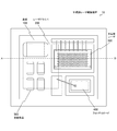
図1は、本技術の実施の形態における半導体レーザ駆動装置10の上面図の一例を示す図である。
[半導体レーザ駆動装置]
図1は、本技術の実施の形態における半導体レーザ駆動装置10の上面図の一例を示す図である。
この半導体レーザ駆動装置10は、ToFによる距離の測定を想定したものである。ToFは、ストラクチャードライトほどではないものの奥行き精度が高く、また、暗い環境下でも問題なく動作可能という特徴を有する。他にも、装置構成の単純さや、コストなどにおいて、ストラクチャードライトやステレオカメラなどの他の方式と比べてメリットが多いと考えられる。
この半導体レーザ駆動装置10では、レーザドライバ200を内蔵する基板100の表面に、半導体レーザ300、フォトダイオード400および受動部品500がワイヤボンディングにより電気接続されて実装される。基板100としては、プリント配線板が想定される。
半導体レーザ300は、化合物半導体のPN接合に電流を流すことにより、レーザ光を放射する半導体デバイスである。具体的には、垂直共振器面発光レーザ(VCSEL:Vertical Cavity Surface Emitting Laser)が想定される。ただし、裏面発光型、または、表面発光型の何れであってもよい。ここで、利用される化合物半導体としては、例えば、アルミニウムガリウム砒素(AlGaAs)、インジウムガリウム砒素リン(InGaAsP)、アルミニウムガリウムインジウムリン(AlGaInP)、ガリウムナイトライド(GaN)などが想定される。
レーザドライバ200は、半導体レーザ300を駆動するためのドライバ集積回路(IC:Integrated Circuit)である。このレーザドライバ200は、フェイスアップ状態で基板100に内蔵される。半導体レーザ300との間の電気接続については、配線インダクタンスを低減させる必要があるため、出来る限り短い配線長とすることが望ましい。この具体的数値については後述する。
フォトダイオード400は、光を検出するためのダイオードである。このフォトダイオード400は、半導体レーザ300の光強度を監視して、半導体レーザ300の出力を一定に維持するためのAPC制御(Automatic Power Control)に用いられる。
受動部品500は、コンデンサおよび抵抗などの能動素子以外の回路部品である。この受動部品500には、半導体レーザ300を駆動するためのデカップリングコンデンサが含まれる。
図2は、本技術の第1の実施の形態における半導体レーザ駆動装置10の断面図の一例を示す図である。
上述のように、基板100はレーザドライバ200を内蔵し、その表面には半導体レーザ300などが実装される。基板100における半導体レーザ300とレーザドライバ200との間の接続は、接続ビア101を介して行われる。この接続ビア101を用いることにより、配線長を短くすることが可能となる。なお、接続ビア101は、特許請求の範囲に記載の接続配線の一例である。
半導体レーザ300は、基板100にフリップチップ実装される。そのため、半導体レーザ300の接続端子部には、半田バンプ301が形成される。ただし、この接続端子部としては、銅(Cu)ピラーバンプ、金(Au)バンプなどの他の材料を用いてもよい。
半導体レーザ300の接続端子部においては、接続信頼性を担保するためにアンダーフィルで埋める必要がある。この第1の実施の形態においては、MUF(Mold UnderFill:モールドアンダーフィル)610が用いられる。このMUF610は、特許請求の範囲に記載の封止部の一例である。
また、基板100の表面に実装された半導体レーザ300、フォトダイオード400および受動部品500は、MUF610によって囲まれる。したがって、MUF610によって半導体レーザ300の接続端子部のアンダーフィルが形成されるとともに、側壁部分が同時に形成されることになる。このMUF610の材料としては、例えば、熱硬化性樹脂が想定される。
MUF610によって囲まれた上面は、拡散板700によって覆われる。この拡散板700は、半導体レーザ300からのレーザ光を拡散させるための光学素子であり、ディフューザとも呼ばれる。
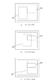
図3は、本技術の実施の形態におけるレーザドライバ200と半導体レーザ300とのオーバラップ量の定義を示す図である。
上述のように、半導体レーザ300とレーザドライバ200との間の接続は接続ビア101を介して行われることを想定しているため、上面から見ると両者は重なって配置されることになる。その一方で、半導体レーザ300の下面にはサーマルビアを設けることが望ましく、そのための領域を確保する必要もある。そこで、レーザドライバ200と半導体レーザ300の位置関係を明らかにするために、両者のオーバラップ量を以下のように定義する。
同図におけるaに示す配置では、上面から見て両者に重なる領域が存在しない。この場合のオーバラップ量を0%と定義する。一方、同図におけるcに示す配置では、上面から見て半導体レーザ300の全てがレーザドライバ200と重なっている。この場合のオーバラップ量を100%と定義する。
そして、同図におけるbに示す配置では、上面から見て半導体レーザ300の半分の領域がレーザドライバ200と重なっている。この場合のオーバラップ量を50%と定義する。
この実施の形態では、上述の接続ビア101のための領域を設けるために、オーバラップ量は0%よりも大きいことが望ましい。一方、半導体レーザ300の直下においてある程度の数のサーマルビア102を配置することを考慮すると、オーバラップ量は50%以下であることが望ましい。したがって、オーバラップ量を0%より大きく、50%以下とすることにより、配線インダクタンスを小さくするとともに、良好な放熱特性を得ることが可能となる。
[配線インダクタンス]
上述のように、半導体レーザ300とレーザドライバ200との間の接続においては、配線インダクタンスが問題となる。全ての導体には誘導成分があり、ToFシステムのような高周波領域では、極めて短いリード線のインダクタンスでも悪影響をおよぼすおそれがある。すなわち、高周波動作した際に、配線インダクタンスの影響によりレーザドライバ200から半導体レーザ300を駆動するための駆動波形が歪んでしまい、動作が不安定になるおそれがある。
上述のように、半導体レーザ300とレーザドライバ200との間の接続においては、配線インダクタンスが問題となる。全ての導体には誘導成分があり、ToFシステムのような高周波領域では、極めて短いリード線のインダクタンスでも悪影響をおよぼすおそれがある。すなわち、高周波動作した際に、配線インダクタンスの影響によりレーザドライバ200から半導体レーザ300を駆動するための駆動波形が歪んでしまい、動作が不安定になるおそれがある。
ここで、配線インダクタンスを計算するための理論式について検討する。例えば、長さL[mm]、半径R[mm]の円形断面を持つ直線リード線のインダクタンスIDC[μH]は、自由空間において次式により表される。ただし、lnは自然対数を表す。
IDC=0.0002L・(ln(2L/R)-0.75)
IDC=0.0002L・(ln(2L/R)-0.75)
また、例えば、長さL[mm]、幅W[mm]、厚さH[mm]のストリップ・ライン(基板配線パターン)のインダクタンスIDC[μH]は、自由空間において次式により表される。
IDC=0.0002L・(ln(2L/(W+H))
+0.2235((W+H)/L)+0.5)
IDC=0.0002L・(ln(2L/(W+H))
+0.2235((W+H)/L)+0.5)
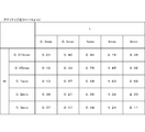
プリント配線板の内部に内蔵されたレーザドライバとプリント配線板の上部に電気接続された半導体レーザとの配線インダクタンス[nH]を試算したものが、図4および図5である。
図4は、アディティブ法により配線パターンを形成した場合の、配線長Lおよび配線幅Wに対する配線インダクタンスの数値例を示す図である。アディティブ法とは、絶縁樹脂面の必要な部分にだけ銅を析出させて、パターン形成する方法である。
図5は、サブトラクティブ法により配線パターンを形成した場合の、配線長Lおよび配線幅Wに対する配線インダクタンスの数値例を示す図である。サブトラクティブとは、銅張積層板の不要な部分をエッチングして、パターンを形成する方法である。
ToFシステムのような半導体レーザ駆動装置の場合、数百メガヘルツで駆動させることを想定すると、配線インダクタンスとしては0.5nH以下であることが望ましく、さらに0.3nH以下であることがより好ましい。したがって、上述の試算結果を考慮すると、半導体レーザ300とレーザドライバ200との間の配線長としては、0.5ミリメートル以下にすることが望ましく、さらに0.3ミリメートル以下であることがより好ましいと考えられる。
[製造方法]
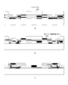
図6および図7は、本技術の実施の形態のレーザドライバ200の製造過程において銅ランドおよび銅配線層(RDL:Redistribution Layer)を加工する工程の一例を示す図である。
図6および図7は、本技術の実施の形態のレーザドライバ200の製造過程において銅ランドおよび銅配線層(RDL:Redistribution Layer)を加工する工程の一例を示す図である。
まず、図6におけるaに示すように、半導体ウェハにおいて、例えばアルミニウムなどによるI/Oパッド210が形成される。そして、表面にSiNなどの保護絶縁層220が成膜され、I/Oパッド210の領域が開孔される。
次に、図6におけるbに示すように、ポリイミド(PI:Polyimide)またはポリベンゾオキサゾール(PBO:Polybenzoxazole)による表面保護膜230が成膜され、I/Oパッド210の領域が開孔される。
次に、図6におけるcに示すように、数十乃至百nm程度のチタンタングステン(TiW)、百乃至千nm程度の銅(Cu)を連続スパッタして密着層およびシード層240を形成する。ここで、密着層は、チタンタングステン(TiW)の他にクロム(Cr)、ニッケル(Ni)、チタン(Ti)、チタン銅(TiCu)、プラチナ(Pt)等の高融点金属やその合金を適用してもよい。また、シード層には、銅(Cu)の他にニッケル(Ni)、銀(Ag)、金(Au)、または、その合金を適用してもよい。
次に、図7におけるdに示すように、電気接合用の銅ランドと銅配線層を形成するために、フォトレジスト250をパターニングする。具体的には、表面洗浄、レジスト塗布、乾燥、露光、現像の各工程によって形成する。
次に、図7におけるeに示すように、密着層およびシード層240の上にめっき法により、電気接合用の銅ランドおよび銅配線層(RDL)260を形成する。ここで、めっき法としては、例えば、電解銅めっき法や電解ニッケルめっき法などを用いることができる。また、銅ランドの直径は50乃至100マイクロメートル程度、銅配線層の厚さは3乃至10マイクロメートル程度、銅配線層の最小幅は10マイクロメートル程度が望ましい。
次に、図7におけるfに示すように、フォトレジスト250を除去し、半導体チップの銅ランドおよび銅配線層(RDL)260をマスクして、ドライエッチングを行う。ここで、ドライエッチングは、例えば、アルゴンイオンビームを照射するイオンミリングを用いることができる。このドライエッチングにより、不要領域の密着層およびシード層240を選択的に除去することができ、銅ランドおよび銅配線層が各々分離される。なお、この不要領域の除去は、王水、硝酸第二セリウムアンモニウムや水酸化カリウムの水溶液等のウエットエッチングでも可能だが、銅ランドおよび銅配線層を構成する金属層のサイドエッチや厚み減少を考慮するとドライエッチングの方が望ましい。
図8乃至図12は、本技術の実施の形態における基板100の製造工程の一例を示す図である。
まず、図8におけるaに示すように、支持板110に接着性樹脂層120を介して、極薄銅箔132とキャリア銅箔131の2層構造から成るピーラブル銅箔130を、ロールラミネートまたは積層プレスにより片面に熱圧着させる。
支持板110は、無機材料や金属材料、樹脂材料等からなる基板を使用することができる。例えば、シリコン(Si)、ガラス、セラミック、銅、銅系合金、アルミニウム、アルミ合金、ステンレス、ポリイミド樹脂、エポキシ樹脂を使用することができる。
ピーラブル銅箔130は、厚さ2乃至5マイクロメートルの極薄銅箔132に、厚さ18乃至35マイクロメートルのキャリア銅箔131を真空密着したものを用いる。ピーラブル銅箔130としては、例えば、3FD-P3/35(古河サーキットフォイル株式会社製)、MT-18S5DH(三井金属鉱業株式会社製)等を用いることができる。
接着性樹脂層120の樹脂材料としては、ガラス繊維の補強材入りの、エポキシ樹脂、ポリイミド樹脂、PPE樹脂、フェノール樹脂、PTFE樹脂、珪素樹脂、ポリブタジエン樹脂、ポリエステル樹脂、メラミン樹脂、ユリア樹脂、PPS樹脂、PPO樹脂などの有機樹脂を使用することができる。また、補強材としては、ガラス繊維以外に、アラミド不織布やアラミド繊維、ポリエステル繊維などを用いることもできる。
次に、図8におけるbに示すように、無電解銅めっき処理により、ピーラブル銅箔130の極薄銅箔132の表面に厚さ0.5乃至3マイクロメートルの(図示しない)めっき下地導電層を形成する。なお、この無電解銅めっき処理は、次に配線パターンを形成する電解銅めっきの下地の導電層を形成するものである。ただし、この無電解銅めっき処理を省略して、ピーラブル銅箔130に直接的に電解銅めっき用の電極を接触させて、ピーラブル銅箔130の上に直接的に電解銅めっき処理を施して、配線パターンを形成してもよい。
次に、図8におけるcに示すように、支持板の表面に感光性レジストをロールラミネートで貼り付けて、配線パターン用のレジストパターン(ソルダーレジスト140)を形成する。この感光性レジストとしては、例えば、ドライフィルムのめっきレジストを用いることができる。
次に、図8におけるdに示すように、電解銅めっき処理により、厚さ15マイクロメートル程度の配線パターン150を形成する。
次に、図9におけるeに示すように、めっきレジストを剥離させる。そして、層間絶縁性樹脂を形成するための前処理として、配線パターン表面を粗化処理して、層間絶縁性樹脂と配線パターンの接着性を向上させる。なお、粗化処理は、酸化還元処理による黒化処理または過水硫酸系のソフトエッチング処理によって行うことができる。
次に、図9におけるfに示すように、配線パターン上に層間絶縁性樹脂161を、ロールラミネートまたは積層プレスで熱圧着させる。例えば、厚さ45マイクロメートルのエポキシ樹脂をロールラミネートする。 ガラスエポキシ樹脂を使う場合は、任意の厚さの銅箔を重ね合わせて、積層プレスで熱圧着させる。層間絶縁性樹脂161の樹脂材料としては、エポキシ樹脂、ポリイミド樹脂、PPE樹脂、フェノール樹脂、PTFE樹脂、珪素樹脂、ポリブタジエン樹脂、ポリエステル樹脂、メラミン樹脂、ユリア樹脂、PPS樹脂、PPO樹脂などの有機樹脂を使用することができる。また、これらの樹脂単独でも、複数樹脂を混合あるいは化合物を作成するなどした樹脂の組み合わせも使用することができる。さらに、これらの材料に無機フィラーを含有させたり、ガラス繊維の補強材を混入させたりした層間絶縁性樹脂も使用することができる。
次に、図9におけるgに示すように、層間電気接続用のビアホールをレーザ法またはフォトエッチング法により形成する。層間絶縁性樹脂161が熱硬化性樹脂の場合は、レーザ法によりビアホールを形成する。レーザ光としては、高調波YAGレーザやエキシマレーザなどの紫外線レーザ、炭酸ガスレーザなどの赤外線レーザを用いることができる。なお、レーザ光にてビアホールを形成した場合は、ビアホール底に薄い樹脂膜が残る場合があるため、デスミア処理を行う。このデスミア処理は、強アルカリにより樹脂を膨潤させ、クロム酸、過マンガン酸塩水溶液等の酸化剤を使用して樹脂を分解除去する。また、プラズマ処理や研磨材によるサンドブラスト処理にて除去することもできる。層間絶縁性樹脂161が感光性樹脂の場合は、フォトエッチング法によりビアホール170を形成する。つまり、マスクを通して、紫外線を用いて露光した後に現像することにより、ビアホール170を形成する。
次に、粗化処理の後、ビアホール170の壁面および層間絶縁性樹脂161の表面に、無電解めっき処理を行う。次に、表面に無電解めっき処理した層間絶縁性樹脂161の面に感光性レジストをロールラミネートで貼り付ける。この場合の感光性レジストとしては、例えば、ドライフィルムの感光性めっきレジストフィルムを用いることができる。この感光性めっきレジストフィルムを露光した後に現像することにより、ビアホール170の部分および配線パターンの部分を開口しためっきレジストのパターンを形成する。 次に、めっきレジストパターンの開口部分に、厚さ15マイクロメートルの電解銅めっき処理を施す。 次に、めっきレジストを剥離し、層間絶縁性樹脂上に残っている無電解めっきを過水硫酸系のフラッシュエッチングなどで除去することにより、図9におけるhに示すような銅めっきで充填したビアホール170と配線パターンを形成する。そして、同様の配線パターンの粗化工程と層間絶縁性樹脂162の形成工程を繰り返し行う。
次に、図10におけるiに示すように、厚み約30乃至50マイクロメートルに薄化した銅ランドおよび銅配線層を加工済みのダイアタッチフィルム(Die Attach Film:DAF)290が付いたレーザドライバ200をフェイスアップ状態で実装する。
次に、図10におけるjに示すように、層間絶縁性樹脂163を、ロールラミネートまたは積層プレスで熱圧着させる。
次に、図10におけるkおよび図11におけるlに示すように、これまでと同様のビアホール加工、デスミア処理、粗化処理、無電解めっき処理、電解めっき処理を行う。なお、レーザドライバ200の銅ランドへの浅いビアホール171の加工と、1階層下の深いビアホール172の加工、デスミア処理および粗化処理とは同時に行う。
ここで、浅いビアホール171は、銅めっきで充填したフィルドビアである。ビアのサイズおよび深さは、それぞれ20乃至30マイクロメートル程度である。また、ランドのサイズは、直径60乃至80マイクロメートル程度である。
一方、深いビアホール172は、銅めっきをビア外側のみに施したいわゆるコンフォーマルビアである。ビアのサイズおよび深さは、それぞれ80乃至150マイクロメートル程度である。また、ランドのサイズは、直径150乃至200マイクロメートル程度である。なお、深いビアホール172は、レーザドライバ200の外形より100マイクロメートル程度の絶縁性樹脂を介して配置することが望ましい。
次に、図11におけるmに示すように、これまでと同様の層間絶縁性樹脂を、ロールラミネートまたは積層プレスにより熱圧着させる。この際、コンフォーマルビアの内側が層間絶縁性樹脂で充填される。次に、これまでと同様のビアホール加工、デスミア処理、粗化処理、無電解めっき処理、および、電解めっき処理を行う。
次に、図11におけるnに示すように、支持板110を、ピーラブル銅箔130のキャリア銅箔131と極薄銅箔132の界面より剥離させることによって、分離する。
次に、図12におけるoに示すように、硫酸-過酸化水素系ソフトエッチングを用いて極薄銅箔132とめっき下地導電層を除去することにより、配線パターンが露出した部品内蔵基板を得ることができる。
次に、図12におけるpに示すように、露出させた配線パターン上に、配線パターンのランド部分において開口部を有するパターンのソルダーレジスト180を印刷する。なお、ソルダーレジスト180は、フィルムタイプを用いて、ロールコーターによって形成することも可能である。次に、ソルダーレジスト180の開口部のランド部分に、無電解Niめっきを3マイクロメートル以上形成し、その上に無電解Auめっきを0.03マイクロメートル以上形成する。無電解Auめっきは1マイクロメートル以上形成してもよい。さらに、その上に半田をプリコートすることも可能である。または、ソルダーレジスト180の開口部に、電解Niめっきを3マイクロメートル以上形成し、その上に電解Auめっきを0.5マイクロメートル以上形成してもよい。さらに、ソルダーレジスト180の開口部に、金属めっき以外に、有機防錆皮膜を形成してもよい。
また、外部接続用のランドに、接続端子として、クリーム半田を印刷塗布して、半田ボールのBGA(Ball Grid Array)を搭載してもよい。また、この接続端子としては、銅コアボール、銅ピラーバンプ、または、ランドグリッドアレイ(LGA:Land Grid Array)などを用いてもよい。
このようにして製造された基板100の表面に、上述のように、半導体レーザ300、フォトダイオード400および受動部品500を実装し、MUF610および拡散板700を取り付ける。一般的には、集合基板状で行った後に外形をダイサーなどで加工して個片に分離する。
なお、上述の工程ではピーラブル銅箔130と支持板110を用いた例について説明したが、これらに代えて銅張積層板(CCL:Copper Clad Laminate)を用いることも可能である。また、部品を基板へ内蔵する製造方法は、基板にキャビティ形成して搭載する方法を用いてもよい。
図13は、本技術の第1の実施の形態における半導体レーザ駆動装置10の製造工程の一例を示す図である。
同図におけるaおよびbに示すように、半導体レーザ300を、マスリフロー(Mass Reflow:一括リフロー)、または、熱圧着ボンディング(Thermal Compression Bonding)により、基板100に実装する。
次に、同図におけるcに示すように、半導体レーザ300の接続端子部の周囲、および、半導体レーザ駆動装置の側壁に該当する部分をMUF610により一体成形する。この場合の成形方法としては、トランスファーモールド方法、または、コンプレッションモールド方法の何れであってもよい。なお、半導体レーザ300の出射光面は、MUF610によって覆われない構造とする必要がある。そのため、金型を用いることにより、MUF610が充填されないように成形される。
最後に、同図におけるdに示すように、拡散板700を取付ける。
このような工程により、MUF610を用いて半導体レーザ300の接続端子部を保護しつつ、半導体レーザ駆動装置10の外壁を同時に形成することができる。
このように、本技術の第1の実施の形態によれば、半導体レーザ300とレーザドライバ200との間の電気接続を、接続ビア101を介して行うことにより、配線インダクタンスを低減することができる。具体的には、両者間の配線長を0.5ミリメートル以下とすることにより、その配線インダクタンスを0.5ナノヘンリー以下にすることができる。また、半導体レーザ300とレーザドライバ200との間のオーバラップ量を50%以下にすることにより、半導体レーザ300の直下においてある程度の数のサーマルビアを配置することができ、良好な放熱特性を得ることができる。また、MUF610を用いることにより、半導体レーザ300の接続端子部を保護しつつ、半導体レーザ駆動装置10の外壁を同時に形成することができる。
<2.第2の実施の形態>
上述の第1の実施の形態では、半導体レーザ300の接続端子部に半田バンプ301を形成する例について説明したが、接続端子部の構造はこれに限定されない。この第2の実施の形態では、半導体レーザ300と基板100との接続をボンディングワイヤにより実現する例について説明する。なお、レーザドライバ200を内蔵する基板100自体は上述の第1の実施の形態と同様であるため、詳細な説明を省略する。
上述の第1の実施の形態では、半導体レーザ300の接続端子部に半田バンプ301を形成する例について説明したが、接続端子部の構造はこれに限定されない。この第2の実施の形態では、半導体レーザ300と基板100との接続をボンディングワイヤにより実現する例について説明する。なお、レーザドライバ200を内蔵する基板100自体は上述の第1の実施の形態と同様であるため、詳細な説明を省略する。
[半導体レーザ駆動装置]
図14は、本技術の第2の実施の形態における半導体レーザ駆動装置10の断面図の一例を示す図である。
図14は、本技術の第2の実施の形態における半導体レーザ駆動装置10の断面図の一例を示す図である。
半導体レーザ300の接続端子部としては、ボンディングワイヤ302が形成される。これにより、半導体レーザ300と基板100の配線とが電気的に接続される。
基板100の表面に実装された半導体レーザ300、フォトダイオード400および受動部品500は、モールド樹脂620によって囲まれる。この第2の実施の形態では、上述の第1の実施の形態とは異なり、半導体レーザ300と基板100との間にはアンダーフィルが形成されない。なお、モールド樹脂620は、特許請求の範囲に記載の封止部の一例である。
モールド樹脂620によって囲まれた上面は、拡散板700によって覆われる。
[製造方法]
図15は、本技術の第2の実施の形態における半導体レーザ駆動装置10の製造工程の一例を示す図である。
図15は、本技術の第2の実施の形態における半導体レーザ駆動装置10の製造工程の一例を示す図である。
同図におけるaおよびbに示すように、半導体レーザ300を基板100に導電性ペーストによりダイアタッチするとともに、ボンディングワイヤ302を形成する。これにより、半導体レーザ300と基板100の配線とが電気的に接続される。
次に、同図におけるcに示すように、半導体レーザ300の周囲、および、半導体レーザ駆動装置10の側壁に該当する部分を熱硬化性樹脂により一体成形する。この場合の成形方法としては、トランスファーモールド方法、または、コンプレッションモールド方法の何れであってもよい。
最後に、同図におけるdに示すように、拡散板700を取付ける。
このような工程により、モールド樹脂620を用いてボンディングワイヤ302を保護しつつ、半導体レーザ駆動装置10の外壁を同時に形成することができる。
このように、本技術の第2の実施の形態によれば、配線インダクタンスを低減した半導体レーザ駆動装置10において、モールド樹脂620を用いてボンディングワイヤ302を保護しつつ、半導体レーザ駆動装置10の外壁を同時に形成することができる。
<3.第3の実施の形態>
上述の第1の実施の形態では、MUF610を用いて半導体レーザ駆動装置10の外壁の形成と、半導体レーザ300の接続端子部の保護とを同時に行っていたが、両者を個別に形成することも可能である。この第3の実施の形態では、キャピラリーアンダーフィルを利用した場合の例について説明する。なお、レーザドライバ200を内蔵する基板100自体は上述の第1の実施の形態と同様であるため、詳細な説明を省略する。
上述の第1の実施の形態では、MUF610を用いて半導体レーザ駆動装置10の外壁の形成と、半導体レーザ300の接続端子部の保護とを同時に行っていたが、両者を個別に形成することも可能である。この第3の実施の形態では、キャピラリーアンダーフィルを利用した場合の例について説明する。なお、レーザドライバ200を内蔵する基板100自体は上述の第1の実施の形態と同様であるため、詳細な説明を省略する。
[半導体レーザ駆動装置]
図16は、本技術の第3の実施の形態における半導体レーザ駆動装置10の断面図の一例を示す図である。
図16は、本技術の第3の実施の形態における半導体レーザ駆動装置10の断面図の一例を示す図である。
半導体レーザ300の接続端子部には、上述の第1の実施の形態と同様に、半田バンプ301が形成される。また、同様に、この接続端子部としては、銅(Cu)ピラーバンプ、金(Au)バンプなどの他の材料を用いてもよい。
半導体レーザ300の接続端子部は、CUF(Capillary UnderFill:キャピラリーアンダーフィル)630によって囲まれる。このCUF630の材料としては、例えば、熱硬化性樹脂が想定される。なお、CUF630は、特許請求の範囲に記載の封止部の一例である。
基板100の表面に実装された半導体レーザ300の周囲には、側壁600が形成される。側壁600によって囲まれた上面は、拡散板700によって覆われる。
[製造方法]
図17は、本技術の第3の実施の形態における半導体レーザ駆動装置10の製造工程の一例を示す図である。
図17は、本技術の第3の実施の形態における半導体レーザ駆動装置10の製造工程の一例を示す図である。
同図におけるaおよびbに示すように、半導体レーザ300を、マスリフロー、または、熱圧着ボンディングにより、基板100に実装する。
次に、同図におけるcに示すように、CUF630を塗布する。アンダーフィル樹脂は毛細管現象を利用して半導体レーザ300と基板100の隙間の奥まで進行し、半導体レーザ300と基板100の接合面を樹脂封止する。その後、CUF630のアンダーフィル樹脂が熱硬化により固まるため、そのアンダーフィル樹脂をキュアするステップが設けられる。
次に、同図におけるdに示すように、半導体レーザ300の周囲、および、半導体レーザ駆動装置10の側壁600に該当する部分を熱硬化性樹脂により一体成形する。この場合の成形方法としては、トランスファーモールド方法、または、コンプレッションモールド方法の何れであってもよい。また、予め別体で形成した側壁を貼り付けるようにしてもよい。その後、側壁600の上に拡散板700を取付ける。
このような工程により、CUF630を用いて半導体レーザ300の接続端子部を保護する構造とは別に、側壁600により半導体レーザ駆動装置10の外壁を形成することができる。
このように、本技術の第3の実施の形態によれば、配線インダクタンスを低減した半導体レーザ駆動装置10において、CUF630により半導体レーザ300の接続端子部を保護することができる。
<4.適用例>
[電子機器]
図18は、本技術の実施の形態の適用例である電子機器800のシステム構成例を示す図である。
[電子機器]
図18は、本技術の実施の形態の適用例である電子機器800のシステム構成例を示す図である。
この電子機器800は、上述の実施の形態による半導体レーザ駆動装置10を搭載した携帯端末である。この電子機器800は、撮像部810と、半導体レーザ駆動装置820と、シャッタボタン830と、電源ボタン840と、制御部850と、記憶部860と、無線通信部870と、表示部880と、バッテリ890とを備える。
撮像部810は、被写体を撮像するイメージセンサである。半導体レーザ駆動装置820は、上述の実施の形態による半導体レーザ駆動装置10である。
シャッタボタン830は、撮像部810における撮像タイミングを電子機器800の外部から指示するためのボタンである。電源ボタン840は、電子機器800の電源のオンオフを電子機器800の外部から指示するためのボタンである。
制御部850は、電子機器800の全体の制御を司る処理部である。記憶部860は、電子機器800の動作に必要なデータやプログラムを記憶するメモリである。無線通信部870は、電子機器800の外部との無線通信を行うものである。表示部880は、画像等を表示するディスプレイである。バッテリ890は、電子機器800の各部に電源を供給する電源供給源である。
撮像部810、半導体レーザ駆動装置820を制御する発光制御信号の特定の位相(例えば、立上りタイミング)を0度として、0度から180度までの受光量をQ1として検出し、180度から360度までの受光量をQ2として検出する。また、撮像部810は、90度から270度までの受光量をQ3として検出し、270度から90度までの受光量をQ4として検出する。制御部850は、これらの受光量Q1乃至Q4から、次式により物体との距離dを演算し、表示部880に表示する。
d=(c/4πf)×arctan{(Q3-Q4)/(Q1-Q2)}
d=(c/4πf)×arctan{(Q3-Q4)/(Q1-Q2)}
上式において距離dの単位は、例えば、メートル(m)である。cは光速であり、その単位は、例えば、メートル毎秒(m/s)である。arctanは、正接関数の逆関数である。「(Q3-Q4)/(Q1-Q2)」の値は、照射光と反射光との位相差を示す。πは、円周率を示す。また、fは照射光の周波数であり、その単位は、例えば、メガヘルツ(MHz)である。
図19は、本技術の実施の形態の適用例である電子機器800の外観構成例を示す図である。
この電子機器800は、筐体801に収められ、側面に電源ボタン840を備え、表面に表示部880およびシャッタボタン830を備える。また、裏面には撮像部810および半導体レーザ駆動装置820の光学領域が設けられる。
これにより、表示部880には、通常の撮像画像881を表示するだけでなく、ToFを利用した測距結果に応じた奥行画像882を表示することができる。
なお、この適用例では、電子機器800として、スマートフォンのような携帯端末について例示したが、電子機器800はこれに限定されるものではなく、例えばデジタルカメラやゲーム機やウェアラブル機器などであってもよい。
なお、上述の実施の形態は本技術を具現化するための一例を示したものであり、実施の形態における事項と、特許請求の範囲における発明特定事項とはそれぞれ対応関係を有する。同様に、特許請求の範囲における発明特定事項と、これと同一名称を付した本技術の実施の形態における事項とはそれぞれ対応関係を有する。ただし、本技術は実施の形態に限定されるものではなく、その要旨を逸脱しない範囲において実施の形態に種々の変形を施すことにより具現化することができる。
なお、本明細書に記載された効果はあくまで例示であって、限定されるものではなく、また、他の効果があってもよい。
なお、本技術は以下のような構成もとることができる。
(1)レーザドライバを内蔵する基板と、
前記基板の一方の面に実装された半導体レーザと、
前記レーザドライバと前記半導体レーザとを0.5ナノヘンリー以下の配線インダクタンスにより電気接続する接続配線と、
前記基板に対する前記半導体レーザの接続端子部を封止する封止部と
を具備する半導体レーザ駆動装置。
(2)前記封止部は、前記半導体レーザを含む領域を囲う外壁を形成する
前記(1)に記載の半導体レーザ駆動装置。
(3)前記半導体レーザの前記接続端子部にはバンプが形成され、
前記封止部は、前記バンプを含む領域を覆うモールドアンダーフィルである
前記(2)に記載の半導体レーザ駆動装置。
(4)前記半導体レーザの前記接続端子部にはボンディングワイヤが形成され、
前記封止部は、前記ボンディングワイヤを含む領域を覆うモールド樹脂である
前記(2)に記載の半導体レーザ駆動装置。
(5)前記外壁に囲まれた領域の上方を覆う拡散板をさらに具備する前記(2)に記載の半導体レーザ駆動装置。
(6)前記半導体レーザの出射光面は、前記封止部によって覆われない構造である
前記(1)から(5)のいずれかに記載の半導体レーザ駆動装置。
(7)前記封止部は、キャピラリーアンダーフィルである
前記(1)に記載の半導体レーザ駆動装置。
(8)前記接続配線は、0.5ミリメートル以下の長さを備える
前記(1)から(7)のいずれかに記載の半導体レーザ駆動装置。
(9)前記接続配線は、前記基板に設けられる接続ビアを介する
前記(1)から(8)のいずれかに記載の半導体レーザ駆動装置。
(10)前記半導体レーザは、その一部が前記レーザドライバの上方に重ねて配置される
前記(1)から(9)のいずれかに記載の半導体レーザ駆動装置。
(11)前記半導体レーザは、その面積の50%以下の部分が前記レーザドライバの上方に重ねて配置される
前記(10)に記載の半導体レーザ駆動装置。
(12)レーザドライバを内蔵する基板と、
前記基板の一方の面に実装された半導体レーザと、
前記レーザドライバと前記半導体レーザとを0.5ナノヘンリー以下の配線インダクタンスにより電気接続する接続配線と、
前記基板に対する前記半導体レーザの接続端子部を封止する封止部と
を具備する電子機器。
(13)支持板の上面にレーザドライバを形成する手順と、
前記レーザドライバの接続配線を形成して前記レーザドライバを内蔵する基板を形成する手順と、
前記基板の一方の面に半導体レーザを実装して前記接続配線を介して前記レーザドライバと前記半導体レーザとを0.5ナノヘンリー以下の配線インダクタンスにより電気接続する接続配線を形成する手順と、
前記基板に対する前記半導体レーザの接続端子部を封止する封止部を形成する手順と
を具備する半導体レーザ駆動装置の製造方法。
10 半導体レーザ駆動装置
100 基板
101 接続ビア
110 支持板
120 接着性樹脂層
130 ピーラブル銅箔
131 キャリア銅箔
132 極薄銅箔
140 ソルダーレジスト
150 配線パターン
161~163 層間絶縁性樹脂
170~172 ビアホール
180 ソルダーレジスト
200 レーザドライバ
210 I/Oパッド
220 保護絶縁層
230 表面保護膜
240 密着層およびシード層
250 フォトレジスト
260 銅ランドおよび銅配線層(RDL)
290 ダイアタッチフィルム(DAF)
300 半導体レーザ
301 半田バンプ
302 ボンディングワイヤ
400 フォトダイオード
500 受動部品
600 側壁
610 MUF(Mold UnderFill)
620 モールド樹脂
630 CUF(Capillary UnderFill)
700 拡散板
800 電子機器
801 筐体
810 撮像部
820 半導体レーザ駆動装置
830 シャッタボタン
840 電源ボタン
850 制御部
860 記憶部
870 無線通信部
880 表示部
890 バッテリ
Claims (19)
- レーザドライバを内蔵する基板と、
前記基板の一方の面に実装された半導体レーザと、
前記レーザドライバと前記半導体レーザとを0.5ナノヘンリー以下の配線インダクタンスにより電気接続する接続配線と、
前記基板に対する前記半導体レーザの接続端子部を封止する封止部と
を具備する半導体レーザ駆動装置。 - 前記封止部は、前記半導体レーザを含む領域を囲う外壁を形成する
請求項1記載の半導体レーザ駆動装置。 - 前記半導体レーザの前記接続端子部にはバンプが形成され、
前記封止部は、前記バンプを含む領域を覆うモールドアンダーフィルである
請求項2記載の半導体レーザ駆動装置。 - 前記半導体レーザの前記接続端子部にはボンディングワイヤが形成され、
前記封止部は、前記ボンディングワイヤを含む領域を覆うモールド樹脂である
請求項2記載の半導体レーザ駆動装置。 - 前記外壁に囲まれた領域の上方を覆う拡散板をさらに具備する請求項2記載の半導体レーザ駆動装置。
- 前記半導体レーザの出射光面は、前記封止部によって覆われない構造である
請求項1記載の半導体レーザ駆動装置。 - 前記封止部は、キャピラリーアンダーフィルである
請求項1記載の半導体レーザ駆動装置。 - 前記接続配線は、0.5ミリメートル以下の長さを備える
請求項1記載の半導体レーザ駆動装置。 - 前記接続配線は、前記基板に設けられる接続ビアを介する
請求項1記載の半導体レーザ駆動装置。 - 前記半導体レーザは、垂直共振器面発光レーザ(VCSEL:Vertical Cavity Surface Emitting Laser)である請求項1記載の半導体レーザ駆動装置。
- 前記半導体レーザは、その一部が前記レーザドライバの上方に重ねて配置される
請求項1記載の半導体レーザ駆動装置。 - 前記半導体レーザは、その面積の50%以下の部分が前記レーザドライバの上方に重ねて配置される
請求項11記載の半導体レーザ駆動装置。 - レーザドライバを内蔵する基板と、
前記基板の一方の面に実装された半導体レーザと、
前記レーザドライバと前記半導体レーザとを0.5ナノヘンリー以下の配線インダクタンスにより電気接続する接続配線と、
前記基板に対する前記半導体レーザの接続端子部を封止する封止部と
を具備する電子機器。 - 支持板の上面にレーザドライバを形成する手順と、
前記レーザドライバの接続配線を形成して前記レーザドライバを内蔵する基板を形成する手順と、
前記基板の一方の面に半導体レーザを実装して前記接続配線を介して前記レーザドライバと前記半導体レーザとを0.5ナノヘンリー以下の配線インダクタンスにより電気接続する接続配線を形成する手順と、
前記基板に対する前記半導体レーザの接続端子部を封止する封止部を形成する手順と
を具備する半導体レーザ駆動装置の製造方法。 - レーザドライバを内蔵する基板と、
前記レーザドライバと重なるように前記基板の一方の面に実装される半導体レーザと、
前記基板と前記半導体レーザの間に配置される半田バンプと、
前記半田バンプを覆い、樹脂を含む封止部と
を具備する半導体レーザ駆動装置。 - 前記半導体レーザは、垂直共振器面発光レーザ(VCSEL:Vertical Cavity Surface Emitting Laser)である請求項15記載の半導体レーザ駆動装置。
- 前記基板の前記一方の面において前記半導体レーザを含む領域を囲う側壁をさらに具備する
請求項15記載の半導体レーザ駆動装置。 - 前記側壁に囲まれた領域の上方を覆う拡散板をさらに具備する請求項17記載の半導体レーザ駆動装置。
- 前記封止部は、前記半導体レーザを含む領域を囲う外壁を形成し、
前記外壁によって囲まれた上面を覆う拡散板をさらに具備する請求項15記載の半導体レーザ駆動装置。
Priority Applications (3)
| Application Number | Priority Date | Filing Date | Title |
|---|---|---|---|
| US17/626,261 US20220278499A1 (en) | 2019-07-30 | 2020-06-08 | Semiconductor laser driving apparatus, electronic equipment, and manufacturing method of semiconductor laser driving apparatus |
| CN202080053558.XA CN114175425A (zh) | 2019-07-30 | 2020-06-08 | 半导体激光驱动装置、电子设备和半导体激光驱动装置的制造方法 |
| EP20847180.5A EP4007090A4 (en) | 2019-07-30 | 2020-06-08 | SEMICONDUCTOR LASER DRIVER, ELECTRONIC APPARATUS AND METHOD FOR MAKING SEMICONDUCTOR LASER DRIVER |
Applications Claiming Priority (2)
| Application Number | Priority Date | Filing Date | Title |
|---|---|---|---|
| JP2019139298 | 2019-07-30 | ||
| JP2019-139298 | 2019-07-30 |
Publications (1)
| Publication Number | Publication Date |
|---|---|
| WO2021019913A1 true WO2021019913A1 (ja) | 2021-02-04 |
Family
ID=74228431
Family Applications (1)
| Application Number | Title | Priority Date | Filing Date |
|---|---|---|---|
| PCT/JP2020/022471 WO2021019913A1 (ja) | 2019-07-30 | 2020-06-08 | 半導体レーザ駆動装置、電子機器、および、半導体レーザ駆動装置の製造方法 |
Country Status (4)
| Country | Link |
|---|---|
| US (1) | US20220278499A1 (ja) |
| EP (1) | EP4007090A4 (ja) |
| CN (1) | CN114175425A (ja) |
| WO (1) | WO2021019913A1 (ja) |
Citations (6)
| Publication number | Priority date | Publication date | Assignee | Title |
|---|---|---|---|---|
| WO2001097294A2 (en) * | 2000-06-16 | 2001-12-20 | Peregrine Semiconductor Corporation | Integrated electronic-optoelectronic devices and method of making the same |
| JP2009170675A (ja) | 2008-01-16 | 2009-07-30 | Furukawa Electric Co Ltd:The | 光モジュール |
| JP2013097305A (ja) * | 2011-11-04 | 2013-05-20 | Toshiba Corp | フレキシブル光電配線モジュール |
| US20150229912A1 (en) * | 2014-02-10 | 2015-08-13 | Microsoft Corporation | Vcsel array for a depth camera |
| WO2015136099A2 (en) * | 2014-03-14 | 2015-09-17 | Mesa Imaging Ag | Optical imaging modules and optical detection modules including a time-of-flight sensor |
| US20180367767A1 (en) * | 2017-06-16 | 2018-12-20 | Apple Inc. | Image sensor with optical communication capabilities |
Family Cites Families (6)
| Publication number | Priority date | Publication date | Assignee | Title |
|---|---|---|---|---|
| JP2009236954A (ja) * | 2008-03-25 | 2009-10-15 | Panasonic Electric Works Co Ltd | 光コネクタ及び立体成形回路基板 |
| US10234545B2 (en) * | 2010-12-01 | 2019-03-19 | Microsoft Technology Licensing, Llc | Light source module |
| US20130163627A1 (en) * | 2011-12-24 | 2013-06-27 | Princeton Optronics | Laser Illuminator System |
| US8675706B2 (en) * | 2011-12-24 | 2014-03-18 | Princeton Optronics Inc. | Optical illuminator |
| US20180278011A1 (en) * | 2017-03-23 | 2018-09-27 | Infineon Technologies Ag | Laser diode module |
| KR102629637B1 (ko) * | 2018-04-19 | 2024-01-30 | 소니 세미컨덕터 솔루션즈 가부시키가이샤 | 반도체 레이저 구동 장치 및 그 제조 방법 |
-
2020
- 2020-06-08 US US17/626,261 patent/US20220278499A1/en active Pending
- 2020-06-08 CN CN202080053558.XA patent/CN114175425A/zh active Pending
- 2020-06-08 EP EP20847180.5A patent/EP4007090A4/en active Pending
- 2020-06-08 WO PCT/JP2020/022471 patent/WO2021019913A1/ja unknown
Patent Citations (6)
| Publication number | Priority date | Publication date | Assignee | Title |
|---|---|---|---|---|
| WO2001097294A2 (en) * | 2000-06-16 | 2001-12-20 | Peregrine Semiconductor Corporation | Integrated electronic-optoelectronic devices and method of making the same |
| JP2009170675A (ja) | 2008-01-16 | 2009-07-30 | Furukawa Electric Co Ltd:The | 光モジュール |
| JP2013097305A (ja) * | 2011-11-04 | 2013-05-20 | Toshiba Corp | フレキシブル光電配線モジュール |
| US20150229912A1 (en) * | 2014-02-10 | 2015-08-13 | Microsoft Corporation | Vcsel array for a depth camera |
| WO2015136099A2 (en) * | 2014-03-14 | 2015-09-17 | Mesa Imaging Ag | Optical imaging modules and optical detection modules including a time-of-flight sensor |
| US20180367767A1 (en) * | 2017-06-16 | 2018-12-20 | Apple Inc. | Image sensor with optical communication capabilities |
Non-Patent Citations (1)
| Title |
|---|
| See also references of EP4007090A4 |
Also Published As
| Publication number | Publication date |
|---|---|
| US20220278499A1 (en) | 2022-09-01 |
| EP4007090A4 (en) | 2023-02-15 |
| EP4007090A1 (en) | 2022-06-01 |
| CN114175425A (zh) | 2022-03-11 |
Similar Documents
| Publication | Publication Date | Title |
|---|---|---|
| JP7329502B2 (ja) | 半導体レーザ駆動装置およびその製造方法 | |
| WO2021033439A1 (ja) | 半導体レーザ駆動装置、電子機器、および、半導体レーザ駆動装置の製造方法 | |
| WO2021039199A1 (ja) | 半導体レーザ駆動装置、電子機器、および、半導体レーザ駆動装置の製造方法 | |
| WO2021059708A1 (en) | Semiconductor laser drive device, electronic equipment, and method for manufacturing semiconductor laser drive device | |
| WO2021065163A1 (ja) | 半導体レーザ駆動装置、電子機器、および、半導体レーザ駆動装置の製造方法 | |
| WO2021019913A1 (ja) | 半導体レーザ駆動装置、電子機器、および、半導体レーザ駆動装置の製造方法 | |
| WO2021053961A1 (ja) | 半導体レーザ駆動装置、電子機器、および、半導体レーザ駆動装置の製造方法 | |
| WO2021053962A1 (ja) | 半導体レーザ駆動装置、電子機器、および、半導体レーザ駆動装置の製造方法 | |
| WO2021044816A1 (ja) | 半導体レーザ駆動装置、電子機器、および、半導体レーザ駆動装置の製造方法 | |
| JP2021032603A (ja) | 測距装置、電子機器、および、測距装置の製造方法 | |
| JP7356287B2 (ja) | 半導体レーザ駆動装置、および、電子機器 | |
| WO2021019914A1 (ja) | 半導体レーザ駆動装置、電子機器、および、半導体レーザ駆動装置の製造方法 |
Legal Events
| Date | Code | Title | Description |
|---|---|---|---|
| 121 | Ep: the epo has been informed by wipo that ep was designated in this application |
Ref document number: 20847180 Country of ref document: EP Kind code of ref document: A1 |
|
| NENP | Non-entry into the national phase |
Ref country code: DE |
|
| ENP | Entry into the national phase |
Ref document number: 2020847180 Country of ref document: EP Effective date: 20220228 |
|
| NENP | Non-entry into the national phase |
Ref country code: JP |