WO2021006304A1 - 放射線検出器及び放射線画像撮影装置 - Google Patents
放射線検出器及び放射線画像撮影装置 Download PDFInfo
- Publication number
- WO2021006304A1 WO2021006304A1 PCT/JP2020/026746 JP2020026746W WO2021006304A1 WO 2021006304 A1 WO2021006304 A1 WO 2021006304A1 JP 2020026746 W JP2020026746 W JP 2020026746W WO 2021006304 A1 WO2021006304 A1 WO 2021006304A1
- Authority
- WO
- WIPO (PCT)
- Prior art keywords
- radiation detector
- cable
- stress neutral
- adjusting member
- radiation
- Prior art date
Links
- 230000005855 radiation Effects 0.000 title claims abstract description 216
- 238000003384 imaging method Methods 0.000 title claims abstract description 29
- 230000003014 reinforcing effect Effects 0.000 claims abstract description 117
- 230000007935 neutral effect Effects 0.000 claims abstract description 116
- 238000006243 chemical reaction Methods 0.000 claims abstract description 90
- 239000000758 substrate Substances 0.000 claims abstract description 88
- 239000000463 material Substances 0.000 claims description 143
- 238000012545 processing Methods 0.000 claims description 39
- 230000004044 response Effects 0.000 claims description 5
- 238000005728 strengthening Methods 0.000 claims description 2
- 239000010410 layer Substances 0.000 description 167
- 239000010408 film Substances 0.000 description 30
- 230000004048 modification Effects 0.000 description 27
- 238000012986 modification Methods 0.000 description 27
- 239000005020 polyethylene terephthalate Substances 0.000 description 26
- 229920000139 polyethylene terephthalate Polymers 0.000 description 26
- 239000012790 adhesive layer Substances 0.000 description 25
- 230000006870 function Effects 0.000 description 22
- 238000005452 bending Methods 0.000 description 18
- XQPRBTXUXXVTKB-UHFFFAOYSA-M caesium iodide Chemical compound [I-].[Cs+] XQPRBTXUXXVTKB-UHFFFAOYSA-M 0.000 description 16
- 238000000034 method Methods 0.000 description 16
- -1 Polyethylene terephthalate Polymers 0.000 description 15
- 239000011241 protective layer Substances 0.000 description 15
- 229920005989 resin Polymers 0.000 description 14
- 239000011347 resin Substances 0.000 description 14
- 239000002245 particle Substances 0.000 description 13
- 239000004417 polycarbonate Substances 0.000 description 13
- 238000004519 manufacturing process Methods 0.000 description 11
- PPBRXRYQALVLMV-UHFFFAOYSA-N Styrene Chemical compound C=CC1=CC=CC=C1 PPBRXRYQALVLMV-UHFFFAOYSA-N 0.000 description 10
- 239000000853 adhesive Substances 0.000 description 10
- 230000001070 adhesive effect Effects 0.000 description 10
- 239000012994 photoredox catalyst Substances 0.000 description 9
- 230000001681 protective effect Effects 0.000 description 9
- NIXOWILDQLNWCW-UHFFFAOYSA-N acrylic acid group Chemical group C(C=C)(=O)O NIXOWILDQLNWCW-UHFFFAOYSA-N 0.000 description 8
- 239000004743 Polypropylene Substances 0.000 description 6
- 230000007423 decrease Effects 0.000 description 6
- 238000010586 diagram Methods 0.000 description 6
- 229920001155 polypropylene Polymers 0.000 description 6
- 239000004820 Pressure-sensitive adhesive Substances 0.000 description 5
- 230000002093 peripheral effect Effects 0.000 description 5
- 229920003023 plastic Polymers 0.000 description 5
- 239000004033 plastic Substances 0.000 description 5
- 239000004677 Nylon Substances 0.000 description 4
- 239000004734 Polyphenylene sulfide Substances 0.000 description 4
- 229910052782 aluminium Inorganic materials 0.000 description 4
- XAGFODPZIPBFFR-UHFFFAOYSA-N aluminium Chemical compound [Al] XAGFODPZIPBFFR-UHFFFAOYSA-N 0.000 description 4
- 230000008859 change Effects 0.000 description 4
- 229920006351 engineering plastic Polymers 0.000 description 4
- 239000010419 fine particle Substances 0.000 description 4
- 239000011521 glass Substances 0.000 description 4
- 229920001684 low density polyethylene Polymers 0.000 description 4
- 239000004702 low-density polyethylene Substances 0.000 description 4
- 229920001778 nylon Polymers 0.000 description 4
- 229920003207 poly(ethylene-2,6-naphthalate) Polymers 0.000 description 4
- 239000011112 polyethylene naphthalate Substances 0.000 description 4
- 229920001955 polyphenylene ether Polymers 0.000 description 4
- 229920000069 polyphenylene sulfide Polymers 0.000 description 4
- 239000004800 polyvinyl chloride Substances 0.000 description 4
- 229920000915 polyvinyl chloride Polymers 0.000 description 4
- 239000004809 Teflon Substances 0.000 description 3
- 229920006362 Teflon® Polymers 0.000 description 3
- 229910010413 TiO 2 Inorganic materials 0.000 description 3
- 229910021417 amorphous silicon Inorganic materials 0.000 description 3
- 239000013078 crystal Substances 0.000 description 3
- 239000011368 organic material Substances 0.000 description 3
- 239000005026 oriented polypropylene Substances 0.000 description 3
- 229920000052 poly(p-xylylene) Polymers 0.000 description 3
- 229920000728 polyester Polymers 0.000 description 3
- 238000003860 storage Methods 0.000 description 3
- 238000012360 testing method Methods 0.000 description 3
- XKRFYHLGVUSROY-UHFFFAOYSA-N Argon Chemical compound [Ar] XKRFYHLGVUSROY-UHFFFAOYSA-N 0.000 description 2
- RYGMFSIKBFXOCR-UHFFFAOYSA-N Copper Chemical compound [Cu] RYGMFSIKBFXOCR-UHFFFAOYSA-N 0.000 description 2
- 239000004716 Ethylene/acrylic acid copolymer Substances 0.000 description 2
- 239000004831 Hot glue Substances 0.000 description 2
- 239000004642 Polyimide Substances 0.000 description 2
- 238000010521 absorption reaction Methods 0.000 description 2
- TZCXTZWJZNENPQ-UHFFFAOYSA-L barium sulfate Chemical compound [Ba+2].[O-]S([O-])(=O)=O TZCXTZWJZNENPQ-UHFFFAOYSA-L 0.000 description 2
- 239000003990 capacitor Substances 0.000 description 2
- 238000005229 chemical vapour deposition Methods 0.000 description 2
- 229910052802 copper Inorganic materials 0.000 description 2
- 239000010949 copper Substances 0.000 description 2
- 229920006244 ethylene-ethyl acrylate Polymers 0.000 description 2
- 238000010030 laminating Methods 0.000 description 2
- 238000005259 measurement Methods 0.000 description 2
- 229910052751 metal Inorganic materials 0.000 description 2
- 239000002184 metal Substances 0.000 description 2
- 229920001721 polyimide Polymers 0.000 description 2
- 238000005070 sampling Methods 0.000 description 2
- 239000011734 sodium Substances 0.000 description 2
- 229920005992 thermoplastic resin Polymers 0.000 description 2
- 239000010409 thin film Substances 0.000 description 2
- 238000007740 vapor deposition Methods 0.000 description 2
- NIXOWILDQLNWCW-UHFFFAOYSA-M Acrylate Chemical compound [O-]C(=O)C=C NIXOWILDQLNWCW-UHFFFAOYSA-M 0.000 description 1
- 239000004925 Acrylic resin Substances 0.000 description 1
- 229920000178 Acrylic resin Polymers 0.000 description 1
- NLHHRLWOUZZQLW-UHFFFAOYSA-N Acrylonitrile Chemical compound C=CC#N NLHHRLWOUZZQLW-UHFFFAOYSA-N 0.000 description 1
- 229910018072 Al 2 O 3 Inorganic materials 0.000 description 1
- VGGSQFUCUMXWEO-UHFFFAOYSA-N Ethene Chemical compound C=C VGGSQFUCUMXWEO-UHFFFAOYSA-N 0.000 description 1
- 239000005977 Ethylene Substances 0.000 description 1
- DGAQECJNVWCQMB-PUAWFVPOSA-M Ilexoside XXIX Chemical compound C[C@@H]1CC[C@@]2(CC[C@@]3(C(=CC[C@H]4[C@]3(CC[C@@H]5[C@@]4(CC[C@@H](C5(C)C)OS(=O)(=O)[O-])C)C)[C@@H]2[C@]1(C)O)C)C(=O)O[C@H]6[C@@H]([C@H]([C@@H]([C@H](O6)CO)O)O)O.[Na+] DGAQECJNVWCQMB-PUAWFVPOSA-M 0.000 description 1
- 229910004298 SiO 2 Inorganic materials 0.000 description 1
- XTXRWKRVRITETP-UHFFFAOYSA-N Vinyl acetate Chemical compound CC(=O)OC=C XTXRWKRVRITETP-UHFFFAOYSA-N 0.000 description 1
- 239000002253 acid Substances 0.000 description 1
- 239000003522 acrylic cement Substances 0.000 description 1
- 230000009471 action Effects 0.000 description 1
- 229910052786 argon Inorganic materials 0.000 description 1
- 239000011230 binding agent Substances 0.000 description 1
- 239000000872 buffer Substances 0.000 description 1
- 229920006026 co-polymeric resin Polymers 0.000 description 1
- 238000000576 coating method Methods 0.000 description 1
- 229920001577 copolymer Polymers 0.000 description 1
- 238000013016 damping Methods 0.000 description 1
- 230000007547 defect Effects 0.000 description 1
- 238000003745 diagnosis Methods 0.000 description 1
- 230000000694 effects Effects 0.000 description 1
- 230000005611 electricity Effects 0.000 description 1
- 238000000295 emission spectrum Methods 0.000 description 1
- UHESRSKEBRADOO-UHFFFAOYSA-N ethyl carbamate;prop-2-enoic acid Chemical compound OC(=O)C=C.CCOC(N)=O UHESRSKEBRADOO-UHFFFAOYSA-N 0.000 description 1
- 239000005042 ethylene-ethyl acrylate Substances 0.000 description 1
- 230000005484 gravity Effects 0.000 description 1
- 238000009499 grossing Methods 0.000 description 1
- 238000010438 heat treatment Methods 0.000 description 1
- 229910010272 inorganic material Inorganic materials 0.000 description 1
- 239000011147 inorganic material Substances 0.000 description 1
- 239000011810 insulating material Substances 0.000 description 1
- 238000003475 lamination Methods 0.000 description 1
- 239000011159 matrix material Substances 0.000 description 1
- 239000012528 membrane Substances 0.000 description 1
- 125000002496 methyl group Chemical group [H]C([H])([H])* 0.000 description 1
- 230000035515 penetration Effects 0.000 description 1
- 229920000515 polycarbonate Polymers 0.000 description 1
- KCTAWXVAICEBSD-UHFFFAOYSA-N prop-2-enoyloxy prop-2-eneperoxoate Chemical compound C=CC(=O)OOOC(=O)C=C KCTAWXVAICEBSD-UHFFFAOYSA-N 0.000 description 1
- 229910052814 silicon oxide Inorganic materials 0.000 description 1
- 239000013464 silicone adhesive Substances 0.000 description 1
- 229910052708 sodium Inorganic materials 0.000 description 1
- 238000004544 sputter deposition Methods 0.000 description 1
- 229910052716 thallium Inorganic materials 0.000 description 1
- BKVIYDNLLOSFOA-UHFFFAOYSA-N thallium Chemical compound [Tl] BKVIYDNLLOSFOA-UHFFFAOYSA-N 0.000 description 1
- 229920001169 thermoplastic Polymers 0.000 description 1
- 239000004416 thermosoftening plastic Substances 0.000 description 1
- 238000012546 transfer Methods 0.000 description 1
- 230000007704 transition Effects 0.000 description 1
- 238000002834 transmittance Methods 0.000 description 1
- 238000001771 vacuum deposition Methods 0.000 description 1
- 238000001947 vapour-phase growth Methods 0.000 description 1
- XLYOFNOQVPJJNP-UHFFFAOYSA-N water Substances O XLYOFNOQVPJJNP-UHFFFAOYSA-N 0.000 description 1
- 239000012463 white pigment Substances 0.000 description 1
Images


Classifications
-
- G—PHYSICS
- G01—MEASURING; TESTING
- G01T—MEASUREMENT OF NUCLEAR OR X-RADIATION
- G01T1/00—Measuring X-radiation, gamma radiation, corpuscular radiation, or cosmic radiation
- G01T1/16—Measuring radiation intensity
- G01T1/20—Measuring radiation intensity with scintillation detectors
-
- A—HUMAN NECESSITIES
- A61—MEDICAL OR VETERINARY SCIENCE; HYGIENE
- A61B—DIAGNOSIS; SURGERY; IDENTIFICATION
- A61B6/00—Apparatus for radiation diagnosis, e.g. combined with radiation therapy equipment
- A61B6/44—Constructional features of apparatus for radiation diagnosis
-
- G—PHYSICS
- G01—MEASURING; TESTING
- G01T—MEASUREMENT OF NUCLEAR OR X-RADIATION
- G01T1/00—Measuring X-radiation, gamma radiation, corpuscular radiation, or cosmic radiation
- G01T1/16—Measuring radiation intensity
- G01T1/20—Measuring radiation intensity with scintillation detectors
- G01T1/2018—Scintillation-photodiode combinations
- G01T1/20188—Auxiliary details, e.g. casings or cooling
- G01T1/20189—Damping or insulation against damage, e.g. caused by heat or pressure
-
- A—HUMAN NECESSITIES
- A61—MEDICAL OR VETERINARY SCIENCE; HYGIENE
- A61B—DIAGNOSIS; SURGERY; IDENTIFICATION
- A61B6/00—Apparatus for radiation diagnosis, e.g. combined with radiation therapy equipment
- A61B6/42—Apparatus for radiation diagnosis, e.g. combined with radiation therapy equipment with arrangements for detecting radiation specially adapted for radiation diagnosis
- A61B6/4208—Apparatus for radiation diagnosis, e.g. combined with radiation therapy equipment with arrangements for detecting radiation specially adapted for radiation diagnosis characterised by using a particular type of detector
-
- H—ELECTRICITY
- H01—ELECTRIC ELEMENTS
- H01L—SEMICONDUCTOR DEVICES NOT COVERED BY CLASS H10
- H01L27/00—Devices consisting of a plurality of semiconductor or other solid-state components formed in or on a common substrate
- H01L27/14—Devices consisting of a plurality of semiconductor or other solid-state components formed in or on a common substrate including semiconductor components sensitive to infrared radiation, light, electromagnetic radiation of shorter wavelength or corpuscular radiation and specially adapted either for the conversion of the energy of such radiation into electrical energy or for the control of electrical energy by such radiation
- H01L27/144—Devices controlled by radiation
- H01L27/146—Imager structures
-
- H—ELECTRICITY
- H04—ELECTRIC COMMUNICATION TECHNIQUE
- H04N—PICTORIAL COMMUNICATION, e.g. TELEVISION
- H04N25/00—Circuitry of solid-state image sensors [SSIS]; Control thereof
- H04N25/70—SSIS architectures; Circuits associated therewith
Definitions
- the present invention relates to a radiation detector and a radiation imaging device.
- a radiographic imaging device that performs radiographic imaging for the purpose of medical diagnosis.
- a radiation image capturing apparatus a radiation detector for detecting radiation transmitted through a subject and generating a radiation image is used.
- the radiation detector includes a conversion layer such as a scintillator that converts radiation into light, and a substrate provided with a plurality of pixels that accumulate charges generated in response to the light converted by the conversion layer. is there.
- a conversion layer such as a scintillator that converts radiation into light
- a substrate provided with a plurality of pixels that accumulate charges generated in response to the light converted by the conversion layer. is there.
- a force may be applied in the direction in which the end of the radiation detector warps, stressing the cable electrically connected to the end of the radiation detector and breaking the electrical connection between the radiation detector and the cable.
- the problem of being done is known.
- the end of the radiation detector and the cable are fixed to the side surface of the base to fix the radiation detector. The warp of the end of the is suppressed.
- a radiation detector a radiation detector using a flexible base material is known.
- the radiation detector and the radiation imaging device can be made lighter, and the subject may be easily photographed.
- a substrate using a flexible base material is easy to bend.
- the substrate tends to bend when the cable is electrically connected to the terminal portion provided in the radiation detector.
- warpage (deflection) in a radiation detector provided with a substrate using a flexible base material may not be sufficiently suppressed.
- the present disclosure provides a radiation detector and a radiation imaging apparatus capable of easily suppressing disconnection of an electrical connection between a cable and a terminal portion.
- a plurality of pixels for accumulating charges generated in response to light converted from radiation are formed in a pixel region on the first surface of a flexible base material.
- a substrate provided with a terminal portion for electrically connecting a cable in the terminal region on the first surface and radiation provided outside the terminal region on the first surface of the base material are converted into light.
- the radiation detector of the second aspect of the present disclosure is the radiation detector of the first aspect, and the stress neutral plane adjusting member sets the position of the stress neutral plane in the stacking direction at the terminal portion. Adjust within a predetermined range from the interface where the cable is electrically connected.
- the position within a predetermined range in the radiation detector of the second aspect is the position in the laminated body.
- the radiation detector of the fourth aspect of the present disclosure is the radiation detector of any one aspect from the first aspect to the third aspect, and the flexural rigidity of the stress neutral plane adjusting member is 540 Pacm 4 or more. It is 140000 Pacm 4 or less.
- the radiation detector according to the fifth aspect of the present disclosure is the radiation detector according to any one of the first to fourth aspects, and the stress neutral plane adjusting member has a flexural modulus of 150 MPa or more. It is 2500 MPa or less.
- the radiation detector according to the sixth aspect of the present disclosure is the radiation detector according to any one of the first to fifth aspects, wherein a plurality of terminal portions are provided on the substrate and stress is applied.
- the elevation adjusting member is provided over at least one or more terminal portions.
- the radiation detector according to the seventh aspect of the present disclosure is a reinforcing member that strengthens the electrical connection between the cable and the terminal portion in the radiation detector according to any one aspect from the first aspect to the sixth aspect.
- the stress neutral plane adjusting member is provided on at least a part of the cable covered with the reinforcing member.
- the radiation detector of the eighth aspect of the present disclosure is the radiation detector of the seventh aspect, and the reinforcing member has further moisture resistance.
- the radiation detector according to the ninth aspect of the present disclosure is the radiation detector according to any one of the first to sixth aspects, and the stress neutral plane adjusting member further includes a cable and a terminal portion. Strengthen the electrical connection of.
- the radiation detector of the tenth aspect of the present disclosure is the radiation detector of the ninth aspect, and the stress neutral plane adjusting member has further moisture resistance.
- the radiation detector according to the eleventh aspect of the present disclosure is the radiation detector according to any one of the first to tenth aspects, in which the stress neutral plane adjusting member is further attached to the end of the conversion layer. It takes.
- the radiation detector according to the twelfth aspect of the present disclosure is provided on the surface of the conversion layer opposite to the surface on the substrate side in the radiation detector according to any one of the first to eleventh aspects. It is further provided with a reinforcing layer having a higher rigidity than the base material.
- the radiation imaging device includes the radiation detector according to any one of the first to twelfth aspects and a control signal for reading out the charges accumulated in the plurality of pixels.
- a cable that is electrically connected to the terminal of the radiation detector via a cable and outputs a drive signal for reading charges from a plurality of pixels according to the control signal. It is electrically connected to the terminal of the radiation detector via, and an electric signal corresponding to the electric charge read from a plurality of pixels is input, and image data corresponding to the input electric signal is generated and output.
- a signal processing unit is provided.
- the radiation imaging apparatus has an irradiation surface to which radiation is applied in the radiation imaging apparatus according to the thirteenth aspect, and is among the sensor substrate and the conversion layer in the radiation detector.
- a housing for accommodating the radiation detector is further provided so that the sensor substrate faces the irradiation surface.
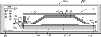
- FIG. 5 is a plan view of an example of the radiation detector of the embodiment seen from the first surface side of the base material.
- FIG. 2 is a cross-sectional view taken along the line AA of the radiation detector shown in FIG. It is sectional drawing BB of the radiation detector shown in FIG.
- It is a schematic diagram for demonstrating the operation of the stress neutral plane adjustment member. It is a schematic diagram for demonstrating the operation of the stress neutral plane adjustment member. It is a schematic diagram for demonstrating the operation of the stress neutral plane adjustment member. It is a figure explaining an example of the manufacturing method of the radiation detector of an embodiment.
- FIG. 5 is a plan view of an example of the radiation detector of Modification 3 as viewed from the first surface side of the base material.
- FIG. 5 is a cross-sectional view taken along the line AA of an example of the radiation detector of the modified example 4.
- FIG. 5 is a cross-sectional view taken along the line AA of an example of the radiation detector of the modified example 5.
- Another example of the radiation detector is a plan view seen from the first surface side of the base material.
- FIG. 5 is a cross-sectional view taken along the line AA of another example of a radiation detector. It is sectional drawing of an example of the radiation imaging apparatus of embodiment which is housed in a housing. It is sectional drawing of another example of the radiation imaging apparatus of embodiment which is housed in a housing. It is sectional drawing of another example of the radiation imaging apparatus of embodiment which is housed in a housing.
- the radiation detector of the present embodiment has a function of detecting radiation transmitted through a subject and outputting image information representing a radiation image of the subject.
- the radiation detector of the present embodiment includes a sensor substrate and a conversion layer that converts radiation into light (see FIG. 2, sensor substrate 12 and conversion layer 14 of the radiation detector 10).
- the sensor substrate 12 of this embodiment is an example of the substrate of the present disclosure.
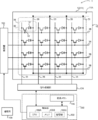
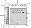
- FIG. 1 is a block diagram showing an example of a configuration of a main part of an electrical system in the radiation imaging apparatus of the present embodiment.
- the radiation imaging device 1 of the present embodiment includes a radiation detector 10, a control unit 100, a drive unit 102, a signal processing unit 104, an image memory 106, and a power supply unit 108.
- the radiation detector 10 includes a sensor substrate 12 and a conversion layer (see FIG. 2) that converts radiation into light.
- the sensor substrate 12 includes a flexible base material 11 and a plurality of pixels 30 provided on the first surface 11A of the base material 11. In the following, the plurality of pixels 30 may be simply referred to as “pixel 30”.
- each pixel 30 of the present embodiment has a sensor unit 34 that generates and accumulates electric charges according to the light converted by the conversion layer, and a switching element 32 that reads out the electric charges accumulated by the sensor unit 34.
- a thin film transistor TFT: Thin Film Transistor
- the switching element 32 will be referred to as "TFT32".
- the sensor unit 34 and the TFT 32 are formed, and a layer in which the pixels 30 are formed on the first surface 11A of the base material 11 is provided as a flattened layer.
- the pixel 30 corresponds to the pixel region 35 of the sensor substrate 12 in one direction (scanning wiring direction corresponding to the horizontal direction in FIG. 1, hereinafter also referred to as “row direction”) and an intersection direction with respect to the row direction (corresponding to the vertical direction in FIG. 1). It is arranged in a two-dimensional manner along the signal wiring direction (hereinafter also referred to as "row direction").
- row direction the arrangement of the pixels 30 is shown in a simplified manner. For example, 1024 pixels ⁇ 1024 pixels 30 are arranged in the row direction and the column direction.
- the radiation detector 10 is provided with a plurality of scanning wires 38 for controlling the switching state (on and off) of the TFT 32, which are provided for each row of the pixel 30, and for each column of the pixel 30.
- a plurality of signal wirings 36 from which the electric charge accumulated in the sensor unit 34 is read out are provided so as to intersect each other.
- Each of the plurality of scanning wires 38 is connected to the drive unit 102 via the cable 112A (see FIG. 2) to drive the TFT 32 output from the drive unit 102 to control the switching state.
- a signal flows through each of the plurality of scanning wires 38.
- each of the plurality of signal wirings 36 is connected to the signal processing unit 104 via the cable 112B (see FIG. 2), so that the electric charge read from each pixel 30 is signal-processed as an electric signal. It is output to unit 104.
- the signal processing unit 104 generates and outputs image data corresponding to the input electric signal.
- a control unit 100 which will be described later, is connected to the signal processing unit 104, and the image data output from the signal processing unit 104 is sequentially output to the control unit 100.
- An image memory 106 is connected to the control unit 100, and image data sequentially output from the signal processing unit 104 is sequentially stored in the image memory 106 under the control of the control unit 100.
- the image memory 106 has a storage capacity capable of storing a predetermined number of image data, and each time a radiographic image is taken, the image data obtained by the taking is sequentially stored in the image memory 106.
- the control unit 100 includes a CPU (Central Processing Unit) 100A, a memory 100B including a ROM (Read Only Memory) and a RAM (Random Access Memory), and a non-volatile storage unit 100C such as a flash memory.
- a CPU Central Processing Unit
- a memory 100B including a ROM (Read Only Memory) and a RAM (Random Access Memory)
- a non-volatile storage unit 100C such as a flash memory.
- An example of the control unit 100 is a microcomputer or the like.
- the control unit 100 controls the overall operation of the radiographic imaging apparatus 1.
- the image memory 106, the control unit 100, and the like are formed on the control board 110.
- a common wiring 39 is provided in the wiring direction of the signal wiring 36 in order to apply a bias voltage to each pixel 30.
- the power supply unit 108 supplies electric power to various elements and circuits such as the control unit 100, the drive unit 102, the signal processing unit 104, the image memory 106, and the power supply unit 108.
- various elements and circuits such as the control unit 100, the drive unit 102, the signal processing unit 104, the image memory 106, and the power supply unit 108.
- the wiring for connecting the power supply unit 108 and various elements and various circuits is omitted.
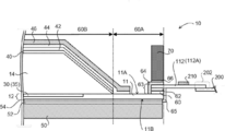
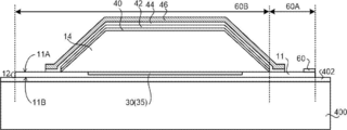
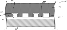
- FIG. 2 is an example of a plan view of the radiation detector 10 of the present embodiment as viewed from the first surface 11A side of the base material 11.
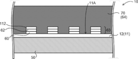
- FIG. 3A is an example of a cross-sectional view taken along the line AA of the radiation detector 10 in FIG.
- FIG. 3B is an example of a sectional view taken along line BB of the radiation detector 10 in FIG.
- the first surface 11A of the base material 11 is divided into a terminal region 60A in which the terminal portion 60 is provided and a terminal region outside 60B in which the terminal portion 60 is not provided.
- the pixel region 35 provided with the above-mentioned pixel 30 is provided in the terminal region outer 60B.
- the base material 11 is a resin sheet that has flexibility and contains, for example, a plastic such as PI (PolyImide: polyimide).
- the thickness of the base material 11 is such that desired flexibility can be obtained depending on the hardness of the material, the size of the sensor substrate 12 (the area of the first surface 11A or the second surface 11B), and the like. Good.
- PI PolyImide: polyimide
- the gravity of the base material 11 is 2 mm at a position 10 cm away from the fixed side.
- the base material 11 hangs down (becomes lower than the height of the fixed side).
- a thickness of 5 ⁇ m to 125 ⁇ m may be used, and a thickness of 20 ⁇ m to 50 ⁇ m is more preferable.
- the base material 11 has a property that can withstand the production of the pixel 30, and in the present embodiment, it has a property that can withstand the production of an amorphous silicon TFT (a-Si TFT).
- a-Si TFT amorphous silicon TFT
- the coefficient of thermal expansion (CTE: Coefficient of Thermal Expansion) at 300 ° C. to 400 ° C. is about the same as that of an amorphous silicon (Si) wafer (for example, ⁇ 5 ppm / K). It is preferably 20 ppm / K or less.
- the heat shrinkage rate of the base material 11 it is preferable that the heat shrinkage rate at 400 ° C. is 0.5% or less when the thickness is 25 ⁇ m.
- the elastic modulus of the base material 11 does not have a transition point possessed by a general PI in the temperature range between 300 ° C. and 400 ° C., and the elastic modulus at 500 ° C. is preferably 1 GPa or more.
- the base material 11 of the present embodiment has a fine particle layer containing inorganic fine particles having an average particle diameter of 0.05 ⁇ m or more and 2.5 ⁇ m or less and absorbing backscattered rays in order to suppress backscattered rays by itself. It is preferable to have.
- inorganic fine particles in the case of the resinous base material 11, it is preferable to use an inorganic material having an atomic number larger than the atoms constituting the organic material which is the base material 11 and 30 or less.
- Specific examples of such fine particles include SiO 2 , which is an oxide of Si having an atomic number of 14, MgO, which is an oxide of Mg having an atomic number of 12, and Al 2 , which is an oxide of Al having an atomic number of 13. Examples thereof include O 3 and TiO 2 , which is an oxide of Ti having an atomic number of 22.
- Specific examples of the resin sheet having such characteristics include XENOMAX (registered trademark).
- the above thickness in this embodiment was measured using a micrometer.
- the coefficient of thermal expansion was measured according to JIS K7197: 1991. In the measurement, test pieces were cut out from the main surface of the base material 11 at different angles of 15 degrees, the coefficient of thermal expansion was measured for each of the cut out test pieces, and the highest value was taken as the coefficient of thermal expansion of the base material 11. ..
- the coefficient of thermal expansion is measured at intervals of 10 ° C. from -50 ° C to 450 ° C in each of the MD (Machine Direction) direction and the TD (Transverse Direction) direction, and (ppm / ° C) is converted to (ppm / K). did.
- the coefficient of thermal expansion was measured using a TMA4000S device manufactured by MAC Science, with a sample length of 10 mm, a sample width of 2 mm, an initial load of 34.5 g / mm2, a heating rate of 5 ° C./min, and an atmosphere of argon. And said.
- the base material 11 having the desired flexibility is not limited to a resin sheet or the like.
- the base material 11 may be a glass substrate or the like having a relatively thin thickness.
- a size having a side of about 43 cm has flexibility if the thickness is 0.3 mm or less, so that the thickness is 0.3 mm or less. Any glass substrate may be desired.
- the plurality of pixels 30 are provided in a part of the inside of 60B outside the terminal region on the first surface 11A of the base material 11. Further, in the sensor substrate 12 of the present embodiment, the pixel 30 is not provided in the terminal region 60A on the first surface 11A of the substrate 11. In the present embodiment, the region provided with the pixels 30 on the first surface 11A of the base material 11 is defined as the pixel region 35.
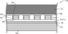
- the conversion layer 14 of the present embodiment covers the pixel region 35.
- a scintillator containing CsI (cesium iodide) is used as an example of the conversion layer 14.
- scintillators include CsI: Tl (cesium iodide added with thallium) and CsI: Na (cesium iodide added with sodium) having an emission spectrum of 400 nm to 700 nm during X-ray irradiation. It is preferable to include it.
- the emission peak wavelength of CsI: Tl in the visible light region is 565 nm.
- an adhesive layer 40, a reflective layer 42, an adhesive layer 44, and a protective layer 46 are provided on the conversion layer 14 of the present embodiment.
- the adhesive layer 40 covers the entire surface of the conversion layer 14.
- the adhesive layer 40 has a function of fixing the reflective layer 42 on the conversion layer 14.
- the adhesive layer 40 preferably has light transmittance.
- an acrylic adhesive, a hot melt adhesive, and a silicone adhesive can be used as the material of the adhesive layer 40.
- the acrylic pressure-sensitive adhesive include urethane acrylate, acrylic resin acrylate, and epoxy acrylate.
- the hot melt adhesive include EVA (ethylene / vinyl acetate copolymer resin), EAA (ethylene / acrylic acid copolymer resin), EEA (ethylene-ethylacrylate copolymer resin), and EMMA (ethylene-methacryl).
- Thermoplastics such as methyl acid copolymer) can be mentioned.
- the thickness of the adhesive layer 40 is preferably 2 ⁇ m or more and 7 ⁇ m or less.
- the thickness of the adhesive layer 40 is preferably 2 ⁇ m or more and 7 ⁇ m or less.
- the reflective layer 42 covers the entire surface of the adhesive layer 40.
- the reflective layer 42 has a function of reflecting the light converted by the conversion layer 14.
- the reflective layer 42 is preferably made of an organic material.
- white PET Polyethylene terephthalate
- TiO 2 , Al 2 O 3 foamed white PET
- polyester-based highly reflective sheet polyester-based highly reflective sheet
- specular reflective aluminum and the like can be used as the material of the reflective layer 42.
- White PET is obtained by adding a white pigment such as TiO 2 or barium sulfate to PET, and foamed white PET is white PET having a porous surface.
- the polyester-based high-reflection sheet is a sheet (film) having a multilayer structure in which a plurality of thin polyester sheets are stacked.
- the thickness of the reflective layer 42 is preferably 10 ⁇ m or more and 40 ⁇ m or less.
- the adhesive layer 44 covers the entire surface of the reflective layer 42.
- the end of the adhesive layer 44 extends to the surface of the sensor substrate 12. That is, the adhesive layer 44 is adhered to the sensor substrate 12 at its end.
- the adhesive layer 44 has a function of fixing the reflective layer 42 and the protective layer 46 to the conversion layer 14.
- the material of the adhesive layer 44 the same material as the material of the adhesive layer 40 can be used, but the adhesive force of the adhesive layer 44 is preferably larger than that of the adhesive layer 40.
- the protective layer 46 is provided so as to cover the entire conversion layer 14 and its end portion to cover a part of the sensor substrate 12.
- the protective layer 46 functions as a moisture-proof film that prevents water from entering the conversion layer 14.
- PET PET
- PPS PolyPhenylene Sulfide: polyphenylene sulfide
- OPP Oriented PolyPropylene: biaxially stretched polypropylene film
- PEN PolyEthylene Naphthalate: polyethylene naphthalate
- PI polyEthylene Naphthalate
- PI polyethylene naphthalate
- Membranes and parylene registered trademark
- a laminated film of a resin film and a metal film may be used as the protective layer 46. Examples of the laminated film of the resin film and the metal film include a sheet of Alpet (registered trademark).
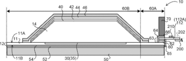
- the antistatic layer 54 and the adhesive 52 are interposed on the second surface 11B side of the base material 11 in the sensor substrate 12 of the radiation detector 10 of the present embodiment.
- the reinforcing member 50 is provided.
- the reinforcing member 50 has a function of reinforcing the strength of the base material 11.
- the reinforcing member 50 of the present embodiment has higher flexural rigidity than the base material 11, and the dimensional change (deformation) with respect to the force applied in the direction perpendicular to the surface facing the conversion layer 14 is the second of the base material 11. It is smaller than the dimensional change with respect to the force applied in the direction perpendicular to the surface 11B of.
- the bending rigidity of the reinforcing member 50 is preferably 100 times or more the bending rigidity of the base material 11.
- the thickness of the reinforcing member 50 of the present embodiment is thicker than the thickness of the base material 11.
- the thickness of the reinforcing member 50 is preferably about 0.2 mm to 0.25 mm.
- the reinforcing member 50 preferably has a higher bending rigidity than the base material 11 from the viewpoint of suppressing the bending of the base material 11.
- the flexural modulus is lowered, the flexural rigidity is also lowered, and in order to obtain the desired flexural rigidity, the thickness of the reinforcing member 50 must be increased, and the thickness of the entire radiation detector 10 is increased. ..
- the thickness of the reinforcing member 50 tends to be relatively thick when trying to obtain a bending rigidity exceeding 140000 Pacm 4 . Therefore, considering that appropriate rigidity can be obtained and the thickness of the entire radiation detector 10 is taken into consideration, the material used for the reinforcing member 50 is more preferably having a flexural modulus of 150 MPa or more and 2500 MPa or less. Further, the bending rigidity of the reinforcing member 50 is preferably 540 Pacm 4 or more and 140000 Pacm 4 or less.
- the coefficient of thermal expansion of the reinforcing member 50 of the present embodiment is preferably close to the coefficient of thermal expansion of the material of the conversion layer 14, and more preferably the coefficient of thermal expansion of the reinforcing member 50 with respect to the coefficient of thermal expansion of the conversion layer 14.
- the ratio (coefficient of thermal expansion of the reinforcing member 50 / coefficient of thermal expansion of the conversion layer 14) is preferably 0.5 or more and 2 or less.
- the coefficient of thermal expansion of such a reinforcing member 50 is preferably 30 ppm / K or more and 80 ppm / K or less.
- the coefficient of thermal expansion is 50 ppm / K.
- the material of the reinforcing member 50 is more preferably a material containing at least one of PET and PC.
- the reinforcing member 50 preferably contains a material having a yield point.
- the "yield point” refers to a phenomenon in which the stress drops suddenly when the material is pulled, and the strain does not increase on the curve showing the relationship between the stress and the strain.
- the point of increase which refers to the top of the stress-strain curve when a tensile strength test is performed on a material.
- Resins having a yield point generally include resins that are hard and sticky, and resins that are soft and sticky and have moderate strength. Examples of the hard and sticky resin include PC and the like. Further, examples of the resin having a softness, a strong stickiness, and a medium strength include polypropylene and the like.
- the reinforcing member 50 of this embodiment is a substrate made of plastic.
- the plastic used as the material of the reinforcing member 50 is preferably a thermoplastic resin for the reasons described above, and is preferably PC, PET, styrene, acrylic, polyacetase, nylon, polypropylene, ABS (Acrylonitrile Butadinee Styrene), engineering plastic, and polyphenylene ether. At least one of.
- the reinforcing member 50 is preferably at least one of polypropylene, ABS, engineering plastic, PET, and polyphenylene ether, and more preferably at least one of styrene, acrylic, polyacetase, and nylon. , PC and PET are more preferable.
- a plurality of terminal portions 60 are provided in the terminal region 60A of the radiation detector 10 of the present embodiment.
- the terminal region 60A is provided on each of the two intersecting sides of the rectangular sensor substrate 12 (base material 11).
- the terminal region 60A refers to a region on the first surface 11A of the base material 11 where a plurality of terminal portions 60 are provided, and includes at least a region where the terminal portions 60 are in contact with the first surface 11A.
- the terminal region includes at least the region where the terminal portion 60 is in contact with the first surface 11A over the entire side of the sensor substrate 12 (base material 11) where the terminal portion 60 is provided. It is called 60A.
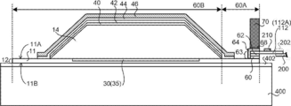
- a cable 112 is electrically connected to each of the terminal portions 60 provided in the terminal region 60A of the base material 11.
- the cable 112A is thermocompression-bonded to each of a plurality of (8 in FIG. 2) terminal portions 60 provided on one side of the base material 11.
- the cable 112A is a so-called COF (Chip on Film), and the cable 112A is equipped with a drive IC (Integrated Circuit) 210.
- the drive IC 210 is connected to a plurality of signal lines (see FIG. 4, signal line 113) included in the cable 112A.
- the cable 112A and the cable 112B described later are generically referred to without distinction, they are simply referred to as "cable 112".
- the other end of the cable 112A which is electrically connected to the terminal portion 60 of the sensor board 12, and the other end on the opposite side, is electrically connected to the connection area 202 of the drive board 200.
- a plurality of signal lines included in the cable 112A are thermocompression-bonded to the drive board 200, so that the circuits and elements mounted on the drive board 200 and the like are formed. (Not shown) is connected.
- the method of electrically connecting the drive board 200 and the cable 112A is not limited to this embodiment, and may be, for example, electrically connected by a connector. Examples of such a connector include a ZIF (Zero Insert Force) structure connector and a Non-ZIF structure connector.
- the drive board 200 of this embodiment is a flexible PCB (Printed Circuit Board) board, which is a so-called flexible board.
- the circuit components (not shown) mounted on the drive board 200 are components mainly used for processing digital signals (hereinafter, referred to as “digital components”).
- Digital components tend to have a relatively smaller area (size) than analog components, which will be described later.
- Specific examples of digital components include digital buffers, bypass capacitors, pull-up / pull-down resistors, damping resistors, EMC (Electro Magnetic Compatibility) countermeasure chip components, power supply ICs, and the like.
- the drive substrate 200 does not necessarily have to be a flexible substrate, may be a non-flexible rigid substrate, or may use a rigid flexible substrate.
- the drive unit 102 is realized by the drive board 200 and the drive IC 210 mounted on the cable 112A.
- the drive IC 210 includes various circuits and elements that realize the drive unit 102, which are different from the digital components mounted on the drive board 200.
- the cable 112B is electrically connected to each of the plurality of (8 in FIG. 2) terminal portions 60 provided on the side where the cable 112A intersects one side of the electrically connected base material 11.
- the cable 112B is a so-called COF (Chip on Film), and the cable 112B is equipped with a signal processing IC 310.
- the signal processing IC 310 is connected to a plurality of signal lines (see FIG. 4, signal line 113) included in the cable 112B.
- the other end of the cable 112B which is electrically connected to the terminal portion 60 of the sensor board 12, and the other end on the opposite side, is electrically connected to the connection area 302 of the signal processing board 300.
- a plurality of signal lines included in the cable 112B are heat-bonded to the signal processing board 300 to form a circuit mounted on the signal processing board 300 and a circuit. It is connected to an element or the like (not shown).
- the method of electrically connecting the signal processing board 300 and the cable 112B is not limited to this embodiment, and may be, for example, electrically connected by a connector.
- Examples of such a connector include a ZIF (Zero Insert Force) structure connector and a Non-ZIF structure connector.
- the method of electrically connecting the cable 112A and the drive board 200 and the method of electrically connecting the cable 112B and the signal processing board 300 may be the same or different.
- the cable 112A and the drive board 200 may be electrically connected by thermocompression bonding, and the cable 112B and the signal processing board 300 may be electrically connected by a connector.
- the signal processing board 300 of the present embodiment is a flexible PCB board like the drive board 200 described above, and is a so-called flexible board.
- the circuit components (not shown) mounted on the signal processing board 300 are components mainly used for processing analog signals (hereinafter, referred to as “analog components”). Specific examples of analog components include a charge amplifier, an analog-to-digital converter (ADC), a digital-to-analog converter (DAC), a power supply IC, and the like. Further, the circuit component of the present embodiment also includes a coil around a power supply having a relatively large component size and a large-capacity capacitor for smoothing.
- the signal processing substrate 300 does not necessarily have to be a flexible substrate, may be a non-flexible rigid substrate, or may use a rigid flexible substrate.
- the signal processing unit 104 is realized by the signal processing board 300 and the signal processing IC 310 mounted on the cable 112B.
- the signal processing IC 310 includes various circuits and elements that realize the signal processing unit 104, which are different from the analog components mounted on the signal processing board 300.
- a plurality of drive boards 200 and signal processing boards 300 are provided (two each in FIG. 2), but the number of drive boards 200 and signal processing boards 300 is the same. It is not limited to the embodiment. For example, either one of the drive board 200 and the signal processing board 300 may be used as one board.
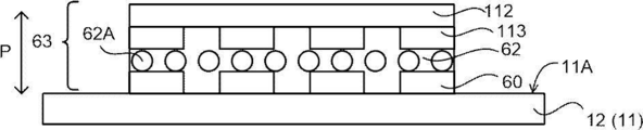
- the cable 112 is thermocompression bonded to the terminal portion 60 via the connection layer 62, so that the cable 112 is electrically attached to the terminal portion 60.
- FIGS. 3A and 3B Connected to. 3A and 3B are diagrams showing an example of the structure relating to the electrical connection between the cable 112A and the radiation detector 10, but the cable 112B and the radiation detector 10 of the present embodiment are electrically connected. The structure relating to the above is also the same as that illustrated in FIGS. 3A and 3B.
- connection layer 62 has a function of electrically connecting the terminal portion 60 and the cable 112.
- Examples of the connecting layer 62 include an anisotropic conductive film, and ACF (Anisotropic Conductive Film) in which conductive particles (see FIG. 4A and conductive particles 62A) are dispersed in an adhesive that is cured by heat is used. be able to.
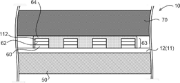
- the first surface 11A side of the base material 11 in the laminated body 63 in which the terminal portion 60, the connecting layer 62, and the cable 112 are laminated is covered with the reinforcing member 64.
- the side surface of the laminate in which the terminal portion 60, the connection layer 62, and the cable 112 are laminated and the side surface of the base material 11 are covered with the reinforcing member 65.
- the reinforcing member 64 and the reinforcing member 65 have a function of strengthening the electrical connection between the terminal portion 60 and the cable 112. Further, the reinforcing member 64 and the reinforcing member 65 of the present embodiment have moisture resistance.
- the reinforcing member 64 and the reinforcing member 65 for example, a moisture-proof insulating film can be used, and Tuffy (registered trademark) or the like, which is a moisture-proof insulating material for FPD (Flat Panel Display), can be used.
- Tuffy registered trademark
- FPD Flat Panel Display
- Each of the reinforcing member 64 and the reinforcing member 65 may be a member made of the same material or a member made of a different material.
- a stress neutral surface adjusting member 70 is provided on the laminated body 63 covered with the reinforcing member 64 via an adhesive 66.
- the stress neutral surface adjusting member 70 is a laminated body of the stress neutral surface 71 (see FIG. 5, details described later) in the region where the laminated body 63 of the radiation detector 10 is provided when the radiation detector 10 is bent. The position of 63 with respect to the stacking direction P is adjusted.
- PET is used as an example of the stress neutral surface adjusting member 70, and white PET, foamed white PET, or the like may be used.
- other examples of the stress neutral plane adjusting member 70 include organic films such as PC, LDPE (Low Density Polyethylene), PPS, OPP, PEN, and PI.
- the stress neutral surface adjusting member 70 preferably has a higher bending rigidity than the base material 11 from the viewpoint of suppressing the bending of the base material 11.
- the flexural rigidity referred to here means the difficulty of bending, and the higher the bending rigidity, the more difficult it is to bend.
- the thickness of the stress neutral plane adjusting member 70 As the flexural modulus decreases, the flexural rigidity also decreases, and in order to obtain the desired flexural rigidity, the thickness of the stress neutral plane adjusting member 70 must be increased, and the thickness of the entire radiation detector 10 increases. It ends up.
- the material used for the stress neutral plane adjusting member 70 preferably has a flexural modulus of 150 MPa or more and 2500 MPa or less. Further, the flexural rigidity of the stress neutral plane adjusting member 70 is preferably 540 Pacm 4 or more and 140000 Pacm 4 or less.
- the coefficient of thermal expansion of the stress neutral surface adjusting member 70 of the present embodiment is preferably close to the coefficient of thermal expansion of the material of the conversion layer 14, more preferably the stress neutral surface with respect to the coefficient of thermal expansion of the conversion layer 14.
- the ratio of the coefficient of thermal expansion of the adjusting member 70 (the coefficient of thermal expansion of the stress neutral plane adjusting member 70 / the coefficient of thermal expansion of the conversion layer 14) is preferably 0.5 or more and 4 or less.
- the coefficient of thermal expansion of the stress neutral surface adjusting member 70 is preferably 30 ppm / K or more and 200 ppm / K or less. For example, when the conversion layer 14 is made of CsI: Tl, the coefficient of thermal expansion is 50 ppm / K.
- LDPE having a coefficient of thermal expansion of 100 ppm / K to 200 ppm / K
- PVC having a coefficient of thermal expansion of 60 ppm / K to 80 ppm / K
- acrylic having a coefficient of thermal expansion of 70 ppm / K to 80 ppm / K
- thermal expansion PET having a coefficient of 65 ppm / K to 70 ppm / K
- PC having a coefficient of thermal expansion of 65 ppm / K
- Teflon registered trademark
- the material of the stress neutral plane adjusting member 70 is more preferably a material containing at least one of PET, PC, and LDPE.
- the stress neutral surface adjusting member 70 has other functions such as an antistatic function and a moisture-proof function in addition to the function of adjusting the position of the stress neutral surface.
- FIGS. 4A, 4B, and 5 The operation of the stress neutral plane adjusting member 70 in the radiation detector 10 of the present embodiment will be described with reference to FIGS. 4A, 4B, and 5. Note that, in FIGS. 4A, 4B, and 5, for simplification, only the configuration of the radiation detector 10 necessary for explaining the operation of the stress neutral plane adjusting member 70 is schematically shown.
- the connecting layer 62 contains the conductive particles 62A.
- the conductive particles 62A By arranging the conductive particles 62A between the terminal portion 60 provided on the first surface 11A of the base material 11 and the signal line 113, the terminal portion 60 and the signal line 113 of the cable 112 are electrically connected to each other. Be connected.
- FIG. 4B shows a state in which the stress neutral plane adjusting member 70 of the present embodiment is not provided.
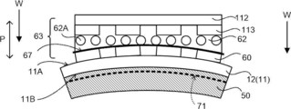
- the reinforcing member 50 is provided on the second surface 11B of the sensor substrate 12 (base material 11), for example, when a load W is applied in the stacking direction of the laminated body 63, or when a film is applied.
- the sensor substrate 12 and the reinforcing member 50 are bent by the action of stress.
- the position of the stress neutral surface 71 generated when the sensor substrate 12 and the reinforcing member 50 are bent is in the stacking direction P.
- the stress neutral surface 71 is located in the reinforcing member 50.
- the “stress neutral surface 71” refers to a surface in which the sensor substrate 12 and the reinforcing member 50 do not expand or contract even when bent, in other words, a surface in a direction intersecting the stacking direction P. At the stress neutral plane 71, the stress becomes zero.
- the terminal portion 60 since the position of the stress neutral surface 71 is relatively far from the interface 67, the terminal portion 60 also bends according to the bending of the sensor substrate 12 and the reinforcing member 50. Specifically, the interface 67 bends. Therefore, as shown in FIG. 4B, the terminal portion 60 and the conductive particles 62A are in a non-contact state, and the electrical connection between the terminal portion 60 and the cable 112 is cut off. When the electrical connection between the terminal portion 60 and the cable 112 is broken, the image quality of the radiation image obtained by the radiation detector 10 may deteriorate, and for example, so-called line defects may occur.
- the stress neutral surface adjusting member 70 is provided on the laminated body 63, the position of the stress neutral surface 71 is higher than that in the case where the stress neutral surface adjusting member 70 is not provided. Also moves to the laminate 63 side.
- the distance between the stress neutral surface 71 and the interface 67 is larger than that when the stress neutral surface adjusting member 70 is not provided (in the case of FIG. 4B). Can also be made smaller.
- the stress neutral surface adjusting member 70 is provided, the difference between the position of the stress neutral surface 71 and the position of the interface 67 is larger than that when the stress neutral surface adjusting member 70 is not provided (in the case of FIG. 4B). Can also be made smaller.
- the stress neutral surface 71 By moving the position of the stress neutral surface 71 closer to the position of the interface 67, the stress at the interface 67 when the sensor substrate 12 and the reinforcing member 50 are bent can be reduced, so that the terminal portion 60 and the connecting layer 62 It becomes difficult for the conductive particles 62A to be in a non-contact state. Therefore, the electrical connection between the terminal portion 60 and the cable 112 is less likely to be disconnected.
- the position of the stress neutral surface 71 is preferably a position in the laminated body 63.
- the inside of the laminated body 63 in the present embodiment is an example within the predetermined range of the present disclosure.
- the position of the stress neutral surface 71 and the position of the interface 67 coincide with each other.
- the stress at the interface 67 can be set to 0, so that the terminal portion 60 and the conductive particles 62A of the connecting layer 62 are less likely to be in a non-contact state. Become. Therefore, the electrical connection between the terminal portion 60 and the cable 112 is less likely to be disconnected.
- the stress neutral surface adjusting member 70 is provided with the terminal portion 60, the connecting layer 62, and the cable 112 on the first surface 11A of the sensor substrate 12 (base material 11).
- the stress neutral surface 71 By providing the stress neutral surface 71 on the laminated body 63, the position of the stress neutral surface 71 in the stacking direction P can be adjusted in the vicinity of the interface 67.
- the stress generated at the interface 67 can be brought close to 0, so that the electricity between the terminal portion 60 and the cable 112 can be reduced to zero. Connection is hard to be disconnected.
- the thickness of the stress neutral surface adjusting member 70 is determined according to an acceptable range as the position of the stress neutral surface 71 from the interface 67. As an acceptable range, for example, the inside of the laminated body 63 can be mentioned as described above.
- the specific thickness of the stress neutral surface adjusting member 70 is determined according to the ease with which the conductive particles 62A of the connecting layer 62 and the terminal portion 60 are in a non-contact state, the degree of expected bending, and the like. .. For example, it is preferable that the thicker the reinforcing member 50 is, the thicker the stress neutral surface adjusting member 70 is.
- the base material 11 is formed on the support 400 such as a glass substrate which is thicker than the base material 11 via the release layer 402.
- the support 400 such as a glass substrate which is thicker than the base material 11 via the release layer 402.
- a sheet to be the base material 11 is attached onto the support 400.
- the second surface 11B of the base material 11 is in contact with the release layer 402.
- the method of forming the base material 11 is not limited to this embodiment, and may be, for example, a form in which the base material 11 is formed by a coating method.
- the pixel 30 is formed on the first surface 11A of the base material 11 outside the terminal region 60B.
- the pixels 30 are formed on the first surface 11A of the base material 11 via an undercoat layer (not shown) using SiN or the like.
- the conversion layer 14 is formed on the layer on which the pixel 30 is formed (hereinafter, simply referred to as "pixel 30").
- the CsI conversion layer 14 is formed as columnar crystals directly on the sensor substrate 12 by a vapor deposition method such as a vacuum deposition method, a sputtering method, and a CVD (Chemical Vapor Deposition) method.
- the side of the conversion layer 14 in contact with the pixel 30 is the growth direction base point side of the columnar crystal.
- the conversion layer 14 can be formed on the sensor substrate 12 by a method different from that of the present embodiment. For example, prepare an aluminum plate or the like on which CsI is vapor-deposited by a vapor deposition method, and attach the side of the CsI that is not in contact with the aluminum plate and the pixel 30 of the sensor substrate 12 with an adhesive sheet or the like. As a result, the conversion layer 14 may be formed on the sensor substrate 12. In this case, it is preferable that the entire conversion layer 14 including the aluminum plate is covered with the protective layer 46 and bonded to the pixels 30 of the sensor substrate 12. In this case, the side of the conversion layer 14 in contact with the pixel 30 is the tip side in the growth direction of the columnar crystal.
- GOS Ga 2 O 2 S: Tb
- the conversion layer 14 may be used as the conversion layer 14 instead of CsI.
- a sheet in which GOS is dispersed in a binder such as resin is prepared by bonding a support formed of white PET or the like with an adhesive layer or the like, and the GOS support is not bonded.
- the conversion layer 14 can be formed on the sensor substrate 12 by bonding the side and the pixels 30 of the sensor substrate 12 with an adhesive sheet or the like.
- CsI is used for the conversion layer 14 the conversion efficiency from radiation to visible light is higher than when GOS is used.
- a reflective layer 42 is provided via the adhesive layer 40 on the conversion layer 14 formed on the sensor substrate 12, and a protective layer 46 is further provided via the adhesive layer 44. Further, the terminal portion 60 is formed in the terminal region 60A of the first surface 11A of the base material 11.
- the cable 112 is thermocompression-bonded to the terminal portion 60 via the connection layer 62 to electrically connect the terminal portion 60 and the connection layer 62. Further, the reinforcing member 64 covers the laminated body 63.
- a stress neutral surface adjusting member 70 is provided on the laminated body 63 covered with the reinforcing member 64 by the adhesive 66.
- the sensor substrate 12 in which the cable 112 is electrically connected to the conversion layer 14 and the terminal portion 60 is peeled off from the support 400 to bring it into the state shown in FIG. 6D. ..
- any of the four sides of the sensor substrate 12 (base material 11) is set as the starting point of peeling, and the sensor substrate 12 is gradually peeled off from the support 400 from the starting point toward the opposite side. , Perform mechanical peeling.
- the reinforcing member is attached to the second surface 11B of the base material 11 via the antistatic layer 54 and the adhesive 52. 50 is formed. In this way, the radiation detector 10 of the present embodiment is manufactured.
- the radiation detector 10 of this embodiment may be in the form shown in the following modifications 1 to 5, for example.
- each of the modified examples 1 to 5 may be appropriately combined.
- FIG. 7 shows an example of a cross-sectional view of the radiation detector 10 of this modified example, which corresponds to the cross-sectional view taken along the line BB of the radiation detector 10 shown in FIG. 3B.
- the description of the pressure-sensitive adhesive 52, the antistatic layer 54, and the pressure-sensitive adhesive 66 is omitted.
- the reinforcing member 64 covered each laminated body 63, in other words, each terminal portion 60, but as shown in FIG. 7, in the radiation detector 10 of this modified example.
- the reinforcing member 64 covers the whole of each of the plurality of laminated bodies 63. Therefore, the space between the laminated bodies 63 is filled with the reinforcing member 64. Therefore, in the radiation detector 10 of this modified example, the plurality of laminated bodies 63 are integrally fixed to the sensor substrate 12.
- the number of laminated bodies 63 covered by the reinforcing member 64 is not particularly limited.
- the drive substrate 200 or the signal processing substrate 300 electrically connected by the cable 112 may be bundled together with the same laminated body 63 and covered with the reinforcing member 64.
- the laminated body 63 formed by all the terminal portions 60 provided on one side of the sensor substrate 12 (base material 11) may be collectively covered with the reinforcing member 64.
- Modification 2 8A and 8B show an example of a cross-sectional view of the radiation detector 10 of this modified example, which corresponds to the cross-sectional view taken along the line BB of the radiation detector 10 shown in FIG. 3B. Note that in FIGS. 8A and 8B, the description of the pressure-sensitive adhesive 52, the antistatic layer 54, and the pressure-sensitive adhesive 66 is omitted.
- the stress neutral plane adjusting member 70 fills the space between the laminated bodies 63 covered with the reinforcing member 64, and is stress neutral.
- the surface adjusting member 70 reaches the first surface 11A of the sensor substrate 12 (base material 11).
- the stress neutral surface adjusting member 70 that reaches the first surface 11A of the base material 11 fills the space between the laminated bodies 63, so that the stress neutral surface adjusting member 70 causes the terminal portion 60 and the terminal portion 60.
- the electrical connection of the cable 112 is strengthened.
- the stress neutral surface adjusting member 70 may be put together for each of the plurality of laminated bodies 63 to cover the whole without providing the reinforcing member 64.
- the stress neutral plane adjusting member 70 is not limited to the member made of the above-mentioned material, and may be a member made of the same material as the reinforcing member 64. That is, in the case of the form shown in FIG. 8B, the reinforcing member 64 may be used as the stress neutral plane adjusting member 70.
- FIG. 9 shows an example of a plan view of the radiation detector 10 of this modified example, which corresponds to the plan view of the radiation detector 10 shown in FIG. 2.
- a stress neutral plane adjusting member 70 was provided for each side of the sensor substrate 12 (base material 11) corresponding to the terminal region 60A.
- the stress neutral plane adjusting member 70 is a laminate 63 corresponding to the cable 112A (see FIG. 3B, etc.) and a laminate 63 corresponding to the cable 112B (FIG. 3B, etc.). (See) It was provided for each.
- the stress neutral plane adjusting member 70 may be provided over at least one or more laminated bodies 63 (terminal portions 60), and the number thereof is not limited.
- the stress neutral plane adjusting member 70 may be provided for each laminated body 63 (terminal portion 60).
- the stress neutral plane adjusting member 70 does not have to be provided in the entire terminal region 60A. Further, the stress neutral surface adjusting member 70 may not be provided on the entire upper surface of each laminated body 63.
- FIG. 10 shows an example of a cross-sectional view of the radiation detector 10 of this modified example, which corresponds to the cross-sectional view taken along the line AA of the radiation detector 10 shown in FIG. 3A.
- a reinforcing layer 48 is further provided on the conversion layer 14 covered with the protective layer 46.
- the reinforcing layer 48 has a higher bending rigidity than the base material 11, and the dimensional change (deformation) with respect to the force applied in the direction perpendicular to the surface facing the conversion layer 14 is caused to the first surface 11A of the base material 11. On the other hand, it is smaller than the dimensional change with respect to the force applied in the vertical direction. Further, the thickness of the reinforcing layer 48 of this modified example is thicker than the thickness of the base material 11.
- the preferred characteristics of the reinforcing layer 48 are the same as those of the reinforcing layer 48 described above.
- the reinforcing layer 48 of this modification it is preferable to use a material having a flexural modulus of 150 MPa or more and 2500 MPa or less.
- the reinforcing layer 48 preferably has a higher bending rigidity than the base material 11 from the viewpoint of suppressing the bending of the base material 11. As the flexural modulus decreases, the flexural rigidity also decreases, and in order to obtain the desired flexural rigidity, the thickness of the reinforcing layer 48 must be increased, and the thickness of the entire radiation detector 10 increases. ..
- the material used for the reinforcing layer 48 preferably has a flexural modulus of 150 MPa or more and 2500 MPa or less. Further, the flexural rigidity of the reinforcing layer 48 is preferably 540 Pacm 4 or more and 140000 Pacm 4 or less.
- the coefficient of thermal expansion of the reinforcing layer 48 is preferably close to the coefficient of thermal expansion of the material of the conversion layer 14, and more preferably the ratio of the coefficient of thermal expansion of the reinforcing layer 48 to the coefficient of thermal expansion of the conversion layer 14 (reinforcing layer).
- the coefficient of thermal expansion of 48 / the coefficient of thermal expansion of the conversion layer 14) is preferably 0.5 or more and 2 or less.
- the coefficient of thermal expansion of such a reinforcing layer 48 is preferably 30 ppm / K or more and 80 ppm / K or less.
- the coefficient of thermal expansion is 50 ppm / K.
- examples of the material relatively close to the conversion layer 14 include PVC, acrylic, PET, PC, Teflon (registered trademark) and the like.
- the material of the reinforcing layer 48 is more preferably a material containing at least one of PET and PC. Further, from the viewpoint of elasticity, the reinforcing layer 48 preferably contains a material having a yield point.
- the reinforcing layer 48 of this modification is a substrate made of plastic.
- the plastic used as the material of the reinforcing layer 48 is preferably a thermoplastic resin for the reasons described above, and at least one of PC, PET, styrene, acrylic, polyacetase, nylon, polypropylene, ABS, engineering plastic, and polyphenylene ether can be mentioned. Be done.
- the reinforcing layer 48 is preferably at least one of polypropylene, ABS, engineering plastic, PET, and polyphenylene ether, and more preferably at least one of styrene, acrylic, polyacetase, and nylon. , PC and PET are more preferable.
- the specific characteristics, materials, and the like of the reinforcing layer 48 and the reinforcing member 50 may be the same or different.
- the conversion layer 14 is formed with an inclination that gradually decreases in thickness toward the outer edge thereof.
- the central region of the conversion layer 14 in which the thickness can be regarded as substantially constant when manufacturing errors and measurement errors are ignored is referred to as a central portion.
- an outer peripheral region of the conversion layer 14 having a thickness of, for example, 90% or less of the average thickness of the central portion of the conversion layer 14 is referred to as a peripheral edge portion. That is, the conversion layer 14 has an inclined surface inclined with respect to the sensor substrate 12 at the peripheral edge portion.
- the reinforcing layer 48 of the present modification covers the entire central portion and a part of the peripheral portion of the conversion layer 14. In other words, the outer edge of the reinforcing layer 48 is located on the inclined surface of the peripheral edge of the conversion layer 14.
- the position where the reinforcing layer 48 is provided is not limited to this modification.
- the reinforcing layer 48 may cover the entire conversion layer 14.
- the reinforcing layer 48 is provided in a state of being bent along the inclined portion of the conversion layer 14, but the inclined portion of the conversion layer 14 is formed in a plate shape without bending.
- a space may be provided between the reinforcing layer 48 and the reinforcing layer 48.
- the reinforcing layer 48 and the stress neutral surface adjusting member 70 are separately provided, so that, for example, the stress neutral surface adjusting member 70 is extended to the upper part of the conversion layer 14 to form the reinforcing layer 48.
- the radiation detector 10 is lighter than the case where it also has the function of.
- FIG. 11 shows an example of a cross-sectional view of the radiation detector 10 of this modified example, which corresponds to the cross-sectional view taken along the line AA of the radiation detector 10 shown in FIG. 3A.
- the sensor substrate 12 (base material 11) provided with the conversion layer 14, the laminate 63, and the stress neutral plane adjusting member 70 by the protective film 49. It covers the entire side of the first surface 11A.
- the adhesive layer 57 provides the conversion layer 14 with the protective film 49
- the adhesive layer 72 provides the stress neutral surface adjusting member 70 with the protective film 49. ing.
- the protective film 49 is a film having a moisture-proof function and a relatively thin thickness.
- the thickness is relatively thin as compared with the reinforcing layer 48 in the radiation detector 10 of the modification 4.
- an insulating sheet such as parylene (registered trademark) or polyethylene terephthalate, or a moisture-proof film such as an alpette (registered trademark) sheet is used.
- the protective film 49 may have an antistatic function in place of the moisture-proof function or in addition to the moisture-proof function.
- the stress neutral surface adjusting member 70 since the stress neutral surface adjusting member 70 is connected to the conversion layer 14 by the protective film 49, the stress neutral surface adjusting member 70 adjusts the stress neutral surface 71.
- the function can be improved.
- the radiation detector 10 of each of the above forms includes a sensor substrate 12, a conversion layer 14, a reinforcing member 50, and a stress neutral plane adjusting member 70.
- a plurality of pixels 30 for accumulating charges generated in response to light converted from radiation are formed in the pixel region 35 of the first surface 11A of the flexible base material 11, and the first A terminal portion 60 for electrically connecting the cable 112 is provided in the terminal region 60A of the surface 11A of the surface 1.
- the conversion layer 14 is provided outside the terminal region 60B on the first surface 11A of the base material 11 and converts radiation into light.
- the reinforcing member 50 is provided on the second surface 11B opposite to the first surface 11A of the base material 11 to reinforce the strength of the base material 11.
- the stress neutral plane adjusting member 70 is provided in at least a part corresponding to the terminal region 60A and the terminal region 60A of the cable 112 electrically connected to the terminal portion 60, and the reinforcing member 50 and the sensor substrate 12 are provided. The position of the stress neutral plane 71 in the region corresponding to the terminal portion 60 and the laminated body 63 in which the cable 112 electrically connected to the terminal portion 60 is laminated is adjusted.
- the terminal portion 60 and the cable 112 are provided due to the bending of the sensor substrate 12 and the reinforcing member 50 by providing the reinforcing member 50.
- the electrical connection of the sensor may be easily disconnected.
- the stress neutral surface adjusting member 70 is provided on the laminated body 63, the position of the stress neutral surface 71 can be determined. It can be in the vicinity of the interface 67 where the terminal portion 60 and the conductive particles 62A of the connection layer 62 are in contact with each other. As a result, according to the radiation detector 10 of the present embodiment and each of the above modifications, the stress at the interface 67 can be reduced, so that the terminal portion 60 and the conductive particles 62A of the connection layer 62 are in a non-contact state. It becomes difficult.
- the radiation detector 10 of the present embodiment and each of the above modifications it is possible to easily prevent the electrical connection between the terminal portion 60 and the cable 112 from being disconnected.
- the electrical connection between the terminal portion 60 and the cable 112 is cut even when the sensor substrate 12 and the reinforcing member 50 are bent. Can be suppressed.
- the radiation detector 10 is not limited to the embodiment described in this embodiment and each of the above modifications.
- Each of the stress neutral plane adjusting member 70 provided on the laminated body 63 by 60 may be a member made of the same material or a member made of a different material.
- both the laminate 63 by the terminal portion 60 electrically connected to the cable 112A and the laminate 63 by the terminal portion 60 electrically connected to the cable 112B are under stress.
- the elevation adjusting member 70 is provided, the stress neutral elevation adjusting member 70 may be provided on only one of them.
- the cable 112B for electrically connecting to the signal processing board 300 and the signal processing IC 310 which are the analog components. It is preferable to provide the stress neutral plane adjusting member 70 with respect to the terminal portion 60 to which the wires are electrically connected.
- the stress neutral plane adjusting member 70 may be further provided in a state of being applied to the end portion of the conversion layer 14.
- the stress neutral plane adjusting member 70 when it has fluidity at the time of application, for example, like the above-mentioned Tuffy (registered trademark), it exceeds the layered body 63. Therefore, it may cover the entire surface of the terminal region 60A and further cover the end of the conversion layer 14 as shown in FIG. In this way, the stress neutral plane adjusting member 70 may be applied to the end portion of the conversion layer 14.
- the "end portion of the conversion layer 14" includes at least the inclined portion of the conversion layer 14 described above, and further includes a region in the central portion of the conversion layer 14 that reaches the outer edge rather than the region corresponding to the pixel region 35. You may.
- the radiation imaging device 1 using the radiation detector 10 and the like of the present embodiment and each modification is used in a state of being housed in the housing 120.
- FIG. 14 shows a cross-sectional view of an example of an ISS (Irradiation Side Sampling) type radiation imaging apparatus 1 in which radiation is irradiated from the second surface 11B side of the base material 11.
- ISS Immuno Service Side Sampling
- a radiation detector 10 a power supply unit 108, and a control board 110 are provided side by side in the housing 120 in a direction intersecting the incident direction of radiation.
- the radiation detector 10 is arranged in a state in which the first surface 11A side of the base material 11 on the sensor substrate 12 faces the irradiation surface 120A side of the housing 120 in which the radiation transmitted through the subject is irradiated.
- FIG. 15 shows a cross-sectional view of an example of a PSS (Penetration Side Sampling) type radiation imaging apparatus 1 in which radiation is irradiated from the conversion layer 14 side.
- a radiation detector 10 a power supply unit 108, and a control board 110 are provided side by side in the housing 120 in a direction intersecting the incident direction of radiation.
- the radiation detector 10 is arranged so that the second surface 11B side of the base material 11 on the sensor substrate 12 faces the irradiation surface 120A side of the housing 120 in which the radiation transmitted through the subject is irradiated.
- control board 110 and the drive board 200 are electrically connected by a cable 220. Further, although the description is omitted in FIGS. 14 and 15, the control board 110 and the signal processing board 300 are electrically connected by a cable.
- control board 110 is connected by a power supply line 115 to a power supply unit 108 that supplies power to the image memory 106 and the control unit 100 formed on the control board 110.
- a sheet 116 is further provided on the side where the radiation transmitted through the radiation detector 10 is emitted.
- the sheet 116 include a copper sheet.
- the copper sheet is less likely to generate secondary radiation due to incident radiation, and therefore has a function of preventing scattering to the rear, that is, to the conversion layer 14 side. It is preferable that the sheet 116 covers at least the entire surface of the conversion layer 14 on the side where the radiation is emitted, and also covers the entire conversion layer 14.
- a protective layer 117 is further provided on the side where the radiation is incident (the irradiation surface 120A side).
- a moisture-proof film such as an Alpet (registered trademark) sheet, a parylene (registered trademark) film, and an insulating sheet such as polyethylene terephthalate can be applied to the insulating sheet (film).
- the protective layer 117 has a moisture-proof function and an antistatic function for the pixel region 35. Therefore, the protective layer 117 preferably covers at least the entire surface of the pixel region 35 on the side where the radiation is incident, and preferably covers the entire surface of the sensor substrate 12 on the side where the radiation is incident.
- each of the power supply unit 108 and the control board 110 is often thicker than the radiation detector 10.
- the housing 120 in which the radiation detector 10 is provided is thicker than the thickness of the housing 120 in which each of the power supply unit 108 and the control board 110 is provided.
- the thickness of the portion may be thinner. In this way, when the thickness is different between the portion of the housing 120 in which the power supply unit 108 and the control board 110 are provided and the portion of the housing 120 in which the radiation detector 10 is provided. If there is a step at the boundary between the two portions, there is a concern that the subject who comes into contact with the boundary 120B may feel uncomfortable. Therefore, it is preferable that the shape of the boundary 120B has an inclination.
- the material of the housing 120 is a portion of the housing 120 in which each of the power supply unit 108 and the control board 110 is provided and a portion of the housing 120 in which the radiation detector 10 is provided. It may be different. Further, for example, even if the portion of the housing 120 in which each of the power supply unit 108 and the control board 110 is provided and the portion of the housing 120 in which the radiation detector 10 is provided are configured as separate bodies. Good.
- the housing 120 is preferably made of a material having a low absorption rate of radiation, particularly X-rays, high rigidity, and a sufficiently high elastic modulus.
- the portion of 120 corresponding to the irradiation surface 120A is made of a material having a low radiation absorption rate, high rigidity, and a sufficiently high elastic modulus, and the other portions are different from the portion corresponding to the irradiation surface 120A. It may be composed of a material, for example, a material having a lower elastic modulus than the portion of the irradiation surface 120A.
- the present invention is not limited to this, and for example, a one-dimensional arrangement may be used or a honeycomb. It may be an array.
- the shape of the pixel is not limited, and it may be a rectangle or a polygon such as a hexagon. Further, it goes without saying that the shape of the pixel region 35 is not limited.
- the configuration, manufacturing method, etc. of the radiation imaging apparatus 1 and the radiation detector 10 described in each of the above embodiments are examples, and can be changed depending on the situation within a range that does not deviate from the gist of the present invention. Needless to say.
- the disclosure of Japanese Patent Application No. 2019-127738, filed July 9, 2019, is incorporated herein by reference in its entirety. All documents, patent applications, and technical standards described herein are to the same extent as if the individual documents, patent applications, and technical standards were specifically and individually stated to be incorporated by reference. Incorporated herein by reference.
- Radiation imaging device 10 Radiation detector 11 Base material, 11A 1st surface, 11B 2nd surface 12 Sensor substrate 14 Conversion layer 30 pixels 32 TFT (switching element) 34 Sensor unit 35 Pixel area 36 Signal wiring 38 Scanning wiring 39 Common wiring 40, 57, 72 Adhesive layer 42 Reflective layer 44 Adhesive layer 46 Protective layer 48 Reinforcing layer 49 Protective film 50 Reinforcing member 52 Adhesive 54 Antistatic layer 60 Terminal part , 60A terminal area, 60B terminal area outside 62 connection layer, 62A conductive particles 63 laminate 64, 65 reinforcing member 66 adhesive 67 interface 70 stress neutral surface adjusting member 71 stress neutral surface 100 control unit, 100A CPU, 100B Memory, 100C Storage unit 102 Drive unit 104 Signal processing unit 106 Image memory 108 Power supply unit 110 Control board 112, 112A, 112B, 220 Cable 113 Signal line 115 Power supply line 116 Sheet 117 Protective layer 120 Housing, 120A irradiation surface, 120B boundary Part 200 Drive board 202, 30
Abstract
センサ基板は、可撓性の基材の第1の面の画素領域に複数の画素が形成されかつ、第1の面の端子領域にケーブルを電気的に接続するための端子部が設けられている。変換層は、基材の端子領域外に設けられ、放射線を光に変換する。補強部材は、基材の第2の面に設けられ、基材の強度を補強する。応力中立面調整部材は、端子領域内で、かつ端子部に電気的に接続されたケーブルの端子領域内に対応する少なくとも一部に設けられ、補強部材、センサ基板の端子部、及び端子部に電気的に接続されたケーブルが積層された積層体に対応する領域における応力中立面の位置を調整し、ケーブルと端子部の電気的な接続が切断されるのを簡便に抑制することができる、放射線検出器及び放射線画像撮影装置を提供する。
Description
本発明は、放射線検出器及び放射線画像撮影装置に関する。
従来、医療診断を目的とした放射線撮影を行う放射線画像撮影装置が知られている。このような放射線画像撮影装置には、被写体を透過した放射線を検出し放射線画像を生成するための放射線検出器が用いられている。
放射線検出器としては、放射線を光に変換するシンチレータ等の変換層と、変換層で変換された光に応じて発生した電荷を蓄積する複数の画素が設けられた基板と、を備えたものがある。
放射線検出器の端部が反る方向に力が働く場合があり、放射線検出器の端部に電気的に接続されたケーブルに応力がかかり、放射線検出器とケーブルとの電気的な接続が切断されるという問題が知られている。本問題を解決する技術として、例えば、特開2018-119891号公報に記載の技術では、放射線検出器の端部とケーブル(フレキシブル配線基板)を基台の側面に固定することで、放射線検出器の端部の反りを抑制している。
ところで、放射線検出器として、基板に可撓性の基材を用いたものが知られている。可撓性の基材を用いることにより、例えば、放射線検出器及び放射線画像撮影装置を軽量化でき、また、被写体の撮影が容易となる場合がある。
可撓性の基材を用いた基板は撓み易い。特に放射線画像撮影装置の製造工程の途中等において、放射線検出器に設けられた端子部に電気的にケーブルが接続された状態では、基板が撓み易い。特開2018-119891号公報に記載の技術では、可撓性の基材を用いた基板を備えた放射線検出器における反り(撓み)を十分には抑制できない場合があった。
本開示は、ケーブルと端子部の電気的な接続が切断されるのを簡便に抑制することができる、放射線検出器及び放射線画像撮影装置を提供する。
本開示の第1の態様の放射線検出器は、可撓性の基材の第1の面の画素領域に、放射線から変換された光に応じて発生した電荷を蓄積する複数の画素が形成されかつ、第1の面の端子領域に、ケーブルを電気的に接続するための端子部が設けられた基板と、基材の第1の面における端子領域外に設けられた、放射線を光に変換する変換層と、基材の第1の面と反対側の第2の面に設けられた、基材の強度を補強する補強部材と、かつ端子部に電気的に接続されたケーブルの端子領域内に対応する少なくとも一部に設けられ、補強部材、基板の端子部、及び端子部に電気的に接続されたケーブルが積層された積層体に対応する領域における応力中立面の位置を調整する応力中立面調整部材と、を備える。
また、本開示の第2の態様の放射線検出器は、第1の態様の放射線検出器において、応力中立面調整部材は、応力中立面の積層体の積層方向における位置を、端子部に電気的にケーブルが接続された界面からから予め定められた範囲内に調整する。
また、本開示の第3の態様の放射線検出器は、第2の態様の放射線検出器において、予め定められた範囲内となる位置は、積層体内の位置である。
また、本開示の第4の態様の放射線検出器は、第1の態様から第3の態様のいずれか1態様の放射線検出器において、応力中立面調整部材の曲げ剛性は、540Pacm4以上、140000Pacm4以下である。
また、本開示の第5の態様の放射線検出器は、第1の態様から第4の態様のいずれか1態様の放射線検出器において、応力中立面調整部材は、曲げ弾性率が150MPa以上、2500MPa以下である。
また、本開示の第6の態様の放射線検出器は、第1の態様から第5の態様のいずれか1態様の放射線検出器において、基板には複数の端子部が設けられており、応力中立面調整部材は、少なくとも1つ以上の端子部に渡って設けられている。
また、本開示の第7の態様の放射線検出器は、第1の態様から第6の態様のいずれか1態様の放射線検出器において、ケーブルと端子部との電気的な接続を強化する強化部材をさらに備え、応力中立面調整部材は、強化部材に覆われたケーブルの少なくとも一部に設けられている。
また、本開示の第8の態様の放射線検出器は、第7の態様の放射線検出器において、強化部材は、さらに防湿性を有する。
また、本開示の第9の態様の放射線検出器は、第1の態様から第6の態様のいずれか1態様の放射線検出器において、応力中立面調整部材は、さらに、ケーブルと端子部との電気的な接続を強化する。
また、本開示の第10の態様の放射線検出器は、第9の態様の放射線検出器において、応力中立面調整部材は、さらに防湿性を有する。
また、本開示の第11の態様の放射線検出器は、第1の態様から第10の態様のいずれか1態様の放射線検出器において、応力中立面調整部材は、さらに変換層の端部にかかる。
また、本開示の第12の態様の放射線検出器は、第1の態様から第11の態様のいずれか1態様の放射線検出器において、変換層における基材側の面と反対側の面に設けられ、基材よりも剛性が高い補強層をさらに備える。
また、本開示の第13の態様の放射線画像撮影装置は、第1の態様から第12の態様のいずれか1態様の放射線検出器と、複数の画素に蓄積された電荷を読み出すための制御信号を出力する制御部と、ケーブルを介して、放射線検出器の端子部に電気的に接続され、制御信号に応じて、複数の画素から電荷を読み出すための駆動信号を出力する駆動部と、ケーブルを介して、放射線検出器の端子部に電気的に接続され、複数の画素から読み出された電荷に応じた電気信号が入力され、入力された電気信号に応じた画像データを生成して出力する信号処理部と、を備える。
また、本開示の第14の態様の放射線画像撮影装置は、第13の態様の放射線画像撮影装置において、放射線が照射される照射面を有し、放射線検出器におけるセンサ基板及び変換層のうち、センサ基板が照射面と対向する状態に放射線検出器を収納する筐体をさらに備える。
本開示によれば、ケーブルと端子部の電気的な接続が切断されるのを簡便に抑制することができる。
以下、図面を参照して本発明の実施形態を詳細に説明する。なお、本実施形態は本発明を限定するものではない。
本実施形態の放射線検出器は、被写体を透過した放射線を検出して被写体の放射線画像を表す画像情報を出力する機能を有する。本実施形態の放射線検出器は、センサ基板と、放射線を光に変換する変換層と、を備えている(図2、放射線検出器10のセンサ基板12及び変換層14参照)。本実施形態のセンサ基板12が、本開示の基板の一例である。
まず、図1を参照して本実施形態の放射線画像撮影装置における電気系の構成の一例の概略を説明する。図1は、本実施形態の放射線画像撮影装置における電気系の要部構成の一例を示すブロック図である。
図1に示すように、本実施形態の放射線画像撮影装置1は、放射線検出器10、制御部100、駆動部102、信号処理部104、画像メモリ106、及び電源部108を備える。
放射線検出器10は、センサ基板12と、放射線を光に変換する変換層(図2参照)と、を備える。センサ基板12は、可撓性の基材11と、基材11の第1の面11Aに設けられた複数の画素30と、を備えている。なお、以下では、複数の画素30について、単に「画素30」という場合がある。
図1に示すように本実施形態の各画素30は、変換層が変換した光に応じて電荷を発生して蓄積するセンサ部34、及びセンサ部34にて蓄積された電荷を読み出すスイッチング素子32を備える。本実施形態では、一例として、薄膜トランジスタ(TFT:Thin Film Transistor)をスイッチング素子32として用いている。そのため、以下では、スイッチング素子32を「TFT32」という。本実施形態では、センサ部34及びTFT32が形成され、さらに平坦化された層として基材11の第1の面11Aに画素30が形成された層が設けられる。
画素30は、センサ基板12の画素領域35に、一方向(図1の横方向に対応する走査配線方向、以下「行方向」ともいう)及び行方向に対する交差方向(図1の縦方向に対応する信号配線方向、以下「列方向」ともいう)に沿って二次元状に配置されている。図1では、画素30の配列を簡略化して示しているが、例えば、画素30は行方向及び列方向に1024個×1024個配置される。
また、放射線検出器10には、画素30の行毎に備えられた、TFT32のスイッチング状態(オン及びオフ)を制御するための複数の走査配線38と、画素30の列毎に備えられた、センサ部34に蓄積された電荷が読み出される複数の信号配線36と、が互いに交差して設けられている。複数の走査配線38の各々は、それぞれケーブル112A(図2参照)を介して、駆動部102に接続されることにより、駆動部102から出力される、TFT32を駆動してスイッチング状態を制御する駆動信号が、複数の走査配線38の各々に流れる。また、複数の信号配線36の各々が、それぞれケーブル112B(図2参照)を介して、信号処理部104に接続されることにより、各画素30から読み出された電荷が、電気信号として信号処理部104に出力される。信号処理部104は、入力された電気信号に応じた画像データを生成して出力する。
信号処理部104には後述する制御部100が接続されており、信号処理部104から出力された画像データは制御部100に順次出力される。制御部100には画像メモリ106が接続されており、信号処理部104から順次出力された画像データは、制御部100による制御によって画像メモリ106に順次記憶される。画像メモリ106は所定の枚数分の画像データを記憶可能な記憶容量を有しており、放射線画像の撮影が行われる毎に、撮影によって得られた画像データが画像メモリ106に順次記憶される。
制御部100は、CPU(Central Processing Unit)100A、ROM(Read Only Memory)とRAM(Random Access Memory)等を含むメモリ100B、及びフラッシュメモリ等の不揮発性の記憶部100Cを備えている。制御部100の一例としては、マイクロコンピュータ等が挙げられる。制御部100は、放射線画像撮影装置1の全体の動作を制御する。
なお、本実施形態の放射線画像撮影装置1では、画像メモリ106及び制御部100等は、制御基板110に形成されている。
また、各画素30のセンサ部34には、各画素30にバイアス電圧を印加するために、共通配線39が信号配線36の配線方向に設けられている。共通配線39が、センサ基板12の外部のバイアス電源(図示省略)に接続されることにより、バイアス電源から各画素30にバイアス電圧が印加される。
電源部108は、制御部100、駆動部102、信号処理部104、画像メモリ106、及び電源部108等の各種素子や各種回路に電力を供給する。なお、図1では、錯綜を回避するために、電源部108と各種素子や各種回路を接続する配線の図示を省略している。
さらに、放射線画像撮影装置1について詳細に説明する。図2は、本実施形態の放射線検出器10を、基材11の第1の面11A側からみた平面図の一例である。また、図3Aは、図2における放射線検出器10のA-A線断面図の一例である。さらに、図3Bは、図2における放射線検出器10のB-B線断面図の一例である。
基材11の第1の面11Aは、端子部60が設けられた端子領域60Aと、端子部60が設けられていない端子領域外60Bとに分けられる。端子領域外60Bには、上述の画素30が設けられた画素領域35が設けられている。
基材11は、可撓性を有し、例えば、PI(PolyImide:ポリイミド)等のプラスチックを含む樹脂シートである。基材11の厚みは、材質の硬度、及びセンサ基板12の大きさ(第1の面11Aまたは第2の面11Bの面積)等に応じて、所望の可撓性が得られる厚みであればよい。可撓性を有する例としては、矩形状の基材11単体の場合に、基材11の1辺を固定した状態で、固定した辺より10cm離れた位置で基材11の自重による重力で2mm以上、基材11が垂れ下がる(固定した辺の高さよりも低くなる)ものを指す。基材11が樹脂シートの場合の具体例としては、厚みが5μm~125μmのものであればよく、厚みが20μm~50μmのものであればより好ましい。
なお、基材11は、画素30の製造に耐え得る特性を有しており、本実施形態では、アモルファスシリコンTFT(a-Si TFT)の製造に耐え得る特性を有している。このような、基材11が有する特性としては、300℃~400℃における熱膨張率(CTE:Coefficient of Thermal Expansion)が、アモルファスシリコン(Si)ウェハと同程度(例えば、±5ppm/K)であることが好ましく、具体的には、20ppm/K以下であることが好ましい。また、基材11の熱収縮率としては、厚みが25μmの状態において400℃における熱収縮率が0.5%以下であることが好ましい。また、基材11の弾性率は、300℃~400℃間の温度領域において、一般的なPIが有する転移点を有さず、500℃における弾性率が1GPa以上であることが好ましい。
また、本実施形態の基材11は、自身による後方散乱線を抑制するために、平均粒子径が0.05μm以上、2.5μm以下の、後方散乱線を吸収する無機の微粒子を含む微粒子層を有することが好ましい。なおこのような無機の微粒子としては、樹脂性の基材11の場合、原子番号が、基材11である有機物を構成する原子よりも大きく、かつ30以下である無機物を用いることが好ましい。このような微粒子の具体例としては、原子番号が14のSiの酸化物であるSiO2、原子番号が12のMgの酸化物であるMgO、原子番号が13のAlの酸化物であるAl2O3、及び原子番号が22のTiの酸化物であるTiO2等が挙げられる。このような特性を有する樹脂シートの具体例としては、XENOMAX(登録商標)が挙げられる。
なお、本実施形態における上記の厚みについては、マイクロメーターを用いて測定した。熱膨張率については、JIS K7197:1991に則して測定した。なお測定は、基材11の主面から、15度ずつ角度を変えて試験片を切り出し、切り出した各試験片について熱膨張率を測定し、最も高い値を基材11の熱膨張率とした。熱膨張率の測定は、MD(Machine Direction)方向およびTD(Transverse Direction)方向のそれぞれについて、-50℃~450℃において10℃間隔で行い、(ppm/℃)を(ppm/K)に換算した。熱膨張率の測定には、MACサイエンス社製 TMA4000S装置を用い、サンプル長さを10mm、サンプル幅を2mm、初荷重を34.5g/mm2、昇温速度を5℃/min、及び雰囲気をアルゴンとした。
所望の可撓性を有する基材11としては、樹脂シート等、樹脂製のものに限定されない。例えば、基材11は、厚みが比較的薄いガラス基板等であってもよい。基材11がガラス基板の場合の具体例としては、一般に、一辺が43cm程度のサイズでは、厚さが0.3mm以下ならば可撓性を有しているため、厚さが0.3mm以下のものであれば所望のガラス基板であってもよい。
図2及び図3Aに示すように、複数の画素30は、基材11の第1の面11Aにおける端子領域外60Bの内側の一部の領域に設けられている。また、本実施形態のセンサ基板12では、基材11の第1の面11Aにおける端子領域60Aには、画素30が設けられていない。本実施形態では、基材11の第1の面11Aにおける画素30が設けられた領域を画素領域35としている。
また、図2及び図3Aに示すように、本実施形態の変換層14は、画素領域35を覆っている。本実施形態では、変換層14の一例としてCsI(ヨウ化セシウム)を含むシンチレータを用いている。このようなシンチレータとしては、例えば、X線照射時の発光スペクトルが400nm~700nmであるCsI:Tl(タリウムが添加されたヨウ化セシウム)やCsI:Na(ナトリウムが添加されたヨウ化セシウム)を含むことが好ましい。なお、CsI:Tlの可視光域における発光ピーク波長は565nmである。
図3Aに示すように、本実施形態の変換層14の上には、粘着層40、反射層42、接着層44、及び保護層46が設けられている。
粘着層40は、変換層14の表面全体を覆っている。粘着層40は、反射層42を変換層14上に固定する機能を有する。粘着層40は、光透過性を有していることが好ましい。粘着層40の材料として、例えば、アクリル系粘着剤、ホットメルト系粘着剤、及びシリコーン系接着剤を用いることが可能である。アクリル系粘着剤としては、例えば、ウレタンアクリレート、アクリル樹脂アクリレート、及びエポキシアクリレート等が挙げられる。ホットメルト系粘着剤としては、例えば、EVA(エチレン・酢酸ビニル共重合樹脂)、EAA(エチレンとアクリル酸の共重合樹脂)、EEA(エチレン-エチルアクリレート共重合樹脂)、及びEMMA(エチレン-メタクリル酸メチル共重合体)等の熱可塑性プラスチックが挙げられる。粘着層40の厚さは、2μm以上7μm以下であることが好ましい。粘着層40の厚さを2μm以上とすることで、反射層42を変換層14上に固定する効果を十分に発揮することができる。更に、変換層14と反射層42との間に空気層が形成されるリスクを抑制することができる。変換層14と反射層42との間に空気層が形成されると、変換層14から発せられた光が、空気層と変換層14との間、及び空気層と反射層42との間で反射を繰り返す多重反射を生じるおそれがある。また、粘着層40の厚さを7μm以下とすることで、MTF(Modulation Transfer Function)及びDQE(Detective Quantum Efficiency)の低下を抑制することが可能となる。
反射層42は、粘着層40の表面全体を覆っている。反射層42は、変換層14で変換された光を反射する機能を有する。反射層42は有機系材料によって構成されていることが好ましい。反射層42の材料として、例えば、白PET(Polyethylene Terephthalate:ポリエチレンテレフタレート)、TiO2、Al2O3、発泡白PET、ポリエステル系高反射シート、及び鏡面反射アルミ等を用いることができる。白PETとは、PETに、TiO2や硫酸バリウム等の白色顔料を添加したものであり、発泡白PETとは、表面が多孔質になっている白PETである。また、ポリエステル系高反射シートとは、薄いポリエステルのシートを複数重ねた多層構造を有するシート(フィルム)である。反射層42の厚さは、10μm以上、40μm以下であることが好ましい。
接着層44は反射層42の表面全体を覆っている。接着層44の端部は、センサ基板12の表面にまで延在している。すなわち、接着層44は、その端部においてセンサ基板12に接着している。接着層44は、反射層42及び保護層46を変換層14に固定する機能を有する。接着層44の材料として、粘着層40の材料と同じ材料を用いることが可能であるが、接着層44が有する接着力は、粘着層40が有する接着力よりも大きいことが好ましい。
保護層46は、変換層14の全体を覆うとともに、その端部がセンサ基板12の一部を覆うように設けられている。保護層46は、変換層14への水分の浸入を防止する防湿膜として機能する。保護層46の材料として、例えば、PET、PPS(PolyPhenylene Sulfide:ポリフェニレンサルファイド)、OPP(Oriented PolyPropylene:二軸延伸ポリプロピレンフィルム)、PEN(PolyEthylene Naphthalate:ポリエチレンナフタレート)、PI等の有機材料を含む有機膜や、パリレン(登録商標)を用いることができる。また、保護層46として、樹脂フィルムと金属フィルムとの積層膜を用いてもよい。樹脂フィルムと金属フィルムとの積層膜としては、例えば、アルペット(登録商標)のシートが挙げられる。
また、図3A及び図3Bに示すように、本実施形態の放射線検出器10のセンサ基板12における、基材11の第2の面11B側には、帯電防止層54及び粘着剤52を介して、補強部材50が設けられている。
補強部材50は、基材11の強度を補強する機能を有する。本実施形態の補強部材50は、基材11よりも曲げ剛性が高く、変換層14と対向する面に対して垂直方向に加えられる力に対する、寸法変化(変形)が、基材11の第2の面11Bに対して垂直方向に加えられる力に対する、寸法変化よりも小さい。具体的には、補強部材50の曲げ剛性は、基材11の曲げ剛性の100倍以上であることが好ましい。また、本実施形態の補強部材50の厚みは、基材11の厚みよりも厚い。例えば、基材11として、XENOMAX(登録商標)を用いる場合、補強部材50の厚みは0.2mm~0.25mm程度が好ましい。
具体的には、本実施形態の補強部材50は、曲げ弾性率が150MPa以上、2500MPa以下の素材を用いることが好ましい。補強部材50は、基材11の撓みを抑制する観点からは、基材11よりも曲げ剛性が高いことが好ましい。なお、曲げ弾性率が低くなると曲げ剛性も低くなり、所望の曲げ剛性を得るためには、補強部材50の厚みを厚くしなくてはならず、放射線検出器10全体の厚みが増大してしまう。上述の補強部材50の材料を考慮すると、140000Pacm4を越える曲げ剛性を得ようとする場合、補強部材50の厚みが、比較的厚くなってしまう傾向がある。そのため、適切な剛性が得られ、かつ放射線検出器10全体の厚みを考慮すると、補強部材50に用いる素材は、曲げ弾性率が150MPa以上、2500MPa以下であることがより好ましい。また、補強部材50の曲げ剛性は、540Pacm4以上、140000Pacm4以下であることが好ましい。
また、本実施形態の補強部材50の熱膨張率は、変換層14の材料の熱膨張率に近い方が好ましく、より好ましくは、変換層14の熱膨張率に対する補強部材50の熱膨張率の比(補強部材50の熱膨張率/変換層14の熱膨張率)が、0.5以上、2以下であることが好ましい。このような補強部材50の熱膨張率としては、30ppm/K以上、80ppm/K以下であることが好ましい。例えば、変換層14がCsI:Tlを材料とする場合、熱膨張率は、50ppm/Kである。この場合、変換層14に比較的近い材料としては、熱膨張率が60ppm/K~80ppm/KであるPVC(Polyvinyl Chloride:ポリ塩化ビニル)、熱膨張率が70ppm/K~80ppm/Kであるアクリル、熱膨張率が65ppm/K~70ppm/KであるPET、熱膨張率が65ppm/KであるPC(Polycarbonate:ポリカーボネート)、及び熱膨張率が45ppm/K~70ppm/Kであるテフロン(登録商標)等が挙げられる。さらに、上述した曲げ弾性率を考慮すると、補強部材50の材料としては、PET、及びPCの少なくとも一方を含む材料であることがより好ましい。
補強部材50は、弾力性の観点からは、降伏点を有する材料を含むことが好ましい。なお、本実施形態において「降伏点」とは、材料を引っ張った場合に、応力が一旦、急激に下がる現象をいい、応力とひずみとの関係を表す曲線上で、応力が増えずにひずみが増える点のことをいい、材料について引っ張り強度試験を行った際の応力-ひずみ曲線における頂部を指す。降伏点を有する樹脂としては、一般的に、硬くて粘りが強い樹脂、及び柔らかくて粘りが強く、かつ中程度の強度の樹脂が挙げられる。硬くて粘りが強い樹脂としては、例えば、PC等が挙げられる。また、柔らかくて粘りが強く、かつ中程度の強度の樹脂としては、例えば、ポリプロピレン等が挙げられる。
本実施形態の補強部材50は、プラスチックを材料とした基板である。補強部材50の材料となるプラスチックは、上述した理由から熱可塑性の樹脂であることが好ましく、PC、PET、スチロール、アクリル、ポリアセターゼ、ナイロン、ポリプロピレン、ABS(Acrylonitrile Butadiene Styrene)、エンプラ、及びポリフェニレンエーテルの少なくとも一つが挙げられる。なお、補強部材50は、これらのうち、ポリプロピレン、ABS、エンプラ、PET、及びポリフェニレンエーテルの少なくとも一つであることが好ましく、スチロール、アクリル、ポリアセターゼ、及びナイロンの少なくとも一つであることがより好ましく、PC及びPETの少なくとも一つであることがさらに好ましい。
一方、本実施形態の放射線検出器10の端子領域60Aには、複数(本実施形態では合計16個)の端子部60が設けられている。図2に示すように、端子領域60Aは、矩形状のセンサ基板12(基材11)の、交差する2辺の各々に設けられている。なお、端子領域60Aとは、基材11の第1の面11Aにおける、複数の端子部60が設けられる領域をいい、少なくとも端子部60が第1の面11Aに接する領域を含む。一例として、本実施形態では、センサ基板12(基材11)における、端子部60が設けられた辺の全体に亘り、端子部60が第1の面11Aに接する領域を少なくとも含む領域を端子領域60Aという。
図2に示すように、基材11の端子領域60Aに設けられた端子部60の各々には、ケーブル112が電気的に接続されている。具体的には、図2に示すように、基材11の一辺に設けられた複数(図2では8個)の端子部60の各々に、ケーブル112Aが熱圧着されている。ケーブル112Aは、いわゆるCOF(Chip on Film)であり、ケーブル112Aには、駆動IC(Integrated Circuit)210が搭載されている。駆動IC210は、ケーブル112Aに含まれる複数の信号線(図4、信号線113参照)に接続されている。なお、本実施形態では、ケーブル112A及び後述するケーブル112Bについて、各々を区別せずに総称する場合、単に「ケーブル112」という。
ケーブル112Aにおける、センサ基板12の端子部60と電気的に接続された一端と反対側の他端は、駆動基板200の接続領域202に、電気的に接続される。一例として、本実施形態では、ケーブル112Aに含まれる複数の信号線(図4A、信号線113参照)は、駆動基板200に熱圧着されることにより、駆動基板200に搭載された回路及び素子等(図示省略)と接続される。なお、駆動基板200とケーブル112Aとを電気的に接続する方法は、本実施形態に限定されず、例えば、コネクタにより、電気的に接続する形態としてもよい。このようなコネクタとしては、ZIF(Zero Insertion Force)構造のコネクタや、Non-ZIF構造のコネクタ等が挙げられる。
本実施形態の駆動基板200は、可撓性のPCB(Printed Circuit Board)基板であり、いわゆるフレキシブル基板である。また、駆動基板200に搭載される回路部品(図示省略)は主にデジタル信号の処理に用いられる部品(以下、「デジタル系部品」という)である。デジタル系部品は、後述するアナログ系部品よりも、比較的面積(大きさ)が小さい傾向がある。デジタル系部品の具体例としては、デジタルバッファ、バイパスコンデンサ、プルアップ/プルダウン抵抗、ダンピング抵抗、及びEMC(Electro Magnetic Compatibility)対策チップ部品、及び電源IC等が挙げられる。なお、駆動基板200は、必ずしもフレキシブル基板でなくてもよく、非可撓性のリジッド基板であってもよいし、リジッドフレキ基板を用いてもよい。
本実施形態では、駆動基板200と、ケーブル112Aに搭載された駆動IC210とにより、駆動部102が実現される。なお、駆動IC210には、駆動部102を実現する各種回路及び素子のうち、駆動基板200に搭載されているデジタル系部品と異なる回路が含まれる。
一方、ケーブル112Aが電気的に接続された基材11の一辺と交差する辺に設けられた複数(図2では8個)の端子部60の各々には、ケーブル112Bが電気的に接続されている。ケーブル112Bは、ケーブル112Aと同様に、いわゆるCOF(Chip on Film)であり、ケーブル112Bには、信号処理IC310が搭載されている。信号処理IC310は、ケーブル112Bに含まれる複数の信号線(図4、信号線113参照)に接続されている。
ケーブル112Bにおける、センサ基板12の端子部60と電気的に接続された一端と反対側の他端は、信号処理基板300の接続領域302に、電気的に接続される。一例として、本実施形態では、ケーブル112Bに含まれる複数の信号線(図4A、信号線113参照)は、信号処理基板300に熱圧着されることにより、信号処理基板300に搭載された回路及び素子等(図示省略)と接続される。なお、信号処理基板300とケーブル112Bとを電気的に接続する方法は、本実施形態に限定されず、例えば、コネクタにより、電気的に接続する形態としてもよい。このようなコネクタとしては、ZIF(Zero Insertion Force)構造のコネクタや、Non-ZIF構造のコネクタ等が挙げられる。また、ケーブル112Aと駆動基板200とを電気的に接続する方法と、ケーブル112Bと信号処理基板300とを電気的に接続する方法は、同様で有ってもよいし、異なっていてもよい。例えば、ケーブル112Aと駆動基板200とは、熱圧着により電気的に接続し、ケーブル112Bと信号処理基板300とはコネクタにより電気的に接続する形態としてもよい。
本実施形態の信号処理基板300は、上述した駆動基板200と同様に、可撓性のPCB基板であり、いわゆるフレキシブル基板である。信号処理基板300に搭載される回路部品(図示省略)は主にアナログ信号の処理に用いられる部品(以下、「アナログ系部品」という)である。アナログ系部品の具体例としては、チャージアンプ、アナログデジタルコンバータ(ADC)、デジタルアナログコンバータ(DAC)、及び電源IC等が挙げられる。また、本実施形態の回路部品は、比較的部品サイズが大きい電源周りのコイル、及び平滑用大容量コンデンサも含む。なお、信号処理基板300は、必ずしもフレキシブル基板でなくてもよく、非可撓性のリジッド基板であってもよいし、リジッドフレキ基板を用いてもよい。
本実施形態では、信号処理基板300と、ケーブル112Bに搭載された信号処理IC310とにより、信号処理部104が実現される。なお、信号処理IC310には、信号処理部104を実現する各種回路及び素子のうち、信号処理基板300に搭載されているアナログ系部品と異なる回路が含まれる。
なお、本実施形態では、駆動基板200及び信号処理基板300が各々、複数(図2では2つずつ)設けられている形態について説明したが、駆動基板200及び信号処理基板300の数は、本実施形態に限定されない。例えば、駆動基板200及び信号処理基板300のいずれか一方を、1つの基板とした形態であってもよい。
一方、図3A及び図3Bに示すように、本実施形態の放射線検出器10では、接続層62を介してケーブル112を端子部60に熱圧着することにより、ケーブル112が端子部60に電気的に接続される。なお、図3A及び図3Bは、ケーブル112Aと放射線検出器10との電気的な接続に関する構造の一例を示す図であるが、本実施形態のケーブル112Bと放射線検出器10との電気的に接続に関する構造も、図3A及び図3Bに例示した形態と同様である。
接続層62は、端子部60とケーブル112とを電気的に接続させる機能を有している。接続層62としては、例えば、異方性導電膜等が挙げられ、熱によって硬化する接着剤に導電性粒子(図4A、導電性粒子62A参照)を分散させたACF(Anisotropic Conductive Film)を用いることができる。
図3A及び図3Bに示すように、端子部60、接続層62、及びケーブル112が積層された積層体63における基材11の第1の面11A側は、強化部材64により覆われている。また、端子部60、接続層62、及びケーブル112が積層された積層体の側面及び基材11の側面は、強化部材65により覆われている。強化部材64及び強化部材65は、端子部60とケーブル112との電気的な接続を強化する機能を有する。また、本実施形態の強化部材64及び強化部材65は、防湿性を有している。強化部材64及び強化部材65としては、例えば、防湿絶縁膜を用いることができ、FPD(Flat Panel Display)用防湿絶縁材料であるタッフィー:Tuffy(登録商標)等が利用可能である。なお強化部材64及び強化部材65の各々は、同様の材料による部材であってもよいし、異なる材料による部材であってもよい。
さらに、図3A及び図3Bに示すように、強化部材64によって覆われた、積層体63の上には、粘着剤66を介して応力中立面調整部材70が設けられている。応力中立面調整部材70は、放射線検出器10を撓ませた場合における、放射線検出器10の積層体63が設けられた領域における応力中立面71(図5参照、詳細後述)の積層体63の積層方向Pに対する位置を調整する。本実施形態では、応力中立面調整部材70の一例としてPETを用いており、白PETや発泡白PET等を用いてもよい。また、応力中立面調整部材70の他の例としては、PC、LDPE(Low Density Polyethylene:低密度ポリエチレン)、PPS、OPP、PEN、及びPI等の有機膜等が挙げられる。
また、本実施形態の応力中立面調整部材70は、曲げ弾性率が150MPa以上、2500MPa以下の素材を用いることが好ましい。曲げ弾性率の測定方法は、例えばJIS K 7171:2016準拠に基づく。応力中立面調整部材70は、基材11の撓みを抑制する観点からは、基材11よりも曲げ剛性が高いことが好ましい。なお、ここでいう曲げ剛性とは、曲げ難さを意味し、曲げ剛性が高いほど曲げ難いことを表している。曲げ弾性率が低くなると曲げ剛性も低くなり、所望の曲げ剛性を得るためには、応力中立面調整部材70の厚みを厚くしなくてはならず、放射線検出器10全体の厚みが増大してしまう。上述の応力中立面調整部材70の材料を考慮すると、140000Pacm4を越える曲げ剛性を得ようとする場合、応力中立面調整部材70の厚みが、比較的厚くなってしまう傾向がある。そのため、適切な剛性が得られ、かつ放射線検出器10全体の厚みを考慮すると、応力中立面調整部材70に用いる素材は、曲げ弾性率が150MPa以上、2500MPa以下であることがより好ましい。また、応力中立面調整部材70の曲げ剛性は、540Pacm4以上、140000Pacm4以下であることが好ましい。
また、本実施形態の応力中立面調整部材70の熱膨張率は、変換層14の材料の熱膨張率に近い方が好ましく、より好ましくは、変換層14の熱膨張率に対する応力中立面調整部材70の熱膨張率の比(応力中立面調整部材70の熱膨張率/変換層14の熱膨張率)が、0.5以上、4以下であることが好ましい。このような応力中立面調整部材70の熱膨張率としては、30ppm/K以上、200ppm/K以下であることが好ましい。例えば、変換層14がCsI:Tlを材料とする場合、熱膨張率は、50ppm/Kである。この場合、熱膨張率が100ppm/K~200ppm/KであるLDPE、熱膨張率が60ppm/K~80ppm/KであるPVC、熱膨張率が70ppm/K~80ppm/Kであるアクリル、熱膨張率が65ppm/K~70ppm/KであるPET、熱膨張率が65ppm/KであるPC、及び熱膨張率が45ppm/K~70ppm/Kであるテフロン(登録商標)等が、応力中立面調整部材70の材料として挙げられる。
さらに、上述した曲げ弾性率を考慮すると、応力中立面調整部材70の材料としては、PET、PC、及びLDPEの少なくとも一つを含む材料であることがより好ましい。
なお、応力中立面調整部材70は、応力中立面の位置を調整する機能の他、帯電防止機能や、防湿機能等のその他の機能も有することが好ましい。
本実施形態の放射線検出器10における応力中立面調整部材70の作用について、図4A、図4B、及び図5を参照して説明する。なお、図4A、図4B、及び図5では、簡略化するため、放射線検出器10のうち、応力中立面調整部材70の作用の説明に必要な構成のみを模式的に図示している。
図4Aに示すように、接続層62は、導電性粒子62Aを含んでいる。導電性粒子62Aが基材11の第1の面11Aに設けられた端子部60と信号線113との間に配置されることにより、端子部60とケーブル112の信号線113とが電気的に接続される。
図4Bは、本実施形態の応力中立面調整部材70が設けられていない状態について示している。図4Bに示すように、センサ基板12(基材11)の第2の面11Bに補強部材50が設けられた状態では、例えば、積層体63の積層方向に荷重Wがかかった場合や、膜応力が作用することによりセンサ基板12及び補強部材50が撓む。補強部材50が設けられており、応力中立面調整部材70が設けられていない状態では、センサ基板12及び補強部材50が撓んだ場合において生じる応力中立面71の積層方向Pにおける位置が、端子部60と接続層62の導電性粒子62Aとが接する界面67よりも、補強部材50側に近寄った位置となる。図4Bに示した例では、補強部材50内に応力中立面71が位置している状態を示している。なお、「応力中立面71」とは、センサ基板12及び補強部材50が撓んでも延びも縮みもしない面、換言すると積層方向Pと交差する方向の面のことをいう。応力中立面71では、応力が0となる。
図4Bに示した例では、応力中立面71の位置が、界面67から比較的離れた位置であるため、センサ基板12及び補強部材50の撓みに応じて端子部60も撓む。具体的には、界面67が撓む。そのため、図4Bに示すように、端子部60と導電性粒子62Aとが非接触状態となり、端子部60とケーブル112との電気的な接続が切断される。端子部60とケーブル112との電気的な接続が切断された場合、放射線検出器10により得られる放射線画像の画質が低下する場合があり、例えば、いわゆる線欠陥が生じる場合がある。
一方、本実施形態の放射線検出器10では、応力中立面調整部材70を積層体63の上に設けたため、応力中立面71の位置は、応力中立面調整部材70を設けない場合よりも積層体63側に移動する。
図5に示すように、応力中立面調整部材70を設けた場合、応力中立面71と界面67との間隔を、応力中立面調整部材70を設けない場合(図4Bの場合)よりも小さくすることができる。換言すると、応力中立面調整部材70を設けた場合、応力中立面71の位置と界面67の位置との差を、応力中立面調整部材70を設けない場合(図4Bの場合)よりも小さくすることができる。応力中立面71の位置を界面67の位置に近づけることにより、センサ基板12及び補強部材50が撓んだ場合の界面67における応力を小さくすることができるため、端子部60と接続層62の導電性粒子62Aとが非接触状態となり難くなる。従って、端子部60とケーブル112との電気的な接続が切断され難くなる。
なお、応力中立面71の位置は、積層体63内の位置であることが好ましい。応力中立面71の位置について、本実施形態における積層体63内が、本開示の予め定められた範囲内の一例である。
また、図5に示すように、応力中立面71の位置と、界面67の位置とが一致していることがより好ましい。この場合、センサ基板12及び補強部材50が撓んだ場合でも、界面67における応力を0とすることができるため、端子部60と接続層62の導電性粒子62Aとがより非接触状態となり難くなる。従って、端子部60とケーブル112との電気的な接続がより切断され難くなる。
このように、本実施形態の放射線検出器10では、応力中立面調整部材70をセンサ基板12(基材11)の第1の面11Aにおける、端子部60、接続層62、及びケーブル112が積層された積層体63上に設けることにより、応力中立面71の積層方向Pにおける位置を、界面67の近傍に調整することができる。これにより、本実施形態の放射線検出器10では、センサ基板12及び補強部材50が撓んだ場合に、界面67に生じる応力を0に近付けることができるため、端子部60とケーブル112との電気的な接続が切断され難くなる。
なお、応力中立面調整部材70の厚みは、応力中立面71の界面67からの位置として許容できる範囲に応じて定まる。許容できる範囲としては、例えば、上述のように積層体63内が挙げられる。具体的な応力中立面調整部材70の厚みは、接続層62の導電性粒子62Aと端子部60との接触が非接触状態となり易さ、及び想定される撓みの程度等に応じて定められる。例えば、補強部材50の厚みが厚いほど、応力中立面調整部材70の厚みも厚くすることが好ましい。
本実施形態の放射線検出器10の製造方法について図6A~図6Eを参照して説明する。
図6Aに示すように、基材11に比べて厚さの厚いガラス基板等の支持体400に、剥離層402を介して、基材11が形成される。例えば、ラミネート法により基材11を形成する場合、支持体400上に、基材11となるシートを貼り合わせる。基材11の第2の面11Bが剥離層402に接する。なお、基材11を形成する方法は、本実施形態に限定されず、例えば、塗布法で基材11を形成する形態であってもよい。
さらに、基材11の第1の面11Aの端子領域外60Bに、画素30が形成される。なお、本実施形態では、一例として、基材11の第1の面11Aに、SiN等を用いたアンダーコート層(図示省略)を介して、画素30が形成される。
さらに、画素30が形成された層(以下、単に「画素30」という)の上に、変換層14が形成される。本実施形態では、センサ基板12上に直接、真空蒸着法、スパッタリング法、及びCVD(Chemical Vapor Deposition)法等の気相堆積法によって柱状結晶としてCsIの変換層14が形成される。この場合、変換層14における画素30と接する側が、柱状結晶の成長方向基点側となる。
なお、変換層14としてCsIのシンチレータを用いる場合、本実施形態と異なる方法で、センサ基板12に変換層14を形成することもできる。例えば、アルミの板等に気相堆積法によってCsIを蒸着させたものを用意し、CsIのアルミの板と接していない側と、センサ基板12の画素30とを粘着性のシート等により貼り合わせることにより、センサ基板12に変換層14を形成してもよい。この場合、アルミの板も含めた状態の変換層14全体を保護層46により覆った状態のものを、センサ基板12の画素30と貼り合わせることが好ましい。なお、この場合、変換層14における画素30と接する側が、柱状結晶の成長方向の先端側となる。
また、本実施形態の放射線検出器10と異なり、変換層14としてCsIに替わり、GOS(Gd2O2S:Tb)等を用いてもよい。この場合、例えば、GOSを樹脂等のバインダに分散させたシートを、白PET等により形成された支持体に粘着層等により貼り合わせたものを用意し、GOSの支持体が貼り合わせられていない側と、センサ基板12の画素30とを粘着性のシート等により貼り合わせることにより、センサ基板12に変換層14を形成することができる。なお、変換層14にCsIを用いる場合の方が、GOSを用いる場合に比べて、放射線から可視光への変換効率が高くなる。
また、センサ基板12に形成された変換層14の上に、粘着層40を介して反射層42を設けられ、さらに、接着層44を介して保護層46を設けられる。また、基材11の第1の面11Aの端子領域60Aに、端子部60が形成される。
次に、図6Bに示すように、端子部60に接続層62を介してケーブル112を熱圧着させて、端子部60と接続層62とを電気的に接続する。さらに、強化部材64により、積層体63を覆う。
次に、図6Cに示すように、強化部材64で覆われた積層体63の上に、粘着剤66により応力中立面調整部材70を設ける。
応力中立面調整部材70を設けた後、変換層14及び端子部60にケーブル112が電気的に接続された状態のセンサ基板12を支持体400から剥離し、図6Dに示した状態にする。例えば、ラミネート法では、センサ基板12(基材11)の四辺のいずれかを剥離の起点とし、起点となる辺から対向する辺に向けて徐々にセンサ基板12を支持体400から引きはがすことにより、メカニカル剥離を行う。
さらに、支持体400からセンサ基板12を剥離した後、図6EDに示すように、基材11の第2の面11Bに、帯電防止層54及び粘着剤52を介して、貼り付け等により補強部材50が形成される。このようにして、本実施形態の放射線検出器10が製造される。
なお、本実施形態の放射線検出器10は、例えば、以下の変形例1~変形例5に示す形態としてもよい。なお、変形例1~変形例5の各々を適宜、組み合わせた形態としてもよい。
(変形例1)
図7には、上記図3Bに示した放射線検出器10のB-B線断面図に相当する、本変形例の放射線検出器10の断面図の一例を示す。なお、図7では、粘着剤52、帯電防止層54、及び粘着剤66の記載を省略している。
図7には、上記図3Bに示した放射線検出器10のB-B線断面図に相当する、本変形例の放射線検出器10の断面図の一例を示す。なお、図7では、粘着剤52、帯電防止層54、及び粘着剤66の記載を省略している。
上記図3Bに示した放射線検出器10では、強化部材64が、積層体63毎、換言すると端子部60毎に覆っていたが、図7に示すように、本変形例の放射線検出器10では、強化部材64が、複数の積層体63毎にまとめて全体を覆っている。そのため、強化部材64により、積層体63同士の間が埋められた状態となっている。従って、本変形例の放射線検出器10では、複数の積層体63が一体的に、センサ基板12に固定された状態となる。なお、強化部材64がいくつの積層体63をまとめて覆うかについては特に限定されない。例えば、ケーブル112によって電気的に接続される駆動基板200または信号処理基板300が同一の積層体63同士をまとめて強化部材64が覆う形態としてもよい。また例えば、センサ基板12(基材11)の一辺に設けられた全ての端子部60による積層体63をまとめて強化部材64が覆う形態としてもよい。
(変形例2)
図8A及び図8Bには、上記図3Bに示した放射線検出器10のB-B線断面図に相当する、本変形例の放射線検出器10の断面図の一例を示す。なお、図8A及び図8Bでは、粘着剤52、帯電防止層54、及び粘着剤66の記載を省略している。
図8A及び図8Bには、上記図3Bに示した放射線検出器10のB-B線断面図に相当する、本変形例の放射線検出器10の断面図の一例を示す。なお、図8A及び図8Bでは、粘着剤52、帯電防止層54、及び粘着剤66の記載を省略している。
図8Aに示した本変形例の放射線検出器10では、応力中立面調整部材70により、強化部材64により覆われた積層体63同士の間が埋められた状態となっており、応力中立面調整部材70が、センサ基板12(基材11)の第1の面11Aにまで至る。
基材11の第1の面11Aにまで至る応力中立面調整部材70により、積層体63同士の間が埋められた状態とすることにより、応力中立面調整部材70により、端子部60とケーブル112の電気的な接続が強化される。
なお、図8Bに示すように、強化部材64を設けずに、応力中立面調整部材70が複数の積層体63毎にまとめて全体を覆う状態としてもよい。図8Bに示した形態の場合、応力中立面調整部材70は、上述した材料による部材に限定されず、強化部材64と同等の材料による部材であってもよい。すなわち、図8Bに示した形態の場合、強化部材64を、応力中立面調整部材70として用いてもよい。
(変形例3)
図9には、上記図2示した放射線検出器10の平面図に相当する、本変形例の放射線検出器10の平面図の一例を示す。
図9には、上記図2示した放射線検出器10の平面図に相当する、本変形例の放射線検出器10の平面図の一例を示す。
上記図2に示した放射線検出器10では応力中立面調整部材70が、センサ基板12(基材11)の、端子領域60Aに対応する各辺毎に設けられていた。換言すると、図2に示した放射線検出器10では応力中立面調整部材70が、ケーブル112Aに対応する積層体63(図3B等参照)、及びケーブル112Bに対応する積層体63(図3B等参照)毎に設けられていた。
しかしながら、応力中立面調整部材70は少なくとも1つ以上の積層体63(端子部60)に亘って設けられておればよく、その数は限定されない。例えば、図9に示した本変形例の放射線検出器10では、ケーブル112A側、及びケーブル112B側の各々について、2つずつ応力中立面調整部材70が設けられた状態を示している。なお、本変形例に限定されず、各積層体63(端子部60)毎に応力中立面調整部材70が設けられた状態としてもよい。複数の積層体63(端子部60)に亘って、応力中立面調整部材70が設けられることにより、端子部60とケーブル112とが電気的に切断されるのをより抑制することができる。一方、複数の応力中立面調整部材70を設けることにより、応力中立面調整部材70を軽量化することができるため、放射線検出器10全体を軽量化することができる。
このように、応力中立面調整部材70は、端子領域60A全体に設けられていなくてもよい。また、応力中立面調整部材70が、個々の積層体63の上面の全体に設けられていなくてもよい。
(変形例4)
図10には、上記図3Aに示した放射線検出器10のA-A線断面図に相当する、本変形例の放射線検出器10の断面図の一例を示す。
図10には、上記図3Aに示した放射線検出器10のA-A線断面図に相当する、本変形例の放射線検出器10の断面図の一例を示す。
図10に示すように、本変形例の放射線検出器10では、保護層46で覆われた変換層14上に、補強層48がさらに設けられている。
補強層48は、基材11よりも曲げ剛性が高く、変換層14と対向する面に対して垂直方向に加えられる力に対する、寸法変化(変形)が、基材11の第1の面11Aに対して垂直方向に加えられる力に対する、寸法変化よりも小さい。また、本変形例の補強層48の厚みは、基材11の厚みよりも厚い。
補強層48として好ましい特性は、上述した補強層48と同様の特性である。本変形例の補強層48は、曲げ弾性率が150MPa以上、2500MPa以下の素材を用いることが好ましい。補強層48は、基材11の撓みを抑制する観点からは、基材11よりも曲げ剛性が高いことが好ましい。なお、曲げ弾性率が低くなると曲げ剛性も低くなり、所望の曲げ剛性を得るためには、補強層48の厚みを厚くしなくてはならず、放射線検出器10全体の厚みが増大してしまう。補強層48の材料を考慮すると、140000Pacm4を越える曲げ剛性を得ようとする場合、補強層48の厚みが、比較的厚くなってしまう傾向がある。そのため、適切な剛性が得られ、かつ放射線検出器10全体の厚みを考慮すると、補強層48に用いる素材は、曲げ弾性率が150MPa以上、2500MPa以下であることがより好ましい。また、補強層48の曲げ剛性は、540Pacm4以上、140000Pacm4以下であることが好ましい。
また、補強層48の熱膨張率は、変換層14の材料の熱膨張率に近い方が好ましく、より好ましくは、変換層14の熱膨張率に対する補強層48の熱膨張率の比(補強層48の熱膨張率/変換層14の熱膨張率)が、0.5以上、2以下であることが好ましい。このような補強層48の熱膨張率としては、30ppm/K以上、80ppm/K以下であることが好ましい。例えば、変換層14がCsI:Tlを材料とする場合、熱膨張率は、50ppm/Kである。この場合、変換層14に比較的近い材料としては、PVC、アクリル、PET、PC、及びテフロン(登録商標)等が挙げられる。さらに、上述した曲げ弾性率を考慮すると、補強層48の材料としては、PET、及びPCの少なくとも一方を含む材料であることがより好ましい。また、補強層48は、弾力性の観点からは、降伏点を有する材料を含むことが好ましい。
本変形例の補強層48は、プラスチックを材料とした基板である。補強層48の材料となるプラスチックは、上述した理由から熱可塑性の樹脂であることが好ましく、PC、PET、スチロール、アクリル、ポリアセターゼ、ナイロン、ポリプロピレン、ABS、エンプラ、及びポリフェニレンエーテルの少なくとも一つが挙げられる。なお、補強層48は、これらのうち、ポリプロピレン、ABS、エンプラ、PET、及びポリフェニレンエーテルの少なくとも一つであることが好ましく、スチロール、アクリル、ポリアセターゼ、及びナイロンの少なくとも一つであることがより好ましく、PC及びPETの少なくとも一つであることがさらに好ましい。
なお、補強層48と補強部材50との具体的な特性、及び材料等は、同一であってもよいし、異なっていてもよい。
変換層14を気相堆積法を用いて形成した場合、図10及び上記図3Aに示すように、変換層14は、その外縁に向けて厚さが徐々に薄くなる傾斜を有して形成される。以下において、製造誤差及び測定誤差を無視した場合の厚さが略一定とみなせる、変換層14の中央領域を中央部という。また、変換層14の中央部の平均厚さに対して例えば90%以下の厚さを有する、変換層14の外周領域を周縁部という。すなわち、変換層14は、周縁部においてセンサ基板12に対して傾斜した傾斜面を有する。図10に示すように、本変形例の補強層48は、変換層14の中央部全体、及び周縁部の一部を覆う。換言すると、補強層48の外縁が、変換層14の周縁部の傾斜面上に位置する。
なお、補強層48を設ける位置等は、本変形例に限定されない。例えば、補強層48が、変換層14の全体を覆う形態であってもよい。また例えば、図10に示すように、本変形例では補強層48が変換層14の傾斜部に沿って曲がった状態に設けられているが、曲がらずに板状に、変換層14の傾斜部と補強層48との間に空間が設けられる状態としてもよい。
このように、変換層14上に補強層48を設けることにより、基材11の強度がより補強される。
また、本変形例では、補強層48と、応力中立面調整部材70とを別個に設けることで、例えば、応力中立面調整部材70を変換層14の上部にまで伸ばして補強層48としての機能も有するとした場合に比べて、放射線検出器10を軽量化している。
(変形例5)
図11には、上記図3Aに示した放射線検出器10のA-A線断面図に相当する、本変形例の放射線検出器10の断面図の一例を示す。
図11には、上記図3Aに示した放射線検出器10のA-A線断面図に相当する、本変形例の放射線検出器10の断面図の一例を示す。
図11に示すように、本変形例の放射線検出器10では、保護膜49により、変換層14、積層体63、及び応力中立面調整部材70が設けられたセンサ基板12(基材11)の第1の面11A側全体を覆っている。図11に示すように、本変形例の放射線検出器10では、粘着層57により変換層14に保護膜49が設けられ、粘着層72により応力中立面調整部材70に保護膜49が設けられている。
保護膜49は、厚みが比較的薄い、防湿機能を有する膜である。例えば、上記変形例4の放射線検出器10における補強層48に比べて、厚みが比較的薄い。保護膜49としては、例えば、パリレン(登録商標)、ポリエチレンテレフタレート等の絶縁性のシート、及びアルペット(登録商標)のシート等の防湿膜が用いられる。なお、保護膜49は、防湿機能に代えて、または防湿機能と共に帯電防止機能を有していてもよい。
このように、変換層14、積層体63、及び応力中立面調整部材70が設けられたセンサ基板12(基材11)の第1の面11A側全体を保護膜49により覆うことにより、放射線検出器10全体の防湿性が向上する。
また、本変形例の放射線検出器10によれば、保護膜49により応力中立面調整部材70が変換層14と連結されるため、応力中立面調整部材70による応力中立面71の調整機能を向上させることができる。
以上説明したように、上記各形態の放射線検出器10は、センサ基板12と、変換層14と、補強部材50と、応力中立面調整部材70とを備える。センサ基板12には、可撓性の基材11の第1の面11Aの画素領域35に、放射線から変換された光に応じて発生した電荷を蓄積する複数の画素30が形成されかつ、第1の面11Aの端子領域60Aに、ケーブル112を電気的に接続するための端子部60が設けられている。変換層14は、基材11の第1の面11Aにおける端子領域外60Bに設けられ、放射線を光に変換する。補強部材50は、基材11の第1の面11Aと反対側の第2の面11Bに設けられ、基材11の強度を補強する。応力中立面調整部材70は、端子領域60A内で、かつ端子部60に電気的に接続されたケーブル112の端子領域60A内に対応する少なくとも一部に設けられ、補強部材50、センサ基板12の端子部60、及び端子部60に電気的に接続されたケーブル112が積層された積層体63に対応する領域における応力中立面71の位置を調整する。
センサ基板12に可撓性の基材11を用いた放射線検出器10では、補強部材50を設けることにより、センサ基板12及び補強部材50が撓むことに起因して端子部60とケーブル112との電気的な接続が切断され易くなる場合がある。
これに対して、本実施形態及び上記各変形例の放射線検出器10によれば、積層体63上に応力中立面調整部材70が設けられているため、応力中立面71の位置を、端子部60と接続層62の導電性粒子62Aとが接する界面67の近傍とすることができる。これにより、本実施形態及び上記各変形例の放射線検出器10によれば、界面67における応力を小さくすることができるため、端子部60と接続層62の導電性粒子62Aとが非接触状態となり難くなる。
従って、本実施形態及び上記各変形例の放射線検出器10によれば、端子部60とケーブル112との電気的な接続が切断されるのを簡便に抑制することができる。特に、本実施形態及び上記各変形例の放射線検出器10では、センサ基板12及び補強部材50が撓んだ場合であっても、端子部60とケーブル112との電気的な接続が切断されるのを抑制することができる。
なお、放射線検出器10は、本実施形態及び上記各変形例で説明した形態に限定されるものではない。例えば、上述した放射線検出器10では、ケーブル112Aと電気的に接続される端子部60による積層体63上に設けられる応力中立面調整部材70と、ケーブル112Bと電気的に接続される端子部60による積層体63上に設けられる応力中立面調整部材70との各々が、同様の材料による部材であってもよいし、異なる材料による部材であってもよい。
また、上述した放射線検出器10では、ケーブル112Aと電気的に接続される端子部60による積層体63、及びケーブル112Bと電気的に接続される端子部60による積層体63の両方について、応力中立面調整部材70を設ける形態としたが、いずれか一方のみに応力中立面調整部材70を設ける形態としてもよい。この場合、図12に示すように、アナログ系部品はデジタル系部品に比べて重い傾向があるため、アナログ系部品であるある信号処理基板300及び信号処理IC310と電気的に接続するためのケーブル112Bが電気的に接続される端子部60に対して応力中立面調整部材70を設けることが好ましい。
また、図13に示した一例のように、応力中立面調整部材70が、さらに変換層14の端部にかかる状態に設けられていてもよい。変形例2(図8B参照)で上述したように、応力中立面調整部材70が例えば、上述のタッフィー(登録商標)のように、塗布時において流動性を有する場合、積層体63上を越えて、端子領域60A全面に亘り、さらに図13に示すように変換層14の端部にかかる場合がある。このように応力中立面調整部材70が変換層14の端部にかかる形態であってもよい。なお、「変換層14の端部」とは、上述した変換層14の傾斜部を少なくとも含み、変換層14の中央部における、画素領域35と対応する領域よりも外縁に至る領域をさらに含んでいてもよい。
なお、上記本実施形態及び各変形例の放射線検出器10等を用いた放射線画像撮影装置1は、図14~図15に示すように、筐体120に収納された状態で使用される。
図14には、基材11の第2の面11B側から放射線が照射されるISS(Irradiation Side Sampling)方式の放射線画像撮影装置1の一例の断面図を示す。図14に示すように、筐体120内には、放射線検出器10、電源部108、及び制御基板110が放射線の入射方向と交差する方向に並んで設けられている。放射線検出器10は、被写体を透過した放射線が照射される筐体120の照射面120A側に、センサ基板12における基材11の第1の面11A側が対向する状態に配置されている。
また、図15には、変換層14側から放射線が照射されるPSS(Penetration Side Sampling)方式の放射線画像撮影装置1の一例の断面図を示す。図15に示すように、筐体120内には、放射線検出器10、電源部108、及び制御基板110が放射線の入射方向と交差する方向に並んで設けられている。放射線検出器10は、被写体を透過した放射線が照射される筐体120の照射面120A側に、センサ基板12における基材11の第2の面11B側が対向する状態に配置されている。
制御基板110と駆動基板200とは、ケーブル220によって電気的に接続されている。また、図14及び図15では記載が省略されているが、制御基板110と信号処理基板300とは、ケーブルによって電気的に接続されている。
また、制御基板110は、電源線115により、制御基板110に形成された画像メモリ106や制御部100等に電源を供給する電源部108と接続されている。
図14及び図15に示した放射線画像撮影装置1の筐体120内には、放射線検出器10を透過した放射線が出射される側にシート116がさらに設けられている。シート116としては、例えば、銅製のシートが挙げられる。銅製のシートは入射放射線によって2次放射線を発生し難く、よって、後方、すなわち変換層14側への散乱を防止する機能を有する。なお、シート116は、少なくとも変換層14の放射線が出射する側の面全体を覆い、また、変換層14全体を覆うことが好ましい。
また、図14及び図15に示した放射線画像撮影装置1の筐体120内には、放射線が入射される側(照射面120A側)に保護層117がさらに設けられている。保護層117としては、絶縁性のシート(フィルム)に、アルペット(登録商標)のシート、パリレン(登録商標)膜、及びポリエチレンテレフタレート等の絶縁性のシート等の防湿膜が適用できる。保護層117は、画素領域35に対する防湿機能及び帯電防止機能を有している。そのため、保護層117は、少なくとも画素領域35の放射線が入射される側の面全体を覆うことが好ましく、放射線が入射される側のセンサ基板12の面全体を覆うことが好ましい。
図14及び図15に示す例のように、電源部108及び制御基板110の各々の方が、放射線検出器10よりも厚みを有している場合が多い。このような場合、図16に示す例のように、電源部108及び制御基板110の各々が設けられている筐体120の部分の厚みよりも、放射線検出器10が設けられている筐体120の部分の厚みの方が薄くてもよい。なお、このように、電源部108及び制御基板110の各々が設けられている筐体120の部分と、放射線検出器10が設けられている筐体120の部分とで、厚みを異ならせる場合、両部分の境界部に段差が生じていると境界部120Bに接触した被検者に違和感等を与える懸念があるため、境界部120Bの形態は傾斜を有する状態とすることが好ましい。
これにより、放射線検出器10の厚さに応じた極薄型の可搬型電子カセッテを構成することが可能となる。
また例えば、この場合、電源部108及び制御基板110の各々が設けられている筐体120の部分と、放射線検出器10が設けられている筐体120の部分とで、筐体120の材質が異なっていてもよい。さらに、例えば、電源部108及び制御基板110の各々が設けられている筐体120の部分と、放射線検出器10が設けられている筐体120の部分とが、別体として構成されていてもよい。
また、上述したように、筐体120は、放射線、特にX線の吸収率が低く、且つ高剛性であることが好ましく、弾性率が十分に高い材料により構成されることが好ましいが、筐体120の照射面120Aに対応する部分について、放射線の吸収率が低く、且つ高剛性であり、弾性率が十分に高い材料で構成し、その他の部分については、照射面120Aに対応する部分と異なる材料、例えば、照射面120Aの部分よりも弾性率が低い材料で構成してもよい。
また、上記各実施形態では、図1に示したように画素30がマトリクス状に2次元配列されている態様について説明したがこれに限らず、例えば、1次元配列であってもよいし、ハニカム配列であってもよい。また、画素の形状も限定されず、矩形であってもよいし、六角形等の多角形であってもよい。さらに、画素領域35の形状も限定されないことはいうまでもない。
その他、上記各実施形態で説明した放射線画像撮影装置1及び放射線検出器10等の構成や製造方法等は一例であり、本発明の主旨を逸脱しない範囲内において状況に応じて変更可能であることはいうまでもない。
2019年7月9日出願の日本国特許出願2019-127738号の開示は、その全体が参照により本明細書に取り込まれる。
本明細書に記載された全ての文献、特許出願、及び技術規格は、個々の文献、特許出願、及び技術規格が参照により取り込まれることが具体的かつ個々に記された場合と同程度に、本明細書中に参照により取り込まれる。
2019年7月9日出願の日本国特許出願2019-127738号の開示は、その全体が参照により本明細書に取り込まれる。
本明細書に記載された全ての文献、特許出願、及び技術規格は、個々の文献、特許出願、及び技術規格が参照により取り込まれることが具体的かつ個々に記された場合と同程度に、本明細書中に参照により取り込まれる。
1 放射線画像撮影装置
10 放射線検出器
11 基材、11A 第1の面、11B 第2の面
12 センサ基板
14 変換層
30 画素
32 TFT(スイッチング素子)
34 センサ部
35 画素領域
36 信号配線
38 走査配線
39 共通配線
40、57、72 粘着層
42 反射層
44 接着層
46 保護層
48 補強層
49 保護膜
50 補強部材
52 粘着剤
54 帯電防止層
60 端子部、60A 端子領域、60B 端子領域外
62 接続層、62A 導電性粒子
63 積層体
64、65 強化部材
66 粘着剤
67 界面
70 応力中立面調整部材
71 応力中立面
100 制御部、100A CPU、100B メモリ、100C 記憶部
102 駆動部
104 信号処理部
106 画像メモリ
108 電源部
110 制御基板
112、112A、112B、220 ケーブル
113 信号線
115 電源線
116 シート
117 保護層
120 筐体、120A 照射面、120B 境界部
200 駆動基板
202、302 接続領域
210 駆動IC
300 信号処理基板
310 信号処理IC
400 支持体
402 剥離層
P 積層方向
W 荷重
Claims (14)
- 可撓性の基材の第1の面の画素領域に、放射線から変換された光に応じて発生した電荷を蓄積する複数の画素が形成されかつ、前記第1の面の端子領域に、ケーブルを電気的に接続するための端子部が設けられた基板と、
前記基材の前記第1の面における前記端子領域外に設けられた、前記放射線を光に変換する変換層と、
前記基材の前記第1の面と反対側の第2の面に設けられた、前記基材の強度を補強する補強部材と、
かつ前記端子部に電気的に接続されたケーブルの前記端子領域内に対応する少なくとも一部に設けられ、前記補強部材、前記基板の前記端子部、及び前記端子部に電気的に接続された前記ケーブルが積層された積層体に対応する領域における応力中立面の位置を調整する応力中立面調整部材と、
を備えた放射線検出器。 - 前記応力中立面調整部材は、前記応力中立面の前記積層体の積層方向における位置を、前記端子部に電気的に前記ケーブルが接続された界面からから予め定められた範囲内に調整する、
請求項1に記載の放射線検出器。 - 前記予め定められた範囲内となる位置は、前記積層体内の位置である、
請求項2に記載の放射線検出器。 - 前記応力中立面調整部材の曲げ剛性は、540Pacm4以上、140000Pacm4以下である、
請求項1から請求項3のいずれか1項に記載の放射線検出器。 - 前記応力中立面調整部材は、曲げ弾性率が150MPa以上、2500MPa以下である、
請求項1から請求項4のいずれか1項に記載の放射線検出器。 - 前記基板には複数の前記端子部が設けられており、
前記応力中立面調整部材は、少なくとも1つ以上の前記端子部に渡って設けられている、
請求項1から請求項5のいずれか1項に記載の放射線検出器。 - 前記ケーブルと前記端子部との電気的な接続を強化する強化部材をさらに備え、
前記応力中立面調整部材は、前記強化部材に覆われた前記ケーブルの少なくとも一部に設けられている、
請求項1から請求項6のいずれか1項に記載の放射線検出器。 - 前記強化部材は、さらに防湿性を有する、
請求項7に記載の放射線検出器。 - 前記応力中立面調整部材は、さらに、前記ケーブルと前記端子部との電気的な接続を強化する、
請求項1から請求項6のいずれか1項に記載の放射線検出器。 - 前記応力中立面調整部材は、さらに防湿性を有する、
請求項9に記載の放射線検出器。 - 前記応力中立面調整部材は、さらに前記変換層の端部にかかる、
請求項1から請求項10のいずれか1項に記載の放射線検出器。 - 前記変換層における前記基材側の面と反対側の面に設けられ、前記基材よりも剛性が高い補強層をさらに備える、
請求項1から請求項11のいずれか1項に記載の放射線検出器。 - 請求項1から請求項12のいずれか1項に記載の放射線検出器と、
前記複数の画素に蓄積された電荷を読み出すための制御信号を出力する制御部と、
ケーブルを介して、前記放射線検出器の端子部に電気的に接続され、前記制御信号に応じて、前記複数の画素から電荷を読み出すための駆動信号を出力する駆動部と、
ケーブルを介して、前記放射線検出器の端子部に電気的に接続され、前記複数の画素から読み出された電荷に応じた電気信号が入力され、入力された前記電気信号に応じた画像データを生成して出力する信号処理部と、
を備えた放射線画像撮影装置。 - 放射線が照射される照射面を有し、前記放射線検出器におけるセンサ基板及び変換層のうち、前記センサ基板が前記照射面と対向する状態に前記放射線検出器を収納する筐体をさらに備えた、
請求項13に記載の放射線画像撮影装置。
Priority Applications (4)
| Application Number | Priority Date | Filing Date | Title |
|---|---|---|---|
| EP20837621.0A EP3998500A4 (en) | 2019-07-09 | 2020-07-08 | RADIATION DETECTOR AND X-RAY IMAGING DEVICE |
| JP2021530722A JP7230202B2 (ja) | 2019-07-09 | 2020-07-08 | 放射線検出器及び放射線画像撮影装置 |
| CN202080045912.4A CN114007508A (zh) | 2019-07-09 | 2020-07-08 | 放射线检测器及放射线图像摄影装置 |
| US17/556,920 US11624844B2 (en) | 2019-07-09 | 2021-12-20 | Radiation detector and radiographic imaging apparatus |
Applications Claiming Priority (2)
| Application Number | Priority Date | Filing Date | Title |
|---|---|---|---|
| JP2019-127738 | 2019-07-09 | ||
| JP2019127738 | 2019-07-09 |
Related Child Applications (1)
| Application Number | Title | Priority Date | Filing Date |
|---|---|---|---|
| US17/556,920 Continuation US11624844B2 (en) | 2019-07-09 | 2021-12-20 | Radiation detector and radiographic imaging apparatus |
Publications (1)
| Publication Number | Publication Date |
|---|---|
| WO2021006304A1 true WO2021006304A1 (ja) | 2021-01-14 |
Family
ID=74114883
Family Applications (1)
| Application Number | Title | Priority Date | Filing Date |
|---|---|---|---|
| PCT/JP2020/026746 WO2021006304A1 (ja) | 2019-07-09 | 2020-07-08 | 放射線検出器及び放射線画像撮影装置 |
Country Status (5)
| Country | Link |
|---|---|
| US (1) | US11624844B2 (ja) |
| EP (1) | EP3998500A4 (ja) |
| JP (1) | JP7230202B2 (ja) |
| CN (1) | CN114007508A (ja) |
| WO (1) | WO2021006304A1 (ja) |
Citations (5)
| Publication number | Priority date | Publication date | Assignee | Title |
|---|---|---|---|---|
| JP2007324502A (ja) * | 2006-06-05 | 2007-12-13 | Fujifilm Corp | デバイスの製造方法 |
| JP2014025847A (ja) * | 2012-07-27 | 2014-02-06 | Fujifilm Corp | 放射線画像撮影装置 |
| JP2018119891A (ja) | 2017-01-26 | 2018-08-02 | キヤノン株式会社 | 放射線撮像装置および放射線撮像システム |
| WO2018173894A1 (ja) * | 2017-03-22 | 2018-09-27 | 富士フイルム株式会社 | 放射線検出器及び放射線画像撮影装置 |
| JP2019127738A (ja) | 2018-01-24 | 2019-08-01 | Ykk Ap株式会社 | スライド制限装置 |
Family Cites Families (7)
| Publication number | Priority date | Publication date | Assignee | Title |
|---|---|---|---|---|
| KR101003693B1 (ko) * | 2008-10-20 | 2010-12-23 | 부산대학교 산학협력단 | 유연한 엑스선 영상센서 |
| US9196642B2 (en) * | 2012-09-10 | 2015-11-24 | Taiwan Semiconductor Manufacturing Company, Ltd. | Stress release layout and associated methods and devices |
| JP6092568B2 (ja) * | 2012-10-11 | 2017-03-08 | キヤノン株式会社 | 放射線検出装置及び放射線検出システム |
| US20140374608A1 (en) * | 2013-06-19 | 2014-12-25 | Canon Kabushiki Kaisha | Radiation detection apparatus and method of manufacturing the same |
| JP2015004550A (ja) * | 2013-06-19 | 2015-01-08 | キヤノン株式会社 | 放射線検出装置およびその製造方法 |
| US10361240B2 (en) * | 2013-10-02 | 2019-07-23 | Rayence Co., Ltd. | Bendable X-ray sensor |
| JP2020134274A (ja) * | 2019-02-18 | 2020-08-31 | キヤノン株式会社 | 放射線撮像装置 |
-
2020
- 2020-07-08 WO PCT/JP2020/026746 patent/WO2021006304A1/ja unknown
- 2020-07-08 JP JP2021530722A patent/JP7230202B2/ja active Active
- 2020-07-08 CN CN202080045912.4A patent/CN114007508A/zh active Pending
- 2020-07-08 EP EP20837621.0A patent/EP3998500A4/en active Pending
-
2021
- 2021-12-20 US US17/556,920 patent/US11624844B2/en active Active
Patent Citations (5)
| Publication number | Priority date | Publication date | Assignee | Title |
|---|---|---|---|---|
| JP2007324502A (ja) * | 2006-06-05 | 2007-12-13 | Fujifilm Corp | デバイスの製造方法 |
| JP2014025847A (ja) * | 2012-07-27 | 2014-02-06 | Fujifilm Corp | 放射線画像撮影装置 |
| JP2018119891A (ja) | 2017-01-26 | 2018-08-02 | キヤノン株式会社 | 放射線撮像装置および放射線撮像システム |
| WO2018173894A1 (ja) * | 2017-03-22 | 2018-09-27 | 富士フイルム株式会社 | 放射線検出器及び放射線画像撮影装置 |
| JP2019127738A (ja) | 2018-01-24 | 2019-08-01 | Ykk Ap株式会社 | スライド制限装置 |
Non-Patent Citations (1)
| Title |
|---|
| See also references of EP3998500A4 |
Also Published As
| Publication number | Publication date |
|---|---|
| JP7230202B2 (ja) | 2023-02-28 |
| TW202109447A (zh) | 2021-03-01 |
| EP3998500A1 (en) | 2022-05-18 |
| JPWO2021006304A1 (ja) | 2021-01-14 |
| US11624844B2 (en) | 2023-04-11 |
| EP3998500A4 (en) | 2022-08-03 |
| US20220113435A1 (en) | 2022-04-14 |
| CN114007508A (zh) | 2022-02-01 |
Similar Documents
| Publication | Publication Date | Title |
|---|---|---|
| JP7087164B2 (ja) | 放射線検出器及び放射線画像撮影装置 | |
| WO2019181570A1 (ja) | 放射線検出器、放射線画像撮影装置、及び製造方法 | |
| JP7031014B2 (ja) | 放射線検出器、放射線画像撮影装置、及び製造方法 | |
| JP7451787B2 (ja) | 放射線画像撮影装置 | |
| WO2021006304A1 (ja) | 放射線検出器及び放射線画像撮影装置 | |
| WO2021033663A1 (ja) | 放射線検出器の製造方法 | |
| TWI834890B (zh) | 放射線檢測器及放射線圖像攝影裝置 | |
| JP7358615B2 (ja) | 放射線検出器、放射線画像撮影装置、及び放射線検出器の製造方法 | |
| US11766227B2 (en) | Radiation detector, radiographic imaging apparatus, and method of manufacturing radiation detector | |
| US20220299662A1 (en) | Method of manufacturing radiographic imaging apparatus | |
| US11612366B2 (en) | Radiation detector, radiography apparatus, and method of manufacturing radiation detector | |
| WO2022065317A1 (ja) | 放射線検出器及び放射線検出器の製造方法 | |
| WO2021166779A1 (ja) | 放射線検出器、放射線画像撮影装置、及び放射線検出器の製造方法 | |
| US20220102399A1 (en) | Method of manufacturing radiographic imaging apparatus, and transport jig | |
| JPWO2020066988A1 (ja) | 放射線検出器、放射線画像撮影装置、及び製造方法 |
Legal Events
| Date | Code | Title | Description |
|---|---|---|---|
| 121 | Ep: the epo has been informed by wipo that ep was designated in this application |
Ref document number: 20837621 Country of ref document: EP Kind code of ref document: A1 |
|
| ENP | Entry into the national phase |
Ref document number: 2021530722 Country of ref document: JP Kind code of ref document: A |
|
| ENP | Entry into the national phase |
Ref document number: 2020837621 Country of ref document: EP Effective date: 20220209 |