WO2020262265A1 - 半導体装置、電子機器及び半導体装置の製造方法 - Google Patents
半導体装置、電子機器及び半導体装置の製造方法 Download PDFInfo
- Publication number
- WO2020262265A1 WO2020262265A1 PCT/JP2020/024263 JP2020024263W WO2020262265A1 WO 2020262265 A1 WO2020262265 A1 WO 2020262265A1 JP 2020024263 W JP2020024263 W JP 2020024263W WO 2020262265 A1 WO2020262265 A1 WO 2020262265A1
- Authority
- WO
- WIPO (PCT)
- Prior art keywords
- wiring
- region
- insulating film
- semiconductor substrate
- unit
- Prior art date
- Legal status (The legal status is an assumption and is not a legal conclusion. Google has not performed a legal analysis and makes no representation as to the accuracy of the status listed.)
- Ceased
Links
Images



















Classifications
-
- H—ELECTRICITY
- H04—ELECTRIC COMMUNICATION TECHNIQUE
- H04N—PICTORIAL COMMUNICATION, e.g. TELEVISION
- H04N25/00—Circuitry of solid-state image sensors [SSIS]; Control thereof
- H04N25/70—SSIS architectures; Circuits associated therewith
-
- H—ELECTRICITY
- H10—SEMICONDUCTOR DEVICES; ELECTRIC SOLID-STATE DEVICES NOT OTHERWISE PROVIDED FOR
- H10D—INORGANIC ELECTRIC SEMICONDUCTOR DEVICES
- H10D84/00—Integrated devices formed in or on semiconductor substrates that comprise only semiconducting layers, e.g. on Si wafers or on GaAs-on-Si wafers
-
- H—ELECTRICITY
- H10—SEMICONDUCTOR DEVICES; ELECTRIC SOLID-STATE DEVICES NOT OTHERWISE PROVIDED FOR
- H10D—INORGANIC ELECTRIC SEMICONDUCTOR DEVICES
- H10D84/00—Integrated devices formed in or on semiconductor substrates that comprise only semiconducting layers, e.g. on Si wafers or on GaAs-on-Si wafers
- H10D84/01—Manufacture or treatment
- H10D84/02—Manufacture or treatment characterised by using material-based technologies
- H10D84/03—Manufacture or treatment characterised by using material-based technologies using Group IV technology, e.g. silicon technology or silicon-carbide [SiC] technology
- H10D84/038—Manufacture or treatment characterised by using material-based technologies using Group IV technology, e.g. silicon technology or silicon-carbide [SiC] technology using silicon technology, e.g. SiGe
-
- H—ELECTRICITY
- H10—SEMICONDUCTOR DEVICES; ELECTRIC SOLID-STATE DEVICES NOT OTHERWISE PROVIDED FOR
- H10F—INORGANIC SEMICONDUCTOR DEVICES SENSITIVE TO INFRARED RADIATION, LIGHT, ELECTROMAGNETIC RADIATION OF SHORTER WAVELENGTH OR CORPUSCULAR RADIATION
- H10F39/00—Integrated devices, or assemblies of multiple devices, comprising at least one element covered by group H10F30/00, e.g. radiation detectors comprising photodiode arrays
- H10F39/10—Integrated devices
- H10F39/12—Image sensors
-
- H—ELECTRICITY
- H10—SEMICONDUCTOR DEVICES; ELECTRIC SOLID-STATE DEVICES NOT OTHERWISE PROVIDED FOR
- H10W—GENERIC PACKAGES, INTERCONNECTIONS, CONNECTORS OR OTHER CONSTRUCTIONAL DETAILS OF DEVICES COVERED BY CLASS H10
- H10W20/00—Interconnections in chips, wafers or substrates
- H10W20/01—Manufacture or treatment
-
- H—ELECTRICITY
- H10—SEMICONDUCTOR DEVICES; ELECTRIC SOLID-STATE DEVICES NOT OTHERWISE PROVIDED FOR
- H10W—GENERIC PACKAGES, INTERCONNECTIONS, CONNECTORS OR OTHER CONSTRUCTIONAL DETAILS OF DEVICES COVERED BY CLASS H10
- H10W20/00—Interconnections in chips, wafers or substrates
- H10W20/40—Interconnections external to wafers or substrates, e.g. back-end-of-line [BEOL] metallisations or vias connecting to gate electrodes
Definitions
- the present disclosure relates to semiconductor devices, electronic devices, and methods for manufacturing semiconductor devices.
- CMOS Complementary Metal Oxide Semiconductor
- Patent Document 1 a technique for realizing a partial increase in capacitance
- Patent Document 2 a technique for devising a wiring layout to increase the wiring capacity as an additional capacity
- Patent Document 3 a technique for forming a hollow region between wirings is known.
- this disclosure proposes a method for manufacturing a semiconductor device, an electronic device, and a semiconductor device, which can achieve a partial increase or decrease in wiring capacity by a simpler manufacturing process.
- One form of the semiconductor device includes a semiconductor substrate and a first wiring layer located on the first surface side of the semiconductor substrate and having a first wiring and a first insulating film.
- the 1 insulating film has a first region and a second region, and the relative dielectric constants of the first region and the second region are different from each other.
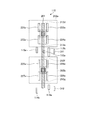
- FIG. 5 is a plan view showing an example of a first planar structure of a semiconductor substrate of one pixel sharing unit and a first wiring layer in the solid-state image sensor according to the first embodiment of the present disclosure.
- FIG. 5 is a plan view showing an example of a first planar structure on the first surface side of the semiconductor substrate of FIG.
- FIG. 5 is a plan view showing an example of a first planar structure of a first wiring layer of a plurality of pixel sharing units in the solid-state image sensor according to the first embodiment of the present disclosure.
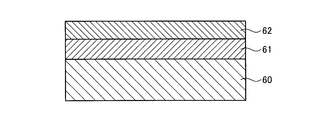
- 6 is a cross-sectional view showing a method of manufacturing a first wiring layer according to the first embodiment of the present disclosure in the cross section AA'of FIG. 6A (No. 1).
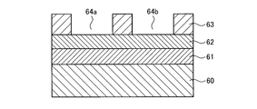
- 6 is a cross-sectional view showing a method of manufacturing the first wiring layer according to the first embodiment of the present disclosure in the cross section AA'of FIG. 6A (No. 2).
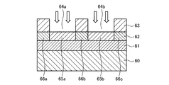
- 6 is a cross-sectional view showing a method of manufacturing a first wiring layer according to the first embodiment of the present disclosure in the cross section AA'of FIG. 6A (No. 3).
- It is sectional drawing which shows the manufacturing method of the 1st wiring layer which concerns on 1st Embodiment of this disclosure in the cross section of AA' of FIG. 6A (the 4).
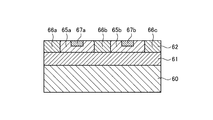
- 6 is a cross-sectional view showing a method of manufacturing a first wiring layer according to the first embodiment of the present disclosure in the cross section AA'of FIG. 6A (No. 5).
- FIG. 5 is a plan view showing an example of a first planar structure of a second wiring layer of a plurality of pixel sharing units in the solid-state image sensor according to the first embodiment of the present disclosure. It is sectional drawing which shows the manufacturing method of the 2nd wiring layer which concerns on 1st Embodiment of this disclosure in the BB'cross section of FIG. 7A (the 1). It is sectional drawing which shows the manufacturing method of the 2nd wiring layer which concerns on 1st Embodiment of this disclosure in the BB'cross section of FIG. 7A (the 2). It is sectional drawing which shows the manufacturing method of the 2nd wiring layer which concerns on 1st Embodiment of this disclosure in the BB'cross section of FIG. 7A (the 3).
- FIG. 1 It is a top view which shows the 2nd plane structure example of the 1st surface side of the semiconductor substrate of one pixel sharing unit in the solid-state image sensor which concerns on 1st Embodiment of this disclosure. It is a top view which shows the 2nd planar structure example of the 1st wiring layer of one pixel sharing unit in the solid-state image sensor which concerns on 1st Embodiment of this disclosure. It is a top view which shows the example of the 2nd planar structure of the 2nd wiring layer laminated on the 1st wiring layer of one pixel sharing unit in the solid-state image pickup apparatus which concerns on 1st Embodiment of this disclosure.
- FIG. 5 is a plan view showing another example of a second planar structure example of a second wiring layer laminated on a first wiring layer of one pixel sharing unit in the solid-state image sensor according to the first embodiment of the present disclosure. .. It is a top view which shows the plan structure example of the 1st wiring layer of a plurality of pixel sharing units in the solid-state image sensor which concerns on 2nd Embodiment of this disclosure.
- 11 is a cross-sectional view showing a method of manufacturing the first wiring layer according to the second embodiment of the present disclosure in the CC'cross section of FIG. 11A (No. 1).
- 11 is a cross-sectional view showing a method of manufacturing a first wiring layer according to a second embodiment of the present disclosure in the CC'cross section of FIG.
- FIG. 3 is a cross-sectional view showing a method of manufacturing a first wiring layer according to a second embodiment of the present disclosure in the CC'cross section of FIG. 11A (No. 3). It is sectional drawing which shows the manufacturing method of the 1st wiring layer which concerns on 2nd Embodiment of this disclosure in the CC'cross section of FIG. 11A (the 4).
- FIG. 5 is a cross-sectional view showing a method of manufacturing a first wiring layer according to a second embodiment of the present disclosure in the CC'cross section of FIG. 11A (No. 5).
- FIG. 13A shows the manufacturing method of the 1st wiring layer which concerns on 4th Embodiment of this disclosure in the DD'cross section of FIG. 13A (the 1). It is sectional drawing which shows the manufacturing method of the 1st wiring layer which concerns on 4th Embodiment of this disclosure in the DD'cross section of FIG. 13A (the 2).
- FIG. 13A shows the manufacturing method of the 1st wiring layer which concerns on 4th Embodiment of this disclosure in the DD'cross section of FIG. 13A (the 2).
- FIG. 3 is a cross-sectional view showing a method of manufacturing a first wiring layer according to a fourth embodiment of the present disclosure in the DD'cross section of FIG. 13A (No. 3). It is sectional drawing which shows the manufacturing method of the 1st wiring layer which concerns on the modification of 4th Embodiment of this disclosure. It is sectional drawing which shows the manufacturing method of the semiconductor device which concerns on 5th Embodiment of this disclosure (the 1). It is sectional drawing which shows the manufacturing method of the semiconductor device which concerns on 5th Embodiment of this disclosure (the 2). It is a block diagram which shows the schematic structure example of the semiconductor device which concerns on 6th Embodiment of this disclosure.
- First Embodiment 1.1 Configuration example of solid-state imaging device 1.2 Configuration example of unit pixel 1.3 Basic function example of unit pixel 1.4 Cross-sectional structure example of unit pixel 1.5 Semiconductor substrate and first wiring layer 1.6 Example of manufacturing method of semiconductor substrate and first wiring layer 1.7 Manufacturing method of semiconductor substrate and second wiring layer 1.8 Outline of manufacturing method of wiring layer 1.9 Insulation of wiring layer Structural changes in the film 1.10 Example of the second planar structure of the semiconductor substrate and the first wiring layer 1.11 Summary 2. Second embodiment 3. Third embodiment 4. Fourth embodiment 5. Fifth embodiment 6. Sixth Embodiment 7. Seventh Embodiment 8. Eighth embodiment 9. Ninth embodiment 10. Examples of application to electronic devices 11. Application example to endoscopic surgery system 12. Application example to mobile
- a solid-state image sensor and a method for manufacturing the solid-state image sensor which can achieve a partial increase / decrease in the wiring capacity by a simpler manufacturing process, will be described in detail with an example.
- FIG. 1 is a block diagram showing a schematic configuration example of a CMOS (Complementary Metal Oxide Semiconductor) type solid-state image sensor (hereinafter, simply referred to as a CMOS image sensor) according to the first embodiment.
- CMOS image sensor is an image sensor created by applying or partially using a CMOS process.
- the CMOS image sensor 10 according to the present embodiment is composed of a back-illuminated CMOS image sensor.
- the CMOS image sensor 10 has, for example, a stack structure in which a semiconductor chip on which a pixel array portion 11 is formed and a semiconductor chip on which peripheral circuits are formed are laminated.
- Peripheral circuits may include, for example, a vertical drive circuit 12, a column processing circuit 13, a horizontal drive circuit 14, and a system control unit 15.
- the CMOS image sensor 10 further includes a signal processing unit 18 and a data storage unit 19.
- the signal processing unit 18 and the data storage unit 19 may be provided on the same semiconductor chip as the peripheral circuit, or may be provided on another semiconductor chip.
- unit pixels (hereinafter, may be simply referred to as “pixels”) 50 having a photoelectric conversion element that generates and accumulates electric charges according to the amount of received light are arranged in the row direction and the column direction, that is, , It has a structure arranged in a matrix (also referred to as a two-dimensional lattice).
- the row direction means the arrangement direction of the pixels in the pixel row (in the drawing, the horizontal direction)
- the column direction means the arrangement direction of the pixels in the pixel row (in the drawing, the vertical direction).
- the pixel drive line LD is wired along the row direction for each pixel row and the vertical signal line VSL is wired along the column direction for each pixel row in the matrix-like pixel array.
- the pixel drive line LD transmits a drive signal for driving when reading a signal from the pixel.
- the pixel drive lines LD are shown as wiring one by one, but the wiring is not limited to one by one.
- One end of the pixel drive line LD is connected to the output end corresponding to each line of the vertical drive circuit 12.
- the vertical drive circuit 12 is composed of a shift register, an address decoder, and the like, and drives each pixel of the pixel array unit 11 simultaneously for all pixels or in units of rows. That is, the vertical drive circuit 12 constitutes a drive unit that controls the operation of each pixel of the pixel array unit 11 together with the system control unit 15 that controls the vertical drive circuit 12. Although the specific configuration of the vertical drive circuit 12 is not shown, it generally includes two scanning systems, a read scanning system and a sweep scanning system.
- the read-out scanning system selectively scans the unit pixels of the pixel array unit 11 row by row in order to read a signal from the unit pixels.
- the signal read from the unit pixel is an analog signal.
- the sweep-out scanning system performs sweep-out scanning for the read-out row on which read-out scanning is performed by the read-out scanning system, ahead of the read-out scan by the exposure time.
- the photoelectric conversion element is reset by sweeping out unnecessary charges from the photoelectric conversion element of the unit pixel of the read line. Then, the so-called electronic shutter operation is performed by sweeping (resetting) unnecessary charges with this sweep scanning system.
- the electronic shutter operation refers to an operation of discarding the electric charge of the photoelectric conversion element and starting a new exposure (starting the accumulation of electric charge).
- the signal read by the read operation by the read scanning system corresponds to the amount of light received after the read operation or the electronic shutter operation immediately before that. Then, the period from the read timing by the immediately preceding read operation or the sweep timing by the electronic shutter operation to the read timing by the current read operation is the charge accumulation period (also referred to as the exposure period) in the unit pixel.
- the signal output from each unit pixel of the pixel row selectively scanned by the vertical drive circuit 12 is input to the column processing circuit 13 through each of the vertical signal lines VSL for each pixel column.
- the column processing circuit 13 performs predetermined signal processing on the signal output from each pixel in the selected row through the vertical signal line VSL for each pixel column of the pixel array unit 11, and temporarily processes the pixel signal after the signal processing. Hold on.
- the column processing circuit 13 performs at least noise removal processing, for example, CDS (Correlated Double Sampling) processing and DDS (Double Data Sampling) processing as signal processing.
- CDS Correlated Double Sampling
- DDS Double Data Sampling
- the CDS process removes pixel-specific fixed pattern noise such as reset noise and threshold variation of the amplification transistor in the pixel.
- the column processing circuit 13 also has, for example, an AD (analog-digital) conversion function, and converts an analog pixel signal read from a photoelectric conversion element into a digital signal and outputs the signal.
- AD analog-digital
- the horizontal drive circuit 14 is composed of a shift register, an address decoder, and the like, and reads out circuits (hereinafter referred to as pixel circuits) corresponding to the pixel strings of the column processing circuit 13 are sequentially selected.
- pixel circuits reads out circuits
- the system control unit 15 is composed of a timing generator or the like that generates various timing signals, and based on the various timings generated by the timing generator, the vertical drive circuit 12, the column processing circuit 13, the horizontal drive circuit 14, and the like Drive control is performed.
- the signal processing unit 18 has at least an arithmetic processing function, and performs various signal processing such as arithmetic processing on the pixel signal output from the column processing circuit 13.
- the data storage unit 19 temporarily stores data necessary for the signal processing in the signal processing unit 18.
- the image data output from the signal processing unit 18 may be, for example, executed by a processor or the like in an electronic device equipped with a CMOS image sensor 10 described later, or transmitted to the outside via a predetermined network. You may.
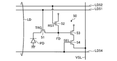
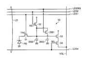
- FIG. 2 is a circuit diagram showing a schematic configuration example of a unit pixel according to the first embodiment.
- the unit pixel 50 includes a photodiode PD, a transfer transistor (also referred to as a transfer gate) 51, a reset transistor (also referred to as a reset gate) 52, and an amplification transistor (also referred to as an amplification gate) 53. It includes a selection transistor (also referred to as a selection gate) 54 and a floating diffusion layer FD.
- the transfer transistor 51, the reset transistor 52, the amplification transistor 53, and the selection transistor 54 are also referred to as pixel transistors, respectively.
- the selection transistor drive line LD54 included in the pixel drive line LD is connected to the gate of the selection transistor 54, and the reset transistor drive line LD 52 included in the pixel drive line LD is connected to the gate of the reset transistor 52.
- the transfer transistor drive line LD51 included in the pixel drive line LD is connected to the gate of 51.
- a vertical signal line VSL having one end connected to the column processing circuit 13 is connected to the drain of the amplification transistor 53 via the selection transistor 54.
- the reset transistor 52, the amplification transistor 53, and the selection transistor 54 are also collectively referred to as a pixel circuit.
- the pixel circuit may include a floating diffusion layer FD and / or a transfer transistor 51. Further, a pixel circuit that does not include the selection transistor 54 may be used.
- the photodiode PD photoelectrically converts the incident light.
- the transfer transistor 51 transfers the electric charge generated in the photodiode PD.
- the floating diffusion layer FD accumulates the electric charge transferred by the transfer transistor 51.
- the amplification transistor 53 causes a pixel signal having a voltage value corresponding to the electric charge accumulated in the floating diffusion layer FD to appear on the vertical signal line VSL.
- the reset transistor 52 releases the electric charge accumulated in the floating diffusion layer FD.
- the selection transistor 54 selects the unit pixel 50 to be read.
- the anode of the photodiode PD is grounded, and the cascade is connected to the source of the transfer transistor 51.
- the drain of the transfer transistor 51 is connected to the source of the reset transistor 52 and the gate of the amplification transistor 53, and the nodes at these connection points form the floating diffusion layer FD.
- the drain of the reset transistor 52 is connected to a vertical reset input line (not shown).
- the source of the amplification transistor 53 is connected to a vertical current supply line (not shown).
- the drain of the amplification transistor 53 is connected to the source of the selection transistor 54, and the drain of the selection transistor 54 is connected to the vertical signal line VSL.
- the floating diffusion layer FD converts the accumulated electric charge into a voltage having a voltage value corresponding to the amount of the electric charge.
- the floating diffusion layer FD may have, for example, a grounding capacitance.
- the present invention is not limited to this, and the floating diffusion layer FD is added by intentionally connecting a capacitor or the like to a node to which the drain of the transfer transistor 51, the source of the reset transistor 52, and the gate of the amplification transistor 53 are connected. It may be a capacity.
- the reset transistor 52 controls the discharge (reset) of the electric charge stored in the floating diffusion layer FD according to the reset signal RST supplied from the vertical drive circuit 12 via the reset transistor drive line LD52.
- the transfer transistor 51 By turning on the transfer transistor 51 when the reset transistor 52 is in the ON state, in addition to the electric charge accumulated in the floating diffusion layer FD, the electric charge accumulated in the photodiode PD is discharged (reset). It is also possible to do.
- the floating diffusion layer FD is electrically disconnected from the vertical reset input line and becomes a floating state.
- the photodiode PD photoelectrically converts the incident light and generates an electric charge according to the amount of the light.
- the generated charge is accumulated on the cathode side of the photodiode PD.
- the transfer transistor 51 controls the transfer of electric charges from the photodiode PD to the floating diffusion layer FD according to the transfer control signal TRG supplied from the vertical drive circuit 12 via the transfer transistor drive line LD51.
- the floating diffusion layer FD has a function of converting the electric charge transferred from the photodiode PD via the transfer transistor 51 into a voltage having a voltage value corresponding to the amount of the electric charge. Therefore, in the floating state in which the reset transistor 52 is turned off, the potential of the floating diffusion layer FD is modulated according to the amount of electric charge accumulated by each.
- the amplification transistor 53 functions as an amplifier that uses the potential fluctuation of the floating diffusion layer FD connected to the gate as an input signal, and the output voltage signal appears as a pixel signal on the vertical signal line VSL via the selection transistor 54.
- the selection transistor 54 controls the appearance of the pixel signal by the amplification transistor 53 on the vertical signal line VSL according to the selection control signal SEL supplied from the vertical drive circuit 12 via the selection transistor drive line LD54. For example, when a high level selection control signal SEL is input to the gate of the selection transistor 54, the pixel signal by the amplification transistor 53 appears on the vertical signal line VSL. On the other hand, when the Low level selection control signal SEL is input to the gate of the selection transistor 54, the appearance of the pixel signal on the vertical signal line VSL is stopped. As a result, in the vertical signal line VSL in which a plurality of unit pixels 50 are connected, it is possible to take out only the output of the selected unit pixel 50.
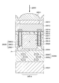
- FIG. 3 is a cross-sectional view showing an example of a cross-sectional structure of the solid-state image sensor according to the present embodiment.
- the photodiode 20001 (corresponding to the above-mentioned photodiode PD) receives the incident light 20001 incident from the back surface (upper surface in the figure) side of the semiconductor substrate 20018.
- a flattening film 20013, a CF (color filter) 20012, and a microlens 20011 are provided above the photodiode 20001.
- the incident light 20001 incident through each part is received by the light receiving surface 200017 and converted to photoelectric light. Is done.
- the n-type semiconductor region 20020 is formed as a charge storage region for accumulating charges (electrons).
- the n-type semiconductor region 20020 is provided inside the p-type semiconductor regions 2016, 20044 of the semiconductor substrate 20018.
- a p-type semiconductor region 20044 having a higher impurity concentration than the back surface (upper surface) side is provided.
- the photodiode 20001 has a HAD (Hole-Accumulation Diode) structure, and p is suppressed so as to suppress the generation of dark current at each interface between the upper surface side and the lower surface side of the n-type semiconductor region 20020.
- the type semiconductor regions 2016 and 20044 are formed.
- a pixel separation unit 20030 that electrically separates a plurality of pixels 20010 (corresponding to the above-mentioned unit pixel 50) is provided, and in the region partitioned by the pixel separation unit 20030. , Photodiode 20001 is provided.
- the pixel separation unit 20030 is formed in a grid pattern so as to intervene between a plurality of pixels 20010, for example, and the photodiode 20001 has the pixel separation. It is formed in the area partitioned by the part 20030.
- each photodiode 20001 the anode is grounded, and in the solid-state imaging device, the signal charge (for example, electrons) accumulated in the photodiode 20019 is transmitted via a transfer transistor (MOSFET (Field-Effect Transistor)) or the like (not shown). Is read out and output as an electric signal to a vertical signal line VSL (not shown).
- MOSFET Field-Effect Transistor
- the wiring layer 20050 is provided on the front surface (lower surface) of the semiconductor substrate 20018 opposite to the back surface (upper surface) where the light-shielding film 2014, CF2012, microlens 20011 and the like are provided.
- the wiring layer 20050 includes the wiring 20051 and the insulating layer 20052, and is formed so that the wiring 20051 is electrically connected to each element in the insulating layer 20052.
- the wiring layer 20050 is a layer of so-called multi-layer wiring, and is formed by alternately laminating the interlayer insulating film constituting the insulating layer 20052 and the wiring 20051 a plurality of times.
- wiring to a transistor for reading charge from a photodiode 20001 such as a transfer transistor and wiring such as a vertical signal line VSL are laminated via an insulating layer 20052.
- a support substrate 20061 is provided on the surface of the wiring layer 20050 opposite to the side on which the photodiode 20019 is provided.
- a substrate made of a silicon semiconductor having a thickness of several hundred ⁇ m is provided as a support substrate 20061.
- the light-shielding film 2014 is provided on the back surface side (upper surface in the figure) of the semiconductor substrate 20018.
- the light-shielding film 2014 is configured to block a part of the incident light 20001 directed from above the semiconductor substrate 20018 toward the back surface of the semiconductor substrate 20018.
- the light-shielding film 2014 is provided above the pixel separation portion 20030 provided inside the semiconductor substrate 20018.
- the light-shielding film 2014 is provided on the back surface (upper surface) of the semiconductor substrate 20018 so as to project in a convex shape via an insulating film 2015 such as a silicon oxide film.
- the light-shielding film 20144 is not provided and is open so that the incident light 20001 is incident on the photodiode 20001. ..
- the planar shape of the light-shielding film 2014 is a grid pattern, and an opening through which the incident light 20001 passes to the light receiving surface 200017 is formed.
- the light-shielding film 2014 is formed of a light-shielding material that blocks light.
- the light-shielding film 2014 is formed by sequentially laminating a titanium (Ti) film and a tungsten (W) film.
- the light-shielding film 2014 can be formed, for example, by sequentially laminating a titanium nitride (TiN) film and a tungsten (W) film.
- the light-shielding film 2014 is covered with a flattening film 2013.
- the flattening film 2013 is formed by using an insulating material that transmits light.
- the pixel separation unit 20030 has a groove portion 20031, a fixed charge film 20032, and an insulating film 20033.
- the fixed charge film 20032 is formed on the back surface (upper surface) side of the semiconductor substrate 20018 so as to cover the groove portion 20031 partitioning between the plurality of pixels 20010.
- the fixed charge film 20032 is provided so as to cover the inner surface of the groove portion 20033 formed on the back surface (upper surface) side of the semiconductor substrate 20018 with a constant thickness. Then, an insulating film 20033 is provided (filled) so as to embed the inside of the groove portion 20033 covered with the fixed charge film 20032.
- the fixed charge film 20032 uses a high dielectric having a negative fixed charge so that a positive charge (hole) storage region is formed at the interface with the semiconductor substrate 20018 and the generation of dark current is suppressed. Is formed. Since the fixed charge film 20032 is formed so as to have a negative fixed charge, an electric field is applied to the interface with the semiconductor substrate 20018 by the negative fixed charge, and a positive charge (hole) storage region is formed.
- the fixed charge film 20032 can be formed of, for example, a hafnium oxide film (HfO 2 film).
- the fixed charge film 20032 can be formed so as to contain at least one of other oxides such as hafnium, zirconium, aluminum, tantalum, titanium, magnesium, yttrium, and lanthanoid elements.
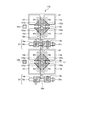
- FIG. 4 is a plan view showing an example of a first planar structure of a semiconductor substrate of one pixel sharing unit and a first wiring layer according to the first embodiment. Note that FIG. 4 shows an example of a first planar structure in the pixel sharing unit 110. The details of each layer shown in FIG. 4 will be described later with reference to FIGS. 5A to 5C.
- the sharing pattern shown in FIG. 4 is an example. Therefore, the configuration is not limited to the configuration illustrated in FIG. 4, and there are various structures such as a structure in which two photodiode PDs share one floating diffusion layer FD, and a structure in which four photodiode PDs share one amplification transistor 53.
- This embodiment can also be applied to a pixel sharing pattern. Further, the present embodiment can be applied to a structure that does not form a pixel sharing unit, for example, a structure in which the unit pixel configurations of FIG. 2 are arranged independently.
- FIG. 5A is a plan view showing an example of a first planar structure on the first surface side of the semiconductor substrate of FIG. 4, in which the semiconductor substrate 20018 on which the light receiving portion is formed in the solid-state imaging device as shown in FIG. 3 and , Is a plan view of the insulating layer 20052 on which the gate electrode of the pixel transistor shown in FIG. 2 is formed.
- the first surface may be an element forming surface of the semiconductor substrate 20018.
- the pixel sharing unit 110 is composed of a first light receiving unit 21, a second light receiving unit 22, a first transistor group 31, and a second transistor group 32. Further, the pixel sharing unit 110 has a first well contact 23a corresponding to the first light receiving unit 21 and a second well contact 23b corresponding to the second light receiving unit 22.
- the first well contact 23a and the second well contact 23b function as contacts for fixing the potentials of the first light receiving unit 21 and the second light receiving unit 22 on the semiconductor substrate 20018 to the ground potential or an arbitrary potential, respectively.
- a plurality of well contacts may not necessarily be provided. For example, it is possible to form one well contact with a plurality of light receiving units or a semiconductor substrate 20018.
- the first light receiving unit 21 is composed of four photodiodes 111 to 114, a floating diffusion layer 16a shared by them, and transfer gates 121a to 124a connecting the photodiodes 111 to 114, respectively.
- the second light receiving unit 22 is composed of four photodiodes 115 to 118, a floating diffusion layer 16b shared by them, and transfer gates 125a to 128a connecting the photodiodes 115 to 118, respectively.
- the first transistor group 31 is composed of an amplification gate 13a, a selection gate 15a, and source / drain (S / D) 31a to 31c.
- the second transistor group 32 is composed of a first reset gate 14a, a second reset gate 14b, and source / drain (S / D) 32a to 32c.
- the configuration is such that two reset gates are provided in FIG. 5A, since even one reset gate can be operated, a configuration in which the second reset gate 14b is not provided is also possible. Further, even when the second reset gate 14b is not operated as a dummy, the layout symmetry with the first transistor group 31 can be provided by providing the second reset gate 14b. As a result, it is possible to suppress variations in characteristics between pixels.
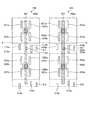
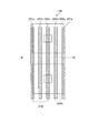
- FIG. 5B is a plan view showing an example of a first planar structure of the first wiring layer of FIG. 4, and is the most semiconductor substrate among the wiring 20051 included in the wiring layer 20050 in the solid-state image sensor as shown in FIG. It is a top view of the 1st wiring layer provided on the 20018 side.
- the region 202a corresponds to the first light receiving portion 21 in FIG. 5A in the substrate thickness direction of the semiconductor substrate 20018, and the region 202b corresponds to the second light receiving portion 22 in FIG. 5A in the same direction.
- the first wiring layer has an FD wiring 201 connecting the floating diffusion layers 16a and 16b as shown in FIG. 5A, for example.
- the FD wiring 201 can also be replaced with an FD wiring that connects the floating diffusion layers 16a and 16b and the amplification gate 13a.
- the FD wiring 201 may be an FD wiring having these two functions.
- the wiring provided in the first wiring layer for example, there are transfer gate wirings 221a to 228a for operating the transfer gates 121a to 128a. Further, the amplification gate wiring 113a for operating the pixel transistor, the first reset gate wiring 114a, the second reset gate wiring 114b, such as the amplification gate 13a, the first reset gate 14a, the second reset gate 14b, and the selection gate 15a, are selected.
- the gate wiring 115a can also be provided in the first wiring layer.
- source / drain wirings 113b, 311 and 312 connected to the source / drain (S / D) in the first transistor group 31 and the second transistor group 32 can be provided in the first wiring layer.
- some of the above-mentioned wirings may be provided in another wiring layer, or wirings having other functions may be provided in the first wiring layer. Further, the wiring may be shared as appropriate, or a separate system may be used.
- FIG. 5C is a plan view showing an example of a first planar structure of the second wiring layer laminated on the first wiring layer of FIG. 4, and is included in the wiring layer 20050 in the solid-state imaging device as shown in FIG. It is a top view of the 2nd wiring layer provided on the semiconductor substrate 20018 side next to the 1st wiring layer shown in FIG. 5B in the wiring 20051.
- the region 203a corresponds to the first light receiving portion 21 in FIG. 5A and the region 202a in FIG. 5B in the substrate thickness direction of the semiconductor substrate 20018, and the region 203b corresponds to the second light receiving portion 22 and the second light receiving portion 22 in FIG. 5A in the same direction.
- the second wiring layer has wirings 211a to 211c used as wiring capacitance, for example.
- the wiring capacity of the FD wiring 201 is increased, and more charges generated by the photodiodes 111 to 118 can be stored.
- the amount of charge accumulation can be increased by using the wiring capacitance as shown in FIG. 5C. This can contribute to the expansion of the dynamic range, that is, the increase in the number of saturated accumulated charges.
- the second wiring layer may have a configuration in which at least a part of the wirings 211a to 211c is connected to at least a part of the transfer gate wirings 221a to 228a shown in FIG. 5B, for example.
- an additional capacity can be added between the transfer gates 121a to 128a and the FD wiring 201, and the wiring capacity between them can be increased.
- the wiring capacitance for example, the coupling action between the transfer gates 121a to 128a and the FD wiring 201 becomes large, and when the potential of the transfer gates 121a to 128a rises, the potential of the floating diffusion layer FD also becomes high and the electric charge is increased. Is easier to read. As a result, reading defects can be reduced.
- the second wiring layer is not limited to the configuration that forms the wiring capacity.
- wiring having different functions such as a vertical signal line VSL for transmitting a pixel signal and a wiring for transmitting a transistor drive signal may be formed in the second wiring layer.
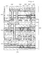
- FIG. 6A is a plan view showing an example of a first plan structure of a first wiring layer of a plurality of pixel sharing units according to the first embodiment.
- the pixel sharing unit 110 shown in FIG. 5A and the pixel sharing unit 110 are arranged adjacent to the pixel sharing unit 110 in a direction horizontal to the first surface of the semiconductor substrate 20018 on which the pixel sharing unit 110 is formed. It is a top view with a pixel sharing unit 310.
- the pixel sharing unit 310 has the same configuration as the pixel sharing unit 110. Specifically, as shown in FIG. 6A, the pixel sharing unit 310 includes the FD wiring 401, the transfer gate wirings 421a to 428a, the amplification gate wiring 413a, the first reset gate wiring 414a, and the second reset gate wiring.
- the first wiring layer includes 414b, selective gate wiring 415a, transistor source / drain wirings 411, 421, 413b, and regions 402a and 402b.
- the pixel sharing unit 310 a plan view of the semiconductor substrate 20018 on which the light receiving portion is formed and the insulating layer 20052 on which the gate electrode of the pixel transistor shown in FIG. 2 is formed is not shown, but the pixels shown in FIG. 5A are shown. It may be the same as the configuration of the shared unit 110.
- the pixel sharing unit 310 is composed of a third light receiving unit, a fourth light receiving unit, a third transistor group, and a fourth transistor group.
- the region 402a is a third light receiving portion (not shown) provided on the semiconductor substrate 20018 adjacent to the first light receiving portion 21 in a direction horizontal to the first surface of the semiconductor substrate 20018 in the substrate thickness direction of the semiconductor substrate 20018.
- the region 402b corresponds to a fourth light receiving portion (not shown) provided on the semiconductor substrate 20018 adjacent to the second light receiving portion 22 in the same horizontal direction in the substrate thickness direction.
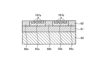
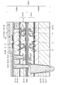
- FIGS. 6B to 6F are cross-sectional views showing a method of manufacturing the first wiring layer according to the first embodiment in the cross section AA'shown in FIG. 6A.
- examples of each manufacturing process will be described with reference to FIGS. 6B to 6F.
- the process of forming an insulating film on the semiconductor substrate is shown. This is, for example, a step of forming the semiconductor substrate 20018 of FIG. 3 and the insulating layer 200025 of the wiring layer 20050. Specifically, as shown in FIG. 6B, the protective insulating film 61 and the interlayer insulating film 62 are formed on the semiconductor substrate 60 on which the element is formed.
- the protective insulating film 61 for example, an insulating film material such as a silicon oxide film (SiO 2 ) or a silicon nitride film (SiN) can be used. Further, for forming the protective insulating film 61, for example, a general film forming technique such as CVD (Chemical Vapor Deposition) or sputtering can be used.
- CVD Chemical Vapor Deposition
- insulating film materials can also be used for the protective insulating film 61.
- Other insulating film materials include, for example, a silicon nitride film (SiN) and a silicon oxynitride film (SiON).
- the protective insulating film 61 can function as, for example, a protective film of the interlayer insulating film 62 in the process process or an etching stopper. Further, by providing the protective insulating film 61, it is possible to improve the mechanical strength of the interlayer insulating film 62, the wiring layer 20050, and the solid-state image sensor 10.
- the adhesive strength of the interlayer insulating film 62 to the semiconductor substrate 60 can be improved, and the transistors formed on the semiconductor substrate 60 can be improved. It is possible to improve the operational stability of the circuit element of.
- the interlayer insulating film 62 a film material having a lower dielectric constant than that of the silicon oxide film (SiO 2 ), such as a carbon-added silicon oxide film (SiOC) or a SiCOH film, can be used.
- SiO 2 silicon oxide film
- SiOC carbon-added silicon oxide film
- SiCOH film SiCOH film
- the interlayer insulating film 62 not only the above-mentioned mixed material of an organic material and an inorganic material but also other inorganic materials and organic materials can be used as the low dielectric constant film material.
- the inorganic material include fluoridated silicon oxide film (SiOF) and hydrogenated silsesquioxane (HSQ).
- the organic material include a parerin type and a polyallyl ether type.
- the mixed material of the organic material and the inorganic material other than the carbon-added silicon oxide film (SiOC) and the SiCOH film include methylated silsesquioxane (MSQ).
- the low dielectric constant film can also be formed by introducing pores into the insulating film material and using a material that is made porous. Specifically, the dielectric constant of the insulating film can be lowered by reducing the density of the film by, for example, heat or drying.
- the permittivity ⁇ is an index showing the degree of dielectric polarization of a substance.
- the value obtained by dividing the permittivity ⁇ of a substance by the permittivity ⁇ 0 of a vacuum is called the relative permittivity ⁇ r .
- the low dielectric constant in the present disclosure indicates that the relative permittivity is low.
- the relative permittivity may be simply referred to as the permittivity.
- the capacitance between wirings can be reduced. As a result, the capacitance between wirings is reduced, and high-speed operation of semiconductor elements, high-speed signal transmission, and reduction of power consumption become possible.
- FIG. 6B shows a configuration in which the protective insulating film 61 is provided
- the interlayer insulating film 62 may be directly formed on the semiconductor substrate 60.
- an insulating film such as a silicon oxide film (SiO 2 ) which is not a low dielectric constant film on the interlayer insulating film 62.
- SiO 2 silicon oxide film
- the insulating film may be laminated in one layer or in multiple layers.
- the first insulating film can be formed on the semiconductor substrate 60.
- the first insulating film may be a protective insulating film 61 or an interlayer insulating film 62.
- the configuration in which the protective insulating film 61 and the interlayer insulating film 62 are provided is shown, but the present invention is not limited to the insulating films having their respective functions.
- a first insulating film having a function different from that of the protective insulating film 61 instead of the protective insulating film 61 and / or the interlayer insulating film 62 is formed on the semiconductor substrate 60 on which the element is formed.
- a configuration in which the 61 and / or a second insulating film 62 different from the interlayer insulating film 62 is formed is also possible.
- the hierarchical relationship between the first insulating film 61 and the second insulating film 62 on the semiconductor substrate 60 may be interchanged. That is, the first insulating film 61 may be arranged on the semiconductor substrate 60, the second insulating film 62 may be arranged on the first insulating film 61, or the second insulating film 62 may be arranged on the semiconductor substrate 60. 62 is arranged, and the first insulating film 61 may be arranged on the second insulating film 62.
- the stacking order of the protective insulating film 61 and the interlayer insulating film 62 laminated on the semiconductor substrate 60 on which the element is formed may be the order of the interlayer insulating film 62 and the protective insulating film 61.
- a plurality of layers of the protective insulating film 61 and the interlayer insulating film 62 can be provided. It is also possible to repeatedly provide a laminated pattern of the protective insulating film 61 and the interlayer insulating film 62.
- a mask 63 having desired openings 64a and 64b is formed above the interlayer insulating film 62.
- a resist mask or a hard mask can be used for the mask 63.
- the process of changing the relative permittivity of the insulating film from the opening is shown. Specifically, as shown in FIG. 6D, the exposed regions 65a and 65b of the interlayer insulating film 62 exposed from the openings 64a and 64b are changed. For example, the state of the exposed regions 65a and 65b is changed by performing ion implantation or ashing from the openings 64a and 64b. Thereby, the relative permittivity of the exposed regions 65a and 65b of the interlayer insulating film 62 can be changed with respect to the relative permittivity of the shielding regions 66a, 66b and 66c covered with the mask 63.
- a specific method for changing the state of the exposed areas 65a and 65b will be described.
- ion implantation for example, there is a method of locally implanting ions of atoms such as argon (Ar), krypton (Kr), and xenon that are difficult to bond with silicon (Si) atoms into the exposed regions 65a and 65b.
- the exposed regions 65a and 65b may be changed in state by injecting silicon (Si) atoms, which have a small effect even if they remain in the interlayer insulating film 62.
- it is also possible to control the change given to the exposed regions 65a and 65b by controlling the amount of energy and the amount of dose of ion implantation. It is also possible to control the changes given to the exposed regions 65a and 65b by selecting the ions to be ion-implanted.
- ashing for example, photoexcited ashing that irradiates ultraviolet rays to promote the chemical reaction between the gas and the exposed regions 65a and 65b, and plasma that turns the gas into plasma and uses it to change the exposed regions 65a and 65b.
- ashing for example, photoexcited ashing that irradiates ultraviolet rays to promote the chemical reaction between the gas and the exposed regions 65a and 65b, and plasma that turns the gas into plasma and uses it to change the exposed regions 65a and 65b.
- methods such as ashing.
- the relative permittivity of the exposed regions 65a and 65b can be changed with respect to the relative permittivity of the shielded regions 66a, 66b and 66c covered with the mask 63.
- the relative permittivity of the exposed regions 65a and 65b can be made higher than the relative permittivity of the shielding regions 66a, 66b and 66c.
- the regions 202a and 402a in FIG. 6A correspond to the exposed regions 65a and 65b, respectively.
- the interlayer insulating film 62 in the vicinity of the FD wirings 201 and 401 can have a high dielectric constant.
- the wiring capacity of the regions 202a and 402a can be partially increased.
- the film densities of the exposed regions 65a and 65b may be higher than those of the shielding regions 66a, 66b and 66c.
- the surface of the exposed regions 65a and 65b or the pores of a part or the whole of the exposed regions 65a and 65b are reduced.
- the film density of a part or all of the exposed regions 65a and 65b surfaces or the exposed regions 65a and 65b is increased, and the dielectric constant is increased.
- the wiring capacity of the regions 202a and 402a can be partially increased. Specifically, the wiring capacity of the FD wirings 201 and 401 can be increased.
- the film thickness of the exposed regions 65a and 65b may be thinner than the film thickness of the shielding regions 66a, 66b and 66c.
- the pores in a part or the whole of the exposed regions 65a and 65b or the surface thereof are reduced, and the film density is increased.
- the exposed regions 65a and 65b are in a compressed state, and as a result, the film thickness of the exposed regions 65a and 65b becomes thinner than the film thickness of the shielding regions 66a, 66b and 66c.
- the process of removing the mask on the insulating film is shown. Specifically, as shown in FIG. 6E, the mask 63 is peeled off. After that, in order to stabilize the surface of the interlayer insulating film 62 on the side where the mask is formed, annealing may be performed arbitrarily.
- desired wirings 67a and 67b are formed on the interlayer insulating film 62.
- a conductive material is used for the wirings 67a and 67b.
- metal materials such as copper (Cu), tungsten (W), and aluminum (Al) can be used.
- Cu copper
- W tungsten
- Al aluminum
- a damascene process is used to open the region where the wirings 67a and 67b are formed, to form copper, and to flatten the surface of the wiring 67a. , 67b is formed.
- the wiring 67a is an example of the first wiring described in the claims
- the interlayer insulating film 62 is an example of the first insulating film
- the exposed region 65a is the first.
- the shielding region 66a is an example of a region
- the shielding region 66a is an example of a second region.
- the correspondence between each component described in the claims and each component described in the specification is not limited to the above, and the correspondence is appropriately as long as it does not deviate from the gist of the present disclosure. Can be applied to each embodiment or a modification thereof.
- FIG. 6F shows a process of forming wirings 67a and 67b in the exposed areas 65a and 65b, respectively.
- the FD wirings 201 and 401 in FIG. 6A correspond to the wirings 67a and 67b, respectively.
- the interlayer insulating film 62 (specifically, the exposed regions 65a and 65b) in the vicinity of the FD wirings 201 and 401, and the FD wirings 201 from the direction parallel to and perpendicular to the first surface.
- the region in contact with 401 can be partially increased in dielectric constant. Thereby, for example, the wiring capacity of the FD wirings 201 and 401 can be increased.
- the wiring capacitance formed in the exposed regions 65a and 65b of high dielectric constant in FIG. 6F is used.
- the amount of charge accumulation can be increased. This can contribute to the expansion of the dynamic range, that is, the increase in the number of saturated accumulated charges.
- the surface (second surface) on the semiconductor substrate 60 side in the exposed regions 65a and 65b is closer to the semiconductor substrate 60 than the surface (third surface) on the semiconductor substrate side in the wirings 67a and 67b.
- the wirings 67a and 67b are not limited to the FD wirings 201 and 401.
- the wirings 67a and 67b correspond to at least one of the transfer gate wirings 221a to 224a and 421a to 424a, and the wiring capacitance of at least a part of the transfer gate wirings 221a to 224a and 421a to 424a can be increased.
- FD wirings 201 and 401 and transfer gate wirings 221a to 224a and 421a to 424a are formed in the exposed areas 65a and 65b, and transfer gate wirings 221a to 224a and 421a to 424a and FD wirings 201 and 401 are formed.
- An additional capacity can be added between the and, and the wiring capacity during this period can be increased.
- the coupling action between the transfer gates (not shown) connected to the transfer gate wirings 221a to 224a and the FD wirings 201 and 401 increases, and the potential of the transfer gate increases.
- the potential of the floating diffusion layer FD also increases, making it easier to read the charge. As a result, reading defects can be reduced. Further, since the charge transfer from the photodiode PD to the floating diffusion layer FD is accelerated, the pixel signal for the unit pixel 50 can be read out at high speed.
- wiring may be formed in at least a part of the shielding areas 66a, 66b, 66c.
- another configuration example in which the exposed regions 65a and 65b do not correspond to the regions 202a and 402a of FIG. 6A may be included in the present embodiment.
- the FD wiring 201 is formed in the exposed area 65a
- the FD wiring 401 is formed in the exposed area 65b
- the transfer gate wirings 221a and 223a are formed in the shielding area 66a
- the transfer gate wirings 222a, 224a, 421a and 423a are formed in the shielding area 66b.
- the regions 202a and 402a of FIG. 6A correspond to the exposed regions 65a and 65b of FIGS. 6D to 6F, respectively, but the present invention is not limited to this.
- the exposed regions 65a and 65b do not have to be adjacent pixel sharing units like the regions 202a and 402a, and the exposed regions 65a and the shielding regions 66a may be formed in at least a part of the solid-state image sensor 10.
- the exposed regions 65a and 65b may correspond to the regions 202a, 202b, 402a and 402b of FIG. 6A in a direction parallel to the first surface of the semiconductor substrate 20018.
- the regions 202b and 402b can also change the state of the interlayer insulating film 62 as a part of the exposed regions 65a and 65b.
- the exposed regions 65a and 65b may correspond to, for example, the region 212a of FIG. 5B or FIG. 6A and the region 412a of FIG. 6A in the direction parallel to the first surface of the semiconductor substrate 20018.
- the state of the interlayer insulating film 62 in the vicinity of the FD wirings 201 and 401 formed in the first wiring layer can be changed in a wide range.
- the regions 202a, 202b, 402a, and 402b they are connected to the above-mentioned first transistor group 31, second transistor group 32, third transistor group (not shown), and fourth transistor group (not shown). Regions forming the wiring may also be included in the exposed regions 65a and 65b.
- a low dielectric constant film is used for the interlayer insulating film 62 and the dielectric constant of the exposed regions 65a and 65b to which the state is changed is increased as compared with the shielding regions 66a, 66b and 66c.
- the dielectric constant of the exposed regions 65a and 65b to which the state is changed may be further reduced as compared with the shielding regions 66a, 66b and 66c. Conceivable.
- the dielectric constants of the exposed regions 65a and 65b can be adjusted to the shielding regions 66a and 66a. It may be increased or decreased as compared with 66b and 66c.
- the FD wiring is formed in the region of low dielectric constant, the FD capacitance can be reduced. As a result, for example, the charge-voltage conversion efficiency (gain) in the amplification transistor 53 in which the charge held by the floating diffusion layer FD is input to the gate electrode is increased.
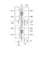
- FIG. 7A is a plan view showing an example of a first plan structure of a second wiring layer of a plurality of pixel sharing units according to the first embodiment.
- the pixel sharing unit 110 shown in FIG. 5A and the pixel sharing unit 110 are arranged adjacent to the pixel sharing unit 110 in a direction horizontal to the first surface of the semiconductor substrate 20018 on which the pixel sharing unit 110 is formed. It is a top view with a pixel sharing unit 310.
- the pixel sharing unit 310 may have the same configuration as the pixel sharing unit 110. Specifically, as shown in FIG. 7A, the pixel sharing unit 310 has wirings 211d to 211f in the second wiring layer.
- the wirings 211d to 211f are used, for example, as wiring capacitances, like the wirings 211a to 211c described above.
- an additional capacity for the FD wiring 401 can be formed.
- the transfer gate (not shown) of the pixel sharing unit 310 and the FD wiring 401 can be connected to each other.
- An additional capacity can be added between them to increase the wiring capacity during this period.
- the wirings 211a to 211f are not limited to the configuration that forms the wiring capacity.
- wiring having different functions such as a vertical signal line VSL for transmitting a pixel signal and a wiring for transmitting a transistor drive signal may be used.
- the region 403a includes a third light receiving portion (not shown) provided on the semiconductor substrate 20018 adjacent to the first light receiving portion 21 in a direction horizontal to the first surface of the semiconductor substrate 20018 in the substrate thickness direction of the semiconductor substrate 20018.
- the region 403b is a fourth light receiving portion (not shown) provided on the semiconductor substrate 20018 adjacent to the second light receiving portion 22 in the same horizontal direction in the substrate thickness direction and FIG. Corresponds to region 402b in 6A.
- the regions 203a and 403a of FIG. 7A correspond to the exposed regions 65a and 65b of FIGS. 7D to 7F, respectively, but the present invention is not limited to this.
- the exposed regions 65a and 65b do not have to be adjacent pixel sharing units like the regions 203a and 403a, and the exposed regions 65a and the shielding region 66a may be formed in at least a part of the solid-state image sensor 10.
- the exposed regions 65a and 65b may correspond to the regions 203a, 203b, 403a and 403b of FIG. 7A in a direction parallel to the first surface of the semiconductor substrate 20018.
- the regions 203b and 403b can also change the state of the interlayer insulating film 62 as a part of the exposed regions 65a and 65b.
- the exposed regions 65a and 65b may correspond to, for example, the region 212b of FIG. 5C or FIG. 7A and the region 412b of FIG. 7A in the direction parallel to the first surface of the semiconductor substrate 20018. In that case, the state of the interlayer insulating film 62 in the vicinity of the wirings 211a to 211f formed in the first wiring layer can be changed in a wide range.
- FIGS. 7B to 7F are cross-sectional views showing a method of manufacturing the first wiring layer according to the present embodiment in the cross section AA'shown in FIG. 7A.
- FIG. 7F a structural example of FIG. 7F will be described.
- the example of each manufacturing process of FIGS. 7B to 7E may be the same as each manufacturing process described with reference to FIGS. 6B to 6E above.
- FIG. 7F is a cross-sectional view showing a method of manufacturing the second wiring layer according to the first embodiment in the BB'cross section of FIG. 7A, which corresponds to the process described above with reference to FIG. 6F. is there.
- a plurality of wirings 167a and 167b are formed in the exposed regions 65a and 65b, respectively.
- the wirings 211a to 211c and 211d to 211f in FIG. 7A correspond to a plurality of wirings 167a and 167b, respectively.
- the interlayer insulating film 62 in the vicinity of the wirings 211a to 211c and 211d to 211f has a high dielectric constant.
- the additional capacity of the FD wiring 201 can be increased.
- the additional capacity of the FD wiring 401 can be increased.
- the materials of the wirings 167a and 167b and the method of forming the same may be the same as the materials of the wirings 67a and 67b described above with reference to FIG. 6F and the method of forming the same.
- the wiring capacitance formed in the exposed regions 65a and 65b of high dielectric constant in FIG. 7F is used.
- the amount of charge accumulation can be increased. This can contribute to the expansion of the dynamic range, that is, the increase in the number of saturated accumulated charges.
- the wirings 211a to 211f are used for, for example, vertical signal line VSL for transmitting a pixel signal, wiring for transmitting a transistor drive signal, or the like, the wiring capacity of the wirings 211a to 211f is increased. be able to.
- FIG. 8 is a flow chart for explaining the outline of the method for manufacturing the wiring layer according to the first embodiment.
- step (8-1) in FIG. 8 there is a step of forming an insulating film. This corresponds to, for example, FIGS. 6B and 7B described above.
- step (8-2) in FIG. 8 there is a step of forming an opening. This corresponds to, for example, FIGS. 6C and 7C described above.
- step (8-3) in FIG. 8 there is a step of changing the relative permittivity. This corresponds to, for example, FIGS. 6D and 7D described above.
- An optional step of annealing may be added in order to stabilize the above.
- a step of removing the mask used to form the opening is added between the step of changing the relative permittivity (8-3) and the step of forming the wiring (8-4) in FIG. May be done. This corresponds to, for example, FIGS. 6E and 7E described above.
- FIG. 9 is a cross-sectional view showing a schematic configuration example of the film density in the insulating film of the wiring layer according to the first embodiment.
- FIG. 9 is a diagram schematically showing the film density after the step of expanding the exposed region 65a in the above-mentioned interlayer insulating film 62 and changing the relative permittivity.
- the upper layer region 9a in FIG. 9 shows the opening 64a side of the exposed region 65a.
- the lower layer region 9b of FIG. 9 shows the side opposite to the opening 64a of the exposed region 65a (the protective insulating film 61 side or the semiconductor substrate 60 side).
- the region where the relative permittivity is changed is oriented horizontally to the first surface of the semiconductor substrate 60 (same as the first surface of the semiconductor substrate 20018) and / or. It can be controlled in the vertical direction.
- an example of changing the relative permittivity of the upper layer region 9a on the opening 64a side of the exposed region 65a is shown.
- the step of changing the relative permittivity causes a change in the state of at least a part of the exposed region 65a.
- One example is the change in film density.
- the pores 90a included in the upper layer region 9a are smaller than the pores 90b included in the lower layer region 9b.
- the cross-sectional area of the pores 90a included in the upper layer region 9a is smaller than the cross-sectional area of the pores 90b included in the lower layer region 9b.
- the volume or the total cross-sectional area of the entire pores 90a included in the upper layer region 9a is smaller than the volume or the total cross-sectional area of the entire pores 90b included in the lower layer region 9b. Therefore, the film density of the upper layer region 9a is higher than the film density of the lower layer region 9b. As a result, the upper layer region 9a has a high dielectric constant.
- Another example is film hardening.
- a carbon-added silicon oxide film (SiOC) or a fluorine-added silicon oxide film (SiOF) is used for the interlayer insulating film 62
- the carbon (C) or fluorine (F) on the surface of the upper layer region 9a is reduced.
- the composition of the upper layer region 9 approaches the silicon oxide film (SiO 2 ), and the upper layer region 9a is harder than the lower layer region 9b. Therefore, the total volume of the pores 90a included in the upper layer region 9a is smaller than the total volume of the pores 90b included in the lower layer region 9b.
- the upper layer region 9a has a high dielectric constant.
- the total volume of the vacancies 90a included in the upper layer region 9a is smaller than the total volume of the vacancies 90b included in the lower layer region 9b. Therefore, the film density of the upper layer region 9a is higher than the film density of the lower layer region 9b. As a result, the upper layer region 9a is in a compressed state through the step of changing the relative permittivity. That is, the film thickness of the exposed region 65a is thinner than the film thickness of the shielding region 66a or 66b (not shown).
- FIG. 10A is a plan view showing an example of a second planar structure on the first surface side of the semiconductor substrate of one pixel sharing unit according to the first embodiment. Specifically, in the solid-state image sensor as shown in FIG. 3, a plan view of the semiconductor substrate 20018 on which the light receiving portion is formed and the insulating layer 20052 on which the gate electrode of the pixel transistor shown in FIG. 2 is formed is shown. There is. The details may be the same as the configuration described above with reference to FIG. 5A.
- FIG. 10B is a plan view showing an example of a second planar structure of the first wiring layer of one pixel sharing unit according to the first embodiment. Specifically, in the solid-state image sensor as shown in FIG. 3, a plan view of the first wiring layer provided on the semiconductor substrate 20001 side among the wiring 20051 included in the wiring layer 20050 is shown. The details may be the same as the configuration described above with reference to FIG. 5B.
- FIG. 10C is a plan view showing an example of a second planar structure of the second wiring layer laminated on the first wiring layer of one pixel sharing unit according to the first embodiment. Specifically, in the solid-state image sensor as shown in FIG. 3, among the wiring 20051 included in the wiring layer 20050, the second wiring layer provided on the semiconductor substrate 20018 side next to the first wiring layer shown in FIG. 5B. The plan view is shown.
- the second wiring layer includes a configuration in which the wirings 211a to 211c are replaced with the wirings 210a to 210c in the same configuration as that illustrated with reference to FIG. 5C.
- wiring 210d which is a power supply line or a ground line, may be added to the second wiring layer.
- FIG. 10D is a plan view showing an example of a second plan structure of the second wiring layer laminated on the first wiring layer of one pixel sharing unit according to the first embodiment, and is a plane illustrated in FIG. 10C. It is a figure which shows another example of a structure. Specifically, in the planar structure shown in FIG. 10C, the wiring 210a and the wiring 210c are replaced with the wirings 210a1 and 210a2 and the wirings 210c1 and 210c2, which are divided into the regions 203a and 203b, respectively.
- the wirings 210a to 210c can be used as the wiring capacity to form an additional capacity for the FD wiring 201.
- the wiring capacity of the FD wiring 201 is increased, and more charges generated by the photodiodes 111 to 118 can be stored.
- the amount of charge accumulation can be increased by using the wiring capacitance as shown in FIG. 10C. This can contribute to the expansion of the dynamic range, that is, the increase in the number of saturated accumulated charges.
- the wirings 210a to 210c in FIG. 10C each have a comb-shaped planar shape on a surface parallel to the first surface of the semiconductor substrate 20018.
- the wiring 210a partially protrudes toward the adjacent wiring 210b at a plurality of locations (three locations in this example) in each of the region 203a and the region 203b.
- the wiring 210c partially protrudes toward the adjacent wiring 210b at a plurality of locations (three locations in this example) in each of the region 203a and the region 203b.
- the wiring 210b partially protrudes toward the wiring 210a at a plurality of locations (three locations in this example) at positions that do not correspond to the protruding portions of the wiring 210a in each of the region 203a and the region 203b.
- the wiring 210b partially protrudes toward the wiring 210c at a plurality of locations (three locations in this example) at positions that do not correspond to the protruding portions of the wiring 210c in each of the region 203a and the region 203b.
- the portions of the respective wirings 210a to 210c protruding toward the adjacent wirings are alternately arranged in the vertical direction in the drawing. According to such a configuration, the wirings 210a to 210c can be formed more densely than the wirings 211a to 211c having the linear planar shape illustrated in FIG. 5C. Thereby, the wiring capacity of FIG. 10C can be made larger than the wiring capacity of FIG. 5C.
- the second wiring layer is, for example, the wiring 210a1.
- 210a2 and at least a part of 210c1 and 210c2 may be connected to at least a part of the transfer gate wirings 221a to 228a shown in FIG. 10B.
- an additional capacity can be added between the transfer gates 121a to 128a and the FD wiring 201, and the wiring capacity between them can be increased.
- the coupling action between the transfer gates 121a to 128a and the FD wiring 201 becomes large, and when the potential of the transfer gates 121a to 128a rises, the potential of the floating diffusion layer FD also becomes high and the electric charge is increased. Is easier to read. As a result, reading defects can be reduced. Further, since the charge transfer from the photodiode PD to the floating diffusion layer FD is accelerated, the pixel signal for the unit pixel 50 can be read out at high speed.
- the second wiring layer is not limited to the configuration that forms the wiring capacity.
- wiring having different functions such as a vertical signal line VSL for transmitting a pixel signal and a wiring for transmitting a transistor drive signal may be formed in the second wiring layer.
- the dielectric constant of at least a part of the interlayer insulating film 62 around the wiring is changed by a simple process method.
- the wiring capacity can be partially increased or decreased. Therefore, the dynamic range is expanded by increasing the FD capacity, and the charge-voltage in the floating diffusion layer FD is reduced by reducing the FD capacity.
- a CMOS image sensor 10 that exhibits various effects according to the purpose, such as an increase in conversion efficiency, a reduction in read defects by improving a coupling action, and / or an increase in read speed, by a simple manufacturing process. Is possible.
- the wiring capacity can be increased or decreased in an arbitrary region, it is possible to contribute to the reduction of noise and the reduction of power consumption. Further, according to the present embodiment, for example, the wiring capacity of the FD wiring can be increased or decreased by using the wiring layer 20050 of the CMOS image sensor 10, so that the capacity of the CMOS image sensor 10 is increased or decreased by using another technique. Rather, it is possible to design and manufacture the CMOS image sensor 10 without being restricted by the layout or the area of the chip.
- FIG. 11A is a plan view showing an example of a plan structure of a first wiring layer of a plurality of pixel sharing units according to the second embodiment.
- the pixel sharing unit 110 shown in FIG. 11A and the pixel sharing unit 110 are arranged adjacent to the pixel sharing unit 110 in a direction horizontal to the first surface of the semiconductor substrate 20018 on which the pixel sharing unit 110 is formed. It is a top view with a pixel sharing unit 310.
- the pixel sharing units 110 and 310 shown in FIG. 11A have, for example, regions 212c and 412c in addition to the same configuration as that described with reference to FIG. 6A in the first embodiment.
- the region 212c indicates a region including the FD wiring 201 of the first wiring layer and the interlayer insulating film 62 in the vicinity thereof.
- the region 212c includes the entire FD wiring 201 in the pixel sharing unit 110, the region of the interlayer insulating film 62 located between the FD wiring 201 and the transfer gate wirings 221a to 228a, and the FD wiring. Includes a region of the interlayer insulating film 62 in contact with the lateral side in FIG. 11A of 201.
- Region 412c indicates a region including the FD wiring 401 of the first wiring layer and the interlayer insulating film 62 in the vicinity thereof.
- the region 412c includes the entire FD wiring 401 in the pixel sharing unit 310, the region of the interlayer insulating film 62 located between the FD wiring 401 and the transfer gate wirings 421a to 428a, and the FD wiring. Includes a region of the interlayer insulating film 62 in contact with the lateral side in FIG. 11A of 401.
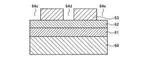
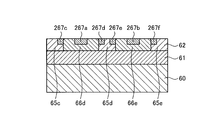
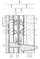
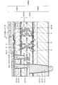
- FIGS. 11B to 11F are cross-sectional views showing a method of manufacturing the first wiring layer according to the second embodiment in the CC'cross section shown in FIG. 11A.
- examples of each manufacturing process will be described with reference to FIGS. 11B to 11F.
- the process of forming an insulating film on the semiconductor substrate is shown. This is, for example, a step of forming the semiconductor substrate 20018 of FIG. 3 and the insulating layer 200025 of the wiring layer 20050. Specifically, as shown in FIG. 11B, the protective insulating film 61 and the interlayer insulating film 62 are formed on the semiconductor substrate 60 on which the element is formed. The details may be the same as the steps described with reference to FIG. 6B in the first embodiment.
- a mask 63 having desired openings 64c, 64d, 64e is formed above the interlayer insulating film 62.
- a resist mask or a hard mask can be used for the mask 63.
- the process of changing the relative permittivity of the insulating film from the opening is shown. Specifically, as shown in FIG. 11D, the exposed regions 65c, 65d, 65e of the interlayer insulating film 62 exposed from the openings 64c, 64d, 64e are changed. For example, the state of the exposed regions 65c, 65d, 65e is changed by performing ion implantation or ashing from the openings 64c, 64d, 64e. As a result, the relative permittivity of the exposed regions 65c, 65d, 65e of the interlayer insulating film 62 can be changed with respect to the relative permittivity of the shielding regions 66d, 66e covered with the mask 63.
- the specific method for changing the state of the exposed regions 65c, 65d, and 65e may be the same as the method described with reference to FIG. 6D in the first embodiment.
- the relative permittivity of the exposed regions 65c, 65d, 65e can be changed with respect to the relative permittivity of the shielding regions 66d, 66e covered with the mask 63.
- the relative permittivity of the exposed regions 65c, 65d, 65e can be made higher than the relative permittivity of the shielding regions 66d, 66e.
- Examples of other state changes of the exposed regions 65c, 65d, and 65e may be the same as the state change examples described with reference to FIG. 6D in the first embodiment.
- the regions 212c and 412c of FIG. 11A correspond to the shielding regions 66d and 66e, respectively.
- the regions 212c and 412c can maintain the state of the film-formed insulating film.
- the regions 212c and 412c can be partially maintained at a low dielectric constant.
- the regions not included in the regions 212c and 412c of FIG. 11A correspond to the exposed regions 65c, 65d, and 65e, respectively.
- the left side region of the region 202a that is not included in the region 212c corresponds to the exposed region 65c
- the region between the region 212c and the region 412c corresponds to the exposed region 65d
- the region 402a corresponds to the exposed area 65e.
- the process of removing the mask on the insulating film is shown. Specifically, as shown in FIG. 11E, the mask 63 is peeled off. After that, in order to stabilize the surface of the interlayer insulating film 62 on the side where the mask is formed, annealing may be performed arbitrarily.
- desired wirings 267a to 267f are formed on the interlayer insulating film 62.
- Conductive materials are used for the wirings 267a to 267f.
- metal materials such as copper (Cu), tungsten (W), and aluminum (Al) can be used.
- Cu copper
- W tungsten
- Al aluminum
- a damascene process is used to open the region forming the wirings 267a to 267f, form copper, and flatten the surface to flatten the wiring 267a.
- ⁇ 267f is formed.
- FIG. 11F shows a step of forming wirings 267a and 267b in the shielding regions 66d and 66e, respectively, and wirings 267c to 267f in the exposed regions 65c, 65d and 65e, respectively.
- the FD wirings 201 and 401 in FIG. 11A correspond to the wirings 267a and 267b, respectively.
- the transfer gate wirings 223a, 224a, 423a, and 424a correspond to the wirings 267c, 267d, 267e, and 267f, respectively.
- the regions 212c and 412c in which the FD wirings 201 and 401 are formed are the shielding regions 66d and 66e, the dielectric constant remains low. Therefore, the capacity can be partially reduced in the vicinity of the FD wirings 201 and 401. Thereby, for example, the wiring capacity of the FD wirings 201 and 401 can be reduced. For example, by reducing the wiring capacitance of the FD wiring, the electromotive force with respect to the number of electrons generated by the photodiode (not shown) increases. As a result, the charge-voltage conversion efficiency in the floating diffusion layer FD is increased.
- the charge-voltage conversion efficiency (gain) in the amplification transistor 53 in which the charge held by the floating diffusion layer FD is input to the gate electrode is increased.
- the electric charge can be detected with high sensitivity even when the electric charge generated by the photoelectric conversion by the photodiode is small, such as in an image in a dark place where the amount of light is small.
- the regions where the transfer gate wirings 223a, 224a, 423a, and 424a are formed are exposed regions 65c, 65d, and 65e, so that the dielectric constant is high. Therefore, the wiring capacity of at least a part of the transfer gate wiring can be increased.
- the areas 212c and 412c are not limited to the configuration shown in FIG. 11A. For example, it may be at least a part of the region shown in FIG. 11A. Alternatively, for example, only the region where the region 212c and the region 202a shown in FIG. 11A overlap may be used.
- the regions 212c and 412c of FIG. 7A correspond to the shielding regions 66d and 66e of FIGS. 11D to 11F, respectively, but the present invention is not limited to this.
- the shielding regions 66d and 66e do not have to be adjacent pixel sharing units like the regions 212c and 412c, and the exposure region 65a and the shielding region 66a may be formed in at least a part of the solid-state image sensor 10.
- the region to which the state change is applied as the exposed regions 65c, 65d, and 65e may be between the regions of the first wiring layer corresponding to the respective light receiving portions of the adjacent pixel sharing units.
- the region between the regions 202a and 402a may be the exposed region 65d.
- wirings other than the FD wirings 201 and 401 can be formed in the shielding areas 66d and 66e. For example, it is possible to form wiring for which the wiring capacity is to be reduced, if necessary.
- wirings other than the transfer gate wirings 221a to 224a and 421a to 424a can be formed in the exposed areas 65c, 65d, 65e. For example, it is possible to form the wiring to which the additional capacity is to be added, if necessary.
- the exposed regions 65c, 65d, 65e and the shielding regions 66d, 66e can be appropriately changed by controlling the forming region of the mask 63 in the step of forming the opening on the insulating film. .. Further, also in the step of changing the relative permittivity of the exposed regions 65c, 65d, 65e, the relative permittivity can be changed to a desired value by controlling conditions such as the dose amount and ion energy at the time of ion implantation. it can.
- the present embodiment can be similarly applied not only to the first wiring layer shown in FIG. 11F but also to the second wiring layer.
- the vertical signal line VSL for transmitting a pixel signal the wiring for transmitting a transistor drive signal, and the like, it is possible to appropriately create wiring for which the capacitance is desired to be reduced and wiring for which the capacitance is to be added.
- the dielectric constant of at least a part of the interlayer insulating film 62 around the wiring is changed by a simple process method.
- the wiring capacity can be partially increased or decreased, so that the charge-voltage conversion efficiency in the floating diffusion layer FD can be increased by reducing the FD capacity, and the desired wiring capacity can be increased. It is possible to manufacture the CMOS image sensor 10 which exhibits various effects depending on the purpose, such as speeding up the operation due to the increase, by a simple manufacturing process.
- FIG. 12 is a plan view showing a plan structure example of a first wiring layer of one pixel sharing unit according to the third embodiment. Specifically, in the solid-state image sensor as shown in FIG. 3, a plan view of the first wiring layer provided on the semiconductor substrate 20001 side among the wiring 20051 included in the wiring layer 20050 is shown. The details may be the same as the configuration described with reference to FIGS. 5B and 6A in the first embodiment described above.
- the regions 202a and 202b have been described in FIG. 6A in correspondence with the exposed regions 65a and 65b.
- the regions 212d, 212e, 212f and 212g in FIG. 12 correspond to the exposed regions 65a and 65b.
- the example of each manufacturing process may be the same as each manufacturing process described with reference to FIGS. 6B to 6F in the first embodiment.
- the region 212d indicates a region including the FD wiring 201 of the first wiring layer and the interlayer insulating film 62 in the vicinity thereof.
- the region 212d is a region between the transfer gate wirings 221a and 222a in the pixel sharing unit 110, as shown in FIG.
- the region 212d includes a part of the FD wiring 201 located between the transfer gate wirings 221a and 222a and a part of the interlayer insulating film 62.
- the region 212e indicates a region including the FD wiring 201 of the first wiring layer and the interlayer insulating film 62 in the vicinity thereof.
- the region 212e is a region between the transfer gate wirings 223a and 224a in the pixel sharing unit 110, as shown in FIG.
- the region 212e includes a part of the FD wiring 201 located between the transfer gate wirings 223a and 224a and a part of the interlayer insulating film 62.
- the region 212f indicates a region including the FD wiring 201 of the first wiring layer and the interlayer insulating film 62 in the vicinity thereof.
- the region 212f is a region between the transfer gate wirings 225a and 226a in the pixel sharing unit 110, as shown in FIG.
- the region 212f includes a part of the FD wiring 201 located between the transfer gate wirings 225a and 226a and a part of the interlayer insulating film 62.
- the region 212g indicates a region including the FD wiring 201 of the first wiring layer and the interlayer insulating film 62 in the vicinity thereof.
- the region 212g is a region between the transfer gate wirings 227a and 228a in the pixel sharing unit 110, as shown in FIG.
- the region 212g includes a part of the FD wiring 201 located between the transfer gate wirings 227a and 228a and a part of the interlayer insulating film 62.
- At least a part of the regions 212d to 212g corresponds to at least a part of the exposed regions 65a and 65b shown in FIGS. 6D to 6F.
- the region 212d corresponds to the exposed region 65a.
- the interlayer insulating film 62 in the vicinity of the FD wiring 201 can have a high dielectric constant. As a result, the wiring capacity of the region 212d can be partially increased.
- FIG. 6F shows a step of forming wirings 67a and 67b in the exposed areas 65a and 65b, respectively.
- the FD wiring 201 of FIG. 12 corresponds to the wiring 67a.
- the region of the interlayer insulating film 62 in the vicinity of the FD wiring 201 that is in contact with the FD wiring 201 from the direction parallel to and perpendicular to the first surface can be partially increased in dielectric constant.
- the wiring capacity of, for example, the FD wiring 201 can be increased. By increasing the wiring capacity of the FD wiring, it is possible to store more charges generated by the photodiode (not shown).
- charge accumulation is performed using the wiring capacitance formed in the high dielectric constant exposed region 65a in FIG. 6F.
- the amount can be increased. This can contribute to the expansion of the dynamic range, that is, the increase in the number of saturated accumulated charges.
- the region 212d by adding the above-mentioned state change to the region 212d, it is possible to increase the dielectric constant of a part of the interlayer insulating film 62 located between the transfer gate wirings 221a and 222a, for example. As a result, the wiring capacity of the region 212d can be partially increased.
- the transfer gate wiring 221a is formed by partially increasing the dielectric constant in the vicinity of the FD wiring 201 and a part of the interlayer insulating film 62 located between the transfer gate wirings 221a and 222a.
- the additional capacity between the FD wiring 201 and the FD wiring 201 can be increased.
- the regions 212d to 212f may have a low dielectric constant by the same method as in the above-described embodiment. Specifically, by controlling the formation region of the mask 63 and the state change such as ion implantation and ashing, the regions 212d to 212f are made to have a lower dielectric constant than the other regions. As a result, a part of the FD wiring is formed in the region of low dielectric constant, and the FD capacitance can be partially reduced. As a result, for example, the charge-voltage conversion efficiency (gain) in the amplification transistor 53 in which the charge held by the floating diffusion layer FD is input to the gate electrode is increased.
- region 212d has been described as an example in FIG. 12, the same configuration may be applied to the regions 212e to 212g. Further, the regions 212d to 212 g are not limited to the range shown in FIG.
- the dielectric constant of at least a part of the interlayer insulating film 62 around the wiring is changed by a simple process method as in the second embodiment.
- the wiring capacity can be partially increased or decreased. Therefore, the dynamic range is expanded by increasing the FD capacity, and the charge-voltage in the floating diffusion layer FD is reduced by reducing the FD capacity.
- FIG. 13A is a plan view showing a plan structure example of a third wiring layer of one pixel sharing unit according to the fourth embodiment. Specifically, in the solid-state image sensor as shown in FIG. 3, among the wiring 20051 included in the wiring layer 20050, the semiconductor substrate 20001 is next to the first wiring layer shown in FIG. 5B and the second wiring layer shown in FIG. 5C. The plan view with the 3rd wiring layer provided on the side is shown.
- the details of the pixel sharing unit 110 shown in FIG. 13A may be the same as the configuration described with reference to FIGS. 5A to 5C in the first embodiment described above.
- the region 204a corresponds to the first light receiving portion 21 in FIG. 5A and the region 202a in FIG. 5B and the region 203a in FIG. 5C in the substrate thickness direction of the semiconductor substrate 20018, and the region 204b is in the same direction in FIG. 5A. It corresponds to the second light receiving unit 22, the region 202b in FIG. 5B, and the region 203b in FIG. 5C.
- the third wiring layer has, for example, wirings 231a to 231e.
- the wirings 231a to 231e include, for example, wiring used as a vertical signal line VSL for transmitting a pixel signal, wiring for transmitting a transistor drive signal, and the like.
- the vertical signal line VSL is shown as wiring 231b in FIG. 13A.
- Region 214 indicates a region including the wiring 231b of the third wiring layer and the interlayer insulating film 62 in the vicinity thereof.
- the area 214 is an area between the wiring 231a and the wiring 231c in the pixel sharing unit 110.
- the region 214 includes a part of the wiring 231a and 231c, at least a part of the wiring 231b located between the wirings 231a and 231c, and at least a part of the interlayer insulating film 62.
- FIGS. 13B to 13D are cross-sectional views showing a method of manufacturing a third wiring layer according to a fourth embodiment in the DD'cross section shown in FIG. 13A.
- examples of each manufacturing process will be described with reference to FIGS. 13B to 13D.
- examples of each manufacturing process of the 1st wiring layer and the 2nd wiring layer which concerns on this Embodiment are each manufacturing described with reference to FIGS. 6B to 6F and FIG. 7B to 7F in the said 1st Embodiment. It may be the same as the process.
- a step of forming the first wiring layer and the second wiring layer will be shown. Specifically, as shown in FIG. 13B, a first wiring layer 701 having an interlayer insulating film 611, a wiring 612, and a protective insulating film 613 is formed on the semiconductor substrate 610. Subsequently, a second wiring layer 702 having an interlayer insulating film 614, a wiring 615, and a protective insulating film 616 is formed on the first wiring layer 701.
- the interlayer insulating films 611 and 614 are formed of, for example, a silicon oxide film (SiO 2 ).
- the protective insulating films 613 and 616 are formed of, for example, a silicon nitride film (SiN).
- FIG. 13B shows a configuration in which the protective insulating films 613 and 616 are provided
- a configuration in which the protective insulating films 613 and 616 are not provided is also possible.
- the interlayer insulating films 611 and 614 a desired insulating film such as a silicon oxide film (SiO 2 ) or a carbon-added silicon oxide film (SiOC) can be used.
- SiO 2 silicon oxide film
- SiOC carbon-added silicon oxide film
- an interlayer insulating film 617 is formed on the second wiring layer 702.
- a film material having a lower dielectric constant than that of the silicon oxide film (SiO 2 ), such as a carbon-added silicon oxide film (SiOC), can be used.
- a mask 618 having a desired opening 641 is formed above the interlayer insulating film 617.
- a resist mask or a hard mask can be used for the mask 618.
- the process of changing the relative permittivity of the insulating film from the opening is shown.
- the exposed region 620a of the interlayer insulating film 617 exposed from the opening 641 is changed.
- the state of the exposed region 620a is changed by performing ion implantation or ashing from the opening 641.
- the relative permittivity of the exposed region 620a of the interlayer insulating film 617 can be changed with respect to the relative permittivity of the shielding region 621 covered with the mask 618.
- the region 214 in FIG. 13A corresponds to the exposed region 620a in FIG. 13B.
- the area other than the area 214 in FIG. 13A corresponds to the shielding area 621 in FIG. 13B.
- the process of removing the mask on the insulating film is shown. Specifically, as shown in FIG. 13C, the mask 618 is peeled off. After that, in order to stabilize the surface of the interlayer insulating film 617 on the side where the mask is formed, annealing may be performed arbitrarily.
- desired wirings 231a to 231e are formed on the interlayer insulating film 617.
- Conductive materials are used for the wirings 231a to 231e.
- metal materials such as copper (Cu), tungsten (W), and aluminum (Al) can be used.
- Cu copper
- W tungsten
- Al aluminum
- a damascene process is used to open the region where the wirings 231a to 231e are formed, to form copper, and to flatten the surface of the wiring 231a.
- ⁇ 231e is formed.
- the third wiring layer 703 having the interlayer insulating film 617 and the wirings 231a to 231e is formed.
- a protective insulating film and the fourth wiring layer and subsequent layers may be further formed.
- FIG. 13D a part of the wiring 231a, the wiring 231b, and a part of the wiring 231c are formed in the exposed area 620a, and a part of the wiring 231a, a part of the wiring 231c, the wiring 231d, and the wiring 231d are formed in the shielding area 621.
- the step of forming 231e is shown. As a result, specifically, the region of the interlayer insulating film 617 in the vicinity of the wiring 231b that is in contact with the wiring 231b from the direction parallel to and perpendicular to the first surface can be partially increased in dielectric constant.
- the wiring capacity of the FD wirings 201 and 401 can be increased.
- the wiring capacity of the FD wiring it is possible to store more charges generated by the photodiode (not shown).
- the wiring capacitance formed in the exposed regions 65a and 65b of high dielectric constant in FIG. 6F is used.
- the amount of charge accumulation can be increased. This can contribute to the expansion of the dynamic range, that is, the increase in the number of saturated accumulated charges.
- FIG. 13B shows an example in which a state change is applied to the entire interlayer insulating film 617 in the film thickness direction to form an exposed region 620a, but the state change occurs in a part of the interlayer insulating film 617 in the film thickness direction.
- the exposed region 620b can be formed by controlling the state change according to the film thickness forming the wirings 231a to 231e.
- the region in contact with the wiring 231a from a direction parallel to the first surface of the semiconductor substrate 610 (same as the first surface of the semiconductor substrate 20018) is increased in dielectric constant. can do.
- the capacity between the wirings in the horizontal direction with respect to the first surface of the semiconductor substrate 610 in the exposed region 620b of FIG. 13E can be increased.
- a part of the region on the second wiring layer 702 side can be controlled so as not to cause a state change, and thus is included in the second wiring layer 702. It is also possible to suppress a change in capacitance between the wiring 615 and the wirings 231a to 231e included in the third wiring layer 703 in the direction perpendicular to the first surface of the semiconductor substrate 610.
- FIG. 13E shows an example in which the state change applied to the interlayer insulating film 617 is controlled to a film thickness equivalent to that of the wirings 231a to 231e, but the present invention is not limited to this.
- the present invention is not limited to this.
- by controlling the amount of energy and the amount of dose of ion implantation it is possible to change the state to a desired depth and form a desired exposed region 620a.
- the region 214 of FIG. 13A has been described as an exposed region 620a, and the other regions have been described as a shielding region 621. Good.
- the exposure and the shielding can be formed in reverse in the exposed area 620a and the shielding area 621.
- the exposure and the shielding can be formed in reverse in the exposed area 620a and the shielding area 621.
- an exposed area is formed at the position of the shielding area 621 instead of the shielding area 621, and the exposed area is located at the position of the exposed area 620a.
- a shielding region may be formed instead of the exposed region 620a.
- the exposed region (substitute for the shielding region 621) can be changed to a high dielectric constant, and the exposed region (substitute for the shielding region 621) can be changed.
- the shielded region (instead of the exposed region 620a) can maintain a low dielectric constant.
- the capacity of the wiring 231b formed in the low dielectric constant region can be partially reduced.
- the wiring capacitance of the wiring 231b it is possible to speed up signal amplification and other operations for the electric charge read from the photodiode.
- the wiring capacity of the wirings 231d and 231e formed in the exposed area (instead of the shielding area 621) can be partially increased.
- the third wiring layer 703 has been described as an example in the present embodiment, the number of wiring layers formed and the application portion of the present embodiment may have a desired configuration as needed.
- the dielectric constant of at least a part of the interlayer insulating film 62 around the wiring is changed by a simple process method.
- the wiring capacity can be partially increased or decreased, so that the dynamic range can be expanded by increasing the wiring capacity of the vertical signal line VSL and the wiring capacity of the vertical signal line VSL can be reduced. It is possible to manufacture the CMOS image sensor 10 that exhibits various effects according to the purpose, such as high-speed operation by the above, high-speed operation by increasing or decreasing the capacity of the desired wiring, and / or addition of functions, by a simple manufacturing process. Become.
- FIG. 14A and FIG. 14B are cross-sectional views showing a method of manufacturing a semiconductor device according to the fifth embodiment.
- a protective insulating film 61 and an interlayer insulating film 62 are formed on the semiconductor substrate 60, and a mask 63 having a desired opening 642 is formed on the protective insulating film 61.
- the interlayer insulating film 62 has an exposed region 621a corresponding to the opening 642 and shielding regions 621b and 621c corresponding to the forming region of the mask 63.
- Other configurations and details may be the same as those described with reference to FIGS. 6D, 7D, 11D, and 13B in the first embodiment, for example.
- a desired state change is given to the exposed region 621a exposed from the opening 642.
- ion implantation or ashing is performed from the opening 642 to partially increase the dielectric constant of the interlayer insulating film 62 formed of the low dielectric constant material film.
- the film thickness of the exposed region 621a may be thinner than the film thickness of the shielding regions 621b and 621c. This occurs, for example, because the pores of the interlayer insulating film 62 are reduced by ion implantation or ashing, and the film density of the interlayer insulating film is increased, so that the exposed region 621a is compressed more than the shielding regions 621b and 621c. ..
- Wiring 671a, 671b, 671c are formed in the exposed area 621a and the shielding area 621b, 621c formed in FIG. 14A, respectively.
- Other configurations and details may be the same as those described with reference to FIGS. 6F, 7F, 11F, 13D, and 13E in the first embodiment, for example.
- the position where the wiring 671a is formed may be formed at a position closer to the semiconductor substrate 60 side than the wirings 671b and 671c.
- a part of the surface of the wiring 671a on the semiconductor substrate 60 side may be formed on the semiconductor substrate 60 side rather than a part of the surface of the wiring 671b or 671c on the semiconductor substrate 60 side.
- the exposed region 621a is compressed and thinned by the state change given to the exposed region 621a, so that the surface of the exposed region 621a opposite to the semiconductor substrate 60 (fourth surface) This is because it is closer to the semiconductor substrate 60 than that of the shielding regions 621b and 621c (fifth surface).
- the change amount ⁇ d2-d3 of the formation position of the wiring 671a in the film thickness direction may be substantially the same or the same degree of change.
- the position d0 indicates the height of the upper surface of the shielding regions 621b and 621c and the wirings 671b and 671c from the first surface of the semiconductor substrate 60 (this is referred to as the upper surface in this description).
- the position d1 indicates the height of the exposed region 621a and the upper surface of the wiring 671a from the upper surface (first surface) of the semiconductor substrate 60.
- the position d2 indicates the height of the lower surfaces of the wirings 671b and 671c from the upper surface (first surface) of the semiconductor substrate 60.
- the position d3 indicates the height of the lower surface of the wiring 671a from the upper surface (first surface) of the semiconductor substrate 60.
- the amount of change ⁇ d0 ⁇ d1 is a part of the shielding region 621b or 621c on the surface of the interlayer insulating film 62 opposite to the semiconductor substrate 60 side in the direction perpendicular to the first surface of the semiconductor substrate 60.
- the difference between the formation position and a part of the formation position of the exposed region 621a is shown.
- the amount of change ⁇ d2-d3 is the formation position of a part of the surface of the wiring 671a on the semiconductor substrate 60 side and the surface of the wiring 671b or 671c on the semiconductor substrate 60 side in the direction perpendicular to the first surface of the semiconductor substrate 60. The difference from the formation position with a part of is shown.
- the upper surface of the exposed area 621a does not necessarily have to be flat as shown in FIG. 14A.
- unevenness may be formed on the upper surface of the exposed region 621a because the state change due to ion implantation or ashing is partially non-uniform.
- state changes may be formed in multiple stages.
- the four corners of the exposed region 621a at the boundary with the shielding regions 621b and 621c may be rounded.
- the upper surface of the interlayer insulating film 62 may be flattened after the forming step of FIG. 14A.
- the mask 63 may be removed to flatten the upper surfaces of the exposed region 621a and the shielding regions 621b and 621c.
- the shielding regions 621b and 621c may be polished so as to have the same film thickness as the exposed region 621a.
- the above-mentioned change amount ⁇ d0 ⁇ d1 can be substantially zero.
- the interlayer insulating film 62 and / or the wirings 671a, 671b, 671c may be flattened.
- the step of flattening the exposed area 621a, the shielding area 621b, 621c, the wiring 671a, 671b, 671c is performed. You may go.
- the exposed area 612a, the shielding area 621b, and 621c may be polished so as to have the same film thickness as the exposed area 621a.
- the wiring 671a, 671b, 671c so that the surface of the wiring 671a opposite to the semiconductor substrate 60 side and the position of the surface of the wiring 671b, 671c opposite to the semiconductor substrate 60 side are at the same height.
- At least a part of the exposed area 621a and the shielding area 621b, 621c may be polished.
- the second surface of the wiring 671a on the semiconductor substrate 60 side is the semiconductor of the wirings 671b, 671c. It may be formed at a position closer to the semiconductor substrate 60 than the second surface on the substrate 60 side.
- the above-mentioned change amount ⁇ d0 ⁇ d1 may be zero, while the change amount ⁇ d2-d3 may be zero or more.
- the dielectric constant of at least a part of the interlayer insulating film 62 around the wiring is changed by a simple process method.
- the CMOS image sensor 10 is designed and manufactured by changing the film thickness of the interlayer insulating film 62 and the formation position of the wiring according to the region and exhibiting various effects according to the purpose. It becomes possible to do.
- FIG. 15 is a block diagram showing a schematic configuration example of the semiconductor device according to the sixth embodiment. In the following description, a case where the above-described embodiment is applied to a solid-state image sensor which is a semiconductor device will be illustrated.
- the solid-state image sensor 1010A to which the above-described embodiment can be applied includes, for example, a structure in which a sensor substrate 1020 and a circuit board 1030 are vertically laminated.
- the above-described embodiment can be applied to the wiring layer of the sensor substrate 1020 and / or the circuit board 1030 of FIG. Further, it can be applied to a semiconductor device constituting each block such as an analog-to-digital converter (AD converter) 1050 of the signal processing unit 1031 included in the circuit board 1030 and a memory unit 1032. Details of each block included in the circuit board 1030 will be described later.
- AD converter analog-to-digital converter
- the sensor substrate 1020 shown in FIG. 15 includes, for example, a sensor unit 1021 and a row selection unit 1025.
- the sensor unit 1021 has a plurality of sensors 1040 arranged in a matrix.
- the sensor 1040 includes, for example, a photodiode 1041, a transfer transistor (also referred to as a transfer gate) 1042, a reset transistor 1043, an amplification transistor 1044, a selection transistor 1045, and a stray diffusion region (FD) 1046.
- the row selection unit 1025 selects each sensor 1040 of the sensor unit 1021 in units of rows based on the address signal given from the circuit board 1030 side. Although the row selection unit 1025 is provided on the sensor board 1020 here, it can also be provided on the circuit board 1030.
- the circuit board 1030 shown in FIG. 15 includes, for example, a signal processing unit 1031, a memory unit 1032, a data processing unit 1033, a control unit 1034, a current source 1035, a decoder 1036, a row decoder 1037, an interface (IF) unit 1038, and the like. ..
- a sensor drive unit (not shown) for driving each sensor 1040 of the sensor unit 1021 is provided.
- the signal processing unit 1031 receives, for example, a predetermined signal including digitization (AD conversion) in parallel (column parallel) for each sensor row with respect to the analog signal read from each sensor 1040 of the sensor unit 1021 for each sensor row. It can be configured to perform processing.
- the signal processing unit 1031 has an analog-to-digital converter (AD converter) 1050 that digitizes the analog signal read from each sensor 1040 of the sensor unit 1021 to the signal line 1026, and is subjected to AD conversion.
- the image data (digital data) is transferred to the memory unit 1032.
- a row control line is wired for each sensor row and a column signal line (vertical signal line) is wired for each sensor row to the sensor unit 1021 in which the sensors 1040 are arranged in a matrix.
- the signal processing unit 1031 may further have a reference voltage generation unit 1054 that generates a reference voltage used for AD conversion by the AD converter 1050.
- the reference voltage generator 1054 can be configured by using, for example, a DA converter (digital-analog converter), but is not limited thereto.
- the AD converter 1050 has, for example, a comparator 1051 and a counter unit 1052.
- the comparator 1051 compares both inputs by using an analog signal read from each sensor 1040 of the sensor unit 1021 via the signal line 1026 as a comparison input and a reference voltage supplied from the reference voltage generation unit 1054 as a reference input.
- As the counter unit 1052 for example, an up / down counter is used.
- the clock CK is given to the counter unit 1052 at the same timing as the supply start timing of the reference voltage to the comparator 1051.
- the counter unit 1052 which is an up / down counter, performs a down count or an up count in synchronization with the clock CK to perform a comparison operation from the period of the pulse width of the output pulse of the comparator 1051, that is, from the start of the comparison operation. Measure the comparison period until the end of. Then, the count result (count value) of the counter unit 1052 becomes a digital value (image data) obtained by digitizing the analog signal.
- the data latch unit 1055 latches the image data digitized by the AD converter 1050.
- the memory unit 1032 stores image data that has undergone predetermined signal processing in the signal processing unit 1031.
- the data processing unit 1033 reads the image data stored in the memory unit 1032 in a predetermined order, performs various processes, and outputs the image data to the outside of the chip via the interface (IF) 1038.
- the control unit 1034 includes a sensor drive unit (not shown), a memory unit 1032, and data processing based on reference signals such as a horizontal synchronization signal XHS, a vertical synchronization signal XVS, and a master clock MCK given from outside the chip. It controls each operation of the signal processing unit 1031 such as unit 1033. At this time, the control unit 1034 synchronizes the circuit on the sensor board 1020 side (row selection unit 1025 and sensor unit 1021) with the signal processing unit 1031 (memory unit 1032, data processing unit 1033, etc.) on the circuit board 1030 side. Control while taking.
- the current source 1035 is connected to, for example, each of the signal lines 1026 from which analog signals are read out for each sensor row from each sensor 1040 of the sensor unit 1021.
- the current source 1035 has, for example, a so-called load MOS circuit configuration including MOS transistors whose gate potential is biased to a constant potential so as to supply a constant current to the signal line 1026.
- the current source 1035 composed of this load MOS circuit operates the amplification transistor 1044 as a source follower by supplying a constant current to the amplification transistor 1044 of the sensor 1040 included in the selected row.
- the decoder 1036 When the decoder 1036 selects each sensor 1040 of the sensor unit 1021 in line units under the control of the control unit 1034, the decoder 1036 gives an address signal for designating the address of the selected line to the line selection unit 1025.
- the line decoder 1037 specifies a line address when writing image data to the memory unit 1032 and reading image data from the memory unit 1032 under the control of the control unit 1034.
- the sensor board 1020 and the circuit board 1030 are electrically connected via a connection portion such as a TSV (Through-Silicon Via) that penetrates the semiconductor board.
- Connections using TSVs include, for example, the so-called Twin TSV method in which two TSVs, a TSV provided on the sensor board 1020 and a TSV provided from the sensor board 1020 to the circuit board 1030, are connected on the outer surface of the chip, or a sensor.
- a so-called Shared TSV method or the like in which both are connected by a TSV penetrating from the substrate 1020 to the circuit board 1030 can be used.
- the sensor board 1020 and the circuit board 1030 are electrically connected via a connection portion such as a so-called metal joint in which electrode pads formed on the joint surfaces of each other are bonded to each other.
- the electrode pad is made of a metal such as copper and is also called a Cu-Cu bond.
- bump bonding or the like can be used for the connection portion between the sensor board 1020 and the circuit board 1030.
- each block described in the sensor substrate 1020 and the circuit board 1030 may be provided on the same semiconductor substrate.
- each block of the row selection unit 1025 and the circuit board 1030 may be formed in a peripheral region other than the region where the sensor unit 1021 is formed.
- an application example in a stacked solid-state image sensor is shown, but the present invention is not limited to this, and can be applied to a semiconductor device in which each block is independently configured.
- the above-described embodiment can be applied to an analog element of a circuit or memory that independently configures the AD converter 1050 and the memory unit 1032.
- the dielectric constant of at least a part of the interlayer insulating film 62 around the desired wiring constituting the semiconductor device is changed by a simple process method.
- FIG. 16 is a circuit diagram showing a schematic configuration example of a unit pixel of the solid-state image sensor according to the seventh embodiment. Specifically, it is a modification of the circuit diagram showing a schematic configuration example of the unit pixel 50 of FIG.
- the switching transistor 2001 is added to the circuit diagram showing the schematic configuration example of the unit pixel 50 in FIG.
- the source of the switching transistor 2001 is connected to, for example, the source of the reset transistor 52.
- the switching transistor 2001 is turned on by the signal input from the switching transistor drive line LD2003, the sub-capacity section 2003 is added in addition to the main capacitance section 2002 of the floating diffusion layer FD.
- the FD capacity can be increased.
- the configuration of the sub-capacity unit 2003 can be realized by applying a configuration in which the FD capacity is increased by the wiring capacity, for example, as in the above-described embodiment.
- the switching transistor 2001 is operated as a transistor for switching the conversion efficiency (gain) of the floating diffusion layer FD, and the capacitance of the floating diffusion layer FD is made variable.
- the switching transistor 2001 is provided in the region of the first transistor group 31 and / or the second transistor group 32 shown in FIG. 5A.
- a switch gate (also referred to as an FD gate) of the switching transistor 2001 is provided in a desired region of the first transistor group 31 and / or the second transistor group 32.
- the second reset gate 14b shown in FIG. 5A can be replaced with the switch gate of the switching transistor 2001 of FIG.
- the switch gate wiring (also referred to as FD gate wiring) of the switching transistor 2001 is provided in the first wiring layer shown in FIG. 5B so as to correspond to FIG. 5A.
- the gate electrode of the switching transistor 2001 can be formed in a desired region of FIG. 5B corresponding to the first transistor group 31 and / or the second transistor group 32 shown in FIG. 5A.
- the second reset gate wiring 114b shown in FIG. 5B can be replaced with the switch gate wiring of the switching transistor 2001 of FIG.
- the source of the switching transistor 2001 is wired so as to be connected to the source of the reset transistor 52.
- the switching transistor drive line LD2003 included in the pixel drive line LD is connected to the gate of the switching transistor 2001.
- the source of the switching transistor 2001 is electrically connected to the floating diffusion layer FD.
- the auxiliary capacitance unit 2003 which is an additional capacitance that can be used as the FD capacitance, becomes effective. Therefore, the stray diffusion layer FD is composed of, for example, a parasitic capacitance of the reset transistor 52 itself, a main capacitance portion 2002 which is a diffusion capacitance, and a subcapacity portion 2003 which is a wiring capacitance.
- the auxiliary capacitance section 2003 By connecting the auxiliary capacitance section 2003 to the floating diffusion layer FD, the FD capacitance can be expanded and a larger amount of electric charge generated by the photodiode can be stored.
- the amount of charge generated by photoelectric conversion with a photodiode increases, such as when imaging in a bright place with a large amount of light
- the amount of charge accumulation can be increased by using the wiring capacity as in the above embodiment. ..
- it can contribute to the expansion of the dynamic range, that is, the increase in the number of saturated accumulated charges.
- the stray diffusion layer FD is composed of, for example, the parasitic capacitance of the reset transistor 52 itself and the main capacitance portion 2002 which is the diffusion capacitance.
- the auxiliary capacitance unit 2003 which is an additional capacitance that can be used as the FD capacitance, can be enabled or disabled. Specifically, the capacity of the floating diffusion layer FD can be expanded or contracted. As a result, a desired FD capacitance can be used according to the amount of light and the amount of charge generated by the photodiode. For example, when the amount of charge generated by photoelectric conversion with a photodiode is large or small, such as when imaging in a place with a large difference in brightness, the above-mentioned switching transistor 2001 is formed to form an appropriate FD capacitance. Can be done. Thereby, the charge-voltage conversion efficiency (gain) of the floating diffusion layer FD can be controlled.
- the auxiliary capacitance unit 2003 when driving in the low conversion efficiency mode, the auxiliary capacitance unit 2003 is enabled by turning on the switching transistor 2001 (inputting a High level signal to the gate).
- the switching transistor 2001 inputting a High level signal to the gate.
- the floating diffusion layer FD holds a large amount of charge, such as when the light is high or when signals generated by a plurality of photodiodes and / or pixels are added by the floating diffusion layer FD
- the low conversion efficiency mode is used.
- the operating range of the vertical signal line VSL can be secured by operating with.
- the auxiliary capacitance unit 2003 when driving in the high conversion efficiency mode, the auxiliary capacitance unit 2003 is invalidated by turning off the switching transistor 2001 (inputting a Low level signal to the gate).
- the signal-to-noise ratio (Signal-Noise Ratio) of the S / N ratio can be increased by operating in the high conversion efficiency mode. Can be done. Therefore, it is possible to reduce the noise for the signal generated by the photodiode and / or the pixel.
- the dielectric constant of at least a part of the interlayer insulating film 62 around the desired wiring constituting the semiconductor device is changed by a simple process method, as in the above-described embodiment.
- there are various configurations depending on the purpose such as adding a capacitance to the floating diffusion layer FD and switching the charge-voltage conversion efficiency by making the capacitance of the floating diffusion layer FD variable. It becomes possible to design and manufacture the CMOS image sensor 10 in which the effect is exhibited.
- FIG. 17 is a diagram showing a layout example of the color filter according to the seventh embodiment. Specifically, regarding CF (color filter) 2012 provided above the photodiode 20001 in FIG. 3, a layout example in a plurality of pixels included in the pixel array unit 11 in FIG. 1 is shown. Note that FIG. 17 shows a layout example of a color filter array when, for example, a color image in the three primary colors of RGB is acquired.
- CF color filter
- a color filter that selectively transmits light of a specific wavelength is arranged for the photodiode PD of each unit pixel 50.
- the color filter array 160 has, for example, a configuration in which a pattern of 2 ⁇ 2 pixels (hereinafter referred to as a unit pattern) 161 which is a unit of repetition in the color filter array is arranged in a two-dimensional grid pattern. Be prepared.
- Each unit pattern 161 includes, for example, a color filter 107R that selectively transmits light having a wavelength component of red (R), a color filter 107G that selectively transmits light having a wavelength component of green (G), and blue ( It is composed of a total of three types of color filters, including a color filter 107B that selectively transmits light having a wavelength component of B).
- a color filter 107R that selectively transmits light having a wavelength component of red (R)
- a color filter 107G that selectively transmits light having a wavelength component of green (G)
- blue It is composed of a total of three types of color filters, including a color filter 107B that selectively transmits light having a wavelength component of B).
- the layout is such that the color filter 107G is arranged in the upper left, the color filter 107R is arranged in the upper right, the color filter 107B is arranged in the lower left, and the color filter 107G is arranged in the lower right.
- the lower right color filter 107G can be used as a color filter that selectively transmits light having a wavelength component of IR light.
- the color filter array 160 of the Bayer array is illustrated, but the base color filter array is not limited to the Bayer array.
- an X-Trans (registered trademark) type color filter array with a unit pattern of 3 ⁇ 3 pixels, a quad Bayer array with 4 ⁇ 4 pixels, and color filters for each of the three primary colors of RGB, as well as broadening the visible light region It is possible to base various color filter arrays such as a 4 ⁇ 4 pixel white RGB type color filter array including a color filter having various light transmission characteristics (hereinafter, also referred to as clear or white). This also applies to other embodiments described later.
- FIG. 18 for explaining the layer structure and layout of the solid-state image sensor according to the above-described embodiment with some examples is shown in FIG. 18 according to the ninth embodiment. It is a figure which shows the outline of the example of the layer structure and layout of.
- FIG. 18A shows a schematic configuration example of the solid-state image sensor when the solid-state image sensor according to the above-described embodiment is a non-stacked type.
- the solid-state image sensor 23010 has one die (semiconductor substrate) 23011 as shown in FIG. 18A.
- the die 23011 includes a pixel region 23012 in which pixels are arranged in an array, a control circuit 23013 for driving pixels and various other controls, and a logic circuit 23014 for signal processing.
- B and C in FIG. 18 show a schematic configuration example of the solid-state image sensor when the solid-state image sensor according to the above-described embodiment is a laminated type.
- the solid-state image sensor 23020 is configured as one semiconductor chip by stacking two dies, a sensor die 23021 and a logic die 23024, and electrically connecting them.
- the sensor die 23021 is equipped with a pixel region 23012 and a control circuit 23013
- the logic die 23024 is equipped with a logic circuit 23014 including a signal processing circuit that performs signal processing.
- the pixel region 23012 is mounted on the sensor die 23021, and the control circuit 23013 and the logic circuit 23014 are mounted on the logic die 23024.
- FIG. 19 is a cross-sectional view showing a first configuration example of the stacked solid-state image sensor illustrated in B and C of FIG.
- the sensor die 23021 is formed with PDs (photodiodes), FDs (floating diffusion), Trs (MOS FETs), and Trs, which are control circuits 23013, that form pixels in the pixel area 23012. Further, the sensor die 23021 is formed with a wiring layer 23101 having a plurality of layers, in this example, three layers of wiring 23110.
- the control circuit 23013 (Tr) can be configured on the logic die 23024 instead of the sensor die 23021.
- a Tr constituting the logic circuit 23014 is formed on the logic die 23024. Further, the logic die 23024 is formed with a wiring layer 23161 having a plurality of layers, in this example, three layers of wiring 23170. Further, the logic die 23024 is formed with a connection hole 23171 having an insulating film 23172 formed on the inner wall surface, and a connection conductor 23173 connected to the wiring 23170 or the like is embedded in the connection hole 23171.
- the sensor die 23021 and the logic die 23024 are attached to each other so that the wiring layers 23101 and 23161 face each other, thereby forming a laminated solid-state image sensor 23020 in which the sensor die 23021 and the logic die 23024 are laminated.
- a film 23191 such as a protective film is formed on the surface on which the sensor die 23021 and the logic die 23024 are bonded.
- the sensor die 23021 is formed with a connection hole 23111 that penetrates the sensor die 23021 from the back surface side (the side where light is incident on the PD) (upper side) of the sensor die 23021 and reaches the wiring 23170 on the uppermost layer of the logic die 23024. Further, the sensor die 23021 is formed with a connection hole 23121 that reaches the first layer wiring 23110 from the back surface side of the sensor die 23021 in the vicinity of the connection hole 23111. An insulating film 23112 is formed on the inner wall surface of the connection hole 23111, and an insulating film 23122 is formed on the inner wall surface of the connection hole 23121. Then, the connecting conductors 23113 and 23123 are embedded in the connecting holes 23111 and 23121, respectively.
- the connecting conductor 23113 and the connecting conductor 23123 are electrically connected to each other on the back surface side of the sensor die 23021, whereby the sensor die 23021 and the logic die 23024 are connected to the wiring layer 23101, the connection hole 23121, the connection hole 23111, and the wiring layer. It is electrically connected via 23161.
- FIG. 20 is a cross-sectional view showing a second configuration example of the stacked solid-state image sensor illustrated in B and C of FIG.
- the sensor die 23021 (wiring layer 23101 (wiring 23110)) and the logic die 23024 (wiring layer 23161 (wiring) are provided by one connection hole 2321 formed in the sensor die 23021. 23170)) is electrically connected.
- connection hole 2321 is formed so as to penetrate the sensor die 23021 from the back surface side of the sensor die 23021 and reach the wiring 23170 on the uppermost layer of the logic die 23024 and reach the wiring 23110 on the uppermost layer of the sensor die 23021. Will be done.
- An insulating film 23212 is formed on the inner wall surface of the connection hole 23211, and a connection conductor 23213 is embedded in the connection hole 23211.
- the sensor die 23021 and the logic die 23024 are electrically connected by the two connection holes 23111 and 23121, but in FIG. 20, the sensor die 23021 and the logic die 23024 are connected by one connection hole 23211. It is electrically connected.
- FIG. 21 is a cross-sectional view showing a third configuration example of the stacked solid-state image sensor illustrated in B and C of FIG.
- the solid-state image sensor 23020 of FIG. 21 has a surface on which the sensor die 23021 and the logic die 23024 are bonded, in that a film 23191 such as a protective film is not formed on the surface on which the sensor die 23021 and the logic die 23024 are bonded. , Different from the case of FIG. 19 in which a film 23191 such as a protective film is formed.
- the sensor die 23021 and the logic die 23024 are overlapped with each other so that the wirings 23110 and 23170 are in direct contact with each other, heated while applying the required load, and the wirings 23110 and 23170 are directly joined. It is composed.
- FIG. 22 is a cross-sectional view showing another configuration example of the stacked solid-state image sensor according to the ninth embodiment.
- the solid-state image sensor 23401 has a three-layer laminated structure in which three dies of a sensor die 23411, a logic die 23412, and a memory die 23413 are laminated.
- the memory die 23413 has, for example, a memory circuit that stores data temporarily required for signal processing performed by the logic die 23421.
- the logic die 23412 and the memory die 23413 are stacked in this order under the sensor die 23411, but the logic die 23412 and the memory die 23413 are arranged in the reverse order, that is, in the order of the memory die 23413 and the logic die 23412. It can be laminated under 23411.
- the sensor die 23411 is formed with a photodiode PD (corresponding to a photodiode 111) that serves as a photoelectric conversion unit of a unit pixel 50, and a source / drain region of a pixel transistor.
- a photodiode PD corresponding to a photodiode 111 that serves as a photoelectric conversion unit of a unit pixel 50, and a source / drain region of a pixel transistor.
- a gate electrode is formed around the photodiode PD via a gate insulating film, and a pixel transistor 23421 and a pixel transistor 23422 are formed by a source / drain region paired with the gate electrode.
- the pixel transistor 23421 adjacent to the photodiode PD is the transfer transistor 51, and one of the paired source / drain regions constituting the pixel transistor 23421 constitutes the floating diffusion layer FD.
- an interlayer insulating film 23435 is formed on the sensor die 23411, and a connection hole is formed on the interlayer insulating film 23435.
- a pixel Tr23421 and a connecting conductor 23431 connected to the pixel Tr23422 are formed in the connection hole.
- the sensor die 23411 is formed with a wiring layer 23433 having a plurality of layers of wiring 23432 connected to each connection conductor 23431.
- an aluminum pad 23434 that serves as an electrode for external connection is formed in the lowermost layer of the wiring layer 23433 of the sensor die 23411. That is, in the sensor die 23411, the aluminum pad 23434 is formed at a position closer to the adhesive surface 23440 with the logic die 23421 than the wiring 23432.
- the aluminum pad 23434 is used as one end of the wiring related to the input / output of a signal to the outside.
- the sensor die 23411 is formed with a contact 23441 used for electrical connection with the logic die 23412.
- the contact 23441 is connected to the contact 23451 of the logic die 23412 and also to the aluminum pad 23442 of the sensor die 23411.
- a pad hole 23443 is formed so as to reach the aluminum pad 23442 from the back surface side (upper side) of the sensor die 23411.
- the contact 23451 formed on the logic die 23412 is also used for electrical connection with the memory die 23413.
- the contact 23451 is connected to the aluminum pad 23461 of the memory die 23413.
- the above-described embodiment can be applied to the configuration of the wiring layer shown in FIGS. 18 to 22.
- FIG. 23 is a block diagram showing a schematic configuration example of an electronic device equipped with a solid-state image sensor to which the technique according to the present disclosure can be applied.
- the electronic device 1 includes, for example, an image pickup lens 20, a solid-state image pickup device 10, a storage unit 30, and a processor 40.
- the image pickup lens 20 is an example of an optical system that collects incident light and forms an image on the light receiving surface of the solid-state image sensor 10.
- the light receiving surface may be a surface on which the photoelectric conversion elements in the solid-state image sensor 10 are arranged.
- the solid-state image sensor 10 photoelectrically converts the incident light to generate image data. Further, the solid-state image sensor 10 executes predetermined signal processing such as noise removal and white balance adjustment on the generated image data.
- the storage unit 30 is composed of, for example, a flash memory, a DRAM (Dynamic Random Access Memory), a SRAM (Static Random Access Memory), or the like, and records image data or the like input from the solid-state imaging device 10.
- the processor 40 may include, for example, an application processor that is configured by using a CPU (Central Processing Unit) or the like and executes an operating system, various application software, or the like, a GPU (Graphics Processing Unit), a baseband processor, or the like.
- the processor 40 executes various processes as necessary for the image data input from the solid-state image sensor 10 and the image data read from the storage unit 30, displays the images to the user, and performs a predetermined network. It is sent to the outside via.
- FIG. 24 is a diagram showing an example of a schematic configuration of an endoscopic surgery system to which the technique according to the present disclosure (the present technique) can be applied.
- FIG. 24 shows a surgeon (doctor) 11131 performing surgery on patient 11132 on patient bed 11133 using the endoscopic surgery system 11000.
- the endoscopic surgery system 11000 includes an endoscope 11100, other surgical tools 11110 such as an abdominal tube 11111 and an energy treatment tool 11112, and a support arm device 11120 that supports the endoscope 11100.
- a cart 11200 equipped with various devices for endoscopic surgery.
- the endoscope 11100 is composed of a lens barrel 11101 in which a region having a predetermined length from the tip is inserted into the body cavity of the patient 11132, and a camera head 11102 connected to the base end of the lens barrel 11101.
- the endoscope 11100 configured as a so-called rigid mirror having a rigid barrel 11101 is illustrated, but the endoscope 11100 may be configured as a so-called flexible mirror having a flexible barrel. Good.
- An opening in which an objective lens is fitted is provided at the tip of the lens barrel 11101.
- a light source device 11203 is connected to the endoscope 11100, and the light generated by the light source device 11203 is guided to the tip of the lens barrel by a light guide extending inside the lens barrel 11101 to be an objective. It is irradiated toward the observation target in the body cavity of the patient 11132 through the lens.
- the endoscope 11100 may be a direct endoscope, a perspective mirror, or a side endoscope.
- An optical system and an image sensor are provided inside the camera head 11102, and the reflected light (observation light) from the observation target is focused on the image sensor by the optical system.
- the observation light is photoelectrically converted by the image sensor, and an electric signal corresponding to the observation light, that is, an image signal corresponding to the observation image is generated.
- the image signal is transmitted as RAW data to the camera control unit (CCU: Camera Control Unit) 11201.
- CCU Camera Control Unit
- the CCU11201 is composed of a CPU (Central Processing Unit), a GPU (Graphics Processing Unit), etc., and comprehensively controls the operations of the endoscope 11100 and the display device 11202. Further, the CCU 11201 receives an image signal from the camera head 11102, and performs various image processes on the image signal for displaying an image based on the image signal, such as development processing (demosaic processing).
- a CPU Central Processing Unit
- GPU Graphics Processing Unit
- the display device 11202 displays an image based on the image signal processed by the CCU 11201 under the control of the CCU 11201.
- the light source device 11203 is composed of, for example, a light source such as an LED (light LED diode), and supplies irradiation light to the endoscope 11100 when photographing an operating part or the like.
- a light source such as an LED (light LED diode)
- the input device 11204 is an input interface for the endoscopic surgery system 11000.
- the user can input various information and input instructions to the endoscopic surgery system 11000 via the input device 11204.
- the user inputs an instruction to change the imaging conditions (type of irradiation light, magnification, focal length, etc.) by the endoscope 11100.
- the treatment tool control device 11205 controls the drive of the energy treatment tool 11112 for cauterizing, incising, sealing a blood vessel, or the like of a tissue.
- the pneumoperitoneum device 11206 uses a gas in the pneumoperitoneum tube 11111 to inflate the body cavity of the patient 11132 for the purpose of securing the field of view by the endoscope 11100 and securing the work space of the operator.
- the recorder 11207 is a device capable of recording various information related to surgery.
- the printer 11208 is a device capable of printing various information related to surgery in various formats such as text, images, and graphs.
- the light source device 11203 that supplies the irradiation light to the endoscope 11100 when photographing the surgical site can be composed of, for example, an LED, a laser light source, or a white light source composed of a combination thereof.
- a white light source is configured by combining RGB laser light sources, the output intensity and output timing of each color (each wavelength) can be controlled with high accuracy. Therefore, the light source device 11203 adjusts the white balance of the captured image. It can be carried out.
- the laser light from each of the RGB laser light sources is irradiated to the observation target in a time-divided manner, and the drive of the image sensor of the camera head 11102 is controlled in synchronization with the irradiation timing to support each of RGB. It is also possible to capture the image in a time-divided manner. According to this method, a color image can be obtained without providing a color filter on the image sensor.
- the drive of the light source device 11203 may be controlled so as to change the intensity of the output light at predetermined time intervals.
- the drive of the image sensor of the camera head 11102 in synchronization with the timing of the change of the light intensity to acquire an image in time division and synthesizing the image, so-called high dynamic without blackout and overexposure. Range images can be generated.
- the light source device 11203 may be configured to be able to supply light in a predetermined wavelength band corresponding to special light observation.
- special light observation for example, by utilizing the wavelength dependence of light absorption in body tissue to irradiate light in a narrow band as compared with the irradiation light (that is, white light) in normal observation, the mucosal surface layer.
- narrow band imaging in which a predetermined tissue such as a blood vessel is photographed with high contrast, is performed.
- fluorescence observation in which an image is obtained by fluorescence generated by irradiating with excitation light may be performed.
- the body tissue is irradiated with excitation light to observe the fluorescence from the body tissue (autofluorescence observation), or a reagent such as indocyanine green (ICG) is locally injected into the body tissue and the body tissue is injected. It is possible to obtain a fluorescence image by irradiating excitation light corresponding to the fluorescence wavelength of the reagent.
- the light source device 11203 may be configured to be capable of supplying narrow band light and / or excitation light corresponding to such special light observation.
- FIG. 25 is a block diagram showing an example of the functional configuration of the camera head 11102 and CCU11201 shown in FIG. 24.
- the camera head 11102 includes a lens unit 11401, an imaging unit 11402, a driving unit 11403, a communication unit 11404, and a camera head control unit 11405.
- CCU11201 has a communication unit 11411, an image processing unit 11412, and a control unit 11413.
- the camera head 11102 and CCU11201 are communicably connected to each other by a transmission cable 11400.
- the lens unit 11401 is an optical system provided at a connection portion with the lens barrel 11101.
- the observation light taken in from the tip of the lens barrel 11101 is guided to the camera head 11102 and incident on the lens unit 11401.
- the lens unit 11401 is configured by combining a plurality of lenses including a zoom lens and a focus lens.
- the image sensor constituting the image pickup unit 11402 may be one (so-called single plate type) or a plurality (so-called multi-plate type).
- each image pickup element may generate an image signal corresponding to each of RGB, and a color image may be obtained by synthesizing them.
- the image pickup unit 11402 may be configured to have a pair of image pickup elements for acquiring image signals for the right eye and the left eye corresponding to 3D (dimensional) display, respectively.
- the 3D display enables the operator 11131 to more accurately grasp the depth of the biological tissue in the surgical site.
- a plurality of lens units 11401 may be provided corresponding to each image pickup element.
- the imaging unit 11402 does not necessarily have to be provided on the camera head 11102.
- the image pickup unit 11402 may be provided inside the lens barrel 11101 immediately after the objective lens.
- the drive unit 11403 is composed of an actuator, and the zoom lens and the focus lens of the lens unit 11401 are moved by a predetermined distance along the optical axis under the control of the camera head control unit 11405. As a result, the magnification and focus of the image captured by the imaging unit 11402 can be adjusted as appropriate.
- the communication unit 11404 is composed of a communication device for transmitting and receiving various information to and from the CCU11201.
- the communication unit 11404 transmits the image signal obtained from the image pickup unit 11402 as RAW data to the CCU 11201 via the transmission cable 11400.
- the communication unit 11404 receives a control signal for controlling the drive of the camera head 11102 from the CCU 11201 and supplies the control signal to the camera head control unit 11405.
- the control signal includes, for example, information to specify the frame rate of the captured image, information to specify the exposure value at the time of imaging, and / or information to specify the magnification and focus of the captured image. Contains information about the condition.
- the imaging conditions such as the frame rate, exposure value, magnification, and focus may be appropriately specified by the user, or may be automatically set by the control unit 11413 of the CCU 11201 based on the acquired image signal. Good. In the latter case, the so-called AE (Auto Exposure) function, AF (Auto Focus) function, and AWB (Auto White Balance) function are mounted on the endoscope 11100.
- AE Auto Exposure
- AF Automatic Focus
- AWB Auto White Balance
- the camera head control unit 11405 controls the drive of the camera head 11102 based on the control signal from the CCU 11201 received via the communication unit 11404.
- the communication unit 11411 is composed of a communication device for transmitting and receiving various information to and from the camera head 11102.
- the communication unit 11411 receives an image signal transmitted from the camera head 11102 via the transmission cable 11400.
- the communication unit 11411 transmits a control signal for controlling the drive of the camera head 11102 to the camera head 11102.
- Image signals and control signals can be transmitted by telecommunications, optical communication, or the like.
- the image processing unit 11412 performs various image processing on the image signal which is the RAW data transmitted from the camera head 11102.
- the control unit 11413 performs various controls related to the imaging of the surgical site and the like by the endoscope 11100 and the display of the captured image obtained by the imaging of the surgical site and the like. For example, the control unit 11413 generates a control signal for controlling the drive of the camera head 11102.
- control unit 11413 causes the display device 11202 to display an image captured by the surgical unit or the like based on the image signal processed by the image processing unit 11412.
- the control unit 11413 may recognize various objects in the captured image by using various image recognition techniques. For example, the control unit 11413 detects the shape and color of the edge of an object included in the captured image to remove surgical tools such as forceps, a specific biological part, bleeding, and mist when using the energy treatment tool 11112. Can be recognized.
- the control unit 11413 may superimpose and display various surgical support information on the image of the surgical unit by using the recognition result. By superimposing and displaying the operation support information and presenting it to the operator 11131, it is possible to reduce the burden on the operator 11131 and to allow the operator 11131 to proceed with the operation reliably.
- the transmission cable 11400 that connects the camera head 11102 and CCU11201 is an electric signal cable that supports electrical signal communication, an optical fiber that supports optical communication, or a composite cable thereof.
- the communication was performed by wire using the transmission cable 11400, but the communication between the camera head 11102 and the CCU11201 may be performed wirelessly.
- the above is an example of an endoscopic surgery system to which the technology according to the present disclosure can be applied.
- the technique according to the present disclosure can be applied to, for example, the endoscope 11100, the imaging unit 11402 of the camera head 11102, the image processing unit 11412 of the CCU 11201, and the like among the configurations described above.
- the solid-state image sensor 10 according to the present disclosure can be applied to the endoscope 11100, the image pickup unit 11402 of the camera head 11102, the image processing unit 11412 of the CCU 11201, and the like.
- a high-definition image can be obtained by using the solid-state image sensor 10 having an expanded dynamic range. Specifically, in photography inside and outside the living body, it becomes easy to recognize an object even in a place where there is a large difference in brightness. In addition, high-speed operation of the solid-state image sensor becomes possible, and the time required for the operation from object detection to control of the camera head 11102 and the like can be shortened.
- the technique according to the present disclosure may be applied to other, for example, a microscopic surgery system.
- the technology according to the present disclosure can be applied to various products.
- the technology according to the present disclosure is realized as a device mounted on a moving body of any kind such as an automobile, an electric vehicle, a hybrid electric vehicle, a motorcycle, a bicycle, a personal mobility, an airplane, a drone, a ship, and a robot. You may.
- FIG. 26 is a block diagram showing a schematic configuration example of a vehicle control system, which is an example of a mobile control system to which the technique according to the present disclosure can be applied.
- the vehicle control system 12000 includes a plurality of electronic control units connected via the communication network 12001.
- the vehicle control system 12000 includes a drive system control unit 12010, a body system control unit 12020, an outside information detection unit 12030, an in-vehicle information detection unit 12040, and an integrated control unit 12050.
- a microcomputer 12051, an audio image output unit 12052, and an in-vehicle network I / F (Interface) 12053 are shown as a functional configuration of the integrated control unit 12050.
- the drive system control unit 12010 controls the operation of the device related to the drive system of the vehicle according to various programs.
- the drive system control unit 12010 provides a driving force generator for generating the driving force of the vehicle such as an internal combustion engine or a driving motor, a driving force transmission mechanism for transmitting the driving force to the wheels, and a steering angle of the vehicle. It functions as a control device such as a steering mechanism for adjusting and a braking device for generating a braking force of a vehicle.
- the body system control unit 12020 controls the operation of various devices mounted on the vehicle body according to various programs.
- the body system control unit 12020 functions as a keyless entry system, a smart key system, a power window device, or a control device for various lamps such as headlamps, back lamps, brake lamps, blinkers or fog lamps.
- the body system control unit 12020 may be input with radio waves transmitted from a portable device that substitutes for the key or signals of various switches.
- the body system control unit 12020 receives inputs of these radio waves or signals and controls a vehicle door lock device, a power window device, a lamp, and the like.
- the vehicle outside information detection unit 12030 detects information outside the vehicle equipped with the vehicle control system 12000.
- the image pickup unit 12031 is connected to the vehicle exterior information detection unit 12030.
- the vehicle outside information detection unit 12030 causes the image pickup unit 12031 to capture an image of the outside of the vehicle and receives the captured image.
- the vehicle exterior information detection unit 12030 may perform object detection processing or distance detection processing such as a person, a vehicle, an obstacle, a sign, or characters on the road surface based on the received image.
- the image pickup unit 12031 is an optical sensor that receives light and outputs an electric signal according to the amount of the light received.
- the imaging unit 12031 can output an electric signal as an image or can output it as distance measurement information. Further, the light received by the imaging unit 12031 may be visible light or invisible light such as infrared light.
- the in-vehicle information detection unit 12040 detects the in-vehicle information.
- a driver state detection unit 12041 that detects the driver's state is connected to the in-vehicle information detection unit 12040.
- the driver state detection unit 12041 includes, for example, a camera that images the driver, and the in-vehicle information detection unit 12040 determines the degree of fatigue or concentration of the driver based on the detection information input from the driver state detection unit 12041. It may be calculated, or it may be determined whether the driver is dozing.
- the microcomputer 12051 calculates the control target value of the driving force generator, the steering mechanism, or the braking device based on the information inside and outside the vehicle acquired by the vehicle exterior information detection unit 12030 or the vehicle interior information detection unit 12040, and the drive system control unit.
- a control command can be output to 12010.
- the microcomputer 12051 realizes ADAS (Advanced Driver Assistance System) functions including vehicle collision avoidance or impact mitigation, follow-up driving based on inter-vehicle distance, vehicle speed maintenance driving, vehicle collision warning, vehicle lane deviation warning, and the like. It is possible to perform cooperative control for the purpose of.
- ADAS Advanced Driver Assistance System
- the microcomputer 12051 controls the driving force generating device, the steering mechanism, the braking device, and the like based on the information around the vehicle acquired by the outside information detection unit 12030 or the inside information detection unit 12040, so that the driver can control the driver. It is possible to perform coordinated control for the purpose of automatic driving that runs autonomously without depending on the operation.
- the microcomputer 12051 can output a control command to the body system control unit 12020 based on the information outside the vehicle acquired by the vehicle exterior information detection unit 12030.
- the microcomputer 12051 controls the headlamps according to the position of the preceding vehicle or the oncoming vehicle detected by the external information detection unit 12030, and performs cooperative control for the purpose of antiglare such as switching the high beam to the low beam. It can be carried out.
- the audio image output unit 12052 transmits the output signal of at least one of the audio and the image to the output device capable of visually or audibly notifying the passenger or the outside of the vehicle of the information.
- an audio speaker 12061, a display unit 12062, and an instrument panel 12063 are exemplified as output devices.
- the display unit 12062 may include, for example, at least one of an onboard display and a heads-up display.
- FIG. 27 is a diagram showing an example of the installation position of the imaging unit 12031.
- the imaging unit 12031 includes imaging units 12101, 12102, 12103, 12104, and 12105.
- the imaging units 12101, 12102, 12103, 12104, 12105 are provided at positions such as, for example, the front nose, side mirrors, rear bumpers, back doors, and the upper part of the windshield in the vehicle interior of the vehicle 12100.
- the imaging unit 12101 provided on the front nose and the imaging unit 12105 provided on the upper part of the windshield in the vehicle interior mainly acquire an image in front of the vehicle 12100.
- the imaging units 12102 and 12103 provided in the side mirrors mainly acquire images of the side of the vehicle 12100.
- the imaging unit 12104 provided on the rear bumper or the back door mainly acquires an image of the rear of the vehicle 12100.
- the imaging unit 12105 provided on the upper part of the windshield in the vehicle interior is mainly used for detecting a preceding vehicle, a pedestrian, an obstacle, a traffic light, a traffic sign, a lane, or the like.
- FIG. 27 shows an example of the photographing range of the imaging units 12101 to 12104.
- the imaging range 12111 indicates the imaging range of the imaging unit 12101 provided on the front nose
- the imaging ranges 12112 and 12113 indicate the imaging ranges of the imaging units 12102 and 12103 provided on the side mirrors, respectively
- the imaging range 12114 indicates the imaging range of the imaging units 12102 and 12103.
- the imaging range of the imaging unit 12104 provided on the rear bumper or the back door is shown. For example, by superimposing the image data captured by the imaging units 12101 to 12104, a bird's-eye view image of the vehicle 12100 as viewed from above can be obtained.
- At least one of the imaging units 12101 to 12104 may have a function of acquiring distance information.
- at least one of the image pickup units 12101 to 12104 may be a stereo camera composed of a plurality of image pickup elements, or may be an image pickup element having pixels for phase difference detection.
- the microcomputer 12051 has a distance to each three-dimensional object within the imaging range 12111 to 12114 based on the distance information obtained from the imaging units 12101 to 12104, and a temporal change of this distance (relative velocity with respect to the vehicle 12100).
- a predetermined speed for example, 0 km / h or more.
- the microcomputer 12051 can set an inter-vehicle distance to be secured in front of the preceding vehicle in advance, and can perform automatic braking control (including follow-up stop control), automatic acceleration control (including follow-up start control), and the like. In this way, it is possible to perform cooperative control for the purpose of automatic driving or the like in which the vehicle travels autonomously without depending on the operation of the driver.
- the microcomputer 12051 converts three-dimensional object data related to a three-dimensional object into two-wheeled vehicles, ordinary vehicles, large vehicles, pedestrians, utility poles, and other three-dimensional objects based on the distance information obtained from the imaging units 12101 to 12104. It can be classified and extracted and used for automatic avoidance of obstacles. For example, the microcomputer 12051 distinguishes obstacles around the vehicle 12100 into obstacles that can be seen by the driver of the vehicle 12100 and obstacles that are difficult to see. Then, the microcomputer 12051 determines the collision risk indicating the risk of collision with each obstacle, and when the collision risk is equal to or higher than the set value and there is a possibility of collision, the microcomputer 12051 via the audio speaker 12061 or the display unit 12062. By outputting an alarm to the driver and performing forced deceleration and avoidance steering via the drive system control unit 12010, driving support for collision avoidance can be provided.
- At least one of the imaging units 12101 to 12104 may be an infrared camera that detects infrared rays.
- the microcomputer 12051 can recognize a pedestrian by determining whether or not a pedestrian is present in the captured image of the imaging units 12101 to 12104.
- pedestrian recognition includes, for example, a procedure for extracting feature points in an image captured by an imaging unit 12101 to 12104 as an infrared camera, and pattern matching processing for a series of feature points indicating the outline of an object to determine whether or not the pedestrian is a pedestrian. It is done by the procedure to determine.
- the audio image output unit 12052 When the microcomputer 12051 determines that a pedestrian is present in the captured images of the imaging units 12101 to 12104 and recognizes the pedestrian, the audio image output unit 12052 outputs a square contour line for emphasizing the recognized pedestrian.
- the display unit 12062 is controlled so as to superimpose and display. Further, the audio image output unit 12052 may control the display unit 12062 so as to display an icon or the like indicating a pedestrian at a desired position.
- the above is an example of a vehicle control system to which the technology according to the present disclosure can be applied.
- the technique according to the present disclosure can be applied to the imaging unit 12031 among the configurations described above.
- the solid-state image sensor 10 according to the present disclosure can be applied to the image pickup unit 12031.
- the technique according to the present disclosure it is possible to improve the performance of the vehicle control system.
- a high-definition image can be obtained by using the solid-state image sensor 10 having an expanded dynamic range. Specifically, when shooting inside and outside the vehicle, it becomes easier to recognize an object even in a place where there is a large difference in brightness.
- the solid-state image sensor can be operated at high speed, and the time required for the operation from object detection to vehicle control can be shortened.
- the present technology can also have the following configurations.
- the relative permittivity of the region having a low relative permittivity is 1.5 or more and 3 or less, and the relative permittivity of the region having a high relative permittivity is 1.5 or more and 4.3.
- the second surface on the semiconductor substrate side in the first region is closer to the semiconductor substrate than the third surface on the semiconductor substrate side in the first wiring, any of the above (1) to (6).
- the fourth surface of the first region opposite to the semiconductor substrate is closer to the semiconductor substrate than the fifth surface of the second region opposite to the semiconductor substrate (1) to (7).
- the semiconductor device according to any one of (). (9) The semiconductor substrate has a photoelectric conversion region and a floating diffusion that accumulates charges generated in the photoelectric conversion region.
- the semiconductor substrate has a photoelectric conversion region, a transfer transistor whose source is connected to the photoelectric conversion region, and a floating diffusion connected to the transfer transistor.
- the semiconductor substrate has a photoelectric conversion region, a transfer transistor whose source is connected to the photoelectric conversion region, and an amplification transistor whose gate is connected to the drain of the transfer transistor.
- the wiring layer further has a second wiring different from the first wiring.
- the semiconductor device according to any one of (1) to (13), wherein the second region is in contact with at least a part of the second wiring.
- the low dielectric constant material contains at least one of SiOC, SiOF, hydrogenated silsesquioxane (HSQ), methylated silsesquioxane (MSQ), parerin-based, and polyallyl ether-based materials.
- the first region is in contact with at least a part of the first wiring.
- the distance from the first surface of the second surface on the semiconductor substrate side in the first wiring is different from the distance from the first surface of the third surface on the semiconductor substrate side in the second wiring (14). ).
- the wiring layer further includes a protective insulating layer.
- the semiconductor device is With a semiconductor substrate A wiring layer located on one surface side of the semiconductor substrate and having a wiring and an insulating film, Have,
- An electronic device having a first region and a second region, and the relative permittivity of the first region and the second region being different from each other.
- CMOS image sensor Solid-state image sensor
- Pixel array unit 12
- Column processing circuit 13a Amplification gate 16a, 16b Floating diffusion layer (FD) 14
- Horizontal drive circuit 14a 1st reset gate 14b 2nd reset gate 15
- System control unit 15a Selection gate 18
- Signal processing unit 19 Data storage unit 20
- Imaging lens 21 1st light receiving unit 22
- 2nd light receiving unit 23a 1st well contact 23b 2nd Well contact 30
- First transistor group 31a, 31b, 31c Source / drain (S / D) 32
- Second transistor group 32a, 32b, 32c Source / drain (S / D)
- Processor 50 Unit pixel 51 Transfer transistor 52 Reset transistor 53
- Select transistor 60, 610 Semiconductor substrate 61, 613, 616 Protective insulating film 62, 611, 614, 617 Interlayer insulating film 63, 618 Mask 64a, 64b, 641, 642 Openings 65a, 65b, 65c, 65d
Landscapes
- Engineering & Computer Science (AREA)
- Multimedia (AREA)
- Signal Processing (AREA)
- Solid State Image Pick-Up Elements (AREA)
- Transforming Light Signals Into Electric Signals (AREA)
- Internal Circuitry In Semiconductor Integrated Circuit Devices (AREA)
- Semiconductor Integrated Circuits (AREA)
Abstract
部分的な配線容量の増減をより簡易な製造プロセスで達成する。実施形態に係る固体撮像装置は、半導体基板(60、20018)と、前記半導体基板の第1面側に位置し、第1配線(201,221a~228a、113a、114a、114b、115a)と第1絶縁膜(62)とを有する第1配線層と、を有し、前記第1絶縁膜は、第1領域(65a)と第2領域(66a)とを有し、前記第1領域と前記第2領域の比誘電率は互いに異なる。
Description
本開示は、半導体装置、電子機器及び半導体装置の製造方法に関する。
CMOS(Complementary Metal Oxide Semiconductor)イメージセンサにおいて、高機能化、多機能化が進むにつれ、動作の高速化、消費電力の低減、ノイズの低減が求められている。そのため、配線容量を低減させたい一方で、CMOSイメージセンサの特性向上のためには高容量が求められる領域もある。
ここで、部分的な容量の増加を実現する技術として、所望の領域にスタックキャパシタ又はトレンチキャパシタを形成する技術が知られている(特許文献1)。さらに、配線のレイアウトを工夫して、付加容量としての配線容量を増加させる技術が知られている(特許文献2)。
また、部分的な容量の低減を実現する技術として、配線間に中空領域を形成する技術が知られている(特許文献3)。
しかしながら、上記の従来技術では、部分的に配線容量を増減させるために、複雑な製造プロセスが必要になるという課題が存在した。
そこで、本開示では、部分的な配線容量の増減をより簡易な製造プロセスで達成することが可能な半導体装置、電子機器及び半導体装置の製造方法を提案する。
本開示に係る一形態の半導体装置は、半導体基板と、前記半導体基板の第1面側に位置し、第1配線と第1絶縁膜とを有する第1配線層と、を有し、前記第1絶縁膜は、第1領域と第2領域とを有し、前記第1領域と前記第2領域の比誘電率は互いに異なる。
以下に、本開示の実施形態について図面に基づいて詳細に説明する。なお、以下の各実施形態において、同一の部位には同一の符号を付することにより重複する説明を省略する。
また、以下に示す項目順序に従って本開示を説明する。
1.第1の実施形態
1.1 固体撮像装置の構成例
1.2 単位画素の構成例
1.3 単位画素の基本機能例
1.4 単位画素の断面構造例
1.5 半導体基板と第1配線層の第1の平面構造例
1.6 半導体基板と第1配線層の製造方法
1.7 半導体基板と第2配線層の製造方法
1.8 配線層の製造方法の概略
1.9 配線層の絶縁膜における構造変化
1.10 半導体基板と第1配線層の第2の平面構造例
1.11 まとめ
2.第2の実施形態
3.第3の実施形態
4.第4の実施形態
5.第5の実施形態
6.第6の実施形態
7.第7の実施形態
8.第8の実施形態
9.第9の実施形態
10.電子機器への応用例
11.内視鏡手術システムへの応用例
12.移動体への応用例
1.第1の実施形態
1.1 固体撮像装置の構成例
1.2 単位画素の構成例
1.3 単位画素の基本機能例
1.4 単位画素の断面構造例
1.5 半導体基板と第1配線層の第1の平面構造例
1.6 半導体基板と第1配線層の製造方法
1.7 半導体基板と第2配線層の製造方法
1.8 配線層の製造方法の概略
1.9 配線層の絶縁膜における構造変化
1.10 半導体基板と第1配線層の第2の平面構造例
1.11 まとめ
2.第2の実施形態
3.第3の実施形態
4.第4の実施形態
5.第5の実施形態
6.第6の実施形態
7.第7の実施形態
8.第8の実施形態
9.第9の実施形態
10.電子機器への応用例
11.内視鏡手術システムへの応用例
12.移動体への応用例
1.第1の実施形態
まず、第1の実施形態について、図面を参照して詳細に説明する。
まず、第1の実施形態について、図面を参照して詳細に説明する。
本実施形態では、部分的な配線容量の増減をより簡易な製造プロセスで達成することが可能な固体撮像装置及び固体撮像装置の製造方法について、例を挙げて詳細に説明する。
1.1 固体撮像装置の構成例
図1は、第1の実施形態に係るCMOS(Complementary Metal Oxide Semiconductor)型の固体撮像装置(以下、単にCMOSイメージセンサという)の概略構成例を示すブロック図である。ここで、CMOSイメージセンサとは、CMOSプロセスを応用して、又は、部分的に使用して作成されたイメージセンサである。例えば、本実施形態に係るCMOSイメージセンサ10は、裏面照射型のCMOSイメージセンサで構成されている。
図1は、第1の実施形態に係るCMOS(Complementary Metal Oxide Semiconductor)型の固体撮像装置(以下、単にCMOSイメージセンサという)の概略構成例を示すブロック図である。ここで、CMOSイメージセンサとは、CMOSプロセスを応用して、又は、部分的に使用して作成されたイメージセンサである。例えば、本実施形態に係るCMOSイメージセンサ10は、裏面照射型のCMOSイメージセンサで構成されている。
本実施形態に係るCMOSイメージセンサ10は、例えば、画素アレイ部11が形成された半導体チップと、周辺回路が形成された半導体チップとが積層されたスタック構造を有する。周辺回路には、例えば、垂直駆動回路12、カラム処理回路13、水平駆動回路14及びシステム制御部15が含まれ得る。
CMOSイメージセンサ10は更に、信号処理部18及びデータ格納部19を備えている。信号処理部18及びデータ格納部19は、周辺回路と同じ半導体チップに設けられてもよいし、別の半導体チップに設けられてもよい。
画素アレイ部11は、受光した光量に応じた電荷を生成しかつ蓄積する光電変換素子を有する単位画素(以下、単に「画素」と記述する場合もある)50が行方向及び列方向に、すなわち、行列状に(2次元格子状ともいう)配置された構成を有する。ここで、行方向とは画素行の画素の配列方向(図面中、横方向)をいい、列方向とは画素列の画素の配列方向(図面中、縦方向)をいう。単位画素の具体的な回路構成や画素構造の詳細については後述する。
画素アレイ部11では、行列状の画素配列に対し、画素行ごとに画素駆動線LDが行方向に沿って配線され、画素列ごとに垂直信号線VSLが列方向に沿って配線されている。画素駆動線LDは、画素から信号を読み出す際の駆動を行うための駆動信号を伝送する。図1では、画素駆動線LDが1本ずつの配線として示されているが、1本ずつに限られるものではない。画素駆動線LDの一端は、垂直駆動回路12の各行に対応した出力端に接続されている。
垂直駆動回路12は、シフトレジスタやアドレスデコーダなどによって構成され、画素アレイ部11の各画素を全画素同時あるいは行単位等で駆動する。すなわち、垂直駆動回路12は、当該垂直駆動回路12を制御するシステム制御部15と共に、画素アレイ部11の各画素の動作を制御する駆動部を構成している。この垂直駆動回路12はその具体的な構成については図示を省略するが、一般的に、読出し走査系と掃出し走査系との2つの走査系を備えている。
読出し走査系は、単位画素から信号を読み出すために、画素アレイ部11の単位画素を行単位で順に選択走査する。単位画素から読み出される信号はアナログ信号である。掃出し走査系は、読出し走査系によって読出し走査が行われる読出し行に対して、その読出し走査よりも露光時間分だけ先行して掃出し走査を行う。
この掃出し走査系による掃出し走査により、読出し行の単位画素の光電変換素子から不要な電荷が掃き出されることによって当該光電変換素子がリセットされる。そして、この掃出し走査系で不要電荷を掃き出す(リセットする)ことにより、所謂電子シャッタ動作が行われる。ここで、電子シャッタ動作とは、光電変換素子の電荷を捨てて、新たに露光を開始する(電荷の蓄積を開始する)動作のことを言う。
読出し走査系による読出し動作によって読み出される信号は、その直前の読出し動作又は電子シャッタ動作以降に受光した光量に対応している。そして、直前の読出し動作による読出しタイミング又は電子シャッタ動作による掃出しタイミングから、今回の読出し動作による読出しタイミングまでの期間が、単位画素における電荷の蓄積期間(露光期間ともいう)となる。
垂直駆動回路12によって選択走査された画素行の各単位画素から出力される信号は、画素列ごとに垂直信号線VSLの各々を通してカラム処理回路13に入力される。カラム処理回路13は、画素アレイ部11の画素列ごとに、選択行の各画素から垂直信号線VSLを通して出力される信号に対して所定の信号処理を行うとともに、信号処理後の画素信号を一時的に保持する。
具体的には、カラム処理回路13は、信号処理として少なくとも、ノイズ除去処理、例えばCDS(Correlated Double Sampling:相関二重サンプリング)処理や、DDS(Double Data Sampling)処理を行う。例えば、CDS処理により、リセットノイズや画素内の増幅トランジスタの閾値ばらつき等の画素固有の固定パターンノイズが除去される。カラム処理回路13は、その他にも、例えば、AD(アナログ-デジタル)変換機能を備え、光電変換素子から読み出され得たアナログの画素信号をデジタル信号に変換して出力する。
水平駆動回路14は、シフトレジスタやアドレスデコーダなどによって構成され、カラム処理回路13の画素列に対応する読出し回路(以下、画素回路という)を順番に選択する。この水平駆動回路14による選択走査により、カラム処理回路13において画素回路ごとに信号処理された画素信号が順番に出力される。
システム制御部15は、各種のタイミング信号を生成するタイミングジェネレータなどによって構成され、当該タイミングジェネレータで生成された各種のタイミングを基に、垂直駆動回路12、カラム処理回路13、水平駆動回路14などの駆動制御を行う。
信号処理部18は、少なくとも演算処理機能を有し、カラム処理回路13から出力される画素信号に対して演算処理等の種々の信号処理を行う。データ格納部19は、信号処理部18での信号処理にあたって、その処理に必要なデータを一時的に格納する。
なお、信号処理部18から出力された画像データは、例えば、後述するCMOSイメージセンサ10を搭載する電子機器におけるプロセッサ等において所定の処理が実行されたり、所定のネットワークを介して外部へ送信されたりしてもよい。
1.2 単位画素の構成例
図2は、第1の実施形態に係る単位画素の概略構成例を示す回路図である。図2に示すように、単位画素50は、フォトダイオードPDと、転送トランジスタ(転送ゲートともいう)51と、リセットトランジスタ(リセットゲートともいう)52と、増幅トランジスタ(増幅ゲートともいう)53と、選択トランジスタ(選択ゲートともいう)54と、浮遊拡散層FDとを備える。転送トランジスタ51、リセットトランジスタ52、増幅トランジスタ53及び選択トランジスタ54は、それぞれ画素トランジスタとも称される。
図2は、第1の実施形態に係る単位画素の概略構成例を示す回路図である。図2に示すように、単位画素50は、フォトダイオードPDと、転送トランジスタ(転送ゲートともいう)51と、リセットトランジスタ(リセットゲートともいう)52と、増幅トランジスタ(増幅ゲートともいう)53と、選択トランジスタ(選択ゲートともいう)54と、浮遊拡散層FDとを備える。転送トランジスタ51、リセットトランジスタ52、増幅トランジスタ53及び選択トランジスタ54は、それぞれ画素トランジスタとも称される。
選択トランジスタ54のゲートには、画素駆動線LDに含まれる選択トランジスタ駆動線LD54が接続され、リセットトランジスタ52のゲートには、画素駆動線LDに含まれるリセットトランジスタ駆動線LD52が接続され、転送トランジスタ51のゲートには、画素駆動線LDに含まれる転送トランジスタ駆動線LD51が接続されている。また、増幅トランジスタ53のドレインには、カラム処理回路13に一端が接続される垂直信号線VSLが選択トランジスタ54を介して接続されている。
以下の説明において、リセットトランジスタ52、増幅トランジスタ53と及び選択トランジスタ54は、まとめて画素回路とも称される。この画素回路には、浮遊拡散層FD及び/又は転送トランジスタ51が含まれてもよい。また、選択トランジスタ54を備えない画素回路でもよい。
フォトダイオードPDは、入射した光を光電変換する。転送トランジスタ51は、フォトダイオードPDに発生した電荷を転送する。浮遊拡散層FDは、転送トランジスタ51が転送した電荷を蓄積する。増幅トランジスタ53は、浮遊拡散層FDに蓄積された電荷に応じた電圧値の画素信号を垂直信号線VSLに出現させる。リセットトランジスタ52は、浮遊拡散層FDに蓄積された電荷を放出する。選択トランジスタ54は、読出し対象の単位画素50を選択する。
フォトダイオードPDのアノードは、接地されており、カソ-ドは、転送トランジスタ51のソースに接続されている。転送トランジスタ51のドレインは、リセットトランジスタ52のソース及び増幅トランジスタ53のゲートに接続されており、これらの接続点であるノードが浮遊拡散層FDを構成する。なお、リセットトランジスタ52のドレインは、不図示の垂直リセット入力線に接続されている。
増幅トランジスタ53のソースは、不図示の垂直電流供給線に接続されている。増幅トランジスタ53のドレインは、選択トランジスタ54のソースに接続されており、選択トランジスタ54のドレインは、垂直信号線VSLに接続されている。
浮遊拡散層FDは、蓄積している電荷をその電荷量に応じた電圧値の電圧に変換する。なお、浮遊拡散層FDは、例えば、対接地容量であってもよい。ただし、これに限定されず、浮遊拡散層FDは、転送トランジスタ51のドレインとリセットトランジスタ52のソースと増幅トランジスタ53のゲートとが接続するノードにキャパシタなどを意図的に接続することで付加された容量であってもよい。
1.3 単位画素の基本機能例
次に、単位画素50の基本機能について、図2を参照して説明する。リセットトランジスタ52は、垂直駆動回路12からリセットトランジスタ駆動線LD52を介して供給されるリセット信号RSTに従って、浮遊拡散層FDに蓄積されている電荷の排出(リセット)を制御する。なお、リセットトランジスタ52がオン状態であるときに転送トランジスタ51をオン状態とすることで、浮遊拡散層FDに蓄積されている電荷に加え、フォトダイオードPDに蓄積されている電荷を排出(リセット)することも可能である。
次に、単位画素50の基本機能について、図2を参照して説明する。リセットトランジスタ52は、垂直駆動回路12からリセットトランジスタ駆動線LD52を介して供給されるリセット信号RSTに従って、浮遊拡散層FDに蓄積されている電荷の排出(リセット)を制御する。なお、リセットトランジスタ52がオン状態であるときに転送トランジスタ51をオン状態とすることで、浮遊拡散層FDに蓄積されている電荷に加え、フォトダイオードPDに蓄積されている電荷を排出(リセット)することも可能である。
リセットトランジスタ52のゲートにHighレベルのリセット信号RSTが入力されると、浮遊拡散層FDが垂直リセット入力線を通して印加される電圧にクランプされる。これにより、浮遊拡散層FDに蓄積されていた電荷が排出(リセット)される。
また、リセットトランジスタ52のゲートにLowレベルのリセット信号RSTが入力されると、浮遊拡散層FDは、垂直リセット入力線と電気的に切断され、浮遊状態になる。
フォトダイオードPDは、入射光を光電変換し、その光量に応じた電荷を生成する。生成された電荷は、フォトダイオードPDのカソード側に蓄積する。転送トランジスタ51は、垂直駆動回路12から転送トランジスタ駆動線LD51を介して供給される転送制御信号TRGに従って、フォトダイオードPDから浮遊拡散層FDへの電荷の転送を制御する。
例えば、転送トランジスタ51のゲートにHighレベルの転送制御信号TRGが入力されると、フォトダイオードPDに蓄積されている電荷が浮遊拡散層FDに転送される。一方、転送トランジスタ51のゲートにLowレベルの転送制御信号TRGが供給されると、フォトダイオードPDからの電荷の転送が停止する。
浮遊拡散層FDは、上述したように、フォトダイオードPDから転送トランジスタ51を介して転送された電荷をその電荷量に応じた電圧値の電圧に変換する機能を持つ。したがって、リセットトランジスタ52がオフした浮遊状態では、浮遊拡散層FDの電位は、それぞれが蓄積する電荷量に応じて変調される。
増幅トランジスタ53は、そのゲートに接続された浮遊拡散層FDの電位変動を入力信号とする増幅器として機能し、その出力電圧信号は選択トランジスタ54を介して垂直信号線VSLに画素信号として出現する。
選択トランジスタ54は、垂直駆動回路12から選択トランジスタ駆動線LD54を介して供給される選択制御信号SELに従って、増幅トランジスタ53による画素信号の垂直信号線VSLへの出現を制御する。例えば、選択トランジスタ54のゲートにHighレベルの選択制御信号SELが入力されると、増幅トランジスタ53による画素信号が垂直信号線VSLに出現される。一方、選択トランジスタ54のゲートにLowレベルの選択制御信号SELが入力されると、垂直信号線VSLへの画素信号の出現が停止される。これにより、複数の単位画素50が接続された垂直信号線VSLにおいて、選択した単位画素50の出力のみを取り出すことが可能となる。
1.4 単位画素の断面構造例
図3は、本実施形態に係る固体撮像装置の断面構造例を示す断面図である。
図3は、本実施形態に係る固体撮像装置の断面構造例を示す断面図である。
固体撮像装置では、フォトダイオード20019(上述のフォトダイオードPDに相当)が、半導体基板20018の裏面(図では上面)側から入射する入射光20001を受光する。フォトダイオード20019の上方には、平坦化膜20013,CF(カラーフィルタ)20012,マイクロレンズ20011が設けられており、各部を順次介して入射した入射光20001を、受光面20017で受光して光電変換が行われる。
例えば、フォトダイオード20019は、n型半導体領域20020が、電荷(電子)を蓄積する電荷蓄積領域として形成されている。フォトダイオード20019においては、n型半導体領域20020は、半導体基板20018のp型半導体領域20016,20041の内部に設けられている。n型半導体領域20020の、半導体基板20018の表面(下面)側には、裏面(上面)側よりも不純物濃度が高いp型半導体領域20041が設けられている。つまり、フォトダイオード20019は、HAD(Hole-Accumulation Diode)構造になっており、n型半導体領域20020の上面側と下面側との各界面において、暗電流が発生することを抑制するように、p型半導体領域20016,20041が形成されている。
半導体基板20018の内部には、複数の画素20010(上述の単位画素50に相当)の間を電気的に分離する画素分離部20030が設けられており、この画素分離部20030で区画された領域に、フォトダイオード20019が設けられている。図中、上面側から、固体撮像装置を見た場合、画素分離部20030は、例えば、複数の画素20010の間に介在するように格子状に形成されており、フォトダイオード20019は、この画素分離部20030で区画された領域内に形成されている。
各フォトダイオード20019では、アノードが接地されており、固体撮像装置において、フォトダイオード20019が蓄積した信号電荷(例えば、電子)は、図示せぬ転送トランジスタ(MOSFET(Field-Effect Transistor))等を介して読み出され、電気信号として、図示せぬ垂直信号線VSLへ出力される。
配線層20050は、半導体基板20018のうち、遮光膜20014、CF20012、マイクロレンズ20011等の各部が設けられた裏面(上面)とは反対側の表面(下面)に設けられている。
配線層20050は、配線20051と絶縁層20052とを含み、絶縁層20052内において、配線20051が各素子に電気的に接続するように形成されている。配線層20050は、いわゆる多層配線の層になっており、絶縁層20052を構成する層間絶縁膜と配線20051とが交互に複数回積層されて形成されている。ここでは、配線20051としては、転送トランジスタ等のフォトダイオード20019から電荷を読み出すためのトランジスタへの配線や、垂直信号線VSL等の各配線が、絶縁層20052を介して積層されている。
配線層20050の、フォトダイオード20019が設けられている側に対して反対側の面には、支持基板20061が設けられている。例えば、厚みが数百μmのシリコン半導体からなる基板が、支持基板20061として設けられている。
遮光膜20014は、半導体基板20018の裏面(図では上面)の側に設けられている。
遮光膜20014は、半導体基板20018の上方から半導体基板20018の裏面へ向かう入射光20001の一部を、遮光するように構成されている。
遮光膜20014は、半導体基板20018の内部に設けられた画素分離部20030の上方に設けられている。ここでは、遮光膜20014は、半導体基板20018の裏面(上面)上において、シリコン酸化膜等の絶縁膜20015を介して、凸形状に突き出るように設けられている。これに対して、半導体基板20018の内部に設けられたフォトダイオード20019の上方においては、フォトダイオード20019に入射光20001が入射するように、遮光膜20014は、設けられておらず、開口している。
つまり、図中、上面側から、固体撮像装置を見た場合、遮光膜20014の平面形状は、格子状になっており、入射光20001が受光面20017へ通過する開口が形成されている。
遮光膜20014は、光を遮光する遮光材料で形成されている。例えば、チタン(Ti)膜とタングステン(W)膜とを、順次、積層することで、遮光膜20014が形成されている。この他に、遮光膜20014は、例えば、窒化チタン(TiN)膜とタングステン(W)膜とを、順次、積層することで形成することができる。
遮光膜20014は、平坦化膜20013によって被覆されている。平坦化膜20013は、光を透過する絶縁材料を用いて形成されている。
画素分離部20030は、溝部20031、固定電荷膜20032、及び、絶縁膜20033を有する。
固定電荷膜20032は、半導体基板20018の裏面(上面)の側において、複数の画素20010の間を区画している溝部20031を覆うように形成されている。
具体的には、固定電荷膜20032は、半導体基板20018において裏面(上面)側に形成された溝部20031の内側の面を一定の厚みで被覆するように設けられている。そして、その固定電荷膜20032で被覆された溝部20031の内部を埋め込むように、絶縁膜20033が設けられている(充填されている)。
ここでは、固定電荷膜20032は、半導体基板20018との界面部分において正電荷(ホール)蓄積領域が形成されて暗電流の発生が抑制されるように、負の固定電荷を有する高誘電体を用いて形成されている。固定電荷膜20032が負の固定電荷を有するように形成されていることで、その負の固定電荷によって、半導体基板20018との界面に電界が加わり、正電荷(ホール)蓄積領域が形成される。
固定電荷膜20032は、例えば、ハフニウム酸化膜(HfO2膜)で形成することができる。また、固定電荷膜20032は、その他、例えば、ハフニウム、ジルコニウム、アルミニウム、タンタル、チタン、マグネシウム、イットリウム、ランタノイド元素等の酸化物の少なくとも1つを含むように形成することができる。
1.5 半導体基板と第1配線層の第1の平面構造例
近年、CMOSイメージセンサにおいては、画素数の増加に伴い、複数のフォトダイオードPDで浮遊拡散層FD、各種の画素トランジスタ、半導体基板の電位固定のためのウェルコンタクトなどの少なくとも一部を共有する構造が提案されている。そこで、本実施形態では、図2の単位画素の構成要素のうちの浮遊拡散層FDや画素トランジスタを複数のフォトダイオードPDで共有する構成(画素共有単位)について、例を挙げて説明する。具体的には、図2の単位画素の構成のうち、8つのフォトダイオードPDで2つの浮遊拡散層FDを共有する画素共有単位について、例を挙げる。
近年、CMOSイメージセンサにおいては、画素数の増加に伴い、複数のフォトダイオードPDで浮遊拡散層FD、各種の画素トランジスタ、半導体基板の電位固定のためのウェルコンタクトなどの少なくとも一部を共有する構造が提案されている。そこで、本実施形態では、図2の単位画素の構成要素のうちの浮遊拡散層FDや画素トランジスタを複数のフォトダイオードPDで共有する構成(画素共有単位)について、例を挙げて説明する。具体的には、図2の単位画素の構成のうち、8つのフォトダイオードPDで2つの浮遊拡散層FDを共有する画素共有単位について、例を挙げる。
図4は、第1の実施形態に係る1つの画素共有単位の半導体基板と第1配線層の第1の平面構造例を重ねて示す平面図である。なお、図4には、画素共有単位110における第1の平面構造例が示されている。また、図4に示される各層の詳細については、後述において図5A~図5Cを用いて説明する。
図4に示される共有パターンは一例である。したがって、図4に例示する構成に限定されず、例えば2つのフォトダイオードPDで1つの浮遊拡散層FDを共有する構造、4つのフォトダイオードPDで1つの増幅トランジスタ53を共有する構造など、様々な画素共有パターンに対しても、本実施形態を適用することが可能である。さらに、画素共有単位を形成しない構造、例えば、図2の単位画素の構成が独立して配置されている構造に対しても、本実施形態を適用することが可能である。
図5Aは、図4の半導体基板の第1面側の第1の平面構造例を示す平面図であって、図3のような固体撮像装置において、受光部が形成される半導体基板20018、ならびに、図2に示した画素トランジスタのゲート電極が形成される絶縁層20052の平面図である。なお、第1面は、半導体基板20018の素子形成面であってよい。
図5Aに示すように、この画素共有単位110は、第1受光部21、第2受光部22、第1トランジスタ群31、第2トランジスタ群32から構成される。さらに、画素共有単位110は、第1受光部21に対応する第1ウェルコンタクト23aと、第2受光部22に対応する第2ウェルコンタクト23bとを有する。第1ウェルコンタクト23a、第2ウェルコンタクト23bは、それぞれ半導体基板20018における第1受光部21、第2受光部22の電位を接地電位や任意の電位に固定するコンタクトとして機能する。なお、ウェルコンタクトは必ずしも複数設けなくてもよい。例えば、複数の受光部、又は、半導体基板20018に対して、1つのウェルコンタクトを形成する構成も可能である。
第1受光部21は、4つのフォトダイオード111~114と、それらが共有する浮遊拡散層16aと、フォトダイオード111~114をそれぞれ接続する転送ゲート121a~124aとから構成される。
第2受光部22は、4つのフォトダイオード115~118と、それらが共有する浮遊拡散層16bと、フォトダイオード115~118をそれぞれ接続する転送ゲート125a~128aとから構成される。
第1トランジスタ群31は、増幅ゲート13a、選択ゲート15a、及びソース/ドレイン(S/D)31a~31cから構成される。
第2トランジスタ群32は、第1リセットゲート14a、第2リセットゲート14b、及びソース/ドレイン(S/D)32a~32cから構成される。
なお、図5Aでは2つのリセットゲートを設ける構成としたが、リセットゲートは1つでも動作可能なため、第2リセットゲート14bを設けない構成も可能である。また、第2リセットゲート14bをダミーとして動作させない場合でも、第2リセットゲート14bを設けておくことで、第1トランジスタ群31とのレイアウトの対称性を持たせることができる。これにより、画素間の特性のばらつきを抑えることができる。
図5Bは、図4の第1配線層の第1の平面構造例を示す平面図であって、図3のような固体撮像装置において、配線層20050に含まれる配線20051のうち、最も半導体基板20018側に設けられた第1配線層の平面図である。図5Bにおいて、領域202aは、半導体基板20018の基板厚方向において図5Aにおける第1受光部21と対応し、領域202bは、同方向において図5Aにおける第2受光部22と対応する。
図5Bに示すように、第1配線層は、例えば図5Aに示すような浮遊拡散層16a、16bを接続するFD配線201を有する。このFD配線201は、浮遊拡散層16a、16bと増幅ゲート13aとを接続するFD配線に置き換えることもできる。もしくは、FD配線201を、これら2つの機能を有したFD配線とすることもできる。
第1配線層に設ける配線の他の例として、例えば転送ゲート121a~128aを動作させるための転送ゲート配線221a~228aがある。さらに、増幅ゲート13a、第1リセットゲート14a、第2リセットゲート14b、選択ゲート15aといった、画素トランジスタを動作させるための増幅ゲート配線113a、第1リセットゲート配線114a、第2リセットゲート配線114b、選択ゲート配線115aを第1配線層に設けることもできる。
また、第1トランジスタ群31、第2トランジスタ群32におけるソース/ドレイン(S/D)に接続されたソース/ドレイン配線113b、311、312を第1配線層に設けることもできる。
なお、図5Bの例に限らず、上述した一部の配線を別の配線層に設けてもよく、他の機能を有する配線を第1配線層に設けてもよい。また、適宜配線を共有してもよく、別系統としてもよい。
図5Cは、図4の第1配線層に積層された第2配線層の第1の平面構造例を示す平面図であって、図3のような固体撮像装置において、配線層20050に含まれる配線20051のうち、図5Bに示す第1配線層の次に半導体基板20018側に設けられた第2配線層の平面図である。図5Cにおいて、領域203aは、半導体基板20018の基板厚方向において図5Aにおける第1受光部21及び図5Bにおける領域202aと対応し、領域203bは、同方向において図5Aにおける第2受光部22及び図5Bにおける領域202bと対応する。
図5Cに示すように、第2配線層は、例えば配線容量として利用される配線211a~211cを有する。例えば、図5Bに示すFD配線201と配線211a~211cの少なくとも一部とを接続することで、FD配線201に対する付加容量を形成することができる。これにより、FD配線201の配線容量が増加し、フォトダイオード111~118で発生した電荷をより多く蓄えることができる。例えば、光量の多い明所での撮像など、フォトダイオードでの光電変換により発生する電荷量が多くなる場合に、図5Cのような配線容量を用いて電荷蓄積量を増加させることができる。これにより、ダイナミックレンジの拡大、すなわち飽和蓄積電荷数の増加に寄与することができる。
また、第2配線層は、例えば、配線211a~211cの少なくとも一部が図5Bに示す転送ゲート配線221a~228aの少なくとも一部に接続された構成とすることも可能である。これにより、転送ゲート121a~128aとFD配線201との間に付加容量を付加してこの間の配線容量を増加させることができる。配線容量が増加することで、例えば、転送ゲート121a~128aとFD配線201のカップリング作用が大きくなり、転送ゲート121a~128aの電位が上昇したときに浮遊拡散層FDの電位も高くなり、電荷が読み出しやすくなる。これにより、読み出し不良を減少させることができる。
なお、第2配線層は、配線容量を形成する構成に限定されない。例えば、画素信号を伝送する垂直信号線VSLや、トランジスタの駆動信号を伝送する配線などの、異なる機能を有する配線を第2配線層に形成してもよい。
1.6 半導体基板と第1配線層の製造方法
図6Aは、第1の実施形態に係る複数の画素共有単位の第1配線層の第1の平面構造例を示す平面図である。具体的には、図5Aに示した画素共有単位110と、その画素共有単位110が形成された半導体基板20018の第1面と水平な方向において、画素共有単位110と隣接して配置された、画素共有単位310との平面図である。
図6Aは、第1の実施形態に係る複数の画素共有単位の第1配線層の第1の平面構造例を示す平面図である。具体的には、図5Aに示した画素共有単位110と、その画素共有単位110が形成された半導体基板20018の第1面と水平な方向において、画素共有単位110と隣接して配置された、画素共有単位310との平面図である。
画素共有単位310は、画素共有単位110と同様の構成である。具体的には、図6Aに示すように、画素共有単位310は、FD配線401と、転送ゲート配線421a~428aと、増幅ゲート配線413aと、第1リセットゲート配線414aと、第2リセットゲート配線414bと、選択ゲート配線415aと、トランジスタのソース/ドレイン配線411、412、413bと、領域402a、402bとを第1配線層に有する。
また、画素共有単位310に関して、受光部が形成される半導体基板20018、ならびに、図2に示した画素トランジスタのゲート電極が形成される絶縁層20052の平面図は図示しないが、図5Aに示す画素共有単位110の構成と同様であってよい。具体的には、画素共有単位310は、第3受光部、第4受光部、第3トランジスタ群、第4トランジスタ群から構成される。
領域402aは、半導体基板20018の基板厚方向において、半導体基板20018の第1面と水平な方向に第1受光部21と隣接して半導体基板20018に設けられる第3受光部(図示せず)と対応し、領域402bは、同基板厚方向において、同水平な方向に第2受光部22と隣接して半導体基板20018に設けられる第4受光部(図示せず)と対応する。
図6B~図6Fは、図6Aに示すA-A´断面における第1の実施形態に係る第1配線層の製造方法を示す断面図である。以下、図6B~図6Fを用いて各製造工程の例を説明する。
まず、半導体基板上に絶縁膜を成膜する工程を示す。これは、例えば図3の半導体基板20018と、配線層20050の絶縁層20052との形成工程である。具体的には、図6Bに示すように、素子が形成された半導体基板60上に、保護絶縁膜61と、層間絶縁膜62とを成膜する。
保護絶縁膜61には、例えばシリコン酸化膜(SiO2)やシリコン窒化膜(SiN)などの絶縁膜材料を用いることができる。また、保護絶縁膜61の形成には、例えば、CVD(Chemical Vapor Deposition)やスパッタリングなどの一般的な成膜技術を用いることができる。
保護絶縁膜61には、その他の絶縁膜材料を用いることも可能である。その他の絶縁膜材料としては、例えば、シリコン窒化膜(SiN)やシリコン酸窒化膜(SiON)などがある。また、保護絶縁膜61は、例えばプロセス工程における層間絶縁膜62の保護膜や、エッチングストッパとして機能することができる。また、保護絶縁膜61を設けることで、層間絶縁膜62や、配線層20050、ひいては固体撮像装置10の機械的強度を向上することも可能である。さらに、半導体基板60と後述する層間絶縁膜62との間に保護絶縁膜61を介在させることで、半導体基板60に対する層間絶縁膜62の接着強度の向上や、半導体基板60に形成されたトランジスタ等の回路素子の動作安定性を向上することが可能となる。
層間絶縁膜62には、例えば炭素添加シリコン酸化膜(SiOC)やSiCOH膜など、シリコン酸化膜(SiO2)よりも低誘電率膜材料を用いることができる。
また、層間絶縁膜62には、低誘電率膜材料として上述の有機材料と無機材料の混合材料だけでなく、その他の無機材料、有機材料を用いることも可能である。無機材料としては、例えば、フッ素添加シリコン酸化膜(SiOF)、水素化シルセスキオキサン(HSQ)などがある。有機材料としては、例えば、パレリン系、ポリアリルエーテル系などがある。炭素添加シリコン酸化膜(SiOC)やSiCOH膜以外の有機材料と無機材料の混合材料としては、例えば、メチル化シルセスキオキサン(MSQ)などがある。
また、低誘電率膜は、絶縁膜材料に空孔を導入し、多孔質(ポーラス)化させた材料を用いることによっても形成することができる。具体的には、例えば熱や乾燥などの作用によって、膜を低密度化させることで、絶縁膜の誘電率を低下させることができる。
ここで、誘電率について説明する。誘電率εとは、ある物質の誘電分極が生じる程度を表した指標である。物質の誘電率εを真空の誘電率ε0割った値を比誘電率εrという。比誘電率の値が大きいほど誘電分極を起こしやすく、絶縁体としての機能が高いことを示す。なお、本開示の低誘電率というのは、比誘電率が低いことを示している。比誘電率のことを単に誘電率と称する場合もある。
層間絶縁膜62に低誘電率膜を用いることで、配線間容量を低減させることができる。これにより、配線間容量が低減され、半導体素子の高速動作や信号伝送の高速化、消費電力の削減が可能になる。
なお、図6Bでは保護絶縁膜61を設ける構成を示したが、半導体基板60上に層間絶縁膜62を直接成膜してもよい。また、層間絶縁膜62に低誘電率膜でないシリコン酸化膜(SiO2)などの絶縁膜を設ける構成も可能である。さらに、図示しないが、保護絶縁膜61を複数層設けることも可能である。
具体的には、絶縁膜が1層または多層に積層された構成であってもよい。例えば、半導体基板60上に、第1の絶縁膜を形成することもできる。この場合、第1の絶縁膜は、保護絶縁膜61または層間絶縁膜62であってもよい。
また、本実施形態では保護絶縁膜61、層間絶縁膜62を設ける構成を示したが、それぞれの機能を有する絶縁膜に限定されない。例えば、図6Bに示すように、素子が形成された半導体基板60上に、保護絶縁膜61及び/又は層間絶縁膜62に代えて、保護絶縁膜61とは異なる機能を備える第1の絶縁膜61、及び/又は、層間絶縁膜62とは異なる第2の絶縁膜62とが形成された構成も可能である。その際、半導体基板60上における第1の絶縁膜61と第2の絶縁膜62との上下関係が入れ替わってもよい。すなわち、半導体基板60上に第1の絶縁膜61が配置され、この第1の絶縁膜61上に第2の絶縁膜62が配置されてもよいし、半導体基板60上に第2の絶縁膜62が配置され、この第2の絶縁膜62上に第1の絶縁膜61が配置されもよい。
さらに、素子が形成された半導体基板60上に積層される、保護絶縁膜61と層間絶縁膜62の積層順は、層間絶縁膜62、保護絶縁膜61の順であってもよい。保護絶縁膜61や層間絶縁膜62は、それぞれ複数層設けることも可能である。保護絶縁膜61と層間絶縁膜62の積層パターンを繰り返し設けることも可能である。
次に、絶縁膜上に開口部を形成する工程を示す。具体的には、図6Cに示すように、層間絶縁膜62の上方に、所望の開口部64a、64bを備えるマスク63を形成する。マスク63には、例えばレジストマスクやハードマスクを用いることができる。
次に、開口部から絶縁膜の比誘電率を変化させる工程を示す。具体的には、図6Dに示すように、開口部64a、64bから露出する層間絶縁膜62の露出領域65a、65bに変化を与える。例えば、開口部64a、64bからイオン注入やアッシングなどを行うことで、露出領域65a、65bの状態を変化させる。これにより、層間絶縁膜62のうち、露出領域65a、65bの比誘電率を、マスク63に覆われた遮蔽領域66a、66b、66cの比誘電率に対して変化させることができる。
露出領域65a、65bの状態変化について、具体的な手法を説明する。イオン注入については、例えばアルゴン(Ar)やクリプトン(Kr)やキセノンなどのシリコン(Si)原子と結合し難い原子のイオンを局所的に露出領域65a、65bに注入する方法がある。又は、層間絶縁膜62中に残留したとしてもその影響が小さいシリコン(Si)原子を注入して露出領域65a、65bを状態変化させてもよい。その際、イオン注入のエネルギー量やドーズ量を制御することで、露出領域65a、65bに与える変化を制御することも可能である。イオン注入の原子を選定することで、露出領域65a、65bに与える変化を制御することも可能である。
また、アッシングについては、例えば紫外線を照射し、ガスと露出領域65a、65bとの化学反応を促進させる光励起アッシングや、ガスをプラズマ化させ、それを利用して露出領域65a、65bを変化させるプラズマアッシングなどの方法がある。
露出領域65a、65bの状態変化について、具体的な変化例を説明する。上述のイオン注入やアッシングを行うことで、露出領域65a、65bの比誘電率を、マスク63に覆われた遮蔽領域66a、66b、66cの比誘電率に対して変化させることができる。具体的には、低誘電率材料を用いて形成した層間絶縁膜62のうち、露出領域65a、65bの比誘電率を遮蔽領域66a、66b、66cの比誘電率よりも高くすることができる。
本実施形態では、例えば図6Aの領域202a、402aがそれぞれ露出領域65a、65bに対応する。上述の状態変化を加えることで、例えばFD配線201、401の近傍の層間絶縁膜62を高誘電率化させることができる。これにより、部分的に領域202a、402aの配線容量を高くすることができる。
その他の状態変化の例として、例えば層間絶縁膜62のうち、露出領域65a、65bの膜密度が、遮蔽領域66a、66b、66cよりも増加する場合がある。具体的には、上述の状態変化を加えることで、例えば露出領域65a、65b表面又は露出領域65a、65bの一部又は全体の空孔が減少する。これにより、露出領域65a、65b表面又は露出領域65a、65bの一部又は全部の膜密度が高くなり、高誘電率化する。その結果、部分的に領域202a、402aの配線容量を高くすることができる。具体的には、FD配線201、401の配線容量を増加させることができる。
その他の状態変化の例として、例えば層間絶縁膜62に炭素添加シリコン酸化膜(SiOC)又はフッ素添加シリコン酸化膜(SiOF)を用いた場合には、露出領域65a、65bにおける炭素(C)又はフッ素(F)の含有量が、遮蔽領域66a、66b、66cのそれよりも少なくなる場合がある。具体的には、上述の状態変化を加えることで、露出領域65a、65bの一部又は全体又はその表面の炭素(C)又はフッ素(F)が減少し、露出領域65a、65bの一部又は全体又はその表面の組成がシリコン酸化膜(SiO2)に近づいて硬化する。それにより、露出領域65a、65bの空孔が減少するため、露出領域65a、65bの一部又は全体又はその表面が高誘電率化する。その結果、部分的に領域202a、402aの配線容量を高くすることができる。具体的には、FD配線201、401の配線容量を増加させることができる。
その他の状態変化の例として、例えば露出領域65a、65bの膜厚が、遮蔽領域66a、66b、66cの膜厚よりも薄くなる場合がある。上述の状態変化を加えることで、上述したように、露出領域65a、65bの一部又は全体又はその表面の空孔が減少して膜密度が高くなる。これにより、露出領域65a、65bが圧縮された状態となり、その結果、露出領域65a、65bの膜厚が遮蔽領域66a、66b、66cの膜厚よりも薄くなる。
なお、上述の様々な状態変化は、必ずしも露出領域65a、65b全体で発生していなくてもよい。例えば、露出領域65a、65bのいずれかの一部と、遮蔽領域66a、66b、66cのいずれかの一部とを比較して、状態変化が起きている場合を含む。
次に、絶縁膜上のマスクを除去する工程を示す。具体的には、図6Eに示すように、マスク63を剥離する。その後、マスクが形成されていた側の層間絶縁膜62の表面を安定化するため、任意にアニールを行ってもよい。
最後に、絶縁膜中に配線を形成する工程を示す。具体的には、図6Fに示すように、層間絶縁膜62に所望の配線67a、67bを形成する。配線67a、67bには、導電材料が用いられる。例えば銅(Cu)、タングステン(W)、アルミニウム(Al)といった金属材料を用いることができる。銅(Cu)を配線67a、67bに用いる場合には、例えばダマシンプロセスを用いて、配線67a、67bを形成する領域を開口し、銅を成膜し、表面を平坦化することで、配線67a、67bが形成される。
なお、図6Fに示される構成において、例えば、配線67aは請求の範囲に記載された第1配線の一例であり、層間絶縁膜62は第1絶縁膜の一例であり、露出領域65aは第1領域の一例であり、遮蔽領域66aは第2領域の一例である。ただし、請求の範囲に記載された各構成要素と明細書に記載された各構成要素との対応関係は、上記に限定されるものではなく、本開示の要旨を逸脱しない範囲において適宜その対応関係を各実施形態又はその変形例に対して適用することが可能である。
図6Fでは、露出領域65a、65bにそれぞれ配線67a、67bを形成する工程を示した。本実施形態では、例えば図6AのFD配線201、401がそれぞれ配線67a、67bに対応する。これにより、具体的には、FD配線201、401の近傍の層間絶縁膜62(具体的には、露出領域65a、65b)であって第1面と平行な方向及び垂直な方向からFD配線201、401に接する領域を部分的に高誘電率化させることができる。それにより、例えばFD配線201、401の配線容量を増加させることができる。FD配線の配線容量が増加することで、フォトダイオード(図示せず)で発生した電荷をより多く蓄えることができる。例えば、光量の多い明所での撮像など、フォトダイオードでの光電変換により発生する電荷量が多くなる場合に、図6Fにおける高誘電率の露出領域65a、65bに形成された配線容量を用いて電荷蓄積量を増加させることができる。これにより、ダイナミックレンジの拡大、すなわち飽和蓄積電荷数の増加に寄与することができる。なお、露出領域65a、65bにおける半導体基板60側の面(第2面)は、配線67a、67bにおける半導体基板側の面(第3面)よりも、半導体基板60に近接している。
本実施形態では、領域202a、402aがそれぞれ露出領域65a、65bに対応しているため、配線67a、67bはFD配線201、401に限らない。例えば、配線67a、67bは、転送ゲート配線221a~224a、421a~424aの少なくともいずれかに対応し、転送ゲート配線221a~224a、421a~424aの少なくとも一部の配線容量を増加させることもできる。
また、図示しないが、露出領域65a、65bに複数の配線を形成し、複数の配線の配線容量を増加させることもできる。本実施形態では、例えば、露出領域65a、65bにFD配線201、401と転送ゲート配線221a~224a、421a~424aとを形成し、転送ゲート配線221a~224a、421a~424aとFD配線201、401との間に付加容量を付加し、この間の配線容量を増加させることができる。
配線容量が増加することで、例えば、転送ゲート配線221a~224aに接続された各転送ゲート(図示せず)とFD配線201、401とのカップリング作用が大きくなり、転送ゲートの電位が上昇したときに浮遊拡散層FDの電位も高くなり、電荷が読み出しやすくなる。これにより、読み出し不良を減少させることができる。また、フォトダイオードPDから浮遊拡散層FDへの電荷転送が高速化するため、単位画素50に対する画素信号の高速読み出しも可能になる。
また、図示しないが、遮蔽領域66a、66b、66cの少なくとも一部にも配線を形成してもよい。また、図示しないが、露出領域65a、65bが図6Aの領域202a、402aと対応していない他の構成例も本実施形態に含まれ得る。例えば、FD配線201を露出領域65aに、FD配線401を露出領域65bに形成し、転送ゲート配線221a、223aを遮蔽領域66aに、転送ゲート配線222a、224a、421a、423aを遮蔽領域66bに、転送ゲート配線422a、424aを遮蔽領域66cに形成することも可能である。その場合、FD配線201、401の配線容量を高容量化させることができる。
本実施形態では、図6Aの領域202a、402aがそれぞれ図6D~図6Fの露出領域65a、65bに対応している例を示したが、これに限らない。露出領域65a、65bは、領域202a、402aのように隣接する画素共有単位でなくてもよく、固体撮像装置10の少なくとも一部に露出領域65a、遮蔽領域66aが形成されていればよい。
例えば、露出領域65a、65bは、半導体基板20018の第1面と平行な方向において、図6Aの領域202a、202b、402a、402bに対応してもよい。その場合、領域202a、202bに加え、領域202b、402bも露出領域65a、65bの一部として、層間絶縁膜62の状態を変化させることができる。
また、露出領域65a、65bは、半導体基板20018の第1面と平行な方向において、例えば図5B又は図6Aの領域212a、図6Aの領域412aに対応してもよい。その場合、第1配線層に形成されたFD配線201、401の近傍の層間絶縁膜62の状態を広範囲に変化させることができる。さらに、領域202a、202b、402a、402bに加え、上述の第1トランジスタ群31、第2トランジスタ群32、第3トランジスタ群(図示せず)、第4トランジスタ群(図示せず)に接続される配線を形成する領域も、露出領域65a、65bに含まれてもよい。
また、本実施形態では層間絶縁膜62に低誘電率膜を用い、状態変化を加えた露出領域65a、65bの誘電率を、遮蔽領域66a、66b、66cに比べて増加させる例を示したが、これに限定されない。例えば、層間絶縁膜62に低誘電率膜や高誘電率膜等を用い、状態変化を加えた露出領域65a、65bの誘電率を、遮蔽領域66a、66b、66cに比べてさらに減少させる場合も考えられる。また、層間絶縁膜62にシリコン酸化膜(SiO2)のような絶縁膜を形成し、露出領域65a、65bに状態変化を加えることで、露出領域65a、65bの誘電率を、遮蔽領域66a、66b、66cに比べて増加又は減少させる場合も考えられる。
具体的には、低誘電率の領域にFD配線を形成すると、FD容量を低減させることができる。これにより、例えば浮遊拡散層FDで保持された電荷がゲート電極に入力される増幅トランジスタ53における電荷-電圧変換効率(ゲイン)が増加する。
また、図示しないが、本実施形態の図6C~図6Eの製造工程を繰り返すことで、1つの層間絶縁膜62に誘電率の異なる複数の種類の誘電率領域を形成することも可能である。具体的には、例えば図6C~図6Eの製造工程を2回繰り返し、それぞれマスク63の形成する領域と、イオン注入やアッシングの条件を調整することで、最初に成膜した層間絶縁膜62に対して部分的に2種類以上の状態変化を与えることができる。その結果、誘電率の異なる2種類以上の誘電率領域を形成することが可能である。これにより、より微細な配線パターンに対しても、所望の容量状態を形成することができる。
1.7 半導体基板と第2配線層の製造方法
図7Aは、第1の実施形態に係る複数の画素共有単位の第2配線層の第1の平面構造例を示す平面図である。具体的には、図5Aに示した画素共有単位110と、その画素共有単位110が形成された半導体基板20018の第1面と水平な方向において、画素共有単位110と隣接して配置された、画素共有単位310との平面図である。
図7Aは、第1の実施形態に係る複数の画素共有単位の第2配線層の第1の平面構造例を示す平面図である。具体的には、図5Aに示した画素共有単位110と、その画素共有単位110が形成された半導体基板20018の第1面と水平な方向において、画素共有単位110と隣接して配置された、画素共有単位310との平面図である。
画素共有単位310は、画素共有単位110と同様の構成であってよい。具体的には、図7Aに示すように、画素共有単位310は、配線211d~211fを第2配線層に有する。配線211d~211fは、上述の配線211a~211cと同様、例えば配線容量として利用される。具体的には、図6Aに示すFD配線401と配線211d~211fの少なくとも一部とを接続することで、FD配線401に対する付加容量を形成することができる。また、図6Aに示す転送ゲート配線421a~428aの少なくとも一部と配線211d~211fの少なくとも一部とを接続することで、画素共有単位310の転送ゲート(図示せず)とFD配線401との間に付加容量を付加してこの間の配線容量を増加させることができる。
また、配線211a~211fは、配線容量を形成する構成に限定されない。例えば、画素信号を伝送する垂直信号線VSLや、トランジスタの駆動信号を伝送する配線などの、異なる機能を有する配線であってもよい。
領域403aは、半導体基板20018の基板厚方向において、半導体基板20018の第1面と水平な方向に第1受光部21と隣接して半導体基板20018に設けられる第3受光部(図示せず)及び図6Aにおける領域402aと対応し、領域403bは、同基板厚方向において、同水平な方向に第2受光部22と隣接して半導体基板20018に設けられる第4受光部(図示せず)及び図6Aにおける領域402bと対応する。
本実施形態では、図7Aの領域203a、403aがそれぞれ図7D~図7Fの露出領域65a、65bに対応している例を示したが、これに限らない。露出領域65a、65bは、領域203a、403aのように隣接する画素共有単位でなくてもよく、固体撮像装置10の少なくとも一部に露出領域65a、遮蔽領域66aが形成されていればよい。
例えば、露出領域65a、65bは、半導体基板20018の第1面と平行な方向において、図7Aの領域203a、203b、403a、403bに対応してもよい。その場合、領域203a、203bに加え、領域203b、403bも露出領域65a、65bの一部として、層間絶縁膜62の状態を変化させることができる。
また、露出領域65a、65bは、半導体基板20018の第1面と平行な方向において、例えば、図5C又は図7Aの領域212b、図7Aの領域412bに対応してもよい。その場合、第1配線層に形成された配線211a~211fの近傍の層間絶縁膜62の状態を広範囲に変化させることができる。
図7B~図7Fは、図7Aに示すA-A´断面における本実施形態に係る第1配線層の製造方法を示す断面図である。以下、図7Fの構造例を説明する。なお、図7B~図7Eの各製造工程の例は、上述において図6B~図6Eを用いて説明した各製造工程と同様であってよい。
図7Fは、図7AのB-B´断面における第1の実施形態に係る第2配線層の製造方法を示す断面図であって、上述において図6Fを用いて説明した工程と対応する工程である。図7Fに示すように、第2配線層の製造方法では、露出領域65a、65bにそれぞれ複数の配線167a、167bが形成される。本実施形態では、例えば図7Aの配線211a~211c、211d~211fがそれぞれ複数の配線167a、167bに対応する。これにより、具体的には、配線211a~211c、211d~211fの近傍の層間絶縁膜62が高誘電率化する。その結果、例えば、配線211a~211cの少なくとも一部がFD配線201に接続されている場合は、FD配線201の付加容量を増加させることができる。同様に、配線211d~211fの少なくとも一部がFD配線401に接続されている場合は、FD配線401の付加容量を増加させることができる。なお、配線167a、167bの材料及びその形成方法は、例えば、上述において図6Fを用いて説明した配線67a、67bの材料及びその形成方法と同様であってよい。
このように、FD配線の配線容量が増加することで、フォトダイオード(図示せず)で発生した電荷をより多く蓄えることができる。例えば、光量の多い明所での撮像など、フォトダイオードでの光電変換により発生する電荷量が多くなる場合に、図7Fにおける高誘電率の露出領域65a、65bに形成された配線容量を用いて電荷蓄積量を増加させることができる。これにより、ダイナミックレンジの拡大、すなわち飽和蓄積電荷数の増加に寄与することができる。
本実施形態で、配線211a~211fが、例えば画素信号を伝送する垂直信号線VSLや、トランジスタの駆動信号を伝送する配線などに用いられる場合も、配線211a~211fの配線容量を高容量化させることができる。
1.8 配線層の製造方法の概略
図8は、第1の実施形態に係る配線層の製造方法の概略を説明するためのフロー図である。
図8は、第1の実施形態に係る配線層の製造方法の概略を説明するためのフロー図である。
まず、図8中の工程(8-1)として、絶縁膜を成膜する工程がある。これは、例えば上述の図6B、図7Bに相当する。
次に、図8中の工程(8-2)として、開口部を形成する工程がある。これは、例えば上述の図6C、図7Cに相当する。
次に、図8中の工程(8-3)として、比誘電率を変化させる工程がある。これは、例えば上述の図6D、図7Dに相当する。
次に、図8中の工程(8-4)として、配線を形成する工程がある。これは、例えば上述の図6F、図7Fに相当する。
なお、図8中の工程(8-2)開口部を形成する工程と(8-3)比誘電率を変化させる工程との間に、マスクが形成されていた側の層間絶縁膜62の表面を安定化するため、任意にアニールを行う工程が追加されてもよい。
また、図8中の(8-3)比誘電率を変化させる工程と(8-4)配線を形成する工程との間に、開口部を形成するために使用したマスクを除去する工程が追加されてもよい。これは、例えば上述の図6E、図7Eに相当する。
さらに、上述の工程(8-1)~(8-4)を繰り返して配線層を積層することで、部分的に比誘電率の異なる配線層が積層された構造を得ることも可能である。
1.9 配線層の絶縁膜における構造変化
図9は、第1の実施形態に係る配線層の絶縁膜における膜密度の概略構成例を示す断面図である。図9では、上述の層間絶縁膜62における露出領域65aを拡大し、比誘電率を変化させる工程を経た後の膜密度を模式的に示した図である。
図9は、第1の実施形態に係る配線層の絶縁膜における膜密度の概略構成例を示す断面図である。図9では、上述の層間絶縁膜62における露出領域65aを拡大し、比誘電率を変化させる工程を経た後の膜密度を模式的に示した図である。
図9の上層領域9aは、露出領域65aの開口部64a側を示す。図9の下層領域9bは、露出領域65aの開口部64aと反対側(保護絶縁膜61側、又は、半導体基板60側)を示す。上述のとおり、露出領域65aの比誘電率を変化させる工程において、比誘電率を変化させる領域を半導体基板60の第1面(半導体基板20018の第1面と同じ)と水平な方向及び/又は垂直な方向に制御することができる。ここでは、露出領域65aのうち、開口部64a側の上層領域9aの比誘電率を変化させる例を示す。
比誘電率を変化させる工程により、露出領域65aの少なくとも一部に状態の変化が生じる。その一例として、膜密度の変化がある。例えば、図9において、上層領域9aに含まれる空孔90aは、下層領域9bに含まれる空孔90bよりも小さくなる。また、上層領域9aに含まれる空孔90aの断面積は、下層領域9bに含まれる空孔90bの断面積よりも小さくなる。さらに、上層領域9aに含まれる空孔90a全体の体積又は全体の断面積は、下層領域9bに含まれる空孔90b全体の体積又は全体の断面積よりも小さくなる。よって、上層領域9aの膜密度が、下層領域9bの膜密度よりも増加する。その結果、上層領域9aが高誘電率化する。
他の一例としては、膜の硬化がある。例えば、層間絶縁膜62に炭素添加シリコン酸化膜(SiOC)又はフッ素添加シリコン酸化膜(SiOF)を用いた場合には、上層領域9aの表面の炭素(C)又はフッ素(F)が減少する。図9において、上層領域9の組成がシリコン酸化膜(SiO2)に近づき、上層領域9aは下層領域9bよりも硬化する。よって、上層領域9aに含まれる空孔90aの全体の体積は、下層領域9bに含まれる空孔90bの全体の体積よりも小さくなる。その結果、上層領域9aが高誘電率化する。
さらに他の一例としては、膜の圧縮がある。図9において、上層領域9aに含まれる空孔90aの全体の体積は、下層領域9bに含まれる空孔90bの全体の体積よりも小さくなる。よって、上層領域9aの膜密度が、下層領域9bの膜密度よりも増加する。その結果、上層領域9aは、比誘電率を変化させる工程を経て圧縮された状態となる。すなわち、露出領域65aの膜厚は、遮蔽領域66a又は66b(図示せず)の膜厚よりも薄くなる。
1.10 半導体基板と第1配線層の第2の平面構造例
つづいて、図2の単位画素の構成要素のうち、複数のフォトダイオードPDで浮遊拡散層FDや画素トランジスタを共有して構成される画素共有単位110における第2の平面構造例について説明する。具体的には、図2の単位画素の構成のうち、8つのフォトダイオードPDで2つの浮遊拡散層FDを共有する例について説明する。なお、各層の詳細については、後述において図10A~図10Dを用いて説明する。
つづいて、図2の単位画素の構成要素のうち、複数のフォトダイオードPDで浮遊拡散層FDや画素トランジスタを共有して構成される画素共有単位110における第2の平面構造例について説明する。具体的には、図2の単位画素の構成のうち、8つのフォトダイオードPDで2つの浮遊拡散層FDを共有する例について説明する。なお、各層の詳細については、後述において図10A~図10Dを用いて説明する。
図10Aは、第1の実施形態に係る1つの画素共有単位の半導体基板の第1面側の第2の平面構造例を示す平面図である。具体的には、図3のような固体撮像装置において、受光部が形成される半導体基板20018、ならびに、図2に示した画素トランジスタのゲート電極が形成される絶縁層20052における平面図を示している。その詳細は、上述において図5Aを用いて説明した構成と同様であってよい。
図10Bは、第1の実施形態に係る1つの画素共有単位の第1配線層の第2の平面構造例を示す平面図である。具体的には、図3のような固体撮像装置において、配線層20050に含まれる配線20051のうち、最も半導体基板20018側に設けられた第1配線層における平面図を示している。その詳細は、上述において図5Bを用いて説明した構成と同様であってよい。
図10Cは、第1の実施形態に係る1つの画素共有単位の第1配線層に積層された第2配線層の第2の平面構造例を示す平面図である。具体的には、図3のような固体撮像装置において、配線層20050に含まれる配線20051のうち、図5Bに示す第1配線層の次に半導体基板20018側に設けられた第2配線層における平面図を示している。
図10Cに示すように、第2配線層は、図5Cを用いて例示した構成と同様の構成において、配線211a~211cが配線210a~210cに置き換えられた構成を備える。なお、第2配線層には、電源線又はグランド線である配線210dが追加されていてもよい。
図10Dは、第1の実施形態に係る1つの画素共有単位の第1配線層に積層された第2配線層の第2の平面構造例を示す平面図であって、図10Cで例示した平面構造の他の例を示す図である。具体的には、図10Cに示す平面構造において、配線210a及び配線210cがそれぞれ、領域203a及び203bごとに分割された配線210a1及び210a2並びに配線210c1及び210c2に置き換えられている。
例えば、図10Bに示すFD配線201と配線210a~210cの少なくとも一部とを接続することで、配線210a~210cを配線容量として利用し、FD配線201に対する付加容量を形成することができる。これにより、FD配線201の配線容量が増加し、フォトダイオード111~118で発生した電荷をより多く蓄えることができる。例えば、光量の多い明所での撮像など、フォトダイオードでの光電変換により発生する電荷量が多くなる場合に、図10Cのような配線容量を用いて電荷蓄積量を増加させることができる。これにより、ダイナミックレンジの拡大、すなわち飽和蓄積電荷数の増加に寄与することができる。
例えば、図10Cの配線210a~210cは、半導体基板20018の第1面と平行な面において、それぞれ櫛歯状の平面形状を有する。具体的には、配線210aは、領域203a及び領域203bのそれぞれにおいて、隣接する配線210bへ向けて部分的に複数箇所(本例では3箇所)で突出している。同様に、配線210cは、領域203a及び領域203bのそれぞれにおいて、隣接する配線210bへ向けて部分的に複数箇所(本例では3箇所)で突出している。配線210bは、領域203a及び領域203bのそれぞれにおいて、配線210aの突出部分と対応しない位置で、配線210aへ向けて部分的に複数箇所(本例では3箇所)で突出している。同様に、配線210bは、領域203a及び領域203bのそれぞれにおいて、配線210cの突出部分と対応しない位置で、配線210cへ向けて部分的に複数箇所(本例では3箇所)で突出している。
それぞれの配線210a~210cにおける隣接配線へ向けて突出した部分は、図面中、縦方向において互いに交互に配置されている。このような構成によれば、図5Cに例示した直線状の平面形状を備える配線211a~211cと比較して、配線210a~210cを密に形成することできる。それにより、図10Cの配線容量を、図5Cの配線容量よりも大きくすることができる。
また、図10Dに示すように、配線210a及び配線210cそれぞれを、領域203a及び203bごとに分割された配線210a1及び210a2並びに配線210c1及び210c2に置き換えた場合、第2配線層は、例えば、配線210a1及び210a2並びに210c1及び210c2の少なくとも一部が図10Bに示す転送ゲート配線221a~228aの少なくとも一部に接続された構成とすることも可能である。これにより、転送ゲート121a~128aとFD配線201との間に付加容量を付加してこの間の配線容量を増加させることができる。配線容量が増加することで、例えば、転送ゲート121a~128aとFD配線201のカップリング作用が大きくなり、転送ゲート121a~128aの電位が上昇したときに浮遊拡散層FDの電位も高くなり、電荷が読み出しやすくなる。これにより、読み出し不良を減少させることができる。また、フォトダイオードPDから浮遊拡散層FDへの電荷転送が高速化するため、単位画素50に対する画素信号の高速読み出しも可能になる。
なお、第2配線層は、配線容量を形成する構成に限定されない。例えば、画素信号を伝送する垂直信号線VSLや、トランジスタの駆動信号を伝送する配線などの、異なる機能を有する配線を第2配線層に形成してもよい。
1.11 まとめ
以上のように、本実施形態では、配線周囲の層間絶縁膜62の少なくとも一部の誘電率が簡易なプロセス手法で変化される。それにより、本実施形態によれば、配線容量を部分的に増減させることが可能となるため、FD容量の増加によるダイナミックレンジの拡大や、FD容量の低減による浮遊拡散層FDでの電荷-電圧変換効率の増加や、カップリング作用の向上による読出し不良の低減及び/又は読出し速度の高速化など、目的に応じて種々の効果が発揮されたCMOSイメージセンサ10を簡易な製造プロセスで製造することが可能となる。
以上のように、本実施形態では、配線周囲の層間絶縁膜62の少なくとも一部の誘電率が簡易なプロセス手法で変化される。それにより、本実施形態によれば、配線容量を部分的に増減させることが可能となるため、FD容量の増加によるダイナミックレンジの拡大や、FD容量の低減による浮遊拡散層FDでの電荷-電圧変換効率の増加や、カップリング作用の向上による読出し不良の低減及び/又は読出し速度の高速化など、目的に応じて種々の効果が発揮されたCMOSイメージセンサ10を簡易な製造プロセスで製造することが可能となる。
また、本実施形態によれば、任意の領域で配線容量を増減させることが可能になるため、ノイズの低減や消費電力の低減に寄与することも可能である。また、本実施形態によれば、例えばCMOSイメージセンサ10の配線層20050を用いてFD配線の配線容量の増減を行うことができるため、他の技術を用いてCMOSイメージセンサ10の容量増減を行うよりも、レイアウトやチップの面積に制約を受けずにCMOSイメージセンサ10を設計及び製造することも可能である。
2.第2の実施形態
図11Aは、第2の実施形態に係る複数の画素共有単位の第1配線層の平面構造例を示す平面図である。具体的には、図11Aに示した画素共有単位110と、その画素共有単位110が形成された半導体基板20018の第1面と水平な方向において、画素共有単位110と隣接して配置された、画素共有単位310との平面図である。
図11Aは、第2の実施形態に係る複数の画素共有単位の第1配線層の平面構造例を示す平面図である。具体的には、図11Aに示した画素共有単位110と、その画素共有単位110が形成された半導体基板20018の第1面と水平な方向において、画素共有単位110と隣接して配置された、画素共有単位310との平面図である。
図11Aに示す画素共有単位110、310は、例えば、第1の実施形態において図6Aを用いて説明した構成と同様の構成に加え、領域212c、412cをさらに有する。
領域212cは、第1配線層のFD配線201とその近傍の層間絶縁膜62を含む領域を示す。例えば、領域212cは、図11Aに示すように、画素共有単位110におけるFD配線201全体と、FD配線201と転送ゲート配線221a~228aとの間に位置する層間絶縁膜62の領域と、FD配線201の図11Aにおける横方向の辺に接する層間絶縁膜62の領域とを含む。
領域412cは、第1配線層のFD配線401とその近傍の層間絶縁膜62を含む領域を示す。例えば、領域412cは、図11Aに示すように、画素共有単位310におけるFD配線401全体と、FD配線401と転送ゲート配線421a~428aとの間に位置する層間絶縁膜62の領域と、FD配線401の図11Aにおける横方向の辺に接する層間絶縁膜62の領域とを含む。
図11B~図11Fは、図11Aに示すC-C´断面における第2の実施形態に係る第1配線層の製造方法を示す断面図である。以下、図11B~図11Fを用いて各製造工程の例を説明する。
まず、半導体基板上に絶縁膜を成膜する工程を示す。これは、例えば図3の半導体基板20018と、配線層20050の絶縁層20052との形成工程である。具体的には、図11Bに示すように、素子が形成された半導体基板60上に、保護絶縁膜61と、層間絶縁膜62とを成膜する。詳細は、第1の実施形態において図6Bを用いて説明した工程と同様であってよい。
次に、絶縁膜上に開口部を形成する工程を示す。具体的には、図11Cに示すように、層間絶縁膜62の上方に、所望の開口部64c、64d、64eを備えるマスク63を形成する。マスク63には、例えばレジストマスクやハードマスクを用いることができる。
次に、開口部から絶縁膜の比誘電率を変化させる工程を示す。具体的には、図11Dに示すように、開口部64c、64d、64eから露出する層間絶縁膜62の露出領域65c、65d、65eに変化を与える。例えば、開口部64c、64d、64eからイオン注入やアッシングなどを行うことで、露出領域65c、65d、65eの状態を変化させる。これにより、層間絶縁膜62のうち、露出領域65c、65d、65eの比誘電率を、マスク63に覆われた遮蔽領域66d、66eの比誘電率に対して変化させることができる。
露出領域65c、65d、65eの状態変化についての具体的な手法は、第1の実施形態において図6Dを用いて説明した手法と同様であってよい。
露出領域65c、65d、65eの状態変化について、具体的な変化例を説明する。上述のイオン注入やアッシングを行うことで、露出領域65c、65d、65eの比誘電率を、マスク63に覆われた遮蔽領域66d、66eの比誘電率に対して変化させることができる。具体的には、低誘電率材料を用いて形成した層間絶縁膜62のうち、露出領域65c、65d、65eの比誘電率を遮蔽領域66d、66eの比誘電率よりも高くすることができる。
露出領域65c、65d、65eのその他の状態変化の例としては、第1の実施形態において図6Dを用いて説明した状態変化例と同様であってよい。
本実施形態では、例えば図11Aの領域212c、412cがそれぞれ遮蔽領域66d、66eに対応する。これにより、領域212c、412cは、成膜した絶縁膜の状態を維持することができる。例えば、層間絶縁膜62に低誘電率材料膜を用いた場合には、領域212c、412cを部分的に低誘電率のまま維持することができる。
本実施形態では、例えば図11Aの領域212c、412cに含まれない領域がそれぞれ露出領域65c、65d、65eに対応する。具体的には、図11Aにおいて、領域202aのうち領域212cに含まれない左側の領域が露出領域65cに対応し、領域212cと領域412cとの間の領域が露出領域65dに対応し、領域402aのうち領域412cに含まれない右側の領域が露出領域65eに対応する。露出領域65c、65d、65eに上述の状態変化を加えることで、部分的に高誘電率化することができる。
次に、絶縁膜上のマスクを除去する工程を示す。具体的には、図11Eに示すように、マスク63を剥離する。その後、マスクが形成されていた側の層間絶縁膜62の表面を安定化するため、任意にアニールを行ってもよい。
最後に、絶縁膜中に配線を形成する工程を示す。具体的には、図11Fに示すように、層間絶縁膜62に所望の配線267a~267fを形成する。配線267a~267fには、導電材料が用いられる。例えば銅(Cu)、タングステン(W)、アルミニウム(Al)といった金属材料を用いることができる。銅(Cu)を配線267a~267fに用いる場合には、例えばダマシンプロセスを用いて、配線267a~267fを形成する領域を開口し、銅を成膜し、表面を平坦化することで、配線267a~267fが形成される。
図11Fでは、遮蔽領域66d、66eにそれぞれ配線267a、267bを、露出領域65c、65d、65eにそれぞれ配線267c~267fを形成する工程を示した。本実施形態では、例えば図11AのFD配線201、401がそれぞれ配線267a、267bに対応する。さらに、転送ゲート配線223a、224a、423a、424aがそれぞれ配線267c、267d、267e、267fに対応する。
具体的には、FD配線201、401の形成される領域212c、412cは遮蔽領域66d、66eであるため、低誘電率のままとなる。よって、FD配線201、401の近傍を部分的に低容量化することができる。これにより、例えばFD配線201、401の配線容量を低減させることができる。例えば、FD配線の配線容量が低減することで、フォトダイオード(図示せず)で発生した電子数に対する起電力が増す。これにより、浮遊拡散層FDでの電荷-電圧変換効率が高くなる。具体的には、例えば浮遊拡散層FDで保持された電荷がゲート電極に入力される増幅トランジスタ53における電荷-電圧変換効率(ゲイン)が増加する。その結果、光量の少ない暗所での撮像など、フォトダイオードでの光電変換により発生する電荷量が少ない場合にも、高感度で電荷を検出することができる。
具体的には、転送ゲート配線223a、224a、423a、424aが形成される領域は、露出領域65c、65d、65eであるため、高誘電率となる。よって、転送ゲート配線の少なくとも一部の配線容量を増加させることができる。
なお、領域212c、412cは、図11Aの構成に限定されない。例えば、図11Aに示した領域の少なくとも一部であってもよい。または、例えば、図11Aに示す領域212cと領域202aとが重なる領域のみであってもよい。
本実施形態では、図7Aの領域212c、412cがそれぞれ図11D~図11Fの遮蔽領域66d、66eに対応している例を示したが、これに限らない。遮蔽領域66d、66eは、領域212c、412cのように隣接する画素共有単位でなくてもよく、固体撮像装置10の少なくとも一部に露出領域65a、遮蔽領域66aが形成されていればよい。
例えば、露出領域65c、65d、65eとして状態変化を加える領域は、隣接する画素共有単位のそれぞれの受光部に対応する第1配線層の領域の間でもよい。具体的には、図11Aにおいて、領域202a及び402aの間の領域を露出領域65dとしてもよい。
また、遮蔽領域66d、66eには、FD配線201、401以外の配線を形成することもできる。例えば、配線容量を低減させたい配線を必要に応じて形成することも可能である。
さらに、露出領域65c、65d、65eには、転送ゲート配線221a~224a、421a~424a以外の配線を形成することもできる。例えば、付加容量を付加させたい配線を必要に応じて形成することも可能である。
さらにまた、露出領域65c、65d、65eと遮蔽領域66d、66eとは、絶縁膜上に開口部を形成する工程において、マスク63の形成領域を制御することで、適宜変化することが可能である。また、露出領域65c、65d、65eの比誘電率を変化させる工程においても、イオン注入時のドーズ量やイオンエネルギー等の条件を制御することによって、所望の値に比誘電率を変化させることができる。
さらにまた、図11Fで示した第1配線層だけでなく、第2配線層に対しても同様に本実施形態を適用することができる。例えば、画素信号を伝送する垂直信号線VSLや、トランジスタの駆動信号を伝送する配線などに対して、容量を低減したい配線と容量を付加したい配線とを適宜作り分けることが可能である。
以上のように、本実施形態では、配線周囲の層間絶縁膜62の少なくとも一部の誘電率が簡易なプロセス手法で変化される。それにより、本実施形態によれば、配線容量を部分的に増減させることが可能となるため、FD容量の低減による浮遊拡散層FDでの電荷-電圧変換効率の増加や、所望の配線の容量増加による動作の高速化など、目的に応じて種々の効果が発揮されたCMOSイメージセンサ10を簡易な製造プロセスで製造することが可能となる。
その他の構成、動作、製造方法及び効果は、上述した実施形態と同様であってよいため、ここでは詳細な説明を省略する。
3.第3の実施形態
図12は、第3の実施形態に係る1つの画素共有単位の第1配線層の平面構造例を示す平面図である。具体的には、図3のような固体撮像装置において、配線層20050に含まれる配線20051のうち、最も半導体基板20018側に設けられた第1配線層における平面図を示している。その詳細は、上述の第1の実施形態において図5B、図6Aを用いて説明した構成と同様であってよい。
図12は、第3の実施形態に係る1つの画素共有単位の第1配線層の平面構造例を示す平面図である。具体的には、図3のような固体撮像装置において、配線層20050に含まれる配線20051のうち、最も半導体基板20018側に設けられた第1配線層における平面図を示している。その詳細は、上述の第1の実施形態において図5B、図6Aを用いて説明した構成と同様であってよい。
第1の実施形態では、図6Aにおいて、領域202a、202bを露出領域65a、65bに対応させて説明した。一方、本実施形態では、図12の領域212d、212e、212f、212gが露出領域65a、65bに対応する。なお、各製造工程の例は、第1の実施形態において図6B~図6Fを用いて説明した各製造工程と同様であってよい。
領域212dは、第1配線層のFD配線201とその近傍の層間絶縁膜62を含む領域を示す。例えば、領域212dは、図12に示すように、画素共有単位110における転送ゲート配線221a及び222aの間の領域である。領域212dは、転送ゲート配線221a及び222aの間に位置するFD配線201の一部及び層間絶縁膜62の一部の領域とを含む。
領域212eは、第1配線層のFD配線201とその近傍の層間絶縁膜62を含む領域を示す。例えば、領域212eは、図12に示すように、画素共有単位110における転送ゲート配線223a及び224aの間の領域である。領域212eは、転送ゲート配線223a及び224aの間に位置するFD配線201の一部及び層間絶縁膜62の一部の領域とを含む。
領域212fは、第1配線層のFD配線201とその近傍の層間絶縁膜62を含む領域を示す。例えば、領域212fは、図12に示すように、画素共有単位110における転送ゲート配線225a及び226aの間の領域である。領域212fは、転送ゲート配線225a及び226aの間に位置するFD配線201の一部及び層間絶縁膜62の一部の領域とを含む。
領域212gは、第1配線層のFD配線201とその近傍の層間絶縁膜62を含む領域を示す。例えば、領域212gは、図12に示すように、画素共有単位110における転送ゲート配線227a及び228aの間の領域である。領域212gは、転送ゲート配線227a及び228aの間に位置するFD配線201の一部及び層間絶縁膜62の一部の領域とを含む。
本実施形態では、領域212d~212gの少なくとも一部は、図6D~図6Fに示す露出領域65a、65bの少なくとも一部に対応する。例えば、領域212dが露出領域65aに対応する。
なお、露出領域65a、65bの状態変化についての具体的な手法は、第1の実施形態において図6Dを用いて説明した手法と同様であってよい。また、露出領域65a、65bのその他の状態変化の例としては、第1の実施形態において図6Dを用いて説明した状態変化例と同様であってよい。
領域212dに上述の状態変化を加えることで、例えばFD配線201の近傍の層間絶縁膜62を高誘電率化させることができる。これにより、部分的に領域212dの配線容量を高くすることができる。
第1の実施形態において、図6Fでは、露出領域65a、65bにそれぞれ配線67a、67bを形成する工程を示した。本実施形態では、例えば図12のFD配線201が配線67aに対応する。これにより、具体的には、FD配線201の近傍の層間絶縁膜62であって第1面と平行な方向及び垂直な方向からFD配線201に接する領域を部分的に高誘電率化することができ、その結果、例えばFD配線201の配線容量を増加させることができる。FD配線の配線容量が増加することで、フォトダイオード(図示せず)で発生した電荷をより多く蓄えることができる。例えば、光量の多い明所での撮像など、フォトダイオードでの光電変換により発生する電荷量が多くなる場合に、図6Fにおける高誘電率の露出領域65aに形成された配線容量を用いて電荷蓄積量を増加させることができる。これにより、ダイナミックレンジの拡大、すなわち飽和蓄積電荷数の増加に寄与することができる。
また、領域212dに上述の状態変化を加えることで、例えば転送ゲート配線221a及び222aの間に位置する層間絶縁膜62の一部の領域を高誘電率化させることができる。これにより、部分的に領域212dの配線容量を高くすることができる。
さらに、本実施形態では、FD配線201の近傍と、転送ゲート配線221a及び222aの間に位置する層間絶縁膜62の一部の領域を部分的に高誘電率化させることで、転送ゲート配線221aとFD配線201との間の付加容量を高容量化することができる。
転送ゲート配線221aとFD配線201との間の配線間容量が増加することで、例えば、転送ゲート配線221a~224aに接続された各転送ゲート(図示せず)とFD配線201とのカップリング作用が大きくなり、転送ゲートの電位が上昇したときに浮遊拡散層FDの電位も高くなり、電荷が読み出しやすくなる。これにより、読み出し不良を減少させることができる。また、フォトダイオードPDから浮遊拡散層FDへの電荷転送が高速化するため、単位画素50に対する画素信号の高速読み出しも可能になる。
また、上述の実施形態と同様の方法で、領域212d~212fを低誘電率にしてもよい。具体的には、マスク63の形成領域、イオン注入やアッシングなどの状態変化を制御することで、領域212d~212fをそれ以外の領域と比較して低誘電率にする。これにより、低誘電率の領域にFD配線の一部が形成され、部分的にFD容量を低減させることができる。その結果、例えば浮遊拡散層FDで保持された電荷がゲート電極に入力される増幅トランジスタ53における電荷-電圧変換効率(ゲイン)が増加する。
図12において、領域212dを例に説明したが、領域212e~212gについても同様の構成であってよい。また、領域212d~212gは、図12に示した範囲に限定されない。
以上のように、本実施形態では、第2の実施形態と同様に、配線周囲の層間絶縁膜62の少なくとも一部の誘電率が簡易なプロセス手法で変化される。それにより、本実施形態によれば、配線容量を部分的に増減させることが可能となるため、FD容量の増加によるダイナミックレンジの拡大や、FD容量の低減による浮遊拡散層FDでの電荷-電圧変換効率の増加や、カップリング作用の向上による読出し不良の低減及び/又は読出し速度の高速化など、目的に応じて種々の効果が発揮されたCMOSイメージセンサ10を簡易な製造プロセスで製造することが可能となる。
その他の構成、動作、製造方法及び効果は、上述した実施形態と同様であってよいため、ここでは詳細な説明を省略する。
4.第4の実施形態
図13Aは、第4の実施形態に係る1つの画素共有単位の第3配線層の平面構造例を示す平面図である。具体的には、図3のような固体撮像装置において、配線層20050に含まれる配線20051のうち、図5Bに示す第1配線層と、図5Cに示す第2配線層の次に半導体基板20018側に設けられた第3配線層との平面図を示している。図13Aが示す画素共有単位110の詳細は、上述の第1の実施形態において図5A~図5Cを用いて説明した構成と同様であってよい。
図13Aは、第4の実施形態に係る1つの画素共有単位の第3配線層の平面構造例を示す平面図である。具体的には、図3のような固体撮像装置において、配線層20050に含まれる配線20051のうち、図5Bに示す第1配線層と、図5Cに示す第2配線層の次に半導体基板20018側に設けられた第3配線層との平面図を示している。図13Aが示す画素共有単位110の詳細は、上述の第1の実施形態において図5A~図5Cを用いて説明した構成と同様であってよい。
図13Aにおいて、領域204aは、半導体基板20018の基板厚方向において図5Aにおける第1受光部21及び図5Bにおける領域202a及び図5Cにおける領域203aと対応し、領域204bは、同方向において図5Aにおける第2受光部22及び図5Bにおける領域202b及び図5Cにおける領域203bと対応する。
図13Aに示すように、第3配線層は、例えば配線231a~231eを有する。配線231a~231eは、例えば画素信号を伝送する垂直信号線VSLや、トランジスタの駆動信号を伝送する配線などとして利用される配線を含む。本実施形態では、図13Aにおいて垂直信号線VSLを配線231bとして示す。
領域214は、第3配線層の配線231bとその近傍の層間絶縁膜62を含む領域を示す。例えば、領域214は、図13Aに示すように、画素共有単位110における配線231aから配線231cまでの間の領域である。具体的には、領域214は、配線231a、231cの一部と、配線231a及び231cの間に位置する配線231bの少なくとも一部及び層間絶縁膜62の少なくとも一部の領域とを含む。
図13B~図13Dは、図13Aに示すD-D´断面における第4の実施形態に係る第3配線層の製造方法を示す断面図である。以下、図13B~図13Dを用いて各製造工程の例を説明する。なお、本実施形態に係る第1配線層及び第2配線層の各製造工程の例は、上述の第1の実施形態において図6B~図6F及び図7B~図7Fを用いて説明した各製造工程と同様であってよい。
まず、第1配線層及び第2配線層を形成する工程を示す。具体的には、図13Bに示すように、半導体基板610上に、層間絶縁膜611、配線612及び保護絶縁膜613を有する第1配線層701が形成される。続いて、第1配線層701上に、層間絶縁膜614、配線615及び保護絶縁膜616を有する第2配線層702が形成される。層間絶縁膜611、614は、例えばシリコン酸化膜(SiO2)で形成される。保護絶縁膜613、616は、例えばシリコン窒化膜(SiN)で形成される。
なお、図13Bでは、保護絶縁膜613、616を設ける構成を示したが、保護絶縁膜613、616を設けない構成も可能である。また、層間絶縁膜611、614には、シリコン酸化膜(SiO2)や、炭素添加シリコン酸化膜(SiOC)などの所望の絶縁膜を用いることが可能である。さらに、図示しないが、保護絶縁膜613、616を第1配線層701、第2配線層702のそれぞれに複数層設けることも可能である。
次に、第3配線層の絶縁膜を成膜する工程を示す。具体的には、図13Bに示すように、第2配線層702上に、層間絶縁膜617を成膜する。層間絶縁膜617には、例えば炭素添加シリコン酸化膜(SiOC)など、シリコン酸化膜(SiO2)よりも低誘電率膜材料を用いることができる。
次に、絶縁膜上に開口部を形成する工程を示す。具体的には、図13Bに示すように、層間絶縁膜617の上方に、所望の開口部641を備えるマスク618を形成する。マスク618には、例えばレジストマスクやハードマスクを用いることができる。
次に、開口部から絶縁膜の比誘電率を変化させる工程を示す。具体的には、図13Bに示すように、開口部641から露出する層間絶縁膜617の露出領域620aに変化を与える。例えば、開口部641からイオン注入やアッシングなどを行うことで、露出領域620aの状態を変化させる。これにより、層間絶縁膜617のうち、露出領域620aの比誘電率を、マスク618に覆われた遮蔽領域621の比誘電率に対して変化させることができる。本実施形態では、図13Aの領域214が、図13Bの露出領域620aに対応する。また図13Aの領域214以外の領域が、図13Bの遮蔽領域621に対応する。
次に、絶縁膜上のマスクを除去する工程を示す。具体的には、図13Cに示すように、マスク618を剥離する。その後、マスクが形成されていた側の層間絶縁膜617の表面を安定化するため、任意にアニールを行ってもよい。
最後に、絶縁膜中に配線を形成する工程を示す。具体的には、図13Dに示すように、層間絶縁膜617に所望の配線231a~231eを形成する。配線231a~231eには、導電材料が用いられる。例えば銅(Cu)、タングステン(W)、アルミニウム(Al)といった金属材料を用いることができる。銅(Cu)を配線231a~231eに用いる場合には、例えばダマシンプロセスを用いて、配線231a~231eを形成する領域を開口し、銅を成膜し、表面を平坦化することで、配線231a~231eが形成される。これにより、層間絶縁膜617、配線231a~231eを有する第3配線層703が形成される。なお、図13Dでは第3配線層703までの製造工程を図示したが、さらに保護絶縁膜や第4配線層以降を形成してもよい。
図13Dでは、露出領域620aに配線231aの一部と、配線231bと、配線231cの一部とを形成し、遮蔽領域621に配線231aの一部と、配線231cの一部と、配線231d及び231eとを形成する工程を示した。これにより、具体的には、配線231bの近傍の層間絶縁膜617であって第1面と平行な方向及び垂直な方向から配線231bに接する領域を部分的に高誘電率化させることができる。
例えばFD配線201、401の配線容量を増加させることができる。FD配線の配線容量が増加することで、フォトダイオード(図示せず)で発生した電荷をより多く蓄えることができる。例えば、光量の多い明所での撮像など、フォトダイオードでの光電変換により発生する電荷量が多くなる場合に、図6Fにおける高誘電率の露出領域65a、65bに形成された配線容量を用いて電荷蓄積量を増加させることができる。これにより、ダイナミックレンジの拡大、すなわち飽和蓄積電荷数の増加に寄与することができる。
図13Bでは、層間絶縁膜617の膜厚方向の全体に状態変化が加わり、露出領域620aが形成される例を示したが、状態変化は層間絶縁膜617の膜厚方向の一部に発生してもよい。例えば、図13Eに示すように配線231a~231eを形成する膜厚分に状態変化を制御して、露出領域620bを形成することもできる。この場合、配線231a、231b、231c近傍の層間絶縁膜617において、半導体基板610の第1面(半導体基板20018の第1面と同じ)と平行な方向から配線231aに接する領域を高誘電率化することができる。それにより、図13Eの露出領域620bにおける半導体基板610の第1面に対する水平方向の配線間容量を増加させることができる。
また、開口部641に対応する層間絶縁膜617の領域であっても、第2配線層702側の一部の領域は状態変化が発生しないように制御できることで、第2配線層702に含まれる配線615と、第3配線層703に含まれる配線231a~231eとの半導体基板610の第1面に対する垂直方向の容量変化を抑制することも可能である。
なお、図13Eでは、層間絶縁膜617に加える状態変化を配線231a~231eと同程度の膜厚分に制御する例を示したが、これに限らない。例えば、イオン注入のエネルギー量やドーズ量を制御することで、所望の深さに状態変化を加え、所望の露出領域620aを形成することができる。
また、本実施形態では、図13Aの領域214を露出領域620a、それ以外の領域を遮蔽領域621として説明したが、必要に応じて所望の領域に露出領域620a、遮蔽領域621を形成してもよい。
さらに、変形例として、露出領域620aと遮蔽領域621において、露出と遮蔽を逆に形成することもできる。具体的には、図13Bの工程において、マスク618の開口部641の形成位置を反転させることで、遮蔽領域621の位置に遮蔽領域621の代わりに露出領域を形成し、露出領域620aの位置に露出領域620aの代わりに遮蔽領域を形成してもよい。
これにより、層間絶縁膜617を低誘電率材料膜で形成した場合、露出領域(遮蔽領域621の代替)を高誘電率に状態変化させることができ、露出領域(遮蔽領域621の代替)に対して遮蔽領域(露出領域620aの代替)は低誘電率の状態を維持することができる。その結果、低誘電率領域に形成された配線231bを部分的に低容量化することができる。配線231bの配線容量が低減することで、フォトダイオードから読み出した電荷に対する信号増幅やその他の動作を高速化することができる。さらに、例えば露出領域(遮蔽領域621の代替)に形成される配線231d、231eの配線容量を部分的に高容量化することもできる。
なお、本実施形態では第3配線層703を例に説明したが、配線層の形成数や本実施形態の適用箇所は、必要に応じて所望の構成であってよい。
以上のように、本実施形態では、配線周囲の層間絶縁膜62の少なくとも一部の誘電率が簡易なプロセス手法で変化される。それにより、本実施形態によれば、配線容量を部分的に増減させることが可能となるため、垂直信号線VSLの配線容量の増加によるダイナミックレンジの拡大や、垂直信号線VSLの配線容量の低減による高速動作や、所望の配線の容量増減による動作の高速化及び/又は機能付加など、目的に応じて種々の効果が発揮されたCMOSイメージセンサ10を簡易な製造プロセスで製造することが可能となる。
その他の構成、動作、製造方法及び効果は、上述した実施形態と同様であってよいため、ここでは詳細な説明を省略する。
5.第5の実施形態
図14A、図14Bは、第5の実施形態に係る半導体装置の製造方法を示す断面図である。
図14A、図14Bは、第5の実施形態に係る半導体装置の製造方法を示す断面図である。
図14Aの構造を形成する製造工程について説明する。まず、半導体基板60上に、保護絶縁膜61と層間絶縁膜62とを成膜し、その上に、所望の開口部642を備えるマスク63を形成する。層間絶縁膜62は、開口部642に対応する露出領域621aと、マスク63の形成領域に対応する遮蔽領域621b、621cとを有する。その他の構成や詳細は、例えば第1の実施形態において図6D、図7D、図11D、図13Bを用いて説明した構成や詳細と同様であってよい。
次に、開口部642から露出された露出領域621aに所望の状態変化を与える。例えば、開口部642からイオン注入やアッシングを行い、低誘電率材料膜で形成された層間絶縁膜62を部分的に高誘電率化する。このとき、図14Aに示すように、遮蔽領域621b、621cの膜厚よりも、露出領域621aの膜厚が薄くなってもよい。これは、例えば層間絶縁膜62の空孔がイオン注入やアッシングによって減少し、層間絶縁膜の膜密度が高くなることで、露出領域621aが遮蔽領域621b、621cよりも圧縮されることにより発生する。
続いて、図14Bの構造を形成する製造工程について説明する。図14Aで形成した露出領域621a、遮蔽領域621b、621cに、それぞれ配線671a、671b、671cを形成する。その他の構成や詳細は、例えば第1の実施形態において図6F、図7F、図11F、図13D、図13Eを用いて説明した構成や詳細と同様であってよい。
このとき、図14Bに示すように、配線671aの形成される位置は、配線671b、671cと比べて半導体基板60側に近い位置に形成されてもよい。具体的には、配線671aの半導体基板60側の面の一部が、配線671b又は671cの半導体基板60側の面の一部よりも、半導体基板60側に形成されてもよい。これは、例えば図14Aで示した通り、露出領域621aに与えた状態変化により露出領域621aが圧縮されて薄膜化することで、露出領域621aにおける半導体基板60と反対側の面(第4面)が、遮蔽領域621b、621cのそれ(第5面)よりも半導体基板60に近づくためである。
また、図14Bにおいて、配線671a、671b、671cを同一工程及び/又は同一の厚みに形成した場合、遮蔽領域621b又は621cに対する露出領域621aの膜厚の変化量Δd0-d1と、配線671b又は671cに対する配線671aの膜厚方向の形成位置の変化量Δd2-d3とは、ほぼ同一又は同程度の変化量であってよい。
ここで、位置d0は、半導体基板60の第1面(本説明において、これを上面とする)からの遮蔽領域621b、621c及び配線671b、671c)の上面の高さを示している。
位置d1は、半導体基板60の上面(第1面)からの露出領域621a及び配線671aの上面の高さを示している。
位置d2は、半導体基板60の上面(第1面)からの配線671b、671cの下面の高さを示している。
位置d3は、半導体基板60の上面(第1面)からの配線671aの下面の高さを示している。
具体的には、変化量Δd0-d1は、半導体基板60の第1面と垂直な方向における、層間絶縁膜62の半導体基板60側と反対側の面における、遮蔽領域621b又は621cの一部の形成位置と、露出領域621aの一部の形成位置との差分を示す。
また、変化量Δd2-d3は、半導体基板60の第1面と垂直な方向における、配線671aの半導体基板60側の面の一部の形成位置と、配線671b又は671cの半導体基板60側の面の一部との形成位置との差分を示す。
なお、露出領域621aの上面は、図14Aに示すように、必ずしも平面である必要なない。例えば、イオン注入やアッシングによる状態変化が、部分的に不均一であることによって、露出領域621aの上面に凹凸が形成されていてもよい。また、例えば、露出領域621aと、遮蔽領域621b又は621cとの境界においては、状態変化が多段階に形成されていてもよい。さらに、露出領域621aにおける遮蔽領域621b、621cとの境界部分の四隅は、丸みを帯びていてもよい。
本実施形態の変形例としては、図14Aの形成工程の後、層間絶縁膜62の上面を平坦化してもよい。例えば、図14Aにおいて、露出領域621aに所望の状態変化を加えたのち、マスク63を除去し、露出領域621aと遮蔽領域621b、621cとの上面を平坦化する工程を行ってもよい。具体的には、露出領域621aと同じ膜厚になるよう、遮蔽領域621b、621cを研磨してもよい。この場合、露出領域621aの上面と遮蔽領域621b、621cの上面とが同一平面を形成するため、上述の変化量Δd0-d1は実質的に零となり得る。
本実施形態の変形例としては、図14Bの形成工程の後、層間絶縁膜62及び/又は配線671a、671b、671cを平坦化してもよい。例えば、図14Bにおいて、露出領域621a、遮蔽領域621b、621cにそれぞれ配線671a、671b、671cを形成したのち、露出領域621a、遮蔽領域621b、621c、配線671a、671b、671cを平坦化する工程を行ってもよい。
具体的には、露出領域621aと同じ膜厚になるよう、露出領域612a、遮蔽領域621b、621cの少なくとも一部を研磨してもよい。また、配線671aにおいて、半導体基板60側と反対側の面と、配線671b、671cにおける、半導体基板60側と反対側の面の位置とが同じ高さになるように、配線671a、671b、671c、露出領域621a、遮蔽領域621b、621cの少なくとも一部を研磨してもよい。
配線671a、671b、671cの半導体基板60側と反対側の面の位置が、同じ高さになるように形成した場合、配線671aの半導体基板60側の第2面は、配線671b、671cの半導体基板60側の第2面よりも半導体基板60側の位置に形成されてもよい。具体的には、上述の変化量Δd0-d1は零となる一方で、変化量Δd2-d3は零以上であってもよい。
以上のように、本実施形態では、配線周囲の層間絶縁膜62の少なくとも一部の誘電率が簡易なプロセス手法で変化される。それにより、本実施形態によれば、領域に応じて層間絶縁膜62の膜厚や、配線の形成位置を変化させ、目的に応じて種々の効果が発揮されたCMOSイメージセンサ10を設計及び製造することが可能となる。
その他の構成、動作、製造方法及び効果は、上述した実施形態と同様であってよいため、ここでは詳細な説明を省略する。
6.第6の実施形態
第6の実施形態では、上述した実施形態が適用され得る半導体装置について、例を挙げて説明する。図15は、第6の実施形態に係る半導体装置の概略構成例を示すブロック図である。なお、以下の説明では、上述した実施形態を半導体装置である固体撮像装置に適用した場合について例示する。
第6の実施形態では、上述した実施形態が適用され得る半導体装置について、例を挙げて説明する。図15は、第6の実施形態に係る半導体装置の概略構成例を示すブロック図である。なお、以下の説明では、上述した実施形態を半導体装置である固体撮像装置に適用した場合について例示する。
図15に示すように、上述した実施形態が適用され得る固体撮像装置1010Aは、例えばセンサ基板1020と回路基板1030とが上下に積層された構造を備える。上述した実施形態は、図15のセンサ基板1020及び/又は回路基板1030の配線層に適用することができる。また、回路基板1030が備える信号処理部1031のアナログ-デジタル変換器(AD変換器)1050や、メモリ部1032等の各ブロックを構成する半導体装置にも適用することができる。回路基板1030が備える各ブロックの詳細は後述する。
図15に示すセンサ基板1020は、例えばセンサ部1021と行選択部1025とを備える。センサ部1021は、行列状に配置された複数のセンサ1040を有する。センサ1040は、例えばフォトダイオード1041、転送トランジスタ(転送ゲートともいう)1042、リセットトランジスタ1043、増幅トランジスタ1044、選択トランジスタ1045、浮遊拡散領域部(FD)1046を有する。行選択部1025は、回路基板1030側から与えられるアドレス信号を基に、センサ部1021の各センサ1040を行単位で選択する。尚、ここでは、行選択部1025をセンサ基板1020に設けたが、回路基板1030に設けることも可能である。
図15に示す回路基板1030は、例えば信号処理部1031、メモリ部1032、データ処理部1033、制御部1034、電流源1035、デコーダ1036、行デコーダ1037、及び、インタフェース(IF)部1038等を備える。また、センサ部1021の各センサ1040を駆動するセンサ駆動部(図示せず)が設けられている。
信号処理部1031は、例えばセンサ部1021の各センサ1040からセンサ行毎に読み出されたアナログ信号に対して、センサ列単位で並列(列並列)にデジタル化(AD変換)を含む所定の信号処理を行う構成とすることができる。そして、信号処理部1031は、センサ部1021の各センサ1040から信号線1026に読み出されたアナログ信号をデジタル化するアナログ-デジタル変換器(AD変換器)1050を有しており、AD変換された画像データ(デジタルデータ)をメモリ部1032に転送する。
信号線1026は、例えば行列状にセンサ1040が配列されたセンサ部1021に対して、センサ行毎に行制御線、センサ列毎に列信号線(垂直信号線)が配線されている。
なお、信号処理部1031は、さらに、AD変換器1050でのAD変換の際に用いる参照電圧を生成する参照電圧生成部1054を有してもよい。参照電圧生成部1054は、例えば、DA変換器(デジタル-アナログ変換器)を用いて構成することができるが、これに限定するものではない。
AD変換器1050は、例えば比較器(コンパレータ)1051及びカウンタ部1052を有する。比較器1051は、センサ部1021の各センサ1040から信号線1026を介して読み出されるアナログ信号を比較入力とし、参照電圧生成部1054から供給される参照電圧を基準入力とし、両入力を比較する。カウンタ部1052として、例えば、アップ/ダウンカウンタが用いられる。カウンタ部1052には、比較器1051に対する参照電圧の供給開始タイミングと同じタイミングでクロックCKが与えられる。アップ/ダウンカウンタであるカウンタ部1052は、クロックCKに同期してダウンカウント、又は、アップカウントを行うことで、比較器1051の出力パルスのパルス幅の期間、即ち、比較動作の開始から比較動作の終了までの比較期間を計測する。そして、カウンタ部1052のカウント結果(カウント値)が、アナログ信号をデジタル化したデジタル値(画像データ)となる。
データラッチ部1055は、AD変換器1050でデジタル化された画像データをラッチする。メモリ部1032は、信号処理部1031において所定の信号処理が施された画像データを格納する。データ処理部1033は、メモリ部1032に格納された画像データを所定の順番に読み出し、種々の処理を行い、インタフェース(IF)1038を介してチップ外に出力する。
制御部1034は、例えばチップ外から与えられる水平同期信号XHS、垂直同期信号XVS、及び、マスタークロックMCK等の基準信号に基づいて、センサ駆動部(図示せず)や、メモリ部1032、データ処理部1033等の信号処理部1031の各動作の制御を行う。このとき、制御部1034は、センサ基板1020側の回路(行選択部1025やセンサ部1021)と、回路基板1030側の信号処理部1031(メモリ部1032、データ処理部1033等)との同期を取りつつ、制御を行う。
電流源1035には、例えばセンサ部1021の各センサ1040からセンサ列毎にアナログ信号が読み出される信号線1026の各々が接続されている。電流源1035は、例えば、信号線1026に或る一定の電流を供給するように、ゲート電位が一定電位にバイアスされたMOSトランジスタから成る、所謂、負荷MOS回路構成を有する。この負荷MOS回路から成る電流源1035は、選択された行に含まれるセンサ1040の増幅トランジスタ1044に定電流を供給することにより、増幅トランジスタ1044をソースフォロアとして動作させる。
デコーダ1036は、制御部1034の制御下、センサ部1021の各センサ1040を行単位で選択する際に、その選択行のアドレスを指定するアドレス信号を行選択部1025に対して与える。行デコーダ1037は、制御部1034の制御下、メモリ部1032に画像データを書き込んだり、メモリ部1032から画像データを読み出したりする際の行アドレスを指定する。
センサ基板1020と回路基板1030とは、例えば半導体基板を貫通するTSV(Through-Silicon Via)などの接続部を介して電気的に接続される。TSVを用いた接続には、例えば、センサ基板1020に設けられたTSVとセンサ基板1020から回路基板1030にかけて設けられたTSVとの2つのTSVをチップ外表で接続する、いわゆるTwin TSV方式や、センサ基板1020から回路基板1030まで貫通するTSVで両者を接続する、いわゆるShared TSV方式などを用いることができる。
また、センサ基板1020と回路基板1030とは、例えば互いの接合面に形成された電極パッド同士を貼り合わせる、いわゆる金属接合などの接続部を介して電気的に接続される。このとき、電極パッドは銅などの金属で形成され、Cu-Cu接合ともいう。その他、センサ基板1020と回路基板1030との接続部には、バンプ接合などを用いることもできる。
また、本実施形態では、積層型の固体撮像装置における適用例を示したが、これに限らず、センサ基板1020、回路基板1030に記載の各ブロックが同一の半導体基板に設けられてもよい。例えば、センサ基板1020において、センサ部1021が形成される領域以外の周辺領域に、行選択部1025や回路基板1030が有する各ブロックを形成してもよい。
また、本実施形態では、積層型の固体撮像装置における適用例を示したが、これに限らず、各ブロックが独立して構成される半導体装置にも適用可能である。具体的には、例えばAD変換器1050やメモリ部1032をそれぞれ単独で構成する回路やメモリのアナログ素子においても、上述の実施形態を適用することができる。
以上のように、本実施形態では、半導体装置を構成する所望の配線周囲の層間絶縁膜62の少なくとも一部の誘電率が簡易なプロセス手法で変化される。それにより、目的に応じて種々の効果が発揮された固体撮像装置1010Aを設計及び製造することが可能となる。
その他の構成、動作、製造方法及び効果は、上述した実施形態と同様であってよいため、ここでは詳細な説明を省略する。
7.第7の実施形態
第7の実施形態では、上述した実施形態に係る単位画素(例えば、図2参照)の他の回路構成において、例を挙げて説明する。図16は、第7の実施形態に係る固体撮像装置の単位画素の概略構成例を示す回路図である。具体的には、図2の単位画素50の概略構成例を示す回路図の変形例である。
第7の実施形態では、上述した実施形態に係る単位画素(例えば、図2参照)の他の回路構成において、例を挙げて説明する。図16は、第7の実施形態に係る固体撮像装置の単位画素の概略構成例を示す回路図である。具体的には、図2の単位画素50の概略構成例を示す回路図の変形例である。
図16に示すように、図2の単位画素50の概略構成例を示す回路図に切替トランジスタ2001が追加されている。この切替トランジスタ2001のソースは、例えばリセットトランジスタ52のソースと接続されている。切替トランジスタ駆動線LD2003から入力される信号により、切替トランジスタ2001がオンになると、浮遊拡散層FDの主容量部2002に加え、副容量部2003が付加される。これにより、FD容量を増加させることができる。副容量部2003の構成は、例えば上述の実施形態のような、配線容量でFD容量を増加させる構成を適用することで実現することができる。
具体的には、切替トランジスタ2001を浮遊拡散層FDの変換効率(ゲイン)を切り替えるトランジスタとして動作させ、浮遊拡散層FDの容量を可変にする。例えば、図5Aに示す第1トランジスタ群31及び/又は第2トランジスタ群32の領域に切替トランジスタ2001を設ける。具体的には、第1トランジスタ群31及び/又は第2トランジスタ群32の所望の領域に切替トランジスタ2001のスイッチゲート(FDゲートともいう)を設ける。例えば、図5Aに示した第2リセットゲート14bを、図16の切替トランジスタ2001のスイッチゲートに置き換えることができる。
図5Aに対応するよう、図5Bに示す第1配線層に切替トランジスタ2001のスイッチゲート配線(FDゲート配線ともいう)を設ける。切替トランジスタ2001のゲート電極は、図5Aに示す第1トランジスタ群31及び/又は第2トランジスタ群32に対応する図5Bの所望の領域に形成することができる。例えば、図5Bに示した第2リセットゲート配線114bを、図16の切替トランジスタ2001のスイッチゲート配線に置き換えることができる。
さらに、図16に示すように、切替トランジスタ2001のソースをリセットトランジスタ52のソースと接続するように配線する。切替トランジスタ2001のゲートには、画素駆動線LDに含まれる切替トランジスタ駆動線LD2003が接続される。これにより、切替トランジスタ2001のソースは浮遊拡散層FDと電気的に接続される。
切替トランジスタ2001のゲートにHighレベルの信号が入力されると、FD容量として利用できる付加容量である副容量部2003が有効となる。よって、浮遊拡散層FDは、例えばリセットトランジスタ52自体の寄生容量と、拡散容量である主容量部2002と、配線容量からなる副容量部2003とから構成される。浮遊拡散層FDに副容量部2003が接続されることにより、FD容量を拡大することができ、フォトダイオードで発生した電荷をより多く蓄えることができる。例えば、光量の多い明所での撮像など、フォトダイオードでの光電変換により発生する電荷量が多くなる場合に、上述の実施形態のような配線容量を用いて電荷蓄積量を増加させることができる。その結果、ダイナミックレンジの拡大、すなわち飽和蓄積電荷数の増加に寄与することができる。
切替トランジスタ2001のゲートにLowレベルの信号が入力されると、FD容量として利用できる付加容量である副容量部2003が無効となる。よって、浮遊拡散層FDは、例えばリセットトランジスタ52自体の寄生容量と、拡散容量である主容量部2002とから構成される。
また、切替トランジスタ2001のゲートに入力する信号を切り替えることで、FD容量として利用できる付加容量である副容量部2003を有効又は無効とすることができる。具体的には、浮遊拡散層FDの容量を拡大又は縮小することができる。これにより、光量やフォトダイオードで発生した電荷量に応じて、所望のFD容量を用いることができる。例えば、明暗差の大きな場所での撮像など、フォトダイオードでの光電変換により発生する電荷量が多くも少なくもなる場合に、上述の切替トランジスタ2001を形成することで適切なFD容量を形成することができる。これにより、浮遊拡散層FDの電荷-電圧変換効率(ゲイン)を制御することができる。
具体的には、低変換効率モードで駆動させる場合には、切替トランジスタ2001をオンにする(ゲートにHighレベルの信号を入力する)ことで、副容量部2003を有効とする。例えば、高照度時や、複数のフォトダイオード及び/又は画素で生成された信号を浮遊拡散層FDで加算する動作時など、浮遊拡散層FDが保持する電荷量が多い場合に、低変換効率モードで動作させることで垂直信号線VSLの動作範囲を確保することができる。
具体的には、高変換効率モードで駆動させる場合には、切替トランジスタ2001をオフにする(ゲートにLowレベルの信号を入力する)ことで、副容量部2003を無効とする。例えば、低照度時など、浮遊拡散層FDが保持する電荷量が少ない場合に、高変換効率モードで動作させることで、信号雑音比(Signal-Noise Ratio)であるS/N比を高くすることができる。よって、フォトダイオード及び/又は画素で生成された信号に対するノイズを低減することができる。
なお、切替トランジスタ2001は、複数設けることも可能である。その場合、変換効率を多段階に切り替えることができる。
以上のように、本実施形態では、上述の実施形態と同様に、半導体装置を構成する所望の配線周囲の層間絶縁膜62の少なくとも一部の誘電率が簡易なプロセス手法で変化される。それにより、本実施形態によれば、浮遊拡散層FDに容量を付加することや、浮遊拡散層FDの容量を可変にすることで電荷-電圧変換効率を切り替える構成など、目的に応じて種々の効果が発揮されたCMOSイメージセンサ10を設計及び製造することが可能となる。
その他の構成、動作、製造方法及び効果は、上述した実施形態と同様であってよいため、ここでは詳細な説明を省略する。
8.第8の実施形態
第8の実施形態では、上述した実施形態に係るカラーフィルタについて、例を挙げて説明する。図17は、第7の実施形態に係るカラーフィルタのレイアウト例を示す図である。具体的には、図3のフォトダイオード20019の上方に設けられるCF(カラーフィルタ)20012に関して、図1の画素アレイ部11が有する複数の画素におけるレイアウト例を示している。なお、図17には、例えばRGB三原色によるカラー画像を取得する場合のカラーフィルタアレイのレイアウト例が示されている。
第8の実施形態では、上述した実施形態に係るカラーフィルタについて、例を挙げて説明する。図17は、第7の実施形態に係るカラーフィルタのレイアウト例を示す図である。具体的には、図3のフォトダイオード20019の上方に設けられるCF(カラーフィルタ)20012に関して、図1の画素アレイ部11が有する複数の画素におけるレイアウト例を示している。なお、図17には、例えばRGB三原色によるカラー画像を取得する場合のカラーフィルタアレイのレイアウト例が示されている。
上述したように、各単位画素50のフォトダイオードPDに対しては、特定波長の光を選択的に透過させるカラーフィルタが配置される。
そこで、図17に示すように、カラーフィルタアレイ160は、例えば、カラーフィルタ配列における繰返しの単位となる2×2画素のパターン(以下、単位パターンという)161が2次元格子状に配列した構成を備える。
各単位パターン161は、例えば、赤色(R)の波長成分の光を選択的に透過するカラーフィルタ107Rと、緑色(G)の波長成分の光を選択的に透過するカラーフィルタ107Gと、青色(B)の波長成分の光を選択的に透過するカラーフィルタ107Bとの計3種類のカラーフィルタより構成されている。
なお、図17では、単位パターン161において、左上にカラーフィルタ107Gが配置され、右上にカラーフィルタ107Rが配置され、左下にカラーフィルタ107Bが配置され、右下にカラーフィルタ107Gが配置されたレイアウトが例示されているが、このような配列に限定されるものではない。例えば、右下のカラーフィルタ107Gを、IR光の波長成分の光を選択的に透過するカラーフィルタとすることも可能である。
また、図17及び以下の説明では、ベイヤー配列のカラーフィルタアレイ160が例示されているが、ベースとするカラーフィルタ配列は、ベイヤー配列に限定されない。例えば、単位パターンが3×3画素のX-Trans(登録商標)型のカラーフィルタ配列や、4×4画素のクワッドベイヤー配列や、RGB三原色それぞれのカラーフィルタに加えて可視光領域に対してブロードな光透過特性を持つカラーフィルタ(以下、クリア又はホワイトともいう)を含む4×4画素のホワイトRGB型のカラーフィルタ配列など、種々のカラーフィルタ配列をベースとすることが可能である。これは、後述する他の実施形態についても同様である。
その他の構成、動作、製造方法及び効果は、上述した実施形態と同様であってよいため、ここでは詳細な説明を省略する。
9.第9の実施形態
第9の実施形態では、上述した実施形態に係る固体撮像装置の層構造及びレイアウトについて、幾つか例を挙げて説明する図18は、第9の実施形態に係る固体撮像装置の層構造及びレイアウトの例の概要を示す図である。
第9の実施形態では、上述した実施形態に係る固体撮像装置の層構造及びレイアウトについて、幾つか例を挙げて説明する図18は、第9の実施形態に係る固体撮像装置の層構造及びレイアウトの例の概要を示す図である。
図18のAは、上述した実施形態に係る固体撮像装置を非積層型とした場合の固体撮像装置の概略構成例を示している。固体撮像装置23010は、図18のAに示すように、1枚のダイ(半導体基板)23011を有する。このダイ23011には、画素がアレイ状に配置された画素領域23012と、画素の駆動その他の各種の制御を行う制御回路23013と、信号処理するためのロジック回路23014とが搭載されている。
図18のB及びCは、上述した実施形態に係る固体撮像装置を積層型とした場合の固体撮像装置の概略構成例を示している。固体撮像装置23020は、図18のB及びCに示すように、センサダイ23021とロジックダイ23024との2枚のダイが積層され、電気的に接続されて、1つの半導体チップとして構成されている。
図18のBでは、センサダイ23021には、画素領域23012と制御回路23013が搭載され、ロジックダイ23024には、信号処理を行う信号処理回路を含むロジック回路23014が搭載されている。
図18のCでは、センサダイ23021には、画素領域23012が搭載され、ロジックダイ23024には、制御回路23013及びロジック回路23014が搭載されている。
図19は、図18のB及びCに例示した積層型の固体撮像装置の第1の構成例を示す断面図である。
センサダイ23021には、画素領域23012となる画素を構成するPD(フォトダイオード)や、FD(フローティングディフュージョン)、Tr(MOS FET)、及び、制御回路23013となるTr等が形成される。さらに、センサダイ23021には、複数層、本例では3層の配線23110を有する配線層23101が形成される。なお、制御回路23013(となるTr)は、センサダイ23021ではなく、ロジックダイ23024に構成することができる。
ロジックダイ23024には、ロジック回路23014を構成するTrが形成される。さらに、ロジックダイ23024には、複数層、本例では3層の配線23170を有する配線層23161が形成される。また、ロジックダイ23024には、内壁面に絶縁膜23172が形成された接続孔23171が形成され、接続孔23171内には、配線23170等と接続される接続導体23173が埋め込まれる。
センサダイ23021とロジックダイ23024とは、互いの配線層23101及び23161が向き合うように貼り合わされ、これにより、センサダイ23021とロジックダイ23024とが積層された積層型の固体撮像装置23020が構成されている。センサダイ23021とロジックダイ23024とが貼り合わされる面には、保護膜等の膜23191が形成されている。
センサダイ23021には、センサダイ23021の裏面側(PDに光が入射する側)(上側)からセンサダイ23021を貫通してロジックダイ23024の最上層の配線23170に達する接続孔23111が形成される。さらに、センサダイ23021には、接続孔23111に近接して、センサダイ23021の裏面側から1層目の配線23110に達する接続孔23121が形成される。接続孔23111の内壁面には、絶縁膜23112が形成され、接続孔23121の内壁面には、絶縁膜23122が形成される。そして、接続孔23111及び23121内には、接続導体23113及び23123がそれぞれ埋め込まれる。接続導体23113と接続導体23123とは、センサダイ23021の裏面側で電気的に接続され、これにより、センサダイ23021とロジックダイ23024とが、配線層23101、接続孔23121、接続孔23111、及び、配線層23161を介して、電気的に接続される。
図20は、図18のB及びCに例示した積層型の固体撮像装置の第2の構成例を示す断面図である。
固体撮像装置23020の第2の構成例では、センサダイ23021に形成する1つの接続孔23211によって、センサダイ23021(の配線層23101(の配線23110))と、ロジックダイ23024(の配線層23161(の配線23170))とが電気的に接続される。
すなわち、図20では、接続孔23211が、センサダイ23021の裏面側からセンサダイ23021を貫通してロジックダイ23024の最上層の配線23170に達し、且つ、センサダイ23021の最上層の配線23110に達するように形成される。接続孔23211の内壁面には、絶縁膜23212が形成され、接続孔23211内には、接続導体23213が埋め込まれる。上述の図19では、2つの接続孔23111及び23121によって、センサダイ23021とロジックダイ23024とが電気的に接続されるが、図20では、1つの接続孔23211によって、センサダイ23021とロジックダイ23024とが電気的に接続される。
図21は、図18のB及びCに例示した積層型の固体撮像装置の第3の構成例を示す断面図である。
図21の固体撮像装置23020は、センサダイ23021とロジックダイ23024とが貼り合わされる面に、保護膜等の膜23191が形成されていない点で、センサダイ23021とロジックダイ23024とが貼り合わされる面に、保護膜等の膜23191が形成されている図19の場合と異なる。
図21の固体撮像装置23020は、配線23110及び23170が直接接触するように、センサダイ23021とロジックダイ23024とを重ね合わせ、所要の加重をかけながら加熱し、配線23110及び23170を直接接合することで構成される。
図22は、第9の実施形態に係る積層型の固体撮像装置の他の構成例を示す断面図である。
図22では、固体撮像装置23401は、センサダイ23411と、ロジックダイ23412と、メモリダイ23413との3枚のダイが積層された3層の積層構造になっている。
メモリダイ23413は、例えば、ロジックダイ23412で行われる信号処理において一時的に必要となるデータの記憶を行うメモリ回路を有する。
図22では、センサダイ23411の下に、ロジックダイ23412及びメモリダイ23413が、その順番で積層されているが、ロジックダイ23412及びメモリダイ23413は、逆順、すなわち、メモリダイ23413及びロジックダイ23412の順番で、センサダイ23411の下に積層することができる。
センサダイ23411には、単位画素50の光電変換部となるフォトダイオードPD(フォトダイオード111に相当)や、画素トランジスタのソース/ドレイン領域が形成されている。
フォトダイオードPDの周囲には、ゲート絶縁膜を介してゲート電極が形成され、ゲート電極と対のソース/ドレイン領域により画素トランジスタ23421、画素トランジスタ23422が形成されている。
フォトダイオードPDに隣接する画素トランジスタ23421が転送トランジスタ51であり、その画素トランジスタ23421を構成する対のソース/ドレイン領域の一方が浮遊拡散層FDを構成している。
また、センサダイ23411には、層間絶縁膜23435が形成され、層間絶縁膜23435には、接続孔が形成される。接続孔には、画素Tr23421、及び、画素Tr23422に接続する接続導体23431が形成されている。
さらに、センサダイ23411には、各接続導体23431に接続する複数層の配線23432を有する配線層23433が形成されている。
また、センサダイ23411の配線層23433の最下層には、外部接続用の電極となるアルミパッド23434が形成されている。すなわち、センサダイ23411では、配線23432よりもロジックダイ23412との接着面23440に近い位置にアルミパッド23434が形成されている。アルミパッド23434は、外部との信号の入出力に係る配線の一端として用いられる。
さらに、センサダイ23411には、ロジックダイ23412との電気的接続に用いられるコンタクト23441が形成されている。コンタクト23441は、ロジックダイ23412のコンタクト23451に接続されるとともに、センサダイ23411のアルミパッド23442にも接続されている。
そして、センサダイ23411には、センサダイ23411の裏面側(上側)からアルミパッド23442に達するようにパッド孔23443が形成されている。
ロジックダイ23412に形成されたコンタクト23451は、メモリダイ23413との電気的接続にも用いられる。コンタクト23451は、メモリダイ23413のアルミパッド23461に接続される。
上述した実施形態は、以上のような固体撮像装置にも適用することができる。
具体的には、図18~図22に記載の配線層の構成に対して、上述した実施形態を適用することができる。
10.電子機器への応用例
図23は、本開示に係る技術を適用し得る固体撮像装置を搭載した電子機器の概略構成例を示すブロック図である。図23に示すように、電子機器1は、例えば、撮像レンズ20と、固体撮像装置10と、記憶部30と、プロセッサ40とを備える。
図23は、本開示に係る技術を適用し得る固体撮像装置を搭載した電子機器の概略構成例を示すブロック図である。図23に示すように、電子機器1は、例えば、撮像レンズ20と、固体撮像装置10と、記憶部30と、プロセッサ40とを備える。
撮像レンズ20は、入射光を集光してその像を固体撮像装置10の受光面に結像する光学系の一例である。受光面とは、固体撮像装置10における光電変換素子が配列する面であってよい。固体撮像装置10は、入射光を光電変換して画像データを生成する。また、固体撮像装置10は、生成した画像データに対し、ノイズ除去やホワイトバランス調整等の所定の信号処理を実行する。
記憶部30は、例えば、フラッシュメモリやDRAM(Dynamic Random Access Memory)やSRAM(Static Random Access Memory)等で構成され、固体撮像装置10から入力された画像データ等を記録する。
プロセッサ40は、例えば、CPU(Central Processing Unit)等を用いて構成され、オペレーティングシステムや各種アプリケーションソフトウエア等を実行するアプリケーションプロセッサや、GPU(Graphics Processing Unit)やベースバンドプロセッサなどが含まれ得る。プロセッサ40は、固体撮像装置10から入力された画像データや記憶部30から読み出した画像データ等に対し、必要に応じた種々処理を実行したり、ユーザへの表示を実行したり、所定のネットワークを介して外部へ送信したりする。
11.内視鏡手術システムへの応用例
本開示に係る技術(本技術)は、様々な製品へ応用することができる。例えば、本開示に係る技術は、内視鏡手術システムに適用されてもよい。
本開示に係る技術(本技術)は、様々な製品へ応用することができる。例えば、本開示に係る技術は、内視鏡手術システムに適用されてもよい。
図24は、本開示に係る技術(本技術)が適用され得る内視鏡手術システムの概略的な構成の一例を示す図である。
図24では、術者(医師)11131が、内視鏡手術システム11000を用いて、患者ベッド11133上の患者11132に手術を行っている様子が図示されている。図示するように、内視鏡手術システム11000は、内視鏡11100と、気腹チューブ11111やエネルギー処置具11112等の、その他の術具11110と、内視鏡11100を支持する支持アーム装置11120と、内視鏡下手術のための各種の装置が搭載されたカート11200と、から構成される。
内視鏡11100は、先端から所定の長さの領域が患者11132の体腔内に挿入される鏡筒11101と、鏡筒11101の基端に接続されるカメラヘッド11102と、から構成される。図示する例では、硬性の鏡筒11101を有するいわゆる硬性鏡として構成される内視鏡11100を図示しているが、内視鏡11100は、軟性の鏡筒を有するいわゆる軟性鏡として構成されてもよい。
鏡筒11101の先端には、対物レンズが嵌め込まれた開口部が設けられている。内視鏡11100には光源装置11203が接続されており、当該光源装置11203によって生成された光が、鏡筒11101の内部に延設されるライトガイドによって当該鏡筒の先端まで導光され、対物レンズを介して患者11132の体腔内の観察対象に向かって照射される。なお、内視鏡11100は、直視鏡であってもよいし、斜視鏡又は側視鏡であってもよい。
カメラヘッド11102の内部には光学系及び撮像素子が設けられており、観察対象からの反射光(観察光)は当該光学系によって当該撮像素子に集光される。当該撮像素子によって観察光が光電変換され、観察光に対応する電気信号、すなわち観察像に対応する画像信号が生成される。当該画像信号は、RAWデータとしてカメラコントロールユニット(CCU: Camera Control Unit)11201に送信される。
CCU11201は、CPU(Central Processing Unit)やGPU(Graphics Processing Unit)等によって構成され、内視鏡11100及び表示装置11202の動作を統括的に制御する。さらに、CCU11201は、カメラヘッド11102から画像信号を受け取り、その画像信号に対して、例えば現像処理(デモザイク処理)等の、当該画像信号に基づく画像を表示するための各種の画像処理を施す。
表示装置11202は、CCU11201からの制御により、当該CCU11201によって画像処理が施された画像信号に基づく画像を表示する。
光源装置11203は、例えばLED(light emitting diode)等の光源から構成され、術部等を撮影する際の照射光を内視鏡11100に供給する。
入力装置11204は、内視鏡手術システム11000に対する入力インタフェースである。ユーザは、入力装置11204を介して、内視鏡手術システム11000に対して各種の情報の入力や指示入力を行うことができる。例えば、ユーザは、内視鏡11100による撮像条件(照射光の種類、倍率及び焦点距離等)を変更する旨の指示等を入力する。
処置具制御装置11205は、組織の焼灼、切開又は血管の封止等のためのエネルギー処置具11112の駆動を制御する。気腹装置11206は、内視鏡11100による視野の確保及び術者の作業空間の確保の目的で、患者11132の体腔を膨らめるために、気腹チューブ11111を介して当該体腔内にガスを送り込む。レコーダ11207は、手術に関する各種の情報を記録可能な装置である。プリンタ11208は、手術に関する各種の情報を、テキスト、画像又はグラフ等各種の形式で印刷可能な装置である。
なお、内視鏡11100に術部を撮影する際の照射光を供給する光源装置11203は、例えばLED、レーザ光源又はこれらの組み合わせによって構成される白色光源から構成することができる。RGBレーザ光源の組み合わせにより白色光源が構成される場合には、各色(各波長)の出力強度及び出力タイミングを高精度に制御することができるため、光源装置11203において撮像画像のホワイトバランスの調整を行うことができる。また、この場合には、RGBレーザ光源それぞれからのレーザ光を時分割で観察対象に照射し、その照射タイミングに同期してカメラヘッド11102の撮像素子の駆動を制御することにより、RGBそれぞれに対応した画像を時分割で撮像することも可能である。当該方法によれば、当該撮像素子にカラーフィルタを設けなくても、カラー画像を得ることができる。
また、光源装置11203は、出力する光の強度を所定の時間ごとに変更するようにその駆動が制御されてもよい。その光の強度の変更のタイミングに同期してカメラヘッド11102の撮像素子の駆動を制御して時分割で画像を取得し、その画像を合成することにより、いわゆる黒つぶれ及び白とびのない高ダイナミックレンジの画像を生成することができる。
また、光源装置11203は、特殊光観察に対応した所定の波長帯域の光を供給可能に構成されてもよい。特殊光観察では、例えば、体組織における光の吸収の波長依存性を利用して、通常の観察時における照射光(すなわち、白色光)に比べて狭帯域の光を照射することにより、粘膜表層の血管等の所定の組織を高コントラストで撮影する、いわゆる狭帯域光観察(Narrow Band Imaging)が行われる。あるいは、特殊光観察では、励起光を照射することにより発生する蛍光により画像を得る蛍光観察が行われてもよい。蛍光観察では、体組織に励起光を照射し当該体組織からの蛍光を観察すること(自家蛍光観察)、又はインドシアニングリーン(ICG)等の試薬を体組織に局注するとともに当該体組織にその試薬の蛍光波長に対応した励起光を照射し蛍光像を得ること等を行うことができる。光源装置11203は、このような特殊光観察に対応した狭帯域光及び/又は励起光を供給可能に構成され得る。
図25は、図24に示すカメラヘッド11102及びCCU11201の機能構成の一例を示すブロック図である。
カメラヘッド11102は、レンズユニット11401と、撮像部11402と、駆動部11403と、通信部11404と、カメラヘッド制御部11405と、を有する。CCU11201は、通信部11411と、画像処理部11412と、制御部11413と、を有する。カメラヘッド11102とCCU11201とは、伝送ケーブル11400によって互いに通信可能に接続されている。
レンズユニット11401は、鏡筒11101との接続部に設けられる光学系である。鏡筒11101の先端から取り込まれた観察光は、カメラヘッド11102まで導光され、当該レンズユニット11401に入射する。レンズユニット11401は、ズームレンズ及びフォーカスレンズを含む複数のレンズが組み合わされて構成される。
撮像部11402を構成する撮像素子は、1つ(いわゆる単板式)であってもよいし、複数(いわゆる多板式)であってもよい。撮像部11402が多板式で構成される場合には、例えば各撮像素子によってRGBそれぞれに対応する画像信号が生成され、それらが合成されることによりカラー画像が得られてもよい。あるいは、撮像部11402は、3D(dimensional)表示に対応する右目用及び左目用の画像信号をそれぞれ取得するための1対の撮像素子を有するように構成されてもよい。3D表示が行われることにより、術者11131は術部における生体組織の奥行きをより正確に把握することが可能になる。なお、撮像部11402が多板式で構成される場合には、各撮像素子に対応して、レンズユニット11401も複数系統設けられ得る。
また、撮像部11402は、必ずしもカメラヘッド11102に設けられなくてもよい。例えば、撮像部11402は、鏡筒11101の内部に、対物レンズの直後に設けられてもよい。
駆動部11403は、アクチュエータによって構成され、カメラヘッド制御部11405からの制御により、レンズユニット11401のズームレンズ及びフォーカスレンズを光軸に沿って所定の距離だけ移動させる。これにより、撮像部11402による撮像画像の倍率及び焦点が適宜調整され得る。
通信部11404は、CCU11201との間で各種の情報を送受信するための通信装置によって構成される。通信部11404は、撮像部11402から得た画像信号をRAWデータとして伝送ケーブル11400を介してCCU11201に送信する。
また、通信部11404は、CCU11201から、カメラヘッド11102の駆動を制御するための制御信号を受信し、カメラヘッド制御部11405に供給する。当該制御信号には、例えば、撮像画像のフレームレートを指定する旨の情報、撮像時の露出値を指定する旨の情報、並びに/又は撮像画像の倍率及び焦点を指定する旨の情報等、撮像条件に関する情報が含まれる。
なお、上記のフレームレートや露出値、倍率、焦点等の撮像条件は、ユーザによって適宜指定されてもよいし、取得された画像信号に基づいてCCU11201の制御部11413によって自動的に設定されてもよい。後者の場合には、いわゆるAE(Auto Exposure)機能、AF(Auto Focus)機能及びAWB(Auto White Balance)機能が内視鏡11100に搭載されていることになる。
カメラヘッド制御部11405は、通信部11404を介して受信したCCU11201からの制御信号に基づいて、カメラヘッド11102の駆動を制御する。
通信部11411は、カメラヘッド11102との間で各種の情報を送受信するための通信装置によって構成される。通信部11411は、カメラヘッド11102から、伝送ケーブル11400を介して送信される画像信号を受信する。
また、通信部11411は、カメラヘッド11102に対して、カメラヘッド11102の駆動を制御するための制御信号を送信する。画像信号や制御信号は、電気通信や光通信等によって送信することができる。
画像処理部11412は、カメラヘッド11102から送信されたRAWデータである画像信号に対して各種の画像処理を施す。
制御部11413は、内視鏡11100による術部等の撮像、及び、術部等の撮像により得られる撮像画像の表示に関する各種の制御を行う。例えば、制御部11413は、カメラヘッド11102の駆動を制御するための制御信号を生成する。
また、制御部11413は、画像処理部11412によって画像処理が施された画像信号に基づいて、術部等が映った撮像画像を表示装置11202に表示させる。この際、制御部11413は、各種の画像認識技術を用いて撮像画像内における各種の物体を認識してもよい。例えば、制御部11413は、撮像画像に含まれる物体のエッジの形状や色等を検出することにより、鉗子等の術具、特定の生体部位、出血、エネルギー処置具11112の使用時のミスト等を認識することができる。制御部11413は、表示装置11202に撮像画像を表示させる際に、その認識結果を用いて、各種の手術支援情報を当該術部の画像に重畳表示させてもよい。手術支援情報が重畳表示され、術者11131に提示されることにより、術者11131の負担を軽減することや、術者11131が確実に手術を進めることが可能になる。
カメラヘッド11102及びCCU11201を接続する伝送ケーブル11400は、電気信号の通信に対応した電気信号ケーブル、光通信に対応した光ファイバ、又はこれらの複合ケーブルである。
ここで、図示する例では、伝送ケーブル11400を用いて有線で通信が行われていたが、カメラヘッド11102とCCU11201との間の通信は無線で行われてもよい。
以上、本開示に係る技術が適用され得る内視鏡手術システムの一例について説明した。本開示に係る技術は、以上説明した構成のうち、例えば、内視鏡11100や、カメラヘッド11102の撮像部11402、CCU11201の画像処理部11412等に適用され得る。具体的には、本開示に係る固体撮像装置10は、内視鏡11100や、カメラヘッド11102の撮像部11402、CCU11201の画像処理部11412等に適用することができる。これらに本開示に係る技術を適用することにより、内視鏡手術システムの性能を向上させることができる。例えば、ダイナミックレンジを拡大した固体撮像装置10を用いて高精細な撮像画像を得ることができる。具体的には、生体内外の撮影において、明暗差が大きいような場所であっても、物体を認識しやすくなる。また、固体撮像装置の高速動作が可能になり、物体検知からカメラヘッド11102など制御までの動作にかかる時間を短縮することができる。
なお、ここでは、一例として内視鏡手術システムについて説明したが、本開示に係る技術は、その他、例えば、顕微鏡手術システム等に適用されてもよい。
12.移動体への応用例
本開示に係る技術(本技術)は、様々な製品へ応用することができる。例えば、本開示に係る技術は、自動車、電気自動車、ハイブリッド電気自動車、自動二輪車、自転車、パーソナルモビリティ、飛行機、ドローン、船舶、ロボット等のいずれかの種類の移動体に搭載される装置として実現されてもよい。
本開示に係る技術(本技術)は、様々な製品へ応用することができる。例えば、本開示に係る技術は、自動車、電気自動車、ハイブリッド電気自動車、自動二輪車、自転車、パーソナルモビリティ、飛行機、ドローン、船舶、ロボット等のいずれかの種類の移動体に搭載される装置として実現されてもよい。
図26は、本開示に係る技術が適用され得る移動体制御システムの一例である車両制御システムの概略的な構成例を示すブロック図である。
車両制御システム12000は、通信ネットワーク12001を介して接続された複数の電子制御ユニットを備える。図26に示した例では、車両制御システム12000は、駆動系制御ユニット12010、ボディ系制御ユニット12020、車外情報検出ユニット12030、車内情報検出ユニット12040、及び統合制御ユニット12050を備える。また、統合制御ユニット12050の機能構成として、マイクロコンピュータ12051、音声画像出力部12052、及び車載ネットワークI/F(Interface)12053が図示されている。
駆動系制御ユニット12010は、各種プログラムにしたがって車両の駆動系に関連する装置の動作を制御する。例えば、駆動系制御ユニット12010は、内燃機関又は駆動用モータ等の車両の駆動力を発生させるための駆動力発生装置、駆動力を車輪に伝達するための駆動力伝達機構、車両の舵角を調節するステアリング機構、及び、車両の制動力を発生させる制動装置等の制御装置として機能する。
ボディ系制御ユニット12020は、各種プログラムにしたがって車体に装備された各種装置の動作を制御する。例えば、ボディ系制御ユニット12020は、キーレスエントリシステム、スマートキーシステム、パワーウィンドウ装置、あるいは、ヘッドランプ、バックランプ、ブレーキランプ、ウィンカー又はフォグランプ等の各種ランプの制御装置として機能する。この場合、ボディ系制御ユニット12020には、鍵を代替する携帯機から発信される電波又は各種スイッチの信号が入力され得る。ボディ系制御ユニット12020は、これらの電波又は信号の入力を受け付け、車両のドアロック装置、パワーウィンドウ装置、ランプ等を制御する。
車外情報検出ユニット12030は、車両制御システム12000を搭載した車両の外部の情報を検出する。例えば、車外情報検出ユニット12030には、撮像部12031が接続される。車外情報検出ユニット12030は、撮像部12031に車外の画像を撮像させるとともに、撮像された画像を受信する。車外情報検出ユニット12030は、受信した画像に基づいて、人、車、障害物、標識又は路面上の文字等の物体検出処理又は距離検出処理を行ってもよい。
撮像部12031は、光を受光し、その光の受光量に応じた電気信号を出力する光センサである。撮像部12031は、電気信号を画像として出力することもできるし、測距の情報として出力することもできる。また、撮像部12031が受光する光は、可視光であっても良いし、赤外線等の非可視光であっても良い。
車内情報検出ユニット12040は、車内の情報を検出する。車内情報検出ユニット12040には、例えば、運転者の状態を検出する運転者状態検出部12041が接続される。運転者状態検出部12041は、例えば運転者を撮像するカメラを含み、車内情報検出ユニット12040は、運転者状態検出部12041から入力される検出情報に基づいて、運転者の疲労度合い又は集中度合いを算出してもよいし、運転者が居眠りをしていないかを判別してもよい。
マイクロコンピュータ12051は、車外情報検出ユニット12030又は車内情報検出ユニット12040で取得される車内外の情報に基づいて、駆動力発生装置、ステアリング機構又は制動装置の制御目標値を演算し、駆動系制御ユニット12010に対して制御指令を出力することができる。例えば、マイクロコンピュータ12051は、車両の衝突回避あるいは衝撃緩和、車間距離に基づく追従走行、車速維持走行、車両の衝突警告、又は車両のレーン逸脱警告等を含むADAS(Advanced Driver Assistance System)の機能実現を目的とした協調制御を行うことができる。
また、マイクロコンピュータ12051は、車外情報検出ユニット12030又は車内情報検出ユニット12040で取得される車両の周囲の情報に基づいて駆動力発生装置、ステアリング機構又は制動装置等を制御することにより、運転者の操作に拠らずに自律的に走行する自動運転等を目的とした協調制御を行うことができる。
また、マイクロコンピュータ12051は、車外情報検出ユニット12030で取得される車外の情報に基づいて、ボディ系制御ユニット12020に対して制御指令を出力することができる。例えば、マイクロコンピュータ12051は、車外情報検出ユニット12030で検知した先行車又は対向車の位置に応じてヘッドランプを制御し、ハイビームをロービームに切り替える等の防眩を図ることを目的とした協調制御を行うことができる。
音声画像出力部12052は、車両の搭乗者又は車外に対して、視覚的又は聴覚的に情報を通知することが可能な出力装置へ音声及び画像のうちの少なくとも一方の出力信号を送信する。図26の例では、出力装置として、オーディオスピーカ12061、表示部12062及びインストルメントパネル12063が例示されている。表示部12062は、例えば、オンボードディスプレイ及びヘッドアップディスプレイの少なくとも一つを含んでいてもよい。
図27は、撮像部12031の設置位置の例を示す図である。
図27では、撮像部12031として、撮像部12101、12102、12103、12104、12105を有する。
撮像部12101、12102、12103、12104、12105は、例えば、車両12100のフロントノーズ、サイドミラー、リアバンパ、バックドア及び車室内のフロントガラスの上部等の位置に設けられる。フロントノーズに備えられる撮像部12101及び車室内のフロントガラスの上部に備えられる撮像部12105は、主として車両12100の前方の画像を取得する。サイドミラーに備えられる撮像部12102、12103は、主として車両12100の側方の画像を取得する。リアバンパ又はバックドアに備えられる撮像部12104は、主として車両12100の後方の画像を取得する。車室内のフロントガラスの上部に備えられる撮像部12105は、主として先行車両又は、歩行者、障害物、信号機、交通標識又は車線等の検出に用いられる。
なお、図27には、撮像部12101ないし12104の撮影範囲の一例が示されている。撮像範囲12111は、フロントノーズに設けられた撮像部12101の撮像範囲を示し、撮像範囲12112,12113は、それぞれサイドミラーに設けられた撮像部12102,12103の撮像範囲を示し、撮像範囲12114は、リアバンパ又はバックドアに設けられた撮像部12104の撮像範囲を示す。例えば、撮像部12101ないし12104で撮像された画像データが重ね合わせられることにより、車両12100を上方から見た俯瞰画像が得られる。
撮像部12101ないし12104の少なくとも1つは、距離情報を取得する機能を有していてもよい。例えば、撮像部12101ないし12104の少なくとも1つは、複数の撮像素子からなるステレオカメラであってもよいし、位相差検出用の画素を有する撮像素子であってもよい。
例えば、マイクロコンピュータ12051は、撮像部12101ないし12104から得られた距離情報を基に、撮像範囲12111ないし12114内における各立体物までの距離と、この距離の時間的変化(車両12100に対する相対速度)を求めることにより、特に車両12100の進行路上にある最も近い立体物で、車両12100と略同じ方向に所定の速度(例えば、0km/h以上)で走行する立体物を先行車として抽出することができる。さらに、マイクロコンピュータ12051は、先行車の手前に予め確保すべき車間距離を設定し、自動ブレーキ制御(追従停止制御も含む)や自動加速制御(追従発進制御も含む)等を行うことができる。このように運転者の操作に拠らずに自律的に走行する自動運転等を目的とした協調制御を行うことができる。
例えば、マイクロコンピュータ12051は、撮像部12101ないし12104から得られた距離情報を元に、立体物に関する立体物データを、2輪車、普通車両、大型車両、歩行者、電柱等その他の立体物に分類して抽出し、障害物の自動回避に用いることができる。例えば、マイクロコンピュータ12051は、車両12100の周辺の障害物を、車両12100のドライバが視認可能な障害物と視認困難な障害物とに識別する。そして、マイクロコンピュータ12051は、各障害物との衝突の危険度を示す衝突リスクを判断し、衝突リスクが設定値以上で衝突可能性がある状況であるときには、オーディオスピーカ12061や表示部12062を介してドライバに警報を出力することや、駆動系制御ユニット12010を介して強制減速や回避操舵を行うことで、衝突回避のための運転支援を行うことができる。
撮像部12101ないし12104の少なくとも1つは、赤外線を検出する赤外線カメラであってもよい。例えば、マイクロコンピュータ12051は、撮像部12101ないし12104の撮像画像中に歩行者が存在するか否かを判定することで歩行者を認識することができる。かかる歩行者の認識は、例えば赤外線カメラとしての撮像部12101ないし12104の撮像画像における特徴点を抽出する手順と、物体の輪郭を示す一連の特徴点にパターンマッチング処理を行って歩行者か否かを判別する手順によって行われる。マイクロコンピュータ12051が、撮像部12101ないし12104の撮像画像中に歩行者が存在すると判定し、歩行者を認識すると、音声画像出力部12052は、当該認識された歩行者に強調のための方形輪郭線を重畳表示するように、表示部12062を制御する。また、音声画像出力部12052は、歩行者を示すアイコン等を所望の位置に表示するように表示部12062を制御してもよい。
以上、本開示に係る技術が適用され得る車両制御システムの一例について説明した。本開示に係る技術は、以上説明した構成のうち、撮像部12031に適用され得る。具体的には、本開示に係る固体撮像装置10は、撮像部12031に適用することができる。撮像部12031に本開示に係る技術を適用することにより、車両制御システムの性能を向上させることが可能である。例えば、ダイナミックレンジを拡大した固体撮像装置10を用いて高精細な撮像画像を得ることができる。具体的には、車両内外の撮影において、明暗差が大きいような場所であっても、物体を認識しやすくなる。また、固体撮像装置の高速動作が可能になり、物体検知から車両制御までの動作にかかる時間を短縮することができる。
以上、本開示の実施形態について説明したが、本開示の技術的範囲は、上述の実施形態そのままに限定されるものではなく、本開示の要旨を逸脱しない範囲において種々の変更が可能である。また、異なる実施形態及び変形例にわたる構成要素を適宜組み合わせてもよい。
また、本明細書に記載された各実施形態における効果はあくまで例示であって限定されるものでは無く、他の効果があってもよい。
なお、本技術は以下のような構成も取ることができる。
(1)
半導体基板と、
前記半導体基板の第1面側に位置し、第1配線と第1絶縁膜とを有する配線層と、
を有し、
前記第1絶縁膜は、第1領域と第2領域とを有し、前記第1領域と前記第2領域の比誘電率は互いに異なる
半導体装置。
(2)
前記第1領域は、前記第1配線の少なくとも一部に接する
前記(1)に記載の半導体装置。
(3)
前記第1領域は、前記第1配線に前記第1面と平行な方向から接する
前記(1)又は(2)に記載の半導体装置。
(4)
前記第1領域は、前記第1配線に前記第1面と垂直な方向から接する
前記(1)~(3)の何れか1項に記載の半導体装置。
(5)
前記第1領域と前記第2領域は、膜密度が互いに異なる
前記(1)~(4)の何れか1項に記載の半導体装置。
(6)
前記第1領域と前記第2領域のうち、比誘電率が低い領域の比誘電率は1.5以上3以下であり、比誘電率が高い領域の比誘電率は1.5以上4.3以下である
前記(1)~(5)の何れか1項に記載の半導体装置。
(7)
前記第1領域における前記半導体基板側の第2面は、前記第1配線における前記半導体基板側の第3面よりも、前記半導体基板に近接している
前記(1)~(6)の何れか1項に記載の半導体装置。
(8)
前記第1領域における前記半導体基板と反対側の第4面は、前記第2領域における前記半導体基板と反対側の第5面よりも、前記半導体基板に近接している
前記(1)~(7)の何れか1項に記載の半導体装置。
(9)
前記半導体基板は、光電変換領域と、前記光電変換領域で発生した電荷を蓄積するフローティングディフュージョンとを有し、
前記第1配線は、前記フローティングディフュージョンの少なくとも一部を形成する配線である
前記(1)~(8)の何れか1項に記載の半導体装置。
(10)
前記半導体基板は、光電変換領域と、ソースが前記光電変換領域に接続された転送トランジスタと、前記転送トランジスタに接続されたフローティングディフュージョンとを有し、
前記第1配線は、前記転送トランジスタのゲートに接続する配線である
前記(1)~(9)の何れか1項に記載の半導体装置。
(11)
前記半導体基板は、光電変換領域と、ソースが前記光電変換領域に接続された転送トランジスタと、ゲートが前記転送トランジスタのドレインに接続された増幅トランジスタとを有し、
前記第1配線は、増幅トランジスタのソースに電気的に接続された信号線である
前記(1)~(10)の何れか1項に記載の半導体装置。
(12)
前記第1配線は、アナログ素子に構成される
前記(1)~(11)の何れか1項に記載の半導体装置。
(13)
前記第1配線は、アナログ‐デジタル変換器に含まれる
前記(12)に記載の半導体装置。
(14)
前記配線層は、前記第1配線とは異なる第2配線をさらに有し、
前記第2領域は、前記第2配線の少なくとも一部に接する
前記(1)~(13)の何れか1項に記載の半導体装置。
(15)
前記第1絶縁膜は、SiO2よりも低い比誘電率の低誘電率材料を含む
前記(1)~(14)の何れか1項に記載の半導体装置。
(16)
前記低誘電率材料は、SiOC、SiOF、水素化シルセスキオキサン(HSQ)、メチル化シルセスキオキサン(MSQ)、パレリン系、ポリアリルエーテル系の材料のうちの少なくとも1つを含む
前記(15)に記載の半導体装置。
(17)
前記第1絶縁膜の少なくとも一部は、多孔質である
前記(15)又は(16)に記載の半導体装置。
(18)
前記フローティングディフュージョンと前記第1配線との間に接続された切替えトランジスタをさらに備える
前記(9)に記載の半導体装置。
(19)
前記第1領域は、前記第1配線の少なくとも一部に接し、
前記第1領域は、前記第2領域よりも比誘電率が高い
前記(18)に記載の半導体装置。
(20)
前記第1配線における前記半導体基板側の第2面の前記第1面からの距離は、前記第2配線における前記半導体基板側の第3面の前記第1面からの距離とは異なる
前記(14)に記載の半導体装置。
(21)
前記配線層は、保護絶縁層をさらに有する
前記(1)~(20)の何れか1項に記載の半導体装置。
(22)
半導体装置と、
前記半導体装置の受光面に入射光を集光する光学系と、
前記半導体装置から出力された信号を処理する信号処理回路と、
を有し、
前記半導体装置は、
半導体基板と、
前記半導体基板の1つの面側に位置し、配線と絶縁膜とを有する配線層と、
を有し、
前記絶縁膜は、第1領域と第2領域とを有し、前記第1領域と前記第2領域の比誘電率は互いに異なる
電子機器。
(23)
半導体基板の直上または上方に絶縁膜を形成する工程と、
前記絶縁膜上の一部に開口部を形成する工程と、
前記絶縁膜における前記開口部から露出された領域の比誘電率を変化させる工程と、
前記露出された領域に配線を形成する工程と、
を有する半導体装置の製造方法。
(1)
半導体基板と、
前記半導体基板の第1面側に位置し、第1配線と第1絶縁膜とを有する配線層と、
を有し、
前記第1絶縁膜は、第1領域と第2領域とを有し、前記第1領域と前記第2領域の比誘電率は互いに異なる
半導体装置。
(2)
前記第1領域は、前記第1配線の少なくとも一部に接する
前記(1)に記載の半導体装置。
(3)
前記第1領域は、前記第1配線に前記第1面と平行な方向から接する
前記(1)又は(2)に記載の半導体装置。
(4)
前記第1領域は、前記第1配線に前記第1面と垂直な方向から接する
前記(1)~(3)の何れか1項に記載の半導体装置。
(5)
前記第1領域と前記第2領域は、膜密度が互いに異なる
前記(1)~(4)の何れか1項に記載の半導体装置。
(6)
前記第1領域と前記第2領域のうち、比誘電率が低い領域の比誘電率は1.5以上3以下であり、比誘電率が高い領域の比誘電率は1.5以上4.3以下である
前記(1)~(5)の何れか1項に記載の半導体装置。
(7)
前記第1領域における前記半導体基板側の第2面は、前記第1配線における前記半導体基板側の第3面よりも、前記半導体基板に近接している
前記(1)~(6)の何れか1項に記載の半導体装置。
(8)
前記第1領域における前記半導体基板と反対側の第4面は、前記第2領域における前記半導体基板と反対側の第5面よりも、前記半導体基板に近接している
前記(1)~(7)の何れか1項に記載の半導体装置。
(9)
前記半導体基板は、光電変換領域と、前記光電変換領域で発生した電荷を蓄積するフローティングディフュージョンとを有し、
前記第1配線は、前記フローティングディフュージョンの少なくとも一部を形成する配線である
前記(1)~(8)の何れか1項に記載の半導体装置。
(10)
前記半導体基板は、光電変換領域と、ソースが前記光電変換領域に接続された転送トランジスタと、前記転送トランジスタに接続されたフローティングディフュージョンとを有し、
前記第1配線は、前記転送トランジスタのゲートに接続する配線である
前記(1)~(9)の何れか1項に記載の半導体装置。
(11)
前記半導体基板は、光電変換領域と、ソースが前記光電変換領域に接続された転送トランジスタと、ゲートが前記転送トランジスタのドレインに接続された増幅トランジスタとを有し、
前記第1配線は、増幅トランジスタのソースに電気的に接続された信号線である
前記(1)~(10)の何れか1項に記載の半導体装置。
(12)
前記第1配線は、アナログ素子に構成される
前記(1)~(11)の何れか1項に記載の半導体装置。
(13)
前記第1配線は、アナログ‐デジタル変換器に含まれる
前記(12)に記載の半導体装置。
(14)
前記配線層は、前記第1配線とは異なる第2配線をさらに有し、
前記第2領域は、前記第2配線の少なくとも一部に接する
前記(1)~(13)の何れか1項に記載の半導体装置。
(15)
前記第1絶縁膜は、SiO2よりも低い比誘電率の低誘電率材料を含む
前記(1)~(14)の何れか1項に記載の半導体装置。
(16)
前記低誘電率材料は、SiOC、SiOF、水素化シルセスキオキサン(HSQ)、メチル化シルセスキオキサン(MSQ)、パレリン系、ポリアリルエーテル系の材料のうちの少なくとも1つを含む
前記(15)に記載の半導体装置。
(17)
前記第1絶縁膜の少なくとも一部は、多孔質である
前記(15)又は(16)に記載の半導体装置。
(18)
前記フローティングディフュージョンと前記第1配線との間に接続された切替えトランジスタをさらに備える
前記(9)に記載の半導体装置。
(19)
前記第1領域は、前記第1配線の少なくとも一部に接し、
前記第1領域は、前記第2領域よりも比誘電率が高い
前記(18)に記載の半導体装置。
(20)
前記第1配線における前記半導体基板側の第2面の前記第1面からの距離は、前記第2配線における前記半導体基板側の第3面の前記第1面からの距離とは異なる
前記(14)に記載の半導体装置。
(21)
前記配線層は、保護絶縁層をさらに有する
前記(1)~(20)の何れか1項に記載の半導体装置。
(22)
半導体装置と、
前記半導体装置の受光面に入射光を集光する光学系と、
前記半導体装置から出力された信号を処理する信号処理回路と、
を有し、
前記半導体装置は、
半導体基板と、
前記半導体基板の1つの面側に位置し、配線と絶縁膜とを有する配線層と、
を有し、
前記絶縁膜は、第1領域と第2領域とを有し、前記第1領域と前記第2領域の比誘電率は互いに異なる
電子機器。
(23)
半導体基板の直上または上方に絶縁膜を形成する工程と、
前記絶縁膜上の一部に開口部を形成する工程と、
前記絶縁膜における前記開口部から露出された領域の比誘電率を変化させる工程と、
前記露出された領域に配線を形成する工程と、
を有する半導体装置の製造方法。
1 電子機器
9a 上層領域
9b 下層領域
10 固体撮像装置(CMOSイメージセンサ)
11 画素アレイ部
12 垂直駆動回路
13 カラム処理回路
13a 増幅ゲート
16a、16b 浮遊拡散層(FD)
14 水平駆動回路
14a 第1リセットゲート
14b 第2リセットゲート
15 システム制御部
15a 選択ゲート
18 信号処理部
19 データ格納部
20 撮像レンズ
21 第1受光部
22 第2受光部
23a 第1ウェルコンタクト
23b 第2ウェルコンタクト
30 記憶部
31 第1トランジスタ群
31a、31b、31c ソース/ドレイン(S/D)
32 第2トランジスタ群
32a、32b、32c ソース/ドレイン(S/D)
40 プロセッサ
50 単位画素
51 転送トランジスタ
52 リセットトランジスタ
53 増幅トランジスタ
54 選択トランジスタ
60、610 半導体基板
61、613、616 保護絶縁膜
62、611、614、617 層間絶縁膜
63、618 マスク
64a、64b、641、642 開口部
65a、65b、65c、65d、65e、620a、620b、621a 露出領域
66a、66b、66c、66d、66e、621、621b、621c 遮蔽領域
67a、67b、167a、167b、267a、267b、267c、267d、267e、267f、612、615、671a、671b、671c 配線
90a、90b 空孔
110、310 画素共有単位
111、112、113、114、115、116、117、118 フォトダイオード(PD)
113a、413a 増幅ゲート配線
113b、311、312、411、412、413b、 ソース/ドレイン配線
114a、414a 第1リセットゲート配線
114b、414b 第2リセットゲート配線
115a、415a 選択ゲート配線
121a、122a、123a、124a、125a、126a、127a、128a 転送ゲート
201、401 FD配線
202a、202b、203a、203b、204a、204b、212a、212b、212c、212d、212e、212f、212g、214、402a、402b、403a、403b、412a、412b、412c 領域 210a、210b、210c、210d、211a、211b、211c、211d、211e、211f、231a、231b、231c、231d、231e 配線
221a、222a、223a、224a、225a、226a、227a、228a、421a、422a、423a、424a、425a、426a、427a、428a 転送ゲート配線
701 第1配線層
702 第2配線層
703 第3配線層
160 カラーフィルタアレイ
161 単位パターン
107R、107G、107B カラーフィルタ
1010A 固体撮像装置
1020 センサ基板
1021 センサ部
1025 行選択部
1026 信号線
1030 回路基板
1031 信号処理部
1032 メモリ部
1033 データ処理部
1034 制御部
1035 電流源
1036 デコーダ
1037 行デコーダ
1038 インタフェース(IF)
1040 センサ
1041 フォトダイオード
1042 転送トランジスタ(転送ゲート)
1043 リセットトランジスタ
1044 増幅トランジスタ
1045 選択トランジスタ
1046 浮遊拡散領域部(FD)
1050 アナログ-デジタル変換器(AD変換器)
1051 比較器(コンパレータ)
1052 カウンタ部
1054 参照電圧生成部
1055 データラッチ部
2001 切替トランジスタ
2002 主容量部
2003 副容量部
20001 入射光
20010 画素
20011 マイクロレンズ
20012 CF(カラーフィルタ)
20013 平坦化膜
20014 遮光膜
20015 絶縁膜
20016 p型半導体領域
20017 受光面
20018 半導体基板
20019 フォトダイオード(PD)
20020 n型半導体領域
20030 画素分離部
20031 溝部
20032 固定電荷膜
20033 絶縁膜
20041 p型半導体領域
20050 配線層
20051 配線
20052 絶縁層
20061 支持基板
FD 浮遊拡散層
LD 画素駆動線
LD51 転送トランジスタ駆動線
LD52 リセットトランジスタ駆動線
LD54 選択トランジスタ駆動線
LD2003 切替トランジスタ駆動線
PD フォトダイオード
RST リセット信号
SEL 選択制御信号
TRG 転送制御信号
VSL 垂直信号線
9a 上層領域
9b 下層領域
10 固体撮像装置(CMOSイメージセンサ)
11 画素アレイ部
12 垂直駆動回路
13 カラム処理回路
13a 増幅ゲート
16a、16b 浮遊拡散層(FD)
14 水平駆動回路
14a 第1リセットゲート
14b 第2リセットゲート
15 システム制御部
15a 選択ゲート
18 信号処理部
19 データ格納部
20 撮像レンズ
21 第1受光部
22 第2受光部
23a 第1ウェルコンタクト
23b 第2ウェルコンタクト
30 記憶部
31 第1トランジスタ群
31a、31b、31c ソース/ドレイン(S/D)
32 第2トランジスタ群
32a、32b、32c ソース/ドレイン(S/D)
40 プロセッサ
50 単位画素
51 転送トランジスタ
52 リセットトランジスタ
53 増幅トランジスタ
54 選択トランジスタ
60、610 半導体基板
61、613、616 保護絶縁膜
62、611、614、617 層間絶縁膜
63、618 マスク
64a、64b、641、642 開口部
65a、65b、65c、65d、65e、620a、620b、621a 露出領域
66a、66b、66c、66d、66e、621、621b、621c 遮蔽領域
67a、67b、167a、167b、267a、267b、267c、267d、267e、267f、612、615、671a、671b、671c 配線
90a、90b 空孔
110、310 画素共有単位
111、112、113、114、115、116、117、118 フォトダイオード(PD)
113a、413a 増幅ゲート配線
113b、311、312、411、412、413b、 ソース/ドレイン配線
114a、414a 第1リセットゲート配線
114b、414b 第2リセットゲート配線
115a、415a 選択ゲート配線
121a、122a、123a、124a、125a、126a、127a、128a 転送ゲート
201、401 FD配線
202a、202b、203a、203b、204a、204b、212a、212b、212c、212d、212e、212f、212g、214、402a、402b、403a、403b、412a、412b、412c 領域 210a、210b、210c、210d、211a、211b、211c、211d、211e、211f、231a、231b、231c、231d、231e 配線
221a、222a、223a、224a、225a、226a、227a、228a、421a、422a、423a、424a、425a、426a、427a、428a 転送ゲート配線
701 第1配線層
702 第2配線層
703 第3配線層
160 カラーフィルタアレイ
161 単位パターン
107R、107G、107B カラーフィルタ
1010A 固体撮像装置
1020 センサ基板
1021 センサ部
1025 行選択部
1026 信号線
1030 回路基板
1031 信号処理部
1032 メモリ部
1033 データ処理部
1034 制御部
1035 電流源
1036 デコーダ
1037 行デコーダ
1038 インタフェース(IF)
1040 センサ
1041 フォトダイオード
1042 転送トランジスタ(転送ゲート)
1043 リセットトランジスタ
1044 増幅トランジスタ
1045 選択トランジスタ
1046 浮遊拡散領域部(FD)
1050 アナログ-デジタル変換器(AD変換器)
1051 比較器(コンパレータ)
1052 カウンタ部
1054 参照電圧生成部
1055 データラッチ部
2001 切替トランジスタ
2002 主容量部
2003 副容量部
20001 入射光
20010 画素
20011 マイクロレンズ
20012 CF(カラーフィルタ)
20013 平坦化膜
20014 遮光膜
20015 絶縁膜
20016 p型半導体領域
20017 受光面
20018 半導体基板
20019 フォトダイオード(PD)
20020 n型半導体領域
20030 画素分離部
20031 溝部
20032 固定電荷膜
20033 絶縁膜
20041 p型半導体領域
20050 配線層
20051 配線
20052 絶縁層
20061 支持基板
FD 浮遊拡散層
LD 画素駆動線
LD51 転送トランジスタ駆動線
LD52 リセットトランジスタ駆動線
LD54 選択トランジスタ駆動線
LD2003 切替トランジスタ駆動線
PD フォトダイオード
RST リセット信号
SEL 選択制御信号
TRG 転送制御信号
VSL 垂直信号線
Claims (20)
- 半導体基板と、
前記半導体基板の第1面側に位置し、第1配線と第1絶縁膜とを有する配線層と、
を有し、
前記第1絶縁膜は、第1領域と第2領域とを有し、前記第1領域と前記第2領域の比誘電率は互いに異なる
半導体装置。 - 前記第1領域は、前記第1配線の少なくとも一部に接する
請求項1に記載の半導体装置。 - 前記第1領域は、前記第1配線に前記第1面と平行な方向から接する
請求項1に記載の半導体装置。 - 前記第1領域は、前記第1配線に前記第1面と垂直な方向から接する
請求項1に記載の半導体装置。 - 前記第1領域と前記第2領域は、膜密度が互いに異なる
請求項1に記載の半導体装置。 - 前記第1領域における前記半導体基板側の第2面は、前記第1配線における前記半導体基板側の第3面よりも、前記半導体基板に近接している
請求項1に記載の半導体装置。 - 前記第1領域における前記半導体基板と反対側の第4面は、前記第2領域における前記半導体基板と反対側の第5面よりも、前記半導体基板に近接している
請求項1に記載の半導体装置。 - 前記半導体基板は、光電変換領域と、前記光電変換領域で発生した電荷を蓄積するフローティングディフュージョンとを有し、
前記第1配線は、前記フローティングディフュージョンの少なくとも一部を形成する配線である
請求項1に記載の半導体装置。 - 前記半導体基板は、光電変換領域と、ソースが前記光電変換領域に接続された転送トランジスタと、前記転送トランジスタに接続されたフローティングディフュージョンとを有し、
前記第1配線は、前記転送トランジスタのゲートに接続する配線である
請求項1に記載の半導体装置。 - 前記半導体基板は、光電変換領域と、ソースが前記光電変換領域に接続された転送トランジスタと、ゲートが前記転送トランジスタのドレインに接続された増幅トランジスタとを有し、
前記第1配線は、増幅トランジスタのソースに電気的に接続された信号線である
請求項1に記載の半導体装置。 - 前記第1配線は、アナログ素子に構成される
請求項1に記載の半導体装置。 - 前記配線層は、前記第1配線とは異なる第2配線をさらに有し、
前記第2領域は、前記第2配線の少なくとも一部に接する
請求項1に記載の半導体装置。 - 前記第1絶縁膜は、SiO2よりも低い比誘電率の低誘電率材料を含む
請求項1に記載の半導体装置。 - 前記低誘電率材料は、SiOC、SiOF、水素化シルセスキオキサン(HSQ)、メチル化シルセスキオキサン(MSQ)、パレリン系、ポリアリルエーテル系の材料のうちの少なくとも1つを含む
請求項13に記載の半導体装置。 - 前記第1絶縁膜の少なくとも一部は、多孔質である
請求項13に記載の半導体装置。 - 前記フローティングディフュージョンと前記第1配線との間に接続された切替えトランジスタをさらに備える
請求項8に記載の半導体装置。 - 前記第1配線における前記半導体基板側の第2面の前記第1面からの距離は、前記第2配線における前記半導体基板側の第3面の前記第1面からの距離とは異なる
請求項12に記載の半導体装置。 - 前記配線層は、保護絶縁層をさらに有する
請求項1に記載の半導体装置。 - 半導体装置と、
前記半導体装置の受光面に入射光を集光する光学系と、
前記半導体装置から出力された信号を処理する信号処理回路と、
を有し、
前記半導体装置は、
半導体基板と、
前記半導体基板の1つの面側に位置し、配線と絶縁膜とを有する配線層と、
を有し、
前記絶縁膜は、第1領域と第2領域とを有し、前記第1領域と前記第2領域の比誘電率は互いに異なる
電子機器。 - 半導体基板の直上または上方に絶縁膜を形成する工程と、
前記絶縁膜上の一部に開口部を形成する工程と、
前記絶縁膜における前記開口部から露出された領域の比誘電率を変化させる工程と、
前記露出された領域に配線を形成する工程と、
を有する半導体装置の製造方法。
Applications Claiming Priority (2)
| Application Number | Priority Date | Filing Date | Title |
|---|---|---|---|
| JP2019119787A JP2021005675A (ja) | 2019-06-27 | 2019-06-27 | 半導体装置、電子機器及び半導体装置の製造方法 |
| JP2019-119787 | 2019-06-27 |
Publications (1)
| Publication Number | Publication Date |
|---|---|
| WO2020262265A1 true WO2020262265A1 (ja) | 2020-12-30 |
Family
ID=74060875
Family Applications (1)
| Application Number | Title | Priority Date | Filing Date |
|---|---|---|---|
| PCT/JP2020/024263 Ceased WO2020262265A1 (ja) | 2019-06-27 | 2020-06-19 | 半導体装置、電子機器及び半導体装置の製造方法 |
Country Status (2)
| Country | Link |
|---|---|
| JP (1) | JP2021005675A (ja) |
| WO (1) | WO2020262265A1 (ja) |
Families Citing this family (2)
| Publication number | Priority date | Publication date | Assignee | Title |
|---|---|---|---|---|
| KR20230008299A (ko) * | 2021-07-06 | 2023-01-16 | 삼성전자주식회사 | 3개의 전압 레벨을 갖는 전송 게이트 신호를 사용하는 이미지 센서, 및 이의 동작 방법 |
| CN119744573A (zh) * | 2022-10-04 | 2025-04-01 | 索尼半导体解决方案公司 | 固态成像装置 |
Citations (7)
| Publication number | Priority date | Publication date | Assignee | Title |
|---|---|---|---|---|
| JPH1116918A (ja) * | 1997-06-25 | 1999-01-22 | Nec Corp | 銅配線構造およびその製造方法 |
| JPH1187503A (ja) * | 1997-09-10 | 1999-03-30 | Hitachi Ltd | 半導体集積回路装置およびその製造方法 |
| JP2000323572A (ja) * | 1998-09-24 | 2000-11-24 | Sanyo Electric Co Ltd | 半導体装置及び半導体装置の製造方法 |
| JP2008130991A (ja) * | 2006-11-24 | 2008-06-05 | Fujitsu Ltd | 半導体装置及びその製造方法 |
| JP2015056615A (ja) * | 2013-09-13 | 2015-03-23 | ルネサスエレクトロニクス株式会社 | 半導体装置およびその製造方法 |
| JP2019004090A (ja) * | 2017-06-19 | 2019-01-10 | ソニーセミコンダクタソリューションズ株式会社 | 固体撮像装置および電子機器 |
| JP2019080305A (ja) * | 2017-10-20 | 2019-05-23 | ソニーセミコンダクタソリューションズ株式会社 | 固体撮像素子、固体撮像素子の駆動方法および電子機器 |
-
2019
- 2019-06-27 JP JP2019119787A patent/JP2021005675A/ja active Pending
-
2020
- 2020-06-19 WO PCT/JP2020/024263 patent/WO2020262265A1/ja not_active Ceased
Patent Citations (7)
| Publication number | Priority date | Publication date | Assignee | Title |
|---|---|---|---|---|
| JPH1116918A (ja) * | 1997-06-25 | 1999-01-22 | Nec Corp | 銅配線構造およびその製造方法 |
| JPH1187503A (ja) * | 1997-09-10 | 1999-03-30 | Hitachi Ltd | 半導体集積回路装置およびその製造方法 |
| JP2000323572A (ja) * | 1998-09-24 | 2000-11-24 | Sanyo Electric Co Ltd | 半導体装置及び半導体装置の製造方法 |
| JP2008130991A (ja) * | 2006-11-24 | 2008-06-05 | Fujitsu Ltd | 半導体装置及びその製造方法 |
| JP2015056615A (ja) * | 2013-09-13 | 2015-03-23 | ルネサスエレクトロニクス株式会社 | 半導体装置およびその製造方法 |
| JP2019004090A (ja) * | 2017-06-19 | 2019-01-10 | ソニーセミコンダクタソリューションズ株式会社 | 固体撮像装置および電子機器 |
| JP2019080305A (ja) * | 2017-10-20 | 2019-05-23 | ソニーセミコンダクタソリューションズ株式会社 | 固体撮像素子、固体撮像素子の駆動方法および電子機器 |
Also Published As
| Publication number | Publication date |
|---|---|
| JP2021005675A (ja) | 2021-01-14 |
Similar Documents
| Publication | Publication Date | Title |
|---|---|---|
| US20250151448A1 (en) | Imaging element | |
| JPWO2020170936A1 (ja) | 撮像装置 | |
| US11722793B2 (en) | Imaging device and electronic device | |
| TW202133333A (zh) | 攝像元件及攝像元件之製造方法 | |
| US20250040284A1 (en) | Light-receiving device | |
| US20240038808A1 (en) | Solid-state imaging device and electronic apparatus | |
| WO2020262265A1 (ja) | 半導体装置、電子機器及び半導体装置の製造方法 | |
| US20240395835A1 (en) | Solid-state imaging device and electronic device | |
| US12484330B2 (en) | Solid-state imaging device | |
| US20250072150A1 (en) | Imaging element and method of manufacturing imaging element | |
| US20250194283A1 (en) | Photodetection device and electronic apparatus | |
| US20250234110A1 (en) | Imaging element, imaging apparatus, and semiconductor element | |
| WO2022014400A1 (ja) | 配線構造およびその製造方法、ならびに撮像装置 | |
| WO2022019155A1 (ja) | 配線構造およびその製造方法、ならびに撮像装置 | |
| EP4694174A1 (en) | Optical detection device and electronic apparatus | |
| US20250142999A1 (en) | Photodetector and method of manufacturing photodetector | |
| US20260075976A1 (en) | Photodetection device and electronic apparatus | |
| WO2023248925A1 (ja) | 撮像素子及び電子機器 | |
| EP4726780A1 (en) | Light detection device and electronic equipment | |
| WO2022014461A1 (ja) | 撮像素子 | |
| WO2025047167A1 (ja) | 光検出装置 | |
| CN120500925A (zh) | 半导体装置 |
Legal Events
| Date | Code | Title | Description |
|---|---|---|---|
| 121 | Ep: the epo has been informed by wipo that ep was designated in this application |
Ref document number: 20830998 Country of ref document: EP Kind code of ref document: A1 |
|
| NENP | Non-entry into the national phase |
Ref country code: DE |
|
| 122 | Ep: pct application non-entry in european phase |
Ref document number: 20830998 Country of ref document: EP Kind code of ref document: A1 |