WO2020250623A1 - 電極構造体、液晶表示装置、投射型表示装置及び電極構造体の製造方法 - Google Patents
電極構造体、液晶表示装置、投射型表示装置及び電極構造体の製造方法 Download PDFInfo
- Publication number
- WO2020250623A1 WO2020250623A1 PCT/JP2020/019548 JP2020019548W WO2020250623A1 WO 2020250623 A1 WO2020250623 A1 WO 2020250623A1 JP 2020019548 W JP2020019548 W JP 2020019548W WO 2020250623 A1 WO2020250623 A1 WO 2020250623A1
- Authority
- WO
- WIPO (PCT)
- Prior art keywords
- dielectric layer
- electrode structure
- electrode
- dielectric
- layer
- Prior art date
- Legal status (The legal status is an assumption and is not a legal conclusion. Google has not performed a legal analysis and makes no representation as to the accuracy of the status listed.)
- Ceased
Links
Images















Classifications
-
- G—PHYSICS
- G02—OPTICS
- G02F—OPTICAL DEVICES OR ARRANGEMENTS FOR THE CONTROL OF LIGHT BY MODIFICATION OF THE OPTICAL PROPERTIES OF THE MEDIA OF THE ELEMENTS INVOLVED THEREIN; NON-LINEAR OPTICS; FREQUENCY-CHANGING OF LIGHT; OPTICAL LOGIC ELEMENTS; OPTICAL ANALOGUE/DIGITAL CONVERTERS
- G02F1/00—Devices or arrangements for the control of the intensity, colour, phase, polarisation or direction of light arriving from an independent light source, e.g. switching, gating or modulating; Non-linear optics
- G02F1/01—Devices or arrangements for the control of the intensity, colour, phase, polarisation or direction of light arriving from an independent light source, e.g. switching, gating or modulating; Non-linear optics for the control of the intensity, phase, polarisation or colour
- G02F1/13—Devices or arrangements for the control of the intensity, colour, phase, polarisation or direction of light arriving from an independent light source, e.g. switching, gating or modulating; Non-linear optics for the control of the intensity, phase, polarisation or colour based on liquid crystals, e.g. single liquid crystal display cells
- G02F1/133—Constructional arrangements; Operation of liquid crystal cells; Circuit arrangements
- G02F1/1333—Constructional arrangements; Manufacturing methods
- G02F1/1343—Electrodes
- G02F1/134309—Electrodes characterised by their geometrical arrangement
- G02F1/134318—Electrodes characterised by their geometrical arrangement having a patterned common electrode
-
- G—PHYSICS
- G02—OPTICS
- G02F—OPTICAL DEVICES OR ARRANGEMENTS FOR THE CONTROL OF LIGHT BY MODIFICATION OF THE OPTICAL PROPERTIES OF THE MEDIA OF THE ELEMENTS INVOLVED THEREIN; NON-LINEAR OPTICS; FREQUENCY-CHANGING OF LIGHT; OPTICAL LOGIC ELEMENTS; OPTICAL ANALOGUE/DIGITAL CONVERTERS
- G02F1/00—Devices or arrangements for the control of the intensity, colour, phase, polarisation or direction of light arriving from an independent light source, e.g. switching, gating or modulating; Non-linear optics
- G02F1/01—Devices or arrangements for the control of the intensity, colour, phase, polarisation or direction of light arriving from an independent light source, e.g. switching, gating or modulating; Non-linear optics for the control of the intensity, phase, polarisation or colour
- G02F1/13—Devices or arrangements for the control of the intensity, colour, phase, polarisation or direction of light arriving from an independent light source, e.g. switching, gating or modulating; Non-linear optics for the control of the intensity, phase, polarisation or colour based on liquid crystals, e.g. single liquid crystal display cells
- G02F1/133—Constructional arrangements; Operation of liquid crystal cells; Circuit arrangements
- G02F1/1333—Constructional arrangements; Manufacturing methods
- G02F1/1335—Structural association of cells with optical devices, e.g. polarisers or reflectors
- G02F1/133502—Antiglare, refractive index matching layers
-
- G—PHYSICS
- G02—OPTICS
- G02F—OPTICAL DEVICES OR ARRANGEMENTS FOR THE CONTROL OF LIGHT BY MODIFICATION OF THE OPTICAL PROPERTIES OF THE MEDIA OF THE ELEMENTS INVOLVED THEREIN; NON-LINEAR OPTICS; FREQUENCY-CHANGING OF LIGHT; OPTICAL LOGIC ELEMENTS; OPTICAL ANALOGUE/DIGITAL CONVERTERS
- G02F1/00—Devices or arrangements for the control of the intensity, colour, phase, polarisation or direction of light arriving from an independent light source, e.g. switching, gating or modulating; Non-linear optics
- G02F1/01—Devices or arrangements for the control of the intensity, colour, phase, polarisation or direction of light arriving from an independent light source, e.g. switching, gating or modulating; Non-linear optics for the control of the intensity, phase, polarisation or colour
- G02F1/13—Devices or arrangements for the control of the intensity, colour, phase, polarisation or direction of light arriving from an independent light source, e.g. switching, gating or modulating; Non-linear optics for the control of the intensity, phase, polarisation or colour based on liquid crystals, e.g. single liquid crystal display cells
- G02F1/133—Constructional arrangements; Operation of liquid crystal cells; Circuit arrangements
- G02F1/1333—Constructional arrangements; Manufacturing methods
- G02F1/1335—Structural association of cells with optical devices, e.g. polarisers or reflectors
- G02F1/133528—Polarisers
-
- G—PHYSICS
- G02—OPTICS
- G02F—OPTICAL DEVICES OR ARRANGEMENTS FOR THE CONTROL OF LIGHT BY MODIFICATION OF THE OPTICAL PROPERTIES OF THE MEDIA OF THE ELEMENTS INVOLVED THEREIN; NON-LINEAR OPTICS; FREQUENCY-CHANGING OF LIGHT; OPTICAL LOGIC ELEMENTS; OPTICAL ANALOGUE/DIGITAL CONVERTERS
- G02F1/00—Devices or arrangements for the control of the intensity, colour, phase, polarisation or direction of light arriving from an independent light source, e.g. switching, gating or modulating; Non-linear optics
- G02F1/01—Devices or arrangements for the control of the intensity, colour, phase, polarisation or direction of light arriving from an independent light source, e.g. switching, gating or modulating; Non-linear optics for the control of the intensity, phase, polarisation or colour
- G02F1/13—Devices or arrangements for the control of the intensity, colour, phase, polarisation or direction of light arriving from an independent light source, e.g. switching, gating or modulating; Non-linear optics for the control of the intensity, phase, polarisation or colour based on liquid crystals, e.g. single liquid crystal display cells
- G02F1/133—Constructional arrangements; Operation of liquid crystal cells; Circuit arrangements
- G02F1/1333—Constructional arrangements; Manufacturing methods
- G02F1/1337—Surface-induced orientation of the liquid crystal molecules, e.g. by alignment layers
- G02F1/133707—Structures for producing distorted electric fields, e.g. bumps, protrusions, recesses, slits in pixel electrodes
-
- G—PHYSICS
- G02—OPTICS
- G02F—OPTICAL DEVICES OR ARRANGEMENTS FOR THE CONTROL OF LIGHT BY MODIFICATION OF THE OPTICAL PROPERTIES OF THE MEDIA OF THE ELEMENTS INVOLVED THEREIN; NON-LINEAR OPTICS; FREQUENCY-CHANGING OF LIGHT; OPTICAL LOGIC ELEMENTS; OPTICAL ANALOGUE/DIGITAL CONVERTERS
- G02F1/00—Devices or arrangements for the control of the intensity, colour, phase, polarisation or direction of light arriving from an independent light source, e.g. switching, gating or modulating; Non-linear optics
- G02F1/01—Devices or arrangements for the control of the intensity, colour, phase, polarisation or direction of light arriving from an independent light source, e.g. switching, gating or modulating; Non-linear optics for the control of the intensity, phase, polarisation or colour
- G02F1/13—Devices or arrangements for the control of the intensity, colour, phase, polarisation or direction of light arriving from an independent light source, e.g. switching, gating or modulating; Non-linear optics for the control of the intensity, phase, polarisation or colour based on liquid crystals, e.g. single liquid crystal display cells
- G02F1/133—Constructional arrangements; Operation of liquid crystal cells; Circuit arrangements
- G02F1/1333—Constructional arrangements; Manufacturing methods
- G02F1/1343—Electrodes
- G02F1/134309—Electrodes characterised by their geometrical arrangement
- G02F1/134336—Matrix
-
- G—PHYSICS
- G02—OPTICS
- G02F—OPTICAL DEVICES OR ARRANGEMENTS FOR THE CONTROL OF LIGHT BY MODIFICATION OF THE OPTICAL PROPERTIES OF THE MEDIA OF THE ELEMENTS INVOLVED THEREIN; NON-LINEAR OPTICS; FREQUENCY-CHANGING OF LIGHT; OPTICAL LOGIC ELEMENTS; OPTICAL ANALOGUE/DIGITAL CONVERTERS
- G02F1/00—Devices or arrangements for the control of the intensity, colour, phase, polarisation or direction of light arriving from an independent light source, e.g. switching, gating or modulating; Non-linear optics
- G02F1/01—Devices or arrangements for the control of the intensity, colour, phase, polarisation or direction of light arriving from an independent light source, e.g. switching, gating or modulating; Non-linear optics for the control of the intensity, phase, polarisation or colour
- G02F1/13—Devices or arrangements for the control of the intensity, colour, phase, polarisation or direction of light arriving from an independent light source, e.g. switching, gating or modulating; Non-linear optics for the control of the intensity, phase, polarisation or colour based on liquid crystals, e.g. single liquid crystal display cells
- G02F1/133—Constructional arrangements; Operation of liquid crystal cells; Circuit arrangements
- G02F1/136—Liquid crystal cells structurally associated with a semi-conducting layer or substrate, e.g. cells forming part of an integrated circuit
- G02F1/1362—Active matrix addressed cells
- G02F1/136277—Active matrix addressed cells formed on a semiconductor substrate, e.g. of silicon
-
- G—PHYSICS
- G03—PHOTOGRAPHY; CINEMATOGRAPHY; ANALOGOUS TECHNIQUES USING WAVES OTHER THAN OPTICAL WAVES; ELECTROGRAPHY; HOLOGRAPHY
- G03B—APPARATUS OR ARRANGEMENTS FOR TAKING PHOTOGRAPHS OR FOR PROJECTING OR VIEWING THEM; APPARATUS OR ARRANGEMENTS EMPLOYING ANALOGOUS TECHNIQUES USING WAVES OTHER THAN OPTICAL WAVES; ACCESSORIES THEREFOR
- G03B21/00—Projectors or projection-type viewers; Accessories therefor
Definitions
- the present disclosure relates to an electrode structure, a liquid crystal display device, a projection type display device, and a method for manufacturing the electrode structure.
- a reflective liquid crystal display device using a pixel electrode that also serves as light reflection and liquid crystal control is known.
- the reflective liquid crystal display device uses the polarized light of the liquid crystal to turn on / off the reflection of the incident light by the pixel electrodes.
- the reflective liquid crystal display device can be provided with wiring or the like on the side opposite to the light incident direction, and is suitable for higher resolution than the transmissive liquid crystal display device. Further, the reflective liquid crystal display device can halve the optical path length required for polarization as compared with the transmissive liquid crystal display device, and can operate with a small driving voltage.
- Patent Document 1 describes a reflective liquid crystal display device.
- Patent Document 1 describes that a multilayer film of a dielectric layer is provided on a reflective pixel electrode in order to improve light utilization efficiency.
- the reflective liquid crystal display device has a plurality of pixel electrodes. The plurality of pixel electrodes are separated from each other through a gap in order to independently control the liquid crystal located directly above them. The gap between the plurality of pixel electrodes cannot reflect the incident light, which causes a decrease in reflectance.
- a light-shielding film for suppressing leaked light is provided in a gap between a plurality of pixel electrodes.
- the reflectance of the reflective liquid crystal display device has a great influence on the brightness of the output image.
- the reflectance of the reflective liquid crystal display device is improved, the image quality of the output image is improved. Therefore, it is required to further improve the utilization efficiency of the light incident on the liquid crystal display device.
- the present disclosure has been made in view of the above circumstances, and provides an electrode structure, a liquid crystal display device, a projection type display device, and a method for manufacturing the electrode structure, which can improve the efficiency of light utilization.
- the electrode structure according to the first aspect of the present disclosure includes a plurality of pixel electrodes arranged apart from each other, and a plurality of dielectric layers laminated in the first direction with respect to the plurality of pixel electrodes.
- the plurality of dielectric layers include a first dielectric layer that extends over the plurality of pixel electrodes in a direction intersecting the first direction, and a dielectric material having a higher refractive index than the first dielectric layer. It has a second dielectric layer that sandwiches the first dielectric layer together with the plurality of pixel electrodes and has a slit at a position that overlaps with a gap between adjacent pixel electrodes when viewed from the first direction.
- a part of the light incident toward the electrode structure passes through the slit of the second dielectric layer.
- the light that has passed through the slit of the second dielectric layer is incident on the first dielectric layer, it wraps around toward the back surface side of the second dielectric layer when viewed from the incident direction of the light. That is, the light that has passed through the slit of the second dielectric layer is diffracted at the boundary with the first dielectric layer.
- the slit of the second dielectric layer is located at a position overlapping the gap between the plurality of pixel electrodes. Due to the diffraction phenomenon, the amount of light reaching the gap is reduced.
- the x direction is an example of the second direction described later.
- the y direction is an example of the third direction described later.
- the z direction is an example of the first direction described later. + And-are added in each direction to indicate one direction and the opposite direction.
- FIG. 1 is a schematic view of the projection type display device 300 according to the first embodiment.
- the projection type display device 300 generates image light by modulating and synthesizing the light (illumination light) output from the light source for each RGB color based on the image signal.
- the projection type display device 300 is used, for example, for projecting an image on a projector, a screen portion of a head-up display, or the like.
- the projection type display device 300 shown in FIG. 1 is a so-called three-plate type reflective projector that displays a color image using three reflective liquid crystal display devices 200R, 200G, and 200B for each color of red, blue, and green. Is.
- a three-panel reflective projector having three colors of red, blue, and green will be described as an example, but a two-panel reflective projector in which two colors of red, blue, and green are controlled by one liquid crystal display device will be described. It may be a projector, or it may be a single-panel reflective projector in which three colors are controlled by one liquid crystal display device by using a field sequential method or the like.
- the projection type display device 300 includes, for example, a light source 301, an integrator 302, and a dichroic mirror 303 (wavelength selection element) along the optical axis L in the order in which light travels.
- the light source 301 emits white light including, for example, red light R, blue light B, and green light G.
- the light source 301 is, for example, a halogen lamp, a metal halide lamp, a lamp such as a xenon lamp, a solid-state light source such as a semiconductor laser (LD) or a light emitting diode (LED). Further, the light source 301 may emit light for each wavelength band separately.
- the integrator 302 includes, for example, a PS converter and the like. The integrator 302 equalizes the light from the light source 301 and enhances the light utilization efficiency.
- the dichroic mirror 303 separates, for example, white light into red light R, blue light B, and green light G.
- the projection type display device 300 has a polarizing beam splitter 304, a condenser lens 306, and a dichroic mirror 308 in the order in which the light travels on the optical paths of the red light R and the green light G. Further, the projection type display device 300 has a polarizing beam splitter 305 and a condenser lens 307 in the order in which the light travels on the optical path of the blue light B.
- the polarization beam splitters 304 and 305 selectively reflect the light of a predetermined polarization component among the incident light.
- the dichroic mirror 308 separates the incident red light R and green light G.
- the polarizing beam splitters 304 and 305 may be provided between the condenser lens 306 and the condenser lenses 309R and 309G, and between the condenser lens 307 and the condenser lens 309B. In this case, mirrors are arranged at the positions of the polarizing beam splitters 304 and 305 shown in FIG.
- the projection type display device 300 is split into, for example, condensing lenses 309R, 309G, 309B on each optical path after being separated into red light R, green light G, and blue light B, in order from the incident side of the light. It has beam splitters 310R, 310G, 310B, 1/4 wave plates 311R, 311G, 311B, and liquid crystal display devices 200R, 200G, 200B.
- the polarization beam splitters 310R, 310G, and 310B each have a polarization selection surface.
- the polarization selection surface reflects, for example, the light of the incident predetermined polarization component (S polarization component) and transmits the light of the predetermined polarization component (P polarization component).
- S polarization component the light of the incident predetermined polarization component
- P polarization component the predetermined polarization component
- the S deflection component incident on the polarization beam splitters 310R, 310G, 310B is reflected by the polarization selection surface and reaches the liquid crystal display devices 200R, 200G, 200B.
- the P deflection component reflected by the liquid crystal display devices 200R, 200G, and 200B passes through the deflection selection surface and is emitted as light for displaying an image.
- the S deflection component is incident on the liquid crystal display devices 200R, 200G, 200B and the P deflection component is emitted as light for image display, but the P deflection component is incident on the liquid crystal display devices 200R, 200G, 200B. Then, the S deflection component may be emitted as light for displaying an image.
- the 1/4 wave plate 311R, 311G, 311B is located between the polarizing beam splitters 310R, 310G, 310B and the liquid crystal display devices 200R, 200G, 200B.
- the 1/4 wave plates 311R, 311G, and 311B correct the polarization state of the passing light and generate a phase difference of approximately 1/4 wavelength with respect to the light of the polarization components orthogonal to each other.
- the projection type display device 300 includes, for example, a cross dichroic prism 312, a projection lens 313, and a screen 314 on each optical path of the reflected light from the liquid crystal display devices 200R, 200G, and 200B.
- the cross dichroic prism 312 synthesizes and emits each color light of a predetermined polarization component selected by the polarization beam splitters 310R, 310G, and 310B.
- the cross dichroic prism 312 has, for example, three incident surfaces and one exit surface.
- Spacers 311R, 311G, 311B may be provided between the light incident surface of the cross dichroic prism 312 and the light emitting surface of the polarizing beam splitters 310R, 310G, 310B.
- the spacers 311R, 311G, and 311B suppress stress strain due to temperature changes of the optical element and the like.
- Polarizing beam splitters or dichroic prisms may be arranged at the positions of the spacers 311R, 311G, and 311B.
- the polarization beam splitter cuts polarization leakage.
- Dichroic prisms reflect light of unintended wavelengths.
- the projection lens 313 is located between the exit surface of the cross dichroic prism 312 and the screen 314.
- the projection lens 313 projects the synthetic light emitted from the cross dichroic prism 312 toward the screen 314.
- FIG. 2 is a plan view of the liquid crystal display device 200 according to the first embodiment.
- the liquid crystal display device 200 is an example of the liquid crystal display devices 200R, 200G, and 200B in FIG.
- the liquid crystal display device 200 has a pixel region Rp and a peripheral region Re.
- the pixel region Rp is a region in which a plurality of pixels Px are formed.
- the pixel region Rp has, for example, a plurality of electrode rows Er in which the pixels Px are arranged in the x direction in the y direction.
- the peripheral region Re is a region surrounding the pixel region Rp in a plan view from the z direction.
- the peripheral region Re includes, for example, one peripheral electrode PE.
- FIG. 3 is a cross-sectional view of the liquid crystal display device 200 according to the first embodiment.
- FIG. 3 is a cross-sectional view of the liquid crystal display device 200 cut along a cut surface along the AA surface in FIG.
- the liquid crystal display device 200 includes, for example, a substrate 210, a pixel circuit 220, an electrode structure 100, and an optical control unit 230.
- the optical control unit 230 is located closer to the polarizing beam splitters 310R, 310G, and 310B (see FIG. 1) than the pixel circuit 220.
- the light enters the liquid crystal display device 200 from the light control unit 230 side.
- the substrate 210 is, for example, a semiconductor substrate.
- the substrate 210 is, for example, a silicon substrate.
- the substrate 210 is provided with, for example, a control element (for example, a transistor) for driving the pixel circuit 220.
- the pixel circuit 220 is located between the substrate 210 and the electrode structure 100.
- the pixel circuit 220 is located on the back surface of the electrode structure 100 with respect to the incident direction of light. By arranging the pixel circuit 220 on the back surface of the electrode structure 100, it is possible to suppress the pixel circuit 220 from hindering the progress of the incident light.
- the pixel circuit 220 has a plurality of wirings 221s, a plurality of plug wirings 222, and an insulating layer 223.
- the wiring 221 and the plug wiring 222 are provided inside the insulating layer 223.
- the wiring 221 extends in the xy plane.
- a plurality of wirings 221 are provided in different layers in the z direction.
- the number of layers of the wiring 221 in the z direction is not particularly limited.
- the wiring 221 located in a certain layer is provided, for example, at a position where the gap between the wirings in the adjacent layers or the gap Sp between the pixel electrodes 10 overlaps in the z direction. With this configuration, the light reaching the substrate 210 can be reduced and the light utilization efficiency can be improved.
- the plug wiring 222 connects the wirings 221 at different height positions in the z direction.
- the wiring 221 and the plug wiring 222 include a highly conductive material, and are, for example, Al, Cu, and AlCu.
- the insulating layer 223 electrically insulates between the plurality of wirings 221 except for the plug wiring 222.
- the insulating layer 223 is a so-called interlayer insulating film, for example, SiO 2 .
- the optical control unit 230 includes, for example, an alignment film 231 and 232, a liquid crystal layer 233, a sealing material 234, a common electrode 235, an opposing substrate 236, and a polarizing plate 237.
- the alignment films 231,232 control the orientation state of the liquid crystal molecules in the liquid crystal layer 233.
- the alignment films 231,232 are, for example, polyimide films.
- the alignment film 231 is in contact with the electrode structure 100.
- the liquid crystal layer 233 is sandwiched between two alignment films 231,232.
- the outer circumference of the liquid crystal layer 233 is sealed with a sealing material 234.
- the liquid crystal layer 233 has liquid crystal molecules.
- the liquid crystal molecule is, for example, a VA (Vertical Alignment) type, a TN (Twisted Nematic) type, or an IPS (In Plan Switching) type liquid crystal.
- VA Very Alignment
- TN Transmission Nematic
- IPS In Plan Switching
- the common electrode 235 sandwiches the liquid crystal layer 233 together with the pixel electrode 10.
- the common electrode 235 is electrically connected to the peripheral electrode PE formed in the peripheral region Re and becomes equipotential.
- the common electrode 235 transmits visible light, for example.
- the common electrode 235 is, for example, indium tin oxide (ITO).
- the facing substrate 236 is, for example, a transparent substrate having light transmittance such as quartz, glass, and silicon.
- the facing substrate 236 is located in the + z direction of the common electrode 235.
- the facing substrate 236 protects the common electrode 235 and the like from the outside.
- the polarizing plate 237 is, for example, polyvinyl alcohol (PVA) in which iodine compound molecules are adsorption-oriented.
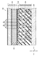
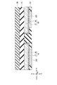
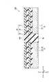
- FIG. 4 is a cross-sectional view of the electrode structure 100 according to the first embodiment.
- FIG. 4 is an enlarged cross-sectional view of the vicinity of the electrode structure 100 in FIG.
- the electrode structure 100 includes a plurality of pixel electrodes 10 and a plurality of dielectric layers 20.
- the plurality of pixel electrodes 10 are provided for each of the pixels Px.
- the plurality of pixel electrodes 10 are located in the pixel region Rp.
- the plurality of pixel electrodes 10 are separated from each other.
- a gap Sp is formed between the adjacent pixel electrodes 10.
- the gap Sp extends in the x direction and the y direction along each side of the pixel electrode 10 when viewed from the z direction.
- the plurality of pixel electrodes 10 are arranged in the x-direction and the y-direction with the gap Sp interposed therebetween.
- the plurality of pixel electrodes 10 have a plurality of electrode rows Er in the y direction in which the pixel electrodes 10 are arranged in the x direction with the gap Sp interposed therebetween.
- each electrode row Er in FIG. 2 the positions of the respective pixel electrodes 10 and the gap Sp in the x direction coincide with each other. That is, the pixel electrode 10 of the adjacent electrode row Er is located at the position of one pixel electrode 10 in the y direction, and the gap Sp of the adjacent electrode row Er is located at the position of one gap Sp in the y direction.
- the pixel electrode 10 shown in FIG. 2 is substantially rectangular in a plan view, and the length of one side is, for example, several ⁇ m.
- the width of the gap Sp is, for example, several hundred nm. The narrower the width of the gap Sp, the more preferable, but the processing becomes difficult.
- the pixel electrode 10 has, for example, a first conductive film 11 and a second conductive film 12.
- the first conductive film 11 is, for example, Ti or TiN.
- the first conductive film 11 is located between the plug wiring 222 and the second conductive film 12.
- the first conductive film 11 enhances the crystallinity of the second conductive film 12.
- the first conductive film 11 may be called a barrier metal.
- the thickness of the first conductive film 11 is preferably 20 nm or more. When the first conductive film 11 has a sufficient thickness, the crystallinity of the second conductive film 12 is improved.
- the crystallinity of the first conductive film 11 is good, the crystallinity of the second conductive film 12 is enhanced even if the thickness of the first conductive film 11 is less than 20 nm.
- the crystallinity of the first conductive film 11 can be enhanced by forming the first conductive film 11 by a film forming method such as an ion metal plasma method or a long throw method.
- the second conductive film 12 is, for example, an Al metal or an Al alloy, and as a specific example, an AlCu alloy.
- the thickness of the second conductive film 12 is, for example, 70 nm or more.
- the ends of the first conductive film 11 and the second conductive film 12 in the x-direction and the y-direction may be inclined with respect to the z-direction.
- the plurality of dielectric layers 20 include, for example, a first dielectric layer 21, a second dielectric layer 22, and a third dielectric layer 23.
- the first dielectric layer 21 extends over the plurality of pixel electrodes 10 in the xy plane and is also present in the gap Sp between the pixel electrodes 10.
- the first dielectric layer 21 has, for example, a refractive index of visible light of 1.45 or less, and is, for example, silicon oxide (SiO 2 ) or aluminum oxide (Al 2 O 3 ).
- the second dielectric layer 22 sandwiches the first dielectric layer 21 together with the plurality of pixel electrodes 10.
- the second dielectric layer 22 has a slit 22A at a position overlapping the gap Sp between the plurality of pixel electrodes 10 when viewed from the z direction.
- the slit 22A extends in the x direction and the y direction along each side of the pixel electrode 10 when viewed from the z direction.
- the second dielectric layer 22 is composed of, for example, a plurality of dielectric layers separated by slits 22A.
- the width of the slit 22A is, for example, several hundred nm. The width of the slit 22A may be changed, for example, depending on the wavelength of the incident light.
- the widths of the slits 22A in the respective liquid crystal display devices 200R, 200G, and 200B may be different.
- the side surface of the second dielectric layer 22 forming the slit 22A may be inclined with respect to the z direction.
- the second dielectric layer 22 contains a dielectric material having a higher refractive index than the first dielectric layer 21.
- the second dielectric layer 22 can be made of a dielectric material having a higher refractive index than the first dielectric layer 21.
- the difference in refractive index between the second dielectric layer 22 and the first dielectric layer 21 is preferably 0.45 or more, for example.
- the second dielectric layer 22, for example, has a refractive index of visible light larger than 1.45, such as silicon nitride (SiN), tantalum pentoxide (Ta 2 O 5 ), hafnium oxide (HfO 2 ), and niobium oxide (NbO).
- the reflectance at the interface between the second dielectric layer 22 and the first dielectric layer 21 is added to improve the reflectance of the electrode structure 100.
- the third dielectric layer 23 is in contact with the side surface 22s of the second dielectric layer 22 facing the slit 22A.
- the third dielectric layer 23 fills at least a part of the slit 22A.
- the third dielectric layer 23 is embedded in, for example, the slit 22A.
- the third dielectric layer 23 contains a dielectric material having a lower refractive index than the second dielectric layer 22.
- the third dielectric layer 23 can be made of a dielectric material having a lower refractive index than the second dielectric layer 22.
- the third dielectric layer 23 has, for example, a refractive index of visible light of 1.45 or less, and is, for example, silicon oxide (SiO 2 ) or aluminum oxide (Al 2 O 3 ).
- the third dielectric layer 23 is made of, for example, the same material as the first dielectric layer 21.
- the third dielectric layer 23 and the first dielectric layer 21 are made of the same material, it is difficult to confirm a clear interface between the first dielectric layer 21 and the third dielectric layer.
- the thickness of the first dielectric layer 21, the second dielectric layer 22, and the third dielectric layer 23 is designed according to the wavelength of the incident light.
- the thicknesses of the first dielectric layer 21, the second dielectric layer 22 and the third dielectric layer 23 in the respective liquid crystal display devices 200R, 200G and 200B are , Each may be different.
- the first manufacturing method includes a step of forming a conductive layer, a first dielectric layer, and a second dielectric layer containing a dielectric material having a higher refractive index than the first dielectric layer in order, and a conductive layer. It includes a step of forming a through hole penetrating at least the second dielectric layer of the first dielectric layer and the second dielectric layer, and a step of filling the through hole with the third dielectric layer.
- the conductive layer 91, the conductive layer 92, the dielectric layer 93, and the dielectric layer 94 are formed in this order.
- the dielectric layer 93 is an example of the first dielectric layer
- the dielectric layer 94 is an example of the second dielectric layer.
- Each layer is laminated by, for example, a sputtering method.
- the conductive layer 91 is a layer that becomes the first conductive film 11 of the pixel electrode 10.
- the conductive layer 92 is a layer that becomes the second conductive film 12 of the pixel electrode 10.
- the dielectric layer 93 is a layer that becomes a part of the first dielectric layer 21.
- the dielectric layer 94 is a layer to be the second dielectric layer 22.
- the materials and film thicknesses constituting each of the conductive layer 91, the conductive layer 92, the dielectric layer 93, and the dielectric layer 94 are appropriately selected according to the above-mentioned post-production configuration.
- a resist 95 having a predetermined pattern is formed on a part of the dielectric layer 94.
- An antireflection film (BARC) may be formed between the resist 95 and the dielectric layer 94.
- BARC antireflection film
- the conductive layer 91, the conductive layer 92, the dielectric layer 93, and the dielectric layer 94 are processed, and the holes H extending over the conductive layer 91, the conductive layer 92, the dielectric layer 93, and the dielectric layer 94.
- the mask used for processing uses a resist and is patterned by a method such as photolithography. At this time, the light-shielding mask used in the lithography process is, for example, a binary mask or a halftone mask.
- the dielectric layer and the conductive layer which are the work pieces, are processed by using an anisotropic dry etching method.
- the conductive layers 91 and 92 become pixel electrodes 10 by this processing
- the dielectric layer 94 becomes a second dielectric layer 22 by processing.
- a part of the hole H is a gap Sp between the pixel electrodes 10 and is a slit 22A of the second dielectric layer 22.
- BARC antireflection film
- the gap Sp between the pixel electrodes 10 can be narrowed.
- a dielectric layer 96 is formed to fill the hole H.
- the dielectric layer 96 is formed using, for example, high density plasma (HDP).
- the dielectric layer 96 is made of a dielectric layer material having a refractive index lower than that of the second dielectric layer 22.
- a part of the dielectric layer 96 constitutes a part of the first dielectric layer 21 and a third dielectric layer 23.
- the first dielectric layer 21 and the third dielectric layer 23 are formed at the same time, and these are integrated.
- the portion of the dielectric layer 96 located in the + z direction from the second dielectric layer 22 is removed.
- the dielectric layer 96 is removed, for example, by using chemical mechanical polishing (CMP).
- CMP chemical mechanical polishing
- the processing selection ratio of SiO 2 is set higher than the processing selection ratio of SiN as a condition for performing CMP.
- silica slurry and ceria slurry are used as the slurry.
- the second dielectric layer 22 functions as a stopper film for CMP.
- One surface of the third dielectric layer 23 in the + z direction may be recessed from one surface of the second dielectric layer 22 in the + z direction.
- the electrode structure 100 is obtained by removing a part of the dielectric layer 96.
- the second manufacturing method is different in that the sacrificial layer 81 is further formed on the surface of the dielectric layer 94 opposite to the dielectric layer 93 in the film forming step in the first manufacturing method.
- the conductive layer 91, the conductive layer 92, the dielectric layer 93, the dielectric layer 94, and the sacrificial layer 81 are formed in this order.
- the sacrificial membrane 81 is removed during the manufacturing process.
- the sacrificial layer 81 contains, for example, the same material as the third dielectric layer 23.
- the sacrificial layer 81 is, for example, silicon oxide.
- the sacrificial layer 81 can be removed by etching, for example.
- a resist 95 having a predetermined pattern is formed on a part of the dielectric layer 94.
- the hole H1 extending over the conductive layer 91, the conductive layer 92, the dielectric layer 93, the dielectric layer 94, and the sacrificial layer 81 is formed using the resist 95 as a mask.
- the conductive layers 91 and 92 become pixel electrodes 10 by this processing, and the dielectric layer 94 becomes a second dielectric layer 22 by processing.
- the hole H1 shrinks in diameter as it approaches the pixel electrode 10, for example.
- the width w1 of the hole H1 at the surface position of the sacrificial layer 81 in the + z direction is wider than the width w2 of the hole H1 at the surface position of the second dielectric layer 22 in the + z direction.
- the width w2 of the hole H1 at the surface position of the second dielectric layer 22 in the + z direction is wider than the width w3 of the hole H1 at the surface position of the pixel electrode 10 in the + z direction.
- the width w3 of the hole H1 at the surface position of the pixel electrode 10 in the + z direction is the maximum width of the gap Sp between the pixel electrodes 10.
- the sacrificial layer 81 and the resist 95 are removed, and the gap Sp is filled with the third dielectric layer 23 to form the electrode structure 100.
- the third manufacturing method includes a step of forming a conductive layer and a first dielectric layer in order, a step of forming through holes in the conductive layer and the first dielectric layer to form a pixel electrode, and a step between the pixel electrodes.
- a step of filling the second dielectric layer with a dielectric a step of laminating a second dielectric layer containing a dielectric material having a higher refractive electrode than the first dielectric layer over the first dielectric layer, and an opening in the second dielectric layer. It has a step of forming and a step of filling the opening with a third dielectric layer.
- the conductive layer 91, the conductive layer 92, and the dielectric layer 93 are formed in this order. It differs from the first manufacturing method shown in FIG. 5 in that the dielectric layer 94 is not laminated.
- a resist 95 having a predetermined pattern is formed on a part of the dielectric layer 93.
- the hole H2 extending over the conductive layer 91, the conductive layer 92, and the dielectric layer 93 is formed using the resist 95 as a mask.
- the conductive layers 91 and 92 become pixel electrodes 10 by this processing.
- a dielectric layer 96 is formed to fill the hole H2. A part of the dielectric layer 96 becomes a part of the first dielectric layer 21. Then, the portion of the dielectric layer 96 located in the + z direction from the first dielectric layer 21 is removed. The dielectric layer 96 is removed, for example, by using chemical mechanical polishing (CMP). First, the pixel electrode 10 and the first dielectric layer 21 of the electrode structure 100 are formed by CMP polishing.
- CMP chemical mechanical polishing
- the dielectric layer 94 is laminated on one surface of the first dielectric layer 21, and a resist 95 having a predetermined pattern is formed on a part of the dielectric layer 94.
- the dielectric layer 94 is processed using the resist 95 as a mask.
- the dielectric layer 94 becomes a second dielectric layer 22 by processing.
- the dielectric layer 82 is laminated over the second dielectric layer 22.
- the dielectric layer 82 is made of a dielectric layer material having a refractive index lower than that of the second dielectric layer 22.
- the dielectric layer 82 is made of, for example, the same material as the third dielectric layer 23.
- the portion of the dielectric layer 82 located in the + z direction from the second dielectric layer 22 is removed.
- the electrode structure 100 is formed by removing a part of the dielectric layer 82.
- the dielectric layer 82 is removed, for example, by using chemical mechanical polishing (CMP). If the dielectric layer 82 is treated as the third dielectric layer 23 without removing a part of the dielectric layer 82, the electrode structure 100A described later is obtained.
- CMP chemical mechanical polishing
- the fourth manufacturing method includes a step of laminating the conductive layer and the sacrificial layer, a step of forming through holes in the conductive layer and the sacrificial layer and filling the through holes with a dielectric, and a step of removing the sacrificial layer to remove the first dielectric. It includes a step of laminating the body layer and the second dielectric layer, a step of forming an opening in the second dielectric layer, and a step of filling the opening with the third dielectric layer.
- FIG. 15 is a diagram showing the middle of the fourth manufacturing method.
- the fourth manufacturing method is the same as the steps shown in FIGS. 10 to 12 of the third manufacturing method, except that the sacrificial layer 81 is used instead of the dielectric layer 93.
- the portion of the dielectric layer 96 located in the + z direction from the sacrificial layer 81 is removed.
- the dielectric layer 96 is removed, for example, by using chemical mechanical polishing (CMP). After that, by removing the sacrificial layer 81, the pixel electrode 10 is exposed as shown in FIG.
- the dielectric layer 93 and the dielectric layer 94 are laminated in order over the remaining dielectric layer 96 and the pixel electrode 10.
- the dielectric layer 93 and the dielectric layer 96 form the first dielectric layer 21.
- a resist 95 having a predetermined pattern is formed on a part of the dielectric layer 94.
- the dielectric layer 94 becomes the second dielectric layer 22.
- the electrode structure 100 is formed by filling the opening with the third dielectric layer 23.
- the fifth manufacturing method includes a step of forming through holes in the conductive layer to form pixel electrodes, a step of filling the space between the pixel electrodes with a dielectric, and a refractive index higher than that of the first dielectric layer and the first dielectric layer. It includes a step of laminating a second dielectric layer containing a high dielectric material over the pixel electrodes, a step of forming an opening in the second dielectric layer, and a step of filling the opening with the third dielectric layer.
- the fifth manufacturing method is the same as the third manufacturing method from the steps shown in FIGS. 10 to 12.
- the portion of the dielectric layer 96 located in the + z direction from the first dielectric layer 21 was removed, but in the fifth manufacturing method, the dielectric layer 96 and the first dielectric layer 21 were removed. Is removed to expose the pixel electrode 10.
- the process after exposing the pixel electrode 10 is the same as the fourth manufacturing method.
- the dielectric layer 93 and the dielectric layer 94 are laminated in this order over the remaining dielectric layer 96 and the pixel electrode 10.
- the dielectric layer 93 and the dielectric layer 96 form the first dielectric layer 21.
- a resist 95 having a predetermined pattern is formed on a part of the dielectric layer 94.
- the dielectric layer 94 becomes the second dielectric layer 22.
- the electrode structure 100 is formed by filling the opening with the third dielectric layer 23.
- the sixth manufacturing method includes a step of forming an insulating layer and forming a recess in the insulating layer, a step of filling the recess with a conductor, and a first dielectric layer and a second dielectric layer on the insulating layer and the conductor. It includes a step of laminating the dielectric layers in order, a step of forming a slit in the second dielectric layer, and a step of filling the slit with the third dielectric layer.
- the insulating layer 97 on which the plug wiring 222 is formed is formed, and the recess 97A is formed in a part of the insulating layer 97.
- a part of the insulating layer 97 becomes a part of the insulating layer 223 of the pixel circuit 220 (see FIG. 3).
- the recess 97A is formed by forming a resist 98 having a predetermined pattern on a part of the insulating layer 97 and processing the resist 98 as a mask.
- the recess 97A is formed by, for example, photolithography.
- the resist 98 is peeled off.
- two conductive layers are laminated on one surface of the insulating layer 97 and the plug wiring 222.
- the conductive layer is formed along the surfaces of the insulating layer 97 and the plug wiring 222.
- the laminated conductive layer is removed until a part of the insulating layer 97 is exposed.
- the conductive layer is processed by, for example, CMP.
- the two conductive layers are the first conductive film 16 and the second conductive film 17, respectively.
- the first conductive film 16 and the second conductive film 17 form the pixel electrode 15.
- the pixel electrode 15 is the same as the pixel electrode 10 shown in FIG. 4, except for the shapes of the first conductive film 16 and the second conductive film 17.
- the first dielectric layer 21 and the dielectric layer 99 are laminated in this order on a part of the pixel electrode 15 and the insulating layer 97.
- a slit 99A is provided in a part of the dielectric layer 99, and the slit 99A is filled with the third dielectric layer 23.
- a slit 99A is formed in the dielectric layer 99 to form a second dielectric layer 22.
- the first dielectric layer 21 and the third dielectric layer 23 are formed separately.
- the electrode structure 100 can be manufactured according to the first to sixth manufacturing methods.
- the method for manufacturing the electrode structure 100 is not limited to the above example.
- FIG. 21 is a cross-sectional view for explaining the operation of the electrode structure 100 according to the first embodiment.
- the lights L1A and L1B are incident on the electrode structure 100 from the + z direction to the ⁇ z direction.
- the light L1A incident on the position where it overlaps the pixel electrode 10 in the z direction will be described.
- the light L1A is reflected on the surface of the second dielectric layer 22, the interface between the first dielectric layer 21 and the second dielectric layer 22, and the surface of the pixel electrode 10. Since the pixel electrode 10 hardly transmits light, a large amount of light is reflected. That is, the utilization efficiency of the light L1A in the electrode structure 100 is high.
- the electrode structure 100 has a slit 22A in the second dielectric layer 22.
- the slit 22A is filled with, for example, the third dielectric layer 23.
- the medium inside the slit 22A (third dielectric layer 23) and the medium inside the second dielectric layer 22 are different.
- the light L1B diffracts after passing through the slit 22A. Due to diffraction, a part of the light L1B is directed toward the pixel electrode 10 side as the diffracted light L2.
- a part of the light L1B is diffracted into the diffracted light L2, so that the light L3 toward the gap Sp between the pixel electrodes 10 is suppressed.
- the diffracted light L2 is reflected on the surface of the pixel electrode 10 to become light L4.
- the light L3 goes to the pixel circuit 220 (see FIG. 3) through the gap Sp.
- the light L3 does not return to the liquid crystal layer 233 side.
- the electrode structure 100 according to the first embodiment can improve the reflectance and the light utilization efficiency.
- FIG. 22 is a cross-sectional view of the electrode structure 100A according to the first modification.
- the electrode structure 100A shown in FIG. 22 is different from the electrode structure 100 in that the third dielectric layer 23 extends over the second dielectric layer 22 and partially fills the slits 22A without filling all of them. different.
- the same components as those of the electrode structure 100 are designated by the same reference numerals and the description thereof will be omitted.
- the third dielectric layer 23 is formed along the surface of the second dielectric layer 22.
- the surface of the third dielectric layer 23 reflects the shape of the surface of the second dielectric layer 22 on which the slit 22A is formed.
- the third dielectric layer 23 has an opening 23A at a portion overlapping the slit 22A.
- the third dielectric layer 23 has a lower refractive index than the second dielectric layer 22.
- the third dielectric layer 23 may be, for example, an inorganic alignment film such as silicon oxide.
- the medium inside the slit 22A (third dielectric layer 23) and the medium inside the second dielectric layer 22 are different. Further, the medium inside the opening 23A and the medium inside the third dielectric layer 23 are different. Therefore, the light that has passed through the opening 23A and the slit 22A is diffracted. Therefore, even in the electrode structure 100A according to the first modification, the reflectance can be improved and the light utilization efficiency can be improved.
- FIG. 23 is a cross-sectional view of the electrode structure 100B according to the second modification.
- the electrode structure 100B shown in FIG. 23 is different from the electrode structure 100A according to the first modification in that the slit 22A is completely filled.
- the same components as those of the electrode structure 100A are designated by the same reference numerals and the description thereof will be omitted.
- the third dielectric layer 23 is formed over the second dielectric layer 22.
- the third dielectric layer 23 fills the slit 22A.
- the third dielectric layer 23 has a lower refractive index than the second dielectric layer 22.
- the third dielectric layer 23 may be, for example, an inorganic alignment film such as polyimide.
- the resin composition such as polyimide is viscous before curing, and the slit 22A is filled.
- the medium inside the slit 22A (third dielectric layer 23) and the medium inside the second dielectric layer 22 are different. Therefore, even in the electrode structure 100B according to the second modification, the reflectance can be improved and the light utilization efficiency can be improved.
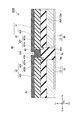
- FIG. 24 is a cross-sectional view of the electrode structure 101 according to the second embodiment.
- the electrode structure 101 according to the second embodiment is different from the electrode structure 100 according to the first embodiment in that it further has a fourth dielectric layer 24.
- Other configurations are the same, and the same configurations are designated by the same reference numerals and description thereof will be omitted.
- the fourth dielectric layer 24 extends over the first surfaces 22a and 23a of the second dielectric layer 22 and the third dielectric layer 23 on the side far from the first dielectric layer 21.
- the fourth dielectric layer 24 is made of, for example, a dielectric material having a higher refractive index than the second dielectric layer 22.
- the fourth dielectric layer 24 includes, for example, silicon nitride (SiN), tantalum pentoxide (Ta 2 O 5 ), hafnium oxide (HfO 2 ), niobium oxide (NbO, NbO 2 , Nb 2 O 3 , Nb 2 O 5). ), Titanium oxide (TiO 2 ).
- the difference in refractive index between the fourth dielectric layer 24 and the first dielectric layer 21 is preferably 0.70 or more, for example.
- the second dielectric layer 22 has a slit 22A.
- the electrode structure 101 can suppress the difference in reflection intensity for each wavelength.
- the diffraction angle of the diffracted light L2' is different for each wavelength. For example, light having a large wavelength has a larger diffraction angle than light having a small wavelength.
- the intensity of red light may be increased at a position tilted by a certain angle from the z direction, and the intensity of blue light may be increased at a position tilted by a different angle.
- the difference in the reflection angle for each wavelength can cause color unevenness in the output image.
- the electrode structure 101 has a fourth dielectric layer 24 containing a dielectric material having a higher refractive index than the second dielectric layer 22.
- the light L1B is reflected on the surface of the fourth dielectric layer 24 and at the interface between the fourth dielectric layer 24 and the third dielectric layer 23 before reaching the diffraction point. That is, when the fourth dielectric layer 24 is provided, the reflection interface on which the light L1B is reflected increases. When the reflection interface increases, the amount of light reaching the diffraction point decreases, and the intensity of the diffracted light L2'decreases. As the ratio of the diffracted light L2'decreases, the ratio of the light L4'in the entire reflected light reflected from the entire electrode structure 101 decreases.
- the light L4' has a difference in intensity for each wavelength and is a cause of color unevenness. By reducing the ratio of light L4'in the reflected light, it is possible to suppress the difference in reflection intensity for each wavelength.
- the decrease in the intensity of the diffracted light L2' is due to the decrease in the amount of light reaching the diffraction point, and does not mean that the ratio of the diffracted light L2'and the light L3' has changed. That is, even if the intensity of the diffracted light L2'decreases, the intensity of the light L3' does not increase. Therefore, the light utilization efficiency of the electrode structure 101 does not decrease.
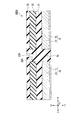
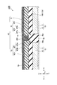
- FIG. 25 is a cross-sectional view of the electrode structure 102 according to the third embodiment.
- the electrode structure 102 according to the third embodiment has a plurality of dielectric layers 30 different from the electrode structure 100 according to the first embodiment.
- Other configurations are the same, and the same configurations are designated by the same reference numerals and description thereof will be omitted.
- the electrode structure 102 has a pixel electrode 10 and a plurality of dielectric layers 30.
- the plurality of dielectric layers 30 have a plurality of first dielectric layers 31, a plurality of second dielectric layers 32, and a plurality of third dielectric layers 33.
- the first dielectric layer 31 extends in the xy plane.
- the second dielectric layer 32 has a slit 32A and spreads in the xy plane.
- the first dielectric layer 31 and the second dielectric layer 32 are alternately laminated in the z direction.
- the third dielectric layer 33 fills the slit 32A of the second dielectric layer 32, respectively.
- the materials, refractive indexes, etc. of the first dielectric layer 31, the second dielectric layer 32, and the third dielectric layer 33 are the first dielectric layer 21, the second dielectric layer 22, and the second dielectric layer 22 according to the first embodiment. This is the same as for each of the third dielectric layers 23.
- the second dielectric layer 32 has a slit 32A.
- the slit 32A diffracts a part of the light incident on the pixel electrode 10 at a position that does not overlap in the z direction (a position that overlaps with the gap Sp). Therefore, the electrode structure 102 can improve the reflectance as in the electrode structure 100 according to the first embodiment.
- the electrode structure 102 has a plurality of slits 32A at different height positions in the z direction. The light is diffracted after passing through the slit 32A.
- the electrode structure 102 according to the third embodiment has more diffraction points than the electrode structure 100 according to the first embodiment. Therefore, the electrode structure 102 can further suppress the incident light toward the gap Sp between the pixel electrodes 10, and can further improve the light utilization efficiency.
- FIG. 26 is a cross-sectional view of the electrode structure 102A according to the third modification.
- the electrode structure 102A shown in FIG. 26 is different from the electrode structure 102 in that it has a fourth dielectric layer 34 over the second dielectric layer 32.
- the electrode structure 102A is a combination of the features of the electrode structure 101 according to the second embodiment and the features of the electrode structure 102 according to the third embodiment.
- the fourth dielectric layer 34 is formed over the second dielectric layer 32 located at the most + z direction among the plurality of second dielectric layers 32.
- the fourth dielectric layer 34 is the same as the fourth dielectric layer 24 according to the second embodiment.
- the fourth dielectric layer 34 is not limited to the example shown in FIG. 26, and may be formed over the other second dielectric layer 32 among the plurality of second dielectric layers 32. That is, at the position where it overlaps with the electrode structure 10, the first dielectric layer 31, the second dielectric layer 32, the fourth dielectric layer 34, the first dielectric layer 31, and the second dielectric layer 32 are laminated in this order. You may.
- the electrode structure 102A has a plurality of slits 32A at different height positions in the z direction. The light is diffracted after passing through the slit 32A. Therefore, the electrode structure 102A can further suppress the incident light toward the gap Sp between the pixel electrodes 10, and can further improve the light utilization efficiency.
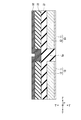
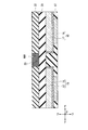
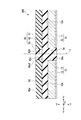
- FIG. 27 is a cross-sectional view of the electrode structure 103 according to the fourth embodiment.
- the electrode structure 103 according to the fourth embodiment has a plurality of dielectric layers 40 different from the electrode structure 100 according to the first embodiment.
- Other configurations are the same, and the same configurations are designated by the same reference numerals and description thereof will be omitted.
- the electrode structure 103 has a pixel electrode 10 and a plurality of dielectric layers 40.
- the plurality of dielectric layers 40 include a first dielectric layer 41, a second dielectric layer 42, and a third dielectric layer 43.
- the first dielectric layer 41 spreads in the xy plane.
- the first dielectric layer 41 has a recess 41a at a position where it overlaps the gap Sp in the z direction.
- the recess 41a is recessed in the ⁇ z direction from the boundary surface Bs along the boundary between the first dielectric layer 41 and the second dielectric layer 42.
- the second dielectric layer 42 has a main body portion 42X that overlaps with the pixel electrode 10 when viewed from the z direction, and a protruding portion 42Y.
- the protruding portion 42Y is located on the side surface side of the second dielectric layer 42 facing the slit 42A of the main body portion 42X.
- the protruding portion 42Y is a portion that protrudes toward the slit 42A with respect to the side surface 10a of the pixel electrode 10 facing the gap Sp when viewed from the z direction.
- the protruding portion 42Y protrudes from the side surface 10a of the pixel electrode 10 in the x direction or the y direction in a plan view from the z direction.
- the protruding portion 42Y has a protruding main body portion 42Ya and an extending portion 42Yb.
- the protruding main body portion 42Ya is at the same height position as the main body portion 42X in the z direction.
- the extending portion 42Yb projects in the ⁇ z direction from the interface Bs between the first dielectric layer 41 and the second dielectric layer 42.
- the extending portion 42Yb is arranged in the recess 41a of the first dielectric layer 41.
- the lower end of the extending portion 42Yb is located at a position in the + z direction from the surface 10A (12a) of the pixel electrode 10.
- the third dielectric layer 43 fills the slit 42A of the second dielectric layer 42.
- the materials, refractive indexes, etc. of the first dielectric layer 41, the second dielectric layer 42, and the third dielectric layer 43 are the first dielectric layer 21, the second dielectric layer 22, and the second dielectric layer 22 according to the first embodiment. This is the same as for each of the third dielectric layers 23.
- the third dielectric layer 43 may be, for example, an inorganic alignment film such as silicon oxide, an organic alignment film such as polyimide, or the like.
- the second dielectric layer 42 has a slit 42A.
- the slit 42A diffracts a part of the light incident on the pixel electrode 10 at a position that does not overlap in the z direction (a position that overlaps with the gap Sp). Therefore, the electrode structure 103 can improve the reflectance as in the electrode structure 100 according to the first embodiment.
- the electrode structure 103 has a protruding portion 42Y.
- the protrusion 42Y increases diffraction.
- the protruding portion 42Y has an extending portion 42Yb.
- the extending portion 42Yb also increases diffraction. Therefore, the electrode structure 103 can further suppress the incident light toward the gap Sp between the pixel electrodes 10, and can further improve the light utilization efficiency.
- FIG. 28 is a cross-sectional view of the electrode structure 103A according to the fourth modification.
- the electrode structure 103A shown in FIG. 28 is different from the electrode structure 103 in that the third dielectric layer 43 extends over the second dielectric layer 42.
- the same components as those of the electrode structure 103 are designated by the same reference numerals and the description thereof will be omitted.
- the third dielectric layer 43 is formed along the surface of the second dielectric layer 42.
- the surface of the third dielectric layer 43 reflects the shape of the surface of the second dielectric layer 42 in which the slit 42A is formed.
- the third dielectric layer 43 has an opening 43A at a portion overlapping the slit 42A.
- the electrode structure 103A has the same effect as the electrode structure 103 and can improve the reflectance.
- the electrode structure 103A is a combination of the features of the electrode structure 103 according to the fourth embodiment and the features of the electrode structure 100A according to the first modification.
- FIG. 29 is a cross-sectional view of the electrode structure 103B according to the fifth modification.
- the electrode structure 103B shown in FIG. 29 is different from the electrode structure 103A according to the fifth modification in that the third dielectric layer 43 does not have an opening 43A.
- the same components as those of the electrode structure 103A are designated by the same reference numerals and the description thereof will be omitted.
- the third dielectric layer 43 is formed over the second dielectric layer 42.
- the surface of the third dielectric layer 43 in the + z direction is flattened regardless of the shape of the surface of the second dielectric layer 42 in which the slit 42A is formed.
- the fourth dielectric layer 43 may be, for example, an inorganic alignment film such as polyimide.
- the resin composition such as polyimide is viscous before curing, and the opening 43A is filled.
- the electrode structure 103B has the same effect as the electrode structure 103, and can improve the reflectance.
- the electrode structure 103B is a combination of the features of the electrode structure 103 according to the fourth embodiment and the features of the electrode structure 100B according to the second modification.
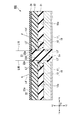
- FIG. 30 is a cross-sectional view of the electrode structure 104 according to the fifth embodiment.
- the electrode structure 104 according to the fifth embodiment has a plurality of dielectric layers 50 different from the electrode structure 100 according to the first embodiment.
- Other configurations are the same, and the same configurations are designated by the same reference numerals and description thereof will be omitted.
- the electrode structure 104 has a pixel electrode 10 and a plurality of dielectric layers 50.
- the plurality of dielectric layers 50 include a first dielectric layer 51, a second dielectric layer 52, a third dielectric layer 53, and a fifth dielectric layer 55.
- the first dielectric layer 51 spreads in the xy plane.
- the second dielectric layer 52 has a slit 52A and spreads in the xy plane.
- the third dielectric layer 53 is in contact with the side surface 52s of the second dielectric layer 52 in which the slit 52A is formed.
- the third dielectric layer 53 fills, for example, a part of the slit 52A.
- the materials, refractive indexes, etc. of the first dielectric layer 51, the second dielectric layer 52, and the third dielectric layer 53 are the first dielectric layer 21, the second dielectric layer 22, and the second dielectric layer 22 according to the first embodiment. This is the same as for each of the third dielectric layers 23.
- the fifth dielectric layer 55 is in contact with the inner surface 53s of the third dielectric layer 53.
- the fifth dielectric layer 55 fills, for example, a part of the slit 52A.
- the fifth dielectric layer 55 has a higher refractive index than the third dielectric layer 53.
- the same material as the second dielectric layer 52 can be used, and the fifth dielectric layer 55 may be made of the same material as the second dielectric layer 52.
- the second dielectric layer 52 has a slit 52A.
- the slit 52A diffracts a part of the light incident on the pixel electrode 10 at a position that does not overlap with the pixel electrode 10 in the z direction (a position that overlaps with the gap Sp). Therefore, the electrode structure 104 can improve the reflectance as in the electrode structure 100 according to the first embodiment.
- the electrode structure 104 has a fifth dielectric layer 55 having a higher refractive index than the third dielectric layer 53 inside the third dielectric layer 53.
- the electrode structure 104 can further suppress the incident light toward the gap Sp between the pixel electrodes 10, and can further improve the light utilization efficiency.
- the configuration in which the slit 52A is filled with the third dielectric layer 53 and the fifth dielectric layer 55 has been described as an example, but the slit 52A may be filled with more plurality of dielectric layers.
- the medium having a low refractive index and the medium having a high refractive index are alternately arranged from a position close to the second dielectric layer 52 when viewed from the z direction.
- FIG. 31 is a cross-sectional view of the electrode structure 104A according to the fifth modification.
- the third dielectric layer 53 extends over the second dielectric layer 52, and the opening 53A of the third dielectric layer 53 is filled with the fifth dielectric layer 55.
- the same components as those of the electrode structure 104 are designated by the same reference numerals and the description thereof will be omitted.
- the third dielectric layer 53 is formed along the surface of the second dielectric layer 52.
- the surface of the third dielectric layer 53 reflects the shape of the surface of the second dielectric layer 52 on which the slit 52A is formed.
- the third dielectric layer 53 has an opening 53A at a portion overlapping the slit 52A.
- the fifth dielectric layer 55 fills the opening 53A.
- the electrode structure 104A has the same effect as the electrode structure 104, and can improve the reflectance.
- the electrode structure 104A is a combination of the features of the electrode structure 104 according to the fifth embodiment and the features of the electrode structure 100A according to the first modification.
- FIG. 32 is a cross-sectional view of the electrode structure 105 according to the sixth embodiment.
- the electrode structure 105 according to the sixth embodiment has a different shape of the side surface 62s of the second dielectric layer 62 from the electrode structure 100 according to the first embodiment.
- Other configurations are the same, and the same configurations are designated by the same reference numerals and description thereof will be omitted.
- the electrode structure 105 has a pixel electrode 10 and a plurality of dielectric layers 60.
- the plurality of dielectric layers 60 include a first dielectric layer 61, a second dielectric layer 62, and a third dielectric layer 63.
- the first dielectric layer 61 spreads in the xy plane.
- the second dielectric layer 62 has a slit 62A and extends in the xy plane.
- the third dielectric layer 63 is in contact with the side surface 62s of the second dielectric layer 62 in which the slit 62A is formed.
- the materials, refractive indexes, etc. of the first dielectric layer 61, the second dielectric layer 62, and the third dielectric layer 63 are the first dielectric layer 21, the second dielectric layer 22, and the second dielectric layer 22 according to the first embodiment. This is the same as for each of the third dielectric layers 23.
- At least a part of the side surface 62s of the second dielectric layer 62 is inclined with respect to the z direction.
- the side surface 62s is inclined in a direction away from the center line C between the pixel electrodes 10 as the distance from the pixel electrodes 10 in the z direction increases.
- the width of the slit 62A in the x-direction and the y-direction becomes wider as the distance from the pixel electrode 10 increases.
- the boundary point 62s1 between the first surface 62a and the side surface 62s of the second dielectric layer 62 in the + z direction is located, for example, closer to the center line C than the side surface 10a of the pixel electrode 10 facing the gap Sp.
- the second dielectric layer 62 has a slit 62A.
- the slit 62A diffracts a part of the light incident on the pixel electrode 10 at a position that does not overlap with the pixel electrode 10 in the z direction (a position that overlaps with the gap Sp). Therefore, the electrode structure 105 can improve the reflectance as in the electrode structure 100 according to the first embodiment.
- the side surface 62s of the second dielectric layer 62 is inclined.
- the side surface 62s bends the light incident on the second dielectric layer 62 from the third dielectric layer 63 toward the pixel electrode 10.
- the proportion of light reflected by the pixel electrode 10 increases.
- the electrode structure 105 can further suppress the incident light toward the gap Sp between the pixel electrodes 10, and can further improve the light utilization efficiency.
- the sixth embodiment shows an example in which all the side surfaces 62s are inclined, a part of the side surface 62s may be inclined. Further, the inclination angle of the inclined surface with respect to the z direction is not limited to a constant case, and may change. For example, a part of the side surface 62 may be curved and have a curvature.
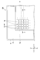
- FIG. 33 is a plan view of the liquid crystal display device 201 according to the seventh embodiment.
- the liquid crystal display device 201 according to the seventh embodiment has a different arrangement of pixels Px in the pixel region Rp1 from the liquid crystal display device 200 according to the first embodiment.
- Other configurations are the same, and the same configurations are designated by the same reference numerals and description thereof will be omitted.
- the liquid crystal display device 201 has a pixel region Rp1 and a peripheral region Re.
- the pixel region Rp1 is a region in which a plurality of pixels Px are formed.
- the pixel region Rp1 has a plurality of electrode rows Er in which the pixels Px are arranged in the x direction in the y direction.
- the peripheral region Re is a region surrounding the pixel region Rp1 in a plan view from the z direction.
- first electrode row Er1 An arbitrary electrode row among the plurality of electrode rows Er is referred to as a first electrode row Er1
- second electrode row Er2 an electrode row adjacent to the first electrode row Er1 in the y direction
- the pixels Px and the gap Sp are alternately arranged in the x direction.
- the pixel Px (pixel electrode 10) of the first electrode row Er1 is located at a position overlapping the gap Sp of the second electrode row Er2 in the y direction.
- the pixel Px (pixel electrode 10) of the second electrode row Er2 is located at a position overlapping the gap Sp of the first electrode row Er1 in the y direction.
- the positions of the pixels Px (pixel electrodes 10) in the x direction of the first electrode row Er1 and the second electrode row Er2 are deviated from each other.
- the plurality of pixels Px (pixel electrodes 10) are arranged in a zigzag manner in the y direction.
- the plurality of pixels Px (pixel electrodes 10) are arranged in a staggered arrangement, for example.
- the light incident on the gap Sp is not reflected, which causes a decrease in light utilization efficiency. Therefore, if the area occupied by the gap Sp in the pixel region Rp1 is small, the light utilization efficiency is improved.
- the corners of the plurality of pixels Px may be arcuate due to processing accuracy. For example, as shown in FIG. 2, when the positions of adjacent pixels Px in the x-direction and the y-direction match, the region surrounded by the four pixels Px causes a decrease in light utilization efficiency. This is because the distance between the pixels Px adjacent in the diagonal direction is larger than the distance between the pixels Px adjacent in the x direction or the y direction.
- the region surrounded by the four pixel Px becomes. Not formed. Therefore, the area occupied by the gap Sp in the pixel region Rp1 can be reduced, and the light utilization efficiency of the liquid crystal display device 201 can be improved.
- each pixel Px has, for example, the electrode structure 100 according to the first embodiment. Therefore, the liquid crystal display device 201 according to the seventh embodiment has the same effect as the electrode structure 100 according to the first embodiment.
- FIG. 34 is a plan view of the liquid crystal display device 201A according to the sixth modification.
- the liquid crystal display device 201A according to the sixth modification has a different shape of the pixel Px1 in the pixel region Rp2 from the liquid crystal display device 201 shown in FIG. 33.
- Other configurations are the same, and the same configurations are designated by the same reference numerals and description thereof will be omitted.
- Pixel Px1 is a hexagon when viewed from the z direction. Pixels Px1 are hexagonal close-packed when viewed from the z direction. By closely arranging the pixels Px1, the area occupied by the gap Sp in the pixel region Rp2 can be reduced. Therefore, the liquid crystal display device 201A according to the sixth modification is excellent in light utilization efficiency.
- the pixel Px has a rectangular or hexagonal shape has been described as an example, but the shape of the pixel Px is not limited to these.
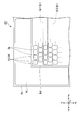
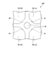
- FIG. 35 is a plan view of a main part of the liquid crystal display device 202 according to the eighth embodiment.
- the liquid crystal display device 202 according to the eighth embodiment is different from the liquid crystal display device 200 according to the first embodiment in that the corner electrode CE is provided in a region surrounded by four pixels Px (pixel electrodes 10).
- Other configurations are the same, and the same configurations are designated by the same reference numerals and description thereof will be omitted.
- the liquid crystal display device 202 has a pixel area and a peripheral area.
- FIG. 35 is an enlarged view of a part of the pixel area.
- the pixels Px are arranged in the x direction and the y direction.
- the corner electrode CE is provided, for example, in a region surrounded by the corners ed of the four pixels Px.
- the corner electrode CE is made of, for example, the same material as the pixel electrode 10.
- the corner electrode CE may have a reflection function.
- the corner electrode CE may be a floating electrode that is not connected to the pixel circuit 220 and has an independent potential. Further, the corner electrode CE may be connected to the ground to create a capacitance between the corner electrode CE and the pixel electrode.
- the area surrounded by the four pixels Px causes a decrease in light utilization efficiency.
- the corner electrode CE By providing the corner electrode CE in the region surrounded by the four pixels Px, the area ratio occupied by the gap in the pixel region can be reduced and the light utilization efficiency can be improved.
- each pixel Px has, for example, the electrode structure 100 according to the first embodiment. Therefore, the liquid crystal display device 202 according to the eighth embodiment has the same effect as the electrode structure 100 according to the first embodiment.
- the corner electrodes are located in the region surrounded by the three pixels Px. May be provided.
- FIG. 36 is a plan view of the liquid crystal display device 203 according to the ninth embodiment.
- the liquid crystal display device 203 according to the ninth embodiment has a peripheral region Re1 configuration different from that of the liquid crystal display device 200 according to the first embodiment.
- Other configurations are the same, and the same configurations are designated by the same reference numerals and description thereof will be omitted.
- the liquid crystal display device 203 has a pixel region Rp and a peripheral region Re1.
- the peripheral region Re1 has a plurality of peripheral electrodes PE1.
- the peripheral electrodes PE1 are aligned in the x direction and the y direction.
- the size (area) of each peripheral electrode PE1 is substantially the same as the size (area) of each pixel electrode 10.
- substantially the same means that blurring within 15% is allowed based on the area of the pixel electrode 10.
- a flattening process for flattening the surface may be performed.
- a step of removing a portion of the dielectric layer 96 in the first manufacturing method, the third manufacturing method, the fourth manufacturing method, and the fifth manufacturing method that is located in the + z direction from the second dielectric layer 22 (FIGS. 7 and 12). , See FIG. 15) is an example of a flattening process.
- the step of removing the laminated conductive layer in the sixth manufacturing method until a part of the insulating layer 97 is exposed is also an example of the flattening process.
- the flattening process is performed, for example, by CMP.
- the flattening process is often performed at once over the pixel region Rp and the peripheral region Re1. If the pattern density of the pixel Px in the pixel region Rp and the pattern density of the peripheral electrode PE1 in the peripheral region Re1 are different, the speed of the flattening process changes between the pixel region Rp and the peripheral region Re1. As a result, the flattening process in the pixel region Rp may not proceed with respect to the peripheral region Re1, or conversely, the electrode structure 100 in the pixel region Rp may be overpolished. Over-polishing causes peeling of the film of each laminated layer.
- the peripheral electrode PE1 in the peripheral region Re1 is patterned using photolithography or the like.
- the processing of the pixel electrode 10 in the pixel region Rp and the processing of the peripheral electrode PE1 in the peripheral region Re1 may be performed at the same time, or may be separated as separate steps.
- the peripheral region Re1 may have a connecting portion Cp between adjacent peripheral electrodes PE1 when viewed from the z direction.
- the connecting portion Cp is provided, for example, at a position extending over the corner portion of each of the four peripheral electrodes PE1.
- the connection portion Cp is not limited to this case as long as a plurality of peripheral electrodes PE1 can be electrically connected.
- the peripheral electrode PE1 is electrically connected to the common electrode 235. By electrically connecting each of the plurality of peripheral electrodes PE1 to each other, it is not necessary to provide the plug wiring 222 and the wiring 221 for each peripheral electrode PE1.
- each pixel Px has, for example, the electrode structure 100 according to the first embodiment. Therefore, the liquid crystal display device 203 according to the ninth embodiment has the same effect as the electrode structure 100 according to the first embodiment.
- the content of the present disclosure may have the following structure.
- a plurality of dielectric layers laminated in the first direction with respect to the plurality of pixel electrodes are provided.
- the plurality of dielectric layers are A first dielectric layer extending over the plurality of pixel electrodes in a direction intersecting the first direction, A position that contains a dielectric material having a higher refractive index than the first dielectric layer, sandwiches the first dielectric layer with the plurality of pixel electrodes, and overlaps with a gap between adjacent pixel electrodes when viewed from the first direction.
- the third dielectric layer has an opening, contains a dielectric material having a higher refractive index than the third dielectric layer, and further includes a fifth dielectric layer embedded in the opening.
- the plurality of dielectric layers include the first dielectric layer and the second dielectric layer.
- a fourth dielectric layer containing a dielectric material having a higher refractive index than the second dielectric layer and spreading over any second dielectric layer among the plurality of second dielectric layers is further provided.
- the second dielectric layer has a protrusion on the side surface of the second dielectric layer facing the slit, which protrudes toward the slit side with respect to the side surface of the pixel electrode facing the gap when viewed from the first direction.
- the electrode structure according to any one of (1) to (7) above.
- the plurality of pixel electrodes have a plurality of electrode rows in which pixel electrodes are arranged in a second direction intersecting the first direction.
- the plurality of electrode rows include a first electrode row and a second electrode row arranged alternately in a third direction orthogonal to the second direction.
- each of the plurality of pixel electrodes has a rectangular or hexagonal shape when viewed from the first direction.
- the pixel region on which the plurality of pixel electrodes are formed and A peripheral area surrounding the pixel area when viewed from the first direction is provided.
- the peripheral region has a plurality of peripheral electrodes and has a plurality of peripheral electrodes.
- a liquid crystal display device comprising an alignment film located between the liquid crystal layer and the electrode structure.
- a projection-type display device including the liquid crystal display device according to (15) and a light source that irradiates the liquid crystal display device with light from the common electrode toward the electrode structure.
- a method for producing an electrode structure comprising a step of filling the through hole with a third dielectric layer containing a dielectric material having a refractive index lower than that of the second dielectric layer.
- a sacrificial layer containing the same material as the third dielectric layer is further formed on the surface of the second dielectric layer opposite to the first dielectric layer.
- the step of forming a slit in the second dielectric layer and A method for producing an electrode structure comprising a step of filling the slit with a third dielectric layer containing a dielectric material having a refractive index lower than that of the second dielectric layer.
Landscapes
- Physics & Mathematics (AREA)
- Nonlinear Science (AREA)
- General Physics & Mathematics (AREA)
- Mathematical Physics (AREA)
- Chemical & Material Sciences (AREA)
- Crystallography & Structural Chemistry (AREA)
- Optics & Photonics (AREA)
- Geometry (AREA)
- Liquid Crystal (AREA)
- Spectroscopy & Molecular Physics (AREA)
- Engineering & Computer Science (AREA)
- Microelectronics & Electronic Packaging (AREA)
- Devices For Indicating Variable Information By Combining Individual Elements (AREA)
- Projection Apparatus (AREA)
- Laminated Bodies (AREA)
Abstract
この電極構造体は、互いに離間して配置する複数の画素電極と、前記複数の画素電極に対して第1方向に積層された複数の誘電体層と、を備え、前記複数の誘電体層は、前記第1方向と交差する方向に前記複数の画素電極に亘って広がる第1誘電体層と、前記第1誘電体層より屈折率が高い誘電体材料を含み、前記複数の画素電極と共に前記第1誘電体層を挟み込むとともに、前記第1方向から見て隣接する画素電極間の隙間と重なる位置にスリットを有する第2誘電体層と、を有する。
Description
本開示は、電極構造体、液晶表示装置、投射型表示装置及び電極構造体の製造方法に関する。
投射型表示装置に用いられる液晶表示装置には、光反射と液晶制御とを兼ねる画素電極を用いた反射型液晶表示装置が知られている。反射型液晶表示装置は、液晶の偏光を利用して入射した光の反射を画素電極によりオン・オフする。
反射型の液晶表示装置は、光の入射方向と反対側に配線等を設けることができ、透過型の液晶表示装置と比較して高解像度化に適していると言われている。また反射型の液晶表示装置は、透過型の液晶表示装置と比較して、偏光に必要な光路長を半分にでき、少ない駆動電圧で動作できる。
例えば、特許文献1には、反射型の液晶表示装置が記載されている。特許文献1には、光利用効率を高めるために、反射画素電極上に誘電体層の多層膜を設けることが記載されている。また反射型の液晶表示装置は、複数の画素電極を有する。複数の画素電極は、直上に位置する液晶をそれぞれ独立に制御するために、隙間を介して離間されている。複数の画素電極の間の隙間は、入射した光を反射できず、反射率の低下の原因となる。特許文献1では、複数の画素電極の間の隙間に、漏れ光を抑制するための遮光膜を設けている。
反射型の液晶表示装置の反射率は、出力画像の輝度に大きな影響を及ぼす。反射型の液晶表示装置の反射率が向上すると、出力画像の画質が向上する。このため、液晶表示装置に入射した光の利用効率の更なる向上が求められている。
本開示は上記事情に鑑みてなされたものであり、光の利用効率を向上させることができる電極構造体、液晶表示装置、投射型表示装置及び電極構造体の製造方法を提供する。
本開示の第1の態様に係る電極構造体は、互いに離間して配置する複数の画素電極と、前記複数の画素電極に対して第1方向に積層された複数の誘電体層と、を備え、前記複数の誘電体層は、前記第1方向と交差する方向に前記複数の画素電極に亘って広がる第1誘電体層と、前記第1誘電体層より屈折率が高い誘電体材料を含み、前記複数の画素電極と共に前記第1誘電体層を挟み込むとともに、前記第1方向から見て隣接する画素電極間の隙間と重なる位置にスリットを有する第2誘電体層と、を有する。
[作用]
電極構造体に向って入射した光の一部は、第2誘電体層のスリットを通過する。第2誘電体層のスリットを通過した光は、第1誘電体層に入射する際に、光の入射方向から見て第2誘電体層の裏面側に向って回り込む。すなわち、第2誘電体層のスリットを通過した光は、第1誘電体層との境界で回折する。第2誘電体層のスリットは、複数の画素電極の間の隙間と重なる位置にある。回折現象により上記隙間に至る光の量が減少する。
電極構造体に向って入射した光の一部は、第2誘電体層のスリットを通過する。第2誘電体層のスリットを通過した光は、第1誘電体層に入射する際に、光の入射方向から見て第2誘電体層の裏面側に向って回り込む。すなわち、第2誘電体層のスリットを通過した光は、第1誘電体層との境界で回折する。第2誘電体層のスリットは、複数の画素電極の間の隙間と重なる位置にある。回折現象により上記隙間に至る光の量が減少する。
以下、本実施形態について、図を適宜参照しながら詳細に説明する。以下の説明で用いる図面は、特徴をわかりやすくするために便宜上特徴となる部分を拡大して示している場合があり、各構成要素の寸法比率などは実際とは異なっていることがある。以下の説明において例示される材料、寸法等は一例であって、本開示はそれらに限定されるものではなく、本開示の効果を奏する範囲で適宜変更して実施することが可能である。
以下の説明では、適宜、x、y、zの直交座標系を用いて説明する。x方向は、後述する第2方向の一例である。y方向は、後述する第3方向の一例である。z方向は、後述する第1方向の一例である。各方向で+、-を付けて、一方の方向とその反対の方向を示している。
[第1実施形態]
「投射型表示装置」
図1は、第1実施形態にかかる投射型表示装置300の模式図である。投射型表示装置300は、画像信号に基づき、光源から出力された光(照明光)をRGBの色毎に変調して合成し、画像光を生成する。投射型表示装置300は、例えば、プロジェクタ、ヘッドアップディスプレイのスクリーン部に画像を投影するもの等に用いられる。図1に示す投射型表示装置300は、赤、青および緑の各色用の反射型の液晶表示装置200R、200G、200Bを3枚用いてカラー画像表示を行う、いわゆる3板方式の反射型プロジェクタである。以下、赤、青および緑の3色の3板方式の反射型プロジェクタを例に説明するが、赤、青および緑のうちの2色を1つの液晶表示装置で制御する2板方式の反射型プロジェクタでもよいし、フィールドシークエンシャル方式等を利用し3色を一つの液晶表示装置で制御する単板方式の反射型プロジェクタでもよい。
「投射型表示装置」
図1は、第1実施形態にかかる投射型表示装置300の模式図である。投射型表示装置300は、画像信号に基づき、光源から出力された光(照明光)をRGBの色毎に変調して合成し、画像光を生成する。投射型表示装置300は、例えば、プロジェクタ、ヘッドアップディスプレイのスクリーン部に画像を投影するもの等に用いられる。図1に示す投射型表示装置300は、赤、青および緑の各色用の反射型の液晶表示装置200R、200G、200Bを3枚用いてカラー画像表示を行う、いわゆる3板方式の反射型プロジェクタである。以下、赤、青および緑の3色の3板方式の反射型プロジェクタを例に説明するが、赤、青および緑のうちの2色を1つの液晶表示装置で制御する2板方式の反射型プロジェクタでもよいし、フィールドシークエンシャル方式等を利用し3色を一つの液晶表示装置で制御する単板方式の反射型プロジェクタでもよい。
投射型表示装置300は、例えば、光軸Lに沿って光源301とインテグレータ302とダイクロイックミラー303(波長選択素子)とを、光の進む順に備える。光源301は、例えば、赤色光R、青色光Bおよび緑色光Gを含んだ白色光を発する。光源301は、例えば、ハロゲンランプ、メタルハライドランプ、キセノンランプ等のランプ、半導体レーザ(LD)または発光ダイオード(LED)等の固体光源である。また光源301は、波長帯域ごとの光を別々に出射してもよい。インテグレータ302は、例えば、PSコンバータ等を含む。インテグレータ302は、光源301からの光を均一化し、光の利用効率を高める。ダイクロイックミラー303は、例えば白色光を赤色光R、青色光Bおよび緑色光Gに分離する。
投射型表示装置300は、赤色光Rおよび緑色光Gの光路上において、偏光ビームスプリッタ304と集光レンズ306とダイクロイックミラー308とを、光の進む順に有する。また投射型表示装置300は、青色光Bの光路上において、偏光ビームスプリッタ305と集光レンズ307とを、光の進む順に有する。偏光ビームスプリッタ304,305は、入射光のうち所定偏光成分の光を選択的に反射する。ダイクロイックミラー308は、入射する赤色光Rと緑色光Gとを分離する。
偏光ビームスプリッタ304,305は、集光レンズ306と集光レンズ309R,309Gの間、及び、集光レンズ307と集光レンズ309Bの間に設けてもよい。この場合、図1に示す偏光ビームスプリッタ304,305の位置に、ミラーを配置する。
投射型表示装置300は、赤色光R、緑色光Gおよび青色光Bのそれぞれに分離された後の各光路上に、光の入射側から順に、例えば集光レンズ309R,309G,309Bと、偏光ビームスプリッタ310R,310G,310Bと、1/4波長板311R,311G,311Bと、液晶表示装置200R,200G,200Bとを有する。
偏光ビームスプリッタ310R,310G,310Bは、それぞれ偏光選択面を有する。偏光選択面は、例えば、入射する所定偏光成分(S偏光成分)の光を反射し、所定偏光成分(P偏光成分)の光を透過する。偏光ビームスプリッタ310R,310G,310Bに入射したS偏向成分は、偏向選択面で反射し、液晶表示装置200R,200G,200Bに至る。液晶表示装置200R,200G,200Bで反射したP偏向成分は、偏向選択面を透過し、画像表示用の光として出射される。ここではS偏向成分を液晶表示装置200R,200G,200Bに入射し、P偏向成分を画像表示用の光として出射する例を示したが、P偏向成分を液晶表示装置200R,200G,200Bに入射し、S偏向成分を画像表示用の光として出射してもよい。
1/4波長板311R,311G,311Bは、偏光ビームスプリッタ310R,310G,310Bと液晶表示装置200R,200G,200Bとの間に位置する。1/4波長板311R,311G,311Bは、通過する光の偏光状態を補正し、互いに直交する偏光成分の光に対してほぼ1/4波長の位相差を発生させる。
投射型表示装置300は、液晶表示装置200R,200G,200Bからの反射光の各光路上に、例えば、クロスダイクロイックプリズム312と、投影レンズ313と、スクリーン314とを備えている。クロスダイクロイックプリズム312は、偏光ビームスプリッタ310R,310G,310Bによって選択された所定偏光成分の各色光を合成して出射する。クロスダイクロイックプリズム312は、例えば、3つの入射面と1つの出射面とを有する。
クロスダイクロイックプリズム312における光の入射面と、偏光ビームスプリッタ310R,310G,310Bにおける光の出射面との間には、スペーサ311R,311G,311Bを有してもよい。スペーサ311R,311G,311Bは、光学素子の温度変化等による応力歪みを抑制する。スペーサ311R,311G,311Bの位置には、偏光ビームスプリッタ又はダイクロイックプリズムを配置してもよい。偏光ビームスプリッタは、偏光漏れをカットする。ダイクロイックプリズムは、意図しない波長の光を反射する。
投影レンズ313は、クロスダイクロイックプリズム312の出射面とスクリーン314との間に位置する。投影レンズ313は、クロスダイクロイックプリズム312から出射された合成光を、スクリーン314に向けて投射する。
「液晶表示装置」
図2は、第1実施形態にかかる液晶表示装置200の平面図である。液晶表示装置200は、図1における液晶表示装置200R,200G,200Bの一例である。液晶表示装置200は、画素領域Rpと周辺領域Reとを有する。画素領域Rpは、複数の画素Pxが形成された領域である。画素領域Rpは、例えば、画素Pxがx方向に並んだ電極列Erをy方向に複数有する。周辺領域Reは、z方向からの平面視で、画素領域Rpを囲む領域である。周辺領域Reは、例えば、一つの周辺電極PEを含む。
図2は、第1実施形態にかかる液晶表示装置200の平面図である。液晶表示装置200は、図1における液晶表示装置200R,200G,200Bの一例である。液晶表示装置200は、画素領域Rpと周辺領域Reとを有する。画素領域Rpは、複数の画素Pxが形成された領域である。画素領域Rpは、例えば、画素Pxがx方向に並んだ電極列Erをy方向に複数有する。周辺領域Reは、z方向からの平面視で、画素領域Rpを囲む領域である。周辺領域Reは、例えば、一つの周辺電極PEを含む。
図3は、第1実施形態にかかる液晶表示装置200の断面図である。図3は、液晶表示装置200を図2におけるA-A面に沿う切断面で切断した断面図である。液晶表示装置200は、例えば、基板210と画素回路220と電極構造体100と光制御部230とを有する。光制御部230は、画素回路220より偏光ビームスプリッタ310R,310G,310B(図1参照)の近くに位置する。光は、液晶表示装置200に光制御部230側から入射する。
基板210は、例えば、半導体基板である。基板210は、例えば、シリコン基板である。基板210には、例えば、画素回路220を駆動する制御素子(例えば、トランジスタ)が設けられている。
画素回路220は、基板210と電極構造体100との間に位置する。画素回路220は、光の入射方向に対して電極構造体100の裏面に位置する。画素回路220を電極構造体100の裏面に配置することで、画素回路220が入射光の進行を妨げるのを抑制できる。
画素回路220は、複数の配線221と複数のプラグ配線222と絶縁層223とを有する。配線221及びプラグ配線222は、絶縁層223の内部に設けられている。配線221は、xy面内に広がる。配線221は、z方向に異なる階層に分けて、複数設けられている。配線221のz方向の階層の数は特に問わない。ある階層に位置する配線221は、例えば、隣り合う階層における配線間の隙間、又は、画素電極10間の隙間Spとz方向に重なる位置に設けられる。当該構成により基板210に至る光を減らし、光の利用効率を高めることができる。プラグ配線222は、z方向の異なる高さ位置にある配線221同士を接続する。配線221及びプラグ配線222は、導電性の高い材料を含み、例えば、Al、Cu、AlCuである。絶縁層223は、プラグ配線222を除き、複数の配線221の間を電気的に絶縁する。絶縁層223は、いわゆる層間絶縁膜であり、例えばSiO2である。
光制御部230は、例えば、配向膜231,232と液晶層233と封止材234と共通電極235と対向基板236と偏光板237とを備える。
配向膜231,232は、液晶層233の液晶分子の配向状態を制御する。配向膜231,232は、例えば、ポリイミド膜である。配向膜231は、電極構造体100に接する。
液晶層233は、2つの配向膜231,232に挟まれる。液晶層233の外周は、封止材234によって封止されている。液晶層233は、液晶分子を有する。液晶分子は、例えば、VA(Vertical Alignment)型、TN(Twisted Nematic)型、IPS(In Plan Switching)型の液晶である。液晶分子は、画素電極10と共通電極235との間の電位に応じて、向きが変化する。液晶層233の光の透過率は、液晶分子の向きに応じて変化し、画像が形成される。画素電極10とz方向に重なる部分が一つの画素Pxとなる。
共通電極235は、画素電極10と共に液晶層233を挟む。共通電極235は、周辺領域Reに形成された周辺電極PEと電気的に接続され、等電位となる。共通電極235は、例えば、可視光を透過する。共通電極235は、例えば、酸化インジウムスズ(ITO)である。
対向基板236は、例えば、石英、ガラス、シリコン等の光透過性を有する透明基板である。対向基板236は、共通電極235の+z方向に位置する。対向基板236は、共通電極235等を外部から保護する。偏光板237は、例えば、ヨウ素化合物分子が吸着配向したポリビニルアルコール(PVA)である。
「電極構造体」
図4は、第1実施形態にかかる電極構造体100の断面図である。図4は、図3における電極構造体100の近傍を拡大した断面図である。電極構造体100は、複数の画素電極10と、複数の誘電体層20とを備える。
図4は、第1実施形態にかかる電極構造体100の断面図である。図4は、図3における電極構造体100の近傍を拡大した断面図である。電極構造体100は、複数の画素電極10と、複数の誘電体層20とを備える。
複数の画素電極10は、画素Pxのそれぞれに設けられる。複数の画素電極10は、画素領域Rp内に位置する。複数の画素電極10は、互いに離間している。隣接する画素電極10の間には隙間Spが形成されている。隙間Spは、z方向から見て、画素電極10の各辺に沿ってx方向及びy方向に延びる。複数の画素電極10は、隙間Spを挟んで、x方向及びy方向に配列する。複数の画素電極10は、画素電極10が隙間Spを挟んでx方向に並んだ電極列Erをy方向に複数有する。
図2における各電極列Erは、それぞれの画素電極10及び隙間Spのx方向の位置が互いに一致している。すなわち、一つの画素電極10のy方向の位置には隣の電極列Erの画素電極10が位置し、一つの隙間Spのy方向の位置には隣の電極列Erの隙間Spが位置する。図2に示す画素電極10は、平面視で略矩形であり、一辺の長さは例えば数μmである。隙間Spの幅は例えば数百nmである。隙間Spの幅は狭いほど好ましいが、加工が難しくなる。
画素電極10は、例えば、第1導電膜11と第2導電膜12とを有する。第1導電膜11は、例えば、Ti、TiNである。第1導電膜11は、プラグ配線222と第2導電膜12との間に位置する。第1導電膜11は、第2導電膜12の結晶性を高める。第1導電膜11は、バリアメタルと呼ばれる場合がある。第1導電膜11の厚みは、20nm以上であることが好ましい。第1導電膜11が十分な厚みを有すると、第2導電膜12の結晶性が向上する。一方で、第1導電膜11の結晶性が良好な場合は、第1導電膜11の厚みが20nm未満でも、第2導電膜12の結晶性が高まる。第1導電膜11の結晶性は、例えばイオンメタルプラズマ法、ロングスロー法等の成膜方法で、第1導電膜11を成膜することで高めることができる。
第2導電膜12は、例えばAl金属又はAl合金であり、具体例としてAlCu合金である。第1導電膜11により第2導電膜12の結晶性が高まると、第2導電膜12の第1面12aの平坦性が高まり、反射率が向上する。第2導電膜12の厚みは、例えば、70nm以上である。第1導電膜11及び第2導電膜12のx方向及びy方向の端部は、z方向に対して傾斜してもよい。
複数の誘電体層20は、例えば、第1誘電体層21と第2誘電体層22と第3誘電体層23とを有する。第1誘電体層21は、xy面内に複数の画素電極10に亘って広がり、画素電極10の間の隙間Spにも存在する。第1誘電体層21は、例えば可視光の屈折率が1.45以下であり、例えばシリコン酸化物(SiO2)、酸化アルミニウム(Al2O3)である。
第2誘電体層22は、複数の画素電極10と共に第1誘電体層21を挟む。第2誘電体層22は、z方向から見て複数の画素電極10の間の隙間Spと重なる位置に、スリット22Aを有する。スリット22Aは、z方向から見て、画素電極10の各辺に沿ってx方向及びy方向に延びる。第2誘電体層22は、例えば、スリット22Aによって区分された複数の誘電体層からなる。スリット22Aの幅は、例えば、数百nmである。スリット22Aの幅は、例えば、入射光の波長によって変えてもよい。図1に示す複数の液晶表示装置200R、200G、200Bにおいて、それぞれの液晶表示装置200R、200G、200Bにおけるスリット22Aの幅は、それぞれ異なってもよい。スリット22Aを形成する第2誘電体層22の側面は、z方向に対して傾斜してもよい。
第2誘電体層22は、第1誘電体層21より屈折率が高い誘電体材料を含む。第2誘電体層22は、第1誘電体層21より屈折率が高い誘電体材料からなるものとすることができる。第2誘電体層22と第1誘電体層21との屈折率差は、例えば0.45以上であることが好ましい。第2誘電体層22は、例えば可視光の屈折率が1.45より大きく、例えばシリコン窒化物(SiN)、五酸化タンタル(Ta2O5)、酸化ハフニウム(HfO2)、酸化ニオブ(NbO、NbO2、Nb2O3、Nb2O5)、酸化チタン(TiO2)である。画素電極10における反射に加え、第2誘電体層22と第1誘電体層21との界面における反射が加わることで、電極構造体100の反射率が向上する。
第3誘電体層23は、スリット22Aを臨む第2誘電体層22の側面22sに接する。第3誘電体層23は、少なくともスリット22Aの一部を埋める。第3誘電体層23は、例えば、スリット22Aに埋め込まれている。第3誘電体層23は、第2誘電体層22より屈折率が低い誘電体材料を含む。第3誘電体層23は、第2誘電体層22より屈折率が低い誘電体材料からなるものとすることができる。第3誘電体層23は、例えば可視光の屈折率が1.45以下であり、例えばシリコン酸化物(SiO2)、酸化アルミニウム(Al2O3)である。第3誘電体層23は、例えば、第1誘電体層21と同様の材料からなる。第3誘電体層23と第1誘電体層21とが同一の材料からなる場合は、第1誘電体層21と第3誘電体層との間に明確な界面を確認することは難しい。
第1誘電体層21、第2誘電体層22及び第3誘電体層23の厚みは、入射する光の波長によって設計される。図1に示す複数の液晶表示装置200R、200G、200Bにおいて、それぞれの液晶表示装置200R、200G、200Bにおける第1誘電体層21、第2誘電体層22及び第3誘電体層23の厚みは、それぞれ異なってもよい。
「電極構造体の製造方法」
次いで、投射型表示装置300のうち電極構造体100の製造方法について説明する。電極構造体100以外の液晶表示装置200の各部分等は、公知の製造方法で作製できる。
次いで、投射型表示装置300のうち電極構造体100の製造方法について説明する。電極構造体100以外の液晶表示装置200の各部分等は、公知の製造方法で作製できる。
まず図5から図7を用いて、電極構造体100の第1の製造方法について説明する。第1の製造方法は、導電層と、第1誘電体層と、第1誘電体層より屈折率が高い誘電体材料を含む第2誘電体層とを順に成膜する工程と、導電層、第1誘電体層及び第2誘電体層のうち、少なくとも第2誘電体層を貫通する貫通孔を形成する工程と、貫通孔内に第3誘電体層を充填する工程と、を有する。
第1の製造方法では、まず図5に示すように、導電層91、導電層92、誘電体層93、誘電体層94を順に成膜する。誘電体層93は第1誘電体層の一例であり、誘電体層94は第2誘電体層の一例である。各層は、例えば、スパッタリング法で積層する。導電層91は、画素電極10の第1導電膜11になる層である。導電層92は、画素電極10の第2導電膜12になる層である。誘電体層93は、第1誘電体層21の一部となる層である。誘電体層94は、第2誘電体層22となる層である。導電層91、導電層92、誘電体層93、誘電体層94のそれぞれを構成する材料及び膜厚は、上述する製造後の構成に合わせて適宜選択される。
次いで、誘電体層94の一部に所定パターンのレジスト95を形成する。レジスト95と誘電体層94との間に反射防止膜(BARC)を形成してもよい。次いで、レジスト95をマスクとして、導電層91、導電層92、誘電体層93、誘電体層94を加工し、導電層91、導電層92、誘電体層93及び誘電体層94に亘るホールHを形成する。加工に用いるマスクは、レジストを用い、フォトリソグラフィー等の方法でパターニングを行う。この時、リソグラフィー工程で用いる遮光用のマスクは、例えば、バイナリーマスク、ハーフトーンマスクである。被加工物上にレジストパターンを転写したのち、異方性ドライエッチング方法を用いて、被加工物である誘電体層及び導電層の加工を行う。図6に示すように、導電層91,92はこの加工によって画素電極10となり、また、誘電体層94は加工により第2誘電体層22となる。ホールHの一部は、画素電極10の間の隙間Spであり、第2誘電体層22のスリット22Aである。反射防止膜(BARC)やハーフトーンマスクを用いると、画素電極10間の隙間Spを狭くできる。
次いで、図7に示すように、誘電体層96を成膜し、ホールHを埋める。誘電体層96は、例えば、高密度プラズマ(HDP)を用いて形成する。誘電体層96は、第2誘電体層22より屈折率が低い誘電体層材料からなる。誘電体層96の一部は、第1誘電体層21の一部及び第3誘電体層23を構成する。第1の製造方法では、第1誘電体層21と第3誘電体層23とを同時に形成し、これらは一体化する。
最後に、誘電体層96のうち第2誘電体層22より+z方向に位置する部分を除去する。誘電体層96の除去は、例えば、化学機械研磨(CMP)を用いて行う。例えば、第2誘電体層22がSiNであり、誘電体層96がSiO2の場合、CMPを行う条件としてSiO2の加工選択比をSiNの加工選択比より高く設定する。例えば、スラリーとしてシリカスラリー、セリアスラリーを用いる。このような条件で加工を行うと、第2誘電体層22がCMPのストッパ膜として機能する。第3誘電体層23の+z方向の一面は、第2誘電体層22の+z方向の一面より凹んでもよい。誘電体層96の一部を除去することで電極構造体100が得られる。
次いで、第2の製造方法の説明をする。第2の製造方法は、第1の製造方法における成膜工程において、誘電体層94の誘電体層93と反対側の面に、犠牲層81をさらに成膜している点が異なる。まず、図8に示すように、導電層91、導電層92、誘電体層93、誘電体層94、犠牲層81を順に成膜する。犠牲膜81は、製造過程で除去される。犠牲層81は、例えば、第3誘電体層23と同じ材料を含む。犠牲層81は、例えば酸化シリコンである。犠牲層81は、例えば、エッチングにより除去可能である。
次いで、誘電体層94の一部に所定パターンのレジスト95を形成する。次いで、第1の製造方法と同様に、レジスト95をマスクとして、導電層91、導電層92、誘電体層93、誘電体層94及び犠牲層81に亘るホールH1を形成する。導電層91,92はこの加工によって画素電極10となり、また、誘電体層94は加工により第2誘電体層22となる。ホールH1は、例えば、画素電極10に近づくにつれて縮径する。例えば、犠牲層81の+z方向の表面位置におけるホールH1の幅w1は、第2誘電体層22の+z方向の表面位置におけるホールH1の幅w2より広い。第2誘電体層22の+z方向の表面位置におけるホールH1の幅w2は、画素電極10の+z方向の表面位置におけるホールH1の幅w3より広い。画素電極10の+z方向の表面位置におけるホールH1の幅w3は、画素電極10間の隙間Spの最大幅である。犠牲層81を積層した後にホールH1を形成することで、画素電極10間の隙間Spが狭くなる。
最後に、犠牲層81及びレジスト95を除去し、隙間Spを第3誘電体層23で埋めることで、電極構造体100が形成される。
次いで、第3の製造方法の説明をする。第3の製造方法は、導電層と第1誘電体層とを順に成膜する工程と、導電層及び第1誘電体層に貫通孔を形成し、画素電極を形成する工程と、画素電極間を誘電体で埋める工程と、第1誘電体層より屈折率が高い誘電体材料を含む第2誘電体層を第1誘電体層に亘って積層する工程と、第2誘電体層に開口を形成する工程と、開口を第3誘電体層で埋める工程とを有する。
まず図10に示すように、導電層91、導電層92、誘電体層93を順に成膜する。誘電体層94が積層されていない点が、図5に示す第1の製造方法と異なる。
次いで、誘電体層93の一部に所定パターンのレジスト95を形成する。次いで、第1の製造方法と同様に、レジスト95をマスクとして、導電層91、導電層92及び誘電体層93に亘るホールH2を形成する。導電層91,92はこの加工によって画素電極10となる。
次いで、図12に示すように、誘電体層96を成膜し、ホールH2を埋める。誘電体層96の一部は、第1誘電体層21の一部となる。そして、誘電体層96のうち第1誘電体層21より+z方向に位置する部分を除去する。誘電体層96の除去は、例えば、化学機械研磨(CMP)を用いて行う。CMP研磨により、まず電極構造体100の画素電極10及び第1誘電体層21が形成される。
次いで、図13に示すように、第1誘電体層21の一面に誘電体層94を積層し、誘電体層94の一部に所定パターンのレジスト95を形成する。レジスト95をマスクとして、誘電体層94を加工する。誘電体層94は、加工により第2誘電体層22となる。
最後に、第2誘電体層22に亘って、誘電体層82を積層する。誘電体層82は、第2誘電体層22より屈折率が低い誘電体層材料からなる。誘電体層82は、例えば、第3誘電体層23と同様の材料からなる。そして、誘電体層82のうち第2誘電体層22より+z方向に位置する部分を除去する。誘電体層82の一部を除去することにより、電極構造体100が形成される。誘電体層82の除去は、例えば、化学機械研磨(CMP)を用いて行う。なお、誘電体層82の一部を除去せずに、誘電体層82を第3誘電体層23として扱うと、後述する電極構造体100Aとなる。
次いで、第4の製造方法の説明をする。第4の製造方法は、導電層と犠牲層とを積層する工程と、導電層及び犠牲層に貫通孔を形成し、貫通孔を誘電体で埋める工程と、犠牲層を除去し、第1誘電体層及び第2誘電体層を積層する工程と、第2誘電体層に開口を形成する工程と、開口を第3誘電体層で埋める工程とを有する。
図15は、第4の製造方法の途中を示す図である。第4の製造方法は、誘電体層93に代えて犠牲層81を用いている点以外は、第3の製造方法の図10から図12に示す工程と同じである。
次いで、誘電体層96のうち犠牲層81より+z方向に位置する部分を除去する。誘電体層96の除去は、例えば、化学機械研磨(CMP)を用いて行う。その後、犠牲層81を除去することで、図16に示すように画素電極10が露出する。
次いで、図17に示すように、残存した誘電体層96及び画素電極10に亘って、誘電体層93及び誘電体層94を順に積層する。誘電体層93と誘電体層96で第1誘電体層21となる。誘電体層94の一部には、所定パターンのレジスト95を形成する。レジスト95を介して誘電体層94に開口を形成することで、誘電体層94は第2誘電体層22となる。開口を第3誘電体層23で埋めることで、電極構造体100が形成される。
次いで、第5の製造方法の説明をする。第5の製造方法は、導電層に貫通孔を形成し、画素電極を形成する工程と、画素電極間を誘電体で埋める工程と、第1誘電体層及び第1誘電体層より屈折率が高い誘電体材料を含む第2誘電体層を画素電極に亘って積層する工程と、第2誘電体層に開口を形成する工程と、開口を第3誘電体層で埋める工程とを有する。
第5の製造方法は、第3の製造方法と図10から図12に示す工程までは同じである。第3の製造方法では、誘電体層96のうち第1誘電体層21より+z方向に位置する部分を除去していたが、第5の製造方法では誘電体層96及び第1誘電体層21を除去し、画素電極10を露出させる。
画素電極10を露出させた後の工程は、第4の製造方法と同じである。図17に示すように、残存した誘電体層96及び画素電極10に亘って、誘電体層93及び誘電体層94を順に積層する。誘電体層93と誘電体層96で第1誘電体層21となる。誘電体層94の一部には、所定パターンのレジスト95を形成する。レジスト95を介して誘電体層94に開口を形成することで、誘電体層94は第2誘電体層22となる。開口を第3誘電体層23で埋めることで、電極構造体100が形成される。
次いで、図18から図20を用いて、電極構造体100の第6の製造方法について説明する。第6の製造方法は、絶縁層を成膜し、絶縁層に凹部を形成する工程と、凹部に導電体を充填する工程と、絶縁層及び導電体上に、第1誘電体層、第2誘電体層を順に積層する工程と、第2誘電体層にスリットを形成する工程と、スリット内に第3誘電体層を充填する工程と、を有する。
まず図18に示すように、プラグ配線222が形成された絶縁層97を形成し、絶縁層97の一部に凹部97Aを形成する。絶縁層97の一部は、画素回路220の絶縁層223の一部となる(図3参照)。凹部97Aは、絶縁層97の一部に所定パターンのレジスト98を形成し、レジスト98をマスクとして加工することで形成される。凹部97Aは、例えば、フォトリソグラフィー等により形成される。
次いで、レジスト98を剥離する。そして、絶縁層97及びプラグ配線222の一面に、導電層を2層積層する。導電層は、絶縁層97及びプラグ配線222の表面に沿って形成される。そして、積層された導電層を絶縁層97の一部が露出するまで除去する。導電層の加工は、例えばCMPで行う。2つの導電層はそれぞれ、第1導電膜16と第2導電膜17となる。第1導電膜16及び第2導電膜17は、画素電極15を形成する。画素電極15は、第1導電膜16及び第2導電膜17の形状以外は、図4に示す画素電極10と同じである。そして、図19に示すように、画素電極15及び絶縁層97の一部の上に、第1誘電体層21及び誘電体層99を順に積層する。
次いで、図20に示すように、誘電体層99の一部にスリット99Aを設け、スリット99Aを第3誘電体層23で埋める。誘電体層99は、スリット99Aが形成され、第2誘電体層22となる。第6の製造方法では、第1誘電体層21と第3誘電体層23とは、別々に形成される。
上述のように、第1の製造方法から第6の製造方法によれば、電極構造体100を作製することができる。ただし、電極構造体100の製造方法は、上記例に限定されない。
「電極構造体の作用」
図21は、第1実施形態にかかる電極構造体100の作用を説明するための断面図である。光L1A、L1Bは、+z方向から-z方向に向かって電極構造体100に入射する。
図21は、第1実施形態にかかる電極構造体100の作用を説明するための断面図である。光L1A、L1Bは、+z方向から-z方向に向かって電極構造体100に入射する。
まず画素電極10とz方向に重なる位置に入射した光L1Aの挙動について説明する。光L1Aは、第2誘電体層22の表面、第1誘電体層21と第2誘電体層22との界面及び画素電極10の表面で反射する。画素電極10は光をほとんど透過しないため、多くの光は反射される。つまり、電極構造体100における光L1Aの利用効率は高い。
次いで、画素電極10とz方向に重ならない位置(隙間Spと重なる位置)に入射した光L1Bの挙動について説明する。電極構造体100は、第2誘電体層22にスリット22Aを有する。スリット22Aは、例えば、第3誘電体層23で埋められている。スリット22Aの内部(第3誘電体層23)の媒質と、第2誘電体層22の媒質とは異なる。光L1Bは、スリット22Aを通過した後に、回折する。回折により光L1Bの一部は、回折光L2として画素電極10側に向かう。光L1Bの一部が回折して回折光L2となることで、画素電極10の間の隙間Spに向かう光L3が抑制される。回折光L2は、画素電極10の表面で反射され、光L4となる。一方で、光L3は、隙間Spを介して画素回路220(図3参照)に向かう。光L3は、液晶層233側には戻らない。
第2誘電体層22がスリット22Aを有さない場合、回折現象は生じない。したがって、光L1Bの多くは、光L3となり利用できない。これに対し、第1実施形態にかかる電極構造体100はスリット22Aを有することで、光L1Bの一部が回折光L2として回折し、光L4として利用できる。したがって、第1実施形態にかかる電極構造体100は、反射率を向上させることができ、光の利用効率を高めることができる。
第1実施形態の具体的な例について詳述した。第1実施形態は、この例に限定されるものではなく、請求の範囲内に記載された本発明の要旨の範囲内において、種々の変形・変更が可能である。
図22は、第1変形例に係る電極構造体100Aの断面図である。図22に示す電極構造体100Aは、第3誘電体層23が第2誘電体層22に亘って広がり、スリット22Aの全てを埋めずに一部を埋めている点が、電極構造体100と異なる。電極構造体100と同様の構成については、同様の符号を付し、説明を省く。
第3誘電体層23は、第2誘電体層22の表面に沿って形成されている。第3誘電体層23の表面は、スリット22Aが形成された第2誘電体層22の表面の形状を反映している。第3誘電体層23は、スリット22Aと重なる部分に、開口23Aを有する。第3誘電体層23は、第2誘電体層22より屈折率が低い。第3誘電体層23は、例えば、酸化シリコン等の無機の配向膜でもよい。
スリット22Aの内部(第3誘電体層23)の媒質と、第2誘電体層22の媒質とは異なる。また開口23Aの内部の媒質と、第3誘電体層23の媒質とは異なる。そのため開口23A及びスリット22Aを通過した光は回折する。したがって、第1変形例にかかる電極構造体100Aにおいても、反射率を向上させることができ、光の利用効率を高めることができる。
また図23は、第2変形例に係る電極構造体100Bの断面図である。図23に示す電極構造体100Bは、スリット22Aが完全に埋まっている点が、第1変形例に係る電極構造体100Aと異なる。電極構造体100Aと同様の構成については、同様の符号を付し、説明を省く。
第3誘電体層23は、第2誘電体層22に亘って形成されている。第3誘電体層23は、スリット22Aを埋めている。第3誘電体層23は、第2誘電体層22より屈折率が低い。第3誘電体層23は、例えば、ポリイミド等の無機の配向膜でもよい。ポリイミド等の樹脂組成物は、硬化前は粘性があり、スリット22Aが埋まる。
スリット22Aの内部(第3誘電体層23)の媒質と、第2誘電体層22の媒質とは異なる。したがって、第2変形例にかかる電極構造体100Bにおいても、反射率を向上させることができ、光の利用効率を高めることができる。
[第2実施形態]
図24は、第2実施形態にかかる電極構造体101の断面図である。第2実施形態にかかる電極構造体101は第4誘電体層24をさらに有する点が、第1実施形態にかかる電極構造体100と異なる。その他の構成は同一であり、同一の構成には同一の符号を付し、説明を省く。
図24は、第2実施形態にかかる電極構造体101の断面図である。第2実施形態にかかる電極構造体101は第4誘電体層24をさらに有する点が、第1実施形態にかかる電極構造体100と異なる。その他の構成は同一であり、同一の構成には同一の符号を付し、説明を省く。
第4誘電体層24は、第2誘電体層22及び第3誘電体層23の第1誘電体層21から遠い側の第1面22a,23aに亘って広がる。第4誘電体層24は、例えば、第2誘電体層22より屈折率が高い誘電体材料からなる。第4誘電体層24は、例えばシリコン窒化物(SiN)、五酸化タンタル(Ta2O5)、酸化ハフニウム(HfO2)、酸化ニオブ(NbO、NbO2、Nb2O3、Nb2O5)、酸化チタン(TiO2)である。第4誘電体層24と第1誘電体層21との屈折率差は、例えば0.70以上であることが好ましい。
電極構造体101は、第2誘電体層22がスリット22Aを有する。電極構造体101の画素電極10とz方向に重ならない位置(隙間Spと重なる位置)に入射した光L1Bの一部は、回折光L2’となる。したがって、電極構造体101は、第1実施形態にかかる電極構造体100と同様に、反射率を向上させることができる。
また電極構造体101は、波長ごとの反射強度の違いを抑制することができる。回折光L2’の回折角は、波長ごとに異なる。例えば波長の大きな光は、波長の小さな光より回折角が大きい。回折光L2’が画素電極10の表面に入射する位置は、波長ごとに異なり、画素電極10で反射される光L4’の角度も波長ごとに異なる。その結果、例えば、z方向からある角度だけ傾いた位置では赤色光の強度が強くなり、異なる角度だけ傾いた位置では青色光の強度が強くなる場合がある。波長ごと反射角の違いは、出力される画像の色むらの原因となりえる。
電極構造体101は、第2誘電体層22より屈折率が高い誘電体材料を含む第4誘電体層24を有する。光L1Bは、回折点に至るまでに、第4誘電体層24の表面、第4誘電体層24と第3誘電体層23の界面で反射される。すなわち、第4誘電体層24を設けると、光L1Bが反射する反射界面が増加する。反射界面が増加すると、回折点に至る光量が減少し、回折光L2’の強度が低下する。回折光L2’の割合が減少すると、電極構造体101全体から反射する反射光全体における光L4’の比率が小さくなる。光L4’は、波長ごとに強度の違いを有し、色むらの原因である。反射光における光L4’の比率が小さくなることで、波長ごとの反射強度の違いを抑制できる。
ここで回折光L2’の強度の減少は、回折点に至る光量が減少したためであって、回折光L2’と光L3’との割合が変化したわけではない。すなわち、回折光L2’の強度が減少しても、光L3’の強度が強くなるわけではない。したがって、電極構造体101の光の利用効率が低下するわけではない。
[第3実施形態]
図25は、第3実施形態にかかる電極構造体102の断面図である。第3実施形態にかかる電極構造体102は複数の誘電体層30の構成が、第1実施形態にかかる電極構造体100と異なる。その他の構成は同一であり、同一の構成には同一の符号を付し、説明を省く。
図25は、第3実施形態にかかる電極構造体102の断面図である。第3実施形態にかかる電極構造体102は複数の誘電体層30の構成が、第1実施形態にかかる電極構造体100と異なる。その他の構成は同一であり、同一の構成には同一の符号を付し、説明を省く。
電極構造体102は、画素電極10と複数の誘電体層30とを有する。複数の誘電体層30は、複数の第1誘電体層31と複数の第2誘電体層32と複数の第3誘電体層33とを有する。第1誘電体層31は、xy面内に広がる。第2誘電体層32は、スリット32Aを有し、xy面内に広がる。第1誘電体層31と第2誘電体層32とは、z方向に交互に積層されている。第3誘電体層33は、それぞれ、第2誘電体層32のスリット32Aを埋める。第1誘電体層31、第2誘電体層32及び第3誘電体層33のそれぞれの材料、屈折率等は、第1実施形態にかかる第1誘電体層21、第2誘電体層22及び第3誘電体層23のそれぞれと同様である。
電極構造体102は、第2誘電体層32がスリット32Aを有する。スリット32Aは、画素電極10とz方向に重ならない位置(隙間Spと重なる位置)に入射した光の一部を回折する。したがって、電極構造体102は、第1実施形態にかかる電極構造体100と同様に、反射率を向上させることができる。
また電極構造体102は、z方向の異なる高さ位置に複数のスリット32Aを有する。光は、スリット32Aを通過した後に回折する。第3実施形態にかかる電極構造体102は、第1実施形態にかかる電極構造体100より回折する箇所が多い。したがって、電極構造体102は、入射した光のうち画素電極10の間の隙間Spに向かう光をより抑制することができ、光の利用効率をさらに高めることができる。
第3実施形態の具体的な例について詳述した。第3実施形態は、この例に限定されるものではなく、請求の範囲内に記載された本発明の要旨の範囲内において、種々の変形・変更が可能である。
図26は、第3変形例に係る電極構造体102Aの断面図である。図26に示す電極構造体102Aは、第2誘電体層32に亘って第4誘電体層34を有する点が、電極構造体102と異なる。電極構造体102Aは、第2実施形態に係る電極構造体101の特徴と第3実施形態に係る電極構造体102の特徴とを組み合わせたものである。
第4誘電体層34は、複数の第2誘電体層32のうち最も+z方向に位置する第2誘電体層32に亘って形成されている。第4誘電体層34は、第2実施形態にかかる第4誘電体層24と同様である。第4誘電体層34は、図26に示す例に限られず、複数の第2誘電体層32のうち他の第2誘電体層32に亘って形成されていてもよい。すなわち、電極構造体10と重なる位置において、第1誘電体層31、第2誘電体層32、第4誘電体層34、第1誘電体層31、第2誘電体層32の順に積層されていてもよい。
電極構造体102Aは、電極構造体102と同様に、z方向の異なる高さ位置に複数のスリット32Aを有する。光は、スリット32Aを通過した後に回折する。したがって、電極構造体102Aは、入射した光のうち画素電極10の間の隙間Spに向かう光をより抑制することができ、光の利用効率をさらに高めることができる。
[第4実施形態]
図27は、第4実施形態にかかる電極構造体103の断面図である。第4実施形態にかかる電極構造体103は複数の誘電体層40の構成が、第1実施形態にかかる電極構造体100と異なる。その他の構成は同一であり、同一の構成には同一の符号を付し、説明を省く。
図27は、第4実施形態にかかる電極構造体103の断面図である。第4実施形態にかかる電極構造体103は複数の誘電体層40の構成が、第1実施形態にかかる電極構造体100と異なる。その他の構成は同一であり、同一の構成には同一の符号を付し、説明を省く。
電極構造体103は、画素電極10と複数の誘電体層40とを有する。複数の誘電体層40は、第1誘電体層41と第2誘電体層42と第3誘電体層43とを有する。
第1誘電体層41は、xy面内に広がる。第1誘電体層41は、隙間Spとz方向に重なる位置に凹部41aを有する。凹部41aは、第1誘電体層41と第2誘電体層42との境界に沿った境界面Bsから-z方向に凹む。
第2誘電体層42は、z方向から見て画素電極10と重なる本体部42Xと、突出部42Yと、を有する。突出部42Yは、本体部42Xのスリット42Aを臨む第2誘電体層42の側面側に位置する。突出部42Yは、z方向から見て、隙間Spを臨む画素電極10の側面10aに対してスリット42A側に突き出る部分である。突出部42Yは、z方向からの平面視で、画素電極10の側面10aからx方向又はy方向にはみ出している。また突出部42Yは、突出本体部42Yaと延在部42Ybとを有する。突出本体部42Yaは、本体部42Xとz方向に同じ高さ位置にある。延在部42Ybは、第1誘電体層41と第2誘電体層42との界面Bsから-z方向に突出する。延在部42Ybは、第1誘電体層41の凹部41aに配置する。延在部42Ybの下端は、画素電極10の表面10A(12a)より+z方向の位置にある。
第3誘電体層43は、第2誘電体層42のスリット42Aを埋める。第1誘電体層41、第2誘電体層42及び第3誘電体層43のそれぞれの材料、屈折率等は、第1実施形態にかかる第1誘電体層21、第2誘電体層22及び第3誘電体層23のそれぞれと同様である。第3誘電体層43は、例えば、酸化シリコン等の無機の配向膜、ポリイミド等の有機の配向膜等でもよい。
電極構造体103は、第2誘電体層42がスリット42Aを有する。スリット42Aは、画素電極10とz方向に重ならない位置(隙間Spと重なる位置)に入射した光の一部を回折する。したがって、電極構造体103は、第1実施形態にかかる電極構造体100と同様に、反射率を向上させることができる。
また電極構造体103は、突出部42Yを有する。突出部42Yは、回折を増加させる。また突出部42Yは、延在部42Ybを有する。延在部42Ybも回折を増加させる。したがって、電極構造体103は、入射した光のうち画素電極10の間の隙間Spに向かう光をより抑制することができ、光の利用効率をさらに高めることができる。
第4実施形態の具体的な例について詳述した。第4実施形態は、この例に限定されるものではなく、請求の範囲内に記載された本発明の要旨の範囲内において、種々の変形・変更が可能である。
図28は、第4変形例に係る電極構造体103Aの断面図である。図28に示す電極構造体103Aは、第3誘電体層43が第2誘電体層42に亘って広がっている点が、電極構造体103と異なる。電極構造体103と同様の構成については、同様の符号を付し、説明を省く。
第3誘電体層43は、第2誘電体層42の表面に沿って形成されている。第3誘電体層43の表面は、スリット42Aが形成された第2誘電体層42の表面の形状を反映している。第3誘電体層43は、スリット42Aと重なる部分に、開口43Aを有する。
電極構造体103Aは、電極構造体103と同様の効果を奏し、反射率を向上させることができる。電極構造体103Aは、第4実施形態に係る電極構造体103の特徴と第1変形例に係る電極構造体100Aの特徴とを組み合わせたものである。
また図29は、第5変形例に係る電極構造体103Bの断面図である。図29に示す電極構造体103Bは、第3誘電体層43が開口43Aを有さない点が、第5変形例に係る電極構造体103Aと異なる。電極構造体103Aと同様の構成については、同様の符号を付し、説明を省く。
第3誘電体層43は、第2誘電体層42に亘って形成されている。第3誘電体層43の+z方向の表面は、スリット42Aが形成された第2誘電体層42の表面の形状によらず平坦化している。第4誘電体層43は、例えば、ポリイミド等の無機の配向膜でもよい。ポリイミド等の樹脂組成物は、硬化前は粘性があり開口43Aが埋まる。
電極構造体103Bは、電極構造体103と同様の効果を奏し、反射率を向上させることができる。電極構造体103Bは、第4実施形態に係る電極構造体103の特徴と第2変形例に係る電極構造体100Bの特徴とを組み合わせたものである。
[第5実施形態]
図30は、第5実施形態にかかる電極構造体104の断面図である。第5実施形態にかかる電極構造体104は複数の誘電体層50の構成が、第1実施形態にかかる電極構造体100と異なる。その他の構成は同一であり、同一の構成には同一の符号を付し、説明を省く。
図30は、第5実施形態にかかる電極構造体104の断面図である。第5実施形態にかかる電極構造体104は複数の誘電体層50の構成が、第1実施形態にかかる電極構造体100と異なる。その他の構成は同一であり、同一の構成には同一の符号を付し、説明を省く。
電極構造体104は、画素電極10と複数の誘電体層50とを有する。複数の誘電体層50は、第1誘電体層51と第2誘電体層52と第3誘電体層53と第5誘電体層55とを有する。
第1誘電体層51は、xy面内に広がる。第2誘電体層52は、スリット52Aを有し、xy面内に広がる。第3誘電体層53は、スリット52Aが形成された第2誘電体層52の側面52sに接する。第3誘電体層53は、例えば、スリット52Aの一部を埋める。第1誘電体層51、第2誘電体層52及び第3誘電体層53のそれぞれの材料、屈折率等は、第1実施形態にかかる第1誘電体層21、第2誘電体層22及び第3誘電体層23のそれぞれと同様である。
第5誘電体層55は、第3誘電体層53の内面53sに接する。第5誘電体層55は、例えば、スリット52Aの一部を埋める。第5誘電体層55は、第3誘電体層53より屈折率が高い。第5誘電体層55は、例えば、第2誘電体層52と同様の材料を用いることができ、第2誘電体層52と同じ材料からなってもよい。
電極構造体104は、第2誘電体層52がスリット52Aを有する。スリット52Aは、画素電極10とz方向に重ならない位置(隙間Spと重なる位置)に入射した光の一部を回折する。したがって、電極構造体104は、第1実施形態にかかる電極構造体100と同様に、反射率を向上させることができる。
また電極構造体104は、第3誘電体層53の内側に第3誘電体層53より屈折率が高い第5誘電体層55を有する。スリット52A内に屈折率が異なる部分を設けることで、回折点を増やすことができ、回折光を増加させることができる。光は、屈折率が高い媒体では速度が遅くなる。そのため、光は第2誘電体層52及び第5誘電体層55より屈折率が低い第3誘電体層53を通過しやすい。すなわち、入射する光の立場に立つと、第3誘電体層53は複スリットとみなすことができる。スリット数が増加すると回折点が増え、回折光が増加する。したがって、電極構造体104は、入射した光のうち画素電極10の間の隙間Spに向かう光をより抑制することができ、光の利用効率をさらに高めることができる。
第5実施形態の具体的な例について詳述した。第5実施形態は、この例に限定されるものではなく、請求の範囲内に記載された本発明の要旨の範囲内において、種々の変形・変更が可能である。
例えば第5実施形態では、スリット52Aを第3誘電体層53と第5誘電体層55とで埋める構成を例に説明したが、より複数の誘電体層でスリット52Aを埋めてもよい。この場合、z方向から見て、第2誘電体層52に近い位置から低屈折率の媒体と高屈折率の媒体とを交互に並べることが好ましい。
また図31は、第5変形例に係る電極構造体104Aの断面図である。図31に示す電極構造体104Aは、第3誘電体層53が第2誘電体層52に亘って広がり、第3誘電体層53の開口53Aが第5誘電体層55で埋められている点が、電極構造体104と異なる。電極構造体104と同様の構成については、同様の符号を付し、説明を省く。
第3誘電体層53は、第2誘電体層52の表面に沿って形成されている。第3誘電体層53の表面は、スリット52Aが形成された第2誘電体層52の表面の形状を反映している。第3誘電体層53は、スリット52Aと重なる部分に、開口53Aを有する。第5誘電体層55は、開口53Aを埋める。
電極構造体104Aは、電極構造体104と同様の効果を奏し、反射率を向上させることができる。電極構造体104Aは、第5実施形態に係る電極構造体104の特徴と第1変形例に係る電極構造体100Aの特徴とを組み合わせたものである。
[第6実施形態]
図32は、第6実施形態にかかる電極構造体105の断面図である。第6実施形態にかかる電極構造体105は第2誘電体層62の側面62sの形状が、第1実施形態にかかる電極構造体100と異なる。その他の構成は同一であり、同一の構成には同一の符号を付し、説明を省く。
図32は、第6実施形態にかかる電極構造体105の断面図である。第6実施形態にかかる電極構造体105は第2誘電体層62の側面62sの形状が、第1実施形態にかかる電極構造体100と異なる。その他の構成は同一であり、同一の構成には同一の符号を付し、説明を省く。
電極構造体105は、画素電極10と複数の誘電体層60とを有する。複数の誘電体層60は、第1誘電体層61と第2誘電体層62と第3誘電体層63とを有する。
第1誘電体層61は、xy面内に広がる。第2誘電体層62は、スリット62Aを有し、xy面内に広がる。第3誘電体層63は、スリット62Aが形成された第2誘電体層62の側面62sに接する。第1誘電体層61、第2誘電体層62及び第3誘電体層63のそれぞれの材料、屈折率等は、第1実施形態にかかる第1誘電体層21、第2誘電体層22及び第3誘電体層23のそれぞれと同様である。
第2誘電体層62の側面62sは、少なくとも一部がz方向に対して傾斜する。側面62sは、画素電極10からz方向に離れるに従い、画素電極10間の中央線Cから遠ざかる方向に傾斜する。スリット62Aのx方向及びy方向の幅は、画素電極10から離れるに従い広くなる。
第2誘電体層62の+z方向の第1面62aと側面62sとの境界点62s1は、例えば、隙間Spを臨む画素電極10の側面10aより中央線Cの近くに位置する。
電極構造体105は、第2誘電体層62がスリット62Aを有する。スリット62Aは、画素電極10とz方向に重ならない位置(隙間Spと重なる位置)に入射した光の一部を回折する。したがって、電極構造体105は、第1実施形態にかかる電極構造体100と同様に、反射率を向上させることができる。
また電極構造体105は、第2誘電体層62の側面62sが傾斜している。側面62sは、第3誘電体層63から第2誘電体層62に入射する光を画素電極10側に曲げる。その結果、画素電極10で反射する光の割合が高まる。また境界点62s1が画素電極10の側面10aより中央線Cの近くに位置すると、第2誘電体層62の一部が画素電極10の側面10aに対して突出し、回折が増加する。したがって、電極構造体105は、入射した光のうち画素電極10の間の隙間Spに向かう光をより抑制することができ、光の利用効率をさらに高めることができる。
なお、第6実施形態は、側面62s全てが傾斜している例を示したが、側面62sの一部が傾斜していてもよい。また傾斜面のz方向に対する傾斜角は一定な場合に限られず、変化してもよい。例えば、側面62の一部が湾曲し、曲率を有してもよい。
[第7実施形態]
図33は、第7実施形態にかかる液晶表示装置201の平面図である。第7実施形態にかかる液晶表示装置201は、画素領域Rp1における画素Pxの配置が、第1実施形態にかかる液晶表示装置200と異なる。その他の構成は同一であり、同一の構成には同一の符号を付し、説明を省く。
図33は、第7実施形態にかかる液晶表示装置201の平面図である。第7実施形態にかかる液晶表示装置201は、画素領域Rp1における画素Pxの配置が、第1実施形態にかかる液晶表示装置200と異なる。その他の構成は同一であり、同一の構成には同一の符号を付し、説明を省く。
液晶表示装置201は、画素領域Rp1と周辺領域Reとを有する。画素領域Rp1は、複数の画素Pxが形成された領域である。画素領域Rp1は、画素Pxがx方向に並んだ電極列Erをy方向に複数有する。周辺領域Reは、z方向からの平面視で、画素領域Rp1を囲む領域である。
複数の電極列Erのうち任意の電極列を第1電極列Er1と称し、第1電極列Er1とy方向に隣接する電極列を第2電極列Er2と称する。第1電極列Er1及び第2電極列Er2は、それぞれ画素Pxと隙間Spとが交互にx方向に並ぶ。第1電極列Er1の画素Px(画素電極10)は、第2電極列Er2の隙間Spとy方向に重なる位置にある。また第2電極列Er2の画素Px(画素電極10)は、第1電極列Er1の隙間Spとy方向に重なる位置にある。すなわち第1電極列Er1と第2電極列Er2は、画素Px(画素電極10)のx方向の位置がずれている。複数の画素Px(画素電極10)は、y方向にジグザグに並ぶ。複数の画素Px(画素電極10)は、例えば、千鳥配置で配列する。
上述のように、隙間Spに入射した光は反射せず、光の利用効率の低下の原因となる。したがって、画素領域Rp1における隙間Spが占める面積が少ないと、光の利用効率が向上する。複数の画素Pxの角部は、加工精度の関係上、円弧状になる場合がある。例えば図2に示すように、隣接する画素Pxのx方向及びy方向の位置が一致する場合、4つの画素Pxに囲まれた領域は、光の利用効率の低下の原因となる。x方向又はy方向に隣接する画素Px間の距離より、斜め方向に隣接する画素Px間の距離が大きいためである。
第7実施形態にかかる液晶表示装置201のように、第1電極列Er1と第2電極列Er2の画素Pxのx方向の位置を半ピッチ分ずらすと、4つの画素Pxに囲まれた領域は形成されない。したがって、画素領域Rp1における隙間Spが占める面積を小さくでき、液晶表示装置201の光の利用効率を向上することができる。
また各画素Pxは、例えば第1実施形態にかかる電極構造体100を有する。そのため、第7実施形態にかかる液晶表示装置201は、第1実施形態にかかる電極構造体100と同様の効果を奏する。
また図34は、第6変形例にかかる液晶表示装置201Aの平面図である。第6変形例にかかる液晶表示装置201Aは、画素領域Rp2における画素Px1の形状が、図33に示す液晶表示装置201と異なる。その他の構成は同一であり、同一の構成には同一の符号を付し、説明を省く。
画素Px1は、z方向から見て六角形である。画素Px1は、z方向から見て、六方最密配列している。画素Px1が最密配列することで、画素領域Rp2における隙間Spが占める面積を小さくできる。したがって、第6変形例にかかる液晶表示装置201Aは、光の利用効率に優れる。
なお、第7実施形態では、画素Pxの形状として矩形、六角形形状の場合を例に説明したが、画素Pxの形状はこれらに限定されるものではない。
[第8実施形態]
図35は、第8実施形態にかかる液晶表示装置202の要部の平面図である。第8実施形態にかかる液晶表示装置202は、4つの画素Px(画素電極10)に囲まれた領域にコーナー電極CEを有する点が、第1実施形態にかかる液晶表示装置200と異なる。その他の構成は同一であり、同一の構成には同一の符号を付し、説明を省く。
図35は、第8実施形態にかかる液晶表示装置202の要部の平面図である。第8実施形態にかかる液晶表示装置202は、4つの画素Px(画素電極10)に囲まれた領域にコーナー電極CEを有する点が、第1実施形態にかかる液晶表示装置200と異なる。その他の構成は同一であり、同一の構成には同一の符号を付し、説明を省く。
液晶表示装置202は、画素領域と周辺領域とを有する。図35は、画素領域の一部を拡大した図である。画素領域において画素Pxは、x方向及びy方向に並んでいる。
コーナー電極CEは、例えば、4つの画素Pxの角部edに囲まれた領域に設けられる。コーナー電極CEは、例えば、画素電極10と同様の材料により構成される。コーナー電極CEは、反射の機能を有すればよい。コーナー電極CEは、画素回路220と接続されておらず、電位が独立したフローティング電極でもよい。またコーナー電極CEをグラウンドと接続し、画素電極との間に容量を生み出してもよい。
上述のように、4つの画素Pxに囲まれた領域は、光の利用効率の低下の原因となる。4つの画素Pxに囲まれた領域にコーナー電極CEを設けることで、画素領域における隙間が占める面積率を小さくし、光の利用効率を向上させることができる。
また各画素Pxは、例えば第1実施形態にかかる電極構造体100を有する。そのため、第8実施形態にかかる液晶表示装置202は、第1実施形態にかかる電極構造体100と同様の効果を奏する。
なお、図33に示すように、第1電極列Er1と第2電極列Er2の画素Pxのx方向の位置を半ピッチ分ずれている場合は、3つの画素Pxに囲まれた領域にコーナー電極を設けてもよい。
[第9実施形態]
図36は、第9実施形態にかかる液晶表示装置203の平面図である。第9実施形態にかかる液晶表示装置203は、周辺領域Re1の構成が、第1実施形態にかかる液晶表示装置200と異なる。その他の構成は同一であり、同一の構成には同一の符号を付し、説明を省く。
図36は、第9実施形態にかかる液晶表示装置203の平面図である。第9実施形態にかかる液晶表示装置203は、周辺領域Re1の構成が、第1実施形態にかかる液晶表示装置200と異なる。その他の構成は同一であり、同一の構成には同一の符号を付し、説明を省く。
液晶表示装置203は、画素領域Rpと周辺領域Re1とを有する。周辺領域Re1は、複数の周辺電極PE1を有する。周辺領域Re1において周辺電極PE1は、x方向及びy方向に並ぶ。それぞれの周辺電極PE1の大きさ(面積)は、それぞれの画素電極10の大きさ(面積)と略同一である。ここで略同一とは、画素電極10の面積を基準に、15%以内のブレを許容することを意味する。
電極構造体100を作製する際に、表面を平坦にする平坦化プロセスを行う場合がある。第1の製造方法、第3製造方法、第4製造方法及び第5製造方法における誘電体層96のうち第2誘電体層22より+z方向に位置する部分を除去する工程(図7、図12、図15参照)は、平坦化プロセスの一例である。また第6の製造方法における積層された導電層を絶縁層97の一部が露出するまで除去する工程(図19参照)も平坦化プロセスの一例である。平坦化プロセスは、例えばCMPで行う。
平坦化プロセスは、画素領域Rp及び周辺領域Re1に亘って一度に行うことが多い。画素領域Rpにおける画素Pxのパターン密度と、周辺領域Re1における周辺電極PE1のパターン密度とが異なると、画素領域Rpと周辺領域Re1とで平坦化処理の速度が変わる。その結果、画素領域Rpにおける平坦化処理が周辺領域Re1に対して進まない場合や、その逆に画素領域Rpにおける電極構造体100に過研磨が生じる場合がある。過研磨は、積層された各層の膜剥がれの原因となる。
周辺領域Re1における周辺電極PE1は、フォトリソグラフィー等を用いてパターニングする。画素領域Rpにおける画素電極10の加工と、周辺領域Re1における周辺電極PE1の加工とは同時に行ってもよいし、別工程として分けてもよい。
また周辺領域Re1は、z方向から見て、隣接する周辺電極PE1の間に接続部Cpを有してもよい。接続部Cpは、例えば、4つの周辺電極PE1のそれぞれの角部に亘る位置に設けられている。接続部Cpは、複数の周辺電極PE1を電気的に接続することができれば、この場合に限られない。
周辺電極PE1は、共通電極235と電気的に接続される。複数の周辺電極PE1のそれぞれを互いに電気的に接続することで、それぞれの周辺電極PE1毎にプラグ配線222及び配線221を設ける必要が無くなる。
また各画素Pxは、例えば第1実施形態にかかる電極構造体100を有する。そのため、第9実施形態にかかる液晶表示装置203は、第1実施形態にかかる電極構造体100と同様の効果を奏する。
以上、本開示は上記の実施形態に限定されるものではなく、請求の範囲内に記載された本開示の要旨の範囲内において、種々の変形・変更が可能である。例えば、それぞれの実施形態における特徴的な構成要素を組み合わせてもよい。
また、本明細書に記載された効果は、あくまでも例示であって限定されるものでなく、また他の効果があってもよい。
なお、本開示内容は以下のような構成であってもよい。
(1)
互いに離間して配置する複数の画素電極と、
前記複数の画素電極に対して第1方向に積層された複数の誘電体層と、を備え、
前記複数の誘電体層は、
前記第1方向と交差する方向に前記複数の画素電極に亘って広がる第1誘電体層と、
前記第1誘電体層より屈折率が高い誘電体材料を含み、前記複数の画素電極と共に前記第1誘電体層を挟み込むとともに、前記第1方向から見て隣接する画素電極間の隙間と重なる位置にスリットを有する第2誘電体層と、を有する、電極構造体。
(2)
前記第2誘電体層の前記スリットを臨む側面の少なくとも一部は、前記第1方向に対して傾斜する、前記(1)に記載の電極構造体。
(3)
前記第2誘電体層より屈折率が低い誘電体材料を含み、少なくとも前記スリットに一部を埋める第3誘電体層をさらに備える、前記(1)又は(2)に記載の電極構造体。
(4)
前記第2誘電体層より屈折率が高い誘電体材料を含み、前記第2誘電体層及び前記第3誘電体層上に広がる第4誘電体層をさらに備える、前記(3)に記載の電極構造体。
(5)
前記第3誘電体層が開口を有すると共に、前記第3誘電体層より屈折率が高い誘電体材料を含み、前記開口に埋め込まれた第5誘電体層をさらに備える、前記(3)又は前記(4)に記載の電極構造体。
(6)
前記複数の誘電体層は、前記第1誘電体層と前記第2誘電体層とを複数有し、
前記第1誘電体層と前記第2誘電体層とは前記第1方向に交互に積層されている、前記(1)から前記(5)のいずれか一つに記載の電極構造体。
(7)
前記第2誘電体層より屈折率が高い誘電体材料を含み、複数の前記第2誘電体層のうちいずれかの第2誘電体層に亘って広がる第4誘電体層をさらに備える、前記(6)に記載の電極構造体。
(8)
前記第2誘電体層は、前記スリットを臨む前記第2誘電体層の側面に、前記第1方向から見て、前記隙間を臨む画素電極の側面に対して前記スリット側に突き出た突出部を有する、前記(1)から前記(7)のいずれか一つに記載の電極構造体。
(9)
前記突出部の一部は、前記第1誘電体層内に延在している、前記(8)に記載の電極構造体。
(10)
前記複数の画素電極は、前記第1方向と交差する第2方向に画素電極が並ぶ複数の電極列を有し、
前記複数の電極列は、前記第2方向と直交する第3方向に交互に並んで配置する第1電極列と第2電極列とを含み、
前記第3方向から見て、前記第1電極列に含まれる画素電極と前記第2電極列に含まれる画素電極とは前記第2方向にずれている、前記(1)から前記(9)のいずれか一つに記載の電極構造体。
(11)
前記複数の画素電極のそれぞれは、前記第1方向から見て矩形又は六角形形状である、前記(10)に記載の電極構造体。
(12)
前記第1方向から見て、3つ以上の画素電極に囲まれる領域にコーナー電極をさらに備える、前記(1)から前記(11)のいずれか一つに記載の電極構造体。
(13)
前記複数の画素電極が形成された画素領域と、
前記第1方向から見て、前記画素領域を囲む周辺領域と、を備え、
前記周辺領域は、複数の周辺電極を有し、
前記複数の周辺電極のそれぞれの大きさは、前記画素電極の大きさと略同一である、前記(1)から前記(12)のいずれか一つに記載の電極構造体。
(14)
隣接する周辺電極を繋ぐ接続部をさらに有する、前記(13)に記載の電極構造体。
(15)
前記(1)から前記(14)のいずれか一つに記載の電極構造体と、前記電極構造体と対向する共通電極と、前記電極構造体と前記共通電極との間に位置する液晶層と、前記液晶層と前記電極構造体との間に位置する配向膜と、を備える、液晶表示装置。
(16)
前記(15)に記載の液晶表示装置と、前記共通電極から前記電極構造体に向って前記液晶表示装置に光を照射する光源と、を備える、投射型表示装置。
(17)
導電層と、第1誘電体層と、前記第1誘電体層より屈折率が高い誘電体材料を含む第2誘電体層とを順に成膜する工程と、
前記導電層、前記第1誘電体層及び前記第2誘電体層のうち、少なくとも第2誘電体層を貫通する貫通孔を形成する工程と、
前記貫通孔内に、前記第2誘電体層より屈折率が低い誘電体材料を含む第3誘電体層を充填する工程と、を有する、電極構造体の製造方法。
(18)
前記第2誘電体層の前記第1誘電体層と反対側の面に、前記第3誘電体層と同じ材料を含む犠牲層をさらに成膜し、
前記貫通孔を形成する際に、前記第2誘電体層及び前記犠牲層に亘って貫通孔を形成する、前記(17)に記載の電極構造体の製造方法。
(19)
絶縁層を成膜し、前記絶縁層に凹部を形成する工程と、
前記凹部に導電層を充填する工程と、
前記絶縁層及び前記導電層上に、第1誘電体層、前記第1誘電体層より屈折率が高い誘電体材料を含む第2誘電体層を順に成膜する工程と、
前記第2誘電体層にスリットを形成する工程と、
前記スリット内に、前記第2誘電体層より屈折率が低い誘電体材料を含む第3誘電体層を充填する工程と、を有する、電極構造体の製造方法。
(1)
互いに離間して配置する複数の画素電極と、
前記複数の画素電極に対して第1方向に積層された複数の誘電体層と、を備え、
前記複数の誘電体層は、
前記第1方向と交差する方向に前記複数の画素電極に亘って広がる第1誘電体層と、
前記第1誘電体層より屈折率が高い誘電体材料を含み、前記複数の画素電極と共に前記第1誘電体層を挟み込むとともに、前記第1方向から見て隣接する画素電極間の隙間と重なる位置にスリットを有する第2誘電体層と、を有する、電極構造体。
(2)
前記第2誘電体層の前記スリットを臨む側面の少なくとも一部は、前記第1方向に対して傾斜する、前記(1)に記載の電極構造体。
(3)
前記第2誘電体層より屈折率が低い誘電体材料を含み、少なくとも前記スリットに一部を埋める第3誘電体層をさらに備える、前記(1)又は(2)に記載の電極構造体。
(4)
前記第2誘電体層より屈折率が高い誘電体材料を含み、前記第2誘電体層及び前記第3誘電体層上に広がる第4誘電体層をさらに備える、前記(3)に記載の電極構造体。
(5)
前記第3誘電体層が開口を有すると共に、前記第3誘電体層より屈折率が高い誘電体材料を含み、前記開口に埋め込まれた第5誘電体層をさらに備える、前記(3)又は前記(4)に記載の電極構造体。
(6)
前記複数の誘電体層は、前記第1誘電体層と前記第2誘電体層とを複数有し、
前記第1誘電体層と前記第2誘電体層とは前記第1方向に交互に積層されている、前記(1)から前記(5)のいずれか一つに記載の電極構造体。
(7)
前記第2誘電体層より屈折率が高い誘電体材料を含み、複数の前記第2誘電体層のうちいずれかの第2誘電体層に亘って広がる第4誘電体層をさらに備える、前記(6)に記載の電極構造体。
(8)
前記第2誘電体層は、前記スリットを臨む前記第2誘電体層の側面に、前記第1方向から見て、前記隙間を臨む画素電極の側面に対して前記スリット側に突き出た突出部を有する、前記(1)から前記(7)のいずれか一つに記載の電極構造体。
(9)
前記突出部の一部は、前記第1誘電体層内に延在している、前記(8)に記載の電極構造体。
(10)
前記複数の画素電極は、前記第1方向と交差する第2方向に画素電極が並ぶ複数の電極列を有し、
前記複数の電極列は、前記第2方向と直交する第3方向に交互に並んで配置する第1電極列と第2電極列とを含み、
前記第3方向から見て、前記第1電極列に含まれる画素電極と前記第2電極列に含まれる画素電極とは前記第2方向にずれている、前記(1)から前記(9)のいずれか一つに記載の電極構造体。
(11)
前記複数の画素電極のそれぞれは、前記第1方向から見て矩形又は六角形形状である、前記(10)に記載の電極構造体。
(12)
前記第1方向から見て、3つ以上の画素電極に囲まれる領域にコーナー電極をさらに備える、前記(1)から前記(11)のいずれか一つに記載の電極構造体。
(13)
前記複数の画素電極が形成された画素領域と、
前記第1方向から見て、前記画素領域を囲む周辺領域と、を備え、
前記周辺領域は、複数の周辺電極を有し、
前記複数の周辺電極のそれぞれの大きさは、前記画素電極の大きさと略同一である、前記(1)から前記(12)のいずれか一つに記載の電極構造体。
(14)
隣接する周辺電極を繋ぐ接続部をさらに有する、前記(13)に記載の電極構造体。
(15)
前記(1)から前記(14)のいずれか一つに記載の電極構造体と、前記電極構造体と対向する共通電極と、前記電極構造体と前記共通電極との間に位置する液晶層と、前記液晶層と前記電極構造体との間に位置する配向膜と、を備える、液晶表示装置。
(16)
前記(15)に記載の液晶表示装置と、前記共通電極から前記電極構造体に向って前記液晶表示装置に光を照射する光源と、を備える、投射型表示装置。
(17)
導電層と、第1誘電体層と、前記第1誘電体層より屈折率が高い誘電体材料を含む第2誘電体層とを順に成膜する工程と、
前記導電層、前記第1誘電体層及び前記第2誘電体層のうち、少なくとも第2誘電体層を貫通する貫通孔を形成する工程と、
前記貫通孔内に、前記第2誘電体層より屈折率が低い誘電体材料を含む第3誘電体層を充填する工程と、を有する、電極構造体の製造方法。
(18)
前記第2誘電体層の前記第1誘電体層と反対側の面に、前記第3誘電体層と同じ材料を含む犠牲層をさらに成膜し、
前記貫通孔を形成する際に、前記第2誘電体層及び前記犠牲層に亘って貫通孔を形成する、前記(17)に記載の電極構造体の製造方法。
(19)
絶縁層を成膜し、前記絶縁層に凹部を形成する工程と、
前記凹部に導電層を充填する工程と、
前記絶縁層及び前記導電層上に、第1誘電体層、前記第1誘電体層より屈折率が高い誘電体材料を含む第2誘電体層を順に成膜する工程と、
前記第2誘電体層にスリットを形成する工程と、
前記スリット内に、前記第2誘電体層より屈折率が低い誘電体材料を含む第3誘電体層を充填する工程と、を有する、電極構造体の製造方法。
10、15 画素電極
20、30、40、50、60 複数の誘電体層
21、31、41、51、61 第1誘電体層
22、32、42、52、62 第2誘電体層
22A、32A、42A、52A、62A スリット
22s、52s、62s 側面
23、33、43、53 第3誘電体層
24 第4誘電体層
42Y 突出部
42Yb 延在部
53s 内面
55 第5誘電体層
81 犠牲層
91、92 導電層
93、94、96、99 誘電体層
97 絶縁層
97A 凹部
100、100A、100B、101、102、102A、103、103A、103B、104、104A、105 電極構造体
200、200R、200G、200B、201、201A、202、203 液晶表示装置
233 液晶層
235 共通電極
300 投射型表示装置
301 光源
Bs 境界面
CE コーナー電極
Cp 接続部
Er 電極列
Er1 第1電極列
Er2 第2電極列
PE、PE1 周辺電極
Px,Px1 画素
Re、Re1 周辺領域
Rp、Rp1、Rp2 画素領域
H、H1、H2 ホール
20、30、40、50、60 複数の誘電体層
21、31、41、51、61 第1誘電体層
22、32、42、52、62 第2誘電体層
22A、32A、42A、52A、62A スリット
22s、52s、62s 側面
23、33、43、53 第3誘電体層
24 第4誘電体層
42Y 突出部
42Yb 延在部
53s 内面
55 第5誘電体層
81 犠牲層
91、92 導電層
93、94、96、99 誘電体層
97 絶縁層
97A 凹部
100、100A、100B、101、102、102A、103、103A、103B、104、104A、105 電極構造体
200、200R、200G、200B、201、201A、202、203 液晶表示装置
233 液晶層
235 共通電極
300 投射型表示装置
301 光源
Bs 境界面
CE コーナー電極
Cp 接続部
Er 電極列
Er1 第1電極列
Er2 第2電極列
PE、PE1 周辺電極
Px,Px1 画素
Re、Re1 周辺領域
Rp、Rp1、Rp2 画素領域
H、H1、H2 ホール
Claims (19)
- 互いに離間して配置する複数の画素電極と、
前記複数の画素電極に対して第1方向に積層された複数の誘電体層と、を備え、
前記複数の誘電体層は、
前記第1方向と交差する方向に前記複数の画素電極に亘って広がる第1誘電体層と、
前記第1誘電体層より屈折率が高い誘電体材料を含み、前記複数の画素電極と共に前記第1誘電体層を挟み込むとともに、前記第1方向から見て隣接する画素電極間の隙間と重なる位置にスリットを有する第2誘電体層と、を有する、電極構造体。 - 前記第2誘電体層の前記スリットを臨む側面の少なくとも一部は、前記第1方向に対して傾斜する、請求項1に記載の電極構造体。
- 前記第2誘電体層より屈折率が低い誘電体材料を含み、前記スリットの少なくとも一部を埋める第3誘電体層をさらに備える、請求項1に記載の電極構造体。
- 前記第2誘電体層より屈折率が高い誘電体材料を含み、前記第2誘電体層及び前記第3誘電体層上に広がる第4誘電体層をさらに備える、請求項3に記載の電極構造体。
- 前記第3誘電体層が開口を有すると共に、前記第3誘電体層より屈折率が高い誘電体材料を含み、前記開口に埋め込まれた第5誘電体層をさらに備える、請求項3に記載の電極構造体。
- 前記複数の誘電体層は、前記第1誘電体層と前記第2誘電体層とを複数有し、
前記第1誘電体層と前記第2誘電体層とは前記第1方向に交互に積層されている、請求項1に記載の電極構造体。 - 前記第2誘電体層より屈折率が高い誘電体材料を含み、複数の前記第2誘電体層のうちいずれかの第2誘電体層に亘って広がる第4誘電体層をさらに備える、請求項6に記載の電極構造体。
- 前記第2誘電体層は、前記スリットを臨む前記第2誘電体層の側面に、前記第1方向から見て、前記隙間を臨む画素電極の側面に対して前記スリット側に突き出た突出部を有する、請求項1に記載の電極構造体。
- 前記突出部の一部は、前記第1誘電体層内に延在している、請求項8に記載の電極構造体。
- 前記複数の画素電極は、前記第1方向と交差する第2方向に画素電極が並ぶ複数の電極列を有し、
前記複数の電極列は、前記第2方向と直交する第3方向に交互に並んで配置する第1電極列と第2電極列とを含み、
前記第3方向から見て、前記第1電極列に含まれる画素電極と前記第2電極列に含まれる画素電極とは前記第2方向にずれている、請求項1に記載の電極構造体。 - 前記複数の画素電極のそれぞれは、前記第1方向から見て矩形又は六角形形状である、請求項10に記載の電極構造体。
- 前記第1方向から見て、3つ以上の画素電極に囲まれる領域にコーナー電極をさらに備える、請求項1に記載の電極構造体。
- 前記複数の画素電極が形成された画素領域と、
前記第1方向から見て、前記画素領域を囲む周辺領域と、を備え、
前記周辺領域は、複数の周辺電極を有し、
前記複数の周辺電極のそれぞれの大きさは、前記画素電極の大きさと略同一である、請求項1に記載の電極構造体。 - 隣接する周辺電極を繋ぐ接続部をさらに有する、請求項13に記載の電極構造体。
- 請求項1に記載の電極構造体と、前記電極構造体と対向する共通電極と、前記電極構造体と前記共通電極との間に位置する液晶層と、前記液晶層と前記電極構造体との間に位置する配向膜と、を備える、液晶表示装置。
- 請求項15に記載の液晶表示装置と、前記共通電極から前記電極構造体に向って前記液晶表示装置に光を照射する光源と、を備える、投射型表示装置。
- 導電層と、第1誘電体層と、前記第1誘電体層より屈折率が高い誘電体材料を含む第2誘電体層とを順に成膜する工程と、
前記導電層、前記第1誘電体層及び前記第2誘電体層のうち、少なくとも前記第2誘電体層を貫通する貫通孔を形成する工程と、
前記貫通孔内に、前記第2誘電体層より屈折率が低い誘電体材料を含む第3誘電体層を充填する工程と、を有する、電極構造体の製造方法。 - 前記第2誘電体層の前記第1誘電体層と反対側の面に、犠牲層をさらに成膜し、
前記貫通孔を形成する際に、前記第2誘電体層及び前記犠牲層に亘って貫通孔を形成し、
前記犠牲層を除去する、請求項17に記載の電極構造体の製造方法。 - 絶縁層を成膜し、前記絶縁層に凹部を形成する工程と、
前記凹部に導電層を充填する工程と、
前記絶縁層及び前記導電層上に、第1誘電体層、前記第1誘電体層より屈折率が高い誘電体材料を含む第2誘電体層を順に成膜する工程と、
前記第2誘電体層にスリットを形成する工程と、
前記スリット内に、前記第2誘電体層より屈折率が低い誘電体材料を含む第3誘電体層を充填する工程と、を有する、電極構造体の製造方法。
Priority Applications (2)
| Application Number | Priority Date | Filing Date | Title |
|---|---|---|---|
| US17/615,984 US11971633B2 (en) | 2019-06-10 | 2020-05-15 | Electrode structure, liquid crystal display device, projective display device, and method of manufacturing electrode structure |
| JP2021525958A JP7432599B2 (ja) | 2019-06-10 | 2020-05-15 | 電極構造体、液晶表示装置、投射型表示装置及び電極構造体の製造方法 |
Applications Claiming Priority (2)
| Application Number | Priority Date | Filing Date | Title |
|---|---|---|---|
| JP2019107985 | 2019-06-10 | ||
| JP2019-107985 | 2019-06-10 |
Publications (1)
| Publication Number | Publication Date |
|---|---|
| WO2020250623A1 true WO2020250623A1 (ja) | 2020-12-17 |
Family
ID=73781946
Family Applications (1)
| Application Number | Title | Priority Date | Filing Date |
|---|---|---|---|
| PCT/JP2020/019548 Ceased WO2020250623A1 (ja) | 2019-06-10 | 2020-05-15 | 電極構造体、液晶表示装置、投射型表示装置及び電極構造体の製造方法 |
Country Status (3)
| Country | Link |
|---|---|
| US (1) | US11971633B2 (ja) |
| JP (1) | JP7432599B2 (ja) |
| WO (1) | WO2020250623A1 (ja) |
Families Citing this family (1)
| Publication number | Priority date | Publication date | Assignee | Title |
|---|---|---|---|---|
| TWI897345B (zh) * | 2024-02-19 | 2025-09-11 | 瀚宇彩晶股份有限公司 | 畫素陣列基板 |
Citations (4)
| Publication number | Priority date | Publication date | Assignee | Title |
|---|---|---|---|---|
| JPH11344726A (ja) * | 1998-06-02 | 1999-12-14 | Semiconductor Energy Lab Co Ltd | 液晶表示装置及び電子機器 |
| JP2000199899A (ja) * | 1999-01-06 | 2000-07-18 | Hitachi Ltd | 液晶表示素子及びそれを用いた液晶表示装置 |
| JP2008158395A (ja) * | 2006-12-26 | 2008-07-10 | Victor Co Of Japan Ltd | 液晶表示素子及びこの液晶表示素子を用いた液晶表示装置 |
| WO2018074219A1 (ja) * | 2016-10-19 | 2018-04-26 | ソニー株式会社 | 液晶表示装置および投射型表示装置 |
Family Cites Families (9)
| Publication number | Priority date | Publication date | Assignee | Title |
|---|---|---|---|---|
| JP3268786B2 (ja) | 1991-05-16 | 2002-03-25 | セイコーエプソン株式会社 | 反射型光変調パネル及び投射型表示装置 |
| US5497255A (en) * | 1993-10-30 | 1996-03-05 | Victor Company Of Japan, Ltd. | Spacial light modulation device including a pixel electode layer and a method for manufacturing the same |
| JP2000002872A (ja) | 1998-06-16 | 2000-01-07 | Semiconductor Energy Lab Co Ltd | 液晶表示装置およびその作製方法 |
| US6300241B1 (en) * | 1998-08-19 | 2001-10-09 | National Semiconductor Corporation | Silicon interconnect passivation and metallization process optimized to maximize reflectance |
| JP3777893B2 (ja) * | 1999-08-05 | 2006-05-24 | セイコーエプソン株式会社 | 液晶表示装置 |
| US7474371B2 (en) * | 2006-06-08 | 2009-01-06 | United Microelectronics Corp. | Method of improving the flatness of a microdisplay surface, liquid crystal on silicon (LCoS) display panel and method of manufacturing the same |
| US8098351B2 (en) * | 2007-11-20 | 2012-01-17 | Newport Fab, Llc | Self-planarized passivation dielectric for liquid crystal on silicon structure and related method |
| JP5211985B2 (ja) * | 2008-09-26 | 2013-06-12 | セイコーエプソン株式会社 | 電気光学装置及び電子機器 |
| WO2016163165A1 (ja) * | 2015-04-10 | 2016-10-13 | ソニー株式会社 | 表示装置、表示装置の製造方法、及び、投射型表示装置 |
-
2020
- 2020-05-15 WO PCT/JP2020/019548 patent/WO2020250623A1/ja not_active Ceased
- 2020-05-15 US US17/615,984 patent/US11971633B2/en active Active
- 2020-05-15 JP JP2021525958A patent/JP7432599B2/ja active Active
Patent Citations (4)
| Publication number | Priority date | Publication date | Assignee | Title |
|---|---|---|---|---|
| JPH11344726A (ja) * | 1998-06-02 | 1999-12-14 | Semiconductor Energy Lab Co Ltd | 液晶表示装置及び電子機器 |
| JP2000199899A (ja) * | 1999-01-06 | 2000-07-18 | Hitachi Ltd | 液晶表示素子及びそれを用いた液晶表示装置 |
| JP2008158395A (ja) * | 2006-12-26 | 2008-07-10 | Victor Co Of Japan Ltd | 液晶表示素子及びこの液晶表示素子を用いた液晶表示装置 |
| WO2018074219A1 (ja) * | 2016-10-19 | 2018-04-26 | ソニー株式会社 | 液晶表示装置および投射型表示装置 |
Also Published As
| Publication number | Publication date |
|---|---|
| JP7432599B2 (ja) | 2024-02-16 |
| JPWO2020250623A1 (ja) | 2020-12-17 |
| US11971633B2 (en) | 2024-04-30 |
| US20220326578A1 (en) | 2022-10-13 |
Similar Documents
| Publication | Publication Date | Title |
|---|---|---|
| JP6111601B2 (ja) | マイクロレンズアレイ基板、マイクロレンズアレイ基板の製造方法、電気光学装置、および電子機器 | |
| JP6417847B2 (ja) | 電気光学装置、電気光学装置の製造方法、電子機器 | |
| US10852600B2 (en) | Electrooptical device and electronic apparatus | |
| JP6318881B2 (ja) | マイクロレンズアレイ基板、マイクロレンズアレイ基板の製造方法、電気光学装置、および電子機器 | |
| JP2017067999A (ja) | 電気光学装置用基板、電気光学装置、電子機器 | |
| JP3197990U (ja) | 電気光学装置、及び電子機器 | |
| US7728922B2 (en) | Liquid crystal display device | |
| JP5256941B2 (ja) | 液晶装置およびプロジェクタ | |
| JP6414256B2 (ja) | マイクロレンズアレイ基板、マイクロレンズアレイ基板の製造方法、電気光学装置、および電子機器 | |
| JP6562044B2 (ja) | 電気光学装置、電子機器、及び電気光学装置の製造方法 | |
| JP2014149335A (ja) | 電気光学装置用基板、電気光学装置、および電子機器 | |
| JP6991985B2 (ja) | 液晶表示装置および投射型表示装置 | |
| JP7432599B2 (ja) | 電極構造体、液晶表示装置、投射型表示装置及び電極構造体の製造方法 | |
| JP2015049468A (ja) | マイクロレンズアレイ基板の製造方法、電気光学装置の製造方法 | |
| US20190064585A1 (en) | Substrate for electro-optical device, electro-optical device, and electronic apparatus | |
| JP2019184937A (ja) | 電気光学装置、電子機器、および電気光学装置の製造方法 | |
| JP6566019B2 (ja) | 電気光学装置、電気光学装置の製造方法、および電子機器 | |
| JP7753946B2 (ja) | 電気光学装置、および表示装置 | |
| JP7746897B2 (ja) | 電気光学装置、および表示装置 | |
| WO2023176550A1 (ja) | 半導体装置および表示装置 | |
| WO2024202683A1 (ja) | 表示装置および表示装置の製造方法ならびに電子機器 | |
| JP2019197123A (ja) | 電気光学装置、および電子機器 | |
| JP2023144372A (ja) | 電気光学装置、および表示装置 | |
| JP2006276622A (ja) | 液晶装置およびその製造方法、投射型表示装置 | |
| JP2015200766A (ja) | マイクロレンズアレイ基板、マイクロレンズアレイ基板の製造方法、液晶装置、電子機器 |
Legal Events
| Date | Code | Title | Description |
|---|---|---|---|
| 121 | Ep: the epo has been informed by wipo that ep was designated in this application |
Ref document number: 20821852 Country of ref document: EP Kind code of ref document: A1 |
|
| ENP | Entry into the national phase |
Ref document number: 2021525958 Country of ref document: JP Kind code of ref document: A |
|
| NENP | Non-entry into the national phase |
Ref country code: DE |
|
| 122 | Ep: pct application non-entry in european phase |
Ref document number: 20821852 Country of ref document: EP Kind code of ref document: A1 |