WO2020241872A1 - Liquide de dispersion de complexe de nanoparticules semi-conductrices, complexe de nanoparticules semi-conductrices, composition de complexe de nanoparticules semi-conductrices et membrane durcie de complexe de nanoparticules semi-conductrices - Google Patents
Liquide de dispersion de complexe de nanoparticules semi-conductrices, complexe de nanoparticules semi-conductrices, composition de complexe de nanoparticules semi-conductrices et membrane durcie de complexe de nanoparticules semi-conductrices Download PDFInfo
- Publication number
- WO2020241872A1 WO2020241872A1 PCT/JP2020/021464 JP2020021464W WO2020241872A1 WO 2020241872 A1 WO2020241872 A1 WO 2020241872A1 JP 2020021464 W JP2020021464 W JP 2020021464W WO 2020241872 A1 WO2020241872 A1 WO 2020241872A1
- Authority
- WO
- WIPO (PCT)
- Prior art keywords
- semiconductor nanoparticle
- nanoparticle composite
- ligand
- semiconductor
- group
- Prior art date
Links
- 239000004065 semiconductor Substances 0.000 title claims abstract description 429
- 239000002105 nanoparticle Substances 0.000 title claims abstract description 422
- 239000006185 dispersion Substances 0.000 title claims abstract description 103
- 239000007788 liquid Substances 0.000 title claims abstract description 60
- 239000000203 mixture Substances 0.000 title claims description 71
- 239000012528 membrane Substances 0.000 title 1
- 239000003446 ligand Substances 0.000 claims abstract description 218
- -1 aliphatic thiol Chemical class 0.000 claims abstract description 91
- 239000002612 dispersion medium Substances 0.000 claims abstract description 90
- 125000000962 organic group Chemical group 0.000 claims abstract description 29
- 125000000524 functional group Chemical group 0.000 claims abstract description 10
- 239000002131 composite material Substances 0.000 claims description 300
- CSCPPACGZOOCGX-UHFFFAOYSA-N Acetone Chemical compound CC(C)=O CSCPPACGZOOCGX-UHFFFAOYSA-N 0.000 claims description 19
- 125000003178 carboxy group Chemical group [H]OC(*)=O 0.000 claims description 16
- RTZKZFJDLAIYFH-UHFFFAOYSA-N ether Substances CCOCC RTZKZFJDLAIYFH-UHFFFAOYSA-N 0.000 claims description 16
- 239000000178 monomer Substances 0.000 claims description 14
- LYCAIKOWRPUZTN-UHFFFAOYSA-N ethylene glycol Natural products OCCO LYCAIKOWRPUZTN-UHFFFAOYSA-N 0.000 claims description 13
- OKKJLVBELUTLKV-UHFFFAOYSA-N Methanol Chemical compound OC OKKJLVBELUTLKV-UHFFFAOYSA-N 0.000 claims description 12
- LLHKCFNBLRBOGN-UHFFFAOYSA-N propylene glycol methyl ether acetate Chemical compound COCC(C)OC(C)=O LLHKCFNBLRBOGN-UHFFFAOYSA-N 0.000 claims description 12
- 125000003396 thiol group Chemical group [H]S* 0.000 claims description 12
- ARXJGSRGQADJSQ-UHFFFAOYSA-N 1-methoxypropan-2-ol Chemical compound COCC(C)O ARXJGSRGQADJSQ-UHFFFAOYSA-N 0.000 claims description 11
- LFQSCWFLJHTTHZ-UHFFFAOYSA-N Ethanol Chemical compound CCO LFQSCWFLJHTTHZ-UHFFFAOYSA-N 0.000 claims description 11
- 238000000295 emission spectrum Methods 0.000 claims description 11
- WGCNASOHLSPBMP-UHFFFAOYSA-N hydroxyacetaldehyde Natural products OCC=O WGCNASOHLSPBMP-UHFFFAOYSA-N 0.000 claims description 11
- MTHSVFCYNBDYFN-UHFFFAOYSA-N diethylene glycol Chemical class OCCOCCO MTHSVFCYNBDYFN-UHFFFAOYSA-N 0.000 claims description 9
- 150000001298 alcohols Chemical class 0.000 claims description 6
- 125000004432 carbon atom Chemical group C* 0.000 claims description 6
- 150000002148 esters Chemical class 0.000 claims description 5
- 125000002887 hydroxy group Chemical group [H]O* 0.000 claims description 5
- 150000002576 ketones Chemical class 0.000 claims description 5
- 229920000642 polymer Polymers 0.000 claims description 5
- 125000001931 aliphatic group Chemical group 0.000 claims description 4
- 125000003277 amino group Chemical group 0.000 claims description 4
- 125000002915 carbonyl group Chemical group [*:2]C([*:1])=O 0.000 claims description 4
- 229910052738 indium Inorganic materials 0.000 claims description 4
- 239000011159 matrix material Substances 0.000 claims description 4
- 229910052698 phosphorus Inorganic materials 0.000 claims description 4
- NIXOWILDQLNWCW-UHFFFAOYSA-M Acrylate Chemical compound [O-]C(=O)C=C NIXOWILDQLNWCW-UHFFFAOYSA-M 0.000 description 45
- 238000000034 method Methods 0.000 description 34
- 239000002243 precursor Substances 0.000 description 34
- 239000000243 solution Substances 0.000 description 29
- WNAHIZMDSQCWRP-UHFFFAOYSA-N dodecane-1-thiol Chemical compound CCCCCCCCCCCCS WNAHIZMDSQCWRP-UHFFFAOYSA-N 0.000 description 26
- KFZMGEQAYNKOFK-UHFFFAOYSA-N Isopropanol Chemical compound CC(C)O KFZMGEQAYNKOFK-UHFFFAOYSA-N 0.000 description 20
- 238000006243 chemical reaction Methods 0.000 description 19
- 239000002245 particle Substances 0.000 description 19
- 239000002904 solvent Substances 0.000 description 19
- CCCMONHAUSKTEQ-UHFFFAOYSA-N octadec-1-ene Chemical compound CCCCCCCCCCCCCCCCC=C CCCMONHAUSKTEQ-UHFFFAOYSA-N 0.000 description 16
- WRIDQFICGBMAFQ-UHFFFAOYSA-N (E)-8-Octadecenoic acid Natural products CCCCCCCCCC=CCCCCCCC(O)=O WRIDQFICGBMAFQ-UHFFFAOYSA-N 0.000 description 15
- LQJBNNIYVWPHFW-UHFFFAOYSA-N 20:1omega9c fatty acid Natural products CCCCCCCCCCC=CCCCCCCCC(O)=O LQJBNNIYVWPHFW-UHFFFAOYSA-N 0.000 description 15
- QSBYPNXLFMSGKH-UHFFFAOYSA-N 9-Heptadecensaeure Natural products CCCCCCCC=CCCCCCCCC(O)=O QSBYPNXLFMSGKH-UHFFFAOYSA-N 0.000 description 15
- 239000005642 Oleic acid Substances 0.000 description 15
- ZQPPMHVWECSIRJ-UHFFFAOYSA-N Oleic acid Natural products CCCCCCCCC=CCCCCCCCC(O)=O ZQPPMHVWECSIRJ-UHFFFAOYSA-N 0.000 description 15
- QXJSBBXBKPUZAA-UHFFFAOYSA-N isooleic acid Natural products CCCCCCCC=CCCCCCCCCC(O)=O QXJSBBXBKPUZAA-UHFFFAOYSA-N 0.000 description 15
- VLKZOEOYAKHREP-UHFFFAOYSA-N n-Hexane Chemical compound CCCCCC VLKZOEOYAKHREP-UHFFFAOYSA-N 0.000 description 15
- ZQPPMHVWECSIRJ-KTKRTIGZSA-N oleic acid Chemical compound CCCCCCCC\C=C/CCCCCCCC(O)=O ZQPPMHVWECSIRJ-KTKRTIGZSA-N 0.000 description 15
- PMBXCGGQNSVESQ-UHFFFAOYSA-N 1-Hexanethiol Chemical compound CCCCCCS PMBXCGGQNSVESQ-UHFFFAOYSA-N 0.000 description 14
- YXFVVABEGXRONW-UHFFFAOYSA-N Toluene Chemical compound CC1=CC=CC=C1 YXFVVABEGXRONW-UHFFFAOYSA-N 0.000 description 12
- 239000011701 zinc Substances 0.000 description 12
- 238000004519 manufacturing process Methods 0.000 description 11
- 239000012299 nitrogen atmosphere Substances 0.000 description 9
- 239000002244 precipitate Substances 0.000 description 9
- HEDRZPFGACZZDS-UHFFFAOYSA-N Chloroform Chemical compound ClC(Cl)Cl HEDRZPFGACZZDS-UHFFFAOYSA-N 0.000 description 8
- 239000007771 core particle Substances 0.000 description 8
- 238000002360 preparation method Methods 0.000 description 8
- YMWUJEATGCHHMB-UHFFFAOYSA-N Dichloromethane Chemical compound ClCCl YMWUJEATGCHHMB-UHFFFAOYSA-N 0.000 description 7
- 230000000052 comparative effect Effects 0.000 description 7
- 239000011258 core-shell material Substances 0.000 description 7
- 239000011669 selenium Substances 0.000 description 7
- RMZAYIKUYWXQPB-UHFFFAOYSA-N trioctylphosphane Chemical compound CCCCCCCCP(CCCCCCCC)CCCCCCCC RMZAYIKUYWXQPB-UHFFFAOYSA-N 0.000 description 7
- IJGRMHOSHXDMSA-UHFFFAOYSA-N Atomic nitrogen Chemical compound N#N IJGRMHOSHXDMSA-UHFFFAOYSA-N 0.000 description 6
- UHOVQNZJYSORNB-UHFFFAOYSA-N Benzene Chemical compound C1=CC=CC=C1 UHOVQNZJYSORNB-UHFFFAOYSA-N 0.000 description 6
- HEMHJVSKTPXQMS-UHFFFAOYSA-M Sodium hydroxide Chemical compound [OH-].[Na+] HEMHJVSKTPXQMS-UHFFFAOYSA-M 0.000 description 6
- ZMANZCXQSJIPKH-UHFFFAOYSA-N Triethylamine Chemical compound CCN(CC)CC ZMANZCXQSJIPKH-UHFFFAOYSA-N 0.000 description 6
- 239000003795 chemical substances by application Substances 0.000 description 6
- 230000000694 effects Effects 0.000 description 6
- KZCOBXFFBQJQHH-UHFFFAOYSA-N octane-1-thiol Chemical compound CCCCCCCCS KZCOBXFFBQJQHH-UHFFFAOYSA-N 0.000 description 6
- 239000003960 organic solvent Substances 0.000 description 6
- 238000005119 centrifugation Methods 0.000 description 5
- 238000001723 curing Methods 0.000 description 5
- 239000002270 dispersing agent Substances 0.000 description 5
- 238000005259 measurement Methods 0.000 description 5
- 230000003287 optical effect Effects 0.000 description 5
- 238000000059 patterning Methods 0.000 description 5
- 239000012071 phase Substances 0.000 description 5
- 239000002096 quantum dot Substances 0.000 description 5
- 229920005989 resin Polymers 0.000 description 5
- 239000011347 resin Substances 0.000 description 5
- 239000000126 substance Substances 0.000 description 5
- 239000006228 supernatant Substances 0.000 description 5
- 238000005160 1H NMR spectroscopy Methods 0.000 description 4
- AFABGHUZZDYHJO-UHFFFAOYSA-N 2-Methylpentane Chemical compound CCCC(C)C AFABGHUZZDYHJO-UHFFFAOYSA-N 0.000 description 4
- CSNNHWWHGAXBCP-UHFFFAOYSA-L Magnesium sulfate Chemical compound [Mg+2].[O-][S+2]([O-])([O-])[O-] CSNNHWWHGAXBCP-UHFFFAOYSA-L 0.000 description 4
- IMNFDUFMRHMDMM-UHFFFAOYSA-N N-Heptane Chemical compound CCCCCCC IMNFDUFMRHMDMM-UHFFFAOYSA-N 0.000 description 4
- OFBQJSOFQDEBGM-UHFFFAOYSA-N Pentane Chemical compound CCCCC OFBQJSOFQDEBGM-UHFFFAOYSA-N 0.000 description 4
- NINIDFKCEFEMDL-UHFFFAOYSA-N Sulfur Chemical compound [S] NINIDFKCEFEMDL-UHFFFAOYSA-N 0.000 description 4
- 238000002835 absorbance Methods 0.000 description 4
- NIXOWILDQLNWCW-UHFFFAOYSA-N acrylic acid group Chemical group C(C=C)(=O)O NIXOWILDQLNWCW-UHFFFAOYSA-N 0.000 description 4
- 230000015572 biosynthetic process Effects 0.000 description 4
- 239000003431 cross linking reagent Substances 0.000 description 4
- VTXVGVNLYGSIAR-UHFFFAOYSA-N decane-1-thiol Chemical compound CCCCCCCCCCS VTXVGVNLYGSIAR-UHFFFAOYSA-N 0.000 description 4
- 238000007865 diluting Methods 0.000 description 4
- 125000001495 ethyl group Chemical group [H]C([H])([H])C([H])([H])* 0.000 description 4
- 239000007789 gas Substances 0.000 description 4
- 229910052757 nitrogen Inorganic materials 0.000 description 4
- 238000000425 proton nuclear magnetic resonance spectrum Methods 0.000 description 4
- 229910052717 sulfur Inorganic materials 0.000 description 4
- TUQOTMZNTHZOKS-UHFFFAOYSA-N tributylphosphine Chemical compound CCCCP(CCCC)CCCC TUQOTMZNTHZOKS-UHFFFAOYSA-N 0.000 description 4
- PIOZWDBMINZWGJ-UHFFFAOYSA-N trioctyl(sulfanylidene)-$l^{5}-phosphane Chemical compound CCCCCCCCP(=S)(CCCCCCCC)CCCCCCCC PIOZWDBMINZWGJ-UHFFFAOYSA-N 0.000 description 4
- 238000005481 NMR spectroscopy Methods 0.000 description 3
- FAPWRFPIFSIZLT-UHFFFAOYSA-M Sodium chloride Chemical class [Na+].[Cl-] FAPWRFPIFSIZLT-UHFFFAOYSA-M 0.000 description 3
- 238000004458 analytical method Methods 0.000 description 3
- 239000007864 aqueous solution Substances 0.000 description 3
- UHYPYGJEEGLRJD-UHFFFAOYSA-N cadmium(2+);selenium(2-) Chemical compound [Se-2].[Cd+2] UHYPYGJEEGLRJD-UHFFFAOYSA-N 0.000 description 3
- 239000011248 coating agent Substances 0.000 description 3
- 238000000576 coating method Methods 0.000 description 3
- 238000009826 distribution Methods 0.000 description 3
- 125000003438 dodecyl group Chemical group [H]C([H])([H])C([H])([H])C([H])([H])C([H])([H])C([H])([H])C([H])([H])C([H])([H])C([H])([H])C([H])([H])C([H])([H])C([H])([H])C([H])([H])* 0.000 description 3
- 238000005538 encapsulation Methods 0.000 description 3
- 239000000706 filtrate Substances 0.000 description 3
- 229910021478 group 5 element Inorganic materials 0.000 description 3
- 150000004820 halides Chemical class 0.000 description 3
- 229910052739 hydrogen Inorganic materials 0.000 description 3
- 239000001257 hydrogen Substances 0.000 description 3
- 125000000956 methoxy group Chemical group [H]C([H])([H])O* 0.000 description 3
- 239000012074 organic phase Substances 0.000 description 3
- 229920001223 polyethylene glycol Polymers 0.000 description 3
- 229920002050 silicone resin Polymers 0.000 description 3
- 239000011593 sulfur Substances 0.000 description 3
- 150000003573 thiols Chemical class 0.000 description 3
- 229920000178 Acrylic resin Polymers 0.000 description 2
- 239000004925 Acrylic resin Substances 0.000 description 2
- OKOXLJHNDGYDBC-UHFFFAOYSA-N C(CCCCCCC)P(CCCCCCCC)CCCCCCCC.[Se](=O)(=O)(O)O Chemical compound C(CCCCCCC)P(CCCCCCCC)CCCCCCCC.[Se](=O)(=O)(O)O OKOXLJHNDGYDBC-UHFFFAOYSA-N 0.000 description 2
- XDTMQSROBMDMFD-UHFFFAOYSA-N Cyclohexane Chemical compound C1CCCCC1 XDTMQSROBMDMFD-UHFFFAOYSA-N 0.000 description 2
- CTQNGGLPUBDAKN-UHFFFAOYSA-N O-Xylene Chemical compound CC1=CC=CC=C1C CTQNGGLPUBDAKN-UHFFFAOYSA-N 0.000 description 2
- XYFCBTPGUUZFHI-UHFFFAOYSA-N Phosphine Chemical compound P XYFCBTPGUUZFHI-UHFFFAOYSA-N 0.000 description 2
- BUGBHKTXTAQXES-UHFFFAOYSA-N Selenium Chemical compound [Se] BUGBHKTXTAQXES-UHFFFAOYSA-N 0.000 description 2
- HEDRZPFGACZZDS-MICDWDOJSA-N Trichloro(2H)methane Chemical compound [2H]C(Cl)(Cl)Cl HEDRZPFGACZZDS-MICDWDOJSA-N 0.000 description 2
- XLOMVQKBTHCTTD-UHFFFAOYSA-N Zinc monoxide Chemical compound [Zn]=O XLOMVQKBTHCTTD-UHFFFAOYSA-N 0.000 description 2
- 239000002253 acid Substances 0.000 description 2
- 239000000654 additive Substances 0.000 description 2
- 230000000996 additive effect Effects 0.000 description 2
- 238000004220 aggregation Methods 0.000 description 2
- 230000002776 aggregation Effects 0.000 description 2
- 150000001338 aliphatic hydrocarbons Chemical class 0.000 description 2
- 150000001350 alkyl halides Chemical class 0.000 description 2
- 150000001412 amines Chemical class 0.000 description 2
- 150000004945 aromatic hydrocarbons Chemical class 0.000 description 2
- 230000005540 biological transmission Effects 0.000 description 2
- 229910052793 cadmium Inorganic materials 0.000 description 2
- 150000007942 carboxylates Chemical class 0.000 description 2
- 150000001875 compounds Chemical class 0.000 description 2
- 238000007416 differential thermogravimetric analysis Methods 0.000 description 2
- 239000003822 epoxy resin Substances 0.000 description 2
- 238000001704 evaporation Methods 0.000 description 2
- 230000008020 evaporation Effects 0.000 description 2
- 238000001914 filtration Methods 0.000 description 2
- 229910021476 group 6 element Inorganic materials 0.000 description 2
- 238000010438 heat treatment Methods 0.000 description 2
- DCAYPVUWAIABOU-UHFFFAOYSA-N hexadecane Chemical compound CCCCCCCCCCCCCCCC DCAYPVUWAIABOU-UHFFFAOYSA-N 0.000 description 2
- 238000002347 injection Methods 0.000 description 2
- 239000007924 injection Substances 0.000 description 2
- 229910052500 inorganic mineral Inorganic materials 0.000 description 2
- 239000012948 isocyanate Substances 0.000 description 2
- 229910052745 lead Inorganic materials 0.000 description 2
- 239000007791 liquid phase Substances 0.000 description 2
- 229910052943 magnesium sulfate Inorganic materials 0.000 description 2
- 235000019341 magnesium sulphate Nutrition 0.000 description 2
- 125000002496 methyl group Chemical group [H]C([H])([H])* 0.000 description 2
- 239000011707 mineral Substances 0.000 description 2
- 235000010755 mineral Nutrition 0.000 description 2
- 238000002156 mixing Methods 0.000 description 2
- TVMXDCGIABBOFY-UHFFFAOYSA-N octane Chemical compound CCCCCCCC TVMXDCGIABBOFY-UHFFFAOYSA-N 0.000 description 2
- 150000002894 organic compounds Chemical class 0.000 description 2
- 239000003208 petroleum Substances 0.000 description 2
- 229920002120 photoresistant polymer Polymers 0.000 description 2
- 229920000647 polyepoxide Polymers 0.000 description 2
- 238000000746 purification Methods 0.000 description 2
- 238000011160 research Methods 0.000 description 2
- 229910052711 selenium Inorganic materials 0.000 description 2
- SBIBMFFZSBJNJF-UHFFFAOYSA-N selenium;zinc Chemical compound [Se]=[Zn] SBIBMFFZSBJNJF-UHFFFAOYSA-N 0.000 description 2
- 238000003786 synthesis reaction Methods 0.000 description 2
- UMGDCJDMYOKAJW-UHFFFAOYSA-N thiourea Chemical compound NC(N)=S UMGDCJDMYOKAJW-UHFFFAOYSA-N 0.000 description 2
- OUMZKMRZMVDEOF-UHFFFAOYSA-N tris(trimethylsilyl)phosphane Chemical compound C[Si](C)(C)P([Si](C)(C)C)[Si](C)(C)C OUMZKMRZMVDEOF-UHFFFAOYSA-N 0.000 description 2
- 239000008096 xylene Substances 0.000 description 2
- VNDYJBBGRKZCSX-UHFFFAOYSA-L zinc bromide Chemical compound Br[Zn]Br VNDYJBBGRKZCSX-UHFFFAOYSA-L 0.000 description 2
- JIAARYAFYJHUJI-UHFFFAOYSA-L zinc dichloride Chemical compound [Cl-].[Cl-].[Zn+2] JIAARYAFYJHUJI-UHFFFAOYSA-L 0.000 description 2
- LPEBYPDZMWMCLZ-CVBJKYQLSA-L zinc;(z)-octadec-9-enoate Chemical compound [Zn+2].CCCCCCCC\C=C/CCCCCCCC([O-])=O.CCCCCCCC\C=C/CCCCCCCC([O-])=O LPEBYPDZMWMCLZ-CVBJKYQLSA-L 0.000 description 2
- DTGKSKDOIYIVQL-WEDXCCLWSA-N (+)-borneol Chemical group C1C[C@@]2(C)[C@@H](O)C[C@@H]1C2(C)C DTGKSKDOIYIVQL-WEDXCCLWSA-N 0.000 description 1
- HHQAGBQXOWLTLL-UHFFFAOYSA-N (2-hydroxy-3-phenoxypropyl) prop-2-enoate Chemical compound C=CC(=O)OCC(O)COC1=CC=CC=C1 HHQAGBQXOWLTLL-UHFFFAOYSA-N 0.000 description 1
- YYGNTYWPHWGJRM-UHFFFAOYSA-N (6E,10E,14E,18E)-2,6,10,15,19,23-hexamethyltetracosa-2,6,10,14,18,22-hexaene Chemical compound CC(C)=CCCC(C)=CCCC(C)=CCCC=C(C)CCC=C(C)CCC=C(C)C YYGNTYWPHWGJRM-UHFFFAOYSA-N 0.000 description 1
- QGLWBTPVKHMVHM-KTKRTIGZSA-N (z)-octadec-9-en-1-amine Chemical compound CCCCCCCC\C=C/CCCCCCCCN QGLWBTPVKHMVHM-KTKRTIGZSA-N 0.000 description 1
- UHLWGJNVYHBNBV-UHFFFAOYSA-N 1-(1-hydroxypropan-2-yloxy)-3-methoxypropan-2-ol;prop-2-enoic acid Chemical compound OC(=O)C=C.COCC(O)COC(C)CO UHLWGJNVYHBNBV-UHFFFAOYSA-N 0.000 description 1
- NQUXRXBRYDZZDL-UHFFFAOYSA-N 1-(2-prop-2-enoyloxyethyl)cyclohexane-1,2-dicarboxylic acid Chemical compound OC(=O)C1CCCCC1(CCOC(=O)C=C)C(O)=O NQUXRXBRYDZZDL-UHFFFAOYSA-N 0.000 description 1
- XLPJNCYCZORXHG-UHFFFAOYSA-N 1-morpholin-4-ylprop-2-en-1-one Chemical compound C=CC(=O)N1CCOCC1 XLPJNCYCZORXHG-UHFFFAOYSA-N 0.000 description 1
- OVJHMJJVXOJMBB-UHFFFAOYSA-N 2-(1,3-dioxo-3a,4,5,6,7,7a-hexahydroisoindol-2-yl)ethyl prop-2-enoate Chemical compound C1CCCC2C(=O)N(CCOC(=O)C=C)C(=O)C21 OVJHMJJVXOJMBB-UHFFFAOYSA-N 0.000 description 1
- QBCQGEXLWDKMGN-UHFFFAOYSA-N 2-(2-hydroxyethoxy)-2-phenoxyethanol Chemical compound OCCOC(CO)OC1=CC=CC=C1 QBCQGEXLWDKMGN-UHFFFAOYSA-N 0.000 description 1
- OADIZUFHUPTFAG-UHFFFAOYSA-N 2-[2-(2-ethylhexoxy)ethoxy]ethanol Chemical compound CCCCC(CC)COCCOCCO OADIZUFHUPTFAG-UHFFFAOYSA-N 0.000 description 1
- COORVRSSRBIIFJ-UHFFFAOYSA-N 2-[2-(2-hydroxyethoxy)ethoxy]-1-methoxyethanol;prop-2-enoic acid Chemical compound OC(=O)C=C.COC(O)COCCOCCO COORVRSSRBIIFJ-UHFFFAOYSA-N 0.000 description 1
- OMIGHNLMNHATMP-UHFFFAOYSA-N 2-hydroxyethyl prop-2-enoate Chemical compound OCCOC(=O)C=C OMIGHNLMNHATMP-UHFFFAOYSA-N 0.000 description 1
- UDXXYUDJOHIIDZ-UHFFFAOYSA-N 2-phosphonooxyethyl prop-2-enoate Chemical compound OP(O)(=O)OCCOC(=O)C=C UDXXYUDJOHIIDZ-UHFFFAOYSA-N 0.000 description 1
- BRRVXFOKWJKTGG-UHFFFAOYSA-N 3,3,5-trimethylcyclohexanol Chemical compound CC1CC(O)CC(C)(C)C1 BRRVXFOKWJKTGG-UHFFFAOYSA-N 0.000 description 1
- UVRCNEIYXSRHNT-UHFFFAOYSA-N 3-ethylpent-2-enamide Chemical compound CCC(CC)=CC(N)=O UVRCNEIYXSRHNT-UHFFFAOYSA-N 0.000 description 1
- WHNPOQXWAMXPTA-UHFFFAOYSA-N 3-methylbut-2-enamide Chemical compound CC(C)=CC(N)=O WHNPOQXWAMXPTA-UHFFFAOYSA-N 0.000 description 1
- SBVKVAIECGDBTC-UHFFFAOYSA-N 4-hydroxy-2-methylidenebutanamide Chemical compound NC(=O)C(=C)CCO SBVKVAIECGDBTC-UHFFFAOYSA-N 0.000 description 1
- SXIFAEWFOJETOA-UHFFFAOYSA-N 4-hydroxy-butyl Chemical group [CH2]CCCO SXIFAEWFOJETOA-UHFFFAOYSA-N 0.000 description 1
- ZWAPMFBHEQZLGK-UHFFFAOYSA-N 5-(dimethylamino)-2-methylidenepentanamide Chemical compound CN(C)CCCC(=C)C(N)=O ZWAPMFBHEQZLGK-UHFFFAOYSA-N 0.000 description 1
- YKQDFDZKDLJIDG-UHFFFAOYSA-N C(CC)(=O)N(CCS)C(C)=O Chemical compound C(CC)(=O)N(CCS)C(C)=O YKQDFDZKDLJIDG-UHFFFAOYSA-N 0.000 description 1
- FDKWRPBBCBCIGA-UWTATZPHSA-N D-Selenocysteine Natural products [Se]C[C@@H](N)C(O)=O FDKWRPBBCBCIGA-UWTATZPHSA-N 0.000 description 1
- SNRUBQQJIBEYMU-UHFFFAOYSA-N Dodecane Natural products CCCCCCCCCCCC SNRUBQQJIBEYMU-UHFFFAOYSA-N 0.000 description 1
- 239000004593 Epoxy Substances 0.000 description 1
- XEKOWRVHYACXOJ-UHFFFAOYSA-N Ethyl acetate Chemical group CCOC(C)=O XEKOWRVHYACXOJ-UHFFFAOYSA-N 0.000 description 1
- WQZGKKKJIJFFOK-GASJEMHNSA-N Glucose Natural products OC[C@H]1OC(O)[C@H](O)[C@@H](O)[C@@H]1O WQZGKKKJIJFFOK-GASJEMHNSA-N 0.000 description 1
- ZKZBPNGNEQAJSX-REOHCLBHSA-N L-selenocysteine Chemical compound [SeH]C[C@H](N)C(O)=O ZKZBPNGNEQAJSX-REOHCLBHSA-N 0.000 description 1
- 229920000877 Melamine resin Polymers 0.000 description 1
- 239000004640 Melamine resin Substances 0.000 description 1
- AXFZADXWLMXITO-UHFFFAOYSA-N N-acetylcysteamine Chemical compound CC(=O)NCCS AXFZADXWLMXITO-UHFFFAOYSA-N 0.000 description 1
- OFOBLEOULBTSOW-UHFFFAOYSA-N Propanedioic acid Natural products OC(=O)CC(O)=O OFOBLEOULBTSOW-UHFFFAOYSA-N 0.000 description 1
- WYURNTSHIVDZCO-UHFFFAOYSA-N Tetrahydrofuran Chemical compound C1CCOC1 WYURNTSHIVDZCO-UHFFFAOYSA-N 0.000 description 1
- BHEOSNUKNHRBNM-UHFFFAOYSA-N Tetramethylsqualene Natural products CC(=C)C(C)CCC(=C)C(C)CCC(C)=CCCC=C(C)CCC(C)C(=C)CCC(C)C(C)=C BHEOSNUKNHRBNM-UHFFFAOYSA-N 0.000 description 1
- GWEVSGVZZGPLCZ-UHFFFAOYSA-N Titan oxide Chemical compound O=[Ti]=O GWEVSGVZZGPLCZ-UHFFFAOYSA-N 0.000 description 1
- XSQUKJJJFZCRTK-UHFFFAOYSA-N Urea Natural products NC(N)=O XSQUKJJJFZCRTK-UHFFFAOYSA-N 0.000 description 1
- 239000002250 absorbent Substances 0.000 description 1
- 230000002745 absorbent Effects 0.000 description 1
- 230000001133 acceleration Effects 0.000 description 1
- 150000001242 acetic acid derivatives Chemical class 0.000 description 1
- ZOIORXHNWRGPMV-UHFFFAOYSA-N acetic acid;zinc Chemical compound [Zn].CC(O)=O.CC(O)=O ZOIORXHNWRGPMV-UHFFFAOYSA-N 0.000 description 1
- CSCPPACGZOOCGX-WFGJKAKNSA-N acetone d6 Chemical compound [2H]C([2H])([2H])C(=O)C([2H])([2H])[2H] CSCPPACGZOOCGX-WFGJKAKNSA-N 0.000 description 1
- 150000007513 acids Chemical class 0.000 description 1
- 125000005073 adamantyl group Chemical group C12(CC3CC(CC(C1)C3)C2)* 0.000 description 1
- 125000000217 alkyl group Chemical group 0.000 description 1
- 239000000956 alloy Substances 0.000 description 1
- 229910045601 alloy Inorganic materials 0.000 description 1
- 229910052782 aluminium Inorganic materials 0.000 description 1
- 230000002744 anti-aggregatory effect Effects 0.000 description 1
- 239000003963 antioxidant agent Substances 0.000 description 1
- 230000003078 antioxidant effect Effects 0.000 description 1
- 229910052785 arsenic Inorganic materials 0.000 description 1
- 239000012298 atmosphere Substances 0.000 description 1
- 125000001797 benzyl group Chemical group [H]C1=C([H])C([H])=C(C([H])=C1[H])C([H])([H])* 0.000 description 1
- 239000011230 binding agent Substances 0.000 description 1
- 125000000484 butyl group Chemical group [H]C([*])([H])C([H])([H])C([H])([H])C([H])([H])[H] 0.000 description 1
- 239000011203 carbon fibre reinforced carbon Substances 0.000 description 1
- 150000001732 carboxylic acid derivatives Chemical class 0.000 description 1
- 150000001735 carboxylic acids Chemical class 0.000 description 1
- 239000003054 catalyst Substances 0.000 description 1
- 238000005229 chemical vapour deposition Methods 0.000 description 1
- 238000004440 column chromatography Methods 0.000 description 1
- 238000007796 conventional method Methods 0.000 description 1
- 238000012937 correction Methods 0.000 description 1
- 125000000113 cyclohexyl group Chemical group [H]C1([H])C([H])([H])C([H])([H])C([H])(*)C([H])([H])C1([H])[H] 0.000 description 1
- 230000007547 defect Effects 0.000 description 1
- 239000011903 deuterated solvents Substances 0.000 description 1
- VBXWCGWXDOBUQZ-UHFFFAOYSA-K diacetyloxyindiganyl acetate Chemical compound [In+3].CC([O-])=O.CC([O-])=O.CC([O-])=O VBXWCGWXDOBUQZ-UHFFFAOYSA-K 0.000 description 1
- 125000001664 diethylamino group Chemical group [H]C([H])([H])C([H])([H])N(*)C([H])([H])C([H])([H])[H] 0.000 description 1
- XXJWXESWEXIICW-UHFFFAOYSA-N diethylene glycol monoethyl ether Chemical compound CCOCCOCCO XXJWXESWEXIICW-UHFFFAOYSA-N 0.000 description 1
- HQWPLXHWEZZGKY-UHFFFAOYSA-N diethylzinc Chemical compound CC[Zn]CC HQWPLXHWEZZGKY-UHFFFAOYSA-N 0.000 description 1
- 238000009792 diffusion process Methods 0.000 description 1
- 239000012895 dilution Substances 0.000 description 1
- 238000010790 dilution Methods 0.000 description 1
- 125000002147 dimethylamino group Chemical group [H]C([H])([H])N(*)C([H])([H])[H] 0.000 description 1
- 238000004821 distillation Methods 0.000 description 1
- PRAKJMSDJKAYCZ-UHFFFAOYSA-N dodecahydrosqualene Natural products CC(C)CCCC(C)CCCC(C)CCCCC(C)CCCC(C)CCCC(C)C PRAKJMSDJKAYCZ-UHFFFAOYSA-N 0.000 description 1
- 238000004070 electrodeposition Methods 0.000 description 1
- 238000002149 energy-dispersive X-ray emission spectroscopy Methods 0.000 description 1
- 238000005516 engineering process Methods 0.000 description 1
- OAYLNYINCPYISS-UHFFFAOYSA-N ethyl acetate;hexane Chemical compound CCCCCC.CCOC(C)=O OAYLNYINCPYISS-UHFFFAOYSA-N 0.000 description 1
- PQJJJMRNHATNKG-UHFFFAOYSA-N ethyl bromoacetate Chemical compound CCOC(=O)CBr PQJJJMRNHATNKG-UHFFFAOYSA-N 0.000 description 1
- 238000002189 fluorescence spectrum Methods 0.000 description 1
- 238000007306 functionalization reaction Methods 0.000 description 1
- 229910052733 gallium Inorganic materials 0.000 description 1
- 239000008103 glucose Substances 0.000 description 1
- 125000003055 glycidyl group Chemical group C(C1CO1)* 0.000 description 1
- 229910052736 halogen Inorganic materials 0.000 description 1
- 150000002367 halogens Chemical class 0.000 description 1
- 230000002209 hydrophobic effect Effects 0.000 description 1
- 230000001771 impaired effect Effects 0.000 description 1
- 239000012535 impurity Substances 0.000 description 1
- 230000006698 induction Effects 0.000 description 1
- 239000003999 initiator Substances 0.000 description 1
- 125000000959 isobutyl group Chemical group [H]C([H])([H])C([H])(C([H])([H])[H])C([H])([H])* 0.000 description 1
- 150000002513 isocyanates Chemical class 0.000 description 1
- 125000001972 isopentyl group Chemical group [H]C([H])([H])C([H])(C([H])([H])[H])C([H])([H])C([H])([H])* 0.000 description 1
- 238000000622 liquid--liquid extraction Methods 0.000 description 1
- 239000011777 magnesium Substances 0.000 description 1
- 229910052749 magnesium Inorganic materials 0.000 description 1
- VZCYOOQTPOCHFL-UPHRSURJSA-N maleic acid Chemical compound OC(=O)\C=C/C(O)=O VZCYOOQTPOCHFL-UPHRSURJSA-N 0.000 description 1
- 239000011976 maleic acid Substances 0.000 description 1
- 229910052751 metal Inorganic materials 0.000 description 1
- 239000002184 metal Substances 0.000 description 1
- 229910044991 metal oxide Inorganic materials 0.000 description 1
- 150000004706 metal oxides Chemical group 0.000 description 1
- QARBMVPHQWIHKH-UHFFFAOYSA-N methanesulfonyl chloride Chemical compound CS(Cl)(=O)=O QARBMVPHQWIHKH-UHFFFAOYSA-N 0.000 description 1
- LDTLDBDUBGAEDT-UHFFFAOYSA-N methyl 3-sulfanylpropanoate Chemical compound COC(=O)CCS LDTLDBDUBGAEDT-UHFFFAOYSA-N 0.000 description 1
- 239000000693 micelle Substances 0.000 description 1
- 239000012046 mixed solvent Substances 0.000 description 1
- 125000006574 non-aromatic ring group Chemical group 0.000 description 1
- 238000000655 nuclear magnetic resonance spectrum Methods 0.000 description 1
- QJAOYSPHSNGHNC-UHFFFAOYSA-N octadecane-1-thiol Chemical compound CCCCCCCCCCCCCCCCCCS QJAOYSPHSNGHNC-UHFFFAOYSA-N 0.000 description 1
- REEZZSHJLXOIHL-UHFFFAOYSA-N octanoyl chloride Chemical compound CCCCCCCC(Cl)=O REEZZSHJLXOIHL-UHFFFAOYSA-N 0.000 description 1
- 125000002347 octyl group Chemical group [H]C([*])([H])C([H])([H])C([H])([H])C([H])([H])C([H])([H])C([H])([H])C([H])([H])C([H])([H])[H] 0.000 description 1
- MPQXHAGKBWFSNV-UHFFFAOYSA-N oxidophosphanium Chemical class [PH3]=O MPQXHAGKBWFSNV-UHFFFAOYSA-N 0.000 description 1
- 229910052760 oxygen Inorganic materials 0.000 description 1
- 239000005011 phenolic resin Substances 0.000 description 1
- 150000002989 phenols Chemical class 0.000 description 1
- 150000003003 phosphines Chemical class 0.000 description 1
- 150000003009 phosphonic acids Chemical class 0.000 description 1
- 229910000073 phosphorus hydride Inorganic materials 0.000 description 1
- 230000001443 photoexcitation Effects 0.000 description 1
- 238000000206 photolithography Methods 0.000 description 1
- 229920002037 poly(vinyl butyral) polymer Polymers 0.000 description 1
- 229920001610 polycaprolactone Polymers 0.000 description 1
- 239000004632 polycaprolactone Substances 0.000 description 1
- 239000004645 polyester resin Substances 0.000 description 1
- 229920001225 polyester resin Polymers 0.000 description 1
- 229920005749 polyurethane resin Polymers 0.000 description 1
- LPNYRYFBWFDTMA-UHFFFAOYSA-N potassium tert-butoxide Chemical compound [K+].CC(C)(C)[O-] LPNYRYFBWFDTMA-UHFFFAOYSA-N 0.000 description 1
- 238000001556 precipitation Methods 0.000 description 1
- 238000003672 processing method Methods 0.000 description 1
- 239000000047 product Substances 0.000 description 1
- LYBIZMNPXTXVMV-UHFFFAOYSA-N propan-2-yl prop-2-enoate Chemical compound CC(C)OC(=O)C=C LYBIZMNPXTXVMV-UHFFFAOYSA-N 0.000 description 1
- RZWZRACFZGVKFM-UHFFFAOYSA-N propanoyl chloride Chemical compound CCC(Cl)=O RZWZRACFZGVKFM-UHFFFAOYSA-N 0.000 description 1
- 125000001436 propyl group Chemical group [H]C([*])([H])C([H])([H])C([H])([H])[H] 0.000 description 1
- 230000006798 recombination Effects 0.000 description 1
- 238000005215 recombination Methods 0.000 description 1
- 238000010992 reflux Methods 0.000 description 1
- 230000001105 regulatory effect Effects 0.000 description 1
- 150000003839 salts Chemical class 0.000 description 1
- 238000007650 screen-printing Methods 0.000 description 1
- MJNSMKHQBIVKHV-UHFFFAOYSA-N selenium;trioctylphosphane Chemical compound [Se].CCCCCCCCP(CCCCCCCC)CCCCCCCC MJNSMKHQBIVKHV-UHFFFAOYSA-N 0.000 description 1
- 229940055619 selenocysteine Drugs 0.000 description 1
- ZKZBPNGNEQAJSX-UHFFFAOYSA-N selenocysteine Natural products [SeH]CC(N)C(O)=O ZKZBPNGNEQAJSX-UHFFFAOYSA-N 0.000 description 1
- 235000016491 selenocysteine Nutrition 0.000 description 1
- 150000003958 selenols Chemical class 0.000 description 1
- 238000011896 sensitive detection Methods 0.000 description 1
- 229910000077 silane Inorganic materials 0.000 description 1
- 238000001542 size-exclusion chromatography Methods 0.000 description 1
- 239000011780 sodium chloride Substances 0.000 description 1
- 238000000638 solvent extraction Methods 0.000 description 1
- 238000004528 spin coating Methods 0.000 description 1
- 235000015096 spirit Nutrition 0.000 description 1
- 229940031439 squalene Drugs 0.000 description 1
- TUHBEKDERLKLEC-UHFFFAOYSA-N squalene Natural products CC(=CCCC(=CCCC(=CCCC=C(/C)CCC=C(/C)CC=C(C)C)C)C)C TUHBEKDERLKLEC-UHFFFAOYSA-N 0.000 description 1
- 239000007858 starting material Substances 0.000 description 1
- 125000004079 stearyl group Chemical group [H]C([*])([H])C([H])([H])C([H])([H])C([H])([H])C([H])([H])C([H])([H])C([H])([H])C([H])([H])C([H])([H])C([H])([H])C([H])([H])C([H])([H])C([H])([H])C([H])([H])C([H])([H])C([H])([H])C([H])([H])C([H])([H])[H] 0.000 description 1
- 238000003756 stirring Methods 0.000 description 1
- MMCYQSZUSDEHNE-UHFFFAOYSA-N sulfanylidene-tris(trimethylsilyl)-lambda5-phosphane Chemical compound C[Si](P(=S)([Si](C)(C)C)[Si](C)(C)C)(C)C MMCYQSZUSDEHNE-UHFFFAOYSA-N 0.000 description 1
- WSANLGASBHUYGD-UHFFFAOYSA-N sulfidophosphanium Chemical class S=[PH3] WSANLGASBHUYGD-UHFFFAOYSA-N 0.000 description 1
- 239000004094 surface-active agent Substances 0.000 description 1
- 238000001308 synthesis method Methods 0.000 description 1
- 229910052714 tellurium Inorganic materials 0.000 description 1
- 238000012360 testing method Methods 0.000 description 1
- CZDYPVPMEAXLPK-UHFFFAOYSA-N tetramethylsilane Chemical compound C[Si](C)(C)C CZDYPVPMEAXLPK-UHFFFAOYSA-N 0.000 description 1
- OGIDPMRJRNCKJF-UHFFFAOYSA-N titanium oxide Inorganic materials [Ti]=O OGIDPMRJRNCKJF-UHFFFAOYSA-N 0.000 description 1
- 231100000331 toxic Toxicity 0.000 description 1
- 230000002588 toxic effect Effects 0.000 description 1
- VZCYOOQTPOCHFL-UHFFFAOYSA-N trans-butenedioic acid Natural products OC(=O)C=CC(O)=O VZCYOOQTPOCHFL-UHFFFAOYSA-N 0.000 description 1
- FQVPFGDPYSIWTM-UHFFFAOYSA-N tributyl(sulfanylidene)-$l^{5}-phosphane Chemical compound CCCCP(=S)(CCCC)CCCC FQVPFGDPYSIWTM-UHFFFAOYSA-N 0.000 description 1
- ZIBGPFATKBEMQZ-UHFFFAOYSA-N triethylene glycol Chemical compound OCCOCCOCCO ZIBGPFATKBEMQZ-UHFFFAOYSA-N 0.000 description 1
- ZMBHCYHQLYEYDV-UHFFFAOYSA-N trioctylphosphine oxide Chemical compound CCCCCCCCP(=O)(CCCCCCCC)CCCCCCCC ZMBHCYHQLYEYDV-UHFFFAOYSA-N 0.000 description 1
- 238000000108 ultra-filtration Methods 0.000 description 1
- XLYOFNOQVPJJNP-UHFFFAOYSA-N water Substances O XLYOFNOQVPJJNP-UHFFFAOYSA-N 0.000 description 1
- 229910052725 zinc Inorganic materials 0.000 description 1
- 239000004246 zinc acetate Substances 0.000 description 1
- 229940102001 zinc bromide Drugs 0.000 description 1
- 239000011592 zinc chloride Substances 0.000 description 1
- 235000005074 zinc chloride Nutrition 0.000 description 1
- 229940105125 zinc myristate Drugs 0.000 description 1
- 239000011787 zinc oxide Substances 0.000 description 1
- XDWXRAYGALQIFG-UHFFFAOYSA-L zinc;propanoate Chemical compound [Zn+2].CCC([O-])=O.CCC([O-])=O XDWXRAYGALQIFG-UHFFFAOYSA-L 0.000 description 1
- GBFLQPIIIRJQLU-UHFFFAOYSA-L zinc;tetradecanoate Chemical compound [Zn+2].CCCCCCCCCCCCCC([O-])=O.CCCCCCCCCCCCCC([O-])=O GBFLQPIIIRJQLU-UHFFFAOYSA-L 0.000 description 1
Images

Classifications
-
- C—CHEMISTRY; METALLURGY
- C09—DYES; PAINTS; POLISHES; NATURAL RESINS; ADHESIVES; COMPOSITIONS NOT OTHERWISE PROVIDED FOR; APPLICATIONS OF MATERIALS NOT OTHERWISE PROVIDED FOR
- C09K—MATERIALS FOR MISCELLANEOUS APPLICATIONS, NOT PROVIDED FOR ELSEWHERE
- C09K11/00—Luminescent, e.g. electroluminescent, chemiluminescent materials
- C09K11/02—Use of particular materials as binders, particle coatings or suspension media therefor
- C09K11/025—Use of particular materials as binders, particle coatings or suspension media therefor non-luminescent particle coatings or suspension media
-
- C—CHEMISTRY; METALLURGY
- C01—INORGANIC CHEMISTRY
- C01B—NON-METALLIC ELEMENTS; COMPOUNDS THEREOF; METALLOIDS OR COMPOUNDS THEREOF NOT COVERED BY SUBCLASS C01C
- C01B19/00—Selenium; Tellurium; Compounds thereof
- C01B19/04—Binary compounds including binary selenium-tellurium compounds
-
- C—CHEMISTRY; METALLURGY
- C01—INORGANIC CHEMISTRY
- C01B—NON-METALLIC ELEMENTS; COMPOUNDS THEREOF; METALLOIDS OR COMPOUNDS THEREOF NOT COVERED BY SUBCLASS C01C
- C01B25/00—Phosphorus; Compounds thereof
- C01B25/08—Other phosphides
-
- C—CHEMISTRY; METALLURGY
- C01—INORGANIC CHEMISTRY
- C01G—COMPOUNDS CONTAINING METALS NOT COVERED BY SUBCLASSES C01D OR C01F
- C01G9/00—Compounds of zinc
- C01G9/08—Sulfides
-
- C—CHEMISTRY; METALLURGY
- C08—ORGANIC MACROMOLECULAR COMPOUNDS; THEIR PREPARATION OR CHEMICAL WORKING-UP; COMPOSITIONS BASED THEREON
- C08J—WORKING-UP; GENERAL PROCESSES OF COMPOUNDING; AFTER-TREATMENT NOT COVERED BY SUBCLASSES C08B, C08C, C08F, C08G or C08H
- C08J5/00—Manufacture of articles or shaped materials containing macromolecular substances
- C08J5/18—Manufacture of films or sheets
-
- C—CHEMISTRY; METALLURGY
- C08—ORGANIC MACROMOLECULAR COMPOUNDS; THEIR PREPARATION OR CHEMICAL WORKING-UP; COMPOSITIONS BASED THEREON
- C08L—COMPOSITIONS OF MACROMOLECULAR COMPOUNDS
- C08L101/00—Compositions of unspecified macromolecular compounds
-
- C—CHEMISTRY; METALLURGY
- C09—DYES; PAINTS; POLISHES; NATURAL RESINS; ADHESIVES; COMPOSITIONS NOT OTHERWISE PROVIDED FOR; APPLICATIONS OF MATERIALS NOT OTHERWISE PROVIDED FOR
- C09D—COATING COMPOSITIONS, e.g. PAINTS, VARNISHES OR LACQUERS; FILLING PASTES; CHEMICAL PAINT OR INK REMOVERS; INKS; CORRECTING FLUIDS; WOODSTAINS; PASTES OR SOLIDS FOR COLOURING OR PRINTING; USE OF MATERIALS THEREFOR
- C09D11/00—Inks
- C09D11/02—Printing inks
- C09D11/03—Printing inks characterised by features other than the chemical nature of the binder
- C09D11/037—Printing inks characterised by features other than the chemical nature of the binder characterised by the pigment
-
- C—CHEMISTRY; METALLURGY
- C09—DYES; PAINTS; POLISHES; NATURAL RESINS; ADHESIVES; COMPOSITIONS NOT OTHERWISE PROVIDED FOR; APPLICATIONS OF MATERIALS NOT OTHERWISE PROVIDED FOR
- C09D—COATING COMPOSITIONS, e.g. PAINTS, VARNISHES OR LACQUERS; FILLING PASTES; CHEMICAL PAINT OR INK REMOVERS; INKS; CORRECTING FLUIDS; WOODSTAINS; PASTES OR SOLIDS FOR COLOURING OR PRINTING; USE OF MATERIALS THEREFOR
- C09D11/00—Inks
- C09D11/30—Inkjet printing inks
- C09D11/32—Inkjet printing inks characterised by colouring agents
- C09D11/322—Pigment inks
-
- C—CHEMISTRY; METALLURGY
- C09—DYES; PAINTS; POLISHES; NATURAL RESINS; ADHESIVES; COMPOSITIONS NOT OTHERWISE PROVIDED FOR; APPLICATIONS OF MATERIALS NOT OTHERWISE PROVIDED FOR
- C09D—COATING COMPOSITIONS, e.g. PAINTS, VARNISHES OR LACQUERS; FILLING PASTES; CHEMICAL PAINT OR INK REMOVERS; INKS; CORRECTING FLUIDS; WOODSTAINS; PASTES OR SOLIDS FOR COLOURING OR PRINTING; USE OF MATERIALS THEREFOR
- C09D11/00—Inks
- C09D11/50—Sympathetic, colour changing or similar inks
-
- C—CHEMISTRY; METALLURGY
- C09—DYES; PAINTS; POLISHES; NATURAL RESINS; ADHESIVES; COMPOSITIONS NOT OTHERWISE PROVIDED FOR; APPLICATIONS OF MATERIALS NOT OTHERWISE PROVIDED FOR
- C09D—COATING COMPOSITIONS, e.g. PAINTS, VARNISHES OR LACQUERS; FILLING PASTES; CHEMICAL PAINT OR INK REMOVERS; INKS; CORRECTING FLUIDS; WOODSTAINS; PASTES OR SOLIDS FOR COLOURING OR PRINTING; USE OF MATERIALS THEREFOR
- C09D11/00—Inks
- C09D11/52—Electrically conductive inks
-
- C—CHEMISTRY; METALLURGY
- C09—DYES; PAINTS; POLISHES; NATURAL RESINS; ADHESIVES; COMPOSITIONS NOT OTHERWISE PROVIDED FOR; APPLICATIONS OF MATERIALS NOT OTHERWISE PROVIDED FOR
- C09D—COATING COMPOSITIONS, e.g. PAINTS, VARNISHES OR LACQUERS; FILLING PASTES; CHEMICAL PAINT OR INK REMOVERS; INKS; CORRECTING FLUIDS; WOODSTAINS; PASTES OR SOLIDS FOR COLOURING OR PRINTING; USE OF MATERIALS THEREFOR
- C09D5/00—Coating compositions, e.g. paints, varnishes or lacquers, characterised by their physical nature or the effects produced; Filling pastes
- C09D5/22—Luminous paints
-
- C—CHEMISTRY; METALLURGY
- C09—DYES; PAINTS; POLISHES; NATURAL RESINS; ADHESIVES; COMPOSITIONS NOT OTHERWISE PROVIDED FOR; APPLICATIONS OF MATERIALS NOT OTHERWISE PROVIDED FOR
- C09K—MATERIALS FOR MISCELLANEOUS APPLICATIONS, NOT PROVIDED FOR ELSEWHERE
- C09K11/00—Luminescent, e.g. electroluminescent, chemiluminescent materials
- C09K11/08—Luminescent, e.g. electroluminescent, chemiluminescent materials containing inorganic luminescent materials
- C09K11/0883—Arsenides; Nitrides; Phosphides
-
- C—CHEMISTRY; METALLURGY
- C09—DYES; PAINTS; POLISHES; NATURAL RESINS; ADHESIVES; COMPOSITIONS NOT OTHERWISE PROVIDED FOR; APPLICATIONS OF MATERIALS NOT OTHERWISE PROVIDED FOR
- C09K—MATERIALS FOR MISCELLANEOUS APPLICATIONS, NOT PROVIDED FOR ELSEWHERE
- C09K11/00—Luminescent, e.g. electroluminescent, chemiluminescent materials
- C09K11/08—Luminescent, e.g. electroluminescent, chemiluminescent materials containing inorganic luminescent materials
- C09K11/70—Luminescent, e.g. electroluminescent, chemiluminescent materials containing inorganic luminescent materials containing phosphorus
-
- C—CHEMISTRY; METALLURGY
- C09—DYES; PAINTS; POLISHES; NATURAL RESINS; ADHESIVES; COMPOSITIONS NOT OTHERWISE PROVIDED FOR; APPLICATIONS OF MATERIALS NOT OTHERWISE PROVIDED FOR
- C09K—MATERIALS FOR MISCELLANEOUS APPLICATIONS, NOT PROVIDED FOR ELSEWHERE
- C09K11/00—Luminescent, e.g. electroluminescent, chemiluminescent materials
- C09K11/08—Luminescent, e.g. electroluminescent, chemiluminescent materials containing inorganic luminescent materials
- C09K11/88—Luminescent, e.g. electroluminescent, chemiluminescent materials containing inorganic luminescent materials containing selenium, tellurium or unspecified chalcogen elements
- C09K11/881—Chalcogenides
- C09K11/883—Chalcogenides with zinc or cadmium
-
- H—ELECTRICITY
- H01—ELECTRIC ELEMENTS
- H01L—SEMICONDUCTOR DEVICES NOT COVERED BY CLASS H10
- H01L29/00—Semiconductor devices specially adapted for rectifying, amplifying, oscillating or switching and having potential barriers; Capacitors or resistors having potential barriers, e.g. a PN-junction depletion layer or carrier concentration layer; Details of semiconductor bodies or of electrodes thereof ; Multistep manufacturing processes therefor
- H01L29/02—Semiconductor bodies ; Multistep manufacturing processes therefor
- H01L29/06—Semiconductor bodies ; Multistep manufacturing processes therefor characterised by their shape; characterised by the shapes, relative sizes, or dispositions of the semiconductor regions ; characterised by the concentration or distribution of impurities within semiconductor regions
-
- B—PERFORMING OPERATIONS; TRANSPORTING
- B82—NANOTECHNOLOGY
- B82Y—SPECIFIC USES OR APPLICATIONS OF NANOSTRUCTURES; MEASUREMENT OR ANALYSIS OF NANOSTRUCTURES; MANUFACTURE OR TREATMENT OF NANOSTRUCTURES
- B82Y20/00—Nanooptics, e.g. quantum optics or photonic crystals
-
- B—PERFORMING OPERATIONS; TRANSPORTING
- B82—NANOTECHNOLOGY
- B82Y—SPECIFIC USES OR APPLICATIONS OF NANOSTRUCTURES; MEASUREMENT OR ANALYSIS OF NANOSTRUCTURES; MANUFACTURE OR TREATMENT OF NANOSTRUCTURES
- B82Y30/00—Nanotechnology for materials or surface science, e.g. nanocomposites
-
- B—PERFORMING OPERATIONS; TRANSPORTING
- B82—NANOTECHNOLOGY
- B82Y—SPECIFIC USES OR APPLICATIONS OF NANOSTRUCTURES; MEASUREMENT OR ANALYSIS OF NANOSTRUCTURES; MANUFACTURE OR TREATMENT OF NANOSTRUCTURES
- B82Y40/00—Manufacture or treatment of nanostructures
-
- C—CHEMISTRY; METALLURGY
- C08—ORGANIC MACROMOLECULAR COMPOUNDS; THEIR PREPARATION OR CHEMICAL WORKING-UP; COMPOSITIONS BASED THEREON
- C08K—Use of inorganic or non-macromolecular organic substances as compounding ingredients
- C08K2201/00—Specific properties of additives
- C08K2201/011—Nanostructured additives
-
- C—CHEMISTRY; METALLURGY
- C08—ORGANIC MACROMOLECULAR COMPOUNDS; THEIR PREPARATION OR CHEMICAL WORKING-UP; COMPOSITIONS BASED THEREON
- C08K—Use of inorganic or non-macromolecular organic substances as compounding ingredients
- C08K3/00—Use of inorganic substances as compounding ingredients
- C08K3/10—Metal compounds
- C08K3/105—Compounds containing metals of Groups 1 to 3 or of Groups 11 to 13 of the Periodic Table
-
- C—CHEMISTRY; METALLURGY
- C08—ORGANIC MACROMOLECULAR COMPOUNDS; THEIR PREPARATION OR CHEMICAL WORKING-UP; COMPOSITIONS BASED THEREON
- C08K—Use of inorganic or non-macromolecular organic substances as compounding ingredients
- C08K3/00—Use of inorganic substances as compounding ingredients
- C08K3/32—Phosphorus-containing compounds
-
- C—CHEMISTRY; METALLURGY
- C08—ORGANIC MACROMOLECULAR COMPOUNDS; THEIR PREPARATION OR CHEMICAL WORKING-UP; COMPOSITIONS BASED THEREON
- C08K—Use of inorganic or non-macromolecular organic substances as compounding ingredients
- C08K9/00—Use of pretreated ingredients
- C08K9/04—Ingredients treated with organic substances
-
- C—CHEMISTRY; METALLURGY
- C08—ORGANIC MACROMOLECULAR COMPOUNDS; THEIR PREPARATION OR CHEMICAL WORKING-UP; COMPOSITIONS BASED THEREON
- C08K—Use of inorganic or non-macromolecular organic substances as compounding ingredients
- C08K9/00—Use of pretreated ingredients
- C08K9/08—Ingredients agglomerated by treatment with a binding agent
-
- C—CHEMISTRY; METALLURGY
- C08—ORGANIC MACROMOLECULAR COMPOUNDS; THEIR PREPARATION OR CHEMICAL WORKING-UP; COMPOSITIONS BASED THEREON
- C08K—Use of inorganic or non-macromolecular organic substances as compounding ingredients
- C08K9/00—Use of pretreated ingredients
- C08K9/10—Encapsulated ingredients
Definitions
- the present invention relates to a semiconductor nanoparticle composite dispersion, a semiconductor nanoparticle composite, a semiconductor nanoparticle composite composition, and a semiconductor nanoparticle composite cured film.
- This application claims priority based on Japanese Patent Application No. 2019-10323 filed on May 31, 2019 and Japanese Patent Application No. 2019-103240 filed on the same day, and all the statements described in the Japanese Patent Application. The content is used.
- Semiconductor nanoparticles that are so small that the quantum confinement effect is exhibited have a bandgap that depends on the particle size.
- Excitons formed in semiconductor nanoparticles by means such as photoexcitation and charge injection emit photons with energy corresponding to the bandgap by recombination, so the composition and particle size of the semiconductor nanoparticles are appropriately selected. This makes it possible to obtain light emission at a desired wavelength.
- semiconductor nanoparticles were mainly studied for elements including Cd and Pb, but since Cd and Pb are regulated substances such as restrictions on the use of specific harmful substances, in recent years non-Cd type. Research on non-Pb-based semiconductor nanoparticles has been carried out.
- semiconductor nanoparticles have begun to be formed into films and used as wavelength conversion layers. ing.
- Semiconductor nanoparticles and semiconductor nanoparticle composites can generally be dispersed in a dispersion medium, prepared as a dispersion, and applied in various fields. In particular, in order to add practicality, it is desired to disperse in a dispersion medium having an SP value of 8.5 or more. Since the semiconductor nanoparticles and the semiconductor nanoparticle composite synthesized in the non-polar dispersion medium are highly hydrophobic, they can be easily dispersed in the non-polar dispersion medium, but the polar dispersion medium has an SP value of 8.5 or more. It was difficult to disperse to.
- semiconductor nanoparticles and the semiconductor nanoparticles composite synthesized in the non-polar dispersion medium have a small dipole-to-dipole force and hydrogen bonding force. Therefore, even among polar dispersion media having an SP value of 8.5 or more, semiconductor nanoparticles can be dispersed in toluene and chloroform, which have small dipole-to-dipole force and hydrogen bonding force, similar to semiconductor nanoparticles synthesized in an organic solvent. Is. However, these polar dispersion media are highly toxic and therefore impractical.
- a ligand exchange method or an encapsulation method is known as a method for making semiconductor nanoparticles dispersible in a polar dispersion medium having an SP value of 8.5 or more.
- the ligand exchange method is a method of replacing a ligand contained in a semiconductor nanoparticle complex obtained by binding a ligand to the surface of semiconductor nanoparticles with a ligand having a hydrophilic group.
- the semiconductor nanoparticle composite thus obtained can be dispersed in a polar dispersion medium.
- the semiconductor nanoparticle composites disclosed in Non-Patent Documents 1 to 5 and Patent Document 1 enable dispersion of semiconductor nanoparticles in a polar dispersion medium, but the luminous efficiency is lowered. There's a problem.
- the encapsulation method is a method of further coating an amphipathic polymer on a semiconductor nanoparticle composite obtained by binding a ligand to the surface of semiconductor nanoparticles.
- the encapsulation method is performed, the amount of the dispersant with respect to the semiconductor nanoparticles increases, which makes it difficult to increase the mass fraction of the semiconductor nanoparticles.
- the present invention is a semiconductor nanoparticle composite dispersion in which semiconductor nanoparticles are dispersed in a polar dispersion medium at a high mass fraction while maintaining high fluorescence quantum efficiency (QY).
- QY fluorescence quantum efficiency
- the semiconductor nanoparticle composite dispersion liquid according to the present invention is A dispersion in which a semiconductor nanoparticle composite is dispersed in an organic dispersion medium.
- the semiconductor nanoparticle complex comprises two or more ligands including an aliphatic thiol ligand and a polar ligand, and semiconductor nanoparticles in which the ligand is coordinated on the surface.
- the ligand consists of an organic group and a coordinating group.
- the polar ligand contains a hydrophilic functional group in the organic group.
- the SP value of the organic dispersion medium is 8.5 or more. It is a semiconductor nanoparticle composite dispersion liquid.
- the range indicated by "-" is a range including the numbers indicated at both ends thereof.
- a semiconductor nanoparticle composite dispersion liquid in which semiconductor nanoparticles are dispersed in a polar dispersion medium at a high mass fraction while maintaining high fluorescence quantum efficiency (QY).
- semiconductor nanoparticle composite In the semiconductor nanoparticle composite according to the present invention, two or more kinds of ligands are coordinated on the surface of the semiconductor nanoparticles.
- the semiconductor nanoparticle composite according to the present invention has high light emission characteristics and can be dispersed in a dispersion medium or a cured film at a high mass fraction.
- the semiconductor nanoparticle composite is a semiconductor nanoparticle composite having light emitting characteristics.
- the semiconductor nanoparticle composite of the present invention is a particle that absorbs light of 340 nm to 480 nm and emits light having an emission peak wavelength of 400 nm to 750 nm.
- the full width at half maximum (FWHM) of the emission spectrum of the semiconductor nanoparticle composite is preferably 40 nm or less, and more preferably 35 nm or less. When the half width of the emission spectrum is within the above range, it is possible to reduce the color mixing when the semiconductor nanoparticle composite is applied to a display or the like.
- the fluorescence quantum efficiency (QY) of the semiconductor nanoparticle composite is preferably 80% or more, and more preferably 85% or more. When the fluorescence quantum efficiency of the semiconductor nanoparticle composite is 80% or more, color conversion can be performed more efficiently. In the present invention, the fluorescence quantum efficiency of the semiconductor nanoparticle composite can be measured using a quantum efficiency measuring system.
- the semiconductor nanoparticles constituting the semiconductor nanoparticles composite are not particularly limited as long as they satisfy the above-mentioned fluorescence quantum efficiency and light emission characteristics such as half-price width, and may be particles made of one type of semiconductor. It may be a particle composed of two or more different semiconductors. In the case of particles composed of two or more different semiconductors, the core-shell structure may be composed of those semiconductors. For example, it may be a core-shell type particle having a core containing a group III element and a group V element and a shell containing a group II and a group VI element covering at least a part of the core.
- the shell may have a plurality of shells having different compositions, or may have one or more gradient-type shells in which the ratio of the elements constituting the shell changes in the shell.
- Group III element examples include In, Al and Ga.
- Group V element examples include P, N and As.
- the composition for forming the core is not particularly limited, but InP is preferable from the viewpoint of light emission characteristics.
- the group II element is not particularly limited, and examples thereof include Zn and Mg.
- Group VI elements include, for example, S, Se, Te and O.
- the composition for forming the shell is not particularly limited, but from the viewpoint of the quantum confinement effect, ZnS, ZnSe, ZnSeS, ZnTeS, ZnTeSe and the like are preferable. In particular, when the Zn element is present on the surface of the semiconductor nanoparticles, the effect of the present invention can be more exerted.
- At least one shell having the above-mentioned composition may be included.
- the shell has a gradient type shell in which the ratio of the elements constituting the shell changes, the shell does not necessarily have to have the composition according to the composition notation.
- whether or not the shell covers at least a part of the core and the element distribution inside the shell are determined by, for example, energy dispersive X-ray spectroscopy (TEM-EDX) using a transmission electron microscope. It can be confirmed by using the composition analysis analysis.
- TEM-EDX energy dispersive X-ray spectroscopy
- the average particle size of semiconductor nanoparticles is calculated by calculating the particle size of 10 or more particles by the area equivalent diameter (Heywood diameter) in a particle image observed using a transmission electron microscope (TEM). Can be measured by.
- the particle size distribution is preferably narrow, and the coefficient of variation of the particle size is preferably 15% or less.
- a core of semiconductor nanoparticles can be formed by heating a precursor mixture obtained by mixing a group III precursor, a group V precursor, and, if necessary, an additive in a solvent.
- a solvent a coordinating solvent or a non-coordinating solvent is used.
- solvents include 1-octadecene, hexadecane, squalene, oleylamine, trioctylphosphine, trioctylphosphine oxide and the like.
- the Group III precursor include, but are not limited to, acetates, carboxylates, halides and the like containing the Group III elements.
- Examples of the Group V precursor include, but are not limited to, the organic compounds and gases containing the Group V elements.
- the precursor is a gas
- a core can be formed by reacting while injecting a gas into a precursor mixture containing a mixture other than the gas.
- the semiconductor nanoparticles may contain one or more elements other than group III and group V as long as the effects of the present invention are not impaired.
- a precursor of the elements may be added at the time of core formation.
- the additive include, but are not limited to, carboxylic acids, amines, thiols, phosphines, phosphine oxides, phosphinic acids, and phosphonic acids as dispersants.
- the dispersant can also serve as a solvent.
- a halide is added to improve the light emitting characteristics of the semiconductor nanoparticles.
- the In precursor and, if necessary, a metal precursor solution with a dispersant added to the solvent are mixed under vacuum, once heated at 100 ° C. to 300 ° C. for 6 to 24 hours, and then further.
- the P precursor is added and heated at 200 ° C. to 400 ° C. for 3 to 60 minutes, and then cooled.
- a halogen precursor and heat-treating at 25 ° C. to 300 ° C., preferably 100 ° C. to 300 ° C., more preferably 150 ° C. to 280 ° C., a core particle dispersion containing core particles can be obtained. ..
- the semiconductor nanoparticles By adding the shell-forming precursor to the synthesized core particle dispersion, the semiconductor nanoparticles have a core-shell structure, and the fluorescence quantum efficiency (QY) and stability can be improved.
- the elements that make up the shell are thought to have a structure such as an alloy, heterostructure, or amorphous structure on the surface of the core particles, but it is also possible that some of them have moved to the inside of the core particles due to diffusion.
- the added shell-forming element mainly exists near the surface of the core particles and has a role of protecting the semiconductor nanoparticles from external factors.
- the shell covers at least a part of the core, and more preferably the entire surface of the core particles is uniformly covered.
- the Zn precursor and the Se precursor are added to the core particle dispersion described above, and then heated at 150 ° C. to 300 ° C., preferably 180 ° C. to 250 ° C., and then the Zn precursor and the S precursor are added. Then, it is heated at 200 ° C. to 400 ° C., preferably 250 ° C. to 350 ° C.
- the Zn precursor includes carboxylates such as zinc acetate, zinc propionate and zinc myristate, halides such as zinc chloride and zinc bromide, and organic substances such as diethylzinc. Salt or the like can be used.
- phosphine serenides such as tributylphosphine serenide, trioctylphosphine serenide and tris (trimethylsilyl) phosphine serenide, selenols such as benzenelenol and selenocysteine, and selenium / octadecene solution are used. can do.
- phosphine sulfides such as tributylphosphine sulfide, trioctylphosphine sulfide and tris (trimethylsilyl) phosphine sulfide, thiols such as octanethiol, dodecanethiol and octadecanethiol, and sulfur / octadecene solutions should be used.
- the shell precursors may be premixed and added once or in multiple doses, or separately, once or in multiple doses. When the shell precursor is added in a plurality of times, the temperature may be changed and heated after each shell precursor is added.
- the method for producing semiconductor nanoparticles is not particularly limited, and in addition to the methods shown above, conventional methods such as a hot injection method, a uniform solvent method, a reverse micelle method, and a CVD method can be used. Any method may be adopted.
- the semiconductor nanoparticle composite is one in which a ligand is coordinated on the surface of the semiconductor nanoparticles.
- the coordination described here means that the ligand chemically affects the surface of the semiconductor nanoparticles. It may be coordinated to the surface of the semiconductor nanoparticles or in any other bonding mode (eg, covalent bond, ionic bond, hydrogen bond, etc.) or coordinated to at least a portion of the surface of the semiconductor nanoparticles. If it has children, it does not necessarily have to form a bond.
- the ligand that coordinates the semiconductor nanoparticles consists of an organic group and a coordinating group. Two or more ligands, including an aliphatic thiol ligand and a polar ligand, are coordinated on the surface of the semiconductor nanoparticles.
- the organic group is an aliphatic hydrocarbon group and the coordinating group is a mercapto group.
- the polar ligand contains a hydrophilic functional group as an organic group.
- the organic group of the aliphatic thiol ligand is preferably an aliphatic hydrocarbon group having 6 to 14 carbon atoms.
- the structure of the organic group of the aliphatic thiol ligand may be linear, branched, or non-aromatic ring, and high fluorescence quantum efficiency can be obtained when the organic group has 6 to 14 carbon atoms.
- the aliphatic thiol ligand is preferably one or more selected from the group consisting of hexanethiol, octanethiol, decanethiol, and dodecanethiol. By adopting these ligands as aliphatic thiol ligands, higher fluorescence quantum efficiency can be obtained. Since the coordinating group of the aliphatic thiol ligand is a mercapto group, the aliphatic thiol ligand can be firmly coordinated to the surface of the semiconductor nanoparticles.
- the polar ligand has a hydrophilic functional group as an organic group.
- the hydrophilic functional group for example, at least one of a hydroxyl group, a carboxyl group, a carbonyl group, an amino group, an ether bond, an ester bond and a siloxane bond is selected. Having a hydrophilic functional group in the organic group of the polar ligand enables dispersion in a polar dispersion medium. In particular, when the organic group of the polar ligand contains an ether bond, high fluorescence quantum efficiency can be obtained and dispersion can be performed in a wide range of polar dispersion media.
- the reaction between the ligand and the resin hardly occurs when the ligand contains the semiconductor nanoparticle composite coordinated on the surface of the semiconductor nanoparticles in the resin. This will lead to a wider range of choices.
- the coordinating group of the polar ligand is preferably a mercapto group or a carboxyl group, and particularly preferably a mercapto group, because of the strength of coordination to the semiconductor nanoparticles.
- the molecular weight of the polar ligand is preferably 50 or more and 600 or less, and more preferably 50 or more and 450 or less.
- a ligand having a molecular weight of 600 or less it is possible to suppress an increase in the size and volume of the semiconductor nanoparticle composite, and when applying the semiconductor nanoparticle composite to a dispersion liquid, a composition, a cured film, etc. It becomes easy to increase the mass fraction of the semiconductor nanoparticle composite with respect to these.
- the molecular weight is 50 or more, the effect of steric hindrance is sufficiently exhibited, and the occurrence of aggregation and the like can be suppressed.
- the semiconductor nanoparticle composite can be dispersed in an organic dispersion medium described later at a high mass fraction.
- the mass ratio of the aliphatic thiol ligand to the polar ligand may be 0.05 to 1.00. When the mass ratio is in this range, high fluorescence quantum efficiency can be obtained. If the mass ratio of the aliphatic thiol ligand and the polar ligand exceeds 1.00 (aliphatic thiol ligand / polar ligand), it may be difficult to disperse in a polar dispersion medium having an SP value of 8.5 or more.
- the mass ratio (aliphatic thiol ligand / polar ligand) is more preferably 0.10 to 1.00, and even more preferably 0.20 to 0.80.
- the total mass fraction of the aliphatic thiol ligand and the polar ligand is preferably 0.7 or more with respect to all the ligands. ..
- the total mass fraction of the aliphatic thiol ligand and the polar ligand in the entire ligand is more preferably 0.8 or more.
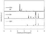
- the mass ratio of the aliphatic thiol ligand and the polar ligand coordinated on the surface of the semiconductor nanoparticles can be quantified using 1H-NMR.
- the obtained semiconductor nanoparticle composite is dispersed in a heavy solvent, electromagnetic waves are applied in a magnetic field to cause 1H nuclear magnetic resonance, and the free induction decay signal obtained at this time is Fourier analyzed to obtain a 1H-NMR spectrum. Since the 1H-NMR spectrum gives a characteristic signal at a position corresponding to the structure of the ligand type, the type of each ligand is identified from the position and the integrated intensity ratio of these signals, and the ratio is calculated.
- Examples of the deuterated solvent include CDCl 3 , acetone-d6, N-hexane-D14 and the like.
- the method of coordinating the ligand to the semiconductor nanoparticles is not limited, but a ligand exchange method utilizing the coordinating force of the ligand can be used.
- the semiconductor nanoparticles in which the organic compound used in the process of producing the semiconductor nanoparticles described above is coordinated with the surface of the semiconductor nanoparticles are brought into contact with the target ligand in a liquid phase.
- a semiconductor nanoparticle complex in which the target ligand is coordinated on the surface of the semiconductor nanoparticles can be obtained.
- a liquid phase reaction using a solvent as described later is usually carried out, but when the ligand to be used is a liquid under the reaction conditions, the ligand itself is used as a solvent and another solvent is not added. Is also possible.
- the desired ligand can be easily coordinated.
- a non-coordinating solvent is used in the synthesis of the semiconductor nanoparticles, the formation of defects on the surface of the semiconductor nanoparticles can be minimized when the desired ligand is coordinated, and the fluorescence quantum efficiency is lowered. Can be prevented.
- the semiconductor nanoparticle-containing dispersion after the semiconductor nanoparticles are produced is purified, redispersed, and then a solvent containing an aliphatic thiol ligand is added, and a solvent containing a polar ligand is further added to create a nitrogen atmosphere.
- the desired semiconductor nanoparticle composite can be obtained by stirring under 50 ° C. to 200 ° C. for 1 minute to 120 minutes.
- the aliphatic thiol ligand and the polar ligand may be added at the same time.
- the semiconductor nanoparticles and the semiconductor nanoparticle composite can be purified as follows.
- the semiconductor nanoparticle composite can be precipitated from the dispersion by adding a polarity conversion solvent such as acetone.
- the precipitated semiconductor nanoparticle composite can be recovered by filtration or centrifugation, while the supernatant containing unreacted starting material and other impurities can be discarded or reused.
- the precipitated semiconductor nanoparticle composite can then be washed with a further dispersion medium and dispersed again. This purification process can be repeated, for example, 2-4 times, or until the desired purity is reached.
- the method for purifying the semiconductor nanoparticle composite is not particularly limited, and in addition to the methods shown above, for example, aggregation, liquid-liquid extraction, distillation, electrodeposition, size exclusion chromatography and / or ultrafiltration and the like. Any method can be used alone or in combination.
- semiconductor nanoparticle composite dispersion As the semiconductor nanoparticle composite contained in the semiconductor nanoparticle composite dispersion liquid of the present invention, the above-mentioned configuration of the semiconductor nanoparticle composite of the present invention can be adopted.
- the state in which the semiconductor nanoparticle composite is dispersed in the dispersion medium means that the semiconductor nanoparticle composite does not precipitate when the semiconductor nanoparticle composite and the dispersion medium are mixed, or is visually recognizable. Indicates that the state does not remain as turbidity (cloudiness).
- a semiconductor nanoparticle composite dispersed in a dispersion medium is referred to as a semiconductor nanoparticle composite dispersion liquid.
- the semiconductor nanoparticle composite of the present invention can be dispersed in an organic dispersion medium to form a semiconductor nanoparticle composite dispersion liquid.
- the semiconductor nanoparticle composite of the present invention is dispersed in an organic dispersion medium having an SP value of 8.5 or more, an organic dispersion medium having an SP value of 9.0 or more, and an organic dispersion medium having an SP value of 10.0 or more.
- a semiconductor nanoparticle composite dispersion is formed.
- the SP value here is a Hildebrand solubility parameter, which is a value calculated from the Hansen solubility parameter.
- the Hansen solubility parameter is described in the handbook, eg, "Hansen Solubility Parameters: A User's Handbook", 2nd Edition, C.I. M. The values in Hanson (2007), Hanson and Abbot et al. It can be determined using the Practice (HSPiP) program (2nd edition) provided by.
- hexane, acetone, propylene glycol monomethyl ether acetate (PGMEA), propylene glycol monomethyl ether (PGME), isopropyl alcohol (IPA), and isopropyl alcohol (IPA) can be used as organic dispersion media. It is possible to disperse the semiconductor nanoparticles complex in any one or more organic dispersion media selected from the group consisting of isopropanol acrylate (IBOA), ethanol, and methanol.
- IBOA isopropanol acrylate
- ethanol ethanol
- methanol isopropyl alcohol
- organic dispersion medium polar organic dispersion media such as alcohols, ketones, esters, glycol ethers and glycol ether esters can be selected.
- polar organic dispersion media such as alcohols, ketones, esters, glycol ethers and glycol ether esters can be selected.
- the semiconductor nanoparticle composite can be used while maintaining the dispersibility when applied to dispersion in a cured film or resin described later.
- PGMEA and PGME are generally used as diluting solvents, and if the semiconductor nanoparticles composite can be dispersed in PGMEA and PGME, the semiconductor nanoparticles composite is widely applied to the photoresist field. can do.
- the semiconductor nanoparticle composite When the semiconductor nanoparticle composite has the above-mentioned structure, the semiconductor nanoparticle composite can be dispersed in an organic dispersion medium at a high mass fraction, and as a result, the semiconductor nanoparticles in the semiconductor nanoparticle composite dispersion liquid can be dispersed.
- the mass fraction of the above can be 20% by mass or more, further 25% by mass or more, and further 35% by mass or more.
- a monomer can be selected as a dispersion medium for the semiconductor nanoparticle composite dispersion liquid.
- the monomer is not particularly limited, but it is preferable that it is a (meth) acrylic monomer that can be widely selected for application of semiconductor nanoparticles.
- the (meth) acrylic monomer is methyl (meth) acrylate, ethyl (meth) acrylate, propyl (meth) acrylate, butyl (meth) acrylate, isobutyl (meth) acrylate, isoamyl, depending on the application of the semiconductor nanoparticle composite dispersion.
- the acrylic monomer may be one or a mixture of two or more selected from lauryl (meth) acrylate and 1,6-hexadioldi (meth) acrylate depending on the application of the semiconductor nanoparticle composite dispersion.
- a prepolymer can be selected as the dispersion medium of the semiconductor nanoparticle composite dispersion liquid.
- the prepolymer is not particularly limited, and examples thereof include an acrylic resin prepolymer, a silicone resin prepolymer, and an epoxy resin prepolymer.
- the semiconductor nanoparticle composite dispersion of the present invention preferably has a fluorescence quantum efficiency (QY) of 80% or more, more preferably 85% or more.
- QY fluorescence quantum efficiency
- the fluorescence quantum efficiency of the semiconductor nanoparticle composite dispersion can be measured using a quantum efficiency measurement system.
- a monomer or a prepolymer can be selected as the dispersion medium of the semiconductor nanoparticle composite dispersion liquid to form a semiconductor nanoparticle composite composition.
- the monomer or prepolymer is not particularly limited, and examples thereof include a radically polymerizable compound containing an ethylenically unsaturated bond, a siloxane compound, an epoxy compound, an isocyanate compound, and a phenol derivative. Further, a cross-linking agent may be added to the semiconductor nanoparticle composite composition.
- the cross-linking agent depends on the type of monomer in the semiconductor nanoparticle composite composition: polyfunctional (meth) acrylate, polyfunctional silane compound, polyfunctional amine, polyfunctional carboxylic acid, polyfunctional thiol, polyfunctional alcohol, and polyfunctional isocyanate. It is selected from.
- aliphatic hydrocarbons such as pentane, hexane, cyclohexane, isohexane, heptane, octane and petroleum ether, alcohols, ketones, esters, glycol ethers and glycol ether esters
- organic solvents that do not affect curing, such as aromatic hydrocarbons such as benzene, toluene, xylene and mineral spirits, and alkyl halides such as dichloromethane and chloroform.
- the above-mentioned organic solvent can be used not only for diluting the semiconductor nanoparticle composite composition but also as an organic dispersion medium. That is, it is also possible to disperse the semiconductor nanoparticle composite of the present invention in the above-mentioned organic solvent to obtain a semiconductor nanoparticle composite dispersion liquid.
- the semiconductor nanoparticle composite composition may be an appropriate initiator, scatterer, catalyst, binder, surfactant, adhesion accelerator, antioxidant, ultraviolet ray, depending on the type of monomer in the semiconductor nanoparticle composite composition. It may contain an absorbent, an anti-aggregation agent, a dispersant and the like. Further, in order to improve the optical properties of the semiconductor nanoparticle composite composition or the semiconductor nanoparticle composite cured film described later, the semiconductor nanoparticle composite composition may contain a scattering agent.
- the scattering agent is a metal oxide such as titanium oxide or zinc oxide, and the particle size of these is preferably 100 nm to 500 nm. From the viewpoint of the effect of scattering, the particle size of the scattering agent is more preferably 200 nm to 400 nm.
- the content of the scattering agent is preferably 2% by mass to 30% by mass with respect to the composition, and more preferably 5% by mass to 20% by mass from the viewpoint of maintaining the pattern property of the composition.
- the mass fraction of the semiconductor nanoparticles in the semiconductor nanoparticle composite composition can be 30% by mass or more.
- the semiconductor nanoparticles composite and the semiconductor nanoparticles also have a high mass fraction in the cured film described later. Can be dispersed.
- the absorbance of the film with respect to light having a wavelength of 450 nm from the normal direction is preferably 1.0 or more, preferably 1.3 or more. More preferably, it is more preferably 1.5 or more. As a result, the light from the backlight can be efficiently absorbed, so that the thickness of the cured film described later can be reduced, and the device to be applied can be miniaturized.
- the diluted composition is obtained by diluting the above-mentioned semiconductor nanoparticle composite composition of the present invention with an organic solvent.
- the organic solvent for diluting the semiconductor nanoparticle composite composition is not particularly limited, and for example, aliphatic hydrocarbons such as pentane, hexane, cyclohexane, isohexane, heptane, octane and petroleum ether, alcohols and ketones. Classes, esters, glycol ethers, glycol ether esters, aromatic hydrocarbons such as benzene, toluene, xylene and mineral spirit, and alkyl halides such as dichloromethane and chloroform. Among these, glycol ethers and glycol ether esters are preferable from the viewpoint of solubility in a wide range of resins and film uniformity at the time of coating film.
- the semiconductor nanoparticle composite cured film is a film containing a semiconductor nanoparticle composite and represents a cured film.
- the semiconductor nanoparticle composite cured film can be obtained by curing the above-mentioned semiconductor nanoparticle composite composition or diluted composition into a film.
- the semiconductor nanoparticle composite cured film contains a semiconductor nanoparticle, a ligand coordinated on the surface of the semiconductor nanoparticle, and a polymer matrix.
- the polymer matrix is not particularly limited, and examples thereof include (meth) acrylic resin, silicone resin, epoxy resin, silicone resin, maleic acid resin, butyral resin, polyester resin, melamine resin, phenol resin, and polyurethane resin.
- a semiconductor nanoparticle composite cured film may be obtained by curing the semiconductor nanoparticle composite composition described above.
- the semiconductor nanoparticle composite cured film may further contain a cross-linking agent.
- the method for curing the film is not particularly limited, but the film can be cured by a curing method suitable for the composition constituting the film, such as heat treatment and ultraviolet treatment.
- Semiconductor nanoparticle composite The ligand contained in the cured film and coordinated to the surface of the semiconductor nanoparticles and the semiconductor nanoparticles preferably constitutes the semiconductor nanoparticle composite described above.
- the semiconductor nanoparticle composite can be dispersed in the cured film at a higher mass fraction. It is possible.
- the mass fraction of the semiconductor nanoparticles in the cured film of the semiconductor nanoparticle composite is preferably 30% by mass or more, and more preferably 40% by mass or more. However, when it is 70% by mass or more, the amount of the composition constituting the film is reduced, and it becomes difficult to cure and form the film.
- the absorbance of the semiconductor nanoparticle composite cured film can be increased.
- the absorbance is preferably 1.0 or more, preferably 1.3 or more, with respect to light having a wavelength of 450 nm from the normal direction of the semiconductor nanoparticle composite cured film. More preferably, it is more preferably 1.5 or more.
- the semiconductor nanoparticle composite cured film of the present invention contains a semiconductor nanoparticle composite having high light emitting characteristics, it is possible to provide a semiconductor nanoparticle composite cured film having high light emitting characteristics.
- the fluorescence quantum efficiency of the cured film of the semiconductor nanoparticle composite is preferably 70% or more, and more preferably 80% or more.
- the thickness of the semiconductor nanoparticle composite cured film is preferably 50 ⁇ m or less, more preferably 20 ⁇ m or less, and more preferably 10 ⁇ m or less in order to miniaturize the device to which the semiconductor nanoparticle composite cured film is applied. Is even more preferable.
- the semiconductor nanoparticle composite patterning film can be obtained by forming a film-like pattern of the above-mentioned semiconductor nanoparticle composite composition or dilution composition.
- the method for patterning the semiconductor nanoparticle composite composition and the diluted composition is not particularly limited, and examples thereof include spin coating, bar coating, inkjet, screen printing, and photolithography.
- the display element uses the above-mentioned semiconductor nanoparticle composite patterning film. For example, by using a semiconductor nanoparticle composite patterning film as a wavelength conversion layer, it is possible to provide a display element having excellent fluorescence quantum efficiency.
- the semiconductor nanoparticle composite dispersion liquid of the present invention adopts the following constitution.
- the semiconductor nanoparticle complex comprises two or more ligands including an aliphatic thiol ligand and a polar ligand, and semiconductor nanoparticles in which the ligand is coordinated on the surface.
- the ligand consists of an organic group and a coordinating group.
- the polar ligand contains a hydrophilic functional group in the organic group.
- the SP value of the organic dispersion medium is 8.5 or more.
- (2) The SP value of the organic dispersion medium is 9.0 or more.
- the organic dispersion medium is one or more mixed dispersion media selected from the group consisting of alcohols, ketones, esters, glycol ethers, and glycol ether esters.
- the organic dispersion medium is one or more mixed dispersion media selected from acetone, PGMEA, PGME, IPA, ethanol, and methanol.
- the organic dispersion medium is one or more mixed dispersion media selected from the group consisting of glycol ethers and glycol ether esters.
- the organic dispersion medium is one or more mixed dispersion media selected from the group consisting of PGMEA and PGME.
- the fluorescence quantum efficiency of the semiconductor nanoparticle composite dispersion is 80% or more.
- the mass ratio of the aliphatic thiol ligand to the polar ligand (aliphatic thiol ligand / polar ligand) is 0.05 to 1.00.
- the aliphatic thiol ligand has 6 to 14 carbon atoms.
- the aliphatic thiol ligand is one or more of hexanethiol, octanethiol, and dodecanethiol.
- the molecular weight of the polar ligand is 600 or less.
- (12) The molecular weight of the polar ligand is 450 or less.
- the organic group of the polar ligand has at least one of a hydroxyl group, a carboxyl group, a carbonyl group, an amino group, an ether bond, an ester bond and a siloxane bond.
- the organic group of the polar ligand has an ether bond.
- the coordinating group of the polar ligand is a mercapto group or a carboxyl group.
- the coordinating group of the polar ligand is a mercapto group.
- the total mass fraction of the aliphatic thiol ligand and the polar ligand in the entire surface ligand is 0.7 or more.
- the total mass fraction of the aliphatic thiol ligand and the polar ligand in the entire surface ligand is 0.8 or more.
- (19) Zn is contained in the surface composition of the semiconductor nanoparticles.
- the fluorescence quantum efficiency of the semiconductor nanoparticle composite is 80% or more.
- the fluorescence quantum efficiency of the semiconductor nanoparticle composite is 85% or more.
- the half width of the emission spectrum of the semiconductor nanoparticle composite is 40 nm or less.
- the half width of the emission spectrum of the semiconductor nanoparticle composite is 35 nm or less.
- the semiconductor nanoparticles contain In and P.
- the mass fraction of the semiconductor nanoparticles with respect to the semiconductor nanoparticle composite dispersion is 20% by mass or more.
- the mass fraction of the semiconductor nanoparticles with respect to the semiconductor nanoparticle composite dispersion is 25% by mass or more.
- the organic dispersion medium is a monomer or a prepolymer.
- the semiconductor nanoparticle composite composition and the semiconductor nanoparticle composite cured film of the present invention can be produced by the following production methods.
- (28) A method for producing a semiconductor nanoparticle composite composition. Add either or both of the cross-linking agent and the dispersion medium to the semiconductor nanoparticle composite dispersion liquid according to any one of (1) to (27) above.
- a method for producing a semiconductor nanoparticle composite composition A method for producing a semiconductor nanoparticle composite composition.
- the semiconductor nanoparticle composite composition obtained by the method for producing a semiconductor nanoparticle composite composition according to (28) above is cured.
- the semiconductor nanoparticle composite of the present invention adopts the following constitution.
- ⁇ 1> A semiconductor nanoparticle complex in which two or more ligands including an aliphatic thiol ligand and a polar ligand are coordinated on the surface of semiconductor nanoparticles.
- the ligand consists of an organic group and a coordinating group.
- the organic group is an aliphatic hydrocarbon group and the coordinating group is a mercapto group.
- the polar ligand contains a hydrophilic functional group in the organic group.
- the mass ratio of the aliphatic thiol ligand to the polar ligand is 0.05 to 1.00.
- the organic dispersion medium is one or more mixed dispersion media selected from the group consisting of alcohols, glycol ethers, and glycol ether esters.
- the organic dispersion medium is one or more mixed dispersion media selected from the group consisting of acetone, PGMEA, PGME, IPA, ethanol, and methanol.
- ⁇ 6> The aliphatic thiol ligand has 6 to 14 carbon atoms.
- the aliphatic thiol ligand is one or more of hexanethiol, octanethiol, decanethiol and dodecanethiol.
- the molecular weight of the polar ligand is 600 or less.
- ⁇ 9> The molecular weight of the polar ligand is 450 or less.
- the total mass fraction of the aliphatic thiol ligand and the polar ligand in the entire ligand is 0.7 or more.
- ⁇ 11> The total mass fraction of the aliphatic thiol ligand and the polar ligand in the entire ligand is 0.8 or more.
- the organic group of the polar ligand has at least one of a hydroxyl group, a carboxyl group, a carbonyl group, an amino group, an ether bond, an ester bond and a siloxane bond.
- the organic group of the polar ligand contains an ether bond.
- the coordinating group of the polar ligand is a mercapto group or a carboxyl group.
- the coordinating group of the polar ligand is a mercapto group.
- the semiconductor nanoparticle composite can be dispersed in the organic dispersion medium, and can be dispersed so that the mass fraction of the semiconductor nanoparticles is 20% by mass or more.
- the semiconductor nanoparticle composite can be dispersed in the organic dispersion medium, and can be dispersed so that the mass fraction of the semiconductor nanoparticles is 25% by mass or more.
- ⁇ 18> The fluorescence quantum efficiency of the semiconductor nanoparticle composite is 80% or more.
- the fluorescence quantum efficiency of the semiconductor nanoparticle composite is 85% or more.
- the semiconductor nanoparticle composite according to any one of ⁇ 1> to ⁇ 18> above. ⁇ 20> The half width of the emission spectrum of the semiconductor nanoparticle composite is 40 nm or less.
- the semiconductor nanoparticle composite according to any one of ⁇ 1> to ⁇ 19> above. ⁇ 21> The half width of the emission spectrum of the semiconductor nanoparticle composite is 35 nm or less.
- the semiconductor nanoparticles contain In and P.
- ⁇ 23> The semiconductor nanoparticles contain Zn on the surface of the semiconductor nanoparticles.
- the semiconductor nanoparticle composite dispersion liquid of the present invention adopts the following constitution.
- ⁇ 24> A semiconductor nanoparticle composite dispersion liquid in which the semiconductor nanoparticle composite according to any one of ⁇ 1> to ⁇ 23> above is dispersed in an organic dispersion medium.
- the semiconductor nanoparticle composite composition of the present invention adopts the following constitution. ⁇ 25> A semiconductor nanoparticle composite composition in which the semiconductor nanoparticle composite according to any one of ⁇ 1> to ⁇ 23> above is dispersed in a dispersion medium.
- the dispersion medium is a monomer or prepolymer, Semiconductor nanoparticle composite composition.
- the semiconductor nanoparticle composite cured film of the present invention adopts the following constitution. ⁇ 26>
- the semiconductor nanoparticle composite according to any one of ⁇ 1> to ⁇ 23> above is dispersed in the polymer matrix.
- Example 1 An InP-based semiconductor nanoparticle composite was produced according to the following method.
- core Indium acetate (0.3 mmol) and zinc oleate (0.6 mmol) are added to a mixture of oleic acid (0.9 mmol), 1-dodecanethiol (0.1 mmol) and octadecene (10 mL) under vacuum ( ⁇ 20 Pa).
- oleic acid 0.9 mmol
- 1-dodecanethiol 0.1 mmol
- octadecene 10 mL
- the mixture reacted under vacuum was placed in a nitrogen atmosphere at 25 ° C., tris (trimethylsilyl) phosphine (0.2 mmol) was added, and then the mixture was heated to about 300 ° C. and reacted for 10 minutes.
- the reaction solution was cooled to 25 ° C., octanoic acid chloride (0.45 mmol) was injected, and the mixture was heated at about 250 ° C. for 30 minutes and then cooled to 25 ° C. to obtain a dispersion of InP-based semiconductor nanoparticles.
- octanoic acid chloride (0.45 mmol) was injected, and the mixture was heated at about 250 ° C. for 30 minutes and then cooled to 25 ° C. to obtain a dispersion of InP-based semiconductor nanoparticles.
- a shell was formed on the surface of the core as shown below to produce core-shell type semiconductor nanoparticles, and the optical characteristics were measured.
- the reaction solution was filtered and the filtrate was diluted with chloroform.
- the solution was extracted in the order of 10% HCl aqueous solution, 10% Na 2 CO 3 aqueous solution, and saturated NaCl aqueous solution, and the organic phase was recovered.
- the organic phase was concentrated by evaporation and then purified by column chromatography using a hexane-ethyl acetate mixed solvent as a developing solvent to obtain the desired product.
- the precipitate was dissolved in 1M NaOH solution (40 mL), NaCl (10 g) was added, and the mixture was stirred at room temperature for 1 hour to remove the ethyl group at the end of PEG. This solution was adjusted to pH 3.0 by adding 6M HCl. The obtained solution was extracted with a chloroform-aqueous system to obtain PEG-COOH having a molecular weight of 400.
- a semiconductor nanoparticle 1-octadecene dispersion was prepared by dispersing the purified semiconductor nanoparticles in 1-octadecene so as to have a mass ratio of 10% by mass in a flask. 10.0 g of the prepared semiconductor nanoparticles 1-octadecene dispersion was placed in a flask, 0.2 g of dodecanethiol (DDT) was added as an aliphatic thiol ligand, and 4 g of PEG-SH was added as a polar ligand, and the atmosphere was nitrogen. The mixture was stirred at 110 ° C. for 60 minutes and cooled to 25 ° C.
- DDT dodecanethiol
- the reaction solution containing the semiconductor nanoparticle composite was transferred to a centrifuge tube and centrifuged at 4000 G for 20 minutes to separate into a transparent 1-octadecene phase and a semiconductor nanoparticle composite phase.
- the 1-octadecene phase was removed and the remaining semiconductor nanoparticle composite phase was recovered.
- 5.0 mL of acetone was added to the obtained semiconductor nanoparticle composite phase to prepare a dispersion.
- 50 mL of normal hexane was added to the obtained dispersion, and the mixture was centrifuged at 4000 G for 20 minutes. After centrifugation, the clear supernatant was removed and the precipitate was collected. This operation was repeated several times to obtain a purified semiconductor nanoparticle composite.
- the optical properties of the semiconductor nanoparticle composite were measured using a fluorescence quantum efficiency measurement system (QE-2100, manufactured by Otsuka Electronics Co., Ltd.).
- the obtained semiconductor nanoparticle composite was dispersed in a dispersion medium, and a single light of 450 nm was applied to obtain an emission spectrum.
- the reexcited fluorescence emission spectrum obtained by reexcitation and fluorescence emission from the obtained emission spectrum was obtained.
- the fluorescence quantum efficiency (QY) and half-value width (FWHM) were calculated from the removed emission spectrum after re-excitation correction.
- PGMEA was used as the dispersion medium.
- PGMEA was used as the organic dispersion medium, and the dispersion state when the mass fraction of the semiconductor nanoparticles was set to 20% by mass to 35% by mass was observed, ⁇ was observed for the dispersed one, and precipitation and turbidity were observed. The ones marked with x are marked.
- a mixed dispersion medium mixed at a volume ratio of 1: 1 was used.
- FIG. 1 is a result of measuring the semiconductor nanoparticle composite produced in Example 1 by 1H-NMR. Signals were observed around 0.8 ppm to 2.5 ppm, 3.5 ppm to 4.0 ppm, and 5.4 ppm. Note that FIG. 2 shows 1H-NMR spectra of dodecanethiol, oleic acid and PEG-SH. From FIGS.
- the signal of about 0.8 ppm to 2.5 ppm is for dodecanethiol and oleic acid
- the signal of 3.5 ppm to 4.0 ppm is for PEG-SH
- the signal is about 5.4 ppm.
- the type and abundance ratio of the ligand can be determined from the position and peak area of each signal from the 1H-NMR spectrum.
- Example 2 In the step of producing the semiconductor nanoparticle composite, the semiconductor nanoparticle composite was prepared in the same manner as in Example 1 except that 0.5 g of dodecanethiol was used as the aliphatic thiol ligand and 4.0 g of PEG-SH was used as the polar ligand.
- Example 3 Example 1 except that 1.0 g of dodecanethiol was used as an aliphatic thiol ligand, 1.5 g of PEG-SH was used as a polar ligand, and 0.5 g of oleic acid was further added in the step of preparing the semiconductor nanoparticle composite.
- a semiconductor nanoparticle composite was obtained in the same manner as in.
- Example 4 In the process of preparing the semiconductor nanoparticle complex, 1.0 g of dodecanethiol as an aliphatic thiol ligand and 1.5 g of N-acetyl-N- (2-mercaptoethyl) propanamide as a polar ligand were used, and oleic acid was further added. A semiconductor nanoparticle composite was obtained in the same manner as in Example 1 except that 0.5 g was added.
- Example 5 In the step of preparing the semiconductor nanoparticle complex, 0.3 g of dodecanethiol and 0.2 g of hexanethiol were used as aliphatic thiol ligands, and 4.0 g of PEG-SH was used as a polar ligand. A semiconductor nanoparticle composite was obtained in the same manner as in Example 1.
- Example 6 In the process of preparing the semiconductor nanoparticle complex, 0.2 g of dodecanethiol as an aliphatic thiol ligand, 1.5 g of triethylene glycol monomethylthiol (TEG-SH) as a polar ligand, and 0.5 g of oleic acid were used. A semiconductor nanoparticle composite was obtained in the same manner as in Example 1 except that it was added.
- TAG-SH triethylene glycol monomethylthiol
- Example 7 Examples except that 0.5 g of octanethiol was used as the aliphatic thiol ligand and 4.0 g of N-acetyl-N- (2-mercaptoethyl) propanamide was used as the polar ligand in the step of preparing the semiconductor nanoparticle composite.
- a semiconductor nanoparticle composite was obtained in the same manner as in 1.
- Example 8 Examples except that 0.5 g of hexanethiol was used as the aliphatic thiol ligand and 4.0 g of N-acetyl-N- (2-mercaptoethyl) propanamide was used as the polar ligand in the step of preparing the semiconductor nanoparticle composite.
- a semiconductor nanoparticle composite was obtained in the same manner as in 1.
- Example 9 In the step of producing the semiconductor nanoparticle composite, the semiconductor nanoparticle composite was prepared in the same manner as in Example 1 except that 0.5 g of hexanethiol was used as the aliphatic thiol ligand and 4.0 g of PEG-SH was used as the polar ligand.
- Example 10 Examples except that 1.0 g of decanethiol was used as the aliphatic thiol ligand and 4.0 g of N-acetyl-N- (2-mercaptoethyl) propanamide was used as the polar ligand in the step of preparing the semiconductor nanoparticle composite.
- a semiconductor nanoparticle composite was obtained in the same manner as in 1.
- Example 11 In the step of producing the semiconductor nanoparticle composite, a semiconductor was used in the same manner as in Example 1 except that 0.2 g of dodecanethiol was used as the aliphatic thiol ligand and 6.0 g of PEG-COOH (molecular weight 400) was used as the polar ligand. A nanoparticle composite was obtained.
- Example 12 In the process of preparing the semiconductor nanoparticle complex, except that 0.5 g of dodecanethiol was used as an aliphatic thiol ligand, 2.0 g of methyl 3-mercaptopropionate was used as a polar ligand, and 0.5 g of oleic acid was further added.
- a semiconductor nanoparticle composite was obtained in the same manner as in Example 1.
- Example 13 In the step of producing the semiconductor nanoparticle composite, a semiconductor was used in the same manner as in Example 1 except that 0.5 g of dodecanethiol was used as the aliphatic thiol ligand and 6.0 g of PEG-COOH (molecular weight 600) was used as the polar ligand. A nanoparticle composite was obtained.
- Example 14 In the step of producing the semiconductor nanoparticle composite, a semiconductor was used in the same manner as in Example 1 except that 0.5 g of dodecanethiol was used as the aliphatic thiol ligand and 7.5 g of PEG-COOH (molecular weight 750) was used as the polar ligand. A nanoparticle composite was obtained.
- Example 15 In the step of producing the semiconductor nanoparticle composite, a semiconductor was used in the same manner as in Example 1 except that 0.5 g of dodecanethiol was used as the aliphatic thiol ligand and 10.0 g of PEG-COOH (molecular weight 1000) was used as the polar ligand. A nanoparticle composite was obtained.
- Example 16 Example 1 except that 0.5 g of dodecanethiol was used as an aliphatic thiol ligand, 4.0 g of PEG-SH was used as a polar ligand, and 1.5 g of oleic acid was further added in the step of preparing the semiconductor nanoparticle composite. A semiconductor nanoparticle composite was obtained in the same manner as in.
- Example 1 Example 1 except that 4.0 g of PEG-SH was used as a polar ligand and 4.0 g of tributylphosphine (TBP) was further added in the step of preparing the semiconductor nanoparticle composite without adding an aliphatic thiol ligand.
- TBP tributylphosphine
- Example 3 The flask contained 1.0 g of the semiconductor nanoparticle composite purified in the same manner as in Example 1, 10 mL of isopropanol, and 4.0 g of PEG-SH. The solution was stirred at 80 ° C. for 180 minutes under a nitrogen atmosphere and cooled to 25 ° C. 50 mL of normal hexane was added to the reaction solution, and the mixture was centrifuged at 4000 G for 20 minutes. After centrifugation, the clear supernatant was removed and the precipitate was collected. 5.0 mL of acetone was added to the precipitate to prepare a dispersion.
- the emission characteristics of the obtained semiconductor nanoparticle composite, the ligand mass ratio, and the dispersion state in the dispersion medium are shown in Tables 1-1 to 1-7.
Landscapes
- Chemical & Material Sciences (AREA)
- Organic Chemistry (AREA)
- Engineering & Computer Science (AREA)
- Materials Engineering (AREA)
- Inorganic Chemistry (AREA)
- Life Sciences & Earth Sciences (AREA)
- Wood Science & Technology (AREA)
- Chemical Kinetics & Catalysis (AREA)
- Nanotechnology (AREA)
- Health & Medical Sciences (AREA)
- Polymers & Plastics (AREA)
- Medicinal Chemistry (AREA)
- Physics & Mathematics (AREA)
- Microelectronics & Electronic Packaging (AREA)
- Condensed Matter Physics & Semiconductors (AREA)
- Power Engineering (AREA)
- Crystallography & Structural Chemistry (AREA)
- Manufacturing & Machinery (AREA)
- General Physics & Mathematics (AREA)
- General Chemical & Material Sciences (AREA)
- Optics & Photonics (AREA)
- Ceramic Engineering (AREA)
- Composite Materials (AREA)
- Biophysics (AREA)
- Computer Hardware Design (AREA)
- Luminescent Compositions (AREA)
- Led Device Packages (AREA)
Abstract
L'invention concerne un liquide de dispersion de complexe de nanoparticules semi-conductrices dans lequel des nanoparticules semi-conductrices sont dispersées dans un milieu de dispersion polaire à une fraction massique élevée, et dans laquelle un rendement quantique de fluorescence élevée (QY) est maintenu. Selon un mode de réalisation, un liquide de dispersion de complexe de nanoparticules semi-conductrices comprend un complexe de nanoparticules semi-conductrices dispersées dans un milieu de dispersion organique, la nanoparticule semi-conductrice étant constituée de deux ligands ou plus dont un ligand thiol aliphatique et un ligand polaire, et une nanoparticule semi-conductrice avec lesdits ligands coordonnés sur sa surface ; les ligands sont composés d'un groupe organique et d'un groupe de coordination ; le groupe organique du ligand polaire comprend un groupe fonctionnel hydrophile ; et la valeur de paramètre de solubilité du milieu de dispersion organique est de 8,5 ou plus.
Priority Applications (4)
| Application Number | Priority Date | Filing Date | Title |
|---|---|---|---|
| JP2021521903A JPWO2020241872A1 (fr) | 2019-05-31 | 2020-05-29 | |
| CN202080040145.8A CN113906116A (zh) | 2019-05-31 | 2020-05-29 | 半导体纳米粒子复合体分散液、半导体纳米粒子复合体、半导体纳米粒子复合体组合物和半导体纳米粒子复合体固化膜 |
| KR1020217039052A KR20220015399A (ko) | 2019-05-31 | 2020-05-29 | 반도체 나노입자 복합체 분산액, 반도체 나노입자 복합체, 반도체 나노입자 복합체 조성물 및 반도체 나노입자 복합체 경화막 |
| US17/595,923 US20220315834A1 (en) | 2019-05-31 | 2020-05-29 | Semiconductor nanoparticle complex dispersion liquid, semiconductor nanoparticle complex, semiconductor nanoparticle complex composition and semiconductor nanoparticle complex cured membrane |
Applications Claiming Priority (4)
| Application Number | Priority Date | Filing Date | Title |
|---|---|---|---|
| JP2019-103239 | 2019-05-31 | ||
| JP2019103239 | 2019-05-31 | ||
| JP2019-103240 | 2019-05-31 | ||
| JP2019103240 | 2019-05-31 |
Publications (1)
| Publication Number | Publication Date |
|---|---|
| WO2020241872A1 true WO2020241872A1 (fr) | 2020-12-03 |
Family
ID=73551919
Family Applications (1)
| Application Number | Title | Priority Date | Filing Date |
|---|---|---|---|
| PCT/JP2020/021464 WO2020241872A1 (fr) | 2019-05-31 | 2020-05-29 | Liquide de dispersion de complexe de nanoparticules semi-conductrices, complexe de nanoparticules semi-conductrices, composition de complexe de nanoparticules semi-conductrices et membrane durcie de complexe de nanoparticules semi-conductrices |
Country Status (6)
| Country | Link |
|---|---|
| US (1) | US20220315834A1 (fr) |
| JP (1) | JPWO2020241872A1 (fr) |
| KR (1) | KR20220015399A (fr) |
| CN (1) | CN113906116A (fr) |
| TW (1) | TW202112651A (fr) |
| WO (1) | WO2020241872A1 (fr) |
Citations (5)
| Publication number | Priority date | Publication date | Assignee | Title |
|---|---|---|---|---|
| WO2017038487A1 (fr) * | 2015-08-31 | 2017-03-09 | 富士フイルム株式会社 | Nanoparticules semi-conductrices, liquide de dispersion, film et procédé de production de nanoparticules semi-conductrices |
| WO2018226654A1 (fr) * | 2017-06-05 | 2018-12-13 | Austin Smith | Stabilisation d'acide de concentrés et prémélanges de résine à points quantiques |
| WO2018224459A1 (fr) * | 2017-06-08 | 2018-12-13 | Merck Patent Gmbh | Composition comprenant des nanoparticules semi-conductrices électroluminescentes ayant des ligands de surface fonctionnels thiol |
| WO2018226925A1 (fr) * | 2017-06-07 | 2018-12-13 | Nanosys, Inc. | Ligands hydrophiles thiolés améliorant la fiabilité des points quantiques dans des films de résine |
| WO2019008374A1 (fr) * | 2017-07-05 | 2019-01-10 | Nanoco Technologies Ltd | Architectures de points quantiques pour applications de filtre coloré |
Family Cites Families (1)
| Publication number | Priority date | Publication date | Assignee | Title |
|---|---|---|---|---|
| JP5881045B2 (ja) | 2011-10-11 | 2016-03-09 | 国立研究開発法人産業技術総合研究所 | 量子ドット含有チタン化合物及びその製造方法、並びに該量子ドット含有チタン化合物を用いた光電変換素子 |
-
2020
- 2020-05-29 CN CN202080040145.8A patent/CN113906116A/zh active Pending
- 2020-05-29 TW TW109118000A patent/TW202112651A/zh unknown
- 2020-05-29 KR KR1020217039052A patent/KR20220015399A/ko unknown
- 2020-05-29 JP JP2021521903A patent/JPWO2020241872A1/ja active Pending
- 2020-05-29 WO PCT/JP2020/021464 patent/WO2020241872A1/fr active Application Filing
- 2020-05-29 US US17/595,923 patent/US20220315834A1/en active Pending
Patent Citations (5)
| Publication number | Priority date | Publication date | Assignee | Title |
|---|---|---|---|---|
| WO2017038487A1 (fr) * | 2015-08-31 | 2017-03-09 | 富士フイルム株式会社 | Nanoparticules semi-conductrices, liquide de dispersion, film et procédé de production de nanoparticules semi-conductrices |
| WO2018226654A1 (fr) * | 2017-06-05 | 2018-12-13 | Austin Smith | Stabilisation d'acide de concentrés et prémélanges de résine à points quantiques |
| WO2018226925A1 (fr) * | 2017-06-07 | 2018-12-13 | Nanosys, Inc. | Ligands hydrophiles thiolés améliorant la fiabilité des points quantiques dans des films de résine |
| WO2018224459A1 (fr) * | 2017-06-08 | 2018-12-13 | Merck Patent Gmbh | Composition comprenant des nanoparticules semi-conductrices électroluminescentes ayant des ligands de surface fonctionnels thiol |
| WO2019008374A1 (fr) * | 2017-07-05 | 2019-01-10 | Nanoco Technologies Ltd | Architectures de points quantiques pour applications de filtre coloré |
Also Published As
| Publication number | Publication date |
|---|---|
| CN113906116A (zh) | 2022-01-07 |
| KR20220015399A (ko) | 2022-02-08 |
| JPWO2020241872A1 (fr) | 2020-12-03 |
| TW202112651A (zh) | 2021-04-01 |
| US20220315834A1 (en) | 2022-10-06 |
Similar Documents
| Publication | Publication Date | Title |
|---|---|---|
| JP7354659B2 (ja) | 半導体ナノ粒子複合体、半導体ナノ粒子複合体分散液、半導体ナノ粒子複合体組成物および半導体ナノ粒子複合体硬化膜 | |
| WO2020241874A1 (fr) | Composition de complexe de nanoparticules semi-conductrices, composition de dilution, membrane durcie de complexe de nanoparticules semi-conductrices, membrane de formation de motifs de complexe de nanoparticules semi-conductrices, élément d'affichage, et liquide de dispersion de complexe de nanoparticules semi-conductrices | |
| WO2020241872A1 (fr) | Liquide de dispersion de complexe de nanoparticules semi-conductrices, complexe de nanoparticules semi-conductrices, composition de complexe de nanoparticules semi-conductrices et membrane durcie de complexe de nanoparticules semi-conductrices | |
| JP7468525B2 (ja) | 半導体ナノ粒子複合体、半導体ナノ粒子複合体分散液、半導体ナノ粒子複合体組成物および半導体ナノ粒子複合体硬化膜 | |
| US20220259492A1 (en) | Semiconductor nanoparticle complex, semiconductor nanoparticle complex dispersion liquid, semiconductor nanoparticle complex composition, and semiconductor nanoparticle complex cured film | |
| JP7476893B2 (ja) | 半導体ナノ粒子複合体、半導体ナノ粒子複合体分散液、半導体ナノ粒子複合体組成物、半導体ナノ粒子複合体硬化膜および半導体ナノ粒子複合体の精製方法 | |
| WO2020241873A1 (fr) | Complexe de nanoparticules semi-conductrices, composition de complexe de nanoparticules semi-conductrices, membrane durcie de complexe de nanoparticules semi-conductrices, liquide de dispersion de complexe de nanoparticules semi-conductrices, procédé de fabrication d'une composition de complexe de nanoparticules semi-conductrices et procédé de fabrication d'une membrane durcie de complexe de nanoparticules semi-conductrices | |
| WO2020241875A1 (fr) | Matériau composite de nanoparticules semi-conductrices | |
| TWI833967B (zh) | 半導體奈米粒子複合體、半導體奈米粒子複合體分散液、半導體奈米粒子複合體組成物及半導體奈米粒子複合體硬化膜 | |
| TWI839526B (zh) | 半導體奈米粒子複合體組成物、稀釋組成物、半導體奈米粒子複合體硬化膜、半導體奈米粒子複合體圖案化膜及顯示元件 | |
| TW202411401A (zh) | 半導體奈米粒子複合體、半導體奈米粒子複合體分散液、半導體奈米粒子複合體組成物及半導體奈米粒子複合體硬化膜 | |
| JP2024072840A (ja) | 半導体ナノ粒子複合体、半導体ナノ粒子複合体分散液、半導体ナノ粒子複合体組成物、半導体ナノ粒子複合体硬化膜および半導体ナノ粒子複合体の精製方法 | |
| JP6973469B2 (ja) | 半導体ナノ粒子集合体、半導体ナノ粒子集合体分散液、半導体ナノ粒子集合体組成物及び半導体ナノ粒子集合体硬化膜 | |
| JP2024054513A (ja) | 量子ドット含有組成物とその製造方法 | |
| JP2021123724A (ja) | 量子ドット、これを含む量子ドット分散体、硬化性組成物、硬化膜、及び画像表示装置 |
Legal Events
| Date | Code | Title | Description |
|---|---|---|---|
| 121 | Ep: the epo has been informed by wipo that ep was designated in this application |
Ref document number: 20815421 Country of ref document: EP Kind code of ref document: A1 |
|
| ENP | Entry into the national phase |
Ref document number: 2021521903 Country of ref document: JP Kind code of ref document: A |
|
| NENP | Non-entry into the national phase |
Ref country code: DE |
|
| 122 | Ep: pct application non-entry in european phase |
Ref document number: 20815421 Country of ref document: EP Kind code of ref document: A1 |