WO2020235083A1 - 光検査回路および光検査方法 - Google Patents
光検査回路および光検査方法 Download PDFInfo
- Publication number
- WO2020235083A1 WO2020235083A1 PCT/JP2019/020473 JP2019020473W WO2020235083A1 WO 2020235083 A1 WO2020235083 A1 WO 2020235083A1 JP 2019020473 W JP2019020473 W JP 2019020473W WO 2020235083 A1 WO2020235083 A1 WO 2020235083A1
- Authority
- WO
- WIPO (PCT)
- Prior art keywords
- optical
- light
- optical waveguide
- photodiode
- modulator
- Prior art date
- Legal status (The legal status is an assumption and is not a legal conclusion. Google has not performed a legal analysis and makes no representation as to the accuracy of the status listed.)
- Ceased
Links
Images



Classifications
-
- G—PHYSICS
- G02—OPTICS
- G02F—OPTICAL DEVICES OR ARRANGEMENTS FOR THE CONTROL OF LIGHT BY MODIFICATION OF THE OPTICAL PROPERTIES OF THE MEDIA OF THE ELEMENTS INVOLVED THEREIN; NON-LINEAR OPTICS; FREQUENCY-CHANGING OF LIGHT; OPTICAL LOGIC ELEMENTS; OPTICAL ANALOGUE/DIGITAL CONVERTERS
- G02F1/00—Devices or arrangements for the control of the intensity, colour, phase, polarisation or direction of light arriving from an independent light source, e.g. switching, gating or modulating; Non-linear optics
- G02F1/01—Devices or arrangements for the control of the intensity, colour, phase, polarisation or direction of light arriving from an independent light source, e.g. switching, gating or modulating; Non-linear optics for the control of the intensity, phase, polarisation or colour
- G02F1/015—Devices or arrangements for the control of the intensity, colour, phase, polarisation or direction of light arriving from an independent light source, e.g. switching, gating or modulating; Non-linear optics for the control of the intensity, phase, polarisation or colour based on semiconductor elements having potential barriers, e.g. having a PN or PIN junction
- G02F1/025—Devices or arrangements for the control of the intensity, colour, phase, polarisation or direction of light arriving from an independent light source, e.g. switching, gating or modulating; Non-linear optics for the control of the intensity, phase, polarisation or colour based on semiconductor elements having potential barriers, e.g. having a PN or PIN junction in an optical waveguide structure
-
- G—PHYSICS
- G01—MEASURING; TESTING
- G01M—TESTING STATIC OR DYNAMIC BALANCE OF MACHINES OR STRUCTURES; TESTING OF STRUCTURES OR APPARATUS, NOT OTHERWISE PROVIDED FOR
- G01M11/00—Testing of optical apparatus; Testing structures by optical methods not otherwise provided for
-
- G—PHYSICS
- G01—MEASURING; TESTING
- G01M—TESTING STATIC OR DYNAMIC BALANCE OF MACHINES OR STRUCTURES; TESTING OF STRUCTURES OR APPARATUS, NOT OTHERWISE PROVIDED FOR
- G01M11/00—Testing of optical apparatus; Testing structures by optical methods not otherwise provided for
- G01M11/30—Testing of optical devices, constituted by fibre optics or optical waveguides
- G01M11/33—Testing of optical devices, constituted by fibre optics or optical waveguides with a light emitter being disposed at one fibre or waveguide end-face, and a light receiver at the other end-face
- G01M11/333—Testing of optical devices, constituted by fibre optics or optical waveguides with a light emitter being disposed at one fibre or waveguide end-face, and a light receiver at the other end-face using modulated input signals
Definitions
- the present invention relates to an optical inspection circuit and an optical inspection method for inspecting an optical circuit.
- Silicon photonics technology is expected as a basic technology for cost reduction of future optical devices.
- it is necessary to reduce optical module assembly and inspection costs.
- wafer level inspection that can measure a large number of chips in a short time is required.
- Non-Patent Documents 1, 2 and 3 Although there are some proposals for wafer level inspection technology for optical devices (Non-Patent Documents 1, 2 and 3), there are few technologies applicable to active devices such as optical modulators. This is because an optical modulator is a device that converts an electric signal into an optical signal, and a generally required response speed is as high as 10 GHz or more.
- the required response speed is as high as 10 GHz or more, so a line that transmits high-speed electric signals without loss is required.
- a probe card with excellent high-frequency characteristics is required.
- this type of probe card and high frequency cable connecting the probe card to the device to be inspected on the wafer are expensive.
- the present invention has been made to solve the above problems, and an object of the present invention is to make it easier and cheaper to inspect the wafer level of an optical circuit such as an optical modulator. And.
- the optical inspection circuit according to the present invention is composed of an optical waveguide formed on a substrate, and the optical waveguide is composed of an optical modulator having a core made of a semiconductor and an optical waveguide having a core made of a semiconductor.
- a plurality of optical modulators are formed, and wiring connects each of the plurality of optical modulators to a photodiode.
- a plurality of photodiodes are formed, and wiring connects the optical modulator and each of the plurality of photodiodes.
- an optical distributor that distributes the input signal light to the first optical waveguide and the third optical waveguide is further provided.
- the semiconductor is silicon and the photodiode is a germanium photodiode.
- the optical inspection method according to the present invention is composed of an optical waveguide formed on a substrate, and the optical waveguide includes a first step of injecting continuous light into an optical modulator having a core made of a semiconductor, and an optical modulator of the light modulator. A second step of injecting modulated signal light into a photodiode formed on a nearby substrate and electrically connected to the light modulator, and a third step of evaluating the modulated light output from the light modulator. To be equipped.
- a photodiode is formed on a substrate on which an optical modulator is formed, and these are electrically connected by wiring. Therefore, a wafer of an optical circuit such as an optical modulator is used. Level inspection can be performed more easily and cheaply.
- FIG. 1 is a configuration diagram showing a configuration of an optical inspection circuit according to an embodiment of the present invention.
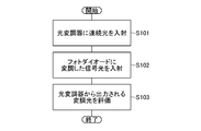
- FIG. 2 is a flowchart for explaining an optical inspection method according to an embodiment of the present invention.
- FIG. 3 is a characteristic diagram showing a measurement result of a voltage of an electric signal output by the photodiode 103 with respect to the power of light input to the photodiode 103.
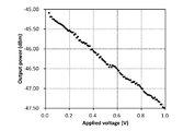
- FIG. 4 is a characteristic diagram showing the result of measuring the relationship between the voltage of the electric signal input (applied) to the light modulator 102 and the light modulated and output by the light modulator 102.
- FIG. 1 is a configuration diagram showing a configuration of an optical inspection circuit according to an embodiment of the present invention.
- FIG. 2 is a flowchart for explaining an optical inspection method according to an embodiment of the present invention.
- FIG. 3 is a characteristic diagram showing a measurement result of a voltage of an electric signal output by the photodiode 103 with respect to the power of light input to the photodi
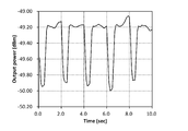
- FIG. 5 shows the optical output waveform of the modulated light output from the light modulator 102 as a result of inputting an optical pulse of 1 mW at peak power to the photodiode 103 connected to the light modulator 102 by wiring 107. It is a characteristic diagram.
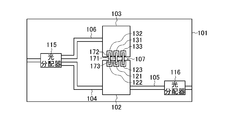
- FIG. 6 is a configuration diagram showing the configuration of another optical inspection circuit according to the embodiment of the present invention.
- FIG. 7 is a configuration diagram showing the configuration of another optical inspection circuit according to the embodiment of the present invention.
- FIG. 8 is a configuration diagram showing the configuration of another optical inspection circuit according to the embodiment of the present invention.
- This optical inspection circuit includes an optical modulator 102 formed on the substrate 101 and a photodiode 103 formed on the substrate 101 in the vicinity of the optical modulator 102.
- the light modulator 102 is composed of an optical waveguide, and the optical waveguide has a core made of a semiconductor.
- the light modulator 102 can be composed of, for example, a Machzenda optical modulator in which a carrier extraction type phase shifter having a pn junction formed in a rib-type optical waveguide having a silicon core and a multimode interferometer are combined.
- This light modulator can be manufactured by known semiconductor device manufacturing techniques such as widely known lithography techniques, ion implantation techniques, thin film deposition techniques, crystal growth techniques, and etching techniques.
- the photodiode 103 is a germanium photodiode composed of, for example, a layer of germanium selectively formed on a core made of a semiconductor (for example, silicon) and pn junctions formed on both sides of this layer and above and below the layer. Is.
- the photodiode 103 can be manufactured by known semiconductor device manufacturing techniques such as widely known lithography techniques, ion implantation techniques, thin film deposition techniques, crystal growth techniques, and etching techniques.
- a first optical waveguide 104 composed of an optical waveguide having a core made of a semiconductor is optically connected to the light modulator 102 as an input waveguide.
- a second optical waveguide 105 composed of an optical waveguide having a core made of a semiconductor is optically connected to the light modulator 102 as an output waveguide.
- a third optical waveguide 106 composed of an optical waveguide having a core made of a semiconductor is optically connected to the photodiode 103 as an input waveguide.
- the light modulator 102 and the photodiode 103 are electrically connected by wiring 107.
- the electric signal that is photoelectrically converted by the photodiode 103 and output is transmitted by the wiring 107 and input to the light modulator 102.
- the light modulator 102 modulates the continuous light input via the first optical waveguide 104 by the electric signal input via the wiring 107, and outputs the continuous light to the second optical waveguide 105.
- the wiring 107 is a high-frequency line composed of signal lines 171 and ground lines 172 and 173.
- the signal line 171 connects the electrode pad 121 of the light modulator 102 and the electrode pad 131 of the photodiode 103.
- the ground wire 172 connects the electrode pad 122 of the light modulator 102 and the electrode pad 132 of the photodiode 103.
- the ground wire 173 connects the electrode pad 123 of the light modulator 102 and the electrode pad 133 of the photodiode 103.
- optical modulator 110 is optically connected to the third optical waveguide 106 via the optical fiber 109.
- the light modulator 110 modulates the continuous light emitted from the light source 111 and outputs it to the optical fiber 109.
- the light source 111 is composed of, for example, a semiconductor laser.
- optical fiber 112 is optically connected to the first optical waveguide 104, and the continuous light emitted from the light source 113 is input to the optical fiber 112.
- the light source 113 is composed of, for example, a semiconductor laser.
- the modulated light (signal light) emitted from the light source 111 and modulated by the light modulator 110 is received by the photodiode 103 via the optical fiber 109 and the third optical waveguide 106.
- the modulated light received by the photodiode 103 is photoelectrically converted into a modulated electrical signal and output to the light modulator 102 via the wiring 107.
- the continuous light emitted from the light source 113 is input to the light modulator 102 via the optical fiber 112 and the first optical waveguide 104.
- the continuous light input to the light modulator 102 is modulated by the light modulator 102 driven by the input modulated electrical signal, output from the second optical waveguide 105, and taken out by the optical fiber 114.
- the optical inspection method according to the embodiment of the present invention will be described with reference to FIG.
- the continuous light emitted from the light source 113 is incident on the light modulator 102 via the first optical waveguide 104.
- the modulated light modulated by the light modulator 110 is incident on the photodiode 103.
- the modulated electrical signal is output to the light modulator 102 from the photodiode 103 to which the modulated light is incident.
- the light modulator 102 modulates and outputs the input continuous light with the modulated electrical signal received from the photodiode 103.
- the modulated light output from the light modulator 102 is evaluated.
- evaluation such as comparing the modulated light output from the light modulator 102 and taken out by the optical fiber 114 with the modulated light output from the light modulator 110 (input to the photodiode 103), at the wafer level.
- the light modulator 102 can be inspected.
- a probe card having excellent high frequency characteristics and a high frequency cable for connecting the probe card outside the wafer and the device on the wafer are not required, and the probe card is not required at the wafer level.
- the optical modulator 102 of the above can be inspected.
- the voltage of the electric signal output by the photodiode 103 when the voltage of the electric signal output by the photodiode 103 is measured with respect to the power of light input to the photodiode 103, the voltage changes as shown in FIG. As shown in FIG. 3, when light of about 1 mW is input to the photodiode 103, a voltage of about 0.15 V is generated.
- FIG. 4 shows the result of measuring the relationship between the voltage of the electric signal input (applied) to the light modulator 102 and the light output from the light modulator 102.
- FIG. 4 shows the result of measuring the relationship between the voltage of the electric signal input (applied) to the light modulator 102 and the light output from the light modulator 102.
- an electric signal having a voltage of about 0.2 V is applied to the light modulator 102, it can be seen that the output light has a change of about 0.5 dB.
- an optical pulse (modulated light) of 1 mW at peak power is input to the photodiode 103 connected to the light modulator 102 by wiring 107, and as a result, the optical output of the modulated light output from the light modulator 102.
- the waveform is shown in FIG.
- an optical modulation signal of about 0.5 dB is output, and the characteristic inspection of the light modulator 102 is possible by the optical inspection circuit according to the present embodiment. Is shown.
- This optical inspection circuit includes an optical modulator 102 formed on the substrate 101 and a photodiode 103 formed on the substrate 101 in the vicinity of the optical modulator 102. Further, the first optical waveguide 104 and the second optical waveguide 105 are optically connected to the light modulator 102. Further, a third optical waveguide 106 is optically connected to the photodiode 103. Further, the light modulator 102 and the photodiode 103 are electrically connected by wiring 107. These configurations are similar to the optical inspection circuit described with reference to FIG.
- This optical inspection circuit further includes an optical distributor 115 that distributes the input signal light to the first optical waveguide 104 and the third optical waveguide 106. Further, the wavelength filter 116 that extracts light having a predetermined wavelength from the light output from the light modulator 102 is provided. The light distributor 115 and the wavelength filter 116 are formed on the substrate 101. Further, the optical distributor 115 and the wavelength filter 116 are composed of an optical waveguide having a core made of a semiconductor.
- the optical distributor 115 distributes the input optical power to a plurality of optical waveguides, and can be composed of, for example, a Y-branch circuit.
- the optical distributor 115 can also be composed of a multimode interferometer.
- the optical distributor 115 can also be composed of a directional coupler.
- the wavelength filter 116 can be composed of a wavelength-dependent two-output optical circuit.
- the wavelength filter 116 can be composed of, for example, an array diffraction grating, an asymmetric Mach-Zehnder interferometer, a directional coupler, and the like.
- this optical inspection circuit continuous light and modulated light are combined and input to the optical distributor 115.
- the light distributor 115 the combined continuous light and the modulated light are distributed. Therefore, the combined continuous light and the modulated light are input to both the light modulator 102 and the photodiode 103.
- the light modulator 102 modulates the input light using the modulated electrical signal generated by the photodiode 103 with the modulated light in the combined light.
- the combined continuous light and the modulated light are input to the light modulator 102, of which the continuous light is the modulation target and the modulated light becomes noise.
- the light that becomes noise is removed by the wavelength filter 116.
- This optical inspection circuit has an excellent effect that the number of optical waveguides for input can be reduced to one.
- This optical inspection circuit comprises a plurality of optical modulators 102a, 102b, 102c formed on the substrate 101 and a photodiode 103 formed on the substrate 101 in the vicinity of the optical modulators 102a, 102b, 102c. Be prepared.
- the first optical waveguide 104a and the second optical waveguide 105a are optically connected to the light modulator 102a.
- a first optical waveguide 104b and a second optical waveguide 105b are optically connected to the light modulator 102b.
- a first optical waveguide 104c and a second optical waveguide 105c are optically connected to the light modulator 102c.
- a third optical waveguide 106 is optically connected to the photodiode 103.
- each of the light modulators 102a, 102b, 102c and the photodiode 103 are electrically connected by wiring 107a.
- the wiring 107a can be formed by, for example, wire bonding. Further, the wiring 107a can also be configured by a known multilayer wiring structure formed on the surface layer of the substrate 101.
- This optical inspection circuit has an excellent effect of being able to inspect a plurality of optical modulators 102a, 102b, 102c with a modulated electric signal generated from one photodiode 103.
- This optical inspection circuit includes an optical modulator 102 formed on the substrate 101, and a plurality of photodiodes 103a, 103b, 103c formed on the substrate 101 in the vicinity of the optical modulator 102.
- first optical waveguide 104 and the second optical waveguide 105 are optically connected to the light modulator 102.
- a third optical waveguide 106a is optically connected to the photodiode 103a.
- the third optical waveguide 106b is optically connected to the photodiode 103b.
- the third optical waveguide 106c is optically connected to the photodiode 103c.
- the light modulator 102 and the photodiode 103 are electrically connected by wiring 107b.
- the plurality of photodiodes 103a, 103b, 103c are connected in series to the light modulator 102 by wiring 107b.
- the wiring 107b can be formed by, for example, wire bonding. Further, the wiring 107b can also be configured by a known multilayer wiring structure formed on the surface layer of the substrate 101. According to this optical inspection circuit, by using a plurality of photodiodes 103a, 103b, 103c, a modulated electric signal having a larger voltage can be generated, and a large voltage is required among the modulation characteristics of the light modulator 102. It has the excellent effect of enabling property inspection.
- a photodiode is formed on a substrate on which an optical modulator is formed, and these are electrically connected by wiring, so that an optical circuit such as an optical modulator can be used. Wafer level inspections will be easier and cheaper to carry out.
Landscapes
- Physics & Mathematics (AREA)
- General Physics & Mathematics (AREA)
- Nonlinear Science (AREA)
- Optics & Photonics (AREA)
- Chemical & Material Sciences (AREA)
- Analytical Chemistry (AREA)
- Optical Modulation, Optical Deflection, Nonlinear Optics, Optical Demodulation, Optical Logic Elements (AREA)
- Light Receiving Elements (AREA)
- Testing Of Optical Devices Or Fibers (AREA)
Abstract
基板(101)の上に形成された光変調器(102)と、光変調器(102)の近傍の基板(101)の上に形成されたフォトダイオード(103)とを備える。また、光変調器(102)には、第1光導波路(104)が、入力導波路として光学的に接続している。また、光変調器(102)には、第2光導波路(105)が、出力導波路として光学的に接続している。また、フォトダイオード(103)には、第3光導波路(106)が、入力導波路として光学的に接続している。また、光変調器(102)とフォトダイオード(103)とは、配線(107)により電気的に接続している。
Description
本発明は、光回路の検査を行うための光検査回路および光検査方法に関する。
シリコンフォトニクス技術は、将来の光デバイスの低コスト化に向けた基盤技術として期待されている。しかし、真に低コスト化を実現するためには、光モジュール組み立て・検査コストの低減が求められる。特に、検査コストの削減のためには、多数のチップを短時間で測定可能なウエハレベル検査が必要になる。
光デバイスのウエハレベル検査技術に関する提案はいくつかあるが(非特許文献1,2,3)、光変調器のようなアクティブデバイスに適用可能な技術は少ない。これは光変調器が、電気信号を光信号に変換するデバイスであり、一般的に求められる応答速度が10ギガヘルツ以上と高速であることに起因する。
Y. Maeda et al., "Novel fiber alignment method for on-wafer testing of silicon photonic devices with PN junction embedded grating couplers", 2018 IEEE 15th International Conference on Group IV Photonics, 18162636, pp. 81-82, 2018.
T. Miura et al., "Novel quick and precise method for evaluating optical characteristics", 2018 IEEE 15th International Conference on Group IV Photonics, 18162651, pp. 95-96, 2018.
H. Fukuda et al., "Estimation of Optical Modulator Efficiency From Electrical Characteristics", 2018 IEEE 15th International Conference on Group IV Photonics, 18162656, pp. 11-12, 2018.
前述したように、光変調器のようなアクティブデバイスのウエハレベル検査では、求められる応答速度が10ギガヘルツ以上と高速であるため、高速電気信号を損失無く伝送する線路が要求される。高速電気信号を損失無く伝送する線路をウエハレベル検査に適用するためには、高周波特性に優れたプローブカードが必要になる。しかしながら、この種のプローブカードや、プローブカードとウエハ上の検査対象のデバイスとを接続する高周波ケーブルは、高価である。加えて、再現性の高い検査のためには、プローブカードと高周波ケーブルの取りまわしに細心の注意を払う必要があり、検査が容易に実施できず、量産工程では受け入れにくい。
本発明は、以上のような問題点を解消するためになされたものであり、光変調器などの光回路のウエハレベルの検査が、より容易に、より安価に実施できるようにすることを目的とする。
本発明に係る光検査回路は、基板の上に形成された光導波路から構成され、光導波路は半導体からなるコアを有する光変調器と、半導体からなるコアを有する光導波路から構成されて、光変調器に光学的接続する第1光導波路と、半導体からなるコアを有する光導波路から構成されて、光変調器に光学的接続する第2光導波路と、光変調器の近傍の基板の上に形成されたフォトダイオードと、光変調器とフォトダイオードとを電気的に接続する配線と、半導体からなるコアを有する光導波路から構成されて、フォトダイオードに光学的接続する第3光導波路とを備える。
上記光検査回路一構成例において、光変調器が複数形成され、配線は、複数の光変調器の各々と、フォトダイオードとを接続する。
上記光検査回路一構成例において、フォトダイオードが複数形成され、配線は、光変調器と、複数のフォトダイオードの各々とを接続する。
上記光検査回路一構成例において、入力される信号光を、第1光導波路と第3光導波路とに分配する光分配器をさらに備える。
上記光検査回路一構成例において、半導体は、シリコンであり、フォトダイオードは、ゲルマニウムフォトダイオードである。
本発明に係る光検査方法は、基板の上に形成された光導波路から構成され、光導波路は半導体からなるコアを有する光変調器に、連続光を入射する第1ステップと、光変調器の近傍の基板の上に形成されて光変調器と電気的に接続するフォトダイオードに、変調した信号光を入射する第2ステップと、光変調器より出力される変調光を評価する第3ステップとを備える。
以上説明したように、本発明によれば、光変調器が形成されている基板の上にフォトダイオードを形成し、これらを配線により電気的に接続したので、光変調器などの光回路のウエハレベルの検査が、より容易に、より安価に実施できる。
以下、本発明の実施の形態に係る光検査回路について図1を参照して説明する。この光検査回路は、基板101の上に形成された光変調器102と、光変調器102の近傍の基板101の上に形成されたフォトダイオード103とを備える。
光変調器102は、光導波路から構成され、光導波路は半導体からなるコアを有する。光変調器102は、例えばシリコンをコアとするリブ型光導波路に形成されたpn接合を備えるキャリア引き抜き型位相シフタと、マルチモード干渉計とを組み合わせたマッハツェンダ光変調器から構成することができる。この光変調器は、広く知られたリソグラフィ技術、イオン注入技術、薄膜堆積技術、結晶成長技術、およびエッチング技術など、公知の半導体装置の製造技術により製造可能である。
フォトダイオード103は、例えば、半導体(例えばシリコン)からなるコアの上に選択的に形成されたゲルマニウムの層と、この層の両側方、上下に形成されたpn接合とから構成されたゲルマニウムフォトダイオードである。フォトダイオード103は、広く知られたリソグラフィ技術、イオン注入技術、薄膜堆積技術、結晶成長技術、およびエッチング技術など、公知の半導体装置の製造技術により製造可能である。
また、光変調器102には、半導体からなるコアを有する光導波路から構成された第1光導波路104が、入力導波路として光学的に接続している。また、光変調器102には、半導体からなるコアを有する光導波路から構成された第2光導波路105が、出力導波路として光学的に接続している。また、フォトダイオード103には、半導体からなるコアを有する光導波路から構成された第3光導波路106が、入力導波路として光学的に接続している。
また、光変調器102とフォトダイオード103とは、配線107により電気的に接続している。フォトダイオード103で光電変換されて出力される電気信号が、配線107により電送され、光変調器102に入力される。光変調器102では、配線107を介して入力された電気信号により、第1光導波路104を介して入力された連続光を変調し、第2光導波路105に出力する。
例えば、配線107は、信号線171,接地線172,173から構成された高周波線路である。信号線171は、光変調器102の電極パッド121と、フォトダイオード103の電極パッド131とを接続する。接地線172は、光変調器102の電極パッド122と、フォトダイオード103の電極パッド132とを接続する。接地線173は、光変調器102の電極パッド123と、フォトダイオード103の電極パッド133とを接続する。
また、第3光導波路106には、光ファイバ109を介して光変調器110が光学的に接続している。光変調器110は、光源111から出射された連続光を変調し、光ファイバ109に出力する。光源111は、例えば、半導体レーザから構成されている。
また、第1光導波路104には、光ファイバ112が光学的に接続され、光ファイバ112には、光源113から出射された連続光が入力される。光源113は、例えば、半導体レーザから構成されている。
この光検査回路では、まず、光源111から出射されて光変調器110で変調された変調光(信号光)は、光ファイバ109,第3光導波路106を介してフォトダイオード103で受光される。フォトダイオード103で受光された変調光は、変調電気信号に光電変換されて、配線107を介して光変調器102に出力される。
また、光源113から出射された連続光は、光ファイバ112、第1光導波路104を介して光変調器102に入力される。光変調器102に入力した連続光は、入力される変調電気信号で駆動される光変調器102で変調され、第2光導波路105から出力され、光ファイバ114により取り出される。
以下、本発明の実施の形態に係る光検査方法について、図2を参照して説明する。まず、第1ステップS101で、光変調器102に、第1光導波路104を介し、光源113から出射された連続光を入射する。次に、第2ステップS102で、フォトダイオード103に、光変調器110で変調された変調光を入射する。前述したように、変調光が入射されたフォトダイオード103から、変調電気信号が光変調器102に出力される。光変調器102では、フォトダイオード103より受け付けた変調電気信号で、入力された連続光を変調して出力する。
この後、第3ステップS103で、光変調器102より出力される変調光を評価する。光変調器102より出力されて光ファイバ114で取り出された変調光を、光変調器110から出力される(フォトダイオード103に入力される)変調光と比較するなどの評価により、ウエハレベルでの光変調器102の検査が実施できる。
以上に説明したように、本実施の形態によれば、高周波特性に優れたプローブカードや、ウエハ外のプローブカードとウエハ上のデバイスとを接続するための高周波ケーブルを必要とせず、ウエハレベルでの光変調器102の検査が実施できる。
例えば、フォトダイオード103に入力された光のパワーに対し、フォトダイオード103が出力する電気信号の電圧を測定すると、図3に示すように変化する。図3に示されているように、フォトダイオード103に1mW程度の光が入力すると、0.15V程度の電圧を発生する。
一方、光変調器102に対して入力(印加)された電気信号の電圧と、光変調器102から出力される光との関係を測定した結果を図4に示す。図4に示されているように、光変調器102に0.2V程度の電圧の電気信号が印加されると、出力される光では、0.5dB程度の変化があることがわかる。
次に、光変調器102に配線107で接続されたフォトダイオード103に、ピークパワーで1mWの光パルス(変調光)を入力し、この結果として光変調器102から出力された変調光の光出力波形を図5に示す。図3,図4の結果から予測されるように、0.5dB程度の光変調信号を出力しており、本実施の形態に係る光検査回路により、光変調器102の特性検査が可能であることが示されている。
次に、本発明の実施の形態に係る他の光検査回路について、図6を参照して説明する。この光検査回路は、基板101の上に形成された光変調器102と、光変調器102の近傍の基板101の上に形成されたフォトダイオード103とを備える。また、光変調器102には、第1光導波路104および第2光導波路105が光学的に接続している。また、フォトダイオード103には、第3光導波路106が、光学的に接続している。また、光変調器102とフォトダイオード103とは、配線107により電気的に接続している。これらの構成は、図1を用いて説明した光検査回路と同様である。
この光検査回路は、さらに、入力される信号光を、第1光導波路104と第3光導波路106とに分配する光分配器115を備える。また、光変調器102から出力される光より所定の波長の光を取り出す波長フィルタ116を備える。光分配器115、波長フィルタ116は、基板101の上に形成されている。また、光分配器115、波長フィルタ116は、半導体からなるコアを有する光導波路から構成されている。
光分配器115は、入力される光パワーを、複数の光導波路へ分配するものであり、例えば、Y分岐回路から構成することができる。また、光分配器115は、マルチモード干渉計から構成することもできる。また、光分配器115は、方向性結合器から構成することもできる。波長フィルタ116は、波長依存性のある2出力光回路から構成することができる。波長フィルタ116は、例えば、アレイ回折格子、非対称マッハツェンダ干渉計、方向性結合器などから構成することができる。
この光検査回路では、光分配器115に、連続光と変調光とを合波して入力する。光分配器115では、合波された連続光と変調光とが分配される。従って、光変調器102およびフォトダイオード103の両者に、合波された連続光と変調光とが入力される。この構成では、合波された光の中の変調光によりフォトダイオード103で生成される変調電気信号を用い、光変調器102が、入力される光を変調する。光変調器102には、合波された連続光と変調光とが入力され、このうち、連続光が変調対象となり、変調光はノイズとなる。この、ノイズとなる光を波長フィルタ116で除去する。この光検査回路は、入力用光導波路を1つに削減できるという優れた効果を持つ。
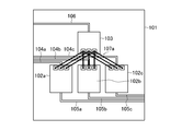
次に、本発明の実施の形態に係る他の光検査回路について、図7を参照して説明する。この光検査回路は、基板101の上に形成された複数の光変調器102a,102b,102cと、光変調器102a,102b,102cの近傍の基板101の上に形成されたフォトダイオード103とを備える。
光変調器102aには、第1光導波路104aおよび第2光導波路105aが光学的に接続している。光変調器102bには、第1光導波路104bおよび第2光導波路105bが光学的に接続している。光変調器102cには、第1光導波路104cおよび第2光導波路105cが光学的に接続している。また、フォトダイオード103には、第3光導波路106が光学的に接続している。
また、光変調器102a,102b,102cの各々とフォトダイオード103とは、配線107aにより電気的に接続している。配線107aは、例えば、ワイヤボンディングにより形成できる。また、配線107aは、基板101の表層に形成した公知の多層配線構造により構成することもできる。
この光検査回路は、1つのフォトダイオード103から生成された変調電気信号で、複数の光変調器102a,102b,102cを検査できるという優れた効果を持つ。
次に、本発明の実施の形態に係る他の光検査回路について、図8を参照して説明する。 この光検査回路は、基板101の上に形成された光変調器102と、光変調器102の近傍の基板101の上に形成された、複数のフォトダイオード103a,103b,103cとを備える。
また、光変調器102には、第1光導波路104および第2光導波路105が光学的に接続している。また、フォトダイオード103aには、第3光導波路106aが、光学的に接続している。また、フォトダイオード103bには、第3光導波路106bが、光学的に接続している。また、フォトダイオード103cには、第3光導波路106cが、光学的に接続している。
また、光変調器102とフォトダイオード103とは、配線107bにより電気的に接続している。複数のフォトダイオード103a,103b,103cは、配線107bにより、光変調器102に直列接続している。配線107bは、例えば、ワイヤボンディングにより形成できる。また、配線107bは、基板101の表層に形成した公知の多層配線構造により構成することもできる。この光検査回路によれば、複数のフォトダイオード103a,103b,103cを用いることで、より大きな電圧の変調電気信号が生成でき、光変調器102の変調特性の中で、大電圧を必要とする特性の検査が可能になるという優れた効果を持つ。
以上に説明したように、本発明によれば、光変調器が形成されている基板の上にフォトダイオードを形成し、これらを配線により電気的に接続したので、光変調器などの光回路のウエハレベルの検査が、より容易に、より安価に実施できるようになる。
なお、本発明は以上に説明した実施の形態に限定されるものではなく、本発明の技術的思想内で、当分野において通常の知識を有する者により、多くの変形および組み合わせが実施可能であることは明白である。
101…基板、102…光変調器、103…フォトダイオード、104…第1光導波路、105…第2光導波路、106…第3光導波路、107…配線、109…光ファイバ、110…光変調器、111…光源、112…光ファイバ、113…光源、114…光ファイバ、121,122,123…電極パッド、131,132,133…電極パッド、171…信号線、172,173…接地線。
Claims (6)
- 基板の上に形成された光導波路から構成され、前記光導波路は半導体からなるコアを有する光変調器と、
前記半導体からなるコアを有する光導波路から構成されて、前記光変調器に光学的接続する第1光導波路と、
前記半導体からなるコアを有する光導波路から構成されて、前記光変調器に光学的接続する第2光導波路と、
前記光変調器の近傍の前記基板の上に形成されたフォトダイオードと、
前記光変調器と前記フォトダイオードとを電気的に接続する配線と、
前記半導体からなるコアを有する光導波路から構成されて、前記フォトダイオードに光学的接続する第3光導波路と
を備える光検査回路。 - 請求項1記載の光検査回路において、
前記光変調器が複数形成され、
前記配線は、前記複数の光変調器の各々と、前記フォトダイオードとを接続する
ことを特徴とする光検査回路。 - 請求項1または2記載の光検査回路において、
前記フォトダイオードが複数形成され、
前記配線は、前記光変調器と、前記複数のフォトダイオードの各々とを接続する
ことを特徴とする光検査回路。 - 請求項1~3のいずれか1項に記載の光検査回路において、
入力される信号光を、前記第1光導波路と前記第3光導波路とに分配する光分配器をさらに備えることを特徴とする光検査回路。 - 請求項1~4のいずれか1項に記載の光検査回路において、
前記半導体は、シリコンであり、
前記フォトダイオードは、ゲルマニウムフォトダイオードである
ことを特徴とする光検査回路。 - 基板の上に形成された光導波路から構成され、前記光導波路は半導体からなるコアを有する光変調器に、連続光を入射する第1ステップと、
前記光変調器の近傍の前記基板の上に形成されて前記光変調器と電気的に接続するフォトダイオードに、変調した信号光を入射する第2ステップと、
前記光変調器より出力される変調光を評価する第3ステップと
を備える光検査方法。
Priority Applications (3)
| Application Number | Priority Date | Filing Date | Title |
|---|---|---|---|
| JP2021520009A JP7143948B2 (ja) | 2019-05-23 | 2019-05-23 | 光検査回路および光検査方法 |
| PCT/JP2019/020473 WO2020235083A1 (ja) | 2019-05-23 | 2019-05-23 | 光検査回路および光検査方法 |
| US17/609,092 US12197051B2 (en) | 2019-05-23 | 2019-05-23 | Optical inspection circuit and optical inspection method |
Applications Claiming Priority (1)
| Application Number | Priority Date | Filing Date | Title |
|---|---|---|---|
| PCT/JP2019/020473 WO2020235083A1 (ja) | 2019-05-23 | 2019-05-23 | 光検査回路および光検査方法 |
Publications (1)
| Publication Number | Publication Date |
|---|---|
| WO2020235083A1 true WO2020235083A1 (ja) | 2020-11-26 |
Family
ID=73458425
Family Applications (1)
| Application Number | Title | Priority Date | Filing Date |
|---|---|---|---|
| PCT/JP2019/020473 Ceased WO2020235083A1 (ja) | 2019-05-23 | 2019-05-23 | 光検査回路および光検査方法 |
Country Status (3)
| Country | Link |
|---|---|
| US (1) | US12197051B2 (ja) |
| JP (1) | JP7143948B2 (ja) |
| WO (1) | WO2020235083A1 (ja) |
Cited By (1)
| Publication number | Priority date | Publication date | Assignee | Title |
|---|---|---|---|---|
| WO2024116388A1 (ja) * | 2022-12-01 | 2024-06-06 | 日本電信電話株式会社 | 光回路の測定回路、光回路の測定方法 |
Citations (5)
| Publication number | Priority date | Publication date | Assignee | Title |
|---|---|---|---|---|
| WO2014034238A1 (ja) * | 2012-08-29 | 2014-03-06 | 日本電気株式会社 | 光集積回路、および光集積回路における光デバイスの検査方法 |
| JP2015191068A (ja) * | 2014-03-27 | 2015-11-02 | 日本電気株式会社 | 光変調器の出力モニター方法および出力モニター装置 |
| CN106411399A (zh) * | 2016-08-31 | 2017-02-15 | 武汉光迅科技股份有限公司 | 双并联mzi型电光调制器光学损耗的自动测试方法与装置 |
| JP2019045749A (ja) * | 2017-09-05 | 2019-03-22 | 日本電信電話株式会社 | 光回路 |
| JP2019096763A (ja) * | 2017-11-24 | 2019-06-20 | 日本電信電話株式会社 | 光特性検査用回路 |
Family Cites Families (2)
| Publication number | Priority date | Publication date | Assignee | Title |
|---|---|---|---|---|
| KR100794416B1 (ko) | 2006-04-13 | 2008-01-16 | 포스데이타 주식회사 | SIP를 기반으로 하는 VoIP 호에 대한 패킷 과금정보의 획득 방법 |
| US10476600B2 (en) * | 2018-01-12 | 2019-11-12 | Sicoya Gmbh | Optical signal modulator comprising a feedback-loop |
-
2019
- 2019-05-23 WO PCT/JP2019/020473 patent/WO2020235083A1/ja not_active Ceased
- 2019-05-23 JP JP2021520009A patent/JP7143948B2/ja active Active
- 2019-05-23 US US17/609,092 patent/US12197051B2/en active Active
Patent Citations (5)
| Publication number | Priority date | Publication date | Assignee | Title |
|---|---|---|---|---|
| WO2014034238A1 (ja) * | 2012-08-29 | 2014-03-06 | 日本電気株式会社 | 光集積回路、および光集積回路における光デバイスの検査方法 |
| JP2015191068A (ja) * | 2014-03-27 | 2015-11-02 | 日本電気株式会社 | 光変調器の出力モニター方法および出力モニター装置 |
| CN106411399A (zh) * | 2016-08-31 | 2017-02-15 | 武汉光迅科技股份有限公司 | 双并联mzi型电光调制器光学损耗的自动测试方法与装置 |
| JP2019045749A (ja) * | 2017-09-05 | 2019-03-22 | 日本電信電話株式会社 | 光回路 |
| JP2019096763A (ja) * | 2017-11-24 | 2019-06-20 | 日本電信電話株式会社 | 光特性検査用回路 |
Cited By (1)
| Publication number | Priority date | Publication date | Assignee | Title |
|---|---|---|---|---|
| WO2024116388A1 (ja) * | 2022-12-01 | 2024-06-06 | 日本電信電話株式会社 | 光回路の測定回路、光回路の測定方法 |
Also Published As
| Publication number | Publication date |
|---|---|
| JPWO2020235083A1 (ja) | 2020-11-26 |
| US12197051B2 (en) | 2025-01-14 |
| US20220229317A1 (en) | 2022-07-21 |
| JP7143948B2 (ja) | 2022-09-29 |
Similar Documents
| Publication | Publication Date | Title |
|---|---|---|
| JP7202312B2 (ja) | ウエハのプローブおよび検査を可能にするシリコンフォトニクス構造 | |
| CN111123447B (zh) | 光收发器、使用其的光收发器模块及光收发器的测试方法 | |
| US10145758B2 (en) | Wafer level optical probing structures for silicon photonics | |
| Liu et al. | Wavelength division multiplexing based photonic integrated circuits on silicon-on-insulator platform | |
| US8311374B2 (en) | Beam generation and steering with integrated optical circuits for light detection and ranging | |
| US20100040322A1 (en) | Integrated electro-optic device and method of making | |
| US11815422B2 (en) | Optical test circuit | |
| CN113366283B (zh) | 用于全光晶圆验收测试的方法和系统 | |
| JPWO2014112077A1 (ja) | 光配線チップとその検査方法、および光受信器 | |
| JP2019207305A (ja) | 光検査回路 | |
| CN209471277U (zh) | 光电芯片 | |
| Streshinsky et al. | Silicon parallel single mode 48× 50 gb/s modulator and photodetector array | |
| JP7143948B2 (ja) | 光検査回路および光検査方法 | |
| JP6823571B2 (ja) | 光回路 | |
| US20210208339A1 (en) | Optical Circuit for Alignment and Optical Alignment Method | |
| JP6915508B2 (ja) | 光回路の検査方法 | |
| TWI854408B (zh) | 一種測量馬赫-陳德爾調變器行進波的光電特性的方法及其裝置 | |
| Tartaret-Josnière et al. | Microwave photonics summation device with up to 19 input signals in k and ku bands | |
| Bœuf et al. | Silicon photonics research and manufacturing using a 300-mm wafer platform | |
| US12066665B2 (en) | Optical circuit for alignment and optical alignment method | |
| JP7643528B2 (ja) | 光特性検査用回路、装置および方法 | |
| Liu et al. | Silicon photonic integration for high-speed applications | |
| Dong et al. | Design of Photonic Integrated Phased Arrays |
Legal Events
| Date | Code | Title | Description |
|---|---|---|---|
| 121 | Ep: the epo has been informed by wipo that ep was designated in this application |
Ref document number: 19929796 Country of ref document: EP Kind code of ref document: A1 |
|
| ENP | Entry into the national phase |
Ref document number: 2021520009 Country of ref document: JP Kind code of ref document: A |
|
| NENP | Non-entry into the national phase |
Ref country code: DE |
|
| 122 | Ep: pct application non-entry in european phase |
Ref document number: 19929796 Country of ref document: EP Kind code of ref document: A1 |