WO2020230665A1 - 半導体記憶装置 - Google Patents
半導体記憶装置 Download PDFInfo
- Publication number
- WO2020230665A1 WO2020230665A1 PCT/JP2020/018392 JP2020018392W WO2020230665A1 WO 2020230665 A1 WO2020230665 A1 WO 2020230665A1 JP 2020018392 W JP2020018392 W JP 2020018392W WO 2020230665 A1 WO2020230665 A1 WO 2020230665A1
- Authority
- WO
- WIPO (PCT)
- Prior art keywords
- transistor
- wiring
- storage device
- local
- semiconductor storage
- Prior art date
- Legal status (The legal status is an assumption and is not a legal conclusion. Google has not performed a legal analysis and makes no representation as to the accuracy of the status listed.)
- Ceased
Links
Images


Classifications
-
- G—PHYSICS
- G11—INFORMATION STORAGE
- G11C—STATIC STORES
- G11C17/00—Read-only memories programmable only once; Semi-permanent stores, e.g. manually-replaceable information cards
- G11C17/08—Read-only memories programmable only once; Semi-permanent stores, e.g. manually-replaceable information cards using semiconductor devices, e.g. bipolar elements
- G11C17/10—Read-only memories programmable only once; Semi-permanent stores, e.g. manually-replaceable information cards using semiconductor devices, e.g. bipolar elements in which contents are determined during manufacturing by a predetermined arrangement of coupling elements, e.g. mask-programmable ROM
- G11C17/12—Read-only memories programmable only once; Semi-permanent stores, e.g. manually-replaceable information cards using semiconductor devices, e.g. bipolar elements in which contents are determined during manufacturing by a predetermined arrangement of coupling elements, e.g. mask-programmable ROM using field-effect devices
-
- G—PHYSICS
- G11—INFORMATION STORAGE
- G11C—STATIC STORES
- G11C11/00—Digital stores characterised by the use of particular electric or magnetic storage elements; Storage elements therefor
- G11C11/21—Digital stores characterised by the use of particular electric or magnetic storage elements; Storage elements therefor using electric elements
- G11C11/34—Digital stores characterised by the use of particular electric or magnetic storage elements; Storage elements therefor using electric elements using semiconductor devices
- G11C11/40—Digital stores characterised by the use of particular electric or magnetic storage elements; Storage elements therefor using electric elements using semiconductor devices using transistors
- G11C11/401—Digital stores characterised by the use of particular electric or magnetic storage elements; Storage elements therefor using electric elements using semiconductor devices using transistors forming cells needing refreshing or charge regeneration, i.e. dynamic cells
- G11C11/4063—Auxiliary circuits, e.g. for addressing, decoding, driving, writing, sensing or timing
- G11C11/407—Auxiliary circuits, e.g. for addressing, decoding, driving, writing, sensing or timing for memory cells of the field-effect type
- G11C11/4074—Power supply or voltage generation circuits, e.g. bias voltage generators, substrate voltage generators, back-up power, power control circuits
-
- G—PHYSICS
- G11—INFORMATION STORAGE
- G11C—STATIC STORES
- G11C11/00—Digital stores characterised by the use of particular electric or magnetic storage elements; Storage elements therefor
- G11C11/21—Digital stores characterised by the use of particular electric or magnetic storage elements; Storage elements therefor using electric elements
- G11C11/34—Digital stores characterised by the use of particular electric or magnetic storage elements; Storage elements therefor using electric elements using semiconductor devices
- G11C11/40—Digital stores characterised by the use of particular electric or magnetic storage elements; Storage elements therefor using electric elements using semiconductor devices using transistors
- G11C11/401—Digital stores characterised by the use of particular electric or magnetic storage elements; Storage elements therefor using electric elements using semiconductor devices using transistors forming cells needing refreshing or charge regeneration, i.e. dynamic cells
- G11C11/4063—Auxiliary circuits, e.g. for addressing, decoding, driving, writing, sensing or timing
- G11C11/407—Auxiliary circuits, e.g. for addressing, decoding, driving, writing, sensing or timing for memory cells of the field-effect type
- G11C11/408—Address circuits
- G11C11/4085—Word line control circuits, e.g. word line drivers, - boosters, - pull-up, - pull-down, - precharge
-
- G—PHYSICS
- G11—INFORMATION STORAGE
- G11C—STATIC STORES
- G11C11/00—Digital stores characterised by the use of particular electric or magnetic storage elements; Storage elements therefor
- G11C11/21—Digital stores characterised by the use of particular electric or magnetic storage elements; Storage elements therefor using electric elements
- G11C11/34—Digital stores characterised by the use of particular electric or magnetic storage elements; Storage elements therefor using electric elements using semiconductor devices
- G11C11/40—Digital stores characterised by the use of particular electric or magnetic storage elements; Storage elements therefor using electric elements using semiconductor devices using transistors
- G11C11/401—Digital stores characterised by the use of particular electric or magnetic storage elements; Storage elements therefor using electric elements using semiconductor devices using transistors forming cells needing refreshing or charge regeneration, i.e. dynamic cells
- G11C11/4063—Auxiliary circuits, e.g. for addressing, decoding, driving, writing, sensing or timing
- G11C11/407—Auxiliary circuits, e.g. for addressing, decoding, driving, writing, sensing or timing for memory cells of the field-effect type
- G11C11/409—Read-write [R-W] circuits
- G11C11/4094—Bit-line management or control circuits
-
- H—ELECTRICITY
- H10—SEMICONDUCTOR DEVICES; ELECTRIC SOLID-STATE DEVICES NOT OTHERWISE PROVIDED FOR
- H10B—ELECTRONIC MEMORY DEVICES
- H10B20/00—Read-only memory [ROM] devices
- H10B20/27—ROM only
- H10B20/30—ROM only having the source region and the drain region on the same level, e.g. lateral transistors
- H10B20/34—Source electrode or drain electrode programmed
-
- H—ELECTRICITY
- H10—SEMICONDUCTOR DEVICES; ELECTRIC SOLID-STATE DEVICES NOT OTHERWISE PROVIDED FOR
- H10B—ELECTRONIC MEMORY DEVICES
- H10B20/00—Read-only memory [ROM] devices
- H10B20/27—ROM only
- H10B20/50—ROM only having transistors on different levels, e.g. 3D ROM
-
- G—PHYSICS
- G11—INFORMATION STORAGE
- G11C—STATIC STORES
- G11C5/00—Details of stores covered by group G11C11/00
- G11C5/06—Arrangements for interconnecting storage elements electrically, e.g. by wiring
- G11C5/063—Voltage and signal distribution in integrated semi-conductor memory access lines, e.g. word-line, bit-line, cross-over resistance, propagation delay
Definitions
- the present disclosure relates to a semiconductor storage device using a CFET (Complementary FET) device, and more particularly to a layout structure of a mask ROM (Read Only Memory) using a CFET.
- CFET Complementary FET
- the mask ROM includes memory cells arranged in an array, and each memory cell is programmed and manufactured so as to have a fixed data state.
- the transistor constituting the memory cell is provided between the bit line and the VSS, and the word line is connected to the gate.
- Bit data "1" / "0" is stored depending on whether or not the source or drain is connected to the bit line or VSS.
- the presence or absence of connection is realized by, for example, the presence or absence of contacts or vias.
- the transistor which is a basic component of LSI, has realized improvement of integration degree, reduction of operating voltage, and improvement of operating speed by reducing (scaling) the gate length.
- off-current due to excessive scaling and the resulting significant increase in power consumption have become problems.
- three-dimensional structure transistors in which the transistor structure is changed from the conventional planar type to the three-dimensional type are being actively studied.
- Non-Patent Documents 1 and 2 disclose, as new devices, a three-dimensional structure device in which a three-dimensional structure P-type FET and an N-type FET are laminated in a direction perpendicular to a substrate, and a standard cell using the three-dimensional structure device.
- a three-dimensional structure device in which a three-dimensional structure P-type FET and an N-type FET are laminated in a direction perpendicular to a substrate is referred to as a CFET (Complementary FET), following the description of Non-Patent Document 1. To do. Further, the direction perpendicular to the substrate is called the depth direction.
- CFET Complementary FET
- An object of the present disclosure is to provide a layout structure of a mask ROM using a CFET.
- a semiconductor storage device including a ROM (Read Only Memory) memory cell, the word line extending in the first direction and the first extending in a second direction perpendicular to the first direction.
- the ROM memory cell is a three-dimensional transistor provided between the first bit wire and the ground power supply wiring, which includes a second bit wire and a ground power supply wiring extending in the second direction.
- a three-dimensional structure transistor provided between one transistor, the second bit wire, and the ground power supply wiring, which is formed on the upper layer of the first transistor and is viewed in plan from the first transistor.
- the second transistor on which the channel portion overlaps the first local wiring connected to the source of the first transistor and extending from the first transistor in the first direction in the first direction, and the source of the second transistor.
- a third local wiring extending in two directions and a fourth local wiring connected to the drain of the second transistor and extending from the second transistor in the direction opposite to the second direction in the first direction are provided.
- the gates of the first and second transistors are connected to the word line, and the ROM memory cell has the presence or absence of a connection between the first local wiring and the ground power supply wiring, or the third local wiring and the said.
- the first data is stored depending on the presence or absence of connection with the first bit line, and the presence or absence of connection between the second local wiring and the ground power supply wiring, or the fourth local wiring and the second bit line.
- the second data is stored depending on whether or not the transistor is connected.
- the ROM memory cell is provided between the first transistor, which is a three-dimensional structure transistor provided between the first bit wire and the ground power supply wiring, and between the second bit wire and the ground power supply wiring. It includes a second transistor which is a three-dimensional structure transistor. The second transistor is formed on the upper layer of the first transistor, and the channel portion overlaps with the first transistor in a plan view. Then, the ROM memory cell has a connection between the first local wiring connected to the source of the first transistor and the ground power supply wiring, or the third local wiring and the first bit line connected to the drain of the first transistor. The first data is stored depending on whether or not there is a connection with.
- the ROM memory cell has a connection between the second local wiring connected to the source of the second transistor and the ground power supply wiring, or the fourth local wiring and the second bit line connected to the drain of the second transistor.
- the second data is stored depending on whether or not there is a connection with. As a result, it is possible to realize a layout structure having a small area for the mask ROM.
- a second aspect of the present disclosure is a semiconductor integrated circuit device including a ROM (Read Only Memory) memory cell, in which a word line extending in the first direction and a bit extending in a second direction perpendicular to the first direction.
- the ROM memory cell includes a wire and a ground power supply wiring extending in the second direction, and the ROM memory cell is a first transistor and the bit, which are three-dimensional structure transistors provided between the bit wire and the ground power supply wiring.
- a second three-dimensional structure transistor provided between the wire and the ground power supply wiring, which is formed on the upper layer of the first transistor and whose channel portion overlaps with the first transistor in a plan view.
- the transistor the first local wiring connected to the source of the first transistor, the second local wiring connected to the source of the second transistor and connected to the first local wiring, and the first local wiring.
- the first and first local wirings include a third local wiring connected to the drain of one transistor and a fourth local wiring connected to the drain of the second transistor and connected to the third local wiring.
- the gate of the two transistors is connected to the word line, and the ROM memory cell has the presence or absence of connection between the first and second local wirings and the ground power supply wiring, or the third and fourth local wirings. Data is stored depending on whether or not there is a connection between the wire and the bit wire.
- the ROM memory cell includes first and second transistors which are three-dimensional structure transistors provided between the bit line and the ground power supply wiring.
- the second transistor is formed on the upper layer of the first transistor, and the channel portion overlaps with the first transistor in a plan view.
- the first local wiring connected to the source of the first transistor and the second local wiring connected to the source of the second transistor are connected to each other.
- the third local wiring connected to the drain of the first transistor and the fourth local wiring connected to the drain of the second transistor are connected to each other.
- the ROM memory cell stores data depending on whether or not the first and second local wirings are connected to the ground power supply wiring, or whether or not the third and fourth local wirings are connected to the bit wire. As a result, it is possible to realize a layout structure having a small area for the mask ROM.
- a third aspect of the present disclosure is a semiconductor storage device including a ROM (Read Only Memory) memory cell, wherein a word line extending in the first direction and a first direction extending in a second direction perpendicular to the first direction.
- the ROM memory cell is a three-dimensional transistor provided between the first bit line and the ground power supply wiring, and includes a second bit wire and a ground power supply wiring extending in the second direction.
- a solid provided between the first transistor, the second bit line, and the ground power supply wiring, which includes two transistors arranged in the second direction and sharing the first node, which is one of the source and drain.
- a structural transistor which includes two transistors that are arranged in the second direction and share the first node with each other, are formed on the upper layer of the first transistor, and are viewed in plan from the first transistor.
- Two third local wires connected to the second node of the transistor, which is the other of the source and drain, and extending in the second direction in the first direction, and the two transistors included in the second transistor.
- Each of the first and second transistors is connected to a second node and has two fourth local wirings extending in opposite directions to the second direction in the first direction, the first and second transistors having a gate connected to the word line.
- first data is stored depending on whether or not the first local wiring is connected to the ground power supply wiring or the first bit line, and the second local wiring and the grounding are performed.
- the second data is stored depending on whether or not it is connected to the power supply wiring or the second bit line.
- the ROM memory cell is provided between the first transistor, which is a three-dimensional structure transistor provided between the first bit wire and the ground power supply wiring, and between the second bit wire and the ground power supply wiring. It includes a second transistor which is a three-dimensional structure transistor. The second transistor is formed on the upper layer of the first transistor, and the channel portion overlaps with the first transistor in a plan view.
- the first and second transistors include two transistors that are aligned in the second direction in which the first and second bit wires and the grounded power supply wiring extend, respectively, and share the first node, which is one of the source and drain.
- the first data is stored depending on whether or not the first local wiring connected to the first node shared by the two transistors included in the first transistor is connected to the ground power supply wiring or the first bit line. It will be remembered. Further, in the ROM memory cell, the second data is stored depending on whether or not the second local wiring connected to the first node shared by the two transistors included in the second transistor is connected to the ground power supply wiring or the second bit line. It will be remembered. As a result, it is possible to realize a layout structure having a small area for the mask ROM.
- FIG. 2 and 3 are plan views which show the layout structure example of the memory cell which concerns on 1st Embodiment.
- A) to (c) are sectional views of the memory cell of FIG. It is a layout structure of the upper part of the memory cell array using the memory cells of FIGS. 2 and 3. It is a layout structure of the lower part of the memory cell array using the memory cells of FIGS. 2 and 3.
- A) and (b) are plan views which show an example of the layout structure of the inverter cell using CFET.
- A) and (b) are plan views showing another example of the layout structure of the memory cell according to the first embodiment.
- FIG. 1 A and (b) are plan views showing another example of the layout structure of the memory cell according to the first embodiment.
- (A) and (b) are plan views showing another example of the layout structure of the memory cell according to the first embodiment.
- FIG. 1 A layout structure of the upper part of the memory cell array using the memory cell of FIG.
- FIG. 1 A layout structure of the lower part of the memory cell array using the memory cell of FIG.
- FIG. 1 A layout structure and (b) are plan views which show another example of the layout structure of the memory cell which concerns on the modification of 1st Embodiment.
- FIGS. 16 and 17 are plan views which show another example of the layout structure of the memory cell which concerns on the modification of 1st Embodiment.
- FIGS. 16 and 17 are plan views which show another example of the layout structure of the memory cell which concerns on the modification of 1st Embodiment.
- FIGS. 16 and 17 are plan views which show the layout structure example of the memory cell which concerns on 2nd Embodiment.
- (A) to (c) are sectional views of the memory cell of FIG. It is a layout structure of the upper part of the memory cell array using the memory cells of FIGS. 16 and 17. It is a layout structure of the lower part of the memory cell array using the memory cells of FIGS. 16 and 17.
- (A) and (b) are plan views showing another example of the layout structure of the memory cell according to the second embodiment.
- (A) and (b) are plan views showing another example of the layout structure of the memory cell according to the second embodiment.
- (A) and (b) are plan views showing another example of the layout structure of the memory cell according to the second embodiment.
- (A) and (b) are plan views showing another example of the layout structure of the memory cell according to the second embodiment.
- (A) and (b) are plan views which show the layout structure example of the memory cell which concerns on 3rd Embodiment. It is a layout structure of the upper part of the memory cell array using the memory cell of FIG. 23. It is a layout structure of the lower part of the memory cell array using the memory cell of FIG. 23.
- (A) and (b) are plan views showing another example of the layout structure of the memory cell according to the third embodiment.
- FIGS. 29 and 30 are sectional views of the memory cell of FIG. 29. It is a layout structure of the upper part of the memory cell array using the memory cells of FIGS. 29 and 30. It is a layout structure of the lower part of the memory cell array using the memory cells of FIGS. 29 and 30.
- FIGS. 29 and 30 are plan views showing another example of the layout structure of the memory cell according to the fourth embodiment.
- FIGS. 1 and (b) are plan views which show another example of the layout structure of the memory cell which concerns on the modification of 4th Embodiment.
- Sectional drawing which shows the structure of the semiconductor device provided with CFET Sectional drawing which shows the structure of the semiconductor device provided with CFET Sectional drawing which shows the structure of the semiconductor device provided with CFET Top view showing the structure of the semiconductor device provided with CFET
- FIGS. 35 to 38 are views showing the structure of a semiconductor device provided with a CFET
- FIG. 35 is a sectional view in the X direction
- FIG. 36 is a sectional view of a gate portion in the Y direction
- FIG. 37 is a source / drain in the Y direction.
- FIG. 38 is a plan view.
- the X direction is the direction in which the nanowires extend
- the Y direction is the direction in which the gate extends
- the Z direction is the direction perpendicular to the substrate surface.
- FIGS. 35 to 38 are schematic views, and the dimensions and positions of the respective parts are not necessarily consistent.
- an element separation region 302 is formed on the surface of a semiconductor substrate 301 such as a silicon (Si) substrate, and the element active region 30a is defined by the element separation region 302.
- a semiconductor substrate 301 such as a silicon (Si) substrate
- the element active region 30a is defined by the element separation region 302.
- an N-type FET is formed on the P-type FET.
- a laminated transistor structure 390a is formed on the semiconductor substrate 301.
- the laminated transistor structure 390a includes a gate structure 391 formed on the semiconductor substrate 301.
- the gate structure 391 includes a gate electrode 356, a plurality of nanowires 358, a gate insulating film 355, and an insulating film 357.
- the gate electrode 356 extends in the Y direction and rises in the Z direction.
- the nanowires 358 penetrate the gate electrode 356 in the X direction and are arranged in the Y and Z directions.
- the gate insulating film 355 is formed between the gate electrode 356 and the nanowire 358.
- the gate electrode 356 and the gate insulating film 355 are formed at positions recessed from both ends of the nanowire 358 in the X direction, and the insulating film 357 is formed at the recessed portions.
- Insulating films 316 are formed on the semiconductor substrate 301 on both sides of the insulating film 357.
- Reference numerals 321 and 322 are interlayer insulating films.
- the gate electrode 356 is connected to the upper layer wiring by the via 385 provided in the opening 375.
- titanium, titanium nitride, polycrystalline silicon, or the like can be used for the gate electrode 356.
- a high dielectric constant material such as hafnium oxide, aluminum oxide, or oxides of hafnium and aluminum can be used for the gate insulating film 355.
- silicon or the like can be used for the nanowire 358.
- silicon oxide, silicon nitride, or the like can be used for the insulating film 316 and the insulating film 357.
- the number of nanowires 358 arranged in the Z direction is 4, and in the element active region 30a, a p-type semiconductor layer 331p is formed at each end of the two nanowires 358 on the semiconductor substrate 301 side. ..
- Two local wirings 386 in contact with the p-type semiconductor layer 331p are formed so as to sandwich the gate structure 391 in the X direction.
- an n-type semiconductor layer 341n is formed at each end of the two nanowires 358 on the side separated from the semiconductor substrate 101.
- Two local wirings 388 in contact with the n-type semiconductor layer 341n are formed so as to sandwich the gate structure 391 in the X direction.
- An insulating film 332 is formed between the local wiring 386 and the local wiring 388.
- An insulating film 389 is formed on the local wiring 388.
- the p-type semiconductor layer 331p is a p-type SiGe layer
- the n-type semiconductor layer 341n is an n-type Si layer.
- silicon oxide, silicon nitride, or the like can be used for the insulating film 332.
- the local wiring 388 is connected to the embedded wiring 3101 via the via 3071.
- the local wiring 386 is connected to the embedded wiring 3102 via the via 3072.
- the laminated transistor structure 390a has a P-type FET including a gate electrode 356, nanowires 358, a gate insulating film 355, and a P-type semiconductor layer 331p.
- a P-type FET including a gate electrode 356, nanowires 358, a gate insulating film 355, and a P-type semiconductor layer 331p.
- one P-type semiconductor layer 331p functions as a source region
- the other P-type semiconductor layer 331p functions as a drain region
- nanowire 358 functions as a channel.
- the laminated transistor structure 390a also has an N-type FET including a gate electrode 356, nanowires 358, a gate insulating film 355, and an N-type semiconductor layer 341n.
- one N-type semiconductor layer 341n functions as a source region
- the other N-type semiconductor layer 341n functions as a drain region
- nanowire 358 functions as a channel.
- wiring between transistors is performed by vias and metal wiring, but these can be realized by a known wiring process.
- the number of nanowires in the P-type FET and the N-type FET is assumed to be four in the Y direction and two in the Z direction, respectively, for a total of eight, but the number of nanowires is limited to this. It is not something that can be done. Further, the number of nanowires of the P-type FET and the N-type FET may be different.
- the semiconductor layer portion formed at both ends of the nanowire and forming the terminal serving as the source or drain of the transistor is referred to as a "pad".
- the p-type semiconductor layer 331p and the n-type semiconductor layer 341n correspond to pads.
- each insulating film and the like may be omitted.
- the nanowires and the pads on both sides thereof may be described in a simplified linear shape.
- expressions such as "same size” and the like that mean that the sizes and the like are the same include a range of manufacturing variation.
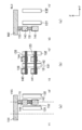
- FIG. 1 is a circuit diagram showing a configuration of a contact type mask ROM as an example of a semiconductor storage device.
- the contact-type mask ROM corresponds to "0" and "1" of the stored data depending on whether the drain of the memory cell transistor is connected to the bit line via the contact or not.
- the mask ROM includes a memory cell array 3, a column decoder 2, and a sense amplifier 18.
- the gates of the memory cells Mij are commonly connected to the word line WLi in the row direction, and their sources are connected to the ground potential VSS.
- the drain of the memory cell Mij is connected to the bit line BLj when the stored data is set to “0”, and is not connected to the bit line BLj when the stored data is set to “1”.
- the column decoder 2 is composed of an N-type MOS transistor Cj.
- the drains are all connected in common, the gate is connected to the column selection signal line CLj, and the source is connected to the bit line BLj.
- the sense amplifier 18 includes a P-type MOS transistor 5 for precharging, an inverter 8 for determining the output data of the memory cell Mij, and an inverter 9 for buffering the output signal of the inverter 8.
- a precharge signal NPR is input to the gate of the P-type MOS transistor 5, a power supply voltage VDD is supplied to the source, and the drain is connected to the common drain of the N-type MOS transistor Cj.
- the inverter 8 receives the signal SIN of the common drain of the N-type MOS transistor Cj and determines the output data of the memory cell Mij.
- the inverter 9 receives the output signal SOUT of the inverter 8 and outputs the stored data of the memory cell Mij.
- the operation of the mask ROM of FIG. 1 will be described by taking the case of reading the data of the memory cell M00 as an example.
- the precharge signal NPR is changed from high level to low level, and the precharge P-type MOS transistor 5 is turned on.
- the current capacity of the memory cell M00 is larger than that of the precharge P-type MOS transistor 5, so that the input signal SIN of the inverter 8 is the switching of the inverter 8.
- the voltage will be lower than the level. Therefore, the output signal SOUT of the inverter 8 holds the high level, and the output signal OUT of the inverter 9 holds the low level.
- the bit line BL0 is charged by the precharging P-type MOS transistor 5, and the input signal SIN of the inverter 8 is higher than the switching level of the inverter 8. It becomes a voltage. Therefore, the output signal SOUT of the inverter 8 becomes a low level, and the output signal OUT of the inverter 9 becomes a high level.
- the mask ROM of the present disclosure is set as a method of storing the value of each memory cell by connecting / disconnecting between the memory cell and the bit line and connecting / disconnecting between the memory cell and VSS. There are cases where it is done.
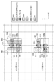
- FIGS. 2 (a) and 2 (b) are plan views of memory cells
- FIGS. 3 (a) to 3 (c) are shown. Is a cross-sectional view of the memory cell in the vertical direction in a plan view.
- FIG. 2A shows an upper portion, that is, a portion including a three-dimensional structure transistor (here, an N-type nanowire FET) formed on a side far from the substrate
- FIG. 2B shows a lower portion, that is, a substrate.
- a portion including a three-dimensional structure transistor (here, an N-type nanowire FET) formed on the near side is shown.
- FIG. 3A is a cross section of line Y1-Y1'
- FIG. 3B is a cross section of line Y2-Y2'
- FIG. 3C is a cross section of line Y3-Y3'.
- the horizontal direction of the drawing is the X direction (corresponding to the first direction)
- the vertical direction of the drawing is the Y direction (corresponding to the second direction)
- the direction perpendicular to the substrate surface It is in the Z direction (corresponding to the depth direction).
- the X direction is the direction in which the gate wiring and the word line extend
- the Y direction is the direction in which the nanowire and the bit wire extend. That is, in the drawings of each embodiment, the XY directions are opposite to those in FIGS. 35 to 38.
- the grids are evenly spaced in the X direction and evenly spaced in the Y direction.
- the grid spacing may be the same or different in the X direction and the Y direction. Further, the grid spacing may be different for each layer.
- each component does not necessarily have to be placed on the grid. However, from the viewpoint of suppressing manufacturing variations, it is preferable that the parts are arranged on the grid.
- the letter "D" is attached to the contact that determines the stored value of the memory cell.
- FIGS. 2A and 2B correspond to the layout of 2 bits of memory cells arranged in the horizontal direction in the memory cell array 3 of FIG.
- a transistor connected to the bit line BL0 is formed in the lower part shown in FIG. 2B, and a transistor connected to the bit line BL1 is formed in the upper part shown in FIG. 2A. That is, the transistors shown in FIGS. 2A and 2B correspond to, for example, the N-type transistors M01 and M00 in the circuit diagram of FIG. 1, respectively.
- the dashed line indicates the frame of the memory cell.
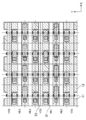
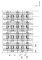
- FIGS. 4 and 5 are diagrams showing the layout structure of the memory cell array using the memory cells of FIGS. 2 and 3, where FIG. 4 shows the upper part and FIG. 5 shows the lower part.
- power supply wirings 11 and 12 extending in the Y direction are provided at both ends of the memory cell in the X direction, respectively.
- Both the power supply wirings 11 and 12 are embedded power supply wirings (BPR: Buried Power Rail) formed in the embedded wiring layer. Both the power supply wirings 11 and 12 supply the power supply voltage VSS.
- wirings 61 and 62 extending in the Y direction are formed in the M1 wiring layer.
- the M1 wiring 61 corresponds to the bit wire BL0
- the M1 wiring 62 corresponds to the bit wire BL1.
- Nanowires 21 extending in the Y direction are formed in the lower part of the memory cell, and nanowires 26 extending in the Y direction are formed in the upper part of the memory cell.
- the nanowires 21 and 26 overlap in a plan view.
- Pads 22a and 22b doped with N-type semiconductors are formed at both ends of the nanowire 21.
- Pads 27a and 27b doped with N-type semiconductors are formed at both ends of the nanowire 26.
- the nanowires 21 form the channel portion of the N-type transistor M00, and the pads 22a and 22b form terminals that serve as the source or drain of the N-type transistor M00.
- the nanowires 26 form the channel portion of the N-type transistor M01, and the pads 27a and 27b form terminals that serve as the source or drain of the N-type transistor M01.
- the N-type transistor M00 is formed above the embedded wiring layer in the Z direction, and the N-type transistor M01 is formed above the N-type transistor M00 in the Z direction.
- the gate wiring 31 extends in the X direction and extends in the Z direction from the lower part to the upper part of the memory cell.
- the gate wiring 31 serves as a gate for the N-type transistors M00 and M01. That is, the nanowire 21, the gate wiring 31, and the pads 22a and 22b constitute the N-type transistor M00.
- the nanowire 26, the gate wiring 31, and the pads 27a and 27b constitute an N-type transistor M01. As will be described later, the gate wiring 31 is connected to the word line WL0.
- a dummy gate wiring 32 is formed at the lower end of the drawing of the memory cell. Like the gate wiring 31, the dummy gate wiring 32 extends in the X direction and the Z direction.
- the nanowires 23 are formed so as to extend from the pad 22b to the lower side of the drawing, and the nanowires 28 are formed so as to extend from the pad 27b to the lower side of the drawing.
- the nanowire 23 and the dummy gate wiring 32, and the nanowire 28 and the dummy gate wiring 32 form N-type transistors DN1 and DN2.
- the dummy gate wiring 32 is connected to VSS (not shown), the N-type transistors DN1 and DN2 are in the off state and do not affect the logical operation of the circuit. It is not described in the circuit diagram of FIG.
- the local wiring 41 and 42 extending in the X direction are formed.
- the local wiring 41 is connected to the pad 22a and extends from the pad 22a to the left in the drawing.
- the local wiring 42 is connected to the pad 22b and extends from the pad 22b to the right in the drawing.
- Local wirings 43 and 44 extending in the X direction are formed in the upper part of the memory cell.
- the local wiring 43 is connected to the pad 27a and extends from the pad 27a to the right in the drawing.
- the local wiring 44 is connected to the pad 27b and extends from the pad 27b to the left in the drawing.
- the local wiring 41 is connected to the M1 wiring 61 via the contact 51.
- the local wiring 43 is connected to the M1 wiring 62 via the contact 52.
- the contacts 71 and 72 determine the stored value of the memory cell depending on the presence or absence of the contacts 71 and 72.
- the contact 71 When the contact 71 is formed, it connects the local wiring 42 and the power supply wiring 12.
- the contact 72 connects the local wiring 44 and the power supply wiring 11 when formed.
- FIG. 4 and 5 show a configuration in which four memory cells of FIG. 2 are arranged in the X direction and four in the Y direction. In the Y direction, the memory cells are arranged so as to be inverted in the Y direction every other row.
- the gate wirings 31 are arranged in a row in the X direction to form word lines WL0 to WL3, respectively. Further, VSS is supplied to the dummy gate wiring 32.
- M1 wirings 61 and 62 are arranged in a row in the Y direction to form bit lines BL0 to BL7, respectively.
- the drains of adjacent transistors are shared between the word lines WL0 and WL1.
- the drains of adjacent transistors are shared between the word lines WL2 and WL3.
- the ROM memory cell includes the transistor M00 provided between the M1 wiring 61 which is a bit wire and the power supply wiring 12 which supplies VSS, and the M1 wiring 62 and VSS which are bit wires.
- the transistor M01 is provided between the power supply wiring 11 and the power supply wiring 11.
- the transistor M01 is formed on the upper layer of the transistor M00, and the channel portion overlaps with the transistor M00 in a plan view.
- the ROM memory cell stores the first data depending on whether or not the local wiring 42 connected to the source of the transistor M00 and the power supply wiring 12 are connected. Further, the ROM memory cell stores the second data depending on whether or not the local wiring 44 connected to the source of the transistor M01 and the power supply wiring 11 are connected.
- the upper transistor and the lower transistor are both N-type transistors, and separate memory cells are formed. Further, the drains of the transistors of the adjacent memory cells in the Y direction are shared with each other. As a result, the area of the semiconductor storage device can be reduced.
- the transistors can be continuously formed in the Y direction. As a result, it is possible to suppress the manufacturing variation of the transistor.
- FIG. 6 is an example of the layout structure of the inverter cell using the CFET.
- the upper transistor N1 shown in FIG. 6A is N-type
- the lower transistor P1 shown in FIG. 6B is P-type.
- the transistor P1 and the transistor N1 are connected in series between the power supply wiring 611 for supplying VDD and the power supply wiring 612 for supplying VSS.
- the transistor P1 has nanowires 621 as a channel portion and pads 622a and 622b.
- the transistor N1 has nanowires 626 as a channel portion and pads 627a and 627b.
- the gate wiring 631 serves as a common gate for the transistor P1 and the transistor N1.
- the M1 wiring 661 which is the input of the inverter, is connected to the gate wiring 631.
- the M1 wiring 662 which is the output of the inverter, is connected to the local wirings 642 and 644 connected to the drains of the transistor P1 and the transistor N1.
- both the lower part and the upper part form N-type transistors. That is, in the semiconductor chip having the mask ROM according to the present embodiment, the lower part of the CFET includes a region which is a P-type transistor and a region which is an N-type transistor.
- the transistor at the lower part may be manufactured as follows, for example. That is, when forming the transistor in the lower part, the portion of the N-type transistor is masked and the other portion is doped into the P conductive type. After that, the portion other than the N-type transistor is masked and the N-conducting type is doped. By arranging the N-type transistor and the P-type transistor apart from each other, it is possible to reliably perform P-conductive doping and N-conductive doping.
- FIGS. 7 to 9 are plan views showing another example of the layout structure of the memory cell according to the present embodiment, in which (a) shows the upper part and (b) shows the lower part, respectively.
- the layout structure of FIGS. 7 to 9 is basically the same as that of FIG. However, it differs from FIG. 2 in the following points.
- the dummy gate wiring 32 is not formed, and the N-type transistors DN1 and DN2 are not formed.
- both the local wirings 41 and 42A extend to the left side of the drawing, and the stored value is set depending on the presence or absence of the contact 71A between the local wiring 42A and the power supply wiring 11.
- both the local wirings 43 and 44A extend to the right side of the drawing, and the stored value is set depending on the presence or absence of the contact 72A between the local wiring 44A and the power supply wiring 12.
- the dummy gate wiring 32 is not formed and the N-type transistors DN1 and DN2 are not formed with respect to the layout structure of FIG.
- the storage value of the memory cell has a layout structure determined by the presence or absence of contact between the local wiring connected to the source of the transistor and the ground power supply wiring.
- the storage value of the memory cell is determined by the presence or absence of contact between the local wiring connected to the drain of the transistor and the bit line.
- FIG. 10 is a plan view of the memory cell according to this modification, (a) is the upper part, and (b) is the lower part.
- the components common to FIG. 2 are designated by the same reference numerals as those of FIG. 2, and detailed description thereof will be omitted here.
- the local wiring 42 is connected to the power supply wiring 12 via the contact 54.
- the local wiring 44 is connected to the power supply wiring 11 via the contact 53.
- the contacts 73 and 74 determine the stored value of the memory cell depending on the presence or absence thereof. When the contact 73 is formed, it connects the local wiring 41 and the M1 wiring 61. When formed, the contact 74 connects the local wiring 43 and the M1 wiring 62.
- a dummy gate wiring 33 is formed at the upper end of the drawing of the memory cell. Like the gate wiring 31, the dummy gate wiring 33 extends in the X direction and the Z direction. However, since the dummy gate wiring 33 is connected to VSS (not shown) like the dummy gate wiring 32 in FIG. 2, it does not affect the logical operation of the circuit.
- 11 and 12 show a configuration in which four memory cells of FIG. 10 are arranged in the X direction and four in the Y direction. In the Y direction, the memory cells are arranged so as to be inverted in the Y direction every other row.
- the gate wirings 31 are arranged in a row in the X direction to form word lines WL0 to WL3, respectively.
- VSS is supplied to the dummy gate wiring 33.
- M1 wirings 61 and 62 are arranged in a row in the Y direction to form bit lines BL0 to BL7, respectively.
- the sources of adjacent transistors are shared between the word lines WL0 and WL1.
- the sources of adjacent transistors are shared between the word lines WL2 and WL3.
- FIGS. 13 to 15 are plan views showing another example of the layout structure of the memory cell according to the present modification, in which (a) shows the upper part and (b) shows the lower part, respectively.
- the layout structure of FIGS. 13 to 15 is basically the same as that of FIG. However, it differs from FIG. 10 in the following points.
- the dummy gate wiring 33 is not formed.
- the direction in which the local wiring extends from the transistor is the same for the source and the drain.
- both the local wirings 41 and 42A extend to the left side of the drawing, and the local wiring 42A and the power supply wiring 11 are connected via the contact 54A.
- the local wirings 43 and 44A both extend to the right side of the drawing, and the local wiring 44A and the power supply wiring 12 are connected via the contact 53A.
- the dummy gate wiring 33 is not formed with respect to the layout structure of FIG.
- FIGS. 16 and 17 are views showing an example of the layout structure of the mask ROM according to the second embodiment
- FIGS. 16 (a) and 16 (b) are plan views of memory cells
- FIGS. 17 (a) to 17 (c) are shown. Is a cross-sectional view of the memory cell in the vertical direction in a plan view. Specifically, FIG. 16A shows the upper part, and FIG. 16B shows the lower part. 17 (a) is a cross section of line Y1-Y1'
- FIG. 17 (b) is a cross section of line Y2-Y2'
- FIG. 17 (c) is a cross section of line Y3-Y3'.
- FIGS. 16A and 16B correspond to the layout of one bit of the memory cell in the memory cell array 3 of FIG.
- a memory cell for one bit is composed of an N-type transistor formed in the upper part shown in FIG. 16A and an N-type transistor formed in the lower part shown in FIG. 16B. That is, the transistors shown in FIGS. 16A and 16B correspond to, for example, the N-type transistor M00 in the circuit diagram of FIG.
- the dashed line indicates the frame of the memory cell.
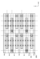
- FIGS. 18 and 19 are diagrams showing the layout structure of the memory cell array using the memory cells of FIGS. 16 and 17, FIG. 18 shows the upper part, and FIG. 19 shows the lower part.
- wirings 161 and 162 extending in the Y direction are formed in the M1 wiring layer.
- the wiring 161 supplies the power supply voltage VSS, and the wiring 162 corresponds to the bit line BL0.
- Nanowires 121 extending in the Y direction are formed in the lower part of the memory cell, and nanowires 126 extending in the Y direction are formed in the upper part of the memory cell.
- the nanowires 121 and 126 overlap in a plan view.
- Pads 122a and 122b doped with N-type semiconductors are formed at both ends of the nanowire 121.
- Pads 127a and 127b doped with N-type semiconductors are formed at both ends of the nanowire 126.
- the nanowires 121 form the channel portion of the N-type transistor Ma, and the pads 122a and 122b form terminals that serve as the source or drain of the N-type transistor Ma.
- the nanowires 126 form the channel portion of the N-type transistor Mb, and the pads 127a and 127b form terminals that serve as the source or drain of the N-type transistor Mb.
- the N-type transistor Ma is formed above the embedded wiring layer in the Z direction, and the N-type transistor Mb is formed above the N-type transistor Ma in the Z direction.
- the gate wiring 131 extends in the X direction and extends in the Z direction from the lower part to the upper part of the memory cell.
- the gate wiring 131 serves as a gate for the N-type transistors Ma and Mb. That is, the nanowire 121, the gate wiring 131, and the pads 122a and 122b constitute the N-type transistor Ma.
- the nanowire 126, the gate wiring 131, and the pads 127a and 127b constitute an N-type transistor Mb.
- the gate wiring 131 is connected to the word line WL0.
- a dummy gate wiring 132 is formed at the lower end of the drawing of the memory cell. Like the gate wiring 131, the dummy gate wiring 132 extends in the X direction and the Z direction.
- the nanowire 123 is formed so as to extend from the pad 122b to the lower side of the drawing, and the nanowire 128 is formed so as to extend from the pad 127b to the lower side of the drawing.
- N-type transistors DN1 and DN2 are formed by the nanowires 123 and the dummy gate wiring 132, and the nanowires 128 and the dummy gate wiring 132. However, since the dummy gate wiring 132 is connected to VSS (not shown), the N-type transistors DN1 and DN2 are in the off state and do not affect the logical operation of the circuit. It is not described in the circuit diagram of FIG.
- local wiring 141 and 142 extending in the X direction are formed.
- the local wiring 141 is connected to the pad 122a and extends from the pad 122a to the right side of the drawing.
- the local wiring 142 is connected to the pad 122b and extends from the pad 122b to the left side of the drawing.
- local wirings 143 and 144 extending in the X direction are formed.
- the local wiring 143 is connected to the pad 127a and extends from the pad 127a to the right side of the drawing.
- the local wiring 144 is connected to the pad 127b and extends from the pad 127b to the left side of the drawing.
- the local wiring 141 is connected to the local wiring 143 via the contact 151.
- the local wiring 142 is connected to the local wiring 144 via the contact 152.
- the local wiring 143 is connected to the M1 wiring 162 via the contact 153.
- the contact 171 determines the stored value of the memory cell depending on the presence or absence of the contact 171.
- the contact 171 connects the local wiring 144 and the M1 wiring 161 when formed.
- FIG. 18 and 19 show a configuration in which four memory cells of FIG. 16 are arranged in the X direction and four in the Y direction. In the Y direction, the memory cells are arranged so as to be inverted in the Y direction every other row.
- the gate wirings 131 are arranged in a row in the X direction to form word lines WL0 to WL3, respectively.
- VSS is supplied to the dummy gate wiring 132.
- M1 wirings 161, 162 are arranged in a row in the Y direction to form wirings for supplying the power supply voltage VSS and bit lines BL0 to BL3, respectively.
- the drains of adjacent transistors are shared between the word lines WL0 and WL1.
- the drains of adjacent transistors are shared between the word lines WL2 and WL3.
- the ROM memory cell includes transistors Ma and Mb provided between the M1 wiring 162 which is a bit line and the M1 wiring 161 which supplies VSS.
- the transistor Mb is formed on the upper layer of the transistor Ma, and the channel portion overlaps with the transistor Ma in a plan view.
- the local wiring 142 connected to the source of the transistor Ma and the local wiring 144 connected to the source of the transistor Mb are connected to each other.
- the local wiring 141 connected to the drain of the transistor Ma and the local wiring 143 connected to the drain of the transistor Mb are connected to each other.
- the ROM memory cell stores data depending on whether or not the local wiring 144 and the M1 wiring 162 are connected. As a result, it is possible to realize a layout structure having a small area for the mask ROM.
- the memory cell for one bit is composed of two transistors formed in the upper part and the lower part, the drive capacity is larger than that in the first embodiment and the operation is performed at high speed. Further, when the characteristics of the transistor vary between the upper part and the lower part, the characteristics vary for each bit line in the first embodiment, but the variation does not affect the present embodiment. Further, since the storage value of the memory cell is set by the contact of the higher layer as compared with the first embodiment, the manufacturing period for changing the storage value of the memory cell can be shortened. On the other hand, in the first embodiment, the area of the memory cell array can be reduced as compared with the present embodiment.
- the wiring for supplying the power supply voltage VSS is arranged between the bit wires, the crosstalk noise between the bit wires can be suppressed. As a result, the operation is stable.
- FIGS. 20 to 22 are plan views showing another example of the layout structure of the memory cell according to the present embodiment, in which (a) shows the upper part and (b) shows the lower part, respectively.
- the layout structure of FIGS. 20 to 22 is basically the same as that of FIG. However, it differs from FIG. 16 in the following points.
- the dummy gate wiring 132 is not formed, and the N-type transistors DN1 and DN2 are not formed.
- a power supply wiring 111 extending in the Y direction is provided at the left end of the drawing of the memory cell.
- the power supply wiring 111 is a BPR formed in the embedded wiring layer and supplies the power supply voltage VSS.
- the contact 172 determines the stored value of the memory cell depending on the presence or absence of the contact 172.
- the contact 172 when formed, connects the local wiring 142 and the power supply wiring 111.
- the M1 wiring 161 is not connected to the memory cell and functions for reducing crosstalk noise between bit lines.
- the gate wiring 132 is not formed and the N-type transistors DN1 and DN2 are not formed with respect to the layout structure of FIG.
- the storage value of the memory cell has a layout structure determined by the presence or absence of contact between the local wiring connected to the source of the transistor and the ground power supply wiring.
- the storage value of the memory cell is determined by the presence or absence of contact between the local wiring connected to the drain of the transistor and the bit line.
- the contact 153 in FIGS. 16 and 17 may be a contact that determines the storage value of the memory cell depending on the presence or absence of the contact 153. Then, the contact 171 is replaced with a contact that connects the local wiring 144 and the wiring 161.
- the memory cell array it may be arranged so that the sources (local wirings 142 and 144) of the transistors adjacent to each other in the Y direction are shared.
- FIG. 23 is a diagram showing an example of the layout structure of the mask ROM according to the third embodiment, and shows a plan view of the memory cell.
- FIG. 23 (a) shows the upper part
- FIG. 23 (b) shows the lower part.
- FIG. 23 corresponds to the layout of two bits of memory cells arranged in the horizontal direction in the memory cell array 3 of FIG.
- a transistor connected to the bit line BL0 is formed in the lower portion shown in FIG. 23 (b), and a transistor connected to the bit line BL1 is formed in the upper portion shown in FIG. 23 (a). That is, the transistors shown in FIGS. 23 (a) and 23 (b) correspond to, for example, the N-type transistors M01 and M00 in the circuit diagram of FIG. 1, respectively.
- the N-type transistors M01 and M00 are both composed of two transistors arranged in the X direction and connected in parallel.
- the dashed line indicates the frame of the memory cell.
- FIG. 24 and 25 are diagrams showing the layout structure of the memory cell array using the memory cell of FIG. 23, FIG. 24 shows the upper part, and FIG. 25 shows the lower part.
- wirings 261,262,263,264 extending in the Y direction are formed in the M1 wiring layer.
- the M1 wiring 261 corresponds to the bit wire BL0
- the wirings 262 and 264 supply the power supply voltage VSS
- the M1 wiring 263 corresponds to the bit wire BL1.
- Nanowires 221 and 223 extending in the Y direction are formed in the lower part of the memory cell, and nanowires 226 and 228 extending in the Y direction are formed in the upper part of the memory cell.
- the nanowires 221,226 overlap in a plan view.
- the nanowires 223 and 228 overlap in a plan view.
- Pads 222a and 222b doped with N-type semiconductors are formed at both ends of the nanowire 221.
- Pads 224a and 224b doped with N-type semiconductors are formed at both ends of the nanowire 223.
- Pads 227a and 227b doped with N-type semiconductors are formed at both ends of the nanowire 226.
- Pads 229a and 229b doped with N-type semiconductors are formed at both ends of the nanowire 228.
- Nanowires 221,223 form the channel portion of the N-type transistor M00, and the pads 222a, 222b, 224a, 224b form terminals that serve as the source or drain of the N-type transistor M00.
- the nanowires 226 and 228 form the channel portion of the N-type transistor M01, and the pads 227a, 227b, 229a, and 229b form terminals that serve as the source or drain of the N-type transistor M01.
- the N-type transistor M00 is formed above the embedded wiring layer in the Z direction, and the N-type transistor M01 is formed above the N-type transistor M00 in the Z direction.
- the gate wiring 231 extends in the X direction and extends in the Z direction from the lower part to the upper part of the memory cell.
- the gate wiring 231 serves as a gate for the N-type transistors M00 and M01. That is, the nanowires 221,223, the gate wiring 231 and the pads 222a, 222b, 224a, 224b constitute the N-type transistor M00.
- the nanowires 226, 228, the gate wiring 231 and the pads 227a, 227b, 229a, 229b constitute the N-type transistor M01. As will be described later, the gate wiring 231 is connected to the word line WL0.
- a dummy gate wiring 232 is formed at the lower end of the drawing of the memory cell.
- the dummy gate wiring 232 extends in the Y direction and the Z direction, similarly to the gate wiring 231.
- Nanowires 225a are formed so as to extend from the pad 222b to the lower side of the drawing, and nanowires 225b are formed so as to extend from the pad 224b to the lower side of the drawing.
- Nanowires 225c are formed so as to extend from the pad 227b to the lower side of the drawing, and nanowires 225d are formed so as to extend from the pad 229b to the lower side of the drawing.
- the N-type transistors DN1 and DN2 are formed by the nanowires 225a and 225b and the dummy gate wiring 232, and the nanowires 225c and 225d and the dummy gate wiring 232. However, since the dummy gate wiring 232 is connected to VSS (not shown), the N-type transistors DN1 and DN2 are in the off state and do not affect the logical operation of the circuit.
- local wirings 241,242 extending in the X direction are formed.
- the local wiring 241 is connected to the pads 222a and 224a and extends from the pad 222a to the left side of the drawing.
- the local wiring 242 is connected to the pads 222b and 224b, and extends from the pads 224b to the right side of the drawing.
- Local wiring 243 and 244 extending in the X direction are formed in the upper part of the memory cell.
- the local wiring 243 is connected to the pads 227a and 229a and extends from the pad 229a to the right side of the drawing.
- the local wiring 244 is connected to the pads 227b and 229b and extends from the pad 227b to the left side of the drawing.
- the local wiring 241 is connected to the M1 wiring 261 via the contact 251.
- the local wiring 243 is connected to the M1 wiring 263 via the contact 252.
- the contacts 271,272 determine the stored value of the memory cell depending on the presence or absence thereof.
- the contact 271 connects the local wiring 242 and the M1 wiring 264 when formed.
- the contact 272, when formed, connects the local wiring 244 and the M1 wiring 262.
- FIG. 24 and 25 show a configuration in which two memory cells of FIG. 23 are arranged in the X direction and four in the Y direction. In the Y direction, the memory cells are arranged so as to be inverted in the Y direction every other row.
- the gate wirings 231 are arranged in a row in the X direction to form word lines WL0 to WL3, respectively.
- VSS is supplied to the dummy gate wiring 232.
- the M1 wirings 261 to 264 are arranged in a row in the Y direction to form the wiring for supplying the power supply voltage VSS and the bit wires BL0 to BL3, respectively.
- the drains of adjacent transistors are shared between the word lines WL0 and WL1.
- the drains of adjacent transistors are shared between the word lines WL2 and WL3.
- the ROM memory cell includes the transistor M00 provided between the M1 wiring 261 which is a bit wire and the M1 wiring 264 which supplies VSS, and the M1 wiring 263 and VSS which are bit wires.
- a transistor M01 provided between the M1 wiring 262 and the M1 wiring 262 is provided.
- the transistor M01 is formed on the upper layer of the transistor M00, and the channel portion overlaps with the transistor M00 in a plan view.
- the transistors M00 and M01 each include two transistors that are arranged in the X direction and share the source and drain.
- the ROM memory cell stores the first data depending on whether or not the local wiring 242 connected to the source shared by the two transistors included in the transistor M00 is connected to the M1 wiring 264. Further, in the ROM memory cell, the second data is stored depending on whether or not the local wiring 244 connected to the source shared by the two transistors included in the transistor M01 is connected to the M1 wiring 262. As a result, it is possible to realize a layout structure having a small area for the mask ROM.
- the transistors constituting the memory cell are assumed to include two transistors connected in parallel, but may include three or more transistors connected in parallel.
- FIGS. 26 to 28 are plan views showing another example of the layout structure of the memory cell according to the present embodiment, in which (a) shows the upper part and (b) shows the lower part, respectively.
- the layout structure of FIGS. 26 to 28 is basically the same as that of FIG. 23. However, it differs from FIG. 23 in the following points.
- the dummy gate wiring 232 is not formed, and the N-type transistors DN1 and DN2 are not formed.
- power supply wirings 211 and 212 extending in the Y direction are provided at both ends of the memory cell drawing.
- the power supply wirings 211 and 212 are BPRs formed in the embedded wiring layer and supply the power supply voltage VSS.
- the contacts 273 and 274 determine the stored value of the memory cell depending on the presence or absence thereof.
- the contact 273, when formed, connects the local wiring 242 and the power supply wiring 212.
- the wirings 262 and 264 are not connected to the memory cell and function for reducing crosstalk noise between the bit lines.
- the gate wiring 232 is not formed and the N-type transistors DN1 and DN2 are not formed with respect to the layout structure of FIG. 27.
- FIGS. 29 and 30 are views showing an example of the layout structure of the mask ROM according to the fourth embodiment
- FIGS. 29 (a) and 30 (b) are plan views of memory cells
- FIGS. 30 (a) to 30 (c) are shown. Is a cross-sectional view of the memory cell in the vertical direction in a plan view. Specifically, FIG. 29 (a) shows the upper part, and FIG. 29 (b) shows the lower part.
- 30 (a) is a cross section of line Y1-Y1'
- FIG. 30 (b) is a cross section of line Y2-Y2'
- FIG. 30 (c) is a cross section of line Y3-Y3'.
- FIGS. 29 (a) and 29 (b) correspond to the layout of two bits of memory cells arranged in the horizontal direction in the memory cell array 3 of FIG.
- a transistor connected to the bit wire BL0 is formed in the lower portion shown in FIG. 29 (b)
- a transistor connected to the bit wire BL1 is formed in the upper portion shown in FIG. 29 (a). That is, the transistors shown in FIGS. 29 (a) and 29 (b) correspond to, for example, the N-type transistors M01 and M00 in the circuit diagram of FIG. 1, respectively.
- the N-type transistors M01 and M00 are each composed of two transistors arranged in the Y direction and connected in parallel.
- the dashed line indicates the frame of the memory cell.
- FIG. 31 and 32 are diagrams showing the layout structure of the memory cell array using the memory cell of FIG. 29, FIG. 31 shows the upper part, and FIG. 32 shows the lower part.
- power supply wirings 411 and 412 extending in the Y direction are provided at both ends of the memory cell in the X direction.
- the power supply wirings 411 and 412 are BPRs, and both supply the power supply voltage VSS.
- wirings 461 and 462 extending in the Y direction are formed in the M1 wiring layer.
- the M1 wiring 461 corresponds to the bit wire BL0
- the M1 wiring 462 corresponds to the bit wire BL1.
- Nanowires 421 and 423 extending in the Y direction are formed in the lower part of the memory cell, and nanowires 426 and 428 extending in the Y direction are formed in the upper part of the memory cell.
- the nanowires 421 and 426 overlap in a plan view, and the nanowires 423 and 428 overlap in a plan view.
- Pads 422a, 422b, 422c doped with N-type semiconductors are formed on the upper side of the drawing of the nanowire 421, between the nanowires 421 and 423, and on the lower side of the drawing of the nanowire 423.
- Pads 427a, 427b, 427c doped with N-type semiconductors are formed on the upper side of the drawing of the nanowire 426, between the nanowires 426 and 428, and on the lower side of the drawing of the nanowire 428.
- Nanowires 421 and 423 form the channel portion of the N-type transistor M00, and the pads 422a, 422b, and 422c form terminals that serve as the source or drain of the N-type transistor M00.
- the pad 422b corresponds to a shared source of the two transistors constituting the N-type transistor M00.
- the nanowires 426 and 428 form the channel portion of the N-type transistor M01, and the pads 427a, 427b and 427c form terminals that serve as the source or drain of the N-type transistor M01.
- the pad 427b corresponds to the shared source of the two transistors constituting the N-type transistor M01.
- the N-type transistor M00 is formed above the embedded wiring layer in the Z direction, and the N-type transistor M01 is formed above the N-type transistor M00 in the Z direction.
- the gate wirings 431 and 432 extend in parallel in the X direction and extend in the Z direction from the lower part to the upper part of the memory cell.
- the gate wirings 431 and 432 serve as gates for the N-type transistors M00 and M01. That is, the nanowires 421 and 423, the gate wirings 431 and 432, and the pads 422a, 422b and 422c constitute the N-type transistor M00.
- the N-type transistor M01 is composed of nanowires 426,428, gate wirings 431,432, and pads 427a, 427b, 427c. As will be described later, the gate wirings 431 and 432 are connected to the same word line WL0.
- local wiring 441, 442, 443 extending in the X direction is formed.
- the local wiring 441 is connected to the pad 422a and extends from the pad 422a to the left in the drawing.
- the local wiring 442 is connected to the pad 422b and extends from the pad 422b to the right in the drawing.
- the local wiring 443 is connected to the pad 422c and extends from the pad 422c to the left in the drawing.
- Local wiring 444,445,446 extending in the X direction is formed in the upper part of the memory cell.
- the local wiring 444 is connected to the pad 427a and extends from the pad 427a to the right in the drawing.
- the local wiring 445 is connected to the pad 427b and extends from the pad 427b to the left in the drawing.
- the local wiring 446 is connected to the pad 427c and extends from the pad 427c to the right in the drawing.
- the local wiring 441 is connected to the M1 wiring 461 via the contact 451.
- the local wiring 443 is connected to the M1 wiring 461 via the contact 452.
- the local wiring 444 is connected to the M1 wiring 462 via the contact 453.
- the local wiring 446 is connected to the M1 wiring 462 via the contact 454.
- the contacts 471 and 472 determine the stored value of the memory cell depending on the presence or absence thereof.
- the contact 471, when formed, connects the local wiring 445 and the power supply wiring 411.
- the contact 472, when formed, connects the local wiring 442 and the power supply wiring 412.
- FIG. 31 and 32 show a configuration in which four memory cells of FIG. 29 are arranged in the X direction and two in the Y direction.
- gate wirings 431 and 432 are arranged in a row in the X direction to form word lines WL0 and WL1, respectively.
- Wiring 461 and 462 in the memory cell of FIG. 29 are arranged in a row in the Y direction to form bit lines BL0 to BL7, respectively.
- the drains of adjacent transistors are shared between the word lines WL0 and WL1.
- the ROM memory cell includes the transistor M00 provided between the M1 wiring 461 which is a bit wire and the power supply wiring 412 which supplies VSS, and the M1 wiring 462 and VSS which are bit wires. It is provided with a transistor M01 provided between the power supply wiring 411 and the power supply wiring 411.
- the transistor M01 is formed on the upper layer of the transistor M00, and the channel portion overlaps with the transistor M00 in a plan view.
- the transistors M00 and M01 each include two transistors that are arranged in the Y direction and share a source with each other.
- the ROM memory cell stores the first data depending on whether or not the local wiring 442 connected to the source as the first node shared by the two transistors included in the transistor M00 is connected to the power supply wiring 412. Further, in the ROM memory cell, the second data is stored depending on whether or not the local wiring 445 connected to the source shared by the two transistors included in the transistor M01 is connected to the power supply wiring 411. As a result, it is possible to realize a layout structure having a small area for the mask ROM.
- (Other layout structure examples) 33 is a plan view showing another example of the layout structure of the memory cell according to the present embodiment, in which (a) shows the upper part and (b) shows the lower part, respectively.
- the layout structure of FIG. 33 is basically the same as that of FIG. 29. However, it differs from FIG. 29 in the following points.
- the direction in which the local wiring extends from the transistor is the same for the source and drain.
- the local wirings 441, 442A and 443 extend to the left side of the drawing, and the stored value is set depending on the presence or absence of the contact 471A between the local wiring 442A and the power supply wiring 411.
- the local wirings 444, 445A and 446 all extend to the right side of the drawing, and the stored value is set depending on the presence or absence of the contact 472A between the local wiring 445A and the power supply wiring 412.
- the storage value of the memory cell has a layout structure determined by the presence or absence of contact between the local wiring connected to the source of the transistor and the ground power supply wiring.
- the storage value of the memory cell is determined by the presence or absence of contact between the local wiring connected to the drain of the transistor and the bit line.
- FIG. 34 is a plan view of the memory cell according to this modification, (a) is the upper part, and (b) is the lower part.
- the components common to FIG. 29 are designated by the same reference numerals as those of FIG. 29, and detailed description thereof will be omitted here.
- local wirings 441A, 442A, 443A extending in the X direction are formed.
- the local wiring 441A is connected to the pad 422a and extends from the pad 422a to the right in the drawing.
- the local wiring 442A is connected to the pad 422b and extends from the pad 422b to the left in the drawing.
- the local wiring 443A is connected to the pad 422c and extends from the pad 422c to the right in the drawing.
- Local wirings 444A, 445A, and 446A extending in the X direction are formed in the upper part of the memory cell.
- the local wiring 444A is connected to the pad 427a and extends from the pad 427a to the left in the drawing.
- the local wiring 445A is connected to the pad 427b and extends from the pad 427b to the right in the drawing.
- the local wiring 446A is connected to the pad 427c and extends from the pad 427c to the left in the drawing.
- the local wiring 441A is connected to the power supply wiring 412 via the contact 457.
- the local wiring 443A is connected to the power supply wiring 412 via the contact 458.
- the local wiring 444A is connected to the power supply wiring 411 via the contact 455.
- the local wiring 446A is connected to the power supply wiring 411 via the contact 456.
- the contacts 473 and 474 determine the stored value of the memory cell depending on the presence or absence of the contacts.
- the contact 473 when formed, connects the local wiring 442A and the M1 wiring 461.
- the contact 474 when formed, connects the local wiring 445A and the M1 wiring 462.
- the transistor is provided with one nanowire, but a part or all of the transistor may be provided with a plurality of nanowires.
- a plurality of nanowires may be provided in the X direction in a plan view, or a plurality of nanowires may be provided in the Z direction.
- a plurality of nanowires may be provided in both the X direction and the Z direction.
- the number of nanowires included in the transistor may be different between the upper part and the lower part of the cell.
- the cross-sectional shape of the nanowire is substantially square, but the present invention is not limited to this. For example, it may be circular or rectangular.
- a nanowire FET has been described as an example as a three-dimensional structure transistor, but the description is not limited to this.
- the transistor formed in the lower part of the cell may be a fin type transistor.
- a semiconductor integrated circuit device provided with a ROM memory cell using a CFET can be provided, which is useful for improving the performance of a semiconductor chip, for example.
Landscapes
- Engineering & Computer Science (AREA)
- Microelectronics & Electronic Packaging (AREA)
- Computer Hardware Design (AREA)
- Semiconductor Memories (AREA)
- Thin Film Transistor (AREA)
Priority Applications (4)
| Application Number | Priority Date | Filing Date | Title |
|---|---|---|---|
| JP2021519379A JP7560746B2 (ja) | 2019-05-13 | 2020-05-01 | 半導体記憶装置 |
| US17/524,535 US11881273B2 (en) | 2019-05-13 | 2021-11-11 | Semiconductor storage device |
| US18/538,722 US12277980B2 (en) | 2019-05-13 | 2023-12-13 | Semiconductor storage device |
| US19/082,854 US20250239316A1 (en) | 2019-05-13 | 2025-03-18 | Semiconductor storage device |
Applications Claiming Priority (2)
| Application Number | Priority Date | Filing Date | Title |
|---|---|---|---|
| JP2019090697 | 2019-05-13 | ||
| JP2019-090697 | 2019-05-13 |
Related Child Applications (1)
| Application Number | Title | Priority Date | Filing Date |
|---|---|---|---|
| US17/524,535 Continuation US11881273B2 (en) | 2019-05-13 | 2021-11-11 | Semiconductor storage device |
Publications (1)
| Publication Number | Publication Date |
|---|---|
| WO2020230665A1 true WO2020230665A1 (ja) | 2020-11-19 |
Family
ID=73290170
Family Applications (1)
| Application Number | Title | Priority Date | Filing Date |
|---|---|---|---|
| PCT/JP2020/018392 Ceased WO2020230665A1 (ja) | 2019-05-13 | 2020-05-01 | 半導体記憶装置 |
Country Status (3)
| Country | Link |
|---|---|
| US (3) | US11881273B2 (https=) |
| JP (1) | JP7560746B2 (https=) |
| WO (1) | WO2020230665A1 (https=) |
Cited By (3)
| Publication number | Priority date | Publication date | Assignee | Title |
|---|---|---|---|---|
| WO2023157724A1 (ja) * | 2022-02-16 | 2023-08-24 | 株式会社ソシオネクスト | 半導体記憶装置 |
| WO2024018875A1 (ja) * | 2022-07-21 | 2024-01-25 | 株式会社ソシオネクスト | 半導体記憶装置 |
| WO2026004616A1 (ja) * | 2024-06-27 | 2026-01-02 | 株式会社ソシオネクスト | 半導体記憶装置 |
Families Citing this family (1)
| Publication number | Priority date | Publication date | Assignee | Title |
|---|---|---|---|---|
| WO2020230665A1 (ja) * | 2019-05-13 | 2020-11-19 | 株式会社ソシオネクスト | 半導体記憶装置 |
Citations (4)
| Publication number | Priority date | Publication date | Assignee | Title |
|---|---|---|---|---|
| US7715246B1 (en) * | 2008-06-27 | 2010-05-11 | Juhan Kim | Mask ROM with light bit line architecture |
| JP2011258898A (ja) * | 2010-06-11 | 2011-12-22 | Toshiba Corp | 半導体装置およびその製造方法 |
| US20160329313A1 (en) * | 2014-06-23 | 2016-11-10 | Synopsys, Inc. | Cells having transistors and interconnects including nanowires or 2d material strips |
| US20180151576A1 (en) * | 2016-11-28 | 2018-05-31 | Samsung Electronics Co., Ltd. | Semiconductor devices |
Family Cites Families (5)
| Publication number | Priority date | Publication date | Assignee | Title |
|---|---|---|---|---|
| DE10335813B4 (de) * | 2003-08-05 | 2009-02-12 | Infineon Technologies Ag | IC-Chip mit Nanowires |
| US8654592B2 (en) * | 2007-06-12 | 2014-02-18 | Micron Technology, Inc. | Memory devices with isolation structures |
| JP4907563B2 (ja) * | 2008-01-16 | 2012-03-28 | パナソニック株式会社 | 半導体記憶装置 |
| TWI739879B (zh) * | 2016-08-10 | 2021-09-21 | 日商東京威力科創股份有限公司 | 用於半導體裝置的延伸區域 |
| WO2020230665A1 (ja) * | 2019-05-13 | 2020-11-19 | 株式会社ソシオネクスト | 半導体記憶装置 |
-
2020
- 2020-05-01 WO PCT/JP2020/018392 patent/WO2020230665A1/ja not_active Ceased
- 2020-05-01 JP JP2021519379A patent/JP7560746B2/ja active Active
-
2021
- 2021-11-11 US US17/524,535 patent/US11881273B2/en active Active
-
2023
- 2023-12-13 US US18/538,722 patent/US12277980B2/en active Active
-
2025
- 2025-03-18 US US19/082,854 patent/US20250239316A1/en active Pending
Patent Citations (4)
| Publication number | Priority date | Publication date | Assignee | Title |
|---|---|---|---|---|
| US7715246B1 (en) * | 2008-06-27 | 2010-05-11 | Juhan Kim | Mask ROM with light bit line architecture |
| JP2011258898A (ja) * | 2010-06-11 | 2011-12-22 | Toshiba Corp | 半導体装置およびその製造方法 |
| US20160329313A1 (en) * | 2014-06-23 | 2016-11-10 | Synopsys, Inc. | Cells having transistors and interconnects including nanowires or 2d material strips |
| US20180151576A1 (en) * | 2016-11-28 | 2018-05-31 | Samsung Electronics Co., Ltd. | Semiconductor devices |
Cited By (3)
| Publication number | Priority date | Publication date | Assignee | Title |
|---|---|---|---|---|
| WO2023157724A1 (ja) * | 2022-02-16 | 2023-08-24 | 株式会社ソシオネクスト | 半導体記憶装置 |
| WO2024018875A1 (ja) * | 2022-07-21 | 2024-01-25 | 株式会社ソシオネクスト | 半導体記憶装置 |
| WO2026004616A1 (ja) * | 2024-06-27 | 2026-01-02 | 株式会社ソシオネクスト | 半導体記憶装置 |
Also Published As
| Publication number | Publication date |
|---|---|
| US20250239316A1 (en) | 2025-07-24 |
| JP7560746B2 (ja) | 2024-10-03 |
| US20220130478A1 (en) | 2022-04-28 |
| US12277980B2 (en) | 2025-04-15 |
| JPWO2020230665A1 (https=) | 2020-11-19 |
| US20240112746A1 (en) | 2024-04-04 |
| US11881273B2 (en) | 2024-01-23 |
Similar Documents
| Publication | Publication Date | Title |
|---|---|---|
| US7075820B2 (en) | Semiconductor memory device for dynamically storing data with channel body of transistor used as storage node | |
| US8169030B2 (en) | Semiconductor memory device and production method thereof | |
| US9373386B2 (en) | Dual-port SRAM systems | |
| KR100423896B1 (ko) | 축소가능한 2개의 트랜지스터 기억 소자 | |
| JP7560746B2 (ja) | 半導体記憶装置 | |
| US12225719B2 (en) | Semiconductor storage device | |
| US20220108992A1 (en) | Semiconductor storage device | |
| US12279419B2 (en) | Semiconductor storage device having rom cells including nanosheet field effect transistors | |
| US20020160581A1 (en) | Semiconductor device | |
| US20250151267A1 (en) | Semiconductor memory device | |
| US6590802B2 (en) | Semiconductor storage apparatus | |
| US11688480B2 (en) | Semiconductor storage device | |
| US20240395709A1 (en) | Semiconductor memory device | |
| EP4326024A2 (en) | Fin field-effect transistor (finfet) based semiconductor memory array having memory cells with a reduced surface area | |
| JPH0637269A (ja) | 接合型電界効果トランジスタ、その接合型電界効果トランジスタを含む半導体記憶装置およびそれらの製造方法 | |
| US6445017B2 (en) | Full CMOS SRAM cell | |
| CN120751698A (zh) | 存储器结构、其制造方法、其操作方法及存储器阵列 | |
| US7825471B2 (en) | Semiconductor memory device including SRAM cell having well power potential supply region provided therein | |
| JP2001024070A (ja) | 半導体記憶装置 | |
| JP7762991B1 (ja) | 半導体素子を用いたメモリ装置 | |
| US20260013096A1 (en) | Bit line with non-uniform width in a memory array | |
| KR930001733B1 (ko) | 반도체 기억장치 | |
| US20210091090A1 (en) | Memory array with continuous diffusion for bit-cells and support circuitry | |
| TW202412267A (zh) | 動態隨機存取記憶體結構 |
Legal Events
| Date | Code | Title | Description |
|---|---|---|---|
| 121 | Ep: the epo has been informed by wipo that ep was designated in this application |
Ref document number: 20804900 Country of ref document: EP Kind code of ref document: A1 |
|
| ENP | Entry into the national phase |
Ref document number: 2021519379 Country of ref document: JP Kind code of ref document: A |
|
| NENP | Non-entry into the national phase |
Ref country code: DE |
|
| 122 | Ep: pct application non-entry in european phase |
Ref document number: 20804900 Country of ref document: EP Kind code of ref document: A1 |