WO2020217138A2 - 半導体装置、及び半導体装置の動作方法 - Google Patents
半導体装置、及び半導体装置の動作方法 Download PDFInfo
- Publication number
- WO2020217138A2 WO2020217138A2 PCT/IB2020/053526 IB2020053526W WO2020217138A2 WO 2020217138 A2 WO2020217138 A2 WO 2020217138A2 IB 2020053526 W IB2020053526 W IB 2020053526W WO 2020217138 A2 WO2020217138 A2 WO 2020217138A2
- Authority
- WO
- WIPO (PCT)
- Prior art keywords
- wiring
- circuit
- transistor
- potential
- insulator
- Prior art date
- Legal status (The legal status is an assumption and is not a legal conclusion. Google has not performed a legal analysis and makes no representation as to the accuracy of the status listed.)
- Ceased
Links
Images


Classifications
-
- G—PHYSICS
- G11—INFORMATION STORAGE
- G11C—STATIC STORES
- G11C11/00—Digital stores characterised by the use of particular electric or magnetic storage elements; Storage elements therefor
- G11C11/56—Digital stores characterised by the use of particular electric or magnetic storage elements; Storage elements therefor using storage elements with more than two stable states represented by steps, e.g. of voltage, current, phase, frequency
- G11C11/565—Digital stores characterised by the use of particular electric or magnetic storage elements; Storage elements therefor using storage elements with more than two stable states represented by steps, e.g. of voltage, current, phase, frequency using capacitive charge storage elements
-
- G—PHYSICS
- G11—INFORMATION STORAGE
- G11C—STATIC STORES
- G11C11/00—Digital stores characterised by the use of particular electric or magnetic storage elements; Storage elements therefor
- G11C11/21—Digital stores characterised by the use of particular electric or magnetic storage elements; Storage elements therefor using electric elements
- G11C11/34—Digital stores characterised by the use of particular electric or magnetic storage elements; Storage elements therefor using electric elements using semiconductor devices
- G11C11/40—Digital stores characterised by the use of particular electric or magnetic storage elements; Storage elements therefor using electric elements using semiconductor devices using transistors
- G11C11/401—Digital stores characterised by the use of particular electric or magnetic storage elements; Storage elements therefor using electric elements using semiconductor devices using transistors forming cells needing refreshing or charge regeneration, i.e. dynamic cells
- G11C11/403—Digital stores characterised by the use of particular electric or magnetic storage elements; Storage elements therefor using electric elements using semiconductor devices using transistors forming cells needing refreshing or charge regeneration, i.e. dynamic cells with charge regeneration common to a multiplicity of memory cells, i.e. external refresh
- G11C11/405—Digital stores characterised by the use of particular electric or magnetic storage elements; Storage elements therefor using electric elements using semiconductor devices using transistors forming cells needing refreshing or charge regeneration, i.e. dynamic cells with charge regeneration common to a multiplicity of memory cells, i.e. external refresh with three charge-transfer gates, e.g. MOS transistors, per cell
-
- G—PHYSICS
- G11—INFORMATION STORAGE
- G11C—STATIC STORES
- G11C11/00—Digital stores characterised by the use of particular electric or magnetic storage elements; Storage elements therefor
- G11C11/21—Digital stores characterised by the use of particular electric or magnetic storage elements; Storage elements therefor using electric elements
- G11C11/34—Digital stores characterised by the use of particular electric or magnetic storage elements; Storage elements therefor using electric elements using semiconductor devices
- G11C11/40—Digital stores characterised by the use of particular electric or magnetic storage elements; Storage elements therefor using electric elements using semiconductor devices using transistors
- G11C11/401—Digital stores characterised by the use of particular electric or magnetic storage elements; Storage elements therefor using electric elements using semiconductor devices using transistors forming cells needing refreshing or charge regeneration, i.e. dynamic cells
- G11C11/4063—Auxiliary circuits, e.g. for addressing, decoding, driving, writing, sensing or timing
- G11C11/407—Auxiliary circuits, e.g. for addressing, decoding, driving, writing, sensing or timing for memory cells of the field-effect type
- G11C11/409—Read-write [R-W] circuits
- G11C11/4091—Sense or sense/refresh amplifiers, or associated sense circuitry, e.g. for coupled bit-line precharging, equalising or isolating
-
- G—PHYSICS
- G11—INFORMATION STORAGE
- G11C—STATIC STORES
- G11C11/00—Digital stores characterised by the use of particular electric or magnetic storage elements; Storage elements therefor
- G11C11/56—Digital stores characterised by the use of particular electric or magnetic storage elements; Storage elements therefor using storage elements with more than two stable states represented by steps, e.g. of voltage, current, phase, frequency
- G11C11/5621—Digital stores characterised by the use of particular electric or magnetic storage elements; Storage elements therefor using storage elements with more than two stable states represented by steps, e.g. of voltage, current, phase, frequency using charge storage in a floating gate
- G11C11/5642—Sensing or reading circuits; Data output circuits
-
- H—ELECTRICITY
- H10—SEMICONDUCTOR DEVICES; ELECTRIC SOLID-STATE DEVICES NOT OTHERWISE PROVIDED FOR
- H10D—INORGANIC ELECTRIC SEMICONDUCTOR DEVICES
- H10D30/00—Field-effect transistors [FET]
- H10D30/60—Insulated-gate field-effect transistors [IGFET]
- H10D30/67—Thin-film transistors [TFT]
- H10D30/674—Thin-film transistors [TFT] characterised by the active materials
- H10D30/6755—Oxide semiconductors, e.g. zinc oxide, copper aluminium oxide or cadmium stannate
-
- H—ELECTRICITY
- H10—SEMICONDUCTOR DEVICES; ELECTRIC SOLID-STATE DEVICES NOT OTHERWISE PROVIDED FOR
- H10D—INORGANIC ELECTRIC SEMICONDUCTOR DEVICES
- H10D30/00—Field-effect transistors [FET]
- H10D30/60—Insulated-gate field-effect transistors [IGFET]
- H10D30/67—Thin-film transistors [TFT]
- H10D30/6757—Thin-film transistors [TFT] characterised by the structure of the channel, e.g. transverse or longitudinal shape or doping profile
-
- H—ELECTRICITY
- H10—SEMICONDUCTOR DEVICES; ELECTRIC SOLID-STATE DEVICES NOT OTHERWISE PROVIDED FOR
- H10D—INORGANIC ELECTRIC SEMICONDUCTOR DEVICES
- H10D30/00—Field-effect transistors [FET]
- H10D30/60—Insulated-gate field-effect transistors [IGFET]
- H10D30/68—Floating-gate IGFETs
-
- H—ELECTRICITY
- H10—SEMICONDUCTOR DEVICES; ELECTRIC SOLID-STATE DEVICES NOT OTHERWISE PROVIDED FOR
- H10D—INORGANIC ELECTRIC SEMICONDUCTOR DEVICES
- H10D30/00—Field-effect transistors [FET]
- H10D30/60—Insulated-gate field-effect transistors [IGFET]
- H10D30/69—IGFETs having charge trapping gate insulators, e.g. MNOS transistors
-
- H—ELECTRICITY
- H10—SEMICONDUCTOR DEVICES; ELECTRIC SOLID-STATE DEVICES NOT OTHERWISE PROVIDED FOR
- H10D—INORGANIC ELECTRIC SEMICONDUCTOR DEVICES
- H10D87/00—Integrated devices comprising both bulk components and either SOI or SOS components on the same substrate
-
- G—PHYSICS
- G11—INFORMATION STORAGE
- G11C—STATIC STORES
- G11C2211/00—Indexing scheme relating to digital stores characterized by the use of particular electric or magnetic storage elements; Storage elements therefor
- G11C2211/56—Indexing scheme relating to G11C11/56 and sub-groups for features not covered by these groups
- G11C2211/563—Multilevel memory reading aspects
- G11C2211/5634—Reference cells
Definitions
- One aspect of the present invention relates to a semiconductor device and a method of operating the semiconductor device.
- one aspect of the present invention is not limited to the above technical fields.
- the technical field of the invention disclosed in the present specification and the like relates to an object, an operation method (driving method), or a manufacturing method.
- one aspect of the invention relates to a process, machine, manufacture, or composition (composition of matter). Therefore, more specifically, the technical fields of one aspect of the present invention disclosed in the present specification include semiconductor devices, display devices, liquid crystal display devices, light emitting devices, power storage devices, image pickup devices, storage devices, signal processing devices, and processors.
- Electronic devices, systems, their driving methods, their manufacturing methods, or their inspection methods can be mentioned as examples.
- the semiconductor device As a means for increasing the storage capacity of the semiconductor device, for example, increasing the holding potential can be mentioned.
- a voltage distribution is required for each data according to the number of bits that can be held in the memory cell. For example, in the case of a memory cell capable of holding 2 bits, four voltage distributions are required, and therefore, three threshold voltages as a reference for identifying the four voltage distributions are required.
- the semiconductor device preferably has a circuit that accurately reads the value of the multi-valued data.
- One aspect of the present invention is to provide a semiconductor device that can hold multi-valued data and can read out multi-valued data.
- one aspect of the present invention is to provide a semiconductor device having an improved bit density.
- one aspect of the present invention is to provide a novel semiconductor device.
- one aspect of the present invention is to provide a novel operating method for a semiconductor device.
- the problem of one aspect of the present invention is not limited to the problems listed above.
- the issues listed above do not preclude the existence of other issues.
- Other issues are issues not mentioned in this item, which are described below. Issues not mentioned in this item can be derived from descriptions in the description, drawings, etc. by those skilled in the art, and can be appropriately extracted from these descriptions.
- one aspect of the present invention solves at least one of the above-listed problems and other problems. It should be noted that one aspect of the present invention does not need to solve all of the problems listed above and other problems.
- One aspect of the present invention includes a memory cell, a first reference cell, a second reference cell, a first sense amplifier, a second sense amplifier, a first circuit, a second circuit, and a third circuit. It has a first switch, a second switch, a first wiring, a second wiring, a third wiring, and a fourth wiring, and the memory cell is electrically connected to the first circuit and is the first.
- the reference cell is electrically connected to the second circuit
- the second reference cell is electrically connected to the third circuit
- the first wiring is the first circuit, the first terminal of the first switch, and the first.
- the first sense amplifier is electrically connected, the second wiring is electrically connected to the second circuit, the first terminal of the second switch, and the first sense amplifier, and the third wiring is the third wiring. It is electrically connected to the second terminal of the 1 switch and the second sense amplifier, and the fourth wiring is electrically connected to the third circuit, the second terminal of the second switch, and the second sense amplifier.
- the first circuit is connected and has a function of outputting the first potential to the first wiring and the third wiring according to the first signal output from the memory cell when the first switch is on.
- the second circuit has a function of outputting a second potential to the second wiring according to the second signal output from the first reference cell when the second switch is off, and the third circuit has a function of outputting the second potential to the second wiring. It is a semiconductor device having a function of outputting a third potential to a fourth wiring according to a third signal output from a second reference cell when the second switch is in the off state.
- one aspect of the present invention is a memory cell, a first reference cell, a second reference cell, a first sense amplifier, a second sense amplifier, a first circuit, a second circuit, and a third circuit.
- a first switch, a second switch, a first wiring, a second wiring, a third wiring, and a fourth wiring, and the memory cell is electrically connected to the first circuit.
- the first reference cell is electrically connected to the second circuit
- the second reference cell is electrically connected to the third circuit
- the first wiring is the first circuit and the first terminal of the first switch.
- the second wiring is electrically connected to the second circuit, the first terminal of the second switch, and the first sense amplifier
- the third wiring is electrically connected to the first sense amplifier.
- the second terminal of the first switch and the second sense amplifier are electrically connected, and the fourth wiring is electrically connected to the third circuit, the second terminal of the second switch, and the second sense amplifier.
- the first circuit has a function of outputting the first potential to the first wiring and the third wiring according to the first signal output from the memory cell when the first switch is on.
- the second circuit has a function of outputting the second potential to the second wiring according to the second signal output from the first reference cell when the second switch is off, and the third circuit. Is a semiconductor device having a function of outputting a third potential to a fourth wiring according to a third signal output from a second reference cell when the second switch is in the off state.
- the first circuit has a first transistor
- the second circuit has a second transistor
- the third circuit has a second transistor.
- the gate of the first transistor is electrically connected to the memory cell
- the first terminal of the first transistor is electrically connected to the first wiring
- the gate of the second transistor is Electrically connected to the first reference cell
- the first terminal of the second transistor is electrically connected to the second wiring
- the gate of the third transistor is electrically connected to the second reference cell
- the third The first terminal of the transistor is a semiconductor device that is electrically connected to the third wiring.
- the memory cell has a fourth transistor and a capacitance, and the first terminal of the fourth transistor has a fourth transistor.
- the second terminal of the fourth transistor which is electrically connected to the first terminal of the capacitance, is a semiconductor device which is electrically connected to the first circuit.
- one aspect of the present invention has a first layer and a second layer in the configuration of the above (4), and the first layer has a first sense amplifier and a second sense amplifier.
- the second layer has a memory cell, a first reference cell, and a second reference cell, the second layer is located above the first layer, and each of the first to fourth transistors is located.
- the transistor contained in each of the first sense amplifier and the second sense amplifier having a metal oxide in the channel forming region is a semiconductor device having silicon in the channel forming region.
- one aspect of the present invention is a memory cell, a first reference cell, a second reference cell, a first sense amplifier, a second sense amplifier, a first circuit, a second circuit, and a third circuit.
- a first switch, a second switch, a first wiring, a second wiring, a third wiring, and a fourth wiring, and the memory cell is electrically connected to the first circuit.
- the first reference cell is electrically connected to the second circuit
- the second reference cell is electrically connected to the third circuit
- the first wiring is the first circuit and the first terminal of the first switch.
- the second wiring is electrically connected to the second circuit, the first terminal of the second switch, and the first sense amplifier
- the third wiring is electrically connected to the first sense amplifier.
- the second terminal of the first switch and the second sense amplifier are electrically connected, and the fourth wiring is electrically connected to the third circuit, the second terminal of the second switch, and the second sense amplifier. It is a method of operating a semiconductor device that is specifically connected to each other and has a first period to a sixth period.
- the first period is a period during which a first signal output from a memory cell is input to a first circuit.
- the second period has a period in which the first switch is in the ON state and the first circuit outputs the first potential to the first wiring and the third wiring in response to the first signal.
- the third period has a period in which the second switch is turned off, and in the fourth period, the second signal output from the first reference cell is input to the second circuit, and the second circuit becomes the second signal.
- the corresponding period for outputting the second potential to the second wiring and the third signal output from the second reference cell are input to the third circuit, and the third circuit responds to the third signal, the third potential.
- the fifth period has a period of turning off the first switch
- the sixth period is the first potential of the first wiring by the first sense amplifier.
- the first potential of the first wiring is changed to either a high level potential or a low level potential
- the second potential of the second wiring is changed to a high level potential or a low level potential.
- the second sense amplifier refers to the first potential of the third wiring and the third potential of the fourth wiring, and sets the first potential of the third wiring to a high level potential or a low level potential. It is an operation method of a semiconductor device having a period of changing to one side and changing the third potential of the fourth wiring to the other side of a high level potential or a low level potential.
- the first circuit has a first transistor
- the second circuit has a second transistor
- the third circuit has a third transistor.
- the gate of the first transistor is electrically connected to the memory cell
- the first terminal of the first transistor is electrically connected to the first wiring
- the gate of the second transistor is the first reference cell.
- the first terminal of the second transistor is electrically connected to the second wiring
- the gate of the third transistor is electrically connected to the second reference cell
- the first terminal of the third transistor is electrically connected to.
- the terminal is a method of operating a semiconductor device that is electrically connected to the third wiring.
- the memory cell has a fourth transistor and a capacitance, and the first terminal of the fourth transistor has a capacitance.
- the second terminal of the fourth transistor which is electrically connected to the first terminal, is a method of operating a semiconductor device, which is electrically connected to the first circuit.
- one aspect of the present invention includes a first layer and a second layer in the operation method (8) above, and the first layer includes a first sense amplifier and a second sense amplifier.
- the second layer has a memory cell, a first reference cell, and a second reference cell, and the second layer is located above the first layer and has, respectively, the first to fourth transistors. Is a method of operating a semiconductor device, which has a metal oxide in the channel forming region, and the transistors included in each of the first sense amplifier and the second sense amplifier have silicon in the channel forming region. ..
- the semiconductor device is a device that utilizes semiconductor characteristics, and refers to a circuit including a semiconductor element (transistor, diode, photodiode, etc.), a device having the same circuit, and the like. It also refers to all devices that can function by utilizing semiconductor characteristics. For example, an integrated circuit, a chip having an integrated circuit, and an electronic component in which the chip is housed in a package are examples of semiconductor devices. Further, the storage device, the display device, the light emitting device, the lighting device, the electronic device, and the like are themselves semiconductor devices, and may have the semiconductor device.
- an element for example, a switch, a transistor, a capacitance element, an inductor, a resistance element, a diode, a display
- One or more devices, light emitting devices, loads, etc. can be connected between X and Y.
- the switch has a function of controlling on / off. That is, the switch is in a conductive state (on state) or a non-conducting state (off state), and has a function of controlling whether or not a current flows.
- a circuit that enables functional connection between X and Y for example, a logic circuit (inverter, NAND circuit, NOR circuit, etc.), signal conversion, etc.) Circuits (DA conversion circuit, AD conversion circuit, gamma correction circuit, etc.), potential level conversion circuit (power supply circuit (boost circuit, step-down circuit, etc.), level shifter circuit that changes the signal potential level, etc.), voltage source, current source, switching Circuits, amplification circuits (circuits that can increase signal amplitude or current amount, operational amplifiers, differential amplification circuits, source follower circuits, buffer circuits, etc.), signal generation circuits, storage circuits, control circuits, etc.) are X and Y. It is possible to connect one or more in between. As an example, even if another circuit is sandwiched between X and Y, if the signal output from X is transmitted to Y, it is assumed that X and Y are functionally connected.
- X and Y are electrically connected, it means that X and Y are electrically connected (that is, another element between X and Y). Or, when they are connected by sandwiching another circuit) and when X and Y are functionally connected (that is, when they are functionally connected by sandwiching another circuit between X and Y). (Is) and the case where X and Y are directly connected (that is, the case where another element or another circuit is not sandwiched between X and Y) is included. In other words, the case of explicitly stating that it is electrically connected is the same as the case of explicitly stating that it is simply connected.
- X and Y, the source (or the first terminal, etc.) and the drain (or the second terminal, etc.) of the transistor are electrically connected to each other, and the X, the source (or the second terminal, etc.) of the transistor are connected to each other. (1 terminal, etc.), the drain of the transistor (or the 2nd terminal, etc.), and Y are electrically connected in this order.
- the source of the transistor (or the first terminal, etc.) is electrically connected to X
- the drain of the transistor (or the second terminal, etc.) is electrically connected to Y
- the X, the source of the transistor (such as the second terminal).
- first terminal, etc.), the drain of the transistor (or the second terminal, etc.), and Y are electrically connected in this order.
- X is electrically connected to Y via the source (or first terminal, etc.) and drain (or second terminal, etc.) of the transistor, and X, the source (or first terminal, etc.) of the transistor.
- the terminals, etc.), the drain of the transistor (or the second terminal, etc.), and Y are provided in this connection order.
- the source (or first terminal, etc.) and drain (or second terminal, etc.) of the transistor can be separated. Separately, the technical scope can be determined. It should be noted that these expression methods are examples and are not limited to these expression methods.
- X and Y are assumed to be objects (for example, devices, elements, circuits, wirings, electrodes, terminals, conductive films, layers, etc.).
- the circuit diagram shows that the independent components are electrically connected to each other, the case where one component has the functions of a plurality of components together.
- one component has the functions of a plurality of components together.
- the electrical connection in the present specification also includes the case where one conductive film has the functions of a plurality of components in combination.
- the “resistance element” can be, for example, a circuit element, wiring, or the like having a resistance value higher than 0 ⁇ . Therefore, in the present specification and the like, the “resistive element” includes a wiring having a resistance value, a transistor in which a current flows between a source and a drain, a diode, a coil, and the like. Therefore, the term “resistance element” can be paraphrased into terms such as “resistance”, “load”, and “region having a resistance value”, and conversely, “resistance", “load”, and “region having a resistance value”. Can be rephrased as a term such as “resistive element”.
- the resistance value can be, for example, preferably 1 m ⁇ or more and 10 ⁇ or less, more preferably 5 m ⁇ or more and 5 ⁇ or less, and further preferably 10 m ⁇ or more and 1 ⁇ or less. Further, for example, it may be 1 ⁇ or more and 1 ⁇ 10 9 ⁇ or less.
- the “capacitance element” means, for example, a circuit element having a capacitance value higher than 0F, a wiring region having a capacitance value, a parasitic capacitance, a transistor gate capacitance, and the like. Can be. Therefore, in the present specification and the like, the “capacitive element” is not only a circuit element containing a pair of electrodes and a dielectric contained between the electrodes, but also a parasitic element appearing between the wirings. It shall include the capacitance, the gate capacitance that appears between the gate and one of the source or drain of the transistor, and the like.
- capacitor element means “capacitive element” and “parasitic capacitance”. It can be paraphrased into terms such as “capacity” and “gate capacitance”.
- the term “pair of electrodes” in “capacity” can be paraphrased as "a pair of conductors", “a pair of conductive regions", “a pair of regions” and the like.
- the value of the capacitance can be, for example, 0.05 fF or more and 10 pF or less. Further, for example, it may be 1 pF or more and 10 ⁇ F or less.
- the transistor has three terminals called a gate, a source, and a drain.
- the gate is a control terminal that controls the conduction state of the transistor.
- the two terminals that function as sources or drains are the input and output terminals of the transistor.
- One of the two input / output terminals becomes a source and the other becomes a drain depending on the high and low potentials given to the conductive type (n-channel type, p-channel type) of the transistor and the three terminals of the transistor. Therefore, in the present specification and the like, the terms source and drain can be paraphrased.
- transistors when explaining the connection relationship of transistors, "one of the source or drain” (or the first electrode or the first terminal), “the other of the source or drain” (or the second electrode, or The notation (second terminal) is used.
- it may have a back gate in addition to the above-mentioned three terminals.
- one of the transistor gate or the back gate may be referred to as a first gate
- the other of the transistor gate or the back gate may be referred to as a second gate.
- the terms “gate” and “backgate” may be interchangeable.
- the respective gates When the transistor has three or more gates, the respective gates may be referred to as a first gate, a second gate, a third gate, and the like in the present specification and the like.
- a node can be paraphrased as a terminal, a wiring, an electrode, a conductive layer, a conductor, an impurity region, etc., depending on a circuit configuration, a device structure, and the like.
- terminals, wiring, etc. can be paraphrased as nodes.
- ground potential ground potential
- the potentials are relative, and when the reference potential changes, the potential given to the wiring, the potential applied to the circuit or the like, the potential output from the circuit or the like also changes.
- the terms “high level potential” and “low level potential” do not mean a specific potential.
- both of the two wires “function as wires that supply high level potentials”
- the high level potentials provided by both wires do not have to be equal to each other.
- both of the two wires are described as “functioning as a wire that supplies a low level potential”
- the low level potentials given by both wires do not have to be equal to each other. ..
- the "current” is a charge transfer phenomenon (electrical conduction).
- the description “electrical conduction of a positively charged body is occurring” means “electrical conduction of a negatively charged body in the opposite direction”. Is happening. " Therefore, in the present specification and the like, “current” refers to a charge transfer phenomenon (electrical conduction) accompanying the movement of carriers, unless otherwise specified.
- the carrier here include electrons, holes, anions, cations, complex ions, and the like, and the carriers differ depending on the system in which the current flows (for example, semiconductor, metal, electrolyte, vacuum, etc.).
- the "current direction” in the wiring or the like is the direction in which the positive carrier moves, and is described as a positive current amount.
- the direction in which the negative carrier moves is opposite to the direction of the current, and is expressed by the amount of negative current. Therefore, in the present specification and the like, if there is no notice about the positive or negative of the current (or the direction of the current), the description such as “current flows from element A to element B” means “current flows from element B to element A”. It can be paraphrased as. Further, the description such as “a current is input to the element A” can be rephrased as "a current is output from the element A” or the like.
- the ordinal numbers “first”, “second”, and “third” are added to avoid confusion of the components. Therefore, the number of components is not limited. Moreover, the order of the components is not limited. For example, the component referred to in “first” in one of the embodiments of the present specification and the like may be a component referred to in “second” in another embodiment or in the claims. There can also be. Further, for example, the component referred to in “first” in one of the embodiments of the present specification and the like may be omitted in another embodiment or in the claims.
- the terms “above” and “below” do not limit the positional relationship of the components directly above or below and in direct contact with each other.
- the electrode B does not have to be formed in direct contact with the insulating layer A, and another configuration is formed between the insulating layer A and the electrode B. Do not exclude those that contain elements.
- membrane and layer can be interchanged with each other depending on the situation.
- the terms “insulating layer” and “insulating film” may be changed to the term "insulator”.
- Electrode may be used as part of a “wiring” and vice versa.
- the terms “electrode” and “wiring” include the case where a plurality of “electrodes” and “wiring” are integrally formed.
- a “terminal” may be used as part of a “wiring” or “electrode” and vice versa.
- the term “terminal” includes a case where a plurality of "electrodes", “wiring”, “terminals” and the like are integrally formed.
- the "electrode” can be a part of the “wiring” or the “terminal”, and for example, the “terminal” can be a part of the “wiring” or the “electrode”.
- terms such as “electrode”, “wiring”, and “terminal” may be replaced with terms such as "area” in some cases.
- terms such as “wiring”, “signal line”, and “power line” can be interchanged with each other in some cases or depending on the situation.
- the reverse is also true, and it may be possible to change terms such as “signal line” and “power line” to the term “wiring”.
- a term such as “power line” may be changed to a term such as "signal line”.
- terms such as “signal line” may be changed to terms such as "power line”.
- the term “potential” applied to the wiring may be changed to a term such as “signal” in some cases or depending on the situation.
- the reverse is also true, and terms such as “signal” may be changed to the term “potential”.
- semiconductor impurities refer to, for example, components other than the main components constituting the semiconductor layer.
- an element having a concentration of less than 0.1 atomic% is an impurity. Due to the inclusion of impurities, for example, DOS (Density of States) may be formed in the semiconductor, carrier mobility may be lowered, crystallinity may be lowered, and the like.
- the impurities that change the characteristics of the semiconductor include, for example, group 1 element, group 2 element, group 13 element, group 14 element, group 15 element, and other than the main component.
- transition metals and the like and in particular, hydrogen (also contained in water), lithium, sodium, silicon, boron, phosphorus, carbon, nitrogen and the like.
- impurities that change the characteristics of the semiconductor include, for example, Group 1 elements other than oxygen and hydrogen, Group 2 elements, Group 13 elements, Group 15 elements, and the like. There is.
- the switch means a switch that is in a conductive state (on state) or a non-conducting state (off state) and has a function of controlling whether or not a current flows.
- the switch has a function of selecting and switching the path through which the current flows.
- an electric switch, a mechanical switch, or the like can be used. That is, the switch is not limited to a specific switch as long as it can control the current.
- Examples of electrical switches include transistors (for example, bipolar transistors, MOS transistors, etc.), diodes (for example, PN diodes, PIN diodes, Schottky diodes, MIM (Metal Insulator Molecular) diodes, and MIS (Metal Insulator Semiconductor) diodes. , Diode-connected transistors, etc.), or logic circuits that combine these.
- transistors for example, bipolar transistors, MOS transistors, etc.
- diodes for example, PN diodes, PIN diodes, Schottky diodes, MIM (Metal Insulator Molecular) diodes, and MIS (Metal Insulator Semiconductor) diodes. , Diode-connected transistors, etc.
- the "conducting state" of the transistor means a state in which the source electrode and the drain electrode of the transistor can be regarded as being electrically short-circuited.
- the "non-conducting state" of the transistor means a state in which the source electrode and the drain electrode of the transistor can be regarded as being electrically cut off.
- the polarity (conductive type) of the transistor is not particularly limited.
- An example of a mechanical switch is a switch that uses MEMS (Micro Electro Mechanical System) technology.
- the switch has an electrode that can be moved mechanically, and by moving the electrode, it operates by controlling conduction and non-conduction.
- parallel means a state in which two straight lines are arranged at an angle of -10 ° or more and 10 ° or less. Therefore, the case of ⁇ 5 ° or more and 5 ° or less is also included.
- substantially parallel or approximately parallel means a state in which two straight lines are arranged at an angle of ⁇ 30 ° or more and 30 ° or less.
- vertical means a state in which two straight lines are arranged at an angle of 80 ° or more and 100 ° or less. Therefore, the case of 85 ° or more and 95 ° or less is also included.
- substantially vertical or “approximately vertical” means a state in which two straight lines are arranged at an angle of 60 ° or more and 120 ° or less.
- one aspect of the present invention it is possible to provide a semiconductor device that can hold multi-valued data and can read out multi-valued data.
- one aspect of the present invention can provide a semiconductor device having an improved bit density.
- a novel semiconductor device can be provided by one aspect of the present invention.
- one aspect of the present invention can provide a novel method of operating a semiconductor device.
- the effect of one aspect of the present invention is not limited to the effects listed above.
- the effects listed above do not preclude the existence of other effects.
- the other effects are the effects not mentioned in this item, which are described below. Effects not mentioned in this item can be derived from those described in the description, drawings, etc. by those skilled in the art, and can be appropriately extracted from these descriptions.
- one aspect of the present invention has at least one of the above-listed effects and other effects. Therefore, one aspect of the present invention may not have the effects listed above in some cases.
- FIG. 1 is a block diagram showing a configuration example of a semiconductor device.
- 2A and 2B are block diagrams showing a configuration example of a circuit included in the semiconductor device.
- 3A to 3H are circuit diagrams showing a configuration example of a circuit included in the semiconductor device.
- 4A to 4C are circuit diagrams of a configuration example of a circuit included in the semiconductor device.
- 5A and 5B are block diagrams showing a configuration example of a circuit included in the semiconductor device.
- 6A and 6B are circuit diagrams of a configuration example of a circuit included in the semiconductor device.
- FIG. 7 is a circuit diagram showing a configuration example of a circuit included in the semiconductor device.
- FIG. 8 is a block diagram showing a configuration example of the semiconductor device.
- FIG. 1 is a block diagram showing a configuration example of a semiconductor device.
- 2A and 2B are block diagrams showing a configuration example of a circuit included in the semiconductor device.
- 3A to 3H are circuit diagrams showing
- FIG. 10A is a block diagram showing a configuration example of a semiconductor device
- FIGS. 10B and 10C are circuit diagrams showing a configuration example of a circuit included in the semiconductor device.
- FIG. 11 is a schematic cross-sectional view showing a configuration example of the semiconductor device.
- FIG. 12 is a perspective view showing a configuration example of the semiconductor device.
- FIG. 13 is a perspective view showing a configuration example of the semiconductor device.
- 14A and 14B are schematic cross-sectional views showing a configuration example of a semiconductor device.
- 15A to 15C are schematic cross-sectional views showing a configuration example of a semiconductor device.
- FIG. 16 is a schematic cross-sectional view showing a configuration example of a semiconductor device.
- FIG. 17 is a schematic cross-sectional view showing a configuration example of the semiconductor device.
- FIG. 18 is a schematic cross-sectional view showing a configuration example of the semiconductor device.
- FIG. 19A is a schematic top view showing a configuration example of a semiconductor device, and
- FIGS. 19B and 19C are schematic cross-sectional views showing a configuration example of the semiconductor device.
- 20A to 20D are top views for explaining a configuration example of the semiconductor device.
- FIG. 21A is a diagram illustrating classification of the crystal structure of IGZO.
- FIG. 21B is a diagram illustrating an XRD spectrum of a CAAC-IGZO film.
- FIG. 21C is a diagram illustrating an ultrafine electron beam diffraction pattern of the CAAC-IGZO film.
- FIG. 21A is a diagram illustrating classification of the crystal structure of IGZO.
- FIG. 21B is a diagram illustrating an XRD spectrum of a CAAC-IGZO film.
- FIG. 22 is a block diagram illustrating a configuration example of the semiconductor device.
- FIG. 23 is a conceptual diagram showing a configuration example of the semiconductor device.
- 24A is a perspective view showing an example of a semiconductor wafer
- FIG. 24B is a perspective view showing an example of a chip
- FIGS. 24C and 24D are perspective views showing an example of an electronic component.
- 25A to 25J are perspective views or schematic views illustrating an example of the product.
- 26A to 26E are perspective views or schematic views illustrating an example of the product.
- a metal oxide is a metal oxide in a broad sense. Metal oxides are classified into oxide insulators, oxide conductors (including transparent oxide conductors), oxide semiconductors (also referred to as Oxide Semiconductor or simply OS) and the like. For example, when a metal oxide is used in the active layer of a transistor, the metal oxide may be referred to as an oxide semiconductor. That is, when a metal oxide can form a channel forming region of a transistor having at least one of an amplification action, a rectifying action, and a switching action, the metal oxide is referred to as a metal oxide semiconductor. Can be done. Further, when describing as an OS FET or an OS transistor, it can be paraphrased as a transistor having a metal oxide or an oxide semiconductor.
- a metal oxide having nitrogen may also be collectively referred to as a metal oxide. Further, a metal oxide having nitrogen may be referred to as a metal oxynitride.
- the configuration shown in each embodiment can be appropriately combined with the configuration shown in other embodiments to form one aspect of the present invention. Further, when a plurality of configuration examples are shown in one embodiment, the configuration examples can be appropriately combined with each other.
- the content (may be a part of the content) described in one embodiment is the other content (may be a part of the content) described in the embodiment and one or more other implementations. It is possible to apply, combine, or replace at least one content with the content described in the form of (may be a part of the content).
- the figure (which may be a part) described in one embodiment is different from another part of the figure, another figure (which may be a part) described in the embodiment, and one or more other figures.
- the figure (which may be a part) described in the embodiment is different from another part of the figure, another figure (which may be a part) described in the embodiment, and one or more other figures.
- FIG. 1 is a block diagram showing an example of the storage device 100, and the storage device 100 is a storage device capable of writing and reading four-value potentials as information.
- the storage device 100 has a function of writing, for example, any one of V 00 , V 01 , V 10 , and V 11 as a potential corresponding to four-value information to the memory cell of the storage device 100.
- the storage device 100 has a function of reading out any one of V 00 , V 01 , V 10 , and V 11 written in the memory cell.
- V 00 is the lowest
- V 01 is the second lowest
- V 10 is the second highest
- V 11 is. It is assumed that the potential is the highest.
- the storage device 100 includes a cell array unit CAP [1] to a cell array unit CAP [3], a cell array unit CAPB [1] to a cell array unit CAPB [3], and a reference cell unit RFC [1] to a reference cell unit RFC. [3], reference cell portion RFCB [1] to reference cell portion RFCB [3], circuit RC [1] to circuit RC [3], circuit RCB [1] to circuit RCB [3], and circuit RCR. [1] to circuit RCR [3], circuit RCRB [1] to circuit RCRB [3], sense amplifier SA [1] to sense amplifier SA [3], switch SW [1], and switch SW [2]. ], A switch SWB [1], and a switch SWB [2].
- the cell array unit CAP [1] is electrically connected to the circuit RC [1] via the wiring LBL [1].
- the reference cell unit RFC [1] is electrically connected to the circuit RCR [1] via the wiring RBL [1].
- the circuit RC [1] and the circuit RCR [1] are electrically connected to the wiring GBL [1]. Further, the wiring GBL [1] is electrically connected to the sense amplifier SA [1].
- the cell array section CAPB [1] is electrically connected to the circuit RCB [1] via the wiring LBLB [1].
- the reference cell portion RFCB [1] is electrically connected to the circuit RCRB [1] via the wiring RBLB [1].
- the circuit RCB [1] and the circuit RCRB [1] are electrically connected to the wiring GBLB [1].
- the wiring GBLB [1] is electrically connected to the sense amplifier SA [1].
- the electrical connection configurations of the cell array section CAP [2], the reference cell section RFC [2], the circuit RC [2], the circuit RCR [2], and the sense amplifier SA [2] are described. The same shall apply to the electrical connection configurations of the cell array section CAP [1], the reference cell section RFC [1], the circuit RC [1], the circuit RCR [1], and the sense amplifier SA [1]. it can. Further, the electrical connection configuration of the cell array section CAPB [2], the reference cell section RFCB [2], the circuit RCB [2], the circuit RCRB [2], and the sense amplifier SA [2] is the cell array section CAPB.
- the wiring LBL [2] functions as a wiring for electrically connecting the cell array unit CAP [2] and the circuit RC [2], and the wiring RBL [2] is referred to as a reference cell unit RFC [2]. It functions as a wiring that electrically connects to and from the circuit RCR [2].
- the wiring LBLB [2] functions as a wiring for electrically connecting the cell array portion CAPB [2] and the circuit RCB [2], and the wiring RBLB [2] is connected to the reference cell portion RFCB [2]. It functions as a wiring for electrically connecting to and from the circuit RCRB [2].
- the electrical connection configurations of the cell array section CAP [3], the reference cell section RFC [3], the circuit RC [3], the circuit RCR [3], and the sense amplifier SA [3] are respectively. Is the same as the electrical connection configuration of each of the cell array unit CAP [1], the reference cell unit RFC [1], the circuit RC [1], the circuit RCR [1], and the sense amplifier SA [1]. be able to. Further, the electrical connection configuration of the cell array section CAPB [3], the reference cell section RFCB [3], the circuit RCB [3], the circuit RCRB [3], and the sense amplifier SA [3] is the cell array section CAPB.
- the wiring LBL [3] functions as a wiring for electrically connecting the cell array portion CAP [3] and the circuit RC [3], and the wiring RBL [3] is referred to as a reference cell portion RFC [3]. It functions as a wiring that electrically connects to and from the circuit RCR [3].
- the wiring LBLB [3] functions as a wiring for electrically connecting the cell array portion CAPB [3] and the circuit RCB [3], and the wiring RBLB [3] is connected to the reference cell portion RFCB [3]. It functions as a wiring for electrically connecting to and from the circuit RCRB [3].
- the first terminal of the switch SW [1] is electrically connected to the wiring GBL [1], and the second terminal of the switch SW [1] is electrically connected to the wiring GBL [2].
- the first terminal of the switch SW [2] is electrically connected to the wiring GBL [2], and the second terminal of the switch SW [2] is electrically connected to the wiring GBL [3].
- the first terminal of the switch SWB [1] is electrically connected to the wiring GBLB [1], and the second terminal of the switch SWB [1] is electrically connected to the wiring GBLB [2].
- the first terminal of the switch SWB [2] is electrically connected to the wiring GBLB [2], and the second terminal of the switch SWB [2] is electrically connected to the wiring GBLB [3].
- Cellular section CAP and cell array section CAPB >> Next, the cell array section CAP [1] to the cell array section CAP [3] and the cell array section CAPB [1] to the cell array section CAPB [3] included in the storage device 100 of FIG. 1 will be described.
- FIG. 2A is a block diagram showing a configuration example of a circuit applicable to the cell array section CAP [1] to the cell array section CAP [3] and the cell array section CAPB [1] to the cell array section CAPB [3].
- the identification [] is omitted
- the cell array section CAP [1] to the cell array section CAP [3] are described as the cell array section CAP
- Is described as the cell array portion CAPB the wiring LBL [1] to the wiring LBL [3] is described as the wiring LBL
- the wiring LBLB [1] to the wiring LBLB [3] is described as the wiring LBLB.
- the circuit configuration shown in FIG. 2A will be described as the cell array unit CAP. Since the cell array section CAPB can have the same configuration as the cell array section CAP, the description of the cell array section CAPB will refer to the following description of the cell array section CAP. Further, in that case, the wiring LBL may be replaced with the wiring LBLB in the following description.
- the cell array unit CAP has a pair cell PC [1,1] to a pair cell PC [m, n] (m is an integer of 1 or more, and n is an integer of 1 or more).
- n wiring LBLs are provided in the cell array section CAP of FIG. 2A.
- the circuit MC [1,1] to the circuit MC [m, 1] and the circuit MCr [1,1] to the circuit MCr [m, 1] located in the first row are electrically connected.
- the circuit MCr [m, n] is electrically connected.
- the circuit MC [1,1] to the circuit MC [m, n] and the circuit MCr [1,1] to the circuit MCr [m, n] included in the cell array unit CAP function as memory cells in the storage device 100.
- the density of memory cells may be increased in the storage device 100 by configuring the circuit MC and the circuit MCr having the same address as a pair cell PC.
- the circuit MC [1,1] and the circuit MCr [1,1] are configured to form a pair cell PC [1,1], and the circuit MC [m, 1] and the circuit MCr [m] are formed.
- circuit MC [1, n] and the circuit MCr [1, n] are configured to be a pair cell PC [1, n].
- the circuit MC [m, n] and the circuit MCr [m, n] may be configured to be a pair cell PC [m, n].
- the cell array portion CAP applicable to one aspect of the present invention is not limited to the configuration shown in FIG. 2A.
- the cell array section CAP of FIG. 2A is provided with circuits MCr [1,1] to circuits MCr [m, n].
- it may be configured not to have a pair cell.
- FIGS. 3A to 3F show a circuit configuration example applicable to the circuit MC [1,1] to the circuit MC [m, n] and the circuit MCr [1,1] to the circuit MCr [m, n]. It is a figure.
- the circuit MC [1,1] to the circuit MC [m, n] are described as the circuit MC by omitting the identification [,], and the circuits MCr [1,1] to The circuit MCr [m, n] is described as the circuit MCr.
- circuit configuration shown in FIGS. 3A to 3F will be described as a circuit MC. Since the circuit MCr can have the same configuration as the circuit MC, the description of the circuit MCr will refer to the description of the circuit MC below.
- the circuit MC when the circuit MC is included in the cell array section CAP, the circuit MC is electrically connected to the wiring LBL, or when the circuit MC is included in the cell array section CAPB, the circuit MC. Is electrically connected to the wiring LBLB.
- the circuit MC shown in FIG. 3A has a memory cell configuration mainly used for DRAM (Dynamic Random Access Memory) or the like.
- the circuit MC of FIG. 3A has a transistor M1 and a capacitance C1 as an example.
- the first terminal of the transistor M1 is electrically connected to the first terminal of the capacitance C1
- the second terminal of the transistor M1 is electrically connected to the wiring LBL
- the gate of the transistor M1 is electrically connected to the wiring WRL. It is connected.
- the second terminal of the capacitance C1 is electrically connected to the wiring CVL.
- the wiring WRL functions as a wiring that supplies a high level potential or a low level potential in order to switch the on state and the off state of the transistor M1.
- the wiring WRL functions as a write word line and a read word line in the circuit MC.
- Wiring CVL functions as wiring that supplies a constant voltage.
- the constant voltage can be, for example, a ground potential, a low level potential, a high level potential, or the like. Further, for example, a pulse signal may be supplied to the wiring CVL instead of a constant voltage.
- the wiring LBL When writing information in the circuit MC of FIG. 3A, for example, after supplying a high level potential to the wiring WRL and turning on the transistor M1, the wiring LBL responds to the information from the wiring LBL to the first terminal of the capacitance C1. You just have to write the potential. After that, by supplying a low level potential to the wiring WRL and turning off the transistor M1, the potential corresponding to the information can be held in the first terminal of the capacitance C1 of the circuit MC. Further, when reading information from the circuit MC of FIG. 3A, for example, the wiring LBL is precharged to a low level potential, and then a high level potential is supplied to the wiring WRL to turn on the transistor M1 to turn on the circuit MC. A read signal corresponding to the information may be output to the wiring LBL.
- the transistor M1 is preferably, for example, an OS transistor.
- the metal oxide contained in the channel forming region of the OS transistor for example, one or a plurality of materials may be selected from indium, element M (element M is aluminum, gallium, yttrium, or tin), and zinc. Can be done.
- a metal oxide composed of indium, gallium, and zinc is a semiconductor having a high bandgap and is intrinsic (also referred to as type I) or substantially intrinsic, and the carrier concentration of the metal oxide is 1. It is preferably x10 18 cm -3 or less, more preferably less than 1 x 10 17 cm -3 , even more preferably less than 1 x 10 16 cm -3 , 1 x 10 13 cm -3.
- the off-current of the OS transistor in which the metal oxide is contained in the channel forming region is 10 aA (1 ⁇ 10 -17 A) or less per 1 ⁇ m of the channel width, preferably 1 a A (1 ⁇ 10 -18 A) per 1 ⁇ m of the channel width. or less, even more preferably 10zA per channel width of 1 ⁇ m (1 ⁇ 10 -20 A) or less, more preferably 1zA per channel width of 1 ⁇ m (1 ⁇ 10 -21 A) or less, more preferably 100yA per channel width of 1 [mu] m (1 ⁇ 10-22 A) It can be less than or equal to.
- the off current remains low even when the temperature of the OS transistor changes. For example, even if the temperature of the OS transistor is 150 ° C., the off-current can be set to 100 zA per 1 ⁇ m of channel width.
- the off-current of the n-channel transistor in the present specification and the like is the leak current flowing between the source and drain when the source-gate voltage applied to the transistor is lower than the threshold voltage of the transistor. can do. Further, it can be a leak current that flows when the transistor is in the off state.
- the OS transistor since the OS transistor has a characteristic that the off current is very small, the off current of the transistor M1 can be made smaller than that of the Si transistor by applying the OS transistor to the transistor M1. Therefore, the potential written in the first terminal of the capacitance C1 of the circuit MC of FIG. 3A can be held for a long time.
- the circuit MC to which the OS transistor is applied as the transistor M1 can be configured as a memory cell used in a storage device called DOSRAM (Dynamic Oxide Semiconductor Random Access Memory) (registered trademark).
- DOSRAM Dynamic Oxide Semiconductor Random Access Memory
- the transistor M1 may have a structure having a back gate.
- the electrical connection destination of the back gate of the transistor M1 is not shown in FIG. 3A, the electrical connection destination of the back gate of the transistor M1 may be freely determined at the design stage of the storage device 100. For example, by electrically connecting the gate and the back gate of the transistor M1, the current flowing when the transistor M1 is in the ON state can be increased.
- the back gate of the transistor M1 is provided with wiring for electrically connecting to an external circuit, so that the external circuit gives a potential to the back gate of the transistor M1.
- the threshold voltage can be varied.
- the transistor M1 may have a structure having no back gate.
- the transistor M1 can be, for example, a transistor having silicon in the channel forming region (hereinafter, referred to as a Si transistor) other than the OS transistor.
- the silicon for example, single crystal silicon, microcrystalline silicon, polycrystalline silicon, hydrogenated amorphous silicon and the like can be used.
- the transistor M1 includes, for example, a transistor having Ge as an active layer, a transistor having a compound semiconductor such as ZnSe, CdS, GaAs, InP, GaN, and SiGe as an active layer, and a carbon nanotube. Can be used as a transistor having an active layer, a transistor having an organic semiconductor as an active layer, or the like.
- the transistor M1 is shown as an n-channel transistor, but it may be a p-channel transistor depending on the situation.
- the transistor M1 can be replaced with another electrical switch. Specifically, for example, an analog switch can be used instead of the transistor M1. Further, as an alternative to the transistor M1, for example, a mechanical switch can be used.
- the circuit MC shown in FIG. 3B has a configuration in which the capacitance C1 of the circuit MC in FIG. 3A is replaced with a resistance changing element VR, and has a configuration of a memory cell mainly used for ReRAM (Resistive Random Access Memory) or the like. There is.
- the first terminal of the resistance changing element VR is electrically connected to the first terminal of the transistor M1, and the second terminal of the resistance changing element VR is electrically connected to the wiring CVL.
- the wiring CVL can be a wiring having the same function as the wiring CVL of the circuit MC of FIG. 3A. Further, the wiring CVL may be a wiring having a function of supplying different potentials during the writing operation and the reading operation of the circuit MC.
- the transistor M1 is turned on by inputting a high level potential to the wiring WRL to turn on the wiring CVL.
- a current may be passed between the wiring LBL and the wiring LBL. Since the amount of the current is determined by the voltage between the first terminal and the second terminal of the resistance changing element VR and the resistance value of the resistance changing element VR, the information can be read out from the amount of the current.
- the circuit MC of FIG. 3B may have a configuration in which the resistance changing element is replaced with another circuit element.
- the resistance changing element VR of the circuit MC of FIG. 3B may be replaced with a circuit MR including an MTJ (magnetic tunnel junction) element.
- a circuit including a phase change memory (PCM) may be used instead of a circuit including a resistance change element or an MTJ element.
- FIG. 3D shows a circuit MC in which the resistance change element VR of the circuit MC of FIG. 3B is replaced with a circuit PCM1 including a phase change memory.
- the circuit MC shown in FIG. 3E has a memory cell configuration mainly used for NOSRAM (Nonvolatile Oxide Semiconductor Random Access Memory) (registered trademark) and the like.
- the circuit MC of FIG. 3E has a transistor M2, a transistor M3, and a capacitance C2 as an example.
- the first terminal of the transistor M2 is electrically connected to the gate of the transistor M3 and the first terminal of the capacitance C2, the second terminal of the transistor M2 is electrically connected to the wiring WBL, and the gate of the transistor M2. Is electrically connected to the wiring WWL.
- the first terminal of the transistor M3 is electrically connected to the wiring LBL, and the second terminal of the transistor M3 is electrically connected to the wiring CVL.
- the second terminal of the capacitance C2 is electrically connected to the wiring RWL.
- the transistor M2 and the transistor M3 for example, a transistor applicable to the transistor M1 can be used.
- the transistor M2 can be replaced with an electrical switch other than the transistor or a mechanical switch, like the transistor M1.
- the wiring WWL functions as a wiring that supplies a high level potential or a low level potential in order to switch the on state and the off state of the transistor M2.
- the wiring WWL functions as a write word line in the circuit MC.
- the wiring WBL functions as wiring because it supplies an electric potential according to the information written in the circuit MC. That is, the wiring WBL functions as a write bit line in the circuit MC.
- the wiring CVL functions as a wiring for supplying a constant voltage, similarly to the circuit MC in FIG. 3A.
- the constant voltage can be, for example, a ground potential, a low level potential, a high level potential, or the like.
- the wiring RWL functions as a wiring that supplies a high level potential or a low level potential.
- the potential supplied by the wiring RWL is changed from a high level potential to a low level potential or from a low level potential to a high level potential, so that the transistor is coupled by the capacitance coupling of the capacitance C2.
- the potential of the M3 gate can be changed. By changing the potential of the gate of the transistor M3 in this way, it is possible to switch between the on state and the off state of the transistor M3.
- the transistor M3 When the transistor M3 is in the ON state, the current flowing between the first terminal and the second terminal of the transistor M3 flows to the wiring LBL because it is determined according to the potential supplied from the wiring WBL and written to the first terminal of the capacitance C2. By acquiring the amount of current or the potential of the wiring LBL, the information written in the circuit MC can be read out. Therefore, the wiring RWL functions as a read word line in the circuit MC.
- a high level potential may be supplied to the wiring RWL.
- the source-gate voltage of the transistor M3 becomes higher than the threshold voltage of the transistor M3, so that the transistor M3 is turned on.
- the potential of the wiring LBL rises until the transistor M3 is in the off state. Since the potential of the wiring LBL when the transistor M3 is turned off is determined according to the potential written in the first terminal of the capacitance C2, the information written in the circuit MC is acquired by reading the potential of the wiring LBL. can do.
- a low level potential (here, for example, VSS) is supplied to the wiring CVL, and the wiring LBL is set to a constant voltage higher than VSS (here, for example, VDD). May be precharged and a high level potential may be supplied to the wiring RWL.
- VSS constant voltage higher than VSS
- the source-gate voltage of the transistor M3 becomes higher than the threshold voltage of the transistor M3, so that the transistor M3 is turned on.
- the potential of the wiring LBL is lowered until the transistor M3 is in the off state.
- the information written in the circuit MC is acquired by reading the potential of the wiring LBL. can do. Further, as a reading method different from the above, for example, a voltage may be applied to each of the source, drain, and gate of the transistor M3 within a range in which the transistor M3 operates in the saturation region. When the transistor M3 operates in the saturation region, the current flowing through the transistor M3 is determined by the gate-source voltage and does not depend much on the source-drain voltage. Therefore, the information written in the circuit MC can be obtained by applying an appropriate voltage to each of the source, drain, and gate of the transistor M3 and reading out the current flowing through the transistor M3.
- the circuit MC shown in FIG. 3F has a memory cell configuration mainly used for NO SRAM and the like, like the circuit MC in FIG. 3E.
- the circuit MC of FIG. 3F has a transistor M2 to a transistor M4 and a capacitance C3 as an example.
- the first terminal of the transistor M2 is electrically connected to the gate of the transistor M3 and the first terminal of the capacitance C3, the second terminal of the transistor M2 is electrically connected to the wiring WBL, and the gate of the transistor M2. Is electrically connected to the wiring WWL.
- the first terminal of the transistor M3 is electrically connected to the first terminal of the transistor M4, and the second terminal of the transistor M3 is electrically connected to the wiring CVL.
- the second terminal of the transistor M4 is electrically connected to the wiring LBL, and the gate of the transistor M4 is electrically connected to the wiring RWL.
- the transistor M4 for example, a transistor applicable to the transistor M1 can be used. Further, the transistor M4 can be replaced with an electric switch other than the transistor or a mechanical switch like the transistor M1.
- the wiring WWL functions as a writing word line in the circuit MC of FIG. 3F, similarly to the circuit MC of FIG. 3E.
- the wiring CVL functions as a wiring for supplying a constant voltage, similarly to the circuit MC in FIG. 3E.
- the constant voltage can be, for example, a ground potential, a low level potential, a high level potential, or the like.
- the wiring RWL functions as a wiring that supplies a high level potential or a low level potential. However, in the circuit MC of FIG. 3E, the wiring RWL is electrically connected to the gate of the transistor M3 via the capacitance C2, but in the circuit MC of FIG. 3F, the wiring RWL is electrically connected to the gate of the transistor M4. Is connected. That is, the means for switching between the conductive state and the non-conducting state between the wiring CVL and the wiring LBL is different between the circuit MC of FIG. 3E and the circuit MC of FIG. 3F.
- a high level potential may be supplied to the wiring RWL.
- each of the transistors M4 is turned on.
- the potential of the wiring LBL rises until the transistor M3 is in the off state. Since the potential of the wiring LBL when the transistor M3 is turned off is determined according to the potential written in the first terminal of the capacitance C3, the information written in the circuit MC is acquired by reading the potential of the wiring LBL. can do.
- a low level potential (here, for example, VSS) is supplied to the wiring CVL, and the wiring LBL is preliminarily set to a constant voltage (here, for example, VDD) higher than VSS. It may be charged and a high level potential may be supplied to the wiring RWL.
- VDD constant voltage
- the source-gate voltage of the transistor M3 becomes higher than the threshold voltage of the transistor M3, so that the transistor M3 is turned on.
- the potential of the wiring LBL is lowered until the transistor M3 is turned off.
- the information written in the circuit MC is acquired by reading the potential of the wiring LBL. can do. Further, as a reading method different from the above, for example, a voltage may be applied to each of the source, drain, and gate of the transistor M3 within a range in which the transistor M3 operates in the saturation region. When the transistor M3 operates in the saturation region, the current flowing through the transistor M3 is determined by the gate-source voltage and does not depend much on the source-drain voltage. Therefore, the information written in the circuit MC can be obtained by applying an appropriate voltage to each of the source, drain, and gate of the transistor M3 and reading out the current flowing through the transistor M3.
- the circuit MC according to the storage device of one aspect of the present invention is not limited to the configuration of each circuit MC of FIGS. 3A to 3F.
- the circuit MC according to the storage device of one aspect of the present invention may be, for example, the configuration of one circuit MC selected from FIGS. 3A to 3F, which may be changed depending on the situation.
- the wiring LBL and the wiring WBL may be combined into the wiring LBL as one wiring as shown in FIGS. 3G and 3H, respectively.
- Reference cell RFC and reference cell RFCB >> Next, the reference cell part RFC [1] to the reference cell part RFC [3] and the reference cell part RFCB [1] to the reference cell part RFCB [3] included in the storage device 100 of FIG. 1 will be described. ..
- FIG. 4A shows a configuration example of a circuit applicable to the reference cell part RFC [1] to the reference cell part RFC [3] and the reference cell part RFCB [1] to the reference cell part RFCB [3].
- the reference cell portion RFC [1] to the reference cell portion RFC [3] are described as the reference cell portion RFC by omitting the identification [] and referring to the reference cell portion RFCB.
- [1] to the reference cell portion RFCB [3] are described as the reference cell portion RFCB
- the wiring RBL [1] to the wiring RBL [3] is described as the wiring RBL
- the wiring RBLB [1] to the wiring RBLB [3] is described. It is described as wiring RFC.
- the circuit configuration shown in FIG. 4A will be described as a reference cell unit RFC. Since the reference cell part RFCB can have the same configuration as the reference cell part RFC, the description of the reference cell part RFCB will refer to the following description of the reference cell part RFC. Further, in that case, the wiring RBL may be replaced with the wiring RBLB in the following description.
- the reference cell unit RFC has, for example, a reference cell VC [1] to a reference cell VC [3].
- the reference cell VC [1] has a transistor M8, a transistor M9, and a capacitance C5 as an example.
- the first terminal of the transistor M8 is electrically connected to the first terminal of the capacitance C5 and the second terminal of the transistor M9, and the second terminal of the transistor M8 is electrically connected to the wiring RBL, and the transistor M8 The gate of is electrically connected to the wiring CRL [1].
- the second terminal of the transistor M9 is electrically connected to the wiring VRL [1], and the gate of the transistor M9 is electrically connected to the wiring CWL [1].
- the second terminal of the capacitance C5 is electrically connected to the wiring VER [1].
- transistor M8 and the transistor M9 for example, a transistor applicable to the transistor M1 can be used. Further, the transistor M8 and the transistor M9 can be replaced with an electric switch other than the transistor or a mechanical switch like the transistor M1.
- the wiring CWL [1] functions as a wiring that supplies a high level potential or a low level potential in order to switch the on state and the off state of the transistor M9.
- Wiring VER [1] functions as wiring that supplies a constant voltage.
- the constant voltage can be, for example, a ground potential, a low level potential, a high level potential, or the like. Further, for example, a pulse signal may be supplied to the wiring CVL instead of a constant voltage.
- the wiring VRL [1] functions as a wiring for supplying a constant voltage.
- the constant voltage can be, for example, a threshold voltage for reading out the potentials V 00 , V 01 , V 10 , and V 11 indicating the information of the four values held in the circuit MC of the storage device 100. ..
- the wiring VRL [1] is a wiring that supplies the first threshold voltage Vth [1], which is a constant voltage.
- V th [1] has a potential higher than V 00 and lower than V 01 .
- the reference cell VC [1] has a function of holding Vth [1], which is the first threshold voltage.
- Vth [1] is the first threshold voltage.
- a low level potential is supplied to the wiring CRL [1]
- the transistor M8 is turned off, and the wiring CWL [1] is held at a high level.
- a potential may be supplied to turn on the transistor M9 so that the wiring VRL [1] and the first terminal of the capacitance C5 are made conductive.
- Vth [1] supplied from the wiring VRL [1] can be written to the first terminal of the capacitance C5.
- Vth [1] can be held in one terminal.
- the reference cell VC [2] and the reference cell VC [3] have the same configuration as the reference cell VC [1], but the connected wiring is different from the reference cell VC [1].
- the wiring CRL [2] is electrically connected to the gate of the transistor M8, and the wiring CWL [2] is electrically connected to the gate of the transistor M9.
- the wiring VRL [2] is electrically connected to the two terminals, and the wiring VER [2] is electrically connected to the second terminal of the capacitance C5.
- the wiring CRL [3] is electrically connected to the gate of the transistor M8, and the wiring CWL [3] is electrically connected to the gate of the transistor M9.
- the wiring VRL [3] is electrically connected to the second terminal of the capacitor C5, and the wiring VER [3] is electrically connected to the second terminal of the capacitance C5.
- the description of the wiring CRL [1] is taken into consideration, and for the wiring CWL [2] and the wiring CWL [3], the description of the wiring CWL [1] is taken into consideration.
- the description of wiring VER [1] is taken into consideration.
- the wiring VRL [2] reads, for example, the potentials V 00 , V 01 , V 10 , and V 11 indicating the information of the four values held in the circuit MC of the storage device 100. It functions as a wiring that supplies the threshold voltage of.
- the wiring VRL [2] is a wiring that supplies a second threshold voltage Vth [2] which is a constant voltage. Further, the second threshold voltage V th [2] has a potential higher than V 01 and lower than V 10 .
- the reference cell VC [2] can hold Vth [2] in the first terminal of the capacitance C5, and the electric charge charged in the first terminal of the capacitance C5 is sent to the wiring RBL at a predetermined timing. Therefore, the potential of the wiring RBL can be changed.
- the wiring VRL [3] has potentials V 00 , V 01 , and V 10 indicating, for example, four-value information held in the circuit MC of the storage device 100. , functions as a wiring for supplying a threshold voltage for reading the V 11.
- the wiring VRL [3] is a wiring that supplies a third threshold voltage Vth [3], which is a constant voltage.
- the third threshold voltage V th [3] is a potential lower than the higher V 11 from V 10.
- the reference cell VC [3] can hold Vth [3] in the first terminal of the capacitance C5, and the electric charge charged in the first terminal of the capacitance C5 is sent to the wiring RBL at a predetermined timing. Therefore, the potential of the wiring RBL can be changed.
- the reference cell part RFC Since the reference cell part RFC has the reference cell VC [1] to the reference cell VC [3], the reference cell part RFC has the function of the reference cell VC [1] to the reference cell VC [3], so that the wiring RBL The potential can be changed to a potential corresponding to any one of V th [1] to V th [3].
- the wiring VRL [1] to the wiring VRL [3] are not wirings that supply the first to third threshold voltages, respectively, but supply, for example, voltages corresponding to the first to third threshold voltages, respectively. It may be used as wiring.
- the configuration may not have the transistor M9 and the capacitance C5 as compared with the reference cell RFC of FIG. 4A.
- the second terminal of each transistor M8 of the reference cell VC [1] to the reference cell VC [3] is electrically connected to the wiring VRL [1] to the wiring VRL [3]. ing. Therefore, the reference cell unit RFC of FIG. 4B supplies the high level potential to any one of the wiring CRL [1] to the wiring CRL [3], and supplies the low level potential to the remaining wiring, thereby supplying the wiring RBL.
- the potential of V th [1] to V th [3] can be set to any one.
- the reference cell part RFC of FIG. 4B has fewer circuit elements than the reference cell part RFC of FIG. 4A, the circuit area can be reduced.
- the reference cell unit RFC may have a reference cell VC [i] (i is an integer of 1 or more and 3 or less) as shown in FIG. 4C, for example. Good.
- FIG. 4C shows an example of the circuit configuration of the reference cell portion RFC [i] (reference cell portion RFCB [i]), and the reference cell VC [i], the wiring RBL [i], shown in FIG. 4C.
- Each [i] of the wiring VRL [i], the wiring CRL [i], the wiring VER [i], and the wiring CWL [i] may be the same number as the [i] of the reference cell portion RFC [i]. it can. For example, by applying the reference cell portion RFC [i] of FIG.
- the reference cell portion RFC [1] can be referred to. Since it has the cell VC [1], the potential of the wiring RBL [1] can be changed to the potential corresponding to Vth [1], and the reference cell portion RFC [2] has the reference cell VC [2]. , The potential of the wiring RBL [2] can be changed to the potential corresponding to Vth [2], and since the reference cell portion RFC [3] has the reference cell VC [3], the potential of the wiring RBL [3] Can be changed to a potential corresponding to Vth [3]. Further, since the reference cell portion RFC [i] of FIG.
- the circuit area can be reduced. Further, since the reference cell part RFC [i] of FIG. 4C can have less wiring than the reference cell part RFC [i] of FIG. 4A, the power consumption required for supplying the electric potential to the wiring can be reduced.
- Circuit RC, Circuit RCR, Circuit RCB, and Circuit RCRB >> Next, the circuit RC [1] to the circuit RC [3], the circuit RCR [1] to the circuit RCR [3], the circuit RCB [1] to the circuit RCB [3], which are included in the storage device of FIG. The circuit RCRB [1] to the circuit RCRB [3] will be described.
- FIG. 5A shows a configuration example of each of the circuit RC, the circuit RCR, the circuit RCB, and the circuit RCRB.
- the sense amplifier SA is also shown in order to explain the electrical connection between the circuit RC, the circuit RCR, the circuit RCB, and the circuit RCRB.
- Each of the circuit RC, the circuit RCR, the circuit RCB, and the circuit RCRB shown in FIG. 5A shall be applied to the circuit RC [1], the circuit RCR [1], the circuit RCB [1], and the circuit RCRB [1] of FIG.
- the circuit RC, the circuit RCR, the circuit RCB, and the circuit RCRB of FIG. 5A are similarly described in the circuit RC [2], the circuit RCR [2], the circuit RCB [2], and the circuit RCRB [2] of FIG. Can be applied.
- FIG. 5A is similarly attached to the circuit RC [3], the circuit RCR [3], the circuit RCB [3], and the circuit RCRB [3] of FIG. Can be applied. Therefore, in FIG. 5A, as in FIG. 2A, the circuit RC [1] to the circuit RC [3] are described as the circuit RC by omitting the identification [], and the circuit RCR [1] to the circuit RCR [3]. ] Is described as a circuit RC R, a circuit RCB [1] to a circuit RCB [3] is described as a circuit RCB, and a circuit RCRB [1] to a circuit RCRB [3] is described as a circuit RCRB.
- the sense amplifier SA [1] to the sense amplifier SA [3] are described as the sense amplifier SA
- the wiring LBL [1] to the wiring LBL [3] is described as the wiring LBL
- the wiring RBL [1] to the wiring RBL [3]. 3] is described as wiring RBL
- wiring LBLB [1] to wiring LBLB [3] is described as wiring LBLB
- wiring RBLB [1] to wiring RBLB [3] is described as wiring RBLB.
- the circuit RC has a transistor M10 and a switch IS as an example.
- the first terminal of the transistor M10 is electrically connected to the wiring GBL
- the second terminal of the transistor M10 is electrically connected to the wiring SL
- the gate of the transistor M10 is the first terminal of the switch IS and the wiring LBL. And are electrically connected to.
- the second terminal of the switch IS is electrically connected to the wiring IP.
- the wiring IP functions as a wiring that supplies a constant voltage.
- the constant voltage can be, for example, a ground potential, a low level potential, or the like.
- the wiring IP functions as a wiring that supplies a potential for initialization to the wiring LBL and as a wiring that supplies a potential for turning off the transistor M10.
- the transistor M10 is shown as an n-channel transistor, but it may be a p-channel transistor.
- the constant voltage supplied by the wiring IP is preferably a high level potential, for example.
- the wiring SL functions as wiring for supplying a constant voltage to the circuit RC.
- the constant voltage can be, for example, a ground potential, a low level potential, or the like.
- the circuit RCR has a transistor M11 and a switch ISR as an example.
- the first terminal of the transistor M11 is electrically connected to the wiring GBL
- the second terminal of the transistor M11 is electrically connected to the wiring SRL
- the gate of the transistor M11 is the first terminal of the switch ISR and the wiring RBL. And are electrically connected to.
- the second terminal of the switch ISR is electrically connected to the wiring IPR.
- the wiring IPR functions as a wiring that supplies a constant voltage such as a ground potential or a low level potential.
- the wiring IPR functions as a wiring that supplies a potential for initialization to the wiring RBL and as a wiring that supplies a potential for turning off the transistor M11.
- the transistor M11 is shown as an n-channel transistor, but it may be a p-channel transistor.
- the constant voltage supplied by the wiring IPR is preferably a high level potential, for example.
- the wiring SRL functions as wiring for supplying a constant voltage to the circuit RCR.
- the constant voltage can be, for example, a ground potential, a low level potential, or the like, similar to the constant voltage supplied by the wiring SL.
- the circuit RC has a function of acquiring information (here, for example, a potential) read from the circuit MC (or circuit MCr) of the cell array unit CAP from the wiring LBL when the switch IS is in the off state. Have.
- the potential corresponding to the information of the wiring LBL is input to the gate of the transistor M10.
- the wiring GBL is precharged with a potential higher than the potential given by the wiring SL and the wiring SRL by using a sense amplifier SA or the like.
- the potential of the wiring GBL finally changes to a potential corresponding to the potential of the gate of the transistor M10 (potential according to the information) and the constant voltage given by the wiring SL.
- the switch IS when initializing the potential of the wiring LBL, the switch IS may be turned on and the potential for initialization may be given to the wiring LBL from the wiring IP. At this time, the transistor M10 is turned off.
- the circuit RC of FIG. 5A functions when the circuit MC (circuit MCr) included in the cell array unit CAP is a circuit that outputs the read information as a potential to the wiring LBL.
- the circuit configuration of the circuit MC (circuit MCr) referred to here may be, for example, FIGS. 3A, 3E to 3H.
- the circuit RCB of FIG. 5A has the same configuration as the circuit RC. Therefore, the description of the circuit RCB will refer to the description of the circuit RC. Further, in the case of the circuit RCB, in the above description of the circuit RC, the transistor M10 is replaced with the transistor M10B, the switch IS is replaced with the switch ISB, the wiring LBL is replaced with the wiring LBLB, the wiring IP is replaced with the wiring IPB, and the wiring SL is replaced with the wiring IPB. It may be replaced with the wiring SLB.
- the circuit RCR has a potential V 00 , which indicates information transmitted from the wiring RBL and the reference cell RFC when the switch ISR is off (here, the four-value information held in the circuit MC (circuit MCr)). It has a function to acquire (threshold voltage for reading V 01 , V 10 , V 11 ). Further, at this time, in the circuit RCR, the potential corresponding to the information of the wiring RBL is input to the gate of the transistor M11. In advance, for example, before the potential is input to the gate of the transistor M11, the wiring GBL is precharged with a potential higher than the potential given by the wiring SL and the wiring SRL by using a sense amplifier SA or the like. Finally, the potential of the wiring GBL changes to a potential corresponding to the potential of the gate of the transistor M11 (potential according to the information) and the constant voltage given by the wiring SL.
- the switch ISR when initializing the potential of the wiring RBL, the switch ISR may be turned on and the potential for initialization may be given to the wiring RBL from the wiring IPR. At this time, the transistor M11 is turned off.
- the circuit RCRB of FIG. 5A has the same configuration as the circuit RCR. Therefore, the description of the circuit RCRB will refer to the description of the circuit RCR. Further, in the case of the circuit RCRB, in the above description of the circuit RCR, the transistor M11 is replaced with the transistor M11B, the switch ISR is replaced with the switch ISRB, the wiring RBL is replaced with the wiring RBLB, the wiring IPR is replaced with the wiring IPRB, and the wiring SLR is replaced.
- the wiring SLRB may be replaced, and the wiring GBL may be replaced with the wiring GBLB.
- each of the transistor M10, the transistor M11, the transistor M10B, and the transistor M11B can use, for example, a transistor applicable to the transistor M1. Further, the transistor M10, the transistor M11, the transistor M10B, and the transistor M11B can be replaced with an electric switch other than the transistor or a mechanical switch like the transistor M1.
- each of the switch IS, the switch ISR, the switch ISB, and the switch ISRB may use the same switches as the switch SW [1], the switch SW [2], the switch SWB [1], and the switch SWB [2], for example. it can.
- each of the circuit RC, circuit RCR, circuit RCB, and circuit RCRB according to the storage device of one aspect of the present invention is not limited to the circuit RC, circuit RCR, circuit RCB, and circuit RCRB of FIG. 5A.
- the circuit configuration of the circuit RC, the circuit RCR, the circuit RCB, and the circuit RCRB according to the storage device of one aspect of the present invention may be changed depending on the situation.
- the circuit RC and the circuit RCB can be changed as shown in FIG. 5B.
- the circuit RC of FIG. 5B has a circuit configuration in which a load LE is added to the circuit RC of FIG. 5A
- the circuit RCB of FIG. 5B has a circuit configuration in which a load LEB is added to the circuit RCB of FIG. 5A.
- a resistor for example, a resistor, a capacitance, a current-voltage conversion circuit, or the like can be used.
- the circuit RC of FIG. 5B acquires information (here, for example, current) read from the circuit MC (or circuit MCr) of the cell array unit CAP from the wiring LBL when the switch IS is in the off state.
- information here, for example, current
- the circuit RC acquires information (here, for example, current) read from the circuit MC (or circuit MCr) of the cell array unit CAP from the wiring LBL when the switch IS is in the off state.
- the current corresponding to the information of the wiring LBL is converted into a voltage by the load LE. Therefore, a potential corresponding to the current and the load LE is input to the gate of the transistor M10.
- the wiring GBL is precharged with a potential higher than the potential given by the wiring SL and the wiring SRL by using a sense amplifier SA or the like.
- the potential of the wiring GBL finally changes to a potential corresponding to the potential of the gate of the transistor M10 (potential according to the information) and the constant voltage given by the wiring SL.
- the switch IS when initializing the potential of the wiring LBL, as in FIG. 5A, the switch IS may be turned on and the potential for initialization may be given to the wiring LBL from the wiring IP. At this time, the transistor M10 is turned off.
- the circuit RC of FIG. 5B functions when the circuit MC (circuit MCr) included in the cell array section CAP is a circuit that outputs the read information as a current.
- the circuit configuration of the circuit MC (circuit MCr) referred to here may be, for example, FIGS. 3B to 3H.
- each of the circuit RC, the circuit RCR, the circuit RCB, and the circuit RCRB in FIG. 5A can be changed as shown in FIG. 6A.
- FIG. 6A the reference numerals different depending on the circuit RC, the circuit RCR, the circuit RCB, and the circuit RCRB are described in parentheses.
- the circuit RC (circuit RCR, circuit RCB, circuit RCRB) of FIG. 6A has a transistor M10 (transistor M10B, transistor M11, transistor M11B) and a transistor M12 to a transistor M14.
- the transistor M14 may not be provided in the circuit RC (circuit RCR, circuit RCB, circuit RCRB).
- the first terminal of the transistor M12 is electrically connected to the wiring SL (transistor SLR, wiring SLB, wiring SRLB), and the second terminal of the transistor M12 is the first terminal of the transistor M10 (transistor M10B, transistor M11, transistor M11B). It is electrically connected to the terminal, and the gate of the transistor M12 is electrically connected to the wiring RE.
- the second terminal of the transistor M10 is electrically connected to the first terminal of the transistor M14, and the gate of the transistor M10 (transistor M10B, transistor M11, transistor M11B) is the transistor M13.
- the gate of the transistor M13 is electrically connected to the wiring WE.
- the second terminal of the transistor M14 is electrically connected to the second terminal of the transistor M13 and the wiring GBL (wiring GBLB), and the gate of the transistor M14 is electrically connected to the wiring MUX.
- a high level potential is input to the wiring WE to turn on the transistor M13, so that the wiring LBL (wiring RBL, wiring LBLB, wiring RBLB) and the wiring GBL (wiring GBLB) are in a conductive state.
- the sense amplifier SA leveles the potential between the wiring GBL and the wiring GBLB, the potential for leveling (for example, described later) from the wiring GBL to the wiring LBL via the transistor M14 and the transistor M13. V INI etc.) can be precharged. That is, the circuit of FIG.
- the wiring GBL (wiring GBLB) plays the roles of the wiring IP, the wiring IPR, the wiring IPB, and the wiring IPRB that give the potential for initialization described in FIGS. 5A and 5B. ing. Further, for example, in the circuit MC of FIG. 3A, when the data is read and destroyed when the data is read, the potential of the wiring GBL (wiring GBLB) amplified by the sense amplifier SA is increased by turning on the transistor M14. , Can be written back to the circuit MC as the original data.
- each of the circuit RC, the circuit RCR, the circuit RCB, and the circuit RCRB in FIG. 5A can be changed as shown in FIG. 6B.
- FIG. 6B similarly to FIG. 4A, the reference numerals different depending on the circuit RC, the circuit RCR, the circuit RCB, and the circuit RCRB are described in parentheses.
- the circuit RC (circuit RCR, circuit RCB, circuit RCRB) of FIG. 6B has a transistor M10 (transistor M10B, transistor M11, transistor M11B) and a transistor M12 to a transistor M14, similarly to FIG. 4A.
- the circuit RC (circuit RC, circuit RCB, circuit RCRB) of FIG. 6B connects the second terminal of the transistor M13 to the second terminal (wiring GBL) of the transistor M14 to the transistor M10 (wire GBL).
- the configuration is changed to the second terminal (first terminal of the transistor M14) of the transistor M10B, the transistor M11, and the transistor M11B).
- circuit RC the circuit RCR, the circuit RCB, and the circuit RCRB of FIG. 6B
- the circuit of FIG. 6B will be described as a circuit RC.
- a high level potential is input to the wiring WE and the wiring MUX, and a low level potential is input to the wiring RE.
- the transistor M13 and the transistor M14 are turned on, and the transistor M12 is turned off.
- a predetermined potential is precharged to each of the wiring GBL and the wiring LBL.
- the sense amplifier SA may perform equalization, and the wiring GBL may be precharged with an equalizing potential (for example, VINI described later) from the wiring GBL via the transistor M14 and the transistor M13.
- a low level potential is input to the wiring MUX, and a high level potential is input to the wiring RE.
- the transistor M14 is turned off and the transistor M12 is turned on.
- the potential given by the wiring SL is VSS as the low level potential
- the potential of the gate of the transistor M10 is VG
- the threshold voltage of the transistor M10 is VTH.
- the gate-source voltage in the transistor M10 is VG-VSS
- VG-VSS is a voltage higher than VTH. Since the wiring LBL and the wiring SL are in a conductive state via the transistor M13, the transistor M10, and the transistor M12, the potential of the wiring LBL decreases with the passage of time.
- the transistor M10 when the gate-source voltage VG-VSS becomes equal to VTH, the transistor M10 is turned off, so that the gate potential is lowered until the transistor M10 is turned off. I will go. That is, when the transistor M10 is turned off, the potential of the gate of the transistor M10 becomes VTH + VSS.
- the low level potential is input to the wiring RE, and the low level potential is input to the wiring WE.
- the transistor M12 and the transistor M13 are turned off.
- the variation in the threshold voltage of the transistor M10 can be corrected.
- the information held in the circuit MC can be accurately read out.
- the sense amplifier SA of FIGS. 5A and 5B compares the potential of the wiring GBL and the potential of the wiring GBLB, and changes either the potential of the wiring GBL or the potential of the wiring GBLB to a high level potential according to the comparison result. It also has a function of changing the potential of the wiring GBL or the potential of the wiring GBLB to a low level potential. Further, the sense amplifier SA has a function of equalizing the wiring GBL and the wiring GBLB to a predetermined potential.
- a predetermined potential may be precharged to the wiring GBL and the wiring GBLB by using the equalization function. ..
- the wiring GBL and the wiring GBLB are set by using the equalize function.
- a predetermined potential may be precharged. Further, the timing of driving the sense amplifier SA can be appropriately determined according to the operation of the storage device 100.
- FIG. 7 shows the circuit configuration shown in FIG. 7 in order to show the electrical connection with the sense amplifier SA.
- the sense amplifier SA of FIG. 7 has transistors TR1 to TR3, an inverter circuit INV1, an inverter circuit INV2, a switch SWA1, and a switch SWA2.
- the switch SWA1 and the switch SWA2 are, for example, switches that are turned on when a high level potential is input to the control terminal and turned off when a low level potential is input to the control terminal. Can be done.
- the configuration of the transistors TR1 to TR3 functions as an equalizer. Specifically, by applying a high level potential to the wiring EQ, each of the transistors TR1 to TR3 is turned on, and the potentials of the wiring GBL and the wiring GBLB can be smoothed. Further, at this time, the wiring VQL functions as a wiring that supplies a potential to each of the wiring GBL and the wiring GBLB when smoothing the potentials of the wiring GBL and the wiring GBLB.
- the first terminal of the transistor TR1 is electrically connected to the wiring GBL, and the first terminal of the transistor TR2 is electrically connected to the wiring GBLB.
- the second terminal of the transistor TR1 is electrically connected to the second terminal of the transistor TR2 and the wiring VQL, and the gate of the transistor TR1 is electrically connected to the gate of the transistor TR2, the gate of the transistor TR3, and the wiring EQ. Has been done.
- the first terminal of the transistor TR3 is electrically connected to the wiring GBL, and the second terminal of the transistor TR3 is electrically connected to the wiring GBLB.
- the input terminal of the inverter circuit INV1 is electrically connected to the output terminal of the inverter circuit INV2 and the wiring GBL, and the input terminal of the inverter circuit INV2 is electrically connected to the output terminal of the inverter circuit INV1 and the wiring GBLB. It is connected to the.
- the first terminal of the switch SWA1 is electrically connected to the high potential input terminal of the inverter circuit INV1 and the high potential input terminal of the inverter circuit INV2, and the second terminal of the switch SWA1 is electrically connected to the wiring VHE. Has been done.
- the first terminal of the switch SWA2 is electrically connected to the low potential input terminal of the inverter circuit INV1 and the low potential input terminal of the inverter circuit INV2, and the second terminal of the switch SWA2 is electrically connected to the wiring VLE. Has been done.
- the control terminal of the switch SWA1 and the control terminal of the switch SWA2 are electrically connected to the wiring ACL.
- the wiring VHE functions as a power supply line for supplying a high level potential to each of the inverter circuit INV1 and the inverter circuit INV2, and the wiring VLE is a power supply line for supplying a low level potential to each of the inverter circuit INV1 and the inverter circuit INV2.
- the wiring ACL functions as wiring for transmitting a signal for switching the switch SWA1 and the switch SWA2 in the on state and the off state, respectively.
- a high level potential is applied to the wiring ACL, the switch SWA1 and the switch SWA2 are turned on, and the high level potential from the wiring VHE and the low level potential from the wiring VLE are set to the inverter circuit INV1.
- the inverter circuit INV2 can activate the sense amplifier SA.
- a low level potential is applied to the wiring ACL, the switch SWA1 and the switch SWA2 are turned off, and the power supply from the wiring VHE and the wiring VLE to the inverter circuit INV1 and the inverter circuit INV2 is stopped.
- the sense amplifier SA can be inactivated.
- the transistors included in the transistors TR1 to TR3, the inverter circuit INV1 and the inverter circuit INV2 included in the sense amplifier SA can be, for example, a transistor applicable to the transistor M1.
- the transistors included in the transistors TR1 to TR3, the inverter circuit INV1 and the inverter circuit INV2 included in the sense amplifier SA are preferably Si transistors.
- the Si transistor since the Si transistor has high field effect mobility and high reliability, it is preferable to apply the Si transistor as the circuit configuration of the sense amplifier SA.
- the sense amplifier SA according to the storage device of one aspect of the present invention is not limited to the sense amplifier SA shown in FIG. 7.
- the circuit configuration of the sense amplifier according to the storage device of one aspect of the present invention may be a configuration in which the sense amplifier SA of FIG. 7 is changed depending on the situation.
- the storage device 100A shown in FIG. 8 applies the circuit MC of FIG. 3A as the circuit MC included in the cell array unit CAP [1] in the storage device 100 of FIG. 1, and refers to the reference cell unit RFC [1] to the reference cell.
- the reference cell part RFC of FIG. 4A is applied as the part RFC [3]
- the circuit RC of FIG. 5A is applied as the circuit RC [1]
- the circuit RCRB of FIG. 5A is applied as the circuit RCRB [1] to the circuit RCRB [3]. It has an applied configuration.
- the wiring S1L, the wiring S2L, which are electrically connected to the control terminals of the switch SW [1], the switch SW [2], the switch SWB [1], and the switch SWB [2], are shown.
- Wiring S1LB and wiring S2LB are shown in the figure.
- Each of the switch SW [1], the switch SW [2], the switch SWB [1], and the switch SWB [2] is turned on when a high level potential is input to the control terminal, and is low at the control terminal. It shall be turned off when the level potential is input.
- FIG. 8 illustrates the wiring EQ and the wiring ACL.
- the wiring EQ is electrically connected to each of the sense amplifier SA [1] to the sense amplifier SA [3]
- the wiring ACL is electrically connected to each of the sense amplifier SA [1] to the sense amplifier SA [3]. Has been done.
- the sense amplifier SA [1] to the sense amplifier SA [3] shown in FIG. 8 it is assumed that the sense amplifier of FIG. 7 is applied. That is, the wiring EQ functions as wiring for transmitting a signal for enabling or disabling equalization.
- the sense amplifier SA [1] to the sense amplifier SA [3] are equalized, and when a low level potential is input to the wiring EQ. , It is assumed that the equalization of the sense amplifier SA [1] to the sense amplifier SA [3] is stopped.
- the wiring ACL functions as a wiring for transmitting a signal for activating or inactivating each of the sense amplifier SA [1] to the sense amplifier SA [3].
- the sense amplifier SA [1] to the sense amplifier SA [3] are activated, and the low level potential is input to the wiring ACL.
- the sense amplifier SA [1] to the sense amplifier SA [3] are inactivated.
- the circuit configuration of the circuit RC [2] and the circuit RC [3] can be the same as that of the circuit RC [1], for example, but in this operation example, wiring is performed inside the circuit RC [2]. It is assumed that the current is not supplied to the GBL [2] and the current is not discharged from the wiring GBL [2], and the current is supplied to the wiring GBL [3] inside the circuit RC [3]. And the current is not discharged from the wiring GBL [3].
- the circuit configuration of the circuit RCB [1] to the circuit RCB [3] can be the same as that of the circuit RC [1], but in this operation example, the wiring inside the circuit RCB [1].
- the circuit configuration of the circuit RCR [1] to the circuit RCR [3] can be the same as that of the circuit RCRB [1] to RCRB [3], for example, but in this operation example, the circuit RCR [1] Internally, it is assumed that the current is not supplied to the wiring GBL [1] and the current is not discharged from the wiring GBL [1], and inside the circuit RCR [2], the current is transmitted to the wiring GBL [2]. It is assumed that the supply and the current from the wiring GBL [2] are not discharged, and inside the circuit RCR [3], the current is supplied to the wiring GBL [3] and the current from the wiring GBL [3]. No current shall be discharged.
- FIG. 9 is a timing chart showing an operation example of the storage device 100A.
- wiring WRL, wiring CRL [1] to wiring CRL [3], wiring S1L, wiring S2L, wiring S1LB, wiring S2LB, and wiring in the period from time T01 to time T07 and in the vicinity thereof are shown.
- EQ, wiring ACL, wiring LBL [1], wiring RBLB [1], wiring RBLB [2], wiring RBLB [3], wiring GBL [1], wiring GBL [2], wiring GBL [3], wiring GBLB [3] 1], wiring GBLB [2], and wiring GBLB [3] show fluctuations in their respective potentials.
- the constant voltage given by each of the wiring CVL, the wiring IP [1], the wiring IPRB [1] to the wiring IPRB [3], and the wiring VER [1] to the wiring VER [3] is defined as VSS.
- the constant voltage given by the wiring VRL [1] is set to the first threshold voltage V th [1]
- the constant voltage given by the wiring VRL [2] is set to the second threshold voltage V th [2].
- the constant voltage given by [3] is defined as the third threshold voltage Vth [3].
- the constant voltage given by each of the wiring SL [1], the wiring SRLB [1] to the wiring SRLB [3] is defined as VSS.
- any one of the potentials V 00 , V 01 , V 10 , and V 11 is stored in advance in the circuit MC as information on four values. Therefore, a low level potential is input to the wiring WRL, the transistor M1 is in the off state, and one of the potentials V 00 , V 01 , V 10 , and V 11 is connected to the first terminal of the capacitance C1 of the circuit MC. Is retained.
- V th [1] to V th [3] are held in advance in each of the reference cell VC [1] to the reference cell VC [3] at a time before the time T01.
- the reference cell unit RFC [1] when a high level potential is input to the wiring CWL [1] and the transistor M9 is turned on, the first terminal of the capacitance C2 from the wiring VRL [1] Vth [1] is supplied to.
- the reference cell unit RFC [2] when a high level potential is input to the wiring CWL [2] and the transistor M9 is turned on, V is V from the wiring VRL [2] to the first terminal of the capacitance C2. th [2] is supplied.
- a high level potential is inputted to the wiring CWL [3], by the transistor M9 is turned on, V th from the wiring VRL [3] to a first terminal of capacitor C2 [3] is supplied.
- V th [1] to V th [3] is written in each of the reference cell VC [1] to the reference cell VC [3]
- a low level potential is input to the wiring CWL [1] to the wiring CWL [3].
- V th [1] to V th [3] can be held in the terminal.
- VSS is precharged as a potential for initialization in the wiring LBL [1] and the wiring RBLB [1] to the wiring RBLB [3] at the time before the time T01.
- the switch IS [1] is turned on, the VSS is supplied from the wiring IP [1] to the wiring LBL [1], and each of the switch ISRB [1] to the switch ISRB [3] is turned on.
- VSS is supplied from each of the wiring IPRB [1] to the wiring IPRB [3] to the wiring RBLB [1] to the wiring RBLB [3].
- the switch IS [1] and the switch ISRB [1] to the switch ISRB [3] are respectively used.
- the wiring LBL [1] and the wiring RBLB [1] to the wiring RBLB [3] are electrically suspended.
- the transistor M10 [1] and the transistor M11B [1] to the transistor M11B [3] are turned off. It becomes.
- the sense amplifier SA [1] to the sense amplifier SA [3] are inactivated, and the sense amplifier SA [1] to the sense amplifier SA [3] are equalized.
- the sense amplifier SA [1] to the sense amplifier SA [3] are a set of wiring GBL [1] and wiring GBLB [1], a set of wiring GBL [2] and wiring GBLB [2], and wiring GBL.
- V INI is higher than that of VSS.
- the potential of the wiring EQ fluctuates from a high level potential to a low level potential.
- the equalization of the sense amplifier SA [1] to the sense amplifier SA [3] is stopped.
- the supply of the potential V INI from the sense amplifier SA [1] to the wiring GBL [1] and the wiring GBLB [1] is stopped, and the sense amplifier SA [2] stops the supply of the potential V INI to the wiring GBL [2] and the wiring GBLB [2]. stops supply of the electric potential V INI to the supply potential V INI from the sense amplifier SA [3] to the wiring GBL [3] and the wiring GBLB [3] is stopped.
- a high level potential is input to the wiring WRL between the time T02 and the time T03.
- the first terminal of the capacitance C1 of the circuit MC and the wiring LBL [1] are in a conductive state, so that the potential from the circuit MC to the wiring LBL [1] corresponds to the potential held in the circuit MC.
- the read signal is output.
- the potential of the first terminal of the capacitance C1 of the circuit MC and the potential of the wiring LBL [1] change. The amount of fluctuation of this potential differs depending on the potentials V 00 , V 01 , V 10 , and V 11 held in the first terminal of the capacitance C1 of the circuit MC.
- the potential of the first terminal of the capacitance C1 of the circuit MC When the potential held in the first terminal of the capacitance C1 of the circuit MC is any one of V 00 , V 01 , V 10 , and V 11 , the potential of the first terminal of the capacitance C1 of the circuit MC after the fluctuation,
- the potentials of the wiring LBL [1] after the fluctuation are V 00 ⁇ ⁇ V 00 , V 01 ⁇ ⁇ V 01 , V 10 ⁇ ⁇ V 10 , and V 11 ⁇ ⁇ V 11 , respectively.
- the potentials of the wiring LBL [1] when the potentials held in the first terminal of the capacitance C1 of the circuit MC are V 00 , V 01 , V 10 , and V 11 respectively. The change is illustrated.
- each of ⁇ V 00 , ⁇ V 01 , ⁇ V 10 , and ⁇ V 11 is a fluctuation amount of the potential determined according to the parasitic resistance and the parasitic capacitance around the wiring LBL [1].
- the potential V INIs of the wiring GBL [1] to the wiring GBL [3] are the potential VSS of the wiring SL [1] and the potential of the gate of the transistor M10 [1] (wiring LBL [1]). Potential) and the potential drops according to.
- the potential of the wiring LBL [1] is one either V 00 - ⁇ V 00, V 01 - ⁇ V 01, V 10 - ⁇ V 10, V 11 - ⁇ V 11
- wiring GBL [1] to the wiring GBL [3] Let the potentials of be V GBL00 , V GBL01 , V GBL10 , and V GBL 11 , respectively.
- each of the height of the V GBL00, V GBL01, V GBL10 , and V GBL11 are low V GBL11 the most, V GBL10 low Second, V GBL01 high Second, V GBL00 high most It shall be an electric potential.
- V GBL00 the potential of the wiring LBL [1] is V 00 ⁇ ⁇ V 00 , V 01 ⁇ ⁇ V 01 , V 10 ⁇ ⁇ V 10 , and V 11 ⁇ ⁇ V 11
- each wiring GBL [1] ] To the change in the potential of the wiring GBL [3] is shown. Specifically, in the wiring GBL [1] to the wiring GBL [3] in the timing chart of FIG.
- a low level potential is input to the wiring S1LB and the wiring S2LB between the time T03 and the time T04.
- the switch SWB [1] and the switch SWB [2] are turned off, and between the wiring GBLB [1] and the wiring GBLB [2], and between the wiring GBLB [2] and the wiring GBLB [3], Is in a non-conducting state.
- a signal corresponding to V th [1] is output from the reference cell VC [1] to the wiring RBLB [1], and from the reference cell VC [2] to the wiring RBLB [2] according to V th [2].
- the signal is output, and the signal corresponding to Vth [3] is output from the reference cell VC [3] to the wiring RBLB [3].
- the potential of the first terminal of the capacity C2 of the reference cell VC [1] and the potential of the wiring RBLB [1] change, and the potential of the first terminal of the capacity C2 of the reference cell VC [2] and The potential of the wiring RBLB [2] changes, and the potential of the first terminal of the capacitance C2 of the reference cell VC [3] and the potential of the wiring RBLB [3] change.
- the potential of the first terminal of the capacitor C2 of the reference cell VC [1] the volume of the change in V th [1] - ⁇ V th [ 1] from the V th [1]
- reference cell VC [2] C2 the potential of the first terminal of changes to V th [2] - ⁇ V th [ 2] from the V th [2]
- the potential of the first terminal of the capacitor C2 of the reference cell VC [3] is, V th [3 ] To V th [3] - ⁇ V th [3].
- the potential of the wiring RBLB [1] is changed to V th [1] - ⁇ V th [ 1] from VSS, the potential of the wiring RBLB [2] The V th [2] - ⁇ V th [ 2] from VSS It changes and changes to V th [3] - ⁇ V th [3].
- Each of ⁇ V th [1] to ⁇ V th [3] is a fluctuation amount of the potential determined according to the parasitic resistance and the parasitic capacitance around the wiring RBLB [1] to the wiring RBLB [3].
- the respective potentials V INI wiring GBLB [1] to the wiring GBLB [3] has the potential VSS of the wiring SRLB [1] to the wiring SRLB [3], the wiring RBLB [1] to the wiring RBLB of [3] It drops to the potential and the potential according to it.
- the potentials of the wiring GBLB [1] to the wiring GBLB [3] change to V thRF [1], V thRF [2], and V thRF [3].
- V thRF [1] is a potential corresponding to the V th [1] - ⁇ V th [ 1] is the potential of the gate of the transistor M11B [1], V thRF [ 2] , the transistor M11B [2] of a potential corresponding to the V th [2] - ⁇ V th [ 2] is the potential of the gate, V thRF [3] is, V th is the gate potential of the transistor M11B [3] [3] - ⁇ V th It is the potential according to [3].
- V thRF [1] is the potential corresponding to the first threshold voltage V th [1]
- V thRF [2] is the potential corresponding to the second threshold voltage V th [2]. It can be said that the V thRF [3] is a potential corresponding to the third threshold voltage V th [3].
- V thRF [1] is lower than V GBL00, assumed to be a potential higher than V GBL01.
- V thRF [2] is lower than V GBL01, assumed to be a potential higher than V GBL10.
- V thRF [3] is lower than V GBL10, it shall be a potential higher than V GBL11.
- a low level potential is input to the wiring S1L and the wiring S2L between the time T05 and the time T06.
- the switch SW [1] and the switch SW [2] are turned off, and between the wiring GBL [1] and the wiring GBL [2], and between the wiring GBL [2] and the wiring GBL [3], Is in a non-conducting state.
- the potential of the wiring ACL fluctuates from the low level potential to the high level potential between the time T06 and the time T07.
- the sense amplifier SA [1] to the sense amplifier SA [3] are activated.
- one of the potential of the wiring GBL [1] and the potential of the wiring GBLB [1] fluctuates to a high level potential
- the other of the potentials in [1] fluctuates to a low level potential.
- the potential of the wiring GBLB [1] is a V thrf corresponding to the first threshold voltage [1].
- V thrf corresponding to the first threshold voltage [1].
- the potential of the wiring GBL [1] fluctuates to a high level potential
- the potential V thRF [1] of the wiring GBL [1] is a low level. It fluctuates to an electric potential.
- the potential of the wiring GBL [1] when the potential of the wiring GBL [1] is lower than the V thRF [1], the potential of the wiring GBL [1] fluctuates to a low level potential, and the potential V thRF [1] of the wiring GBL [1] is changed. It fluctuates to a high level potential. That is, the potential of the wiring GBL [1] is, when a V GBL00, the potential of the wiring GBL [1] varies to the high level potential, the potential of the wiring GBL [1] is the V GBL01, V GBL10, V GBL11 When either, the potential of the wiring GBL [1] fluctuates to a low level potential.
- the potential of the wiring GBLB [2] is a V thrf corresponding to the second threshold voltage [2].
- V thrf corresponding to the second threshold voltage [2].
- the potential of the wiring GBL [2] when the potential of the wiring GBL [2] is lower than the V thRF [2], the potential of the wiring GBL [2] fluctuates to a low level potential, and the potential V thRF [2] of the wiring GBL [2] is changed. It fluctuates to a high level potential. That is, the potential of the wiring GBL [2] is, when V GBL00, or V GBL01, the potential of the wiring GBL [2] varies to the high level potential, the potential of the wiring GBL [2] is V GBL10, or V When GBL11 , the potential of the wiring GBL [2] fluctuates to a low level potential.
- the potential of the wiring GBLB [3] is a V thrf corresponding to the third threshold voltage [3].
- the potential of the wiring GBL [3] fluctuates to a high level potential
- the potential V thRF [3] of the wiring GBL [3] is a low level. It fluctuates to an electric potential.
- the potential of the wiring GBL [3] fluctuates to a low level potential, and the potential V thRF [3] of the wiring GBL [3] is changed. It fluctuates to a high level potential. That is, the potential of the wiring GBL [3] is, V GBL00, V GBL01, when either of the V GBL10, the potential of the wiring GBL [3] is changed to the high level potential, the potential of the wiring GBL [3] is, When it is V GBL11 , the potential of the wiring GBL [3] fluctuates to a low level potential.
- the change in the potential of 3]) is described as a thick one-point chain wire, and when the potential of the wiring GBL [2] (wiring GBL [3]) is V GBL00 , the wiring GBLB [2] (wiring GBLB [3]) The change in the potential of is described as a thick broken line.
- the rising speed or falling speed of the potential of the wiring GBL [1] by the sense amplifier SA [1] is set to the potentials V GBL11 , V GBL10 , V GBL01 , and V GBL00 , respectively. It may not depend on it.
- the wiring GBL [1] to the wiring GBL [1] obtained by the above operation example is obtained.
- the potentials read from 3] are as shown in the table below.
- Threshold voltage is V th [1] to V th [3]) sense amplifier is provided, and the potential read from the memory cell (for example, circuit MC) using the sense amplifier. By comparing the magnitude of the potential corresponding to each of V th [1] to V th [3], the potential held in the memory cell can be read out.
- each gate of the transistor M11B [1] to the transistor M11B [3] It is possible to output a signal corresponding to V th [1] to V th [3]. That is, the operation method of the configuration example of the semiconductor device described in the present embodiment is as follows: reading data from the circuit MC and Vth [1] from each of the reference cell part RFC [1] to the reference cell part RFC [3]. 1] to Vth [3] can be read out at the same time.
- a configuration example of a storage device capable of writing and reading a four-value potential as information which is a semiconductor device of one aspect of the present invention, and an operation example of the storage device have been described. It should be noted that one aspect of the present invention is not limited to the storage device 100 shown in FIG. 1 and the storage device 100A shown in FIG. 8, and one aspect of the present invention assumes that the circuit configurations thereof have been changed depending on the situation. May be good.
- the storage device 100 shown in FIG. 1 is set as shown in the storage device 100B shown in FIG. 10A.
- the circuit configuration may be changed.
- the storage device 100B has P sense amplifiers for reading the potential of the P + 1 value.
- the storage device 100B of FIG. 10A has, as an example, a cell array unit CAP [1] to a cell array unit CAP [P], a cell array unit CAPB [1] to a cell array unit CAPB [P], and a reference cell unit RFC. [1] to reference cell portion RFC [P], reference cell portion RFCB [1] to reference cell portion RFCB [P], circuit RC [1] to circuit RC [P], and circuit RCB [1] to circuit. RCB [P], circuit RCR [1] to circuit RCR [P], circuit RCRB [1] to circuit RCRB [P], switch SW [1] to switch SW [P-1], and switch SWB [ 1] to switch SWB [P-1]. Regarding the electrical connection relationship between these circuits and circuit elements, the description of the storage device 100 of FIG. 1 will be referred to.
- the cell array section CAP [1], the cell array section CAP [P], the cell array section CAPB [1], the cell array section CAPB [P], the reference cell section RFC [1], and the reference cell are shown.
- the P threshold voltages in the storage device 100B are defined as, for example, the first threshold voltage Vth [1] to the Pth threshold voltage Vth [P].
- FIG. 10B the circuit configurations of the reference cell part RFC [1] to the reference cell part RFC [P] and the reference cell part RFCB [1] to the reference cell part RFCB [P] included in the storage device 100B are shown in FIG. 10B. It is preferably the reference cell part RFC (reference cell part RFCB) shown.
- the reference cell part RFC (reference cell part RFCB) has a reference cell VC [1] to a reference cell VC [P].
- Each of the reference cell VC [1] to the reference cell VC [P] is the same as the reference cell VC [1] to the reference cell VC [3] included in the reference cell portion FRC (reference cell portion RFCB) of FIG. 4A.
- the circuit configuration is as follows.
- the voltage supplied by the wiring VRL [1] to the wiring VRL [P] is defined as the first to P threshold voltage or a voltage corresponding thereto. That is, the reference cell portion RFC (reference cell portion RFCB) is wired by varying the potentials given by the wiring CWL [P] and the wiring CRL [P] in a state where a predetermined potential is applied to the wiring VER [P].
- the potential of the RBL (wiring RBLB) can be changed to a potential corresponding to any one of V th [1] to V th [P].
- the reference cell part RFC and the reference cell part RFCB of the storage device 100B of FIG. 10A are the reference cell part RFC (reference cell part RFCB) of FIG. 4B as shown in the reference cell part RFC (reference cell part RFCB) of FIG. 10C.
- the reference cell part RFC (reference cell part RFCB) of FIG. 10B may be combined as a circuit.
- a memory unit 470 (memory unit 470 [1] to memory unit 470 [m] (m is a natural number of 2 or more)) is laminated on the element layer 411 having a circuit provided on the semiconductor substrate 311. It is a figure which shows the example of the semiconductor device provided.
- a plurality of memory units 470 are laminated on the element layer 411 and the element layer 411, and the plurality of memory units 470 have corresponding transistor layers 413 (transistor layers 413 [1] to transistor layers 413).
- each transistor layer 413 an example in which a plurality of memory device layers 415 (memory device layer 415 [1] to memory device layer 415 [n] (n is a natural number of 2 or more)) are provided on each transistor layer 413. Is shown. In each memory unit 470, an example in which the memory device layer 415 is provided on the transistor layer 413 is shown, but the present embodiment is not limited to this.
- the transistor layer 413 may be provided on the plurality of memory device layers 415, or the memory device layers 415 may be provided above and below the transistor layer 413.
- the element layer 411 has a transistor 300 provided on the semiconductor substrate 311 and can function as a circuit of a semiconductor device (sometimes called a peripheral circuit).
- a semiconductor device sometimes called a peripheral circuit.
- the sense amplifier SA [1] to the sense amplifier SA [3] the circuit RC [1] to the circuit RC [3]
- the storage device 100 of FIG. 1, described in the above embodiment. Circuit RCR [1] to circuit RCR [3], circuit RCB [1] to circuit RCB [3], circuit RCRB [1] to circuit RCRB [3], and the like.
- examples of another circuit include a column driver, a low driver, a column decoder, a low decoder, a sense amplifier, a precharge circuit, an amplifier circuit, a word line driver circuit, an output circuit, a control logic circuit, and the like.
- the transistor layer 413 has a transistor 200T and can function as a circuit for controlling each memory unit 470.
- the transistor 200T is included in each of the circuit RC, the circuit RCR, the circuit RCB, and the circuit RCRB shown in FIGS. 5A and 5B, which can be applied to the storage device 100 of FIG. 1 described in the above embodiment, for example.
- the transistor M10, the transistor M11, the transistor M10B, and the transistor M11B can be used.
- the memory device layer 415 has a memory device 420.
- the memory device 420 shown in this embodiment has a transistor 200M and a capacity 292.
- the memory device 420 is a pair cell [1,1] to a pair cell [m] included in the cell array unit CAP (series cell array unit CAPB) of FIG. 2A, which can be applied to the storage device 100 of FIG. 1 described in the above embodiment, for example. , 1].
- the circuit MC circuit MCr
- the transistor 200M shown in FIG. 11 is the transistor M1 in FIG. 3A.
- the capacity 292 shown in FIG. 11 can be the capacity C1 in FIG. 3A.
- the element layer 411 includes the sense amplifier SA [1] to the sense amplifier SA [3], the circuit RC [1] to the circuit RC [3], and the circuit RCR [1] to the circuit RCR [1]. 3], a circuit RCB [1] to a circuit RCB [3], and a circuit RCRB [1] to a circuit RCRB [3].
- the memory unit 470 has a cell array section CAP [1] to a cell array section CAP [3]. 3], the cell array section CAPB [1] to the cell array section CAP [3], the reference cell section RFC [1] to the reference cell section RFC [3], and the reference cell section RFCB [1] to the reference cell section RFCB [3]. ], And can be configured to have.
- the circuit RC [1] to the circuit RC [3], the circuit RCR [1] to the circuit RCR [3], and the circuit RCB [1] to the circuit RCB [3] are shown on the element layer 411.
- the configuration including the circuit RCRB [1] to the circuit RCRB [3] is shown.
- the circuit RC [1] to the circuit RC [3] , Circuit RCR [1] to circuit RCR [3], circuit RCB [1] to circuit RCB [3], and circuit RCRB [1] to circuit RCRB [3] are not the element layer 411 but the memory unit.
- the configuration included in 470 may be used.
- switch SW [1], the switch SW [2], the switch SWB [1], and the switch SWB [2] shown in FIG. 1 may be included in the element layer 411 or included in the memory unit 470. You may.
- m is not particularly limited, but is 2 or more and 100 or less, preferably 2 or more and 50 or less, and more preferably 2 or more and 10 or less.
- n is not particularly limited, but is 2 or more and 100 or less, preferably 2 or more and 50 or less, and more preferably 2 or more and 10 or less.
- the product of m and n is 4 or more and 256 or less, preferably 4 or more and 128 or less, and more preferably 4 or more and 64 or less.
- FIG. 11 shows a cross-sectional view of the transistor 200T included in the memory unit and the transistor 200M in the channel length direction.
- a transistor 300 is provided on the semiconductor substrate 311, and a transistor layer 413 and a memory device layer 415 of the memory unit 470 are provided on the transistor 300, and the transistor layer 413 is provided in one memory unit 470.
- the transistor 200T included in the memory device layer 415 and the memory device 420 included in the memory device layer 415 are electrically connected by a plurality of conductors 424, and the transistor 300 and the transistor 200T included in the transistor layer 413 in each memory unit 470 are connected to the transistor 426. Is electrically connected by. Further, it is preferable that the conductor 426 is electrically connected to the transistor 200T via a conductor 428 which is electrically connected to any one of the source, drain and gate of the transistor 200T.
- the conductor 424 is preferably provided in each layer of the memory device layer 415. Further, the conductor 426 is preferably provided in each layer of the transistor layer 413 and the memory device layer 415.
- an insulator such as water or hydrogen or an insulator that suppresses the permeation of oxygen on the side surface of the conductor 424 and the side surface of the conductor 426.
- an insulator for example, silicon nitride, aluminum oxide, silicon nitride or the like may be used.
- the transistor 200M included in the memory device 420 can have the same structure as the transistor 200T included in the transistor layer 413. Further, the transistor 200T and the transistor 200M are collectively referred to as a transistor 200.
- the transistor 200 uses a metal oxide (hereinafter, also referred to as an oxide semiconductor) that functions as an oxide semiconductor as a semiconductor that includes a region in which a channel is formed (hereinafter, also referred to as a channel formation region). ..
- an oxide semiconductor that functions as an oxide semiconductor as a semiconductor that includes a region in which a channel is formed
- oxide semiconductors for example, In-M-Zn oxide (element M is aluminum, gallium, yttrium, tin, copper, vanadium, beryllium, boron, titanium, iron, nickel, germanium, zirconium, molybdenum, lantern, cerium). , Neodim, hafnium, tantalum, tungsten, gallium, etc. (one or more) and the like may be used. Further, as the oxide semiconductor, indium oxide, In-M oxide, In-Zn oxide, or M-Zn oxide may be used. By using an oxide semiconductor having a composition having a high indium ratio, it is possible to increase the on-current of the transistor, the mobility of the field effect, and the like.
- the transistor 200 using an oxide semiconductor in the channel formation region has an extremely small leakage current in a non-conducting state, it is possible to provide a semiconductor device with low power consumption. Further, since the oxide semiconductor can be formed into a film by using a sputtering method or the like, it can be used for the transistor 200 constituting the highly integrated semiconductor device.
- a transistor including an oxide semiconductor, impurities and oxygen vacancies in the oxide semiconductor by (V O oxygen vacancy also called), its electrical characteristics are varied, a voltage is applied to normally on (gate electrode Even if there is no channel, there is a characteristic that current flows through the transistor).
- a low impurity concentration and a low defect level density is referred to as high-purity intrinsic or substantially high-purity intrinsic.
- impurity concentration in the oxide semiconductor is reduced as much as possible.
- impurities in the oxide semiconductor include hydrogen, nitrogen, alkali metal, alkaline earth metal, iron, nickel, silicon and the like.
- hydrogen as an impurity contained in the oxide semiconductor may form an oxygen deficiency in the oxide semiconductor.
- defects containing hydrogen to an oxygen vacancy (hereinafter may be referred to as V O H.) May generate electrons serving as carriers.
- a part of hydrogen may react with oxygen bonded to a metal atom to generate an electron as a carrier.
- a transistor using an oxide semiconductor containing a large amount of hydrogen tends to have normal-on characteristics. Further, since hydrogen in the oxide semiconductor easily moves due to stress such as heat and electric field, if the oxide semiconductor contains a large amount of hydrogen, the reliability of the transistor may deteriorate.
- the oxide semiconductor used for the transistor 200 it is preferable to use a high-purity intrinsic oxide semiconductor in which impurities such as hydrogen and oxygen deficiency are reduced.
- ⁇ Sealing structure> Therefore, in order to suppress the mixing of impurities from the outside, it is preferable to seal the transistor 200 with a material that suppresses the diffusion of impurities (hereinafter, also referred to as a barrier material against impurities).
- the barrier property is a function of suppressing the diffusion of the corresponding substance (also referred to as low permeability).
- the corresponding substance has a function of capturing and fixing (also called gettering).
- silicon nitride or silicon nitride oxide has a high barrier property against hydrogen, and is therefore preferably used as a sealing material.
- metal oxides such as aluminum oxide, hafnium oxide, gallium oxide, and indium gallium zinc oxide.
- an insulator 211, an insulator 212, and an insulator 214 are provided between the transistor 300 and the transistor 200 as a layer having a barrier property.
- impurities such as hydrogen for at least one of the insulator 211, the insulator 212, and the insulator 214, impurities such as hydrogen and water contained in the semiconductor substrate 311 and the transistor 300 and the like are used. Can be suppressed from diffusing into the transistor 200.
- oxygen contained in the channel forming region of the transistor 200 or the transistor layer 413 can be contained in the element layer 411. Can be suppressed from spreading to.
- a material that suppresses the permeation of impurities such as hydrogen and water as the insulator 211 and the insulator 212, and a material that suppresses the permeation of oxygen as the insulator 214.
- a material having a property of absorbing and storing hydrogen as the insulator 214.
- nitrides such as silicon nitride and silicon nitride can be used.
- insulator 214 for example, metal oxides such as aluminum oxide, hafnium oxide, gallium oxide, and indium gallium zinc oxide can be used. In particular, it is preferable to use aluminum oxide as the insulator 214.
- an insulator 287 is provided on the side surface of the transistor layer 413 and the memory device layer 415, that is, the side surface of the memory unit 470, and it is preferable that the insulator 282 is provided on the upper surface of the memory unit 470.
- the insulator 282 is preferably in contact with the insulator 287, and the insulator 287 is preferably in contact with at least one of the insulator 211, the insulator 212, and the insulator 214.
- the insulator 287 and the insulator 282 it is preferable to use a material that can be used for the insulator 214.
- the insulator 283 and the insulator 284 are provided so as to cover the insulator 282 and the insulator 287, and the insulator 283 includes at least one of the insulator 211, the insulator 212, and the insulator 214. It is preferable to touch them.
- the insulator 287 is in contact with the side surface of the insulator 214, the side surface of the insulator 212, and the upper surface and the side surface of the insulator 211
- the insulator 283 is in contact with the upper surface and the side surface of the insulator 287 and the upper surface of the insulator 211.
- the present embodiment is not limited to this.
- the insulator 287 may be in contact with the side surface of the insulator 214 and the upper surface and side surface of the insulator 212, and the insulator 283 may be in contact with the upper surface and side surface of the insulator 287 and the upper surface of the insulator 212.
- the insulator 282 and the insulator 287 it is preferable to use materials that can be used for the insulator 211 and the insulator 212.
- a material that suppresses the permeation of oxygen as the insulator 287 and the insulator 282.
- a material having a property of capturing and fixing hydrogen as the insulator 287 and the insulator 282.
- hydrogen in the transistor 200 or the memory unit 470 is transferred to the insulator 214, the insulator 287, and the insulator 282. , Capturing, and fixing, so that the hydrogen concentration in the transistor 200 can be reduced.
- the memory unit 470 is surrounded by the insulator 211, the insulator 212, the insulator 214, the insulator 287, the insulator 282, the insulator 283, and the insulator 284. More specifically, the memory unit 470 is surrounded by an insulator 214, an insulator 287, and an insulator 282 (sometimes referred to as a first structure), the memory unit 470, and the first structure. Is surrounded by an insulator 211, an insulator 212, an insulator 283, and an insulator 284 (sometimes referred to as a second structure).
- a structure in which the memory unit 470 is surrounded by a plurality of structures having two or more layers in this way may be referred to as a nested structure.
- the fact that the memory unit 470 is surrounded by a plurality of structures may be described as the memory unit 470 being sealed by a plurality of insulators.
- the second structure seals the transistor 200 via the first structure. Therefore, the hydrogen existing outside the second structure is suppressed from diffusing into the inside of the second structure (transistor 200 side) by the second structure. That is, the first structure can efficiently capture and fix hydrogen existing in the internal structure of the second structure.
- a metal oxide such as aluminum oxide can be used for the first structure, and a nitride such as silicon nitride can be used for the second structure. More specifically, it is preferable to arrange an aluminum oxide film between the transistor 200 and the silicon nitride film.
- the material used for the structure can reduce the hydrogen concentration in the film by appropriately setting the film forming conditions.
- a film formed by using the CVD method has a higher coverage than a film formed by using the sputtering method.
- the compound gas used in the CVD method often contains hydrogen, and the film formed by the CVD method has a higher hydrogen content than the film formed by the sputtering method.
- a film having a reduced hydrogen concentration in the film specifically, a film formed by using a sputtering method
- a film having a high film property but a relatively high hydrogen concentration in the film specifically, a film formed by the CVD method
- the transistor 200 is used. It is preferable to arrange a film having a function of capturing and fixing hydrogen and having a reduced hydrogen concentration between the film having a relatively high hydrogen concentration and a high film property.
- the film having a relatively low hydrogen concentration in the film may be arranged remotely from the transistor 200.
- the transistor 200 when the transistor 200 is sealed with silicon nitride formed by the CVD method, the transistor 200 is placed between the transistor 200 and the silicon nitride film formed by the CVD method.
- the aluminum oxide film formed by using the sputtering method More preferably, the silicon nitride film formed by the sputtering method may be arranged between the silicon nitride film formed by the CVD method and the aluminum oxide film formed by the sputtering method.
- the concentration of hydrogen contained in the formed film can be reduced by forming a film using a compound gas that does not contain hydrogen atoms or has a low content of hydrogen atoms. You may.
- the insulator 282 and the insulator 214 are provided between each transistor layer 413 and the memory device layer 415, or also between each memory device layer 415. Further, it is preferable that the insulator 296 is provided between the insulator 282 and the insulator 214.
- the insulator 296, the same materials as the insulator 283 and the insulator 284 can be used. Alternatively, silicon oxide or silicon oxide nitride can be used. Alternatively, a known insulating material may be used.
- the insulator 282, the insulator 296, and the insulator 214 may be elements constituting the transistor 200. It is preferable that the insulator 282, the insulator 296, and the insulator 214 also serve as the constituent elements of the transistor 200 because the number of steps required for manufacturing the semiconductor device can be reduced.
- the side surfaces of the insulator 282, the insulator 296, and the insulator 214 provided between the transistor layer 413 and the memory device layer 415, or between the memory device layers 415, are in contact with the insulator 287. ..
- the transistor layer 413 and the memory device layer 415 are surrounded and sealed by the insulator 282, the insulator 296, the insulator 214, the insulator 287, the insulator 283, and the insulator 284, respectively. Will be done.
- an insulator 274 may be provided around the insulator 284. Further, the conductor 430 may be provided so as to be embedded in the insulator 274, the insulator 284, the insulator 283, and the insulator 211. The conductor 430 is electrically connected to the transistor 300, that is, the circuit included in the element layer 411.
- the height of the memory device 420 can be made about the same as that of the transistor 200M, and the height of each memory device layer 415 can be increased. It is possible to prevent it from becoming excessively large. As a result, the number of memory device layers 415 can be increased relatively easily.
- the stack of the transistor layer 413 and the memory device layer 415 may be about 100 layers.
- FIG. 14A will be used to describe the transistor 200T included in the transistor layer 413 and the transistor 200 that can be used in the transistor 200M included in the memory device 420.
- the transistor 200 includes an insulator 216, a conductor 205 (conductor 205a and a conductor 205b), an insulator 222, an insulator 224, and an oxide 230 (oxide 230a, oxidation).
- Object 230b and oxide 230c) conductor 242 (conductor 242a and conductor 242b), oxide 243 (oxide 243a and oxide 243b), insulator 272, insulator 273, It has an insulator 250 and a conductor 260 (conductor 260a and conductor 260b).
- the insulator 216 and the conductor 205 are provided on the insulator 214, and the insulator 280 and the insulator 282 are provided on the insulator 273.
- the insulator 214, the insulator 280, and the insulator 282 can be regarded as forming a part of the transistor 200.
- the insulator 280 preferably has an excess oxygen region, and preferably releases oxygen by being heated. By releasing oxygen from the heated insulator 280, the oxygen can be efficiently supplied to the oxide 230a and the oxide 230b via the oxide 230c.
- the insulator 280 includes, for example, silicon oxide, silicon oxide, silicon nitride, silicon nitride, silicon oxide added with fluorine, silicon oxide added with carbon, carbon, silicon oxide added with nitrogen, and pores. It is preferable to have silicon oxide, resin, or the like. In particular, silicon oxide and silicon oxide nitride are preferable because they are thermally stable. In particular, silicon oxide and silicon oxide having pores are preferable because an excess oxygen region may be easily formed in a step after the insulator 280 is formed. Further, it is preferable that the concentration of impurities such as water or hydrogen in the insulator 280 is reduced.
- the semiconductor device has a conductor 240 (conductor 240a and conductor 240b) that is electrically connected to the transistor 200 and functions as a plug.
- Insulator 241 (insulator 241a and insulator 241b) may be provided in contact with the side surface of the conductor 240 that functions as a plug.
- a conductor 246 (conductor 246a and a conductor 246b) that is electrically connected to the conductor 240 and functions as wiring is provided.
- the conductor 240a and the conductor 240b for example, it is preferable to use a conductive material containing tungsten, copper, or aluminum as a main component. Further, the conductor 240a and the conductor 240b may have a laminated structure.
- the conductor 240 has a laminated structure, it is preferable to use a conductive material having a function of suppressing the permeation of impurities such as water and hydrogen and oxygen as the conductor 240.
- a conductive material having a function of suppressing the permeation of impurities such as water and hydrogen and oxygen
- impurities such as water and hydrogen and oxygen
- tantalum, tantalum nitride, titanium, titanium nitride, ruthenium, ruthenium oxide and the like are preferably used.
- an impurity such as water or hydrogen and a conductive material having a function of suppressing the permeation of oxygen may be used in a single layer or in a laminated manner.
- impurities such as water or hydrogen diffused from the insulator 280 and the like can be further reduced from being mixed into the oxide 230 through the conductor 240a and the conductor 240b. Further, it is possible to prevent the oxygen added to the insulator 280 from being absorbed by the conductor 240a and the conductor 240b.
- the insulator 241 provided in contact with the side surface of the conductor 240 for example, silicon nitride, aluminum oxide, silicon nitride or the like may be used. Since the insulator 241 is provided in contact with the insulator 272, the insulator 273, the insulator 280, and the insulator 282, impurities such as water or hydrogen from the insulator 280 and the like are oxidized through the conductor 240a and the conductor 240b. It is possible to suppress mixing with the object 230. In particular, silicon nitride is suitable because it has a high barrier property against hydrogen. Further, it is possible to prevent oxygen contained in the insulator 280 from being absorbed by the conductor 240a and the conductor 240b.
- the conductor 246 it is preferable to use a conductive material containing tungsten, copper, or aluminum as a main component.
- the conductor may have a laminated structure, for example, titanium or titanium nitride may be laminated with the conductive material.
- the conductor may be formed so as to be embedded in an opening provided in the insulator.
- the conductor 260 functions as the first gate of the transistor, and the conductor 205 functions as the second gate of the transistor. Further, the conductor 242a and the conductor 242b function as a source electrode or a drain electrode.
- Oxide 230 functions as a semiconductor having a channel forming region.
- the insulator 250 functions as a first gate insulator, and the insulator 222 and the insulator 224 function as a second gate insulator.
- the conductor 260 is provided in the openings provided in the insulator 280, the insulator 273, the insulator 272, the conductor 242, and the like, with the conductor 260 passing through the oxide 230c and the insulator 250. Formed in a self-consistent manner.
- the conductor 260 is formed so as to fill the opening provided in the insulator 280 or the like via the oxide 230c and the insulator 250, the conductor is formed in the region between the conductor 242a and the conductor 242b. Alignment of 260 becomes unnecessary.
- the oxide 230c in the opening provided in the insulator 280 or the like. Therefore, the insulator 250 and the conductor 260 have a region that overlaps with the laminated structure of the oxide 230b and the oxide 230a via the oxide 230c. With this structure, the oxide 230c and the insulator 250 can be formed by continuous film formation, so that the interface between the oxide 230 and the insulator 250 can be kept clean. Therefore, the influence of interfacial scattering on carrier conduction is reduced, and the transistor 200 can obtain high on-current and high frequency characteristics.
- the bottom surface and the side surface of the conductor 260 are in contact with the insulator 250. Further, the bottom surface and the side surface of the insulator 250 are in contact with the oxide 230c.
- the transistor 200 has a structure in which the insulator 282 and the oxide 230c are in direct contact with each other. With this structure, it is possible to suppress the diffusion of oxygen contained in the insulator 280 into the conductor 260.
- the oxygen contained in the insulator 280 can be efficiently supplied to the oxide 230a and the oxide 230b via the oxide 230c, so that the oxygen deficiency in the oxide 230a and the oxide 230b is reduced. , The electrical characteristics and reliability of the transistor 200 can be improved.
- the transistor 200 may use a metal oxide (hereinafter, also referred to as an oxide semiconductor) that functions as an oxide semiconductor for the oxide 230 (oxide 230a, oxide 230b, and oxide 230c) containing a channel forming region. preferable.
- a metal oxide hereinafter, also referred to as an oxide semiconductor
- oxide semiconductor that functions as an oxide semiconductor for the oxide 230 (oxide 230a, oxide 230b, and oxide 230c) containing a channel forming region.
- a metal oxide having an energy gap of 2 eV or more, preferably 2.5 eV or more, as the metal oxide that functions as an oxide semiconductor it is preferable to use a metal oxide having an energy gap of 2 eV or more, preferably 2.5 eV or more, as the metal oxide that functions as an oxide semiconductor.
- the leakage current (off current) of the transistor 200 in the off state can be made extremely small.
- a semiconductor device having low power consumption can be provided.
- the oxide 230 for example, as described in the transistor 200 of FIG. 11, a metal oxide such as In—M—Zn oxide may be used.
- the element M aluminum, gallium, yttrium, or tin may be used.
- the oxide 230 for example, indium oxide, In—M oxide, In—Zn oxide, or M—Zn oxide may be used as described in the transistor 200 of FIG.
- the oxide 230 is arranged on the oxide 230a on the insulator 224, the oxide 230b on the oxide 230a, and the oxide 230b, and at least a part thereof is on the upper surface of the oxide 230b. It is preferable to have an oxide 230c in contact with the oxide.
- the side surface of the oxide 230c is preferably provided in contact with the oxide 243a, the oxide 243b, the conductor 242a, the conductor 242b, the insulator 272, the insulator 273, and the insulator 280.
- the oxide 230 has an oxide 230a, an oxide 230b on the oxide 230a, and an oxide 230c on the oxide 230b.
- the oxide 230a under the oxide 230b, it is possible to suppress the diffusion of impurities into the oxide 230b from the structure formed below the oxide 230a.
- the oxide 230c on the oxide 230b it is possible to suppress the diffusion of impurities into the oxide 230b from the structure formed above the oxide 230c.
- the transistor 200 shows a configuration in which three layers of oxide 230a, oxide 230b, and oxide 230c are laminated in the channel forming region and its vicinity, but the present invention is not limited to this. ..
- a single layer of oxide 230b, a two-layer structure of oxide 230b and oxide 230a, a two-layer structure of oxide 230b and oxide 230c, or a laminated structure of four or more layers may be provided.
- the oxide 230c may have a two-layer structure and a four-layer laminated structure may be provided.
- the oxide 230 has a laminated structure of a plurality of oxide layers having different atomic number ratios of each metal atom.
- the atomic number ratio of the element M in the constituent elements is larger than the atomic number ratio of the element M in the constituent elements in the metal oxide used in the oxide 230b.
- the atomic number ratio of the element M to In is preferably larger than the atomic number ratio of the element M to In in the metal oxide used for the oxide 230b.
- the atomic number ratio of In to the element M is preferably larger than the atomic number ratio of In to the element M in the metal oxide used for the oxide 230a.
- the oxide 230c a metal oxide that can be used for the oxide 230a or the oxide 230b can be used.
- the metal oxide of the above may be used.
- Ga: Zn 1: 3: 4 [atomic number ratio or its vicinity composition]
- a material that can be used for the oxide 230b may be applied to the oxide 230c and provided in a single layer or in a laminated manner.
- the transistor included in the circuit MC (circuit MCr) shown in FIGS. 3A to 3H and the transistor included in the reference cell portion RFC (reference cell portion RFCB) shown in FIGS. 4A to 4C described in the above embodiment.
- the transistors of the circuit RC, the circuit RCB, the circuit RCR, and the circuit RCRB shown in FIGS. 5A and 5C are OS transistors, the respective OS transistors may have different configurations.
- the oxide 230b and the oxide 230c can increase the on-current of the transistor, the mobility of the electric field effect, etc. by increasing the ratio of indium in the film.
- the above-mentioned neighborhood composition includes a range of ⁇ 30% of the desired atomic number ratio.
- the oxide 230b may have crystallinity.
- CAAC-OS c-axis aligned crystalline oxide semiconductor
- Crystalline oxides such as CAAC-OS have a dense structure with high crystallinity with few impurities and defects (oxygen deficiency, etc.). Therefore, it is possible to suppress the extraction of oxygen from the oxide 230b by the source electrode or the drain electrode. Further, even if the heat treatment is performed, oxygen can be reduced from being extracted from the oxide 230b, so that the transistor 200 is stable against a high temperature (so-called thermal budget) in the manufacturing process.
- the conductor 205 is arranged so as to overlap the oxide 230 and the conductor 260. Further, it is preferable that the conductor 205 is embedded in the insulator 216.
- the threshold voltage of the transistor 200 is controlled by changing the potential applied to the conductor 205 independently of the potential applied to the conductor 260 without interlocking with it. can do.
- the threshold voltage of the transistor 200 can be made larger and the off-current can be reduced. Therefore, when a negative potential is applied to the conductor 205, the drain current when the potential applied to the conductor 260 is 0 V can be made smaller than when it is not applied.
- the conductor 205 may be provided larger than the size of the region that does not overlap with the conductor 242a and the conductor 242b of the oxide 230.
- the conductor 205 extends to a region outside the oxide 230a and the oxide 230b in the channel width direction of the oxide 230. That is, it is preferable that the conductor 205 and the conductor 260 are superimposed via an insulator on the outside of the side surface of the oxide 230 in the channel width direction.
- charge-up local charging
- the conductor 205 may be superimposed on the oxide 230 located between at least the conductor 242a and the conductor 242b.
- the height of the bottom surface of the conductor 260 in the region where the oxide 230a and the oxide 230b and the conductor 260 do not overlap with respect to the bottom surface of the insulator 224 is lower than the height of the bottom surface of the oxide 230b. It is preferably arranged in.
- the conductor 260 that functions as a gate in the channel width direction has a structure in which the side surfaces and the upper surface of the oxide 230b in the channel forming region are covered with the oxide 230c and the insulator 250, whereby the conductor 260 is formed. It becomes easy to apply the electric field generated from the oxide 230b to the entire channel forming region generated in the oxide 230b. Therefore, the on-current of the transistor 200 can be increased and the frequency characteristics can be improved.
- the structure of the transistor that electrically surrounds the channel formation region by the electric fields of the conductor 260 and the conductor 205 is referred to as a slurried channel (S-channel) structure.
- the conductor 205a is preferably a conductor that suppresses the permeation of impurities such as water or hydrogen and oxygen.
- impurities such as water or hydrogen and oxygen.
- titanium, titanium nitride, tantalum, or tantalum nitride can be used.
- the conductor 205b it is preferable to use a conductive material containing tungsten, copper, or aluminum as a main component.
- the conductor 205 is shown in two layers, it may have a multi-layer structure of three or more layers.
- the oxide semiconductor, the insulator or conductor located in the lower layer of the oxide semiconductor, and the insulator or conductor located in the upper layer of the oxide semiconductor are made of different films without opening to the atmosphere.
- By continuously forming the seeds it is possible to form an oxide semiconductor film having a substantially high purity and intrinsicity in which the concentration of impurities (particularly hydrogen and water) is reduced, which is preferable.
- the insulator 222, and at least one of the insulator 272 and the insulator 273 functions as a barrier insulating film that prevents impurities such as water and hydrogen from entering the transistor 200 from the substrate side or from above. Is preferable.
- the insulator 222, at least one of the insulators 272, and the insulator 273, a hydrogen atom, a hydrogen molecule, a water molecule, a nitrogen atom, a nitrogen molecule, nitric oxide molecule (N 2 O, NO, etc. NO 2) It is preferable to use an insulating material having a function of suppressing the diffusion of impurities such as copper atoms (the above impurities are difficult to permeate). Alternatively, it is preferable to use an insulating material having a function of suppressing the diffusion of oxygen (for example, at least one oxygen atom, oxygen molecule, etc.) (the oxygen is difficult to permeate).
- silicon nitride or silicon nitride as the insulator 273, and aluminum oxide or hafnium oxide as the insulator 222 and the insulator 272.
- impurities such as water and hydrogen can be suppressed from diffusing to the transistor 200 side via the insulator 222.
- oxygen contained in the insulator 224 or the like can be suppressed from diffusing to the substrate side via the insulator 222.
- the transistor 200 is surrounded by an insulator 272 having a function of suppressing the diffusion of impurities such as water or hydrogen and oxygen, and an insulator 273.
- the insulator 224 in contact with the oxide 230 desorbs oxygen by heating.
- oxygen released by heating may be referred to as excess oxygen.
- the insulator 224 silicon oxide, silicon oxide or the like may be appropriately used.
- the insulator 224 it is preferable to use an oxide material in which a part of oxygen is desorbed by heating.
- the oxide that desorbs oxygen by heating is preferably an oxide having a desorption amount of oxygen molecules of 1.0 ⁇ 10 18 molecules / cm 3 or more in TDS (Thermal Desorption Spectroscopy) analysis (TDS).
- TDS Thermal Desorption Spectroscopy
- the surface temperature of the film during the TDS analysis is preferably in the range of 100 ° C. or higher and 700 ° C. or lower, or 100 ° C. or higher and 400 ° C. or lower.
- the insulator 222 functions as a barrier insulating film that suppresses impurities such as water and hydrogen from being mixed into the transistor 200 from the substrate side.
- the insulator 222 preferably has a lower hydrogen permeability than the insulator 224.
- the insulator 222 has a function of suppressing the diffusion of oxygen (for example, at least one oxygen atom, oxygen molecule, etc.) (the above oxygen is difficult to permeate).
- the insulator 222 preferably has lower oxygen permeability than the insulator 224. Since the insulator 222 has a function of suppressing the diffusion of oxygen and impurities, it is possible to reduce the diffusion of oxygen contained in the oxide 230 below the insulator 222, which is preferable. Further, it is possible to suppress the conductor 205 from reacting with the oxygen contained in the insulator 224 and the oxide 230.
- the insulator 222 it is preferable to use an insulator containing oxides of one or both of aluminum and hafnium, which are insulating materials.
- an insulator containing one or both oxides of aluminum and hafnium it is preferable to use aluminum oxide, hafnium oxide, an oxide containing aluminum and hafnium (hafnium aluminate), and the like.
- the insulator 222 is formed by using such a material, the insulator 222 suppresses the release of oxygen from the oxide 230 and the mixing of impurities such as hydrogen from the peripheral portion of the transistor 200 into the oxide 230. Acts as a layer.
- aluminum oxide, bismuth oxide, germanium oxide, niobium oxide, silicon oxide, titanium oxide, tungsten oxide, yttrium oxide, and zirconium oxide may be added to these insulators.
- these insulators may be nitrided. Silicon oxide, silicon oxide or silicon nitride may be laminated on the above insulator.
- the insulator 222 may be, for example, aluminum oxide, hafnium oxide, tantalum oxide, zirconium oxide, lead zirconate titanate (PZT), strontium titanate (SrTiO 3 ) or (Ba, Sr) TiO 3 (BST). Insulators containing so-called high-k materials may be used in single layers or in layers. For example, when the insulator 222 is laminated, a three-layer laminate in which zirconium oxide, aluminum oxide, and zirconium oxide are formed in this order, or zirconium oxide, aluminum oxide, zirconium oxide, and aluminum oxide are formed. A four-layer laminate or the like formed in order may be used.
- the insulator 222 a compound containing hafnium and zirconium may be used.
- problems such as leakage currents in transistors and capacitive elements may occur due to the thinning of the gate insulator and the dielectric used in the capacitive element.
- a high-k material for the gate insulator and the insulator that functions as a dielectric used for the capacitive element it is possible to reduce the gate potential during transistor operation and secure the capacitance of the capacitive element while maintaining the physical film thickness. It will be possible.
- the insulator 222 and the insulator 224 may have a laminated structure of two or more layers.
- the laminated structure is not limited to the same material, and may be a laminated structure made of different materials.
- the oxide 243 (oxide 243a and oxide 243b) may be arranged between the oxide 230b and the conductor 242 (conductor 242a and conductor 242b) that functions as a source electrode or a drain electrode. .. Since the conductor 242 and the oxide 230b do not come into contact with each other, it is possible to suppress the conductor 242 from absorbing the oxygen of the oxide 230b. That is, by preventing the conductor 242 from being oxidized, it is possible to suppress a decrease in the conductivity of the conductor 242. Therefore, the oxide 243 preferably has a function of suppressing the oxidation of the conductor 242.
- the oxide 243 having a function of suppressing the permeation of oxygen between the conductor 242 functioning as a source electrode or a drain electrode and the oxide 230b electricity between the conductor 242 and the oxide 230b can be obtained. This is preferable because the resistance is reduced. With such a configuration, the electrical characteristics of the transistor 200 and the reliability of the transistor 200 can be improved.
- Oxide 243 selected from aluminum, gallium, yttrium, tin, copper, vanadium, berylium, boron, titanium, iron, nickel, germanium, zirconium, molybdenum, lanthanum, cerium, neodymium, hafnium, tantalum, tungsten, magnesium, etc.
- a metal oxide having an element M composed of one or more of the above may be used.
- the element M aluminum, gallium, yttrium, or tin may be used.
- Oxide 243 preferably has a higher concentration of element M than oxide 230b.
- gallium oxide may be used as the oxide 243.
- a metal oxide such as In—M—Zn oxide may be used.
- the atomic number ratio of the element M to In is preferably larger than the atomic number ratio of the element M to In in the metal oxide used for the oxide 230b.
- the film thickness of the oxide 243 is preferably 0.5 nm or more and 5 nm or less, and more preferably 1 nm or more and 3 nm or less.
- the oxide 243 is preferably crystalline.
- the oxide 243 has crystallinity, the release of oxygen in the oxide 230 can be suitably suppressed.
- the oxide 243 if it has a crystal structure such as a hexagonal crystal, the release of oxygen in the oxide 230 may be suppressed.
- the oxide 243 does not necessarily have to be provided. In that case, when the conductor 242 (conductor 242a and the conductor 242b) and the oxide 230 come into contact with each other, oxygen in the oxide 230 may diffuse to the conductor 242 and the conductor 242 may be oxidized. It is highly probable that the conductivity of the conductor 242 will decrease due to the oxidation of the conductor 242. The diffusion of oxygen in the oxide 230 to the conductor 242 can be rephrased as the conductor 242 absorbing the oxygen in the oxide 230.
- oxygen in the oxide 230 diffuses into the conductors 242 (conductors 242a and 242b), so that the oxygen in the oxides 230 diffuses between the conductors 242a and the oxides 230b, and the conductors 242b and the oxides 230b.
- Different layers may be formed between them. Since the different layer contains more oxygen than the conductor 242, it is presumed that the different layer has an insulating property.
- the three-layer structure of the conductor 242, the different layer, and the oxide 230b can be regarded as a three-layer structure composed of a metal, an insulator, and a semiconductor, and has a MIS (Metal-Insulator-Semiconductor) structure. It may be called, or it may be called a diode junction structure mainly composed of a MIS structure.
- the different layer is not limited to being formed between the conductor 242 and the oxide 230b.
- the different layer is formed between the conductor 242 and the oxide 230c, or when the different layer is conductive. It may be formed between the body 242 and the oxide 230b, and between the conductor 242 and the oxide 230c.
- a conductor 242 (conductor 242a and conductor 242b) that functions as a source electrode and a drain electrode is provided on the oxide 243.
- the film thickness of the conductor 242 may be, for example, 1 nm or more and 50 nm or less, preferably 2 nm or more and 25 nm or less.
- the conductors 242 include aluminum, chromium, copper, silver, gold, platinum, tantalum, nickel, titanium, molybdenum, tungsten, hafnium, vanadium, niobium, manganese, magnesium, zirconium, berylium, indium, ruthenium, iridium, and strontium. It is preferable to use a metal element selected from lanterns, an alloy containing the above-mentioned metal element as a component, an alloy in which the above-mentioned metal element is combined, or the like.
- tantalum nitride, titanium nitride, tungsten, nitrides containing titanium and aluminum, nitrides containing tantalum and aluminum, ruthenium oxide, ruthenium nitride, oxides containing strontium and ruthenium, oxides containing lanthanum and nickel, etc. are used. Is preferable.
- tantalum nitride, titanium nitride, nitrides containing titanium and aluminum, nitrides containing tantalum and aluminum, ruthenium oxide, ruthenium nitride, oxides containing strontium and ruthenium, and oxides containing lanthanum and nickel are difficult to oxidize. It is preferable because it is a conductive material or a material that maintains conductivity even if it absorbs oxygen.
- the insulator 272 is provided in contact with the upper surface of the conductor 242, and preferably functions as a barrier layer. With this configuration, it is possible to suppress the absorption of excess oxygen contained in the insulator 280 by the conductor 242. Further, by suppressing the oxidation of the conductor 242, it is possible to suppress an increase in the contact resistance between the transistor 200 and the wiring. Therefore, good electrical characteristics and reliability can be given to the transistor 200.
- the insulator 272 has a function of suppressing the diffusion of oxygen.
- the insulator 272 preferably has a function of suppressing the diffusion of oxygen more than the insulator 280.
- the insulator 272 for example, it is preferable to form an insulator containing oxides of one or both of aluminum and hafnium. Further, as the insulator 272, for example, an insulator containing aluminum nitride may be used.
- the insulator 272 is in contact with a part of the upper surface of the conductor 242a, the side surface of the conductor 242a, a part of the upper surface of the conductor 242b, and the side surface of the conductor 242b. Further, the insulator 273 is arranged on the insulator 272. With such a configuration, it is possible to prevent oxygen added to the insulator 280 from being absorbed by the conductor 242, for example.
- the insulator 250 functions as a gate insulator.
- the insulator 250 is preferably arranged in contact with the upper surface of the oxide 230c.
- silicon oxide, silicon oxide nitride, silicon nitride oxide, silicon nitride, silicon oxide to which fluorine is added, silicon oxide to which carbon is added, silicon oxide to which carbon and nitrogen are added, and silicon oxide having pores are used. be able to.
- silicon oxide and silicon oxide nitride are preferable because they are stable against heat.
- the insulator 250 is preferably formed by using an insulator that releases oxygen by heating.
- an insulator that releases oxygen by heating As the insulator 250 in contact with the upper surface of the oxide 230c, oxygen can be effectively supplied to the channel forming region of the oxide 230b.
- the concentration of impurities such as water or hydrogen in the insulator 250 is reduced.
- the film thickness of the insulator 250 is preferably 1 nm or more and 20 nm or less.
- a metal oxide may be provided between the insulator 250 and the conductor 260.
- the metal oxide preferably suppresses oxygen diffusion from the insulator 250 to the conductor 260.
- the diffusion of oxygen from the insulator 250 to the conductor 260 is suppressed. That is, it is possible to suppress a decrease in the amount of oxygen supplied to the oxide 230.
- the oxidation of the conductor 260 by oxygen of the insulator 250 can be suppressed.
- the metal oxide may have a function as a part of a gate insulator. Therefore, when silicon oxide, silicon oxide nitride, or the like is used for the insulator 250, it is preferable to use a metal oxide which is a high-k material having a high relative permittivity.
- a metal oxide which is a high-k material having a high relative permittivity.
- aluminum oxide, or an oxide containing one or both oxides of hafnium such as aluminum oxide, hafnium oxide, and an oxide containing aluminum and hafnium (hafnium aluminate).
- a conductor that functions as a gate it is preferable to use a conductive material containing a metal element and oxygen contained in a metal oxide in which a channel is formed.
- the above-mentioned conductive material containing a metal element and nitrogen may be used.
- indium tin oxide, indium oxide containing tungsten oxide, indium zinc oxide containing tungsten oxide, indium oxide containing titanium oxide, indium tin oxide containing titanium oxide, indium zinc oxide, and silicon were added.
- Indium tin oxide may be used.
- indium gallium zinc oxide containing nitrogen may be used.
- the conductor 260 is shown as a two-layer structure in FIG. 14A, it may have a single-layer structure or a laminated structure of three or more layers.
- Conductor 260a is a hydrogen atom, a hydrogen molecule, a water molecule, a nitrogen atom, a nitrogen molecule, nitric oxide molecule (N 2 O, NO, etc. NO 2), conductive having a function of suppressing the diffusion of impurities such as copper atoms It is preferable to use a material. Alternatively, it is preferable to use a conductive material having a function of suppressing the diffusion of oxygen (for example, at least one oxygen atom, oxygen molecule, etc.).
- the conductor 260a has a function of suppressing the diffusion of oxygen, it is possible to prevent the conductor 260b from being oxidized by the oxygen contained in the insulator 250 and the conductivity from being lowered.
- the conductive material having a function of suppressing the diffusion of oxygen for example, tantalum, tantalum nitride, ruthenium, ruthenium oxide and the like are preferably used.
- a conductive material containing tungsten, copper, or aluminum as a main component for the conductor 260b.
- the conductor 260 also functions as wiring, it is preferable to use a conductor having high conductivity.
- a conductive material containing tungsten, copper, or aluminum as a main component can be used.
- the conductor 260b may have a laminated structure, for example, a laminated structure of titanium or titanium nitride and the conductive material.
- the transistor 300 will be described with reference to FIG. 14B.
- the transistor 300 is provided on the semiconductor substrate 311 and functions as a conductor 316 that functions as a gate, an insulator 315 that functions as a gate insulator, a semiconductor region 313 that is a part of the semiconductor substrate 311 and a source region or a drain region. It has a low resistance region 314a and a low resistance region 314b.
- the transistor 300 may be either a p-channel type or an n-channel type.
- the semiconductor substrate 31 for example, a single crystal substrate, a silicon substrate, or the like is preferably used.
- a semiconductor such as a silicon-based semiconductor in a region in which a channel of the semiconductor region 313 is formed, a region in the vicinity thereof, a low resistance region 314a serving as a source region or a drain region, a low resistance region 314b, and the like.
- It preferably contains crystalline silicon.
- it may be formed of a material having Ge (germanium), SiGe (silicon germanium), GaAs (gallium arsenide), GaAlAs (gallium aluminum arsenide), or the like.
- a configuration using silicon in which the effective mass is controlled by applying stress to the crystal lattice and changing the lattice spacing may be used.
- the transistor 300 may be a HEMT (High Electron Mobility Transistor) by using GaAs and GaAlAs or the like.
- an element that imparts n-type conductivity such as arsenic and phosphorus, or a p-type conductivity such as boron is imparted.
- the conductor 316 that functions as a gate electrode is a semiconductor material such as silicon, a metal material, or an alloy that contains an element that imparts n-type conductivity such as arsenic or phosphorus, or an element that imparts p-type conductivity such as boron.
- a material or a conductive material such as a metal oxide material can be used.
- the threshold voltage of the transistor can be adjusted by selecting the material of the conductor. Specifically, it is preferable to use a material such as titanium nitride or tantalum nitride for the conductor. Further, in order to achieve both conductivity and embedding property, it is preferable to use a metal material such as tungsten or aluminum as a laminate for the conductor, and it is particularly preferable to use tungsten in terms of heat resistance.
- the transistor 300 shown in FIG. 14B has a convex shape in the semiconductor region 313 (a part of the semiconductor substrate 311) in which the channel is formed. Further, the side surface and the upper surface of the semiconductor region 313 are provided so as to be covered with the conductor 316 via the insulator 315.
- the conductor 316 may be made of a material that adjusts the work function.
- Such a transistor 300 is also called a FIN type transistor because it utilizes the convex portion of the semiconductor substrate 311. It should be noted that an insulator that is in contact with the upper portion of the convex portion and functions as a mask for forming the convex portion may be provided. Further, although the case where a part of the semiconductor substrate 311 is processed to form a convex portion is shown here, the SOI substrate may be processed to form a semiconductor film having a convex shape.
- the transistor 300 shown in FIGS. 11 and 14B is an example, and the transistor 300 is not limited to its structure, and an appropriate transistor may be used according to the circuit configuration and the driving method.
- the semiconductor device is a unipolar circuit containing only OS transistors (meaning transistors having the same polarity as n-channel transistors only, etc.)
- the transistor 300 is configured as a transistor 200T using an oxide semiconductor.
- the configuration may be similar to that of.
- a different substrate may be used instead of the semiconductor substrate 311 to which a single crystal substrate or a silicon substrate is applied.
- examples of the substrate include SOI substrate, glass substrate, quartz substrate, plastic substrate, sapphire glass substrate, metal substrate, stainless steel substrate, substrate having stainless steel still foil, tungsten substrate, tungsten.
- substrates with foil include barium borosilicate glass, aluminoborosilicate glass, and soda lime glass.
- glass substrates include barium borosilicate glass, aluminoborosilicate glass, and soda lime glass.
- flexible substrates, laminated films, base films, etc. include the following.
- plastics typified by polyethylene terephthalate (PET), polyethylene naphthalate (PEN), polyether sulfone (PES), and polytetrafluoroethylene (PTFE).
- examples include polypropylene, polyester, polyvinyl fluoride, polyvinyl chloride, and the like.
- examples include polyamides, polyimides, aramids, epoxies, inorganic vapor-deposited films, and papers.
- the insulator 320, the insulator 322, the insulator 324, and the insulator 326 for example, silicon oxide, silicon oxide, silicon nitride, silicon nitride, aluminum oxide, aluminum oxide, aluminum nitride, aluminum nitride, etc. are used. Just do it.
- the insulator 322 may have a function as a flattening film for flattening a step generated by a transistor 300 or the like provided below the insulator 322.
- the upper surface of the insulator 322 may be flattened by a flattening treatment using a chemical mechanical polishing (CMP) method or the like in order to improve the flatness.
- CMP chemical mechanical polishing
- the insulator 324 it is preferable to use a film having a barrier property so that hydrogen and impurities do not diffuse in the region where the transistor 200T, the transistor 200M and the like are provided from the semiconductor substrate 311 or the transistor 300 and the like.
- a film having a barrier property against hydrogen for example, silicon nitride formed by the CVD method can be used.
- hydrogen may diffuse into a semiconductor element having an oxide semiconductor such as a transistor 200T and a transistor 200M, so that the characteristics of the semiconductor element may deteriorate. Therefore, it is preferable to use a film that suppresses the diffusion of hydrogen between the transistor 200T, the transistor 200M, and the transistor 300.
- the membrane that suppresses the diffusion of hydrogen is a membrane that desorbs a small amount of hydrogen.
- the amount of hydrogen desorbed can be analyzed using, for example, a heated desorption gas analysis method (TDS).
- TDS heated desorption gas analysis method
- the amount of hydrogen desorbed from the insulator 324 is the amount desorbed in terms of hydrogen atoms when the surface temperature of the film is in the range of 50 ° C. to 500 ° C., which is converted per area of the insulator 324. It may be 10 ⁇ 10 15 atoms / cm 2 or less, preferably 5 ⁇ 10 15 atoms / cm 2 or less.
- the insulator 326 has a lower dielectric constant than the insulator 324.
- the relative permittivity of the insulator 326 is preferably less than 4, more preferably less than 3.
- the relative permittivity of the insulator 326 is preferably 0.7 times or less, more preferably 0.6 times or less, the relative permittivity of the insulator 324.
- a conductor 328, a conductor 330, and the like that may be connected to a transistor 200T, a transistor 200M, and the like are embedded.
- the conductor 328 and the conductor 330 have a function as a plug or wiring.
- a conductor having a function as a plug or wiring may collectively give a plurality of structures the same reference numerals.
- the wiring and the plug connected to the wiring may be integrated. That is, a part of the conductor may function as a wiring, and a part of the conductor may function as a plug.
- each plug and wiring As the material of each plug and wiring (conductor 328, conductor 330, etc.), a conductive material such as a metal material, an alloy material, a metal nitride material, or a metal oxide material is used as a single layer or laminated. be able to. It is preferable to use a refractory material such as tungsten or molybdenum that has both heat resistance and conductivity, and it is preferable to use tungsten. Alternatively, it is preferably formed of a low resistance conductive material such as aluminum or copper. Wiring resistance can be reduced by using a low resistance conductive material.
- a wiring layer may be provided on the insulator 326 and the conductor 330.
- the insulator 350, the insulator 352, and the insulator 354 are laminated in this order.
- a conductor 356 is formed on the insulator 350, the insulator 352, and the insulator 354.
- the conductor 356 has a function as a plug or wiring for connecting to the transistor 300.
- the conductor 356 can be provided by using the same material as the conductor 328 and the conductor 330.
- the insulator 350 it is preferable to use an insulator having a barrier property against hydrogen, like the insulator 324.
- the conductor 356 preferably contains a conductor having a barrier property against hydrogen.
- a conductor having a barrier property against hydrogen is formed in the opening of the insulator 350 having a barrier property against hydrogen.
- the conductor having a barrier property against hydrogen for example, tantalum nitride or the like may be used. Further, by laminating tantalum nitride and tungsten having high conductivity, it is possible to suppress the diffusion of hydrogen from the transistor 300 while maintaining the conductivity as wiring. In this case, it is preferable that the tantalum nitride layer having a barrier property against hydrogen has a structure in contact with the insulator 350 having a barrier property against hydrogen.
- ⁇ Memory device 420> Next, the memory device 420 shown in FIG. 11 will be described with reference to FIG. 15A. The description of the transistor 200M included in the memory device 420 that overlaps with the transistor 200 will be omitted.
- the conductor 242a of the transistor 200M functions as one of the electrodes having a capacitance 292, and the insulator 272 and the insulator 273 function as a dielectric.
- the conductor 290 is provided so as to sandwich the insulator 272 and the insulator 273 and overlap with a part of the conductor 242a, and functions as the other electrode having a capacity of 292.
- the conductor 290 may be used as the other electrode of the capacitance 292 of the adjacent memory device 420.
- the conductor 290 may be electrically connected to the conductor 290 included in the adjacent memory device 420.
- the conductor 290 is arranged not only on the upper surface of the conductor 242a but also on the side surface of the conductor 242a with the insulator 272 and the insulator 273 sandwiched between them.
- the capacity 292 is preferable because a capacity larger than the capacity obtained by the area where the conductor 242a and the conductor 290 overlap each other can be obtained.
- the conductor 424 is electrically connected to the conductor 242b and is electrically connected to the conductor 424 located in the lower layer via the conductor 205.
- silicon nitride, silicon nitride oxide, aluminum oxide, hafnium oxide and the like can be used as the dielectric having a capacity of 292
- silicon nitride, silicon nitride oxide, aluminum oxide, hafnium oxide and the like can be used. Further, these materials can be laminated and used.
- a dielectric having a capacity of 292 is formed as a laminated structure
- a laminated structure of aluminum oxide and silicon nitride and a laminated structure of hafnium oxide and silicon oxide can be used.
- the top and bottom of the lamination are not limited.
- silicon nitride may be laminated on aluminum oxide, or aluminum oxide may be laminated on silicon nitride.
- zirconium oxide having a dielectric constant higher than that of the above material may be used.
- zirconium oxide may be used as a single layer or as a part of the lamination.
- a laminate of zirconium oxide and aluminum oxide can be used.
- the dielectric having a capacity of 292 may be laminated in three layers, and zirconium oxide is used for the first layer and the third layer, and the second layer between the first layer and the third layer is oxidized.
- Aluminum may be used.
- the area occupied by the capacity 292 in the memory device 420 can be reduced. Therefore, the area required for the memory device 420 can be reduced, and the bit cost can be improved, which is preferable.
- the conductor 290 a material that can be used for the conductor 205, the conductor 242, the conductor 260, the conductor 424, and the like can be used.
- the transistor 200M and the capacitance 292 are symmetrically arranged with the conductor 424 sandwiched between them.
- the pair of transistors 200M and the capacitance 292 in this way, the number of conductors 424 electrically connected to the transistors 200M can be reduced. Therefore, the area required for the memory device 420 can be reduced, and the bit cost can be improved, which is preferable.
- the conductor 424 is connected to at least a part of the upper surface of the conductor 242b.
- the transistor 200T in the memory unit 470 and the memory device 420 can be electrically connected.
- the memory device 420A will be described as a modification of the memory device 420 with reference to FIG. 15B.
- the memory device 420A has a transistor 200M and a capacity of 292A that is electrically connected to the transistor 200M.
- the capacitance 292A is provided below the transistor 200M.
- the conductor 242a is disposed in an opening provided in the oxide 243a, the oxide 230b, the oxide 230a, the insulator 224, and the insulator 222, and is electrically connected to the conductor 205 at the bottom of the opening. Connect to.
- the conductor 205 is electrically connected to the capacitance 292A.
- the capacity 292A has a conductor 294 that functions as one of the electrodes, an insulator 295 that functions as a dielectric, and a conductor 297 that functions as the other of the electrodes.
- the conductor 297 sandwiches the insulator 295 in between and superimposes on the conductor 294. Further, the conductor 297 is electrically connected to the conductor 205.
- the conductor 294 is provided on the bottom and side surfaces of the opening formed in the insulator 298 provided on the insulator 296, and the insulator 295 is provided so as to cover the insulator 298 and the conductor 294. Further, the conductor 297 is provided so as to be embedded in the concave portion of the insulator 295.
- a conductor 299 is provided so as to be embedded in the insulator 296, and the conductor 299 is electrically connected to the conductor 294.
- the conductor 299 may be electrically connected to the conductor 294 of the adjacent memory device 420A.
- the conductor 297 is arranged not only on the upper surface of the conductor 294 but also on the side surface of the conductor 294 with the insulator 295 sandwiched between them.
- the capacity 292A is preferable because a capacity larger than the capacity obtained by the area where the conductor 294 and the conductor 297 overlap each other can be obtained.
- Silicon nitride, silicon nitride oxide, aluminum oxide, hafnium oxide and the like can be used as the insulator 295 that functions as a dielectric having a capacity of 292 A. Further, these materials can be laminated and used.
- the insulator 295 has a laminated structure, a laminated structure of aluminum oxide and silicon nitride and a laminated structure of hafnium oxide and silicon oxide can be used.
- the top and bottom of the lamination are not limited.
- silicon nitride may be laminated on aluminum oxide, or aluminum oxide may be laminated on silicon nitride.
- zirconium oxide having a higher dielectric constant than the above material may be used.
- zirconium oxide may be used as a single layer or as a part of the lamination.
- a laminate of zirconium oxide and aluminum oxide can be used.
- the insulator 295 may be laminated with three layers, zirconium oxide is used for the first layer and the third layer, and aluminum oxide is used for the second layer between the first layer and the third layer. You may use it.
- the area occupied by the capacity 292A in the memory device 420A can be reduced. Therefore, the area required for the memory device 420A can be reduced, and the bit cost can be improved, which is preferable.
- conductor 297, the conductor 294, and the conductor 299 materials that can be used for the conductor 205, the conductor 242, the conductor 260, the conductor 424, and the like can be used.
- insulator 298 a material that can be used for the insulator 214, the insulator 216, the insulator 224, the insulator 280, and the like can be used.
- the memory device 420B will be described as a modification of the memory device 420 with reference to FIG. 15C.
- the memory device 420B has a transistor 200M and a capacitance 292B that is electrically connected to the transistor 200M.
- the capacitance 292B is provided above the transistor 200M.
- the capacity 292B has a conductor 276 that functions as one of the electrodes, an insulator 277 that functions as a dielectric, and a conductor 278 that functions as the other of the electrodes.
- the conductor 278 sandwiches an insulator 277 in between and superimposes on the conductor 276.
- An insulator 275 is provided on the insulator 282, and the conductor 276 is provided on the bottom and side surfaces of the insulator 275, the insulator 282, the insulator 280, the insulator 273, and the opening formed in the insulator 272.
- the insulator 277 is provided so as to cover the insulator 282 and the conductor 276.
- the conductor 278 is provided so as to overlap with the conductor 276 in the recess of the insulator 277, and at least a part thereof is provided on the insulator 275 via the insulator 277.
- the conductor 278 may be used as the other electrode of the capacitance 292B of the adjacent memory device 420B. Alternatively, the conductor 278 may be electrically connected to the conductor 278 of the adjacent memory device 420B.
- the conductor 278 is arranged not only on the upper surface of the conductor 276 but also on the side surface of the conductor 276 with the insulator 277 sandwiched between them. At this time, the capacity 292B is preferable because a capacity larger than the capacity obtained by the area where the conductor 276 and the conductor 278 overlap can be obtained.
- the insulator 279 may be provided so as to embed the recessed portion of the conductor 278.
- Silicon nitride, silicon nitride oxide, aluminum oxide, hafnium oxide and the like can be used as the insulator 277 that functions as a dielectric having a capacity of 292B. Further, these materials can be laminated and used.
- the insulator 277 has a laminated structure, a laminated structure of aluminum oxide and silicon nitride and a laminated structure of hafnium oxide and silicon oxide can be used.
- the top and bottom of the lamination are not limited.
- silicon nitride may be laminated on aluminum oxide, or aluminum oxide may be laminated on silicon nitride.
- zirconium oxide having a higher dielectric constant than the above material may be used.
- zirconium oxide may be used as a single layer or as a part of the lamination.
- a laminate of zirconium oxide and aluminum oxide can be used.
- the insulator 277 may be laminated with three layers, zirconium oxide is used for the first layer and the third layer, and aluminum oxide is used for the second layer between the first layer and the third layer. You may use it.
- the area occupied by the capacity 292B in the memory device 420B can be reduced. Therefore, the area required for the memory device 420B can be reduced, and the bit cost can be improved, which is preferable.
- conductor 276 and the conductor 278 materials that can be used for the conductor 205, the conductor 242, the conductor 260, the conductor 424, and the like can be used.
- the insulator 275 and the insulator 279 materials that can be used for the insulator 214, the insulator 216, the insulator 224, the insulator 280, and the like can be used.
- the memory device 420C will be described as a modification of the memory device 420 with reference to FIG.
- the memory device 420C has a transistor 200M and a capacitance 292C that is electrically connected to the transistor 200M.
- the capacitance 292C is provided above the transistor 200M.
- the capacitance 292C has a conductor 276 that functions as one of the electrodes, an insulator 277 that functions as a dielectric, and a conductor 281 that functions as the other of the electrodes.
- the conductor 281 sandwiches an insulator 277 in between and superimposes on the conductor 276.
- Insulator 275 is provided on the insulator 282.
- Conductors 276 are provided on the bottom and sides of the insulator 280, insulator 273, and openings formed in insulator 272.
- the insulator 277 is provided so as to cover the conductor 276.
- the conductor 281 is provided so as to overlap with the conductor 276 in the concave portion of the insulator 277.
- the conductor 281 may be electrically connected to the conductor 281 of the adjacent memory device 420B (not shown in FIG. 16).
- the opening provided with the insulator 280, the insulator 273, and the insulator 272 may be formed at the same time as the opening provided with the conductor 260, the insulator 250, and the oxide 230c, for example. .. As a result, the manufacturing process of the memory device 420C may be shortened.
- the insulator 277 that functions as a dielectric having a capacity of 292C can be, for example, a material that can be applied to an insulator 277 that functions as a dielectric having a capacity of 292B.
- conductor 276 and the conductor 281 materials that can be used for the conductor 205, the conductor 242, the conductor 260, the conductor 424, and the like can be used.
- insulator 275 a material that can be used for the insulator 214, the insulator 216, the insulator 224, the insulator 280, and the like can be used.
- FIG. 17 shows an example in which the memory device 420 is electrically connected to the conductor 242b, which functions as one of the source and drain of the transistor 200T, via the conductor 424, the conductor 205, the conductor 246b, and the conductor 240b. Shown.
- FIG. 17 shows a configuration in which a plurality of transistors are stacked, the same reference numerals may be given to the components of the respective transistors.
- connection method between the memory device 420 and the transistor 200T can be determined according to the function of the circuit included in the transistor layer 413.
- FIG. 18 shows an example in which the memory unit 470 has a transistor layer 413 having a transistor 200T and four memory device layers 415 (memory device layer 415 [1] to memory device layer 415 [4]).
- the memory device layer 415 [1] to the memory device layer 415 [4] each have a plurality of memory devices 420.
- the memory device 420 is electrically connected to the memory device 420 of the different memory device layers 415 and the transistor 200T of the transistor layer 413 via the conductor 424 and the conductor 205.
- the memory unit 470 is sealed by the insulator 211, the insulator 212, the insulator 214, the insulator 287, the insulator 282, the insulator 283, and the insulator 284.
- An insulator 274 is provided around the insulator 284. Further, the insulator 274, the insulator 284, the insulator 283, and the insulator 211 are provided with a conductor 430, which is electrically connected to the element layer 411.
- an insulator 280 is provided inside the sealing structure. As described in the transistor 200, the insulator 280 preferably has a function of releasing oxygen by heating. Further, the insulator 280 preferably has an excess oxygen region.
- the insulator 211, the insulator 283, and the insulator 284 are preferably materials having a function of having a high barrier property against hydrogen, as described in the description of the sealing structure. Specifically, for example, as the insulator 211, the insulator 283, and the insulator 284, silicon nitride, silicon nitride, or the like can be used. Further, the insulator 214, the insulator 282, and the insulator 287 are preferably materials having a function of capturing hydrogen or fixing hydrogen.
- the insulator 214, the insulator 282, and the insulator 287 include aluminum oxide, hafnium oxide, an oxide containing aluminum and hafnium (hafnium aluminate), gallium oxide, and indium gallium zinc oxide. Etc. can be used.
- the crystal structures of the materials used for the insulator 211, the insulator 212, the insulator 214, the insulator 287, the insulator 282, the insulator 283, and the insulator 284 are not particularly limited, but are amorphous or crystalline.
- the structure may have a property.
- Amorphous aluminum oxide may capture and adhere more hydrogen than highly crystalline aluminum oxide.
- the excess oxygen in the insulator 280 can be considered as the following model for the diffusion of hydrogen in the oxide semiconductor in contact with the insulator 280.
- Hydrogen present in the oxide semiconductor diffuses into other structures via the insulator 280 in contact with the oxide semiconductor.
- excess oxygen in the insulator 280 reacts with hydrogen in the oxide semiconductor to form an OH bond, and diffuses in the insulator 280.
- a hydrogen atom having an OH bond reaches a material having a function of capturing hydrogen or fixing hydrogen (typically, an insulator 282)
- the hydrogen atom becomes an atom in the insulator 282 (for example, an insulator 282). It reacts with oxygen atoms bonded to metal atoms, etc.) and is captured or fixed in the insulator 282.
- an insulator 280 having excess oxygen is formed on an oxide semiconductor, and then an insulator 282 is formed. After that, it is preferable to perform heat treatment. Specifically, the heat treatment is carried out in an atmosphere containing oxygen, an atmosphere containing nitrogen, or a mixed atmosphere of oxygen and nitrogen at a temperature of 350 ° C. or higher, preferably 400 ° C. or higher.
- the heat treatment time is 1 hour or longer, preferably 4 hours or longer, and more preferably 8 hours or longer.
- hydrogen in the oxide semiconductor can be diffused to the outside through the insulator 280, the insulator 282, and the insulator 287. That is, the absolute amount of the oxide semiconductor and the hydrogen existing in the vicinity of the oxide semiconductor can be reduced.
- the insulator 283 and the insulator 284 are formed. Since the insulator 283 and the insulator 284 are materials having a function of having a high barrier property against hydrogen, hydrogen diffused to the outside or hydrogen existing on the outside is transferred to the inside, specifically, an oxide semiconductor. , Or it can be suppressed from entering the insulator 280 side.
- the heat treatment may be performed after the transistor layer 413 is formed or after the memory device layer 415 [1] to the memory device layer 415 [3] are formed. Further, when hydrogen is diffused outward by the above heat treatment, hydrogen is diffused above or in the lateral direction of the transistor layer 413. Similarly, when the heat treatment is performed after the formation of the memory device layer 415 [1] to the memory device layer 415 [3], hydrogen is diffused upward or laterally.
- the above-mentioned sealing structure is formed by adhering the insulator 211 and the insulator 283.
- 19A to 19C are diagrams showing examples of different arrangements of the conductors 424.
- 19A is a top view of the memory device 420
- FIG. 19B is a cross-sectional view of a portion shown by the alternate long and short dash line of A1-A2 in FIG. 19A
- FIG. 19C is shown by the alternate long and short dash line of B1-B2 in FIG. 19A. It is sectional drawing of a part.
- the conductor 205 is not shown in order to facilitate the understanding of the figure. When the conductor 205 is provided, the conductor 205 has a region that overlaps with the conductor 260 and the conductor 424.
- the opening in which the conductor 424 is provided is provided not only in the region where the oxide 230a and the oxide 230b overlap, but also outside the oxide 230a and the oxide 230b.
- FIG. 19A shows an example in which the conductor 424 is provided in the region where the oxide 230a and the oxide 230b are not overlapped on the B2 side, but the present embodiment is not limited to this.
- the conductor 424 may be provided in the non-overlapping region of the oxide 230a and the oxide 230b on the B1 side, or may be provided in both the B1 side and the B2 side of the oxide 230a and the oxide 230b. You may.
- 19B and 19C show an example in which the memory device layer 415 [p] is laminated on the memory device layer 415 [p-1] (p is a natural number of 2 or more and n or less).
- the memory device 420 included in the memory device layer 415 [p-1] is electrically connected to the memory device 420 included in the memory device layer 415 [p] via the conductor 424 and the conductor 205.
- the conductor 424 is connected to the conductor 242 of the memory device layer 415 [p-1] and the conductor 205 of the memory device layer 415 [p]. Is shown.
- the conductor 424 is also connected to the conductor 205 of the memory device layer 415 [p-1] on the outside of the conductor 242, the oxide 243, the oxide 230b, and the oxide 230a on the B2 side.
- the conductor 424 is formed along the side surfaces of the conductor 242, the oxide 243, the oxide 230b, and the oxide 230a on the B2 side, and the insulator 280, the insulator 273, the insulator 272, and the insulator 224 are formed. , And it can be seen that it is electrically connected to the conductor 205 through the opening formed in the insulator 222.
- the conductor 424 is provided along the side surface of the conductor 242, the oxide 243, the oxide 230b, and the oxide 230a on the B2 side is shown by a dotted line in FIG. 19B.
- an insulator 241 may be formed between the conductor 242, the oxide 243, the oxide 230b, the oxide 230a, the insulator 224, and the side surface of the insulator 222 on the B2 side and the conductor 424. ..
- the memory device 420 can be electrically connected to the memory device 420 provided in the different memory device layer 415.
- the memory device 420 can also be electrically connected to the transistor 200T provided in the transistor layer 413.
- the distance between the bit wires of the adjacent memory devices 420 in the B1-B2 direction can be increased by providing the conductor 424 in a region that does not overlap with the conductor 242 or the like. .. As shown in FIG. 19, the distance between the conductors 424 on the conductor 242 is d1, but the conductor is located in the layer below the oxide 230a, that is, in the insulator 224 and the opening formed in the insulator 222. The distance between the bodies 424 is d2, and d2 is larger than d1.
- the parasitic capacitance of the conductor 424 can be reduced by setting a part of the distance to d2.
- the capacitance required for the capacitance 292 can be reduced, which is preferable.
- the memory device 420 is provided with a conductor 424 that functions as a common bit line for the two memory cells.
- the cell size of each memory cell can be reduced by appropriately adjusting the dielectric constant of the dielectric used for the capacitance and the parasitic capacitance between the bit lines.
- the cell size estimation, the bit density estimation, and the bit cost estimation of the memory cell when the channel length is 30 nm will be described.
- the conductor 205 is not shown in order to facilitate understanding of the drawings. When the conductor 205 is provided, the conductor 205 has a region that overlaps with the conductor 260 and the conductor 424.
- FIG. 20A shows the conductors 242, oxides 243, and oxides 230a of each memory cell of the memory device 420 in which hafnium oxide having a thickness of 10 nm and silicon oxide having a thickness of 1 nm are laminated as a dielectric having a capacitance.
- An example is shown in which a slit is provided between the oxide 230b and the conductor 242 and a conductor 424 that functions as a bit wire so as to overlap the slit.
- the memory cell 432 obtained in this way is referred to as cell A.
- the cell size in cell A is 45.25F 2 .
- a first zirconium oxide, aluminum oxide, and a second zirconium oxide are laminated as a dielectric of the capacitance, and the conductor 242 of each memory cell of the memory device 420 is oxidized.
- An example is shown in which a slit is provided between the object 243, the oxide 230a, and the oxide 230b, and the conductor 242 and the conductor 424 that functions as a bit wire so as to overlap the slit are provided.
- the memory cell 433 thus obtained is referred to as cell B.
- the cell size in cell B is 25.53F 2 .
- Cell A and cell B correspond to the memory cells included in the memory device 420, the memory device 420A, or the memory device 420B shown in FIGS. 11, 15A to 15C, and 17.
- FIG. 20C shows the conductor 242, the oxide 243, and the oxidation of the memory device 420 in which the first zirconium oxide, aluminum oxide, and the second zirconium oxide are laminated as the dielectric of the capacitance.
- the memory cell 434 thus obtained is referred to as cell C.
- the distance between the conductors 424 in the cell C is wider in the lower layer than the oxide 230a as compared with the upper part of the conductor 242. Therefore, the parasitic capacitance of the conductor 424 can be reduced, and the area of the capacitance can be reduced. Further, the conductor 242, the oxide 243, the oxide 230a, and the oxide 230b are not provided with slits. From the above, in cell C, the cell size can be reduced as compared with cell A and cell B. The cell size in cell C is 17.20F 2 .
- FIG. 20D shows an example in which the conductor 205 and the insulator 216 are not provided in the cell C.
- Such a memory cell 435 is called a cell D.
- the memory device 420 can be made thin. Therefore, the memory device layer 415 having the memory device 420 can be thinned, and the height of the memory unit 470 in which a plurality of memory device layers 415 are stacked can be lowered.
- the conductor 424 and the conductor 205 are regarded as bit wires, the bit wires can be shortened in the memory unit 470. Since the bit wire can be shortened, the parasitic load of the bit wire can be reduced, the parasitic capacitance of the conductor 424 can be further reduced, and the area of the capacitance can be reduced.
- the conductor 242, the oxide 243, the oxide 230a, and the oxide 230b are not provided with slits. From the above, in cell D, the cell size can be reduced as compared with cell A, cell B, and cell C.
- the cell size in cell D is 15.12F 2 .
- Cell C and D correspond to the memory cells included in the memory device 420 shown in FIGS. 19A to 19C.
- bit density and the bit cost C b were estimated for the cells A to D and the cell E in which the multi-valued cells were used.
- the obtained estimates were compared with the expected values of bit density and bit cost in currently commercially available DRAMs.
- Bit cost C b in the semiconductor device of one embodiment of the present invention was estimated using the following equation.
- n is the number of layers of the memory device layer
- P c is the number of patterns of the element layer 411 as a common part
- P s is the number of patterns of the memory device layer 415 and the transistor layer 413 per layer
- D d is the DRAM.
- 3d is the bit density of one layer of the memory device layer 415
- P d is the number of patterning of the DRAM.
- P d the increase due to scaling is included.
- Table 2 shows an estimated value of the bit density of a commercially available DRAM and an estimate of the bit density of the semiconductor device according to one aspect of the present invention.
- DRAMs There are two types of commercially available DRAMs with process nodes of 18 nm and 1X nm. Further, the process node of the semiconductor device according to one aspect of the present invention is set to 30 nm, and the number of stacked memory device layers in cells A to E is estimated to be 10, 20, and 40 layers.
- Table 3 shows the results of estimating the relative bit cost of the semiconductor device of one aspect of the present invention from the bit cost of a commercially available DRAM.
- a DRAM having a process node of 1 X nm was used.
- the process node of the semiconductor device according to one aspect of the present invention was set to 30 nm, and the number of stacked memory device layers in cells A to D was estimated to be 10, 20, and 40 layers.
- the metal oxide preferably contains at least indium or zinc. In particular, it preferably contains indium and zinc. In addition to them, it is preferable that aluminum, gallium, yttrium, tin and the like are contained. It may also contain one or more selected from boron, silicon, titanium, iron, nickel, germanium, zirconium, molybdenum, lanthanum, cerium, neodymium, hafnium, tantalum, tungsten, magnesium, cobalt and the like. ..
- FIG. 21A is a diagram illustrating classification of crystal structures of oxide semiconductors, typically IGZO (metal oxides containing In, Ga, and Zn).
- IGZO metal oxides containing In, Ga, and Zn
- oxide semiconductors are roughly classified into “Amorphous (amorphous)”, “Crystalline (crystallinity)", and “Crystal (crystal)”.
- Amorphous includes “completable amorphous”.
- Crystalline includes CAAC (c-axis-aligned crystalline), nc (nanocrystalline), and CAC (cloud-aligned composite).
- single crystal, poly crystal, and single crystal amorphous are excluded from the classification of "Crystalline”.
- “Crystal” includes single crystal and poly crystal.
- the structure in the thick frame shown in FIG. 21A is an intermediate state between "Amorphous” and “Crystal", and belongs to a new boundary region (New crystal line phase). .. That is, the structure can be rephrased as a structure completely different from the energetically unstable "Amorphous” and "Crystal".
- the crystal structure of the film or substrate can be evaluated using an X-ray diffraction (XRD: X-Ray Evaluation) spectrum.
- XRD X-ray diffraction
- the GIXD method is also referred to as a thin film method or a Seemann-Bohlin method.
- the XRD spectrum obtained by the GIXD measurement shown in FIG. 21B will be simply referred to as an XRD spectrum.
- the thickness of the CAAC-IGZO film shown in FIG. 21B is 500 nm.
- a peak showing clear crystallinity is detected in the XRD spectrum of the CAAC-IGZO film.
- the crystal structure of the film or substrate can be evaluated by a diffraction pattern (also referred to as a microelectron diffraction pattern) observed by a micro electron diffraction method (NBED: Nano Beam Electron Diffraction).
- the diffraction pattern of the CAAC-IGZO film is shown in FIG. 21C.
- FIG. 21C is a diffraction pattern observed by the NBED in which the electron beam is incident parallel to the substrate.
- electron beam diffraction is performed with the probe diameter set to 1 nm.
- oxide semiconductors may be classified differently from FIG. 21A.
- oxide semiconductors are divided into single crystal oxide semiconductors and other non-single crystal oxide semiconductors.
- the non-single crystal oxide semiconductor include the above-mentioned CAAC-OS and nc-OS.
- the non-single crystal oxide semiconductor includes a polycrystalline oxide semiconductor, a pseudo-amorphous oxide semiconductor (a-like OS: amorphous-like oxide semiconductor), an amorphous oxide semiconductor, and the like.
- CAAC-OS CAAC-OS
- nc-OS nc-OS
- a-like OS the details of the above-mentioned CAAC-OS, nc-OS, and a-like OS will be described.
- CAAC-OS is an oxide semiconductor having a plurality of crystal regions, the plurality of crystal regions having the c-axis oriented in a specific direction.
- the specific direction is the thickness direction of the CAAC-OS film, the normal direction of the surface to be formed of the CAAC-OS film, or the normal direction of the surface of the CAAC-OS film.
- the crystal region is a region having periodicity in the atomic arrangement. When the atomic arrangement is regarded as a lattice arrangement, the crystal region is also a region in which the lattice arrangement is aligned. Further, the CAAC-OS has a region in which a plurality of crystal regions are connected in the ab plane direction, and the region may have distortion.
- the strain refers to a region in which a plurality of crystal regions are connected in which the orientation of the lattice arrangement changes between a region in which the lattice arrangement is aligned and a region in which another grid arrangement is aligned.
- CAAC-OS is an oxide semiconductor that is c-axis oriented and not clearly oriented in the ab plane direction.
- Each of the plurality of crystal regions is composed of one or a plurality of minute crystals (crystals having a maximum diameter of less than 10 nm).
- the maximum diameter of the crystal region is less than 10 nm.
- the size of the crystal region may be about several tens of nm.
- CAAC-OS has indium (In) and oxygen. It tends to have a layered crystal structure (also referred to as a layered structure) in which a layer (hereinafter, In layer) and a layer having elements M, zinc (Zn), and oxygen (hereinafter, (M, Zn) layer) are laminated. There is. Indium and element M can be replaced with each other. Therefore, the (M, Zn) layer may contain indium. In addition, the In layer may contain the element M. In addition, Zn may be contained in the In layer.
- the layered structure is observed as a lattice image in, for example, a high-resolution TEM image.
- the position of the peak indicating the c-axis orientation may vary depending on the type and composition of the metal elements constituting CAAC-OS.
- a plurality of bright spots are observed in the electron diffraction pattern of the CAAC-OS film. Note that a certain spot and another spot are observed at point-symmetrical positions with the spot of the incident electron beam passing through the sample (also referred to as a direct spot) as the center of symmetry.
- the lattice arrangement in the crystal region is based on a hexagonal lattice, but the unit lattice is not limited to a regular hexagon and may be a non-regular hexagon. Further, in the above strain, it may have a lattice arrangement such as a pentagon or a heptagon.
- a clear grain boundary cannot be confirmed even in the vicinity of strain. That is, it can be seen that the formation of grain boundaries is suppressed by the distortion of the lattice arrangement. This is because CAAC-OS can tolerate distortion because the arrangement of oxygen atoms is not dense in the ab plane direction and the bond distance between atoms changes due to the replacement of metal atoms. It is thought that this is the reason.
- CAAC-OS for which no clear crystal grain boundary is confirmed, is one of the crystalline oxides having a crystal structure suitable for the semiconductor layer of the transistor.
- a configuration having Zn is preferable.
- In-Zn oxide and In-Ga-Zn oxide are more suitable than In oxide because they can suppress the generation of grain boundaries.
- CAAC-OS is an oxide semiconductor with high crystallinity and no clear grain boundaries can be confirmed. Therefore, it can be said that CAAC-OS is unlikely to cause a decrease in electron mobility due to grain boundaries. Further, since the crystallinity of the oxide semiconductor may be lowered due to the mixing of impurities or the generation of defects, CAAC-OS can be said to be an oxide semiconductor having few impurities and defects (oxygen deficiency, etc.). Therefore, the oxide semiconductor having CAAC-OS has stable physical properties. Therefore, the oxide semiconductor having CAAC-OS is resistant to heat and has high reliability. CAAC-OS is also stable against high temperatures (so-called thermal budgets) in the manufacturing process. Therefore, when CAAC-OS is used for the OS transistor, the degree of freedom in the manufacturing process can be expanded.
- nc-OS has periodicity in the atomic arrangement in a minute region (for example, a region of 1 nm or more and 10 nm or less, particularly a region of 1 nm or more and 3 nm or less).
- nc-OS has tiny crystals. Since the size of the minute crystal is, for example, 1 nm or more and 10 nm or less, particularly 1 nm or more and 3 nm or less, the minute crystal is also referred to as a nanocrystal.
- nc-OS does not show regularity in crystal orientation between different nanocrystals. Therefore, no orientation is observed in the entire film.
- the nc-OS may be indistinguishable from the a-like OS and the amorphous oxide semiconductor depending on the analysis method.
- a peak indicating crystallinity is not detected in the Out-of-plane XRD measurement using a ⁇ / 2 ⁇ scan.
- electron beam diffraction also referred to as limited field electron diffraction
- a diffraction pattern such as a halo pattern is performed. Is observed.
- electron diffraction also referred to as nanobeam electron diffraction
- an electron beam having a probe diameter for example, 1 nm or more and 30 nm or less
- An electron diffraction pattern in which a plurality of spots are observed in a ring-shaped region centered on a direct spot may be acquired.
- the a-like OS is an oxide semiconductor having a structure between nc-OS and an amorphous oxide semiconductor.
- the a-like OS has a void or low density region. That is, the a-like OS has lower crystallinity than the nc-OS and CAAC-OS.
- a-like OS has a higher hydrogen concentration in the membrane than nc-OS and CAAC-OS.
- CAC-OS relates to the material composition.
- CAC-OS is, for example, a composition of a material in which the elements constituting the metal oxide are unevenly distributed in a size of 0.5 nm or more and 10 nm or less, preferably 1 nm or more and 3 nm or less, or a size close thereto.
- the metal oxide one or more metal elements are unevenly distributed, and the region having the metal element has a size of 0.5 nm or more and 10 nm or less, preferably 1 nm or more and 3 nm or less, or a size close thereto.
- the mixed state is also called a mosaic shape or a patch shape.
- CAC-OS has a structure in which a material is separated into a first region and a second region to form a mosaic shape, and the first region is distributed in a film (hereinafter, also referred to as a cloud shape). It says.). That is, CAC-OS is a composite metal oxide having a structure in which the first region and the second region are mixed.
- the atomic number ratios of In, Ga, and Zn with respect to the metal elements constituting CAC-OS in the In-Ga-Zn oxide are expressed as [In], [Ga], and [Zn], respectively.
- the first region is a region in which [In] is larger than [In] in the composition of the CAC-OS film.
- the second region is a region in which [Ga] is larger than [Ga] in the composition of the CAC-OS film.
- the first region is a region in which [In] is larger than [In] in the second region and [Ga] is smaller than [Ga] in the second region.
- the second region is a region in which [Ga] is larger than [Ga] in the first region and [In] is smaller than [In] in the first region.
- the first region is a region in which indium oxide, indium zinc oxide, or the like is the main component.
- the second region is a region in which gallium oxide, gallium zinc oxide, or the like is the main component. That is, the first region can be rephrased as a region containing In as a main component. Further, the second region can be rephrased as a region containing Ga as a main component.
- a region containing In as a main component (No. 1) by EDX mapping obtained by using energy dispersive X-ray spectroscopy (EDX: Energy Dispersive X-ray spectroscopy). It can be confirmed that the region (1 region) and the region containing Ga as a main component (second region) have a structure in which they are unevenly distributed and mixed.
- CAC-OS When CAC-OS is used for a transistor, the conductivity caused by the first region and the insulating property caused by the second region act in a complementary manner to switch the switching function (On / Off function). Can be added to CAC-OS. That is, the CAC-OS has a conductive function in a part of the material and an insulating function in a part of the material, and has a function as a semiconductor in the whole material. By separating the conductive function and the insulating function, both functions can be maximized. Therefore, by using CAC-OS as a transistor, high on-current ( Ion ), high field effect mobility ( ⁇ ), and good switching operation can be realized.
- Ion on-current
- ⁇ high field effect mobility
- Oxide semiconductors have various structures, and each has different characteristics.
- the oxide semiconductor according to one aspect of the present invention has two or more of amorphous oxide semiconductor, polycrystalline oxide semiconductor, a-like OS, CAC-OS, nc-OS, and CAAC-OS. You may.
- the oxide semiconductor as a transistor, a transistor with high field effect mobility can be realized. Moreover, a highly reliable transistor can be realized.
- the carrier concentration of the oxide semiconductor is 1 ⁇ 10 17 cm -3 or less, preferably 1 ⁇ 10 15 cm -3 or less, more preferably 1 ⁇ 10 13 cm -3 or less, and more preferably 1 ⁇ 10 11 cm ⁇ . It is 3 or less, more preferably less than 1 ⁇ 10 10 cm -3 , and more than 1 ⁇ 10 -9 cm -3 .
- the impurity concentration in the oxide semiconductor film may be lowered to lower the defect level density.
- a low impurity concentration and a low defect level density is referred to as high-purity intrinsic or substantially high-purity intrinsic.
- An oxide semiconductor having a low carrier concentration may be referred to as a high-purity intrinsic or substantially high-purity intrinsic oxide semiconductor.
- the trap level density may also be low.
- the charge captured at the trap level of the oxide semiconductor takes a long time to disappear, and may behave as if it were a fixed charge. Therefore, a transistor in which a channel forming region is formed in an oxide semiconductor having a high trap level density may have unstable electrical characteristics.
- Impurities include hydrogen, nitrogen, alkali metals, alkaline earth metals, iron, nickel, silicon and the like.
- the concentration of silicon and carbon in the oxide semiconductor and the concentration of silicon and carbon near the interface with the oxide semiconductor are set to 2. ⁇ 10 18 atoms / cm 3 or less, preferably 2 ⁇ 10 17 atoms / cm 3 or less.
- the oxide semiconductor contains an alkali metal or an alkaline earth metal
- a defect level may be formed and carriers may be generated. Therefore, a transistor using an oxide semiconductor containing an alkali metal or an alkaline earth metal tends to have a normally-on characteristic. Therefore, the concentration of the alkali metal or alkaline earth metal in the oxide semiconductor obtained by SIMS is set to 1 ⁇ 10 18 atoms / cm 3 or less, preferably 2 ⁇ 10 16 atoms / cm 3 or less.
- the nitrogen concentration in the oxide semiconductor obtained by SIMS is less than 5 ⁇ 10 19 atoms / cm 3 , preferably 5 ⁇ 10 18 atoms / cm 3 or less, more preferably 1 ⁇ 10 18 atoms / cm 3 or less. , More preferably 5 ⁇ 10 17 atoms / cm 3 or less.
- hydrogen contained in an oxide semiconductor reacts with oxygen bonded to a metal atom to become water, which may form an oxygen deficiency.
- oxygen deficiency When hydrogen enters the oxygen deficiency, electrons that are carriers may be generated.
- a part of hydrogen may be combined with oxygen that is bonded to a metal atom to generate an electron as a carrier. Therefore, a transistor using an oxide semiconductor containing hydrogen tends to have a normally-on characteristic. Therefore, it is preferable that hydrogen in the oxide semiconductor is reduced as much as possible.
- the hydrogen concentration obtained by SIMS is less than 1 ⁇ 10 20 atoms / cm 3 , preferably less than 1 ⁇ 10 19 atoms / cm 3 , more preferably 5 ⁇ 10 18 atoms / cm. Less than 3 , more preferably less than 1 ⁇ 10 18 atoms / cm 3 .
- FIG. 22 is a block diagram showing a configuration example of a semiconductor device that functions as a memory device.
- the semiconductor device 510E has a peripheral circuit 580 and a memory cell array 570.
- the peripheral circuit 580 includes a control logic circuit 561, a row drive circuit 562, a column drive circuit 563, and an output circuit 564.
- the memory cell array 570 has a plurality of memory cells 542.
- the row drive circuit 562 includes a row decoder 571 and a word line driver circuit 572.
- the column drive circuit 563 includes a column decoder 581, a precharge circuit 582, an amplifier circuit 583, and a write circuit 584.
- the precharge circuit 582 has, for example, a function of precharging the wiring GBL, the wiring LBL, and the like described in the first embodiment.
- the amplifier circuit 583 has a function of amplifying a data signal read from, for example, wiring GBL, wiring LBL, and the like. The amplified data signal is output to the outside of the semiconductor device 510E as a digital data signal RDATA via the output circuit 564.
- the semiconductor device 510E is supplied with a low power supply voltage (VSS) as a power supply voltage, a high power supply voltage (VDD) for the peripheral circuit 580, and a high power supply voltage (VIL) for the memory cell array 570 from the outside.
- VSS low power supply voltage
- VDD high power supply voltage
- VIL high power supply voltage
- control signal (CE, WE, RE), the address signal ADDR, and the data signal WDATA are input to the semiconductor device 510E from the outside.
- the address signal ADDR is input to the row decoder 571 and the column decoder 581, and the WDATA is input to the write circuit 584.
- the control logic circuit 561 processes input signals (CE, WE, RE) from the outside to generate control signals for the low decoder 571 and the column decoder 581.
- CE is a chip enable signal
- WE is a write enable signal
- RE is a read enable signal.
- the signal processed by the control logic circuit 561 is not limited to this, and other control signals may be input as needed. For example, a control signal for determining a defective bit may be input, and a data signal read from an address of a specific memory cell may be specified as a defective bit.
- FIG. 23 shows various storage devices for each layer.
- a storage device located in the upper layer is required to have a faster access speed, and a storage device located in the lower layer is required to have a larger storage capacity and a higher recording density.
- FIG. 23 shows, in order from the top layer, a memory, a SRAM (Static Random Access Memory), a DRAM (Dynamic Random Access Memory), and a 3D NAND memory, which are mixedly loaded as registers in an arithmetic processing unit such as a CPU.
- SRAM Static Random Access Memory
- DRAM Dynamic Random Access Memory
- 3D NAND memory which are mixedly loaded as registers in an arithmetic processing unit such as a CPU.
- the memory that is mixedly loaded as a register in an arithmetic processing unit such as a CPU is used for temporary storage of arithmetic results, and therefore is frequently accessed from the arithmetic processing unit. Therefore, an operation speed faster than the storage capacity is required.
- the register also has a function of holding setting information of the arithmetic processing unit.
- SRAM is used, for example, for cache.
- the cache has a function of duplicating and holding a part of the information held in the main memory. By replicating frequently used data to the cache, the access speed to the data can be increased.
- DRAM is used, for example, in main memory.
- the main memory has a function of holding programs and data read from the storage.
- the recording density of the DRAM is approximately 0.1 to 0.3 Gbit / mm 2 .
- the 3D NAND memory is used, for example, for storage.
- the storage has a function of holding data that needs to be stored for a long period of time and various programs used in the arithmetic processing unit. Therefore, the storage is required to have a storage capacity larger than the operating speed and a high recording density.
- the recording density of the storage device used for storage is approximately 0.6 to 6.0 Gbit / mm 2 .
- the semiconductor device that functions as the storage device of one aspect of the present invention has a high operating speed and can hold data for a long period of time.
- the semiconductor device of one aspect of the present invention can be suitably used as a semiconductor device located in the boundary region 901 including both the layer in which the cache is located and the layer in which the main memory is located.
- the semiconductor device of one aspect of the present invention can be suitably used as a semiconductor device located in the boundary region 902 including both the layer in which the main memory is located and the layer in which the storage is located.
- the present embodiment shows an example of a semiconductor wafer on which the semiconductor device and the like shown in the above embodiment are formed, and an electronic component in which the semiconductor device is incorporated.
- the semiconductor wafer 4800 shown in FIG. 24A has a wafer 4801 and a plurality of circuit units 4802 provided on the upper surface of the wafer 4801.
- the portion without the circuit portion 4802 is the spacing 4803, which is a dicing region.
- the semiconductor wafer 4800 can be manufactured by forming a plurality of circuit portions 4802 on the surface of the wafer 4801 by the previous process. Further, after that, the surface on the opposite side on which the plurality of circuit portions 4802 of the wafer 4801 are formed may be ground to reduce the thickness of the wafer 4801. By this step, the warp of the wafer 4801 can be reduced and the size of the wafer can be reduced.
- a dicing process is performed. Dicing is performed along the scribing line SCL1 and the scribing line SCL2 (sometimes referred to as a dicing line or a cutting line) indicated by an alternate long and short dash line.
- the spacing 4803 is provided so that a plurality of scribe lines SCL1 are parallel to each other and a plurality of scribe lines SCL2 are parallel to each other in order to facilitate the dicing process.
- the scribe lines SCL1 and the scribe line SCL2 are provided. It is preferable to provide it so that it is vertical.
- the chip 4800a as shown in FIG. 24B can be cut out from the semiconductor wafer 4800.
- the chip 4800a has a wafer 4801a, a circuit unit 4802, and a spacing 4803a.
- the spacing 4803a is preferably made as small as possible. In this case, the width of the spacing 4803 between the adjacent circuit units 4802 may be substantially the same as the cutting margin of the scribe line SCL1 or the cutting margin of the scribe line SCL2.
- the shape of the element substrate of one aspect of the present invention is not limited to the shape of the semiconductor wafer 4800 shown in FIG. 24A.
- the shape of the element substrate can be appropriately changed depending on the element manufacturing process and the device for manufacturing the element.
- FIG. 24C shows a perspective view of a substrate (mounting substrate 4704) on which the electronic component 4700 and the electronic component 4700 are mounted.
- the electronic component 4700 shown in FIG. 24C has a chip 4800a in the mold 4711.
- the chip 4800a shown in FIG. 24C shows a configuration in which circuit units 4802 are laminated. That is, the semiconductor device described in the above embodiment can be applied as the circuit unit 4802. In FIG. 24C, a part is omitted in order to show the inside of the electronic component 4700.
- the electronic component 4700 has a land 4712 on the outside of the mold 4711.
- the land 4712 is electrically connected to the electrode pad 4713, and the electrode pad 4713 is electrically connected to the chip 4800a by a wire 4714.
- the electronic component 4700 is mounted on, for example, a printed circuit board 4702. A plurality of such electronic components are combined and electrically connected to each other on the printed circuit board 4702 to complete the mounting board 4704.
- FIG. 24D shows a perspective view of the electronic component 4730.
- the electronic component 4730 is an example of SiP (System in package) or MCM (Multi Chip Module).
- an interposer 4731 is provided on a package substrate 4732 (printed circuit board), and a semiconductor device 4735 and a plurality of semiconductor devices 4710 are provided on the interposer 4731.
- the electronic component 4730 has a semiconductor device 4710.
- the semiconductor device 4710 can be, for example, the semiconductor device described in the above embodiment, a wideband memory (HBM: High Bandwidth Memory), or the like.
- HBM High Bandwidth Memory
- an integrated circuit semiconductor device such as a CPU, GPU, FPGA, or storage device can be used.
- the package substrate 4732 a ceramic substrate, a plastic substrate, a glass epoxy substrate, or the like can be used.
- the interposer 4731 a silicon interposer, a resin interposer, or the like can be used.
- the interposer 4731 has a plurality of wirings and has a function of electrically connecting a plurality of integrated circuits having different terminal pitches.
- the plurality of wirings are provided in a single layer or multiple layers.
- the interposer 4731 has a function of electrically connecting the integrated circuit provided on the interposer 4731 to the electrode provided on the package substrate 4732.
- the interposer may be referred to as a "rewiring board” or an "intermediate board”.
- the interposer 4731 may be provided with a through electrode, and the integrated circuit and the package substrate 4732 may be electrically connected using the through electrode.
- TSV Three Silicon Via
- interposer 4731 It is preferable to use a silicon interposer as the interposer 4731. Since it is not necessary to provide an active element in the silicon interposer, it can be manufactured at a lower cost than an integrated circuit. On the other hand, since the wiring of the silicon interposer can be formed by a semiconductor process, it is easy to form fine wiring, which is difficult with a resin interposer.
- the interposer on which the HBM is mounted is required to form fine and high-density wiring. Therefore, it is preferable to use a silicon interposer as the interposer on which the HBM is mounted.
- the reliability is unlikely to decrease due to the difference in the expansion coefficient between the integrated circuit and the interposer. Further, since the surface of the silicon interposer is high, poor connection between the integrated circuit provided on the silicon interposer and the silicon interposer is unlikely to occur. In particular, in a 2.5D package (2.5-dimensional mounting) in which a plurality of integrated circuits are arranged side by side on an interposer, it is preferable to use a silicon interposer.
- a heat sink heat dissipation plate
- the heights of the integrated circuits provided on the interposer 4731 are the same.
- the heights of the semiconductor device 4710 and the semiconductor device 4735 are the same.
- an electrode 4733 may be provided on the bottom of the package substrate 4732.
- FIG. 24D shows an example in which the electrode 4733 is formed of solder balls.
- BGA Ball Grid Array
- the electrode 4733 may be formed of a conductive pin.
- PGA Peripheral Component Interconnect
- the electronic component 4730 can be mounted on another substrate by using various mounting methods, not limited to BGA and PGA.
- BGA Band-GPU
- PGA Stimble Pin Grid Array
- LGA Land Grid Array
- QFP Quad Flat Package
- QFJ Quad Flat J-leaded package
- QFN QuadFNeged
- FIGS. 25A to 25J and FIGS. 26A to 26E show how the electronic component 4700 having the semiconductor device is included in each electronic device.
- the information terminal 5500 shown in FIG. 25A is a mobile phone (smartphone) which is a kind of information terminal.
- the information terminal 5500 has a housing 5510 and a display unit 5511, and as an input interface, a touch panel is provided in the display unit 5511 and buttons are provided in the housing 5510.
- the information terminal 5500 can hold a temporary file (for example, a cache when using a web browser) generated when the application is executed.
- a temporary file for example, a cache when using a web browser
- FIG. 25B shows an information terminal 5900 as an example of a wearable terminal.
- the information terminal 5900 has a housing 5901, a display unit 5902, an operation button 5903, an operator 5904, a band 5905, and the like.
- the wearable terminal can hold a temporary file generated when the application is executed by applying the semiconductor device described in the above embodiment.
- FIG. 25C shows a desktop information terminal 5300.
- the desktop type information terminal 5300 includes a main body 5301 of the information terminal, a display 5302, and a keyboard 5303.
- the desktop information terminal 5300 can hold a temporary file generated when the application is executed by applying the semiconductor device described in the above embodiment.
- smartphones, wearable terminals, and desktop information terminals are taken as examples of electronic devices, respectively, as shown in FIGS. 25A and 25C, but information terminals other than smartphones, wearable terminals, and desktop information terminals are applied. can do.
- Examples of information terminals other than smartphones, wearable terminals, and desktop information terminals include PDAs (Personal Digital Assistants), notebook-type information terminals, workstations, and the like.
- FIG. 25D shows an electric refrigerator / freezer 5800 as an example of an electric appliance.
- the electric refrigerator / freezer 5800 has a housing 5801, a refrigerator door 5802, a freezer door 5803, and the like.
- the electric freezer / refrigerator 5800 can be used as, for example, IoT (Internet of Things).
- IoT Internet of Things
- the electric refrigerator-freezer 5800 can send and receive information such as foodstuffs stored in the electric refrigerator-freezer 5800 and the expiration date of the foodstuffs to the above-mentioned information terminal or the like via the Internet or the like. it can. Further, the electric refrigerator-freezer 5800 can hold the information as a temporary file in the semiconductor device when transmitting the information.
- an electric refrigerator / freezer was described as an electric appliance, but other electric appliances include, for example, a vacuum cleaner, a microwave oven, an oven, a rice cooker, a water heater, an IH cooker, a water server, and an air conditioner. Examples include appliances, washing machines, dryers, and audiovisual equipment.
- FIG. 25E shows a portable game machine 5200, which is an example of a game machine.
- the portable game machine 5200 has a housing 5201, a display unit 5202, a button 5203, and the like.
- FIG. 25F shows a stationary game machine 7500, which is an example of a game machine.
- the stationary game machine 7500 has a main body 7520 and a controller 7522.
- the controller 7522 can be connected to the main body 7520 wirelessly or by wire.
- the controller 7522 can be provided with a display unit for displaying a game image, a touch panel or stick as an input interface other than buttons, a rotary knob, a slide knob, and the like.
- the controller 7522 is not limited to the shape shown in FIG. 25F, and the shape of the controller 7522 may be variously changed according to the genre of the game.
- a controller shaped like a gun can be used by using a trigger as a button.
- a controller having a shape imitating a musical instrument, a music device, or the like can be used.
- the stationary game machine may be provided with a camera, a depth sensor, a microphone and the like instead of using a controller, and may be operated by a game player's gesture and / or voice.
- the above-mentioned video of the game machine can be output by a display device such as a television device, a personal computer display, a game display, or a head-mounted display.
- a display device such as a television device, a personal computer display, a game display, or a head-mounted display.
- the semiconductor device described in the above embodiment By applying the semiconductor device described in the above embodiment to the portable game machine 5200, it is possible to realize the portable game machine 5200 with low power consumption. Further, since the heat generation from the circuit can be reduced due to the low power consumption, the influence of the heat generation on the circuit itself, the peripheral circuit, and the module can be reduced.
- 25E and 25F show a portable game machine as an example of a game machine, but the electronic device of one aspect of the present invention is not limited to this.
- Examples of the electronic device of one aspect of the present invention include a stationary game machine for home use, an arcade game machine installed in an entertainment facility (game center, amusement park, etc.), and a pitch for batting practice installed in a sports facility. Machines and the like.
- the semiconductor device described in the above embodiment can be applied to an automobile which is a moving body and around the driver's seat of the automobile.
- FIG. 25G shows an automobile 5700 as an example of a moving body.
- an instrument panel that provides various information by displaying speedometers, tachometers, mileage, fuel gauges, gear status, air conditioner settings, etc. Further, a display device showing such information may be provided around the driver's seat.
- the computer may be used in an automatic driving system for an automobile 5700 or a system for performing road guidance, danger prediction, or the like. It can be used to retain necessary temporary information.
- the display device may be configured to display temporary information such as road guidance and danger prediction. Further, the image of the driving recorder installed in the automobile 5700 may be held.
- moving objects include trains, monorails, ships, and flying objects (helicopters, unmanned aerial vehicles (drones), airplanes, rockets), and the like.
- FIG. 25H shows a digital camera 6240, which is an example of an imaging device.
- the digital camera 6240 has a housing 6241, a display unit 6242, an operation button 6243, a shutter button 6244, and the like, and a removable lens 6246 is attached to the digital camera 6240.
- the digital camera 6240 has a configuration in which the lens 6246 can be removed from the housing 6241 and replaced here, the lens 6246 and the housing 6241 may be integrated. Further, the digital camera 6240 may be configured so that a strobe device, a viewfinder, or the like can be separately attached.
- a low power consumption digital camera 6240 can be realized. Further, since the heat generation from the circuit can be reduced due to the low power consumption, the influence of the heat generation on the circuit itself, the peripheral circuit, and the module can be reduced.
- Video camera The semiconductor device described in the above embodiment can be applied to a video camera.
- FIG. 25I shows a video camera 6300, which is an example of an imaging device.
- the video camera 6300 includes a first housing 6301, a second housing 6302, a display unit 6303, an operation key 6304, a lens 6305, a connection unit 6306, and the like.
- the operation key 6304 and the lens 6305 are provided in the first housing 6301, and the display unit 6303 is provided in the second housing 6302.
- the first housing 6301 and the second housing 6302 are connected by a connecting portion 6306, and the angle between the first housing 6301 and the second housing 6302 can be changed by the connecting portion 6306. is there.
- the image on the display unit 6303 may be switched according to the angle between the first housing 6301 and the second housing 6302 on the connecting unit 6306.
- the video camera 6300 When recording the video captured by the video camera 6300, it is necessary to encode according to the data recording format. By using the semiconductor device described above, the video camera 6300 can hold a temporary file generated during encoding.
- ICD implantable cardioverter defibrillator
- FIG. 25J is a schematic cross-sectional view showing an example of ICD.
- the ICD body 5400 has at least a battery 5401, an electronic component 4700, a regulator, a control circuit, an antenna 5404, a wire 5402 to the right atrium, and a wire 5403 to the right ventricle.
- the ICD body 5400 is surgically placed in the body, and two wires are passed through the subclavian vein 5405 and the superior vena cava 5406 of the human body, and one wire tip is placed in the right ventricle and the other wire tip is placed in the right atrium. To be done.
- the ICD body 5400 has a function as a pacemaker and performs pacing to the heart when the heart rate deviates from the specified range. Also, if pacing does not improve heart rate (such as fast ventricular tachycardia or ventricular fibrillation), electric shock treatment is given.
- the ICD body 5400 needs to constantly monitor the heart rate in order to properly perform pacing and electric shock. Therefore, the ICD main body 5400 has a sensor for detecting the heart rate. Further, the ICD main body 5400 can store the heart rate data acquired by the sensor or the like, the number of times of treatment by pacing, the time, etc. in the electronic component 4700.
- the ICD main body 5400 has a plurality of batteries, so that the safety can be enhanced. Specifically, even if a part of the battery of the ICD main body 5400 becomes unusable, the remaining battery can function, so that it also functions as an auxiliary power source.
- the antenna 5404 that can receive electric power it may have an antenna that can transmit physiological signals.
- physiological signals such as pulse, respiratory rate, heart rate, and body temperature can be confirmed by an external monitoring device.
- a system for monitoring various cardiac activities may be configured.
- the semiconductor device described in the above embodiment can be applied to a computer such as a PC (Personal Computer) and an expansion device for an information terminal.
- a computer such as a PC (Personal Computer) and an expansion device for an information terminal.
- FIG. 26A shows an expansion device 6100 externally attached to a PC, which is equipped with a portable chip capable of storing information, as an example of the expansion device.
- the expansion device 6100 can store information by the chip by connecting to a PC by, for example, USB (Universal Serial Bus) or the like.
- USB Universal Serial Bus
- FIG. 26A illustrates a portable expansion device 6100, but the expansion device according to one aspect of the present invention is not limited to this, and is relatively equipped with, for example, a cooling fan. It may be a large form of expansion device.
- the expansion device 6100 has a housing 6101, a cap 6102, a USB connector 6103, and a board 6104.
- the substrate 6104 is housed in the housing 6101.
- the substrate 6104 is provided with a circuit for driving the semiconductor device or the like described in the above embodiment.
- an electronic component 4700 and a controller chip 6106 are attached to the substrate 6104.
- the USB connector 6103 functions as an interface for connecting to an external device.
- SD card The semiconductor device described in the above embodiment can be applied to an SD card that can be attached to an electronic device such as an information terminal or a digital camera.
- FIG. 26B is a schematic view of the appearance of the SD card
- FIG. 26C is a schematic view of the internal structure of the SD card.
- the SD card 5110 has a housing 5111, a connector 5112, and a substrate 5113.
- the connector 5112 functions as an interface for connecting to an external device.
- the substrate 5113 is housed in the housing 5111.
- the substrate 5113 is provided with a storage device and a circuit for driving the storage device.
- an electronic component 4700 and a controller chip 5115 are attached to the substrate 5113.
- the circuit configurations of the electronic component 4700 and the controller chip 5115 are not limited to the above description, and the circuit configurations may be appropriately changed depending on the situation.
- the writing circuit, the low driver, the reading circuit, and the like provided in the electronic component may be incorporated in the controller chip 5115 instead of the electronic component 4700.
- the capacity of the SD card 5110 can be increased by providing the electronic component 4700 on the back surface side of the substrate 5113. Further, a wireless chip having a wireless communication function may be provided on the substrate 5113. As a result, wireless communication can be performed between the external device and the SD card 5110, and the data of the electronic component 4700 can be read and written.
- SSD Solid State Drive
- electronic device such as an information terminal.
- FIG. 26D is a schematic view of the appearance of the SSD
- FIG. 26E is a schematic view of the internal structure of the SSD.
- the SSD 5150 has a housing 5151, a connector 5152, and a substrate 5153.
- the connector 5152 functions as an interface for connecting to an external device.
- the substrate 5153 is housed in the housing 5151.
- the substrate 5153 is provided with a storage device and a circuit for driving the storage device.
- an electronic component 4700, a memory chip 5155, and a controller chip 5156 are attached to the substrate 5153.
- a work memory is incorporated in the memory chip 5155.
- a DRAM chip may be used as the memory chip 5155.
- a processor, an ECC circuit, and the like are incorporated in the controller chip 5156.
- the circuit configurations of the electronic component 4700, the memory chip 5155, and the controller chip 5115 are not limited to the above description, and the circuit configurations may be appropriately changed depending on the situation.
- the controller chip 5156 may also be provided with a memory that functions as a work memory.
- CAP Transistor part, CAP [1]: Transistor part, CAP [2]: Transistor part, CAP [3]: Transistor part, CAP [P]: Transistor part, CAPB: Transistor part, CAPB [1]: Transistor part, CAPB [2]: Transistor part, CAPB [3]: Transistor part, CAPB [P]: Transistor part, RFC: Reference cell part, RFC [1]: Reference cell part, RFC [2]: Reference cell part, RFC [ 3]: Reference cell part, RFC [i]: Reference cell part, RFC [P]: Reference cell part, RFCB: Reference cell part, RFCB [1]: Reference cell part, RFCB [2]: Reference cell part, RFCB [3]: Reference cell part, RFCB [i]: Reference cell part, RFCB [P]: Reference cell part, RC [1]: Circuit, RC [2]: Circuit, RC [3]: Circuit, RC
Landscapes
- Engineering & Computer Science (AREA)
- Computer Hardware Design (AREA)
- Microelectronics & Electronic Packaging (AREA)
- Semiconductor Memories (AREA)
- Thin Film Transistor (AREA)
- Dram (AREA)
- Non-Volatile Memory (AREA)
- Semiconductor Integrated Circuits (AREA)
- Metal-Oxide And Bipolar Metal-Oxide Semiconductor Integrated Circuits (AREA)
Abstract
要約書 情報を多値の電位として記憶する半導体装置を提供する。 メモリセルと、第1、第2参照セルと、第1、第2センスアンプと、第1乃至第3回路と、を有す る半導体装置である。第1回路は、メモリセルから出力された第1信号に応じた、第1電位を第1 配線及び第3配線に出力する機能を有し、第2回路は、第1参照セルから出力された第2信号に応 じた、第1参照電位を第2配線に出力する機能を有し、第3回路は、第2スイッチがオフ状態のと きに、第2参照セルから出力された第3信号に応じた、第2参照電位を前記第4配線に出力する機 能を有する。第1センスアンプは、第1電位と第1参照電位とを参照して、第1配線と第2配線の 電位を変動させ、第2センスアンプは、第1電位と第2参照電位とを参照して、第3配線と第4配 線の電位を変動させる。
Description
本発明の一態様は、半導体装置、及び半導体装置の動作方法に関する。
なお本発明の一態様は、上記の技術分野に限定されない。本明細書等で開示する発明の技術分野は、物、動作方法(駆動方法)、又は、製造方法に関するものである。又は、本発明の一態様は、プロセス、マシン、マニュファクチャ、又は、組成物(コンポジション・オブ・マター)に関するものである。そのため、より具体的に本明細書で開示する本発明の一態様の技術分野としては、半導体装置、表示装置、液晶表示装置、発光装置、蓄電装置、撮像装置、記憶装置、信号処理装置、プロセッサ、電子機器、システム、それらの駆動方法、それらの製造方法、又はそれらの検査方法を一例として挙げることができる。
近年、扱われるデータ量の増大に伴って、より大きな記憶容量を有する半導体装置が求められている。単位面積あたりの記憶容量を増加させるためには、メモリセルを積層して形成することが有効である(特許文献1、特許文献2、特許文献3参照)。メモリセルを積層して設けることにより、単位面積当たりの記憶容量をメモリセルの積層数に応じて増加させることができる。
半導体装置の記憶容量を大きくする手段としては、例えば、保持する電位の多値化が挙げられる。但し、1つのメモリセルに多値データを保持することができる半導体装置の場合、当該メモリセルに保持できるビット数に応じて、データ毎に電圧の分布が必要となる。例えば、2ビット保持できるメモリセルの場合、4つの電圧の分布が必要となり、そのため、4つの電圧の分布を識別するための基準となるしきい値電圧が3つ必要となる。特に、保持できるビット数が増えるほど、1つのデータに対する電圧の分布幅を狭くする必要がある。電圧の分布幅が狭い場合、メモリセルからのデータの読み出しにおいて、本来保持されているデータの値からずれてしまって、誤った値が読み出される可能性がある。そのため、半導体装置は、多値データを扱う場合には、正確に多値データの値を読み出す回路を有することが好ましい。
本発明の一態様は、多値のデータを保持し、かつ多値のデータの読み出しが可能な半導体装置を提供することを課題の一とする。又は、本発明の一態様は、ビット密度が向上した半導体装置を提供することを課題の一とする。又は、本発明の一態様は、新規な半導体装置を提供することを課題の一とする。又は、本発明の一態様は、新規な半導体装置の動作方法を提供することを課題の一とする。
なお本発明の一態様の課題は、上記列挙した課題に限定されない。上記列挙した課題は、他の課題の存在を妨げるものではない。なお他の課題は、以下の記載で述べる、本項目で言及していない課題である。本項目で言及していない課題は、当業者であれば明細書又は図面等の記載から導き出せるものであり、これらの記載から適宜抽出することができる。なお、本発明の一態様は、上記列挙した課題、及び他の課題のうち、少なくとも一つの課題を解決するものである。なお、本発明の一態様は、上記列挙した課題、及び他の課題の全てを解決する必要はない。
(1)
本発明の一態様は、メモリセルと、第1参照セルと、第2参照セルと、第1センスアンプと、第2センスアンプと、第1回路と、第2回路と、第3回路と、第1スイッチと、第2スイッチと、第1配線と、第2配線と、第3配線と、第4配線と、を有し、メモリセルは、第1回路に電気的に接続され、第1参照セルは、第2回路に電気的に接続され、第2参照セルは、第3回路に電気的に接続され、第1配線は、第1回路と、第1スイッチの第1端子と、第1センスアンプと、に電気的に接続され、第2配線は、第2回路と、第2スイッチの第1端子と、第1センスアンプと、に電気的に接続され、第3配線は、第1スイッチの第2端子と、第2センスアンプと、に電気的に接続され、第4配線は、第3回路と、第2スイッチの第2端子と、第2センスアンプと、に電気的に接続され、第1回路は、第1スイッチがオン状態のときに、メモリセルから出力された第1信号に応じた、第1電位を第1配線及び第3配線に出力する機能を有し、第2回路は、第2スイッチがオフ状態のときに、第1参照セルから出力された第2信号に応じた、第2電位を第2配線に出力する機能を有し、第3回路は、第2スイッチがオフ状態のときに、第2参照セルから出力された第3信号に応じた、第3電位を第4配線に出力する機能を有する、半導体装置である。
本発明の一態様は、メモリセルと、第1参照セルと、第2参照セルと、第1センスアンプと、第2センスアンプと、第1回路と、第2回路と、第3回路と、第1スイッチと、第2スイッチと、第1配線と、第2配線と、第3配線と、第4配線と、を有し、メモリセルは、第1回路に電気的に接続され、第1参照セルは、第2回路に電気的に接続され、第2参照セルは、第3回路に電気的に接続され、第1配線は、第1回路と、第1スイッチの第1端子と、第1センスアンプと、に電気的に接続され、第2配線は、第2回路と、第2スイッチの第1端子と、第1センスアンプと、に電気的に接続され、第3配線は、第1スイッチの第2端子と、第2センスアンプと、に電気的に接続され、第4配線は、第3回路と、第2スイッチの第2端子と、第2センスアンプと、に電気的に接続され、第1回路は、第1スイッチがオン状態のときに、メモリセルから出力された第1信号に応じた、第1電位を第1配線及び第3配線に出力する機能を有し、第2回路は、第2スイッチがオフ状態のときに、第1参照セルから出力された第2信号に応じた、第2電位を第2配線に出力する機能を有し、第3回路は、第2スイッチがオフ状態のときに、第2参照セルから出力された第3信号に応じた、第3電位を第4配線に出力する機能を有する、半導体装置である。
(2)
又は、本発明の一態様は、メモリセルと、第1参照セルと、第2参照セルと、第1センスアンプと、第2センスアンプと、第1回路と、第2回路と、第3回路と、第1スイッチと、第2スイッチと、第1配線と、第2配線と、第3配線と、第4配線と、を有し、メモリセルは、第1回路に電気的に接続され、第1参照セルは、第2回路に電気的に接続され、第2参照セルは、第3回路に電気的に接続され、第1配線は、第1回路と、第1スイッチの第1端子と、第1センスアンプと、に電気的に接続され、第2配線は、第2回路と、第2スイッチの第1端子と、第1センスアンプと、に電気的に接続され、第3配線は、第1スイッチの第2端子と、第2センスアンプと、に電気的に接続され、第4配線は、第3回路と、第2スイッチの第2端子と、第2センスアンプと、に電気的に接続され、第1回路は、第1スイッチがオン状態のときに、メモリセルから出力された第1信号に応じた、第1電位を第1配線及び第3配線に出力する機能を有し、第2回路は、第2スイッチがオフ状態のときに、第1参照セルから出力された第2信号に応じた、第2電位を第2配線に出力する機能を有し、第3回路は、第2スイッチがオフ状態のときに、第2参照セルから出力された第3信号に応じた、第3電位を第4配線に出力する機能を有する、半導体装置である。
又は、本発明の一態様は、メモリセルと、第1参照セルと、第2参照セルと、第1センスアンプと、第2センスアンプと、第1回路と、第2回路と、第3回路と、第1スイッチと、第2スイッチと、第1配線と、第2配線と、第3配線と、第4配線と、を有し、メモリセルは、第1回路に電気的に接続され、第1参照セルは、第2回路に電気的に接続され、第2参照セルは、第3回路に電気的に接続され、第1配線は、第1回路と、第1スイッチの第1端子と、第1センスアンプと、に電気的に接続され、第2配線は、第2回路と、第2スイッチの第1端子と、第1センスアンプと、に電気的に接続され、第3配線は、第1スイッチの第2端子と、第2センスアンプと、に電気的に接続され、第4配線は、第3回路と、第2スイッチの第2端子と、第2センスアンプと、に電気的に接続され、第1回路は、第1スイッチがオン状態のときに、メモリセルから出力された第1信号に応じた、第1電位を第1配線及び第3配線に出力する機能を有し、第2回路は、第2スイッチがオフ状態のときに、第1参照セルから出力された第2信号に応じた、第2電位を第2配線に出力する機能を有し、第3回路は、第2スイッチがオフ状態のときに、第2参照セルから出力された第3信号に応じた、第3電位を第4配線に出力する機能を有する、半導体装置である。
(3)
又は、本発明の一態様は、上記(1)、又は(2)の構成において、第1回路は、第1トランジスタを有し、第2回路は、第2トランジスタを有し、第3回路は、第3トランジスタを有し、第1トランジスタのゲートは、メモリセルに電気的に接続され、第1トランジスタの第1端子は、第1配線に電気的に接続され、第2トランジスタのゲートは、第1参照セルに電気的に接続され、第2トランジスタの第1端子は、第2配線に電気的に接続され、第3トランジスタのゲートは、第2参照セルに電気的に接続され、第3トランジスタの第1端子は、第3配線に電気的に接続されている、半導体装置である。
又は、本発明の一態様は、上記(1)、又は(2)の構成において、第1回路は、第1トランジスタを有し、第2回路は、第2トランジスタを有し、第3回路は、第3トランジスタを有し、第1トランジスタのゲートは、メモリセルに電気的に接続され、第1トランジスタの第1端子は、第1配線に電気的に接続され、第2トランジスタのゲートは、第1参照セルに電気的に接続され、第2トランジスタの第1端子は、第2配線に電気的に接続され、第3トランジスタのゲートは、第2参照セルに電気的に接続され、第3トランジスタの第1端子は、第3配線に電気的に接続されている、半導体装置である。
(4)
又は、本発明の一態様は、上記(1)乃至(3)のいずれか一の構成において、メモリセルは、第4トランジスタと、容量と、を有し、第4トランジスタの第1端子は、容量の第1端子に電気的に接続され、第4トランジスタの第2端子は、第1回路に電気的に接続されている、半導体装置である。
又は、本発明の一態様は、上記(1)乃至(3)のいずれか一の構成において、メモリセルは、第4トランジスタと、容量と、を有し、第4トランジスタの第1端子は、容量の第1端子に電気的に接続され、第4トランジスタの第2端子は、第1回路に電気的に接続されている、半導体装置である。
(5)
又は、本発明の一態様は、上記(4)の構成において、第1層と、第2層と、を有し、第1層は、第1センスアンプと、第2センスアンプと、を有し、第2層は、メモリセルと、第1参照セルと、第2参照セルと、を有し、第2層は、第1層の上方に位置し、第1乃至第4トランジスタのそれぞれは、チャネル形成領域に金属酸化物を有し、第1センスアンプと、第2センスアンプと、のそれぞれに含まれているトランジスタは、チャネル形成領域にシリコンを有する、半導体装置である。
又は、本発明の一態様は、上記(4)の構成において、第1層と、第2層と、を有し、第1層は、第1センスアンプと、第2センスアンプと、を有し、第2層は、メモリセルと、第1参照セルと、第2参照セルと、を有し、第2層は、第1層の上方に位置し、第1乃至第4トランジスタのそれぞれは、チャネル形成領域に金属酸化物を有し、第1センスアンプと、第2センスアンプと、のそれぞれに含まれているトランジスタは、チャネル形成領域にシリコンを有する、半導体装置である。
(6)
又は、本発明の一態様は、メモリセルと、第1参照セルと、第2参照セルと、第1センスアンプと、第2センスアンプと、第1回路と、第2回路と、第3回路と、第1スイッチと、第2スイッチと、第1配線と、第2配線と、第3配線と、第4配線と、を有し、メモリセルは、第1回路に電気的に接続され、第1参照セルは、第2回路に電気的に接続され、第2参照セルは、第3回路に電気的に接続され、第1配線は、第1回路と、第1スイッチの第1端子と、第1センスアンプと、に電気的に接続され、第2配線は、第2回路と、第2スイッチの第1端子と、第1センスアンプと、に電気的に接続され、第3配線は、第1スイッチの第2端子と、第2センスアンプと、に電気的に接続され、第4配線は、第3回路と、第2スイッチの第2端子と、第2センスアンプと、に電気的に接続されている、半導体装置の動作方法であって、第1期間乃至第6期間を有し、第1期間は、メモリセルから出力された第1信号が第1回路に入力される期間を有し、第2期間は、第1スイッチがオン状態であり、かつ第1回路が第1信号に応じた、第1電位を第1配線及び第3配線に出力する期間を有し、第3期間は、第2スイッチをオフ状態にする期間を有し、第4期間は、第1参照セルから出力された第2信号が第2回路に入力されて、第2回路が第2信号に応じた、第2電位を第2配線に出力する期間と、第2参照セルから出力された第3信号が第3回路に入力されて、第3回路が第3信号に応じた、第3電位を第3配線に出力する期間と、を有し、第5期間は、第1スイッチをオフ状態にする期間を有し、第6期間は、第1センスアンプが、第1配線の第1電位及び第2配線の第2電位を参照して、第1配線の第1電位を高レベル電位又は低レベル電位の一方に変動させ、かつ第2配線の第2電位を高レベル電位又は低レベル電位の他方に変動させる期間と、第2センスアンプが、第3配線の第1電位及び第4配線の第3電位を参照して、第3配線の第1電位を高レベル電位又は低レベル電位の一方に変動させ、かつ第4配線の第3電位を高レベル電位又は低レベル電位の他方に変動させる期間と、を有する、半導体装置の動作方法である。
又は、本発明の一態様は、メモリセルと、第1参照セルと、第2参照セルと、第1センスアンプと、第2センスアンプと、第1回路と、第2回路と、第3回路と、第1スイッチと、第2スイッチと、第1配線と、第2配線と、第3配線と、第4配線と、を有し、メモリセルは、第1回路に電気的に接続され、第1参照セルは、第2回路に電気的に接続され、第2参照セルは、第3回路に電気的に接続され、第1配線は、第1回路と、第1スイッチの第1端子と、第1センスアンプと、に電気的に接続され、第2配線は、第2回路と、第2スイッチの第1端子と、第1センスアンプと、に電気的に接続され、第3配線は、第1スイッチの第2端子と、第2センスアンプと、に電気的に接続され、第4配線は、第3回路と、第2スイッチの第2端子と、第2センスアンプと、に電気的に接続されている、半導体装置の動作方法であって、第1期間乃至第6期間を有し、第1期間は、メモリセルから出力された第1信号が第1回路に入力される期間を有し、第2期間は、第1スイッチがオン状態であり、かつ第1回路が第1信号に応じた、第1電位を第1配線及び第3配線に出力する期間を有し、第3期間は、第2スイッチをオフ状態にする期間を有し、第4期間は、第1参照セルから出力された第2信号が第2回路に入力されて、第2回路が第2信号に応じた、第2電位を第2配線に出力する期間と、第2参照セルから出力された第3信号が第3回路に入力されて、第3回路が第3信号に応じた、第3電位を第3配線に出力する期間と、を有し、第5期間は、第1スイッチをオフ状態にする期間を有し、第6期間は、第1センスアンプが、第1配線の第1電位及び第2配線の第2電位を参照して、第1配線の第1電位を高レベル電位又は低レベル電位の一方に変動させ、かつ第2配線の第2電位を高レベル電位又は低レベル電位の他方に変動させる期間と、第2センスアンプが、第3配線の第1電位及び第4配線の第3電位を参照して、第3配線の第1電位を高レベル電位又は低レベル電位の一方に変動させ、かつ第4配線の第3電位を高レベル電位又は低レベル電位の他方に変動させる期間と、を有する、半導体装置の動作方法である。
(7)
又は、本発明の一態様は、上記(6)の動作方法において、第1回路は、第1トランジスタを有し、第2回路は、第2トランジスタを有し、第3回路は、第3トランジスタを有し、第1トランジスタのゲートは、メモリセルに電気的に接続され、第1トランジスタの第1端子は、第1配線に電気的に接続され、第2トランジスタのゲートは、第1参照セルに電気的に接続され、第2トランジスタの第1端子は、第2配線に電気的に接続され、第3トランジスタのゲートは、第2参照セルに電気的に接続され、第3トランジスタの第1端子は、第3配線に電気的に接続されている、半導体装置の動作方法である。
又は、本発明の一態様は、上記(6)の動作方法において、第1回路は、第1トランジスタを有し、第2回路は、第2トランジスタを有し、第3回路は、第3トランジスタを有し、第1トランジスタのゲートは、メモリセルに電気的に接続され、第1トランジスタの第1端子は、第1配線に電気的に接続され、第2トランジスタのゲートは、第1参照セルに電気的に接続され、第2トランジスタの第1端子は、第2配線に電気的に接続され、第3トランジスタのゲートは、第2参照セルに電気的に接続され、第3トランジスタの第1端子は、第3配線に電気的に接続されている、半導体装置の動作方法である。
(8)
又は、本発明の一態様は、上記(6)、又は(7)の動作方法において、メモリセルは、第4トランジスタと、容量と、を有し、第4トランジスタの第1端子は、容量の第1端子に電気的に接続され、第4トランジスタの第2端子は、第1回路に電気的に接続されている、半導体装置の動作方法である。
又は、本発明の一態様は、上記(6)、又は(7)の動作方法において、メモリセルは、第4トランジスタと、容量と、を有し、第4トランジスタの第1端子は、容量の第1端子に電気的に接続され、第4トランジスタの第2端子は、第1回路に電気的に接続されている、半導体装置の動作方法である。
(9)
又は、本発明の一態様は、上記(8)の動作方法において、第1層と、第2層と、を有し、第1層は、第1センスアンプと、第2センスアンプと、を有し、第2層は、メモリセルと、第1参照セルと、第2参照セルと、を有し、第2層は、第1層の上方に位置し、第1乃至第4トランジスタのそれぞれは、チャネル形成領域に金属酸化物を有し、第1センスアンプと、第2センスアンプと、のそれぞれに含まれているトランジスタは、チャネル形成領域にシリコンを有する、半導体装置の動作方法である。
又は、本発明の一態様は、上記(8)の動作方法において、第1層と、第2層と、を有し、第1層は、第1センスアンプと、第2センスアンプと、を有し、第2層は、メモリセルと、第1参照セルと、第2参照セルと、を有し、第2層は、第1層の上方に位置し、第1乃至第4トランジスタのそれぞれは、チャネル形成領域に金属酸化物を有し、第1センスアンプと、第2センスアンプと、のそれぞれに含まれているトランジスタは、チャネル形成領域にシリコンを有する、半導体装置の動作方法である。
なお、本明細書等において、半導体装置とは、半導体特性を利用した装置であり、半導体素子(トランジスタ、ダイオード、フォトダイオード等)を含む回路、同回路を有する装置等をいう。また、半導体特性を利用することで機能しうる装置全般をいう。例えば、集積回路、集積回路を備えたチップや、パッケージにチップを収納した電子部品は半導体装置の一例である。また、記憶装置、表示装置、発光装置、照明装置及び電子機器等は、それ自体が半導体装置であり、半導体装置を有している場合がある。
また、本明細書等において、XとYとが接続されていると記載されている場合は、XとYとが電気的に接続されている場合と、XとYとが機能的に接続されている場合と、XとYとが直接接続されている場合とが、本明細書等に開示されているものとする。したがって、所定の接続関係、例えば、図又は文章に示された接続関係に限定されず、図又は文章に示された接続関係以外のものも、図又は文章に開示されているものとする。X、Yは、対象物(例えば、装置、素子、回路、配線、電極、端子、導電膜、層など)であるとする。
XとYとが電気的に接続されている場合の一例としては、XとYとの電気的な接続を可能とする素子(例えば、スイッチ、トランジスタ、容量素子、インダクタ、抵抗素子、ダイオード、表示デバイス、発光デバイス、負荷など)が、XとYとの間に1個以上接続されることが可能である。なお、スイッチは、オンオフが制御される機能を有している。つまり、スイッチは、導通状態(オン状態)、又は、非導通状態(オフ状態)になり、電流を流すか流さないかを制御する機能を有している。
XとYとが機能的に接続されている場合の一例としては、XとYとの機能的な接続を可能とする回路(例えば、論理回路(インバータ、NAND回路、NOR回路など)、信号変換回路(DA変換回路、AD変換回路、ガンマ補正回路など)、電位レベル変換回路(電源回路(昇圧回路、降圧回路など)、信号の電位レベルを変えるレベルシフタ回路など)、電圧源、電流源、切り替え回路、増幅回路(信号振幅又は電流量などを大きく出来る回路、オペアンプ、差動増幅回路、ソースフォロワ回路、バッファ回路など)、信号生成回路、記憶回路、制御回路など)が、XとYとの間に1個以上接続されることが可能である。なお、一例として、XとYとの間に別の回路を挟んでいても、Xから出力された信号がYへ伝達される場合は、XとYとは機能的に接続されているものとする。
なお、XとYとが電気的に接続されている、と明示的に記載する場合は、XとYとが電気的に接続されている場合(つまり、XとYとの間に別の素子又は別の回路を挟んで接続されている場合)と、XとYとが機能的に接続されている場合(つまり、XとYとの間に別の回路を挟んで機能的に接続されている場合)と、XとYとが直接接続されている場合(つまり、XとYとの間に別の素子又は別の回路を挟まずに接続されている場合)とを含むものとする。つまり、電気的に接続されている、と明示的に記載する場合は、単に、接続されている、とのみ明示的に記載されている場合と同じであるとする。
また、例えば、「XとYとトランジスタのソース(又は第1の端子など)とドレイン(又は第2の端子など)とは、互いに電気的に接続されており、X、トランジスタのソース(又は第1の端子など)、トランジスタのドレイン(又は第2の端子など)、Yの順序で電気的に接続されている。」と表現することができる。又は、「トランジスタのソース(又は第1の端子など)は、Xと電気的に接続され、トランジスタのドレイン(又は第2の端子など)はYと電気的に接続され、X、トランジスタのソース(又は第1の端子など)、トランジスタのドレイン(又は第2の端子など)、Yは、この順序で電気的に接続されている」と表現することができる。又は、「Xは、トランジスタのソース(又は第1の端子など)とドレイン(又は第2の端子など)とを介して、Yと電気的に接続され、X、トランジスタのソース(又は第1の端子など)、トランジスタのドレイン(又は第2の端子など)、Yは、この接続順序で設けられている」と表現することができる。これらの例と同様な表現方法を用いて、回路構成における接続の順序について規定することにより、トランジスタのソース(又は第1の端子など)と、ドレイン(又は第2の端子など)とを、区別して、技術的範囲を決定することができる。なお、これらの表現方法は、一例であり、これらの表現方法に限定されない。ここで、X、Yは、対象物(例えば、装置、素子、回路、配線、電極、端子、導電膜、層、など)であるとする。
なお、回路図上は独立している構成要素同士が電気的に接続しているように図示されている場合であっても、1つの構成要素が、複数の構成要素の機能を併せ持っている場合もある。例えば配線の一部が電極としても機能する場合は、一の導電膜が、配線の機能、及び電極の機能の両方の構成要素の機能を併せ持っている。したがって、本明細書における電気的に接続とは、このような、一の導電膜が、複数の構成要素の機能を併せ持っている場合も、その範疇に含める。
また、本明細書等において、「抵抗素子」とは、例えば、0Ωよりも高い抵抗値を有する回路素子、配線などとすることができる。そのため、本明細書等において、「抵抗素子」は、抵抗値を有する配線、ソース−ドレイン間に電流が流れるトランジスタ、ダイオード、コイルなどを含むものとする。そのため、「抵抗素子」という用語は、「抵抗」、「負荷」、「抵抗値を有する領域」などの用語に言い換えることができ、逆に「抵抗」、「負荷」、「抵抗値を有する領域」という用語は、「抵抗素子」などの用語に言い換えることができる。抵抗値としては、例えば、好ましくは1mΩ以上10Ω以下、より好ましくは5mΩ以上5Ω以下、更に好ましくは10mΩ以上1Ω以下とすることができる。また、例えば、1Ω以上1×10⁹Ω以下としてもよい。
また、本明細書等において、「容量素子」とは、例えば、0Fよりも高い静電容量の値を有する回路素子、静電容量の値を有する配線の領域、寄生容量、トランジスタのゲート容量などとすることができる。そのため、本明細書等において、「容量素子」は、1対の電極と、当該電極の間に含まれている誘電体と、を含む回路素子だけでなく、配線と配線との間に現れる寄生容量、トランジスタのソース又はドレインの一方とゲートとの間に現れるゲート容量などを含むものとする。また、「容量素子」、「寄生容量」、「ゲート容量」などという用語は、「容量」などの用語に言い換えることができ、逆に、「容量」という用語は、「容量素子」、「寄生容量」、「ゲート容量」などの用語に言い換えることができる。また、「容量」の「1対の電極」という用語は、「1対の導電体」、「1対の導電領域」、「1対の領域」などに言い換えることができる。なお、静電容量の値としては、例えば、0.05fF以上10pF以下とすることができる。また、例えば、1pF以上10μF以下としてもよい。
また、本明細書等において、トランジスタは、ゲート、ソース、及びドレインと呼ばれる3つの端子を有する。ゲートは、トランジスタの導通状態を制御する制御端子である。ソース又はドレインとして機能する2つの端子は、トランジスタの入出力端子である。2つの入出力端子は、トランジスタの導電型(nチャネル型、pチャネル型)及びトランジスタの3つの端子に与えられる電位の高低によって、一方がソースとなり他方がドレインとなる。このため、本明細書等においては、ソースやドレインの用語は、言い換えることができるものとする。また、本明細書等では、トランジスタの接続関係を説明する際、「ソース又はドレインの一方」(又は第1電極、又は第1端子)、「ソース又はドレインの他方」(又は第2電極、又は第2端子)という表記を用いる。なお、トランジスタの構造によっては、上述した3つの端子に加えて、バックゲートを有する場合がある。この場合、本明細書等において、トランジスタのゲート又はバックゲートの一方を第1ゲートと呼称し、トランジスタのゲート又はバックゲートの他方を第2ゲートと呼称することがある。更に、同じトランジスタにおいて、「ゲート」と「バックゲート」の用語は互いに入れ換えることができる場合がある。また、トランジスタが、3以上のゲートを有する場合は、本明細書等においては、それぞれのゲートを第1ゲート、第2ゲート、第3ゲートなどと呼称することがある。
また、本明細書等において、ノードは、回路構成やデバイス構造等に応じて、端子、配線、電極、導電層、導電体、不純物領域等と言い換えることが可能である。また、端子、配線等をノードと言い換えることが可能である。
また、本明細書等において、「電圧」と「電位」は、適宜言い換えることができる。「電圧」は、基準となる電位からの電位差のことであり、例えば基準となる電位をグラウンド電位(接地電位)とすると、「電圧」を「電位」に言い換えることができる。なお、グラウンド電位は必ずしも0Vを意味するとは限らない。また、電位は相対的なものであり、基準となる電位が変わることによって、配線に与えられる電位、回路などに印加される電位、回路などから出力される電位なども変化する。
また、本明細書等において、「高レベル電位」、「低レベル電位」という用語は、特定の電位を意味するものではない。例えば、2本の配線において、両方とも「高レベル電位を供給する配線として機能する」と記載されていた場合、両方の配線が与えるそれぞれの高レベル電位は、互いに等しくなくてもよい。また、同様に、2本の配線において、両方とも「低レベル電位を供給する配線として機能する」と記載されていた場合、両方の配線が与えるそれぞれの低レベル電位は、互いに等しくなくてもよい。
「電流」とは、電荷の移動現象(電気伝導)のことであり、例えば、「正の荷電体の電気伝導が起きている」という記載は、「その逆向きに負の荷電体の電気伝導が起きている」と換言することができる。そのため、本明細書等において、「電流」とは、特に断らない限り、キャリアの移動に伴う電荷の移動現象(電気伝導)をいうものとする。ここでいうキャリアとは、電子、正孔、アニオン、カチオン、錯イオン等が挙げられ、電流の流れる系(例えば、半導体、金属、電解液、真空中など)によってキャリアが異なる。また、配線等における「電流の向き」は、正のキャリアが移動する方向とし、正の電流量で記載する。換言すると、負のキャリアが移動する方向は、電流の向きと逆の方向となり、負の電流量で表現される。そのため、本明細書等において、電流の正負(又は電流の向き)について断りがない場合、「素子Aから素子Bに電流が流れる」等の記載は「素子Bから素子Aに電流が流れる」等に言い換えることができるものとする。また、「素子Aに電流が入力される」等の記載は「素子Aから電流が出力される」等に言い換えることができるものとする。
また、本明細書等において、「第1」、「第2」、「第3」という序数詞は、構成要素の混同を避けるために付したものである。従って、構成要素の数を限定するものではない。また、構成要素の順序を限定するものではない。例えば、本明細書等の実施の形態の一において「第1」に言及された構成要素が、他の実施の形態、あるいは特許請求の範囲において「第2」に言及された構成要素とすることもありうる。また例えば、本明細書等の実施の形態の一において「第1」に言及された構成要素を、他の実施の形態、あるいは特許請求の範囲において省略することもありうる。
また、本明細書等において、「上に」、「下に」などの配置を示す語句は、構成同士の位置関係を、図面を参照して説明するために、便宜上用いている場合がある。また、構成同士の位置関係は、各構成を描写する方向に応じて適宜変化するものである。従って、明細書等で説明した語句に限定されず、状況に応じて適切に言い換えることができる。例えば、「導電体の上面に位置する絶縁体」の表現では、示している図面の向きを180度回転することによって、「導電体の下面に位置する絶縁体」と言い換えることができる。
また、「上」や「下」の用語は、構成要素の位置関係が直上又は直下で、かつ、直接接していることを限定するものではない。例えば、「絶縁層A上の電極B」の表現であれば、絶縁層Aの上に電極Bが直接接して形成されている必要はなく、絶縁層Aと電極Bとの間に他の構成要素を含むものを除外しない。
また、本明細書等において、「膜」、「層」などの語句は、状況に応じて、互いに入れ替えることが可能である。例えば、「導電層」という用語を、「導電膜」という用語に変更することが可能な場合がある。又は、例えば、「絶縁膜」という用語を、「絶縁層」という用語に変更することが可能な場合がある。又は、場合によっては、又は、状況に応じて、「膜」、「層」などの語句を使わずに、別の用語に入れ替えることが可能である。例えば、「導電層」又は「導電膜」という用語を、「導電体」という用語に変更することが可能な場合がある。又は、例えば、「絶縁層」、「絶縁膜」という用語を、「絶縁体」という用語に変更することが可能な場合がある。
また、本明細書等において「電極」、「配線」、「端子」などの用語は、これらの構成要素を機能的に限定するものではない。例えば、「電極」は「配線」の一部として用いられることがあり、その逆もまた同様である。さらに、「電極」や「配線」の用語は、複数の「電極」や「配線」が一体となって形成されている場合なども含む。また、例えば、「端子」は「配線」や「電極」の一部として用いられることがあり、その逆もまた同様である。更に、「端子」の用語は、複数の「電極」、「配線」、「端子」などが一体となって形成されている場合なども含む。そのため、例えば、「電極」は「配線」又は「端子」の一部とすることができ、また、例えば、「端子」は「配線」又は「電極」の一部とすることができる。また、「電極」、「配線」、「端子」などの用語は、場合によって、「領域」などの用語に置き換える場合がある。
また、本明細書等において、「配線」、「信号線」、「電源線」などの用語は、場合によっては、又は、状況に応じて、互いに入れ替えることが可能である。例えば、「配線」という用語を、「信号線」という用語に変更することが可能な場合がある。また、例えば、「配線」という用語を、「電源線」などの用語に変更することが可能な場合がある。また、その逆も同様で、「信号線」、「電源線」などの用語を、「配線」という用語に変更することが可能な場合がある。「電源線」などの用語は、「信号線」などの用語に変更することが可能な場合がある。また、その逆も同様で「信号線」などの用語は、「電源線」などの用語に変更することが可能な場合がある。また、配線に印加されている「電位」という用語を、場合によっては、又は、状況に応じて、「信号」などという用語に変更することが可能な場合がある。また、その逆も同様で、「信号」などの用語は、「電位」という用語に変更することが可能な場合がある。
本明細書等において、半導体の不純物とは、例えば、半導体層を構成する主成分以外をいう。例えば、濃度が0.1原子%未満の元素は不純物である。不純物が含まれることにより、例えば、半導体にDOS(Density of States)が形成されることや、キャリア移動度が低下することや、結晶性が低下することなどが起こる場合がある。半導体が酸化物半導体である場合、半導体の特性を変化させる不純物としては、例えば、第1族元素、第2族元素、第13族元素、第14族元素、第15族元素、主成分以外の遷移金属などがあり、特に、例えば、水素(水にも含まれる)、リチウム、ナトリウム、シリコン、ホウ素、リン、炭素、窒素などがある。具体的には、半導体がシリコン層である場合、半導体の特性を変化させる不純物としては、例えば、酸素、水素を除く第1族元素、第2族元素、第13族元素、第15族元素などがある。
本明細書等において、スイッチとは、導通状態(オン状態)、又は、非導通状態(オフ状態)になり、電流を流すか流さないかを制御する機能を有するものをいう。又は、スイッチとは、電流を流す経路を選択して切り替える機能を有するものをいう。一例としては、電気的なスイッチ、機械的なスイッチなどを用いることができる。つまり、スイッチは、電流を制御できるものであればよく、特定のものに限定されない。
電気的なスイッチの一例としては、トランジスタ(例えば、バイポーラトランジスタ、MOSトランジスタなど)、ダイオード(例えば、PNダイオード、PINダイオード、ショットキーダイオード、MIM(Metal Insulator Metal)ダイオード、MIS(Metal Insulator Semiconductor)ダイオード、ダイオード接続のトランジスタなど)、又はこれらを組み合わせた論理回路などがある。なお、スイッチとしてトランジスタを用いる場合、トランジスタの「導通状態」とは、トランジスタのソース電極とドレイン電極が電気的に短絡されているとみなせる状態をいう。また、トランジスタの「非導通状態」とは、トランジスタのソース電極とドレイン電極が電気的に遮断されているとみなせる状態をいう。なおトランジスタを単なるスイッチとして動作させる場合には、トランジスタの極性(導電型)は特に限定されない。
機械的なスイッチの一例としては、MEMS(マイクロ・エレクトロ・メカニカル・システム)技術を用いたスイッチがある。そのスイッチは、機械的に動かすことが可能な電極を有し、その電極が動くことによって、導通と非導通とを制御して動作する。
本明細書において、「平行」とは、二つの直線が−10°以上10°以下の角度で配置されている状態をいう。したがって、−5°以上5°以下の場合も含まれる。また、「略平行」又は「概略平行」とは、二つの直線が−30°以上30°以下の角度で配置されている状態をいう。また、「垂直」とは、二つの直線が80°以上100°以下の角度で配置されている状態をいう。したがって、85°以上95°以下の場合も含まれる。また、「略垂直」又は「概略垂直」とは、二つの直線が60°以上120°以下の角度で配置されている状態をいう。
本発明の一態様によって、多値のデータを保持し、かつ多値のデータの読み出しが可能な半導体装置を提供することができる。又は、本発明の一態様によって、ビット密度が向上した半導体装置を提供することができる。又は、本発明の一態様によって、新規な半導体装置を提供することができる。又は、本発明の一態様は、新規な半導体装置の動作方法を提供することができる。
なお本発明の一態様の効果は、上記列挙した効果に限定されない。上記列挙した効果は、他の効果の存在を妨げるものではない。なお他の効果は、以下の記載で述べる、本項目で言及していない効果である。本項目で言及していない効果は、当業者であれば明細書又は図面等の記載から導き出せるものであり、これらの記載から適宜抽出することができる。なお、本発明の一態様は、上記列挙した効果、及び他の効果のうち、少なくとも一つの効果を有するものである。従って本発明の一態様は、場合によっては、上記列挙した効果を有さない場合もある。
図1は、半導体装置の構成例を示すブロック図である。
図2A、及び図2Bは、半導体装置に含まれている回路の構成例を示すブロック図である。
図3A乃至図3Hは、半導体装置に含まれている回路の構成例を示す回路図である。
図4A乃至図4Cは、半導体装置に含まれている回路の構成例を回路図である。
図5A、及び図5Bは、半導体装置に含まれている回路の構成例を示すブロック図である。
図6A、及び図6Bは、半導体装置に含まれている回路の構成例を回路図である。
図7は、半導体装置に含まれている回路の構成例を回路図である。
図8は、半導体装置の構成例を示すブロック図である。
図9は、半導体装置の動作例を説明するタイミングチャートである。
図10Aは半導体装置の構成例を示すブロック図であり、図10B及び図10Cは半導体装置に含まれている回路の構成例を示す回路図である。
図11は、半導体装置の構成例を示す断面模式図である。
図12は、半導体装置の構成例を示す斜視図である。
図13は、半導体装置の構成例を示す斜視図である。
図14A、及び図14Bは、半導体装置の構成例を示す断面模式図である。
図15A乃至図15Cは、半導体装置の構成例を示す断面模式図である。
図16は、半導体装置の構成例を示す断面模式図である。
図17は、半導体装置の構成例を示す断面模式図である。
図18は、半導体装置の構成例を示す断面模式図である。
図19Aは半導体装置の構成例を示す上面模式図であり、図19B、及び図19Cは半導体装置の構成例を示す断面模式図である。
図20A乃至図20Dは、半導体装置の構成例を説明するための上面図である。
図21AはIGZOの結晶構造の分類を説明する図である。図21BはCAAC−IGZO膜のXRDスペクトルを説明する図である。図21CはCAAC−IGZO膜の極微電子線回折パターンを説明する図である。
図22は、半導体装置の構成例を説明するブロック図である。
図23は、半導体装置の構成例を示す概念図である。
図24Aは半導体ウェハの一例を示す斜視図であり、図24Bはチップの一例を示す斜視図であり、図24C、及び図24Dは電子部品の一例を示す斜視図である。
図25A乃至図25Jは、製品の一例を説明する斜視図、又は、模式図である。
図26A乃至図26Eは、製品の一例を説明する斜視図、又は、模式図である。
図2A、及び図2Bは、半導体装置に含まれている回路の構成例を示すブロック図である。
図3A乃至図3Hは、半導体装置に含まれている回路の構成例を示す回路図である。
図4A乃至図4Cは、半導体装置に含まれている回路の構成例を回路図である。
図5A、及び図5Bは、半導体装置に含まれている回路の構成例を示すブロック図である。
図6A、及び図6Bは、半導体装置に含まれている回路の構成例を回路図である。
図7は、半導体装置に含まれている回路の構成例を回路図である。
図8は、半導体装置の構成例を示すブロック図である。
図9は、半導体装置の動作例を説明するタイミングチャートである。
図10Aは半導体装置の構成例を示すブロック図であり、図10B及び図10Cは半導体装置に含まれている回路の構成例を示す回路図である。
図11は、半導体装置の構成例を示す断面模式図である。
図12は、半導体装置の構成例を示す斜視図である。
図13は、半導体装置の構成例を示す斜視図である。
図14A、及び図14Bは、半導体装置の構成例を示す断面模式図である。
図15A乃至図15Cは、半導体装置の構成例を示す断面模式図である。
図16は、半導体装置の構成例を示す断面模式図である。
図17は、半導体装置の構成例を示す断面模式図である。
図18は、半導体装置の構成例を示す断面模式図である。
図19Aは半導体装置の構成例を示す上面模式図であり、図19B、及び図19Cは半導体装置の構成例を示す断面模式図である。
図20A乃至図20Dは、半導体装置の構成例を説明するための上面図である。
図21AはIGZOの結晶構造の分類を説明する図である。図21BはCAAC−IGZO膜のXRDスペクトルを説明する図である。図21CはCAAC−IGZO膜の極微電子線回折パターンを説明する図である。
図22は、半導体装置の構成例を説明するブロック図である。
図23は、半導体装置の構成例を示す概念図である。
図24Aは半導体ウェハの一例を示す斜視図であり、図24Bはチップの一例を示す斜視図であり、図24C、及び図24Dは電子部品の一例を示す斜視図である。
図25A乃至図25Jは、製品の一例を説明する斜視図、又は、模式図である。
図26A乃至図26Eは、製品の一例を説明する斜視図、又は、模式図である。
本明細書等において、金属酸化物(metal oxide)とは、広い意味での金属の酸化物である。金属酸化物は、酸化物絶縁体、酸化物導電体(透明酸化物導電体を含む)、酸化物半導体(Oxide Semiconductor又は単にOSともいう)などに分類される。例えば、トランジスタの活性層に金属酸化物を用いた場合、当該金属酸化物を酸化物半導体と呼称する場合がある。つまり、金属酸化物が増幅作用、整流作用、及びスイッチング作用の少なくとも1つを有するトランジスタのチャネル形成領域を構成し得る場合、当該金属酸化物を、金属酸化物半導体(metal oxide semiconductor)と呼ぶことができる。また、OS FET、又はOSトランジスタと記載する場合においては、金属酸化物又は酸化物半導体を有するトランジスタと換言することができる。
また、本明細書等において、窒素を有する金属酸化物も金属酸化物(metal oxide)と総称する場合がある。また、窒素を有する金属酸化物を、金属酸窒化物(metal oxynitride)と呼称してもよい。
また、本明細書等において、各実施の形態に示す構成は、他の実施の形態に示す構成と適宜組み合わせて、本発明の一態様とすることができる。また、1つの実施の形態の中に、複数の構成例が示される場合は、互いに構成例を適宜組み合わせることが可能である。
なお、ある一つの実施の形態の中で述べる内容(一部の内容でもよい)は、その実施の形態で述べる別の内容(一部の内容でもよい)と、一つ若しくは複数の別の実施の形態で述べる内容(一部の内容でもよい)との少なくとも一つの内容に対して、適用、組み合わせ、又は置き換えなどを行うことができる。
なお、実施の形態の中で述べる内容とは、各々の実施の形態において、様々な図を用いて述べる内容、又は明細書に記載される文章を用いて述べる内容のことである。
なお、ある一つの実施の形態において述べる図(一部でもよい)は、その図の別の部分、その実施の形態において述べる別の図(一部でもよい)と、一つ若しくは複数の別の実施の形態において述べる図(一部でもよい)との少なくとも一つの図に対して、組み合わせることにより、さらに多くの図を構成させることができる。
本明細書に記載の実施の形態については、図面を参照しながら説明する。但し、実施の形態は多くの異なる態様で実施することが可能であり、趣旨及びその範囲から逸脱することなく、その形態及び詳細を様々に変更し得ることは当業者であれば容易に理解される。従って、本発明は、実施の形態の記載内容に限定して解釈されるものではない。なお、実施の形態の発明の構成において、同一部分又は同様な機能を有する部分には同一の符号を異なる図面間で共通して用い、その繰り返しの説明は省略する場合がある。また、斜視図などにおいて、図面の明確性を期すために、一部の構成要素の記載を省略している場合がある。
本明細書等において、複数の要素に同じ符号を用いる場合、特に、それらを区別する必要があるときには、符号に“_1”、“[n]”、“[m,n]”等の識別用の符号を付記して記載する場合がある。
また、本明細書の図面において、大きさ、層の厚さ、又は領域は、明瞭化のために誇張されている場合がある。よって、必ずしもそのスケールに限定されない。なお図面は、理想的な例を模式的に示したものであり、図面に示す形状又は値などに限定されない。例えば、ノイズによる信号、電圧、若しくは電流のばらつき、又は、タイミングのずれによる信号、電圧、若しくは電流のばらつきなどを含むことが可能である。
(実施の形態1)
本実施の形態では、本発明の一態様の半導体装置である、記憶装置の構成例、及びその動作例について説明する。
本実施の形態では、本発明の一態様の半導体装置である、記憶装置の構成例、及びその動作例について説明する。
<構成例>
図1は、記憶装置100の一例を示したブロック図であり、記憶装置100は、情報として4値の電位の書き込み、及び読み出しが可能な記憶装置である。
図1は、記憶装置100の一例を示したブロック図であり、記憶装置100は、情報として4値の電位の書き込み、及び読み出しが可能な記憶装置である。
具体的には、記憶装置100は、記憶装置100が有するメモリセルに対して、例えば、4値の情報に応じた電位としてV00、V01、V10、及びV11のいずれかを書き込む機能と、記憶装置100は、当該メモリセルに書き込まれているV00、V01、V10、及びV11のいずれかを読み出す機能と、を有する。なお、V00、V01、V10、及びV11のそれぞれの高さは、一例として、V00が一番低く、V01が二番目に低く、V10が二番目に高く、V11が一番高い電位であるものとする。
記憶装置100は、一例として、セルアレイ部CAP[1]乃至セルアレイ部CAP[3]と、セルアレイ部CAPB[1]乃至セルアレイ部CAPB[3]と、参照セル部RFC[1]乃至参照セル部RFC[3]と、参照セル部RFCB[1]乃至参照セル部RFCB[3]と、回路RC[1]乃至回路RC[3]と、回路RCB[1]乃至回路RCB[3]と、回路RCR[1]乃至回路RCR[3]と、回路RCRB[1]乃至回路RCRB[3]と、センスアンプSA[1]乃至センスアンプSA[3]と、スイッチSW[1]と、スイッチSW[2]と、スイッチSWB[1]と、スイッチSWB[2]と、を有する。
スイッチSW[1]、スイッチSW[2]、スイッチSWB[1]、及びスイッチSWB[2]としては、例えば、電気的なスイッチ、機械的なスイッチなどを適用することができる。
セルアレイ部CAP[1]は、配線LBL[1]を介して、回路RC[1]に電気的に接続されている。参照セル部RFC[1]は、配線RBL[1]を介して、回路RCR[1]に電気的に接続されている。回路RC[1]と回路RCR[1]と、は、配線GBL[1]に電気的に接続されている。また、配線GBL[1]は、センスアンプSA[1]に電気的に接続されている。
セルアレイ部CAPB[1]は、配線LBLB[1]を介して、回路RCB[1]に電気的に接続されている。参照セル部RFCB[1]は、配線RBLB[1]を介して、回路RCRB[1]に電気的に接続されている。また、回路RCB[1]と回路RCRB[1]と、は、配線GBLB[1]に電気的に接続されている。また、配線GBLB[1]は、センスアンプSA[1]に電気的に接続されている。
図1の通り、セルアレイ部CAP[2]、参照セル部RFC[2]、回路RC[2]、回路RCR[2]、及びセンスアンプSA[2]のそれぞれの電気的な接続の構成は、セルアレイ部CAP[1]、参照セル部RFC[1]、回路RC[1]、回路RCR[1]、及びセンスアンプSA[1]のそれぞれの電気的な接続の構成と、同様とすることができる。また、セルアレイ部CAPB[2]、参照セル部RFCB[2]、回路RCB[2]、回路RCRB[2]、及びセンスアンプSA[2]のそれぞれの電気的な接続の構成は、セルアレイ部CAPB[1]、参照セル部RFCB[1]、回路RCB[1]、回路RCRB[1]、及びセンスアンプSA[1]のそれぞれの電気的な接続の構成と、同様とすることができる。なお、配線LBL[2]は、セルアレイ部CAP[2]と回路RC[2]との間を電気的に接続する配線として機能し、配線RBL[2]は、参照セル部RFC[2]と回路RCR[2]との間を電気的に接続する配線として機能する。また、配線LBLB[2]は、セルアレイ部CAPB[2]と回路RCB[2]との間を電気的に接続する配線として機能し、配線RBLB[2]は、参照セル部RFCB[2]と回路RCRB[2]との間を電気的に接続する配線として機能する。
また、図1の通り、セルアレイ部CAP[3]、参照セル部RFC[3]、回路RC[3]、回路RCR[3]、及びセンスアンプSA[3]のそれぞれの電気的な接続の構成は、セルアレイ部CAP[1]、参照セル部RFC[1]、回路RC[1]、回路RCR[1]、及びセンスアンプSA[1]のそれぞれの電気的な接続の構成と、同様とすることができる。また、セルアレイ部CAPB[3]、参照セル部RFCB[3]、回路RCB[3]、回路RCRB[3]、及びセンスアンプSA[3]のそれぞれの電気的な接続の構成は、セルアレイ部CAPB[1]、参照セル部RFCB[1]、回路RCB[1]、回路RCRB[1]、及びセンスアンプSA[1]のそれぞれの電気的な接続の構成と、同様とすることができる。なお、配線LBL[3]は、セルアレイ部CAP[3]と回路RC[3]との間を電気的に接続する配線として機能し、配線RBL[3]は、参照セル部RFC[3]と回路RCR[3]との間を電気的に接続する配線として機能する。また、配線LBLB[3]は、セルアレイ部CAPB[3]と回路RCB[3]との間を電気的に接続する配線として機能し、配線RBLB[3]は、参照セル部RFCB[3]と回路RCRB[3]との間を電気的に接続する配線として機能する。
スイッチSW[1]の第1端子は、配線GBL[1]に電気的に接続され、スイッチSW[1]の第2端子は、配線GBL[2]に電気的に接続されている。スイッチSW[2]の第1端子は、配線GBL[2]に電気的に接続され、スイッチSW[2]の第2端子は、配線GBL[3]に電気的に接続されている。スイッチSWB[1]の第1端子は、配線GBLB[1]に電気的に接続され、スイッチSWB[1]の第2端子は、配線GBLB[2]に電気的に接続されている。スイッチSWB[2]の第1端子は、配線GBLB[2]に電気的に接続され、スイッチSWB[2]の第2端子は、配線GBLB[3]に電気的に接続されている。
<<セルアレイ部CAP、及びセルアレイ部CAPB>>
次に、図1の記憶装置100に含まれている、セルアレイ部CAP[1]乃至セルアレイ部CAP[3]、及びセルアレイ部CAPB[1]乃至セルアレイ部CAPB[3]について説明する。
次に、図1の記憶装置100に含まれている、セルアレイ部CAP[1]乃至セルアレイ部CAP[3]、及びセルアレイ部CAPB[1]乃至セルアレイ部CAPB[3]について説明する。
図2Aは、セルアレイ部CAP[1]乃至セルアレイ部CAP[3]、及びセルアレイ部CAPB[1]乃至セルアレイ部CAPB[3]に適用できる回路の構成例を示したブロック図である。なお、図2Aでは、識別用の[ ]を省略して、セルアレイ部CAP[1]乃至セルアレイ部CAP[3]をセルアレイ部CAPと記載し、セルアレイ部CAPB[1]乃至セルアレイ部CAPB[3]をセルアレイ部CAPBと記載し、配線LBL[1]乃至配線LBL[3]を配線LBLと記載し、配線LBLB[1]乃至配線LBLB[3]を配線LBLBと記載している。
また、以下では、図2Aに示す回路構成をセルアレイ部CAPとして説明する。なお、セルアレイ部CAPBはセルアレイ部CAPと同様の構成とすることができるため、セルアレイ部CAPBについての説明は、以下のセルアレイ部CAPの記載を参酌する。また、その場合、以下の説明において、配線LBLを配線LBLBに置き換えればよい。
セルアレイ部CAPは、一例として、ペアセルPC[1,1]乃至ペアセルPC[m、n](mは1以上の整数であり、nは1以上の整数である。)を有する。
図2Aのセルアレイ部CAPにおいて、配線LBLは、n本設けられている。例えば、1本目の配線LBLには、1列目に位置する、回路MC[1,1]乃至回路MC[m,1]及び回路MCr[1,1]乃至回路MCr[m,1]が電気的に接続されており、また、例えば、n本目の配線LBLには、n列目に位置する、回路MC[1,n]乃至回路MC[m,n]及び回路MCr[1,n]乃至回路MCr[m,n]が電気的に接続されている。なお、回路MC[1,1]乃至回路MC[m,n]、及び回路MCr[1,1]乃至回路MCr[m,n]のそれぞれの回路構成によっては、配線LBL以外の配線を設ける必要があるが、図2Aでは、配線LBLを抜粋して図示している。
セルアレイ部CAPに含まれている、回路MC[1,1]乃至回路MC[m,n]及び回路MCr[1,1]乃至回路MCr[m,n]は、記憶装置100におけるメモリセルとして機能する。また、図2Aに示す通り、同じアドレスの回路MCと回路MCrとをペアセルPCとして構成することにより、記憶装置100において、メモリセルの密度を高くすることができる場合がある。具体的には、例えば、回路MC[1,1]と回路MCr[1,1]とをペアセルPC[1,1]となるように構成し、回路MC[m,1]と回路MCr[m,1]とをペアセルPC[m,1]となるように構成し、回路MC[1,n]と回路MCr[1,n]とをペアセルPC[1,n]となるように構成し、回路MC[m,n]と回路MCr[m,n]とをペアセルPC[m,n]となるように構成すればよい。
また、本発明の一態様に適用できるセルアレイ部CAPは、図2Aの構成に限定されない。例えば、本発明の一態様に適用できるセルアレイ部CAPは、図2Bに示すセルアレイ部CAPの通り、図2Aのセルアレイ部CAPにおいて、回路MCr[1,1]乃至回路MCr[m,n]を設けず、ペアセルを有さないように構成されていてもよい。
次に、回路MC[1,1]乃至回路MC[m,n]、及び回路MCr[1,1]乃至回路MCr[m,n]に適用できる回路の構成例について説明する。
図3A乃至図3Fは、回路MC[1,1]乃至回路MC[m,n]、及び回路MCr[1,1]乃至回路MCr[m,n]に適用できる回路の構成例を示した回路図である。なお、図3A乃至図3Fでは、識別用の[ , ]を省略して、回路MC[1,1]乃至回路MC[m,n]を回路MCと記載し、回路MCr[1,1]乃至回路MCr[m,n]を回路MCrと記載している。
また、以下では、図3A乃至図3Fに示す回路構成を回路MCとして説明する。なお、回路MCrは回路MCと同様の構成とすることができるため、回路MCrについての説明は、以下の回路MCの記載を参酌する。
また、図3A乃至図3Fにおいて、回路MCがセルアレイ部CAPに含まれている場合、回路MCは配線LBLに電気的に接続され、又は回路MCがセルアレイ部CAPBに含まれている場合、回路MCは配線LBLBに電気的に接続されている。
図3Aに示す回路MCは、主にDRAM(Dynamic Random Access Memory)などに用いられるメモリセルの構成となっている。図3Aの回路MCは、一例として、トランジスタM1と、容量C1と、を有する。トランジスタM1の第1端子は、容量C1の第1端子に電気的に接続され、トランジスタM1の第2端子は、配線LBLに電気的に接続され、トランジスタM1のゲートは、配線WRLに電気的に接続されている。容量C1の第2端子は、配線CVLに電気的に接続されている。
配線WRLは、トランジスタM1のオン状態とオフ状態を切り替えるために、高レベル電位、又は低レベル電位を供給する配線として機能する。特に、配線WRLは、回路MCにおける、書き込みワード線及び読み出しワード線として機能する。
配線CVLは、定電圧を供給する配線として機能する。当該定電圧としては、例えば、接地電位、低レベル電位、高レベル電位などとすることができる。また、例えば、配線CVLには、定電圧でなく、パルス信号が供給されていてもよい。
図3Aの回路MCにおいて、情報の書き込みを行う場合、例えば、配線WRLに高レベル電位を供給して、トランジスタM1をオン状態にした後に、配線LBLから容量C1の第1端子に当該情報に応じた電位を書き込めばよい。その後、配線WRLに低レベル電位を供給して、トランジスタM1をオフ状態にすることで、回路MCの容量C1の第1端子に当該情報に応じた電位を保持することができる。また、図3Aの回路MCから情報の読み出しを行う場合、例えば、配線LBLを低レベル電位にプリチャージし、その後、配線WRLに高レベル電位を供給してトランジスタM1をオン状態にして、回路MCから配線LBLに当該情報に応じた読み出し信号を出力すればよい。
トランジスタM1は、例えば、OSトランジスタであることが好ましい。また、OSトランジスタのチャネル形成領域に含まれている金属酸化物としては、例えば、インジウム、元素M(元素Mはアルミニウム、ガリウム、イットリウム、またはスズ)、亜鉛から一又は複数選ばれる材料とすることができる。特に、インジウム、ガリウム、亜鉛からなる金属酸化物は、バンドギャップが高く、真性(I型ともいう。)、又は実質的に真性である半導体であって、当該金属酸化物のキャリア濃度は、1×1018cm−3以下であることが好ましく、1×1017cm−3未満であることがより好ましく、1×1016cm−3未満であることがさらに好ましく、1×1013cm−3未満であることがさらに好ましく、1×1012cm−3未満であることがさらに好ましい。また、当該金属酸化物がチャネル形成領域に含まれるOSトランジスタのオフ電流は、チャネル幅1μmあたり10aA(1×10⁻¹⁷A)以下、好ましくはチャネル幅1μmあたり1aA(1×10⁻¹⁸A)以下、さらには好ましくはチャネル幅1μmあたり10zA(1×10⁻²⁰A)以下、さらに好ましくはチャネル幅1μmあたり1zA(1×10−21A)以下、さらに好ましくはチャネル幅1μmあたり100yA(1×10−22A)以下とすることができる。またOSトランジスタは、金属酸化物のキャリア濃度が低いため、OSトランジスタの温度が変化した場合でも、オフ電流は低いままとなる。例えば、OSトランジスタの温度が150℃であっても、オフ電流を、チャネル幅1μmあたり100zAとすることもできる。
なお、本明細書等におけるnチャネル型トランジスタのオフ電流とは、当該トランジスタに印加されるソース−ゲート電圧が当該トランジスタのしきい値電圧よりも低いときに、ソース−ドレイン間に流れるリーク電流とすることができる。また、当該トランジスタがオフ状態のときに流れるリーク電流とすることができる。
上記の通り、OSトランジスタはオフ電流が非常に小さい特性を有するため、トランジスタM1にOSトランジスタを適用することによって、トランジスタM1のオフ電流をSiトランジスタよりも小さくすることができる。このため、図3Aの回路MCの容量C1の第1端子に書き込んだ電位を長時間保持することができる。
また、トランジスタM1としてOSトランジスタを適用した回路MCは、DOSRAM(Dynamic Oxide Semiconductor Random Access Memory)(登録商標)と呼ばれる記憶装置に用いられるメモリセルの構成とすることができる。
図3Aに示すとおり、トランジスタM1は、バックゲートを有する構造としてもよい。図3Aでは、トランジスタM1のバックゲートの電気的な接続先については図示していないが、記憶装置100の設計段階において、トランジスタM1のバックゲートの電気的な接続先を自由に決めてもよい。例えば、トランジスタM1のゲートとバックゲートを電気的に接続する構成にすることによって、トランジスタM1のオン状態のときに流れる電流を大きくすることができる。また、例えば、トランジスタM1のバックゲートに、外部回路と電気的に接続するための配線を設けた構成にすることによって、当該外部回路によってトランジスタM1のバックゲートに電位を与えることで、トランジスタM1のしきい値電圧を変動させることができる。また、トランジスタM1は、バックゲートを有さない構造としてもよい。
ところで、トランジスタM1は、OSトランジスタ以外では、例えば、チャネル形成領域にシリコンを有するトランジスタ(以後、Siトランジスタと呼称する。)とすることができる。また、当該シリコンとしては、例えば、単結晶シリコン、微結晶シリコン、多結晶シリコン、水素化アモルファスシリコン等を用いることができる。また、トランジスタM1は、OSトランジスタ、及びSiトランジスタ以外では、例えば、Geなどを活性層としたトランジスタ、ZnSe、CdS、GaAs、InP、GaN、SiGeなどの化合物半導体を活性層としたトランジスタ、カーボンナノチューブを活性層としたトランジスタ、有機半導体を活性層としたトランジスタ等とすることができる。
また、図3Aでは、トランジスタM1はnチャネル型トランジスタとして図示しているが、状況に応じてpチャネル型トランジスタとしてもよい。
また、トランジスタM1は、別の電気的なスイッチに置き換えることができる。具体的には、例えば、トランジスタM1の代わりに、アナログスイッチを用いることができる。また、トランジスタM1の代わりとして、例えば、機械的なスイッチを用いることができる。
図3Bに示す回路MCは、図3Aの回路MCの容量C1を抵抗変化素子VRに置き換えた構成となっており、主にReRAM(Resistive Random Access Memory)などに用いられるメモリセルの構成となっている。抵抗変化素子VRの第1端子は、トランジスタM1の第1端子に電気的に接続され、抵抗変化素子VRの第2端子は、配線CVLに電気的に接続されている。
配線CVLは、図3Aの回路MCの配線CVLと同様の機能を有する配線とすることができる。また、配線CVLは、回路MCの書き込み動作時、及び読み出し動作時のそれぞれで異なる電位を供給する機能を有する配線としてもよい。
図3Bの回路MCにおいて、情報の書き込みを行う場合、例えば、配線WRLに高レベル電位を供給して、トランジスタM1をオン状態にした後に、配線LBLから抵抗変化素子VRの第1端子に当該情報に応じた電位を印加すればよい。これにより、抵抗変化素子VRの抵抗値は、当該電位に応じた値となる。その後、配線WRLに低レベル電位を供給して、トランジスタM1をオフ状態にすることで、回路MCの抵抗変化素子VRに当該電位に応じた抵抗値を保持することができる。また、図3Bの回路MCにおいて、情報の読み出しを行う場合、例えば、配線LBLに適当な電位を入力した後に、配線WRLに高レベル電位を入力することでトランジスタM1をオン状態にして、配線CVLと配線LBLとの間に電流を流せばよい。当該電流の量は、抵抗変化素子VRの第1端子−第2端子間の電圧と抵抗変化素子VRの抵抗値によって定められるため、当該電流の量から当該情報を読み出すことができる。
また、図3Bの回路MCでは、抵抗変化素子を有する構成の例について説明したが、回路MCは抵抗変化素子を別の回路素子に置き換えた構成としてもよい。具体的には、例えば、図3Cに示す回路MCのとおり、図3Bの回路MCの抵抗変化素子VRをMTJ(磁気トンネル接合)素子を含む回路MRに置き換えた構成としてもよい。また、例えば、抵抗変化素子やMTJ素子を含む回路でなく、相変化メモリ(PCM)を含む回路としてもよい。図3Dでは、図3Bの回路MCの抵抗変化素子VRを、相変化メモリを含む回路PCM1に置き換えた回路MCを示している。
図3Eに示す回路MCは、主にNOSRAM(Nonvolatile Oxide Semiconductor Random Access Memory)(登録商標)などに用いられるメモリセルの構成となっている。図3Eの回路MCは、一例として、トランジスタM2と、トランジスタM3と、容量C2と、を有する。トランジスタM2の第1端子は、トランジスタM3のゲートと、容量C2の第1端子と、に電気的に接続され、トランジスタM2の第2端子は、配線WBLに電気的に接続され、トランジスタM2のゲートは配線WWLに電気的に接続されている。トランジスタM3の第1端子は、配線LBLに電気的に接続され、トランジスタM3の第2端子は、配線CVLに電気的に接続されている。容量C2の第2端子は、配線RWLに電気的に接続されている。
トランジスタM2、及びトランジスタM3としては、例えば、トランジスタM1に適用可能なトランジスタを用いることができる。特に、トランジスタM2は、例えば、トランジスタM1と同様に、トランジスタ以外の電気的なスイッチ、又は機械的なスイッチに置き換えることができる。
配線WWLは、トランジスタM2のオン状態とオフ状態を切り替えるために、高レベル電位、又は低レベル電位を供給する配線として機能する。特に、配線WWLは、回路MCにおける、書き込みワード線として機能する。
配線WBLは、回路MCに書き込む情報に応じた電位を供給するため配線として機能する。つまり、配線WBLは、回路MCにおける書き込みビット線として機能する。
配線CVLは、図3Aの回路MCと同様に、定電圧を供給する配線として機能する。なお、当該定電圧としては、例えば、接地電位、低レベル電位、高レベル電位などとすることができる。
配線RWLは、高レベル電位、又は低レベル電位を供給する配線として機能する。特に、トランジスタM2がオフ状態のときに、配線RWLが供給する電位を、高レベル電位から低レベル電位に、又は低レベル電位から高レベル電位に変化することで、容量C2の容量結合によって、トランジスタM3のゲートの電位を変化させることができる。このように、トランジスタM3のゲートの電位を変化させることで、トランジスタM3のオン状態とオフ状態との切り替えを行うことができる。トランジスタM3がオン状態のとき、トランジスタM3の第1端子−第2端子間に流れる電流は、配線WBLから供給され容量C2の第1端子に書き込まれた電位に応じて定まるため、配線LBLに流れる電流の量、又は配線LBLの電位を取得することによって、回路MCに書き込まれた情報を読み出すことができる。そのため、配線RWLは、回路MCにおける、読み出しワード線として機能する。
図3Eの回路MCにおいて、情報の書き込みを行う場合、例えば、配線WWLに高レベル電位を供給して、トランジスタM2をオン状態にし、かつ配線RWLに低レベル電位を供給した後に、配線WBLから容量C2の第1端子に当該情報に応じた電位を書き込めばよい。その後、配線WWLに低レベル電位を供給して、トランジスタM2をオフ状態にすることで、回路MCの容量C2に当該情報に応じた電位を保持することができる。また、図3Eの回路MCにおいて、情報の読み出しを行う場合、例えば、配線CVLに高レベル電位(ここでは、例えばVDDとする)を供給し、配線LBLをVDDよりも低い電位(ここでは、例えばVSSとする)にプリチャージし、かつ配線LBLを電気的に浮遊状態した後に、配線RWLに高レベル電位を供給すればよい。このとき、トランジスタM3のソース−ゲート電圧がトランジスタM3のしきい値電圧よりも高くなることで、トランジスタM3はオン状態となる。トランジスタM3がオン状態になっているとき、配線LBLの電位は、トランジスタM3がオフ状態になるまで、上昇する。トランジスタM3がオフ状態となるときの配線LBLの電位は、容量C2の第1端子に書き込まれた電位に応じて決まるため、配線LBLの電位を読み出すことによって、回路MCに書き込まれた情報を取得することができる。また、上記とは異なる読み出し方法としては、例えば、配線CVLに低レベル電位(ここでは、例えばVSSとする)を供給し、配線LBLをVSSよりも高い定電圧(ここでは、例えばVDDとする)にプリチャージし、かつ配線RWLに高レベル電位を供給してもよい。このとき、トランジスタM3のソース−ゲート電圧がトランジスタM3のしきい値電圧よりも高くなることで、トランジスタM3はオン状態になる。トランジスタM3がオン状態になっているとき、配線LBLの電位は、トランジスタM3がオフ状態になるまで、低下する。トランジスタM3がオフ状態となるときの配線LBLの電位は、容量C2の第1端子に書き込まれた電位に応じて決まるため、配線LBLの電位を読み出すことによって、回路MCに書き込まれた情報を取得することができる。また、上記とは異なる読み出し方法としては、例えば、トランジスタM3が飽和領域で動作するような範囲で、トランジスタM3のソース、ドレイン、ゲートのそれぞれに電圧を与えてもよい。トランジスタM3が飽和領域で動作する場合、トランジスタM3に流れる電流は、ゲート−ソース間電圧によって決まり、ソース−ドレイン間電圧にあまり依存しない。このため、トランジスタM3のソース、ドレイン、ゲートのそれぞれに適切な電圧を与えて、トランジスタM3を介して流れる電流を読み出すことでも回路MCに書き込まれた情報を取得することができる。
図3Fに示す回路MCは、図3Eの回路MCと同様に、主にNOSRAMなどに用いられるメモリセルの構成となっている。図3Fの回路MCは、一例として、トランジスタM2乃至トランジスタM4と、容量C3と、を有する。トランジスタM2の第1端子は、トランジスタM3のゲートと、容量C3の第1端子と、に電気的に接続され、トランジスタM2の第2端子は、配線WBLに電気的に接続され、トランジスタM2のゲートは配線WWLに電気的に接続されている。トランジスタM3の第1端子は、トランジスタM4の第1端子に電気的に接続され、トランジスタM3の第2端子は、配線CVLに電気的に接続されている。トランジスタM4の第2端子は、配線LBLに電気的に接続され、トランジスタM4のゲートは、配線RWLに電気的に接続されている。
トランジスタM4としては、例えば、トランジスタM1に適用可能なトランジスタを用いることができる。また、トランジスタM4は、例えば、トランジスタM1と同様に、トランジスタ以外の電気的なスイッチ、又は機械的なスイッチに置き換えることができる。
配線WWLは、図3Eの回路MCと同様に、図3Fの回路MCにおける書き込みワード線として機能する。
配線CVLは、図3Eの回路MCと同様に、定電圧を供給する配線として機能する。なお、当該定電圧としては、例えば、接地電位、低レベル電位、高レベル電位などとすることができる。
配線RWLは、高レベル電位、又は低レベル電位を供給する配線として機能する。但し、図3Eの回路MCでは、配線RWLは、容量C2を介して、トランジスタM3のゲートに電気的に接続されていたが、図3Fの回路MCでは、配線RWLは、トランジスタM4のゲートに電気的に接続されている。つまり、配線CVLと配線LBLとの間の導通状態と非導通状態との切り替えの手段が、図3Eの回路MCと図3Fの回路MCとで異なっている。
図3Fの回路MCにおいて、情報の書き込みを行う場合、例えば、配線WWLに高レベル電位を供給して、トランジスタM2をオン状態にし、配線WBLから容量C3の第1端子に当該情報に応じた電位を書き込めばよい。その後、配線WWLに低レベル電位を供給して、トランジスタM2をオフ状態にすることで、回路MCの容量C3に当該情報に応じた電位を保持することができる。また、図3Fの回路MCにおいて、情報の読み出しを行う場合、例えば、配線CVLに高レベル電位(ここでは、例えばVDDとする)を供給し、配線LBLをVDDよりも低い電位(ここでは、例えばVSSとする)にプリチャージし、かつ配線LBLを電気的に浮遊状態した後に、配線RWLに高レベル電位を供給すればよい。これにより、トランジスタM4のそれぞれがオン状態となる。トランジスタM3がオン状態になっているとき、配線LBLの電位は、トランジスタM3がオフ状態になるまで、上昇する。トランジスタM3がオフ状態となるときの配線LBLの電位は、容量C3の第1端子に書き込まれた電位に応じて決まるため、配線LBLの電位を読み出すことによって、回路MCに書き込まれた情報を取得することができる。また、上記とは異なる読み出し方法としては、例えば、配線CVLに低レベル電位(ここでは、例えばVSSとする)を供給し、配線LBLをVSSよりも高い定電圧(ここでは、例えばVDD)にプリチャージし、かつ配線RWLに高レベル電位を供給すればよい。このとき、トランジスタM3のソース−ゲート電圧をトランジスタM3のしきい値電圧よりも高くなることで、トランジスタM3はオン状態になる。トランジスタM3及びトランジスタM4のそれぞれがオン状態となるとき、配線LBLの電位は、トランジスタM3がオフ状態になるまで、低下する。トランジスタM3がオフ状態となるときの配線LBLの電位は、容量C3の第1端子に書き込まれた電位に応じて決まるため、配線LBLの電位を読み出すことによって、回路MCに書き込まれた情報を取得することができる。また、上記とは異なる読み出し方法としては、例えば、トランジスタM3が飽和領域で動作するような範囲で、トランジスタM3のソース、ドレイン、ゲートのそれぞれに電圧を与えてもよい。トランジスタM3が飽和領域で動作する場合、トランジスタM3に流れる電流は、ゲート−ソース間電圧によって決まり、ソース−ドレイン間電圧にあまり依存しない。このため、トランジスタM3のソース、ドレイン、ゲートのそれぞれに適切な電圧を与えて、トランジスタM3を介して流れる電流を読み出すことでも回路MCに書き込まれた情報を取得することができる。
なお、本発明の一態様の記憶装置に係る回路MCは、図3A乃至図3Fのそれぞれの回路MCの構成に限定されない。本発明の一態様の記憶装置に係る回路MCは、例えば、図3A乃至図3Fから選ばれた一の回路MCの構成を、状況に応じて変更したものとしてもよい。例えば、図3E及び図3Fに示す回路MCにおいて、それぞれ図3G及び図3Hに示す通り、配線LBLと配線WBLとを、1本の配線として、配線LBLにまとめてもよい。
<<参照セル部RFC、及び参照セル部RFCB>>
次に、図1の記憶装置100に含まれている、参照セル部RFC[1]乃至参照セル部RFC[3]、及び参照セル部RFCB[1]乃至参照セル部RFCB[3]について説明する。
次に、図1の記憶装置100に含まれている、参照セル部RFC[1]乃至参照セル部RFC[3]、及び参照セル部RFCB[1]乃至参照セル部RFCB[3]について説明する。
図4Aは、参照セル部RFC[1]乃至参照セル部RFC[3]、及び参照セル部RFCB[1]乃至参照セル部RFCB[3]に適用できる回路の構成例を示している。なお、図4Aでは、図2Aと同様に、識別用の[ ]を省略して、参照セル部RFC[1]乃至参照セル部RFC[3]を参照セル部RFCと記載し、参照セル部RFCB[1]乃至参照セル部RFCB[3]を参照セル部RFCBと記載し、配線RBL[1]乃至配線RBL[3]を配線RBLと記載し、配線RBLB[1]乃至配線RBLB[3]を配線RBLBと記載している。
また、以下では、図4Aに示す回路構成を参照セル部RFCとして説明する。なお、参照セル部RFCBは参照セル部RFCと同様の構成とすることができるため、参照セル部RFCBについての説明は、以下の参照セル部RFCの記載を参酌する。また、その場合、以下の説明において、配線RBLを配線RBLBに置き換えればよい。
参照セル部RFCは、一例として、参照セルVC[1]乃至参照セルVC[3]を有する。
参照セルVC[1]は、一例として、トランジスタM8と、トランジスタM9と、容量C5と、を有する。トランジスタM8の第1端子は、容量C5の第1端子と、トランジスタM9の第2端子と、に電気的に接続され、トランジスタM8の第2端子は、配線RBLに電気的に接続され、トランジスタM8のゲートは、配線CRL[1]に電気的に接続されている。トランジスタM9の第2端子は、配線VRL[1]に電気的に接続され、トランジスタM9のゲートは、配線CWL[1]に電気的に接続されている。容量C5の第2端子は、配線VER[1]に電気的に接続されている。
トランジスタM8、及びトランジスタM9のそれぞれは、例えば、トランジスタM1に適用可能なトランジスタを用いることができる。また、トランジスタM8、及びトランジスタM9は、例えば、トランジスタM1と同様に、トランジスタ以外の電気的なスイッチ、又は機械的なスイッチに置き換えることができる。
配線CRL[1]は、トランジスタM8のオン状態とオフ状態を切り替えるために、高レベル電位、又は低レベル電位を供給する配線として機能する。
配線CWL[1]は、トランジスタM9のオン状態とオフ状態を切り替えるために、高レベル電位、又は低レベル電位を供給する配線として機能する。
配線VER[1]は、定電圧を供給する配線として機能する。当該定電圧としては、例えば、接地電位、低レベル電位、高レベル電位などとすることができる。また、例えば、配線CVLには、定電圧でなく、パルス信号が供給されていてもよい。
配線VRL[1]は、定電圧を供給する配線として機能する。当該定電圧としては、例えば、記憶装置100の回路MCに保持されている4値の情報を示す電位V00、V01、V10、V11を読み出すためのしきい値電圧とすることができる。ここでは、例えば、配線VRL[1]は、定電圧である第1しきい値電圧Vth[1]を供給する配線とする。また、Vth[1]は、V00より高くV01より低い電位とする。
参照セルVC[1]は、第1しきい値電圧であるVth[1]を保持する機能を有する。参照セルVC[1]にVth[1]を保持する方法としては、例えば、配線CRL[1]に低レベル電位を供給して、トランジスタM8をオフ状態にし、配線CWL[1]に高レベル電位を供給して、トランジスタM9をオン状態にして、配線VRL[1]と容量C5の第1端子との間を導通状態にすればよい。これにより、容量C5の第1端子に、配線VRL[1]から供給されるVth[1]を書き込むことができる。また、容量C5の第1端子にVth[1]の書き込みが終わった後は、配線CWL[1]に低レベル電位を供給して、トランジスタM9をオフ状態にすることで、容量C5の第1端子にVth[1]を保持することができる。
また、参照セルVC[1]は、容量C5の第1端子に充電した電荷を、所定のタイミングで配線RBLに流すことができる。具体的には、例えば、容量C5の第1端子にVth[1]を保持した後に、当該タイミングで配線CRL[1]に高レベル電位を供給して、トランジスタM8をオン状態にすればよい。これにより、配線RBLには、容量C5の第1端子に充電した電荷が流れるため、配線RBLの電位を変化させることができる。
参照セルVC[2]及び参照セルVC[3]は、参照セルVC[1]と同様の構成となっているが、接続されている配線が参照セルVC[1]と異なっている。参照セルVC[2]において、トランジスタM8のゲートには、配線CRL[2]が電気的に接続され、トランジスタM9のゲートには、配線CWL[2]が電気的に接続され、トランジスタM9の第2端子には、配線VRL[2]が電気的に接続され、容量C5の第2端子には、配線VER[2]が電気的に接続されている。また、参照セルVC[3]において、トランジスタM8のゲートには、配線CRL[3]が電気的に接続され、トランジスタM9のゲートには、配線CWL[3]が電気的に接続され、トランジスタM9の第2端子には、配線VRL[3]が電気的に接続され、容量C5の第2端子には、配線VER[3]が電気的に接続されている。
配線CRL[2]及び配線CRL[3]については、配線CRL[1]の記載を参酌し、配線CWL[2]及び配線CWL[3]については配線CWL[1]の記載を参酌し、配線VER[2]及び配線VER[3]については、配線VER[1]の記載を参酌する。
配線VRL[2]は、配線VRL[1]と同様に、例えば、記憶装置100の回路MCに保持されている4値の情報を示す電位V00、V01、V10、V11を読み出すためのしきい値電圧を供給する配線として機能する。ここでは、例えば、配線VRL[2]は、定電圧である第2しきい値電圧Vth[2]を供給する配線とする。また、第2しきい値電圧Vth[2]は、V01より高くV10より低い電位とする。
つまり、参照セルVC[2]は、容量C5の第1端子にVth[2]を保持することができ、かつ容量C5の第1端子に充電した電荷を、所定のタイミングで配線RBLに流して、配線RBLの電位を変化させることができる。
配線VRL[3]は、配線VRL[1]及び配線VRL[2]と同様に、例えば、記憶装置100の回路MCに保持されている4値の情報を示す電位V00、V01、V10、V11を読み出すためのしきい値電圧を供給する配線として機能する。ここでは、例えば、配線VRL[3]は、定電圧である第3しきい値電圧Vth[3]を供給する配線とする。また、第3しきい値電圧Vth[3]は、V10より高くV11より低い電位とする。
つまり、参照セルVC[3]は、容量C5の第1端子にVth[3]を保持することができ、かつ容量C5の第1端子に充電した電荷を、所定のタイミングで配線RBLに流して、配線RBLの電位を変化させることができる。
参照セル部RFCは、参照セルVC[1]乃至参照セルVC[3]を有するため、参照セル部RFCは、参照セルVC[1]乃至参照セルVC[3]が有する機能によって、配線RBLの電位を、Vth[1]乃至Vth[3]のいずれか一に応じた電位に変化させることができる。
なお、配線VRL[1]乃至配線VRL[3]は、それぞれ第1乃至第3しきい値電圧を供給する配線でなく、例えば、それぞれ第1乃至第3しきい値電圧に応じた電圧を供給する配線としてもよい。
なお、本発明の一態様の記憶装置に係る参照セル部RFCは、図4Aの参照セル部RFCの構成に限定されない。本発明の一態様の記憶装置に係る参照セル部RFCは、例えば、図4Aの参照セル部RFCの構成を、状況に応じて変更したものとしてもよい。
例えば、図4Bに示す通り、図4Aの参照セル部RFCと比較して、トランジスタM9及び容量C5を有さない構成としてもよい。図4Bの参照セル部RFCにおいて、参照セルVC[1]乃至参照セルVC[3]のそれぞれのトランジスタM8の第2端子は、配線VRL[1]乃至配線VRL[3]に電気的に接続されている。このため、図4Bの参照セル部RFCは、配線CRL[1]乃至配線CRL[3]のいずれか一に高レベル電位を供給し、残りの配線に低レベル電位を供給することによって、配線RBLの電位をVth[1]乃至Vth[3]のいずれか一にすることができる。また、図4Bの参照セル部RFCは、図4Aの参照セル部RFCよりも回路素子が少ないため、回路面積の縮小化を図ることができる。
また、本発明の一態様の記憶装置に係る参照セル部RFCは、例えば、図4Cに示す通り、参照セルVC[i](iは1以上3以下の整数である。)を有する構成としてもよい。図4Cは、参照セル部RFC[i](参照セル部RFCB[i])の回路構成の例を示しており、図4Cに記載されている参照セルVC[i]、配線RBL[i]、配線VRL[i]、配線CRL[i]、配線VER[i]、配線CWL[i]のそれぞれの[i]は、参照セル部RFC[i]の[i]と同一の数とすることができる。例えば、図4Cの参照セル部RFC[i]を図1の記憶装置100の参照セル部RFC[1]乃至参照セル部RFC[3]に適用することで、参照セル部RFC[1]が参照セルVC[1]を有するため、配線RBL[1]の電位をVth[1]に応じた電位に変化させることができ、参照セル部RFC[2]が参照セルVC[2]を有するため、配線RBL[2]の電位をVth[2]に応じた電位に変化させることができ、参照セル部RFC[3]が参照セルVC[3]を有するため、配線RBL[3]の電位を、Vth[3]に応じた電位に変化させることができる。また、図4Cの参照セル部RFC[i]は、図4Bと同様に、図4Aの参照セル部RFCよりも配線及び回路素子が少ないため、回路面積の縮小化を図ることができる。また、図4Cの参照セル部RFC[i]は、図4Aの参照セル部RFCよりも配線を少なくすることができるため、配線への電位の供給に必要な消費電力を低減することができる。
<<回路RC、回路RCR、回路RCB、及び回路RCRB>>
次に、図1の記憶装置に含まれている、回路RC[1]乃至回路RC[3]、回路RCR[1]乃至回路RCR[3]、回路RCB[1]乃至回路RCB[3]、回路RCRB[1]乃至回路RCRB[3]について説明する。
次に、図1の記憶装置に含まれている、回路RC[1]乃至回路RC[3]、回路RCR[1]乃至回路RCR[3]、回路RCB[1]乃至回路RCB[3]、回路RCRB[1]乃至回路RCRB[3]について説明する。
図5Aは、回路RCと、回路RCRと、回路RCBと、回路RCRBと、のそれぞれの構成例を示している。なお、図5Aでは、回路RCと、回路RCRと、回路RCBと、回路RCRBと、のそれぞれの電気的な接続を説明するため、センスアンプSAも図示している。
図5Aに示す、回路RC、回路RCR、回路RCB、回路RCRBのそれぞれは、図1の回路RC[1]、回路RCR[1]、回路RCB[1]、回路RCRB[1]に適用することができる回路構成例の一例である。また、図5Aの回路RC、回路RCR、回路RCB、回路RCRBのそれぞれは、同様に、図1の回路RC[2]、回路RCR[2]、回路RCB[2]、回路RCRB[2]に適用することができる。また、図5Aの回路RC、回路RCR、回路RCB、回路RCRBのそれぞれは、同様に、図1の回路RC[3]、回路RCR[3]、回路RCB[3]、回路RCRB[3]に適用することができる。そのため、図5Aでは、図2Aと同様に、識別用の[ ]を省略して、回路RC[1]乃至回路RC[3]を回路RCと記載し、回路RCR[1]乃至回路RCR[3]を回路RCRと記載し、回路RCB[1]乃至回路RCB[3]を回路RCBと記載し、回路RCRB[1]乃至回路RCRB[3]を回路RCRBと記載している。また、センスアンプSA[1]乃至センスアンプSA[3]をセンスアンプSAと記載し、配線LBL[1]乃至配線LBL[3]を配線LBLと記載し、配線RBL[1]乃至配線RBL[3]を配線RBLと記載し、配線LBLB[1]乃至配線LBLB[3]を配線LBLBと記載し、配線RBLB[1]乃至配線RBLB[3]を配線RBLBと記載している。
回路RCは、一例として、トランジスタM10と、スイッチISと、を有する。トランジスタM10の第1端子は、配線GBLに電気的に接続され、トランジスタM10の第2端子は、配線SLに電気的に接続され、トランジスタM10のゲートは、スイッチISの第1端子と、配線LBLと、に電気的に接続されている。スイッチISの第2端子は、配線IPに電気的に接続されている。
配線IPは、定電圧を供給する配線として機能する。当該定電圧としては、例えば、接地電位、低レベル電位などとすることができる。特に、配線IPは、配線LBLに初期化用の電位を供給する配線として、また、トランジスタM10をオフ状態にするための電位を供給する配線として、機能する。ところで、図5Aにおいて、トランジスタM10はnチャネル型トランジスタとして図示しているが、pチャネル型トランジスタとしてもよい。この場合、配線IPが供給する定電圧は、例えば、高レベル電位とするのが好ましい。
配線SLは、回路RCに、定電圧を供給するための配線として機能する。当該定電圧としては、例えば、接地電位、低レベル電位などとすることができる。
また、回路RCRは、一例として、トランジスタM11と、スイッチISRと、を有する。トランジスタM11の第1端子は、配線GBLに電気的に接続され、トランジスタM11の第2端子は、配線SRLに電気的に接続され、トランジスタM11のゲートは、スイッチISRの第1端子と、配線RBLと、に電気的に接続されている。スイッチISRの第2端子は、配線IPRに電気的に接続されている。
配線IPRは、配線IPと同様に、例えば、接地電位、低レベル電位などの定電圧を供給する配線として機能する。特に、配線IPRは、配線RBLに初期化用の電位を供給する配線として、また、トランジスタM11をオフ状態にするための電位を供給する配線として、機能する。ところで、図5Aにおいて、トランジスタM11はnチャネル型トランジスタとして図示しているが、pチャネル型トランジスタとしてもよい。この場合、配線IPRが供給する定電圧は、例えば、高レベル電位とするのが好ましい。
配線SRLは、回路RCRに、定電圧を供給するための配線として機能する。当該定電圧としては、例えば、配線SLが供給する定電圧と同様に、接地電位、低レベル電位などとすることができる。
回路RCは、スイッチISがオフ状態のときに、配線LBLから、セルアレイ部CAPの回路MC(又は回路MCr)から読み出された情報(ここでは、例えば、電位とする。)を取得する機能を有する。また、このとき、回路RCにおいて、配線LBLの当該情報に応じた電位は、トランジスタM10のゲートに入力される。事前に、例えば、トランジスタM10のゲートに当該電位が入力される前に、センスアンプSAなどを用いて、配線GBLに、配線SL及び配線SRLが与える電位よりも高い電位をプリチャージすることによって、配線GBLの電位は、最終的に、トランジスタM10のゲートの電位(当該情報に応じた電位)と、配線SLが与える定電圧と、に応じた電位に変化する。
また、配線LBLの電位を初期化する場合、スイッチISをオン状態にして、配線LBLに配線IPから初期化用の電位を与えればよい。また、このとき、トランジスタM10はオフ状態となる。
つまり、図5Aの回路RCは、セルアレイ部CAPに含まれている回路MC(回路MCr)が、読み出した情報を電位として配線LBLに出力する回路である場合に機能する。ここでいう回路MC(回路MCr)の回路構成としては、例えば、図3A、図3E乃至図3Hとすることができる。
図5Aの回路RCBは、回路RCと同様の構成としている。そのため、回路RCBについての説明は、回路RCの記載を参酌する。また、回路RCBの場合、上記の回路RCの説明において、トランジスタM10をトランジスタM10Bに置き換え、スイッチISをスイッチISBに置き換え、配線LBLを配線LBLBに置き換え、配線IPを配線IPBに置き換え、配線SLを配線SLBに置き換えればよい。
回路RCRは、スイッチISRがオフ状態のときに、配線RBLから、参照セル部RFCから送信された情報(ここでは、回路MC(回路MCr)に保持された4値の情報を示す電位V00、V01、V10、V11を読み出すためのしきい値電圧)を取得する機能を有する。また、このとき、回路RCRにおいて、配線RBLの当該情報に応じた電位は、トランジスタM11のゲートに入力される。事前に、例えば、トランジスタM11のゲートに当該電位が入力される前に、センスアンプSAなどを用いて、配線GBLに、配線SL及び配線SRLが与える電位よりも高い電位をプリチャージすることによって、配線GBLの電位は、最終的に、トランジスタM11のゲートの電位(当該情報に応じた電位)と、配線SLが与える定電圧と、に応じた電位に変化する。
また、配線RBLの電位を初期化する場合、スイッチISRをオン状態にして、配線RBLに配線IPRから初期化用の電位を与えればよい。また、このとき、トランジスタM11はオフ状態となる。
図5Aの回路RCRBは、回路RCRと同様の構成としている。そのため、回路RCRBについての説明は、回路RCRの記載を参酌する。また、回路RCRBの場合、上記の回路RCRの説明において、トランジスタM11をトランジスタM11Bに置き換え、スイッチISRをスイッチISRBに置き換え、配線RBLを配線RBLBに置き換え、配線IPRを配線IPRBに置き換え、配線SLRを配線SLRBに置き換え、配線GBLを配線GBLBに置き換えればよい。
また、トランジスタM10、トランジスタM11、トランジスタM10B、トランジスタM11Bのそれぞれは、例えば、トランジスタM1に適用可能なトランジスタを用いることができる。また、トランジスタM10、トランジスタM11、トランジスタM10B、トランジスタM11Bは、例えば、トランジスタM1と同様に、トランジスタ以外の電気的なスイッチ、又は機械的なスイッチに置き換えることができる。
また、スイッチIS、スイッチISR、スイッチISB、スイッチISRBのそれぞれは、例えば、スイッチSW[1]、スイッチSW[2]、スイッチSWB[1]、スイッチSWB[2]と同様のスイッチを用いることができる。
なお、本発明の一態様の記憶装置に係る回路RC、回路RCR、回路RCB、回路RCRBのそれぞれは、図5Aの回路RC、回路RCR、回路RCB、回路RCRBに限定されない。本発明の一態様の記憶装置に係る回路RC、回路RCR、回路RCB、回路RCRBの回路構成は、状況に応じて変更してもよい。例えば、回路RC、回路RCBは、図5Bに示す通りに、変更することができる。図5Bの回路RCは、図5Aの回路RCに負荷LEを加えた回路構成となっており、図5Bの回路RCBは、図5Aの回路RCBに負荷LEBを加えた回路構成となっている。
負荷LE、及び負荷LEBとしては、例えば、抵抗、容量、電流電圧変換回路などを用いることができる。
図5Bの回路RCは、スイッチISがオフ状態のときに、配線LBLから、セルアレイ部CAPの回路MC(又は回路MCr)から読み出された情報(ここでは、例えば、電流とする。)を取得する機能を有する。また、このとき、回路RCにおいて、配線LBLの当該情報に応じた電流は、負荷LEによって、電圧に変換される。このため、トランジスタM10のゲートには、当該電流と負荷LEに応じた電位が入力される。事前に、例えば、トランジスタM10のゲートに当該電位が入力される前に、センスアンプSAなどを用いて、配線GBLに、配線SL及び配線SRLが与える電位よりも高い電位をプリチャージすることによって、配線GBLの電位は、最終的に、トランジスタM10のゲートの電位(当該情報に応じた電位)と、配線SLが与える定電圧と、に応じた電位に変化する。
また、配線LBLの電位を初期化する場合、図5Aと同様に、スイッチISをオン状態にして、配線LBLに配線IPから初期化用の電位を与えればよい。また、このとき、トランジスタM10はオフ状態となる。
つまり、図5Bの回路RCは、セルアレイ部CAPに含まれている回路MC(回路MCr)が、読み出した情報を電流として出力する回路である場合に機能する。ここでいう回路MC(回路MCr)の回路構成としては、例えば、図3B乃至図3Hとすることができる。
また、例えば、図5Aの回路RC、回路RCR、回路RCB、回路RCRBのそれぞれは、図6Aに示す通りに、変更することができる。なお、図6Aでは、回路RC、回路RCR、回路RCB、及び回路RCRBによって異なる符号については括弧内に記載している。
図6Aの回路RC(回路RCR、回路RCB、回路RCRB)は、トランジスタM10(トランジスタM10B、トランジスタM11、トランジスタM11B)と、トランジスタM12乃至トランジスタM14と、を有する。なお、場合によっては、例えば、トランジスタM14は回路RC(回路RCR、回路RCB、回路RCRB)に設けなくてもよい。
トランジスタM12の第1端子は、配線SL(配線SLR、配線SLB、配線SRLB)に電気的に接続され、トランジスタM12の第2端子は、トランジスタM10(トランジスタM10B、トランジスタM11、トランジスタM11B)の第1端子に電気的に接続され、トランジスタM12のゲートは、配線REに電気的に接続されている。トランジスタM10(トランジスタM10B、トランジスタM11、トランジスタM11B)の第2端子は、トランジスタM14の第1端子に電気的に接続され、トランジスタM10(トランジスタM10B、トランジスタM11、トランジスタM11B)のゲートは、トランジスタM13の第1端子と、配線LBL(配線RBL、配線LBLB、配線RBLB)と、に電気的に接続されている。トランジスタM13のゲートは、配線WEに電気的に接続されている。トランジスタM14の第2端子は、トランジスタM13の第2端子と、配線GBL(配線GBLB)と、に電気的に接続され、トランジスタM14のゲートは、配線MUXに電気的に接続されている。
図6Aの回路は、配線WEに高レベル電位を入力して、トランジスタM13をオン状態にすることで、配線LBL(配線RBL、配線LBLB、配線RBLB)と配線GBL(配線GBLB)とを導通状態にすることができる。このとき、例えば、センスアンプSAが、配線GBLと配線GBLBとの電位を平準化した際に、配線GBLからトランジスタM14及びトランジスタM13を介して、配線LBLに、平準化用の電位(例えば、後述するVINIなど)をプリチャージすることができる。つまり、図6Aの回路は、図5A及び図5Bで説明した、初期化用の電位を与える配線IP、配線IPR、配線IPB、配線IPRBの役割を、配線GBL(配線GBLB)が行う構成となっている。また、例えば、図3Aの回路MCにおいて、データの読み出し時にデータが読み出し破壊されたとき、トランジスタM14をオン状態にすることによって、センスアンプSAによって増幅された、配線GBL(配線GBLB)の電位を、元のデータとして回路MCに書き戻すことができる。
また、例えば、図5Aの回路RC、回路RCR、回路RCB、回路RCRBのそれぞれは、図6Bに示す通りに、変更することができる。なお、図6Bでは、図4Aと同様に、回路RC、回路RCR、回路RCB、及び回路RCRBによって異なる符号については括弧内に記載している。
図6Bの回路RC(回路RCR、回路RCB、回路RCRB)は、図4Aと同様に、トランジスタM10(トランジスタM10B、トランジスタM11、トランジスタM11B)と、トランジスタM12乃至トランジスタM14と、を有する。
図6Bの回路RC(回路RCR、回路RCB、回路RCRB)は、図6Aにおいて、トランジスタM13の第2端子の電気的な接続先を、トランジスタM14の第2端子(配線GBL)から、トランジスタM10(トランジスタM10B、トランジスタM11、トランジスタM11B)の第2端子(トランジスタM14の第1端子)に変更した構成となっている。
次に、図6Bの回路RC、回路RCR、回路RCB、及び回路RCRBの動作例について説明する。なお、以下では、例えば、図6Bの回路を回路RCとして説明する。
初めに、配線WEと、配線MUXと、に高レベル電位が入力され、配線REに低レベル電位が入力される。これにより、トランジスタM13とトランジスタM14がオン状態となり、トランジスタM12がオフ状態となる。このとき、配線GBLと、配線LBLと、のそれぞれに所定の電位をプリチャージする。例えば、センスアンプSAがイコライズを行って、配線GBLから、トランジスタM14とトランジスタM13とを介して、配線LBLに、イコライズ用の電位(例えば、後述するVINIなど)をプリチャージすればよい。
その後、配線MUXに低レベル電位が入力され、配線REに高レベル電位が入力される。これにより、トランジスタM14はオフ状態となり、トランジスタM12はオン状態となる。ここで、配線SLが与える電位を低レベル電位としてVSSとし、トランジスタM10のゲートの電位をVGとし、トランジスタM10のしきい値電圧をVTHとする。このとき、トランジスタM10におけるゲート−ソース間電圧はVG−VSSであり、VG−VSSはVTHよりも高い電圧であるとする。配線LBLと配線SLとは、トランジスタM13とトランジスタM10とトランジスタM12とを介して、導通状態となっているため、配線LBLの電位は時間経過で低下する。具体的には、トランジスタM10において、ゲート−ソース間電圧VG−VSSがVTHと等しくなったときに、トランジスタM10はオフ状態となるため、トランジスタM10がオフ状態になるまでゲートの電位が低下していく。つまり、トランジスタM10がオフ状態となるとき、トランジスタM10のゲートの電位はVTH+VSSとなる。
その後、配線REに低レベル電位が入力され、配線WEに低レベル電位が入力される。これにより、トランジスタM12と、トランジスタM13と、はオフ状態となる。以上の動作によって、トランジスタM10のしきい値電圧のばらつきを補正することができる。トランジスタM10のしきい値電圧のばらつきを補正することによって、回路MCに保持された情報を正確に読み出すことができる。
<<センスアンプSA>>
図5A及び図5BのセンスアンプSAは、配線GBLの電位と、配線GBLBの電位を比較して、その比較結果に応じて、配線GBLの電位又は配線GBLBの電位の一方を高レベル電位に変動させ、かつ配線GBLの電位又は配線GBLBの電位の他方を低レベル電位に変動させる機能を有する。また、センスアンプSAは、配線GBL及び配線GBLBを所定の電位にイコライズする機能を有する。なお、回路RC、又は回路RCBによって、セルアレイ部CAP(セルアレイ部CAPB)から情報を読み出す前の動作として、イコライズの機能を用いて、配線GBL及び配線GBLBに所定の電位をプリチャージしてもよい。同様に、回路RCR、又は回路RCRBによって、参照セル部RFC(参照セル部RFCB)からしきい値電圧に応じた電位を読み出す前の動作として、イコライズの機能を用いて、配線GBL及び配線GBLBに所定の電位をプリチャージしてもよい。また、センスアンプSAの駆動するタイミングは、記憶装置100の動作に応じて適宜決めることができる。
図5A及び図5BのセンスアンプSAは、配線GBLの電位と、配線GBLBの電位を比較して、その比較結果に応じて、配線GBLの電位又は配線GBLBの電位の一方を高レベル電位に変動させ、かつ配線GBLの電位又は配線GBLBの電位の他方を低レベル電位に変動させる機能を有する。また、センスアンプSAは、配線GBL及び配線GBLBを所定の電位にイコライズする機能を有する。なお、回路RC、又は回路RCBによって、セルアレイ部CAP(セルアレイ部CAPB)から情報を読み出す前の動作として、イコライズの機能を用いて、配線GBL及び配線GBLBに所定の電位をプリチャージしてもよい。同様に、回路RCR、又は回路RCRBによって、参照セル部RFC(参照セル部RFCB)からしきい値電圧に応じた電位を読み出す前の動作として、イコライズの機能を用いて、配線GBL及び配線GBLBに所定の電位をプリチャージしてもよい。また、センスアンプSAの駆動するタイミングは、記憶装置100の動作に応じて適宜決めることができる。
例えば、センスアンプSAの一例としては、図7に示す回路構成とすることができる。なお、図7には、センスアンプSAとの電気的な接続を示すため、配線GBLと、配線GBLBと、も図示している。
図7のセンスアンプSAは、トランジスタTR1乃至トランジスタTR3と、インバータ回路INV1と、インバータ回路INV2と、スイッチSWA1と、スイッチSWA2と、を有する。なお、スイッチSWA1と、スイッチSWA2と、のそれぞれは、例えば、制御端子に高レベル電位が入力されたときオン状態となり、制御端子に低レベル電位が入力されたときオフ状態となるスイッチとすることができる。
トランジスタTR1乃至トランジスタTR3の構成は、イコライザとして機能する。具体的には、配線EQに高レベル電位を与えることで、トランジスタTR1乃至トランジスタTR3のそれぞれがオン状態となり、配線GBLと配線GBLBのそれぞれの電位を平滑化することができる。また、このとき、配線VQLは、配線GBLと配線GBLBのそれぞれの電位を平滑化するときに、配線GBLと配線GBLBのそれぞれに電位を供給する配線として機能する。
トランジスタTR1の第1端子は、配線GBLに電気的に接続され、トランジスタTR2の第1端子は、配線GBLBに電気的に接続されている。トランジスタTR1の第2端子は、トランジスタTR2の第2端子と、配線VQLに電気的に接続され、トランジスタTR1のゲートは、トランジスタTR2のゲートと、トランジスタTR3のゲートと、配線EQに電気的に接続されている。トランジスタTR3の第1端子は、配線GBLに電気的に接続され、トランジスタTR3の第2端子は、配線GBLBに電気的に接続されている。
インバータ回路INV1の入力端子は、インバータ回路INV2の出力端子と、配線GBLと、に電気的に接続され、インバータ回路INV2の入力端子は、インバータ回路INV1の出力端子と、配線GBLBと、に電気的に接続されている。スイッチSWA1の第1端子は、インバータ回路INV1の高電位入力端子と、インバータ回路INV2の高電位入力端子と、に電気的に接続され、スイッチSWA1の第2端子は、配線VHEに電気的に接続されている。スイッチSWA2の第1端子は、インバータ回路INV1の低電位入力端子と、インバータ回路INV2の低電位入力端子と、に電気的に接続され、スイッチSWA2の第2端子は、配線VLEに電気的に接続されている。スイッチSWA1の制御端子と、スイッチSWA2の制御端子と、は、配線ACLに電気的に接続されている。
配線VHEは、インバータ回路INV1及びインバータ回路INV2のそれぞれに高レベル電位を供給するための電源線として機能し、配線VLEは、インバータ回路INV1及びインバータ回路INV2のそれぞれに低レベル電位を供給する電源線として機能する。配線ACLは、スイッチSWA1とスイッチSWA2とのそれぞれをオン状態、オフ状態の切り替えを行うための信号を送信する配線として機能する。
図7において、配線ACLに高レベル電位を与えて、スイッチSWA1とスイッチSWA2とのそれぞれをオン状態にして、配線VHEからの高レベル電位と、配線VLEからの低レベル電位と、をインバータ回路INV1とインバータ回路INV2とに与えることで、センスアンプSAを活性化させることができる。また、配線ACLに低レベル電位を与えて、スイッチSWA1とスイッチSWA2とのそれぞれをオフ状態にして、配線VHE及び配線VLEからインバータ回路INV1とインバータ回路INV2への電源の供給を停止することで、センスアンプSAを不活性化させることができる。
なお、センスアンプSAに含まれているトランジスタTR1乃至トランジスタTR3、インバータ回路INV1とインバータ回路INV2のそれぞれに含まれているトランジスタは、例えば、トランジスタM1に適用できるトランジスタとすることができる。特に、センスアンプSAに含まれているトランジスタTR1乃至トランジスタTR3、インバータ回路INV1とインバータ回路INV2のそれぞれに含まれているトランジスタは、Siトランジスタとすることが好ましい。特に、Siトランジスタは、高い電界効果移動度と高い信頼性を備えるため、センスアンプSAの回路構成としてSiトランジスタを適用するのが好ましい。
なお、本発明の一態様の記憶装置に係るセンスアンプSAは、図7のセンスアンプSAに限定されない。本発明の一態様の記憶装置に係るセンスアンプの回路構成は、状況に応じて、図7のセンスアンプSAを変更した構成としてもよい。
<動作例>
ここでは、本発明の一態様の記憶装置の動作例について説明する。なお、当該記憶装置としては、一例として、図8に示す記憶装置100Aとする。
ここでは、本発明の一態様の記憶装置の動作例について説明する。なお、当該記憶装置としては、一例として、図8に示す記憶装置100Aとする。
図8に示す記憶装置100Aは、図1の記憶装置100において、セルアレイ部CAP[1]に含まれている回路MCとして図3Aの回路MCを適用し、参照セル部RFC[1]乃至参照セル部RFC[3]として図4Aの参照セル部RFCを適用し、回路RC[1]として図5Aの回路RCを適用し、回路RCRB[1]乃至回路RCRB[3]として図5Aの回路RCRBを適用した構成となっている。
また、図8において、回路RC[1]、回路RCRB[1]乃至回路RCRB[3]に記載している回路記号の符号及び配線の符号には、識別用の[ ]を付記している。
また、図8には、スイッチSW[1]、スイッチSW[2]、スイッチSWB[1]、及びスイッチSWB[2]のそれぞれの制御端子に電気的に接続されている配線S1L、配線S2L、配線S1LB、及び配線S2LBを図示している。なお、スイッチSW[1]、スイッチSW[2]、スイッチSWB[1]、及びスイッチSWB[2]のそれぞれは、制御端子に高レベル電位が入力されたときにオン状態となり、制御端子に低レベル電位が入力されたときにオフ状態となるものとする。
また、図8には、配線EQと、配線ACLと、を図示している。配線EQは、センスアンプSA[1]乃至センスアンプSA[3]のそれぞれに電気的に接続され、配線ACLは、センスアンプSA[1]乃至センスアンプSA[3]のそれぞれに電気的に接続されている。
図8に示すセンスアンプSA[1]乃至センスアンプSA[3]としては、図7のセンスアンプを適用したものとする。つまり、配線EQはイコライズを有効又は無効にするための信号を送信するための配線として機能する。本動作例では、配線EQに高レベル電位が入力されているとき、センスアンプSA[1]乃至センスアンプSA[3]はイコライズを行うものとし、配線EQに低レベル電位が入力されているとき、センスアンプSA[1]乃至センスアンプSA[3]はイコライズが停止しているものとする。
また、配線ACLは、センスアンプSA[1]乃至センスアンプSA[3]のそれぞれを活性化又は不活性化にするための信号を送信するための配線として機能する。なお、本動作例では、配線ACLに高レベル電位が入力されているとき、センスアンプSA[1]乃至センスアンプSA[3]は活性化しているものとし、配線ACLに低レベル電位が入力されているとき、センスアンプSA[1]乃至センスアンプSA[3]は不活性化しているものとする。
なお、図8において、回路RC[2]、回路RC[3]、回路RCR[1]乃至回路RCR[3]、回路RCB[1]乃至回路RCB[3]の回路構成については、図示を省略している。
また、参照セル部RFC[1]では参照セルVC[1]のみ図示し、参照セル部RFC[2]では参照セルVC[2]のみ図示し、参照セル部RFC[3]では参照セルVC[3]のみ図示している。
また、回路RC[2]、及び回路RC[3]の回路構成は、例えば、回路RC[1]と同様とすることができるが、本動作例では、回路RC[2]の内部では、配線GBL[2]への電流の供給、及び配線GBL[2]からの電流の排出は行われないものとし、また、回路RC[3]の内部では、配線GBL[3]への電流の供給、及び配線GBL[3]からの電流の排出は行われないものとする。同様に、回路RCB[1]乃至回路RCB[3]の回路構成は、例えば、回路RC[1]と同様とすることができるが、本動作例では、回路RCB[1]の内部では、配線GBLB[1]への電流の供給、及び配線GBLB[1]からの電流の排出は行われないものとし、また、回路RCB[2]の内部では、配線GBLB[2]への電流の供給、及び配線GBLB[2]からの電流の排出は行われないものとし、また、回路RCB[3]の内部では、配線GBLB[3]への電流の供給、及び配線GBLB[3]からの電流の排出は行われないものとする。
また、回路RCR[1]乃至回路RCR[3]の回路構成は、例えば、回路RCRB[1]乃至RCRB[3]と同様とすることができるが、本動作例では、回路RCR[1]の内部では、配線GBL[1]への電流の供給、及び配線GBL[1]からの電流の排出は行われないものとし、回路RCR[2]の内部では、配線GBL[2]への電流の供給、及び配線GBL[2]からの電流の排出は行われないものとし、また、回路RCR[3]の内部では、配線GBL[3]への電流の供給、及び配線GBL[3]からの電流の排出は行われないものとする。
図9は、記憶装置100Aの動作例を示したタイミングチャートである。図9のタイミングチャートには、時刻T01から時刻T07までの間、及びその近傍における、配線WRL、配線CRL[1]乃至配線CRL[3]、配線S1L、配線S2L、配線S1LB、配線S2LB、配線EQ、配線ACL、配線LBL[1]、配線RBLB[1]、配線RBLB[2]、配線RBLB[3]、配線GBL[1]、配線GBL[2]、配線GBL[3]、配線GBLB[1]、配線GBLB[2]、及び配線GBLB[3]のそれぞれの電位の変動を示している。なお、図9に記載しているhighは高レベル電位を示し、lowは低レベル電位を示している。また、配線CRL[1]乃至配線CRL[3]は、本動作例では、同じタイミングで同じ電位の変動が起こるため、図9のタイミングチャートではまとめて記載している。また、同様に、配線S1Lと配線S2Lの組、配線S1LBと配線S2LBの組についてもまとめて記載している。
また、本動作例では、配線CVL、配線IP[1]、配線IPRB[1]乃至配線IPRB[3]、配線VER[1]乃至配線VER[3]のそれぞれが与える定電圧をVSSとする。また、配線VRL[1]が与える定電圧を第1しきい値電圧Vth[1]とし、配線VRL[2]が与える定電圧を第2しきい値電圧Vth[2]とし、配線VRL[3]が与える定電圧を第3しきい値電圧Vth[3]とする。また、配線SL[1]、配線SRLB[1]乃至配線SRLB[3]のそれぞれが与える定電圧をVSSとする。
時刻T01より前の時刻において、回路MCには、あらかじめ、4値の情報として電位V00、V01、V10、V11のいずれか一が記憶されている。そのため、配線WRLには低レベル電位が入力されて、トランジスタM1がオフ状態となっており、回路MCの容量C1の第1端子に電位V00、V01、V10、V11のいずれか一が保持されている。
また、時刻T01より前の時刻において、参照セルVC[1]乃至参照セルVC[3]のそれぞれには、あらかじめ、Vth[1]乃至Vth[3]が保持されているものとする。具体的には、参照セル部RFC[1]において、配線CWL[1]に高レベル電位が入力されて、トランジスタM9がオン状態となることで、配線VRL[1]から容量C2の第1端子にVth[1]が供給される。同様に、参照セル部RFC[2]において、配線CWL[2]に高レベル電位が入力されて、トランジスタM9がオン状態となることで、配線VRL[2]から容量C2の第1端子にVth[2]が供給される。また、参照セル部RFC[3]において、配線CWL[3]に高レベル電位が入力されて、トランジスタM9がオン状態となることで、配線VRL[3]から容量C2の第1端子にVth[3]が供給される。参照セルVC[1]乃至参照セルVC[3]のそれぞれにVth[1]乃至Vth[3]が書き込まれた後に、配線CWL[1]乃至配線CWL[3]に低レベル電位を入力して、参照セルVC[1]乃至参照セルVC[3]のそれぞれのトランジスタM9をオフ状態にすることで、参照セルVC[1]乃至参照セルVC[3]のそれぞれの容量C2の第1端子にVth[1]乃至Vth[3]を保持することができる。
また、時刻T01より前の時刻において、配線LBL[1]、及び配線RBLB[1]乃至配線RBLB[3]には、初期化用の電位としてVSSがプリチャージされているものとする。具体的には、スイッチIS[1]をオン状態にして、配線IP[1]から配線LBL[1]にVSSが供給され、スイッチISRB[1]乃至スイッチISRB[3]のそれぞれをオン状態にして、配線IPRB[1]乃至配線IPRB[3]のそれぞれから配線RBLB[1]乃至配線RBLB[3]にVSSが供給される。配線LBL[1]、及び配線RBLB[1]乃至配線RBLB[3]のそれぞれにVSSが供給された後は、スイッチIS[1]、及びスイッチISRB[1]乃至スイッチISRB[3]のそれぞれをオフ状態にして、配線LBL[1]、及び配線RBLB[1]乃至配線RBLB[3]を電気的に浮遊状態にする。
また、配線LBL[1]、及び配線RBLB[1]乃至配線RBLB[3]にVSSをプリチャージすることにより、トランジスタM10[1]、及びトランジスタM11B[1]乃至トランジスタM11B[3]がオフ状態となる。
また、時刻T01より前の時刻において、配線S1L、配線S2L、配線S1LB、及び配線S2LBのそれぞれには、高レベル電位が入力されている。そのため、スイッチSW[1]、スイッチSW[2]、スイッチSWB[1]、及びスイッチSWB[2]のそれぞれはオン状態となる。また、これにより、配線GBL[1]乃至配線GBL[3]のそれぞれの電位は互いに等しくなり、同様に、配線GBLB[1]乃至配線GBLB[3]のそれぞれの電位は互いに等しくなる。
さらに、時刻T01より前の時刻において、配線EQに高レベル電位が入力され、配線ACLに低レベル電位が入力されている。このため、センスアンプSA[1]乃至センスアンプSA[3]が不活性化となり、かつセンスアンプSA[1]乃至センスアンプSA[3]においてイコライズが行われる。具体的には、センスアンプSA[1]乃至センスアンプSA[3]は、配線GBL[1]と配線GBLB[1]の組、配線GBL[2]と配線GBLB[2]の組、配線GBL[3]と配線GBLB[3]の組のそれぞれをイコライズして、配線GBL[1]乃至配線GBL[3]、及び配線GBLB[1]乃至配線GBLB[3]の電位を、VINIにする。なお、VINIは、VSSよりも高い電位とする。
時刻T01から時刻T02までの間において、配線EQの電位が高レベル電位から低レベル電位に変動する。これにより、センスアンプSA[1]乃至センスアンプSA[3]のイコライズが停止する。これによって、センスアンプSA[1]から配線GBL[1]及び配線GBLB[1]への電位VINIの供給が停止し、センスアンプSA[2]から配線GBL[2]及び配線GBLB[2]への電位VINIの供給が停止し、センスアンプSA[3]から配線GBL[3]及び配線GBLB[3]への電位VINIの供給が停止する。
時刻T02から時刻T03までの間において、配線WRLに高レベル電位が入力される。これにより、回路MCの容量C1の第1端子と、配線LBL[1]と、の間が導通状態となるため、回路MCから配線LBL[1]に、回路MCに保持された電位に応じた読み出し信号が出力される。具体的には、回路MCの容量C1の第1端子の電位、及び配線LBL[1]の電位が変化する。この電位の変動量は、回路MCの容量C1の第1端子に保持されていた電位V00、V01、V10、V11によって異なる。回路MCの容量C1の第1端子に保持されている電位がV00、V01、V10、V11のいずれか一であるとき、変動後の回路MCの容量C1の第1端子の電位、及び変動後の配線LBL[1]の電位をそれぞれV00−ΔV00、V01−ΔV01、V10−ΔV10、V11−ΔV11とする。また、図9のタイミングチャートでは、回路MCの容量C1の第1端子に保持されている電位がV00、V01、V10、V11のそれぞれの場合における、配線LBL[1]の電位の変化を図示している。具体的には、図9のタイミングチャートの配線LBL[1]において、回路MCの容量C1の第1端子に保持されている電位がV11であるとき、配線LBL[1]の電位の変化を太い実線として記載し、また、回路MCの容量C1の第1端子に保持されている電位がV10であるとき、配線LBL[1]の電位の変化を太い二点鎖線として記載し、また、回路MCの容量C1の第1端子に保持されている電位がV01であるとき、配線LBL[1]の電位の変化を太い一点鎖線として記載し、また、回路MCの容量C1の第1端子に保持されている電位がV00であるとき、配線LBL[1]の電位の変化を太い破線として記載している。なお、ΔV00、ΔV01、ΔV10、ΔV11のそれぞれは、配線LBL[1]の周辺の寄生抵抗や寄生容量などに応じて決められる電位の変動量である。
さらに、このとき、配線GBL[1]乃至配線GBL[3]のそれぞれの電位VINIは、配線SL[1]の電位VSSと、トランジスタM10[1]のゲートの電位(配線LBL[1]の電位)と、に応じた電位まで低下する。配線LBL[1]の電位がV00−ΔV00、V01−ΔV01、V10−ΔV10、V11−ΔV11のいずれか一であるとき、配線GBL[1]乃至配線GBL[3]の電位をそれぞれVGBL00、VGBL01、VGBL10、VGBL11とする。なお、VGBL00、VGBL01、VGBL10、及びVGBL11のそれぞれの高さは、VGBL11が一番低く、VGBL10が二番目に低く、VGBL01が二番目に高く、VGBL00が一番高い電位であるものとする。また、図9のタイミングチャートでは、配線LBL[1]の電位がV00−ΔV00、V01−ΔV01、V10−ΔV10、V11−ΔV11のそれぞれの場合における、配線GBL[1]乃至配線GBL[3]の電位の変化を図示している。具体的には、図9のタイミングチャートの配線GBL[1]乃至配線GBL[3]において、配線LBL[1]の電位がV11−ΔV11であるとき、配線GBL[1]乃至配線GBL[3]のそれぞれの電位の変化を太い実線として記載し、また、配線LBL[1]の電位がV10−ΔV10であるとき、配線GBL[1]乃至配線GBL[3]のそれぞれの電位の変化を太い二点鎖線として記載し、また、配線LBL[1]の電位がV01−ΔV01であるとき、配線GBL[1]乃至配線GBL[3]のそれぞれの電位の変化を太い一点鎖線として記載し、また、配線LBL[1]の電位がV00−ΔV00であるとき、配線GBL[1]乃至配線GBL[3]のそれぞれの電位の変化を太い破線として記載している。
時刻T03から時刻T04までの間において、配線S1LB及び配線S2LBに低レベル電位が入力される。これによって、スイッチSWB[1]及びスイッチSWB[2]がオフ状態となり、配線GBLB[1]と配線GBLB[2]との間、及び配線GBLB[2]と配線GBLB[3]との間、が非導通状態となる。
時刻T04から時刻T05までの間において、配線CRL[1]乃至配線CRL[3]のそれぞれに高レベル電位が入力される。これによって、参照セルVC[1]の容量C2の第1端子と、配線RBLB[1]と、の間が導通状態になり、参照セルVC[2]の容量C2の第1端子と、配線RBLB[2]と、の間が導通状態になり、参照セルVC[3]の容量C2の第1端子と、配線RBLB[3]と、の間が導通状態になる。そのため、参照セルVC[1]から配線RBLB[1]に、Vth[1]に応じた信号が出力され、参照セルVC[2]から配線RBLB[2]に、Vth[2]に応じた信号が出力され、参照セルVC[3]から配線RBLB[3]に、Vth[3]に応じた信号が出力される。具体的には、参照セルVC[1]の容量C2の第1端子の電位、及び配線RBLB[1]の電位が変化し、参照セルVC[2]の容量C2の第1端子の電位、及び配線RBLB[2]の電位が変化し、参照セルVC[3]の容量C2の第1端子の電位、及び配線RBLB[3]の電位が変化する。このとき、参照セルVC[1]の容量C2の第1端子の電位は、Vth[1]からVth[1]−ΔVth[1]に変化し、参照セルVC[2]の容量C2の第1端子の電位は、Vth[2]からVth[2]−ΔVth[2]に変化し、参照セルVC[3]の容量C2の第1端子の電位は、Vth[3]からVth[3]−ΔVth[3]に変化するものとする。このため、配線RBLB[1]の電位はVSSからVth[1]−ΔVth[1]に変化し、配線RBLB[2]の電位はVSSからVth[2]−ΔVth[2]に変化し、Vth[3]−ΔVth[3]に変化する。なお、ΔVth[1]乃至ΔVth[3]のそれぞれは、配線RBLB[1]乃至配線RBLB[3]の周辺の寄生抵抗や寄生容量などに応じて決められる電位の変動量である。
このとき、配線GBLB[1]乃至配線GBLB[3]のそれぞれの電位VINIは、配線SRLB[1]乃至配線SRLB[3]の電位VSSと、配線RBLB[1]乃至配線RBLB[3]の電位と、に応じた電位まで低下する。ここでは、配線GBLB[1]乃至配線GBLB[3]のそれぞれの電位は、VthRF[1]、VthRF[2]、VthRF[3]に変化するものとする。つまり、VthRF[1]は、トランジスタM11B[1]のゲートの電位であるVth[1]−ΔVth[1]に応じた電位であり、VthRF[2]は、トランジスタM11B[2]のゲートの電位であるVth[2]−ΔVth[2]に応じた電位であり、VthRF[3]は、トランジスタM11B[3]のゲートの電位であるVth[3]−ΔVth[3]に応じた電位である。さらに換言すると、VthRF[1]は、第1しきい値電圧Vth[1]に応じた電位であり、VthRF[2]は、第2しきい値電圧Vth[2]に応じた電位であり、VthRF[3]は、第3しきい値電圧Vth[3]に応じた電位である、ということができる。
ここで、VthRF[1]は、VGBL00よりも低く、VGBL01よりも高い電位となるものとする。また、VthRF[2]は、VGBL01よりも低く、VGBL10よりも高い電位となるものとする。また、VthRF[3]は、VGBL10よりも低く、VGBL11よりも高い電位とするものとする。
時刻T05から時刻T06までの間において、配線S1L及び配線S2Lに低レベル電位が入力される。これによって、スイッチSW[1]及びスイッチSW[2]がオフ状態となり、配線GBL[1]と配線GBL[2]との間、及び配線GBL[2]と配線GBL[3]との間、が非導通状態となる。
時刻T06から時刻T07までの間において、配線ACLの電位が低レベル電位から高レベル電位に変動する。これにより、センスアンプSA[1]乃至センスアンプSA[3]が活性化する。センスアンプSA[1]が活性化することによって、配線GBL[1]の電位、及び配線GBLB[1]の電位の一方が高レベル電位に変動し、配線GBL[1]の電位、及び配線GBLB[1]の電位の他方が低レベル電位に変動する。同様に、センスアンプSA[2]が駆動することによって、配線GBL[2]の電位、及び配線GBLB[2]の電位の一方が高レベル電位に変動し、配線GBL[2]の電位、及び配線GBLB[2]の電位の他方が低レベル電位に変動する。また、同様に、センスアンプSA[3]が駆動することによって、配線GBL[3]の電位、及び配線GBLB[3]の電位の一方が高レベル電位に変動し、配線GBL[3]の電位、及び配線GBLB[3]の電位の他方が低レベル電位に変動する。
ここで、配線GBL[1]の電位と配線GBLB[1]の電位の変動について説明する。配線GBLB[1]の電位は、第1しきい値電圧に応じたVthRF[1]である。配線GBL[1]の電位がVthRF[1]よりも高い場合、配線GBL[1]の電位は高レベル電位に変動し、かつ配線GBL[1]の電位VthRF[1]は、低レベル電位に変動する。また、配線GBL[1]の電位がVthRF[1]よりも低い場合、配線GBL[1]の電位は低レベル電位に変動し、かつ配線GBL[1]の電位VthRF[1]は、高レベル電位に変動する。つまり、配線GBL[1]の電位が、VGBL00であるとき、配線GBL[1]の電位は高レベル電位に変動し、配線GBL[1]の電位が、VGBL01、VGBL10、VGBL11のいずれかであるとき、配線GBL[1]の電位は低レベル電位に変動する。
次に、配線GBL[2]の電位と配線GBLB[2]の電位の変動について説明する。配線GBLB[2]の電位は、第2しきい値電圧に応じたVthRF[2]である。配線GBL[2]の電位がVthRF[2]よりも高い場合、配線GBL[2]の電位は高レベル電位に変動し、かつ配線GBL[2]の電位VthRF[2]は、低レベル電位に変動する。また、配線GBL[2]の電位がVthRF[2]よりも低い場合、配線GBL[2]の電位は低レベル電位に変動し、かつ配線GBL[2]の電位VthRF[2]は、高レベル電位に変動する。つまり、配線GBL[2]の電位が、VGBL00、又はVGBL01であるとき、配線GBL[2]の電位は高レベル電位に変動し、配線GBL[2]の電位が、VGBL10、又はVGBL11であるとき、配線GBL[2]の電位は低レベル電位に変動する。
次に、配線GBL[3]の電位と配線GBLB[3]の電位の変動について説明する。配線GBLB[3]の電位は、第3しきい値電圧に応じたVthRF[3]である。配線GBL[3]の電位がVthRF[3]よりも高い場合、配線GBL[3]の電位は高レベル電位に変動し、かつ配線GBL[3]の電位VthRF[3]は、低レベル電位に変動する。また、配線GBL[3]の電位がVthRF[3]よりも低い場合、配線GBL[3]の電位は低レベル電位に変動し、かつ配線GBL[3]の電位VthRF[3]は、高レベル電位に変動する。つまり、配線GBL[3]の電位が、VGBL00、VGBL01、VGBL10のいずれかであるとき、配線GBL[3]の電位は高レベル電位に変動し、配線GBL[3]の電位が、VGBL11であるとき、配線GBL[3]の電位は低レベル電位に変動する。
なお、図9のタイミングチャートの配線GBLB[1]において、配線GBL[1]の電位がVGBL11であるとき、配線GBLB[1]の電位の変化を太い実線として記載し、また、配線GBL[1]の電位がVGBL10であるとき、配線GBLB[1]の電位の変化を太い二点鎖線として記載し、また、配線GBL[1]の電位がVGBL01であるとき、配線GBLB[1]の電位の変化を太い一点鎖線として記載し、また、配線GBL[1]の電位がVGBL00であるとき、配線GBLB[1]の電位の変化を太い破線として記載している。また、図9のタイミングチャートの配線GBLB[2](配線GBLB[3])においても、同様に、配線GBL[2](配線GBL[3])の電位がVGBL11であるとき、配線GBLB[2](配線GBLB[3])の電位の変化を太い実線として記載し、また、配線GBL[2](配線GBL[3])の電位がVGBL10であるとき、配線GBLB[2](配線GBLB[3])の電位の変化を太い二点鎖線として記載し、また、配線GBL[2](配線GBL[3])の電位がVGBL01であるとき、配線GBLB[2](配線GBLB[3])の電位の変化を太い一点鎖線として記載し、また、配線GBL[2](配線GBL[3])の電位がVGBL00であるとき、配線GBLB[2](配線GBLB[3])の電位の変化を太い破線として記載している。
なお、図9のタイミングチャートの時刻T06から時刻T07までの間では、例えば、センスアンプSA[1]による配線GBL[1]の電位の変化において、電位VGBL11、VGBL10、VGBL01、VGBL00のそれぞれが高レベル電位、又は低レベル電位に遷移する様子を分かりやすくするため、電位VGBL11、VGBL10、VGBL01、VGBL00のそれぞれで立ち上がりの速さ、又は立ち下がりの速さが異なるように図示している。そのため、実際の動作では、センスアンプSA[1]による配線GBL[1]の電位の立ち上がりの速さ、又は立ち下がりの速さは、電位VGBL11、VGBL10、VGBL01、VGBL00のそれぞれに依らないものとしてもよい。
記憶装置100Aの回路MCに保持された情報の読み出しは、上記で説明した動作例を行って、時刻T06から時刻T07までの間の配線GBL[1]乃至配線GBL[3]の電位、及び/又は配線GBLB[1]乃至配線GBLB[3]の電位を取得することによって、行うことができる。4値の情報として、電位V00、V01、V10、及びV11のいずれか一が回路MCに保持されている場合、上記の動作例によって得られる、配線GBL[1]乃至配線GBL[3]から読み出される電位は、下の表のとおりとなる。

4値の電位の読み出しを行う記憶装置を構成する場合、図1の記憶装置100、及び図8の記憶装置100Aのとおり、4値の電位の読み出すためのしきい値電圧の個数分(この場合、しきい値電圧はVth[1]乃至Vth[3]の3つとなる。)のセンスアンプを設け、当該センスアンプを用いて、メモリセル(例えば、回路MCなど)から読み出した電位と、Vth[1]乃至Vth[3]のそれぞれに応じた電位と、の大小を比較することで、メモリセルに保持された電位を読み出すことができる。
なお、本実施の形態で説明した半導体装置の構成例の動作方法は、図9に示したタイミングチャートに示す時刻T01から時刻T07までの間、及びその近傍における動作に限定されない。具体的には、本明細書などに説明するタイミングチャートは、状況に応じて、電位が変動する配線、動作、タイミングなどの変更を行うことができる。例えば、図9のタイミングチャートにおいて、時刻T01から時刻T02までの間において、配線EQの電位を高レベル電位から低レベル電位に変化させた後に、配線S1LB、及び配線S2LBの電位を高レベルから低レベル電位に変化させることで、時刻T02から時刻T03までの間において、参照セル部RFC[1]乃至参照セル部RFC[3]から、トランジスタM11B[1]乃至トランジスタM11B[3]のそれぞれのゲートにVth[1]乃至Vth[3]に応じた信号を出力することができる。つまり、本実施の形態で説明した半導体装置の構成例の動作方法は、回路MCからのデータの読み出しと、参照セル部RFC[1]乃至参照セル部RFC[3]のそれぞれからのVth[1]乃至Vth[3]の読み出しを同時に行うことができる。
本実施の形態では、本発明の一態様の半導体装置である、情報として4値の電位の書き込み、及び読み出しが可能な記憶装置の構成例、及び当該記憶装置の動作例について説明した。なお、本発明の一態様は、図1に示す記憶装置100、及び図8に示す記憶装置100Aに限定されず、本発明の一態様は、状況に応じてそれらの回路構成を変更したものとしてもよい。
例えば、P+1値(Pは1以上の整数とする)の電位の書き込み、及び読み出しが可能な記憶装置を作製したい場合、図1に示す記憶装置100を、図10Aに示す記憶装置100Bのとおりに回路構成を変更すればよい。記憶装置100Bは、P+1値の電位の読み出しのため、センスアンプをP個有している。
具体的には、図10Aの記憶装置100Bは、一例として、セルアレイ部CAP[1]乃至セルアレイ部CAP[P]と、セルアレイ部CAPB[1]乃至セルアレイ部CAPB[P]と、参照セル部RFC[1]乃至参照セル部RFC[P]と、参照セル部RFCB[1]乃至参照セル部RFCB[P]と、回路RC[1]乃至回路RC[P]と、回路RCB[1]乃至回路RCB[P]と、回路RCR[1]乃至回路RCR[P]と、回路RCRB[1]乃至回路RCRB[P]と、スイッチSW[1]乃至スイッチSW[P−1]と、スイッチSWB[1]乃至スイッチSWB[P−1]と、を有する。これらの回路、及び回路素子の電気的な接続関係については、図1の記憶装置100の説明を参酌する。
なお、図10Aには、セルアレイ部CAP[1]と、セルアレイ部CAP[P]と、セルアレイ部CAPB[1]と、セルアレイ部CAPB[P]と、参照セル部RFC[1]と、参照セル部RFC[P]と、参照セル部RFCB[1]と、参照セル部RFCB[P]と、回路RC[1]と、回路RC[P]と、回路RCB[1]と、回路RCB[P]と、回路RCR[1]と、回路RCR[P]と、回路RCRB[1]と、回路RCRB[P]と、スイッチSW[1]と、スイッチSW[P−1]と、スイッチSWB[1]と、スイッチSWB[P−1]と、配線LBL[1]と、配線LBL[P]と、配線LBLB[1]と、配線LBLB[P]と、配線RBL[1]と、配線RBL[P]と、配線RBLB[1]と、配線RBLB[P]と、配線GBL[1]と、配線GBL[P]と、配線GBLB[1]と、配線GBLB[P]と、を抜粋して図示している。
記憶装置100Bは、P+1値の電位の読み出しを行うため、P個のしきい値電圧を設定する必要がある。記憶装置100Bにおける、P個のしきい値電圧としては、例えば、第1しきい値電圧Vth[1]乃至第Pしきい値電圧Vth[P]と定義する。
そのため、記憶装置100Bに含まれている参照セル部RFC[1]乃至参照セル部RFC[P]、及び参照セル部RFCB[1]乃至参照セル部RFCB[P]の回路構成は、図10Bに示す参照セル部RFC(参照セル部RFCB)とするのが好ましい。参照セル部RFC(参照セル部RFCB)は、参照セルVC[1]乃至参照セルVC[P]を有する。参照セルVC[1]乃至参照セルVC[P]のそれぞれは、図4Aの参照セル部FRC(参照セル部RFCB)に含まれている参照セルVC[1]乃至参照セルVC[3]と同様の回路構成としている。ここで、配線VRL[1]乃至配線VRL[P]が供給する電圧をそれぞれ第1乃至第Pしきい値電圧、又はそれらに応じた電圧とする。つまり、参照セル部RFC(参照セル部RFCB)は、配線VER[P]に所定の電位を印加した状態で、配線CWL[P]及び配線CRL[P]が与える電位を変動させることにより、配線RBL(配線RBLB)の電位を、Vth[1]乃至Vth[P]のいずれか一に応じた電位に変化させることができる。
例えば、P=2としたとき、記憶装置100Bは、情報として3値の電位の書き込み及び読み出しが可能な記憶装置となる。また、例えば、P=4としたとき、記憶装置100Bは、情報として5値の電位の書き込み及び読み出しが可能な記憶装置となる。
また、図10Aの記憶装置100Bの参照セル部RFC、及び参照セル部RFCBは、図10Cの参照セル部RFC(参照セル部RFCB)のとおり、図4Bの参照セル部RFC(参照セル部RFCB)と、図10Bの参照セル部RFC(参照セル部RFCB)と、を組み合わせた回路としてもよい。
なお、本実施の形態は、本明細書で示す他の実施の形態と適宜組み合わせることができる。
(実施の形態2)
本実施の形態では、上記実施の形態で説明した記憶装置の構成例、及び当該記憶装置に適用可能なトランジスタの構成例について説明する。
本実施の形態では、上記実施の形態で説明した記憶装置の構成例、及び当該記憶装置に適用可能なトランジスタの構成例について説明する。
図11は、半導体基板311に設けられた回路を有する素子層411上に、メモリユニット470(メモリユニット470[1]乃至メモリユニット470[m](mは2以上の自然数とする))が積層して設けられた半導体装置の例を示す図である。図11では、素子層411と、素子層411上にメモリユニット470が複数積層されており、複数のメモリユニット470には、それぞれに対応するトランジスタ層413(トランジスタ層413[1]乃至トランジスタ層413[m])と、各トランジスタ層413上の、複数のメモリデバイス層415(メモリデバイス層415[1]乃至メモリデバイス層415[n](nは2以上の自然数とする))が設けられる例を示している。なお、各メモリユニット470では、トランジスタ層413上にメモリデバイス層415が設けられる例を示しているが、本実施の形態ではこれに限定されない。複数のメモリデバイス層415上にトランジスタ層413を設けてもよいし、トランジスタ層413の上下にメモリデバイス層415が設けられてもよい。
素子層411は、半導体基板311に設けられたトランジスタ300を有し、半導体装置の回路(周辺回路と呼ぶ場合がある)として機能することができる。回路の例としては、上記の実施の形態で説明した、図1の記憶装置100に適用できる、センスアンプSA[1]乃至センスアンプSA[3]、回路RC[1]乃至回路RC[3]、回路RCR[1]乃至回路RCR[3]、回路RCB[1]乃至回路RCB[3]、回路RCRB[1]乃至回路RCRB[3]などとすることができる。また、別の回路の例としては、カラムドライバ、ロードライバ、カラムデコーダ、ロウデコーダ、センスアンプ、プリチャージ回路、増幅回路、ワード線ドライバ回路、出力回路、コントロールロジック回路などが挙げられる。
トランジスタ層413は、トランジスタ200Tを有し、各メモリユニット470を制御する回路として機能することができる。トランジスタ200Tは、例えば、上記の実施の形態で説明した図1の記憶装置100に適用できる、図5A、及び図5Bに示した回路RC、回路RCR、回路RCB、回路RCRBのそれぞれに含まれているトランジスタM10、トランジスタM11、トランジスタM10B、トランジスタM11Bとすることができる。メモリデバイス層415は、メモリデバイス420を有する。本実施の形態に示すメモリデバイス420は、トランジスタ200Mと容量292を有する。特に、メモリデバイス420は、例えば、上記実施の形態で説明した図1の記憶装置100に適用できる、図2Aのセルアレイ部CAP(セルアレイ部CAPB)に含まれるペアセル[1,1]乃至ペアセル[m,1]とすることができる。また、ペアセル[1,1]乃至ペアセル[m,1]に含まれる回路MC(回路MCr)を図3Aに示す構成としたとき、図11に図示しているトランジスタ200Mは図3AのトランジスタM1とし、図11に図示している容量292は図3Aの容量C1とすることができる。
つまり、図12に示す通り、素子層411は、センスアンプSA[1]乃至センスアンプSA[3]と、回路RC[1]乃至回路RC[3]と、回路RCR[1]乃至回路RCR[3]と、回路RCB[1]乃至回路RCB[3]と、回路RCRB[1]乃至回路RCRB[3]と、を有し、メモリユニット470は、セルアレイ部CAP[1]乃至セルアレイ部CAP[3]と、セルアレイ部CAPB[1]乃至セルアレイ部CAP[3]と、参照セル部RFC[1]乃至参照セル部RFC[3]と、参照セル部RFCB[1]乃至参照セル部RFCB[3]と、を有する構成とすることができる。
また、図12には、素子層411に回路RC[1]乃至回路RC[3]と、回路RCR[1]乃至回路RCR[3]と、回路RCB[1]乃至回路RCB[3]と、回路RCRB[1]乃至回路RCRB[3]と、が含まれている構成を示しているが、図12の変形例として、図13に示す通り、回路RC[1]乃至回路RC[3]と、回路RCR[1]乃至回路RCR[3]と、回路RCB[1]乃至回路RCB[3]と、回路RCRB[1]乃至回路RCRB[3]と、は、素子層411でなく、メモリユニット470に含まれている構成としてもよい。つまり、回路RC[1]乃至回路RC[3]と、回路RCR[1]乃至回路RCR[3]と、回路RCB[1]乃至回路RCB[3]と、回路RCRB[1]乃至回路RCRB[3]に含まれているトランジスタとしては、図11のトランジスタ200Tなどとすることができる。
また、図1に示すスイッチSW[1]、スイッチSW[2]、スイッチSWB[1]、スイッチSWB[2]は、素子層411に含まれていてもよいし、メモリユニット470に含まれていてもよい。
なお、上記mの値については、特に制限は無いが2以上100以下、好ましくは2以上50以下、さらに好ましくは、2以上10以下である。また、上記nの値については、特に制限は無いが2以上100以下、好ましくは2以上50以下、さらに好ましくは、2以上10以下である。また、上記mとnの積は、4以上256以下、好ましくは4以上128以下、さらに好ましくは4以上64以下である。
また、図11は、メモリユニットに含まれるトランジスタ200T、およびトランジスタ200Mのチャネル長方向の断面図を示す。
図11に示すように、半導体基板311にトランジスタ300が設けられ、トランジスタ300上には、メモリユニット470が有するトランジスタ層413とメモリデバイス層415が設けられ、一つのメモリユニット470内でトランジスタ層413が有するトランジスタ200Tと、メモリデバイス層415が有するメモリデバイス420は、複数の導電体424により電気的に接続され、トランジスタ300と、各メモリユニット470におけるトランジスタ層413が有するトランジスタ200Tは、導電体426により電気的に接続される。また、導電体426は、トランジスタ200Tのソース、ドレイン、ゲートのいずれか一と電気的に接続する導電体428を介して、トランジスタ200Tと電気的に接続することが好ましい。導電体424は、メモリデバイス層415の各層に設けられることが好ましい。また、導電体426は、トランジスタ層413、およびメモリデバイス層415の各層に設けられることが好ましい。
また、詳細は後述するが、導電体424の側面、および導電体426の側面には、水または水素などの不純物や、酸素の透過を抑制する絶縁体を設けることが好ましい。このような絶縁体として、例えば、窒化シリコン、酸化アルミニウム、または窒化酸化シリコンなどを用いればよい。
メモリデバイス420に含まれているトランジスタ200Mは、トランジスタ層413が有するトランジスタ200Tと同様の構造とすることができる。また、トランジスタ200Tとトランジスタ200Mをまとめてトランジスタ200と称する。
ここで、トランジスタ200は、チャネルが形成される領域(以下、チャネル形成領域ともいう)を含む半導体に、酸化物半導体として機能する金属酸化物(以下、酸化物半導体ともいう)を用いることが好ましい。
酸化物半導体として、例えば、In−M−Zn酸化物(元素Mは、アルミニウム、ガリウム、イットリウム、錫、銅、バナジウム、ベリリウム、ホウ素、チタン、鉄、ニッケル、ゲルマニウム、ジルコニウム、モリブデン、ランタン、セリウム、ネオジム、ハフニウム、タンタル、タングステン、またはマグネシウムなどから選ばれた一種、または複数種)等の金属酸化物を用いるとよい。また、酸化物半導体として、酸化インジウム、In−M酸化物、In−Zn酸化物、又はM−Zn酸化物を用いてもよい。なお、インジウムの比率が高い組成の酸化物半導体とすることで、トランジスタのオン電流、または電界効果移動度などを高めることができる。
チャネル形成領域に酸化物半導体を用いたトランジスタ200は、非導通状態において極めてリーク電流が小さいため、低消費電力の半導体装置を提供できる。また、酸化物半導体は、スパッタリング法などを用いて成膜できるため、高集積型の半導体装置を構成するトランジスタ200に用いることができる。
一方、酸化物半導体を用いたトランジスタは、酸化物半導体中の不純物および酸素欠損(VO:oxygen vacancyともいう)によって、その電気特性が変動し、ノーマリーオン特性(ゲート電極に電圧を印加しなくてもチャネルが存在し、トランジスタに電流が流れる特性)となりやすい。
そこで、不純物濃度、および欠陥準位密度が低減された酸化物半導体を用いるとよい。なお、本明細書等において、不純物濃度が低く、欠陥準位密度の低いことを高純度真性または実質的に高純度真性という。
従って、酸化物半導体中の不純物濃度はできる限り低減されていることが好ましい。なお、酸化物半導体中の不純物としては、例えば、水素、窒素、アルカリ金属、アルカリ土類金属、鉄、ニッケル、シリコン等がある。
特に、酸化物半導体に含まれる不純物としての水素は、酸化物半導体中に酸素欠損を形成する場合がある。また、酸素欠損に水素が入った欠陥(以下、VOHと呼ぶ場合がある。)は、キャリアとなる電子を生成する場合がある。さらに、水素の一部が金属原子と結合する酸素と反応し、キャリアとなる電子を生成する場合がある。
従って、水素が多く含まれている酸化物半導体を用いたトランジスタは、ノーマリーオン特性となりやすい。また、酸化物半導体中の水素は、熱、電界などのストレスによって動きやすいため、酸化物半導体に多くの水素が含まれると、トランジスタの信頼性が悪化する恐れもある。
従って、トランジスタ200に用いる酸化物半導体は、水素などの不純物、および酸素欠損が低減された高純度真性な酸化物半導体を用いることが好ましい。
<封止構造>
そこで、外部からの不純物混入を抑制するために、不純物の拡散を抑制する材料(以下、不純物に対するバリア性材料ともいう)を用いて、トランジスタ200を封止するとよい。
そこで、外部からの不純物混入を抑制するために、不純物の拡散を抑制する材料(以下、不純物に対するバリア性材料ともいう)を用いて、トランジスタ200を封止するとよい。
なお、本明細書において、バリア性とは、対応する物質の拡散を抑制する機能(透過性が低いともいう)とする。または、対応する物質を、捕獲、および固着する(ゲッタリングともいう)機能とする。
例えば、水素、および酸素に対する拡散を抑制する機能を有する材料として、酸化アルミニウム、酸化ハフニウム、酸化ガリウム、インジウムガリウム亜鉛酸化物、窒化シリコン、または窒化酸化シリコンなどがある。特に、窒化シリコンまたは窒化酸化シリコンは、水素に対するバリア性が高いため、封止する材質として用いることが好ましい。
また、例えば、水素を捕獲、及び固着する機能を有する材料として、酸化アルミニウム、酸化ハフニウム、酸化ガリウム、インジウムガリウム亜鉛酸化物、などの金属酸化物がある。
トランジスタ300とトランジスタ200の間には、バリア性を有する層として、絶縁体211、絶縁体212、及び絶縁体214が設けられることが好ましい。絶縁体211、絶縁体212、及び絶縁体214の少なくとも一つに水素などの不純物の拡散や透過を抑制する材料を用いることで、半導体基板311、トランジスタ300などに含まれる水素や水等の不純物がトランジスタ200に拡散することを抑制できる。また、絶縁体211、絶縁体212、及び絶縁体214の少なくとも一つに酸素の透過を抑制する材料を用いることで、トランジスタ200のチャネル形成領域、またはトランジスタ層413に含まれる酸素が素子層411に拡散することを抑制できる。例えば、絶縁体211、および絶縁体212として水素や水などの不純物の透過を抑制する材料を用い、絶縁体214として酸素の透過を抑制する材料を用いることが好ましい。また、絶縁体214として水素を吸い取り、吸蔵する特性を有する材料を用いることがさらに好ましい。絶縁体211、および絶縁体212として、例えば、窒化シリコン、窒化酸化シリコンなどの窒化物を用いることができる。絶縁体214として、例えば、酸化アルミニウム、酸化ハフニウム、酸化ガリウム、インジウムガリウム亜鉛酸化物、などの金属酸化物を用いることができる。特に、絶縁体214として、酸化アルミニウムを用いることが好ましい。
また、トランジスタ層413およびメモリデバイス層415の側面、すなわちメモリユニット470の側面には絶縁体287が設けられることが好ましく、メモリユニット470の上面には絶縁体282が設けられることが好ましい。このとき絶縁体282は、絶縁体287と接することが好ましく、絶縁体287は、絶縁体211、絶縁体212、および絶縁体214の少なくとも一つと接することが好ましい。絶縁体287、および絶縁体282として、絶縁体214に用いることができる材料を用いることが好ましい。
また、絶縁体282、および絶縁体287を覆うように絶縁体283、および絶縁体284が設けられることが好ましく、絶縁体283は、絶縁体211、絶縁体212、および絶縁体214の少なくとも一つと接することが好ましい。図11では、絶縁体287が絶縁体214の側面、絶縁体212の側面、および絶縁体211の上面および側面と接し、絶縁体283が絶縁体287の上面および側面、および絶縁体211の上面と接する例を示しているが、本実施の形態はこれに限らない。絶縁体287が絶縁体214の側面、および絶縁体212の上面および側面と接し、絶縁体283が絶縁体287の上面および側面、および絶縁体212の上面と接していてもよい。絶縁体282、および絶縁体287として、絶縁体211、および絶縁体212に用いることができる材料を用いることが好ましい。
上記の構造において、絶縁体287、および絶縁体282として酸素の透過を抑制する材料を用いることが好ましい。また、絶縁体287、および絶縁体282として水素を捕獲、および固着する特性を有する材料を用いることがさらに好ましい。トランジスタ200に近接する側に、水素を捕獲、および固着する機能を有する材料を用いることで、トランジスタ200中、またはメモリユニット470中の水素は、絶縁体214、絶縁体287、および絶縁体282に、捕獲、および固着されるため、トランジスタ200中の水素濃度を低減することができる。また、絶縁体283、および絶縁体284として水素や水などの不純物の透過を抑制する材料(水素や水などの不純物に対してバリア性を有する材料)を用いることが好ましい。
以上に説明した構造を適用することにより、メモリユニット470は、絶縁体211、絶縁体212、絶縁体214、絶縁体287、絶縁体282、絶縁体283、および絶縁体284により囲われる。より具体的には、メモリユニット470は、絶縁体214、絶縁体287、および絶縁体282(第1の構造体と表記する場合がある)により囲われ、メモリユニット470、および第1の構造体は、絶縁体211、絶縁体212、絶縁体283、および絶縁体284(第2の構造体と表記する場合がある)により囲われる。また、このようにメモリユニット470を2層以上の複数の構造体により囲う構造を入れ子構造と呼ぶ場合がある。ここで、メモリユニット470が複数の構造体により囲われることを、メモリユニット470が複数の絶縁体により封止されると表記する場合がある。
また、第2の構造体は、第1の構造体を介して、トランジスタ200を封止する。従って、第2の構造体の外方に存在する水素は、第2の構造体により、第2の構造体の内部(トランジスタ200側)への拡散が、抑制される。つまり、第1の構造体は、第2の構造体の内部構造に存在する水素を、効率よく捕獲し、固着することができる。
上記構造として、具体的には、第1の構造体には酸化アルミニウムなどの金属酸化物を用い、第2の構造体には窒化シリコンなどの窒化物を用いることができる。より、具体的には、トランジスタ200と、窒化シリコン膜との間に、酸化アルミニウム膜を配置するとよい。
さらに、構造体に用いる材料は、成膜条件を適宜設定することにより、膜中の水素濃度を低減することができる。
一般的に、CVD法を用いて成膜した膜は、スパッタリング法を用いて成膜した膜よりも、被覆性が高い。一方で、CVD法に用いる化合物ガスは、水素を含む場合が多く、CVD法を用いて成膜した膜は、スパッタリング法を用いて成膜した膜よりも、水素の含有量が多い。
従って、例えば、トランジスタ200と近接する膜に、膜中の水素濃度が低減された膜(具体的にはスパッタリング法を用いて成膜した膜)を用いるとよい。一方で、不純物の拡散を抑制する膜として、被膜性が高い一方で膜中の水素濃度が比較的高い膜(具体的にはCVD法を用いて成膜した膜)を用いる場合、トランジスタ200と、水素濃度が比較的高い一方で被膜性が高い膜との間に、水素を捕獲、および固着する機能を有し、かつ水素濃度が低減された膜を配置するとよい。
つまり、トランジスタ200に近接して配置する膜は、膜中の水素濃度が比較的低い膜を用いるとよい。一方で、膜中の水素濃度が比較的高い膜は、トランジスタ200から遠隔して配置するとよい。
上記構造として、具体的には、トランジスタ200を、CVD法を用いて成膜した窒化シリコンを用いて封止する場合、トランジスタ200と、CVD法を用いて成膜した窒化シリコン膜との間に、スパッタリング法を用いて成膜した酸化アルミニウム膜を配置するとよい。さらに好ましくは、CVD法を用いて成膜した窒化シリコン膜と、スパッタリング法を用いて成膜した酸化アルミニウム膜との間に、スパッタリング法を用いて成膜した窒化シリコン膜を配置するとよい。
なお、CVD法を用いて成膜する場合、水素原子を含まない、または水素原子の含有量が少ない、化合物ガスを用いて成膜することで、成膜した膜に含まれる水素濃度を低減してもよい。
また、各トランジスタ層413とメモリデバイス層415の間、または各メモリデバイス層415の間にも、絶縁体282、および絶縁体214が設けられることが好ましい。また、絶縁体282、および絶縁体214の間に絶縁体296が設けられることが好ましい。絶縁体296は、絶縁体283、および絶縁体284と同様の材料を用いることができる。または、酸化シリコン、酸化窒化シリコンを用いることができる。または、公知の絶縁性材料を用いてもよい。ここで、絶縁体282、絶縁体296、および絶縁体214は、トランジスタ200を構成する要素であってもよい。絶縁体282、絶縁体296、および絶縁体214がトランジスタ200の構成要素を兼ねることで、半導体装置の作製にかかる工程数を削減できるため好ましい。
また、各トランジスタ層413とメモリデバイス層415の間、または各メモリデバイス層415の間に設けられる絶縁体282、絶縁体296、および絶縁体214それぞれの側面は、絶縁体287と接することが好ましい。このような構造とすることで、トランジスタ層413およびメモリデバイス層415は、それぞれ絶縁体282、絶縁体296、絶縁体214、絶縁体287、絶縁体283、および絶縁体284により囲われ、封止される。
また、絶縁体284の周囲には、絶縁体274を設けてもよい。また、絶縁体274、絶縁体284、絶縁体283、および絶縁体211に埋め込むように導電体430を設けてもよい。導電体430は、トランジスタ300、すなわち素子層411に含まれる回路と電気的に接続する。
また、メモリデバイス層415では、容量292がトランジスタ200Mと同じ層に形成されているため、メモリデバイス420の高さをトランジスタ200Mと同程度にすることができ、各メモリデバイス層415の高さが過剰に大きくなるのを抑制することができる。これにより、比較的容易に、メモリデバイス層415の数を増やすことができる。例えば、トランジスタ層413、およびメモリデバイス層415からなる積層を100層程度にしてもよい。
<トランジスタ200>
図14Aを用いて、トランジスタ層413が有するトランジスタ200T、およびメモリデバイス420が有するトランジスタ200Mに用いることができるトランジスタ200について説明する。
図14Aを用いて、トランジスタ層413が有するトランジスタ200T、およびメモリデバイス420が有するトランジスタ200Mに用いることができるトランジスタ200について説明する。
図14Aに示すように、トランジスタ200は、絶縁体216と、導電体205(導電体205a、および導電体205b)と、絶縁体222と、絶縁体224と、酸化物230(酸化物230a、酸化物230b、および酸化物230c)と、導電体242(導電体242a、および導電体242b)と、酸化物243(酸化物243a、および酸化物243b)と、絶縁体272と、絶縁体273と、絶縁体250と、導電体260(導電体260a、および導電体260b)と、を有する。
また、絶縁体216、および導電体205は、絶縁体214上に設けられ、絶縁体273上には絶縁体280、および絶縁体282が設けられる。絶縁体214、絶縁体280、および絶縁体282は、トランジスタ200の一部を構成しているとみなすことができる。
絶縁体280は、過剰酸素領域を有することが好ましく、かつ加熱されることによって酸素を放出することが好ましい。加熱された絶縁体280が酸素を放出することによって、酸化物230cを介して、酸化物230a、及び酸化物230bに当該酸素を効率的に供給することができる。絶縁体280としては、例えば、酸化シリコン、酸化窒化シリコン、窒化酸化シリコン、窒化シリコン、フッ素を添加した酸化シリコン、炭素を添加した酸化シリコン、炭素、及び窒素を添加した酸化シリコン、空孔を有する酸化シリコン、又は樹脂などを有することが好ましい。特に、酸化シリコン、及び酸化窒化シリコンは、熱的に安定であるため好ましい。特に、酸化シリコン、空孔を有する酸化シリコンは、絶縁体280の形成した後の工程で、容易に過剰酸素領域を形成することができる場合があるため好ましい。また、絶縁体280中の水又は水素などの不純物濃度が低減されていることが好ましい。
また、本発明の一態様の半導体装置は、トランジスタ200と電気的に接続し、プラグとして機能する導電体240(導電体240a、および導電体240b)とを有する。なお、プラグとして機能する導電体240の側面に接して絶縁体241(絶縁体241a、および絶縁体241b)を設けてもよい。また、絶縁体282上、および導電体240上には、導電体240と電気的に接続し、配線として機能する導電体246(導電体246a、および導電体246b)が設けられる。
また、導電体240aおよび導電体240bは、例えば、タングステン、銅、またはアルミニウムを主成分とする導電性材料を用いることが好ましい。また、導電体240aおよび導電体240bは積層構造としてもよい。
また、導電体240を積層構造とする場合、導電体240としては、水または水素などの不純物、および酸素の透過を抑制する機能を有する導電性材料を用いることが好ましい。例えば、タンタル、窒化タンタル、チタン、窒化チタン、ルテニウム、または酸化ルテニウムなどを用いることが好ましい。また、水または水素などの不純物、および酸素の透過を抑制する機能を有する導電性材料は、単層または積層で用いてもよい。当該導電性材料を用いることで、絶縁体280などから拡散する水または水素などの不純物が、導電体240aおよび導電体240bを通じて酸化物230に混入するのをさらに低減することができる。また、絶縁体280に添加された酸素が導電体240aおよび導電体240bに吸収されるのを防ぐことができる。
また、導電体240の側面に接して設けられる絶縁体241としては、例えば、窒化シリコン、酸化アルミニウム、または窒化酸化シリコンなどを用いればよい。絶縁体241は、絶縁体272、絶縁体273、絶縁体280、および絶縁体282に接して設けられるので、絶縁体280などから水または水素などの不純物が、導電体240aおよび導電体240bを通じて酸化物230に混入するのを抑制することができる。特に、窒化シリコンは水素に対するバリア性が高いので好適である。また、絶縁体280に含まれる酸素が導電体240aおよび導電体240bに吸収されるのを防ぐことができる。
導電体246は、タングステン、銅、またはアルミニウムを主成分とする導電性材料を用いることが好ましい。また、当該導電体は、積層構造としてもよく、例えば、チタンまたは窒化チタンと上記導電性材料との積層としてもよい。なお、当該導電体は、絶縁体に設けられた開口に埋め込むように形成してもよい。
トランジスタ200において、導電体260は、トランジスタの第1のゲートとして機能し、導電体205は、トランジスタの第2のゲートとして機能する。また、導電体242a、および導電体242bは、ソース電極またはドレイン電極として機能する。
酸化物230は、チャネル形成領域を有する半導体として機能する。
絶縁体250は、第1のゲート絶縁体として機能し、絶縁体222、および絶縁体224は、第2のゲート絶縁体として機能する。
ここで、図14Aに示すトランジスタ200は、絶縁体280、絶縁体273、絶縁体272、導電体242などに設けた開口部内に、導電体260が、酸化物230cおよび絶縁体250を介して、自己整合的に形成される。
つまり、導電体260は、酸化物230cおよび絶縁体250を介して、絶縁体280などに設けた開口を埋めるように形成されるため、導電体242aと導電体242bの間の領域に、導電体260の位置合わせが不要となる。
ここで、絶縁体280などに設けた開口内に、酸化物230cを設けることが好ましい。従って、絶縁体250、および導電体260は、酸化物230cを介して、酸化物230b、および酸化物230aの積層構造と重畳する領域を有する。当該構造とすることで、酸化物230cと絶縁体250とを連続成膜により形成することが可能となるため、酸化物230と絶縁体250との界面を清浄に保つことができる。従って、界面散乱によるキャリア伝導への影響が小さくなり、トランジスタ200は高いオン電流、および高い周波数特性を得ることができる。
また、図14Aに示すトランジスタ200は、導電体260の底面、および側面が絶縁体250に接する。また、絶縁体250の底面、および側面は、酸化物230cと接する。
また、トランジスタ200は、図14Aに示すように、絶縁体282と、酸化物230cとが、直接接する構造となっている。当該構造とすることで、絶縁体280に含まれる酸素の導電体260への拡散を抑制することができる。
従って、絶縁体280に含まれる酸素は、酸化物230cを介して、酸化物230aおよび酸化物230bへ効率よく供給することができるので、酸化物230a中および酸化物230b中の酸素欠損を低減し、トランジスタ200の電気特性および信頼性を向上させることができる。
以下では、本発明の一態様に係るトランジスタ200を有する半導体装置の詳細な構成について説明する。
トランジスタ200は、チャネル形成領域を含む酸化物230(酸化物230a、酸化物230b、および酸化物230c)に、酸化物半導体として機能する金属酸化物(以下、酸化物半導体ともいう)を用いることが好ましい。
例えば、酸化物半導体として機能する金属酸化物は、エネルギーギャップが2eV以上、好ましくは2.5eV以上のものを用いることが好ましい。エネルギーギャップの大きい金属酸化物を用いることで、トランジスタ200のオフ状態におけるリーク電流(オフ電流)を極めて小さくすることができる。このようなトランジスタを用いることで、低消費電力の半導体装置を提供できる。
具体的には、酸化物230としては、例えば、図11のトランジスタ200の説明のとおり、In−M−Zn酸化物等の金属酸化物を用いるとよい。特に、元素Mは、アルミニウム、ガリウム、イットリウム、または錫を用いるとよい。また、酸化物230としては、例えば、図11のトランジスタ200の説明のとおり、酸化インジウム、In−M酸化物、In−Zn酸化物、またはM−Zn酸化物を用いてもよい。
図14Aに示すように、酸化物230は、絶縁体224上の酸化物230aと、酸化物230a上の酸化物230bと、酸化物230b上に配置され、少なくとも一部が酸化物230bの上面に接する酸化物230cと、を有することが好ましい。ここで、酸化物230cの側面は、酸化物243a、酸化物243b、導電体242a、導電体242b、絶縁体272、絶縁体273、および絶縁体280に接して設けられていることが好ましい。
つまり、酸化物230は、酸化物230aと、酸化物230a上の酸化物230bと、酸化物230b上の酸化物230cと、を有する。酸化物230b下に酸化物230aを有することで、酸化物230aよりも下方に形成された構造物から、酸化物230bへの不純物の拡散を抑制することができる。また、酸化物230b上に酸化物230cを有することで、酸化物230cよりも上方に形成された構造物から、酸化物230bへの不純物の拡散を抑制することができる。
なお、トランジスタ200では、チャネル形成領域と、その近傍において、酸化物230a、酸化物230b、および酸化物230cの3層を積層する構成について示しているが、本発明はこれに限られるものではない。例えば、酸化物230bの単層、酸化物230bと酸化物230aの2層構造、酸化物230bと酸化物230cの2層構造、または4層以上の積層構造を設ける構成にしてもよい。例えば、酸化物230cを2層構造にして、4層の積層構造を設ける構成にしてもよい。
また、酸化物230は、各金属原子の原子数比が異なる複数の酸化物層の積層構造を有することが好ましい。具体的には、酸化物230aに用いる金属酸化物において、構成元素中の元素Mの原子数比が、酸化物230bに用いる金属酸化物における、構成元素中の元素Mの原子数比より、大きいことが好ましい。また、酸化物230aに用いる金属酸化物において、Inに対する元素Mの原子数比が、酸化物230bに用いる金属酸化物における、Inに対する元素Mの原子数比より大きいことが好ましい。また、酸化物230bに用いる金属酸化物において、元素Mに対するInの原子数比が、酸化物230aに用いる金属酸化物における、元素Mに対するInの原子数比より大きいことが好ましい。また、酸化物230cは、酸化物230aまたは酸化物230bに用いることができる金属酸化物を、用いることができる。
具体的には、酸化物230aとして、In:Ga:Zn=1:3:4[原子数比]もしくはその近傍の組成、または1:1:0.5[原子数比]もしくはその近傍の組成の金属酸化物を用いればよい。
また、酸化物230bとして、In:Ga:Zn=4:2:3[原子数比]もしくはその近傍の組成、または1:1:1[原子数比]もしくはその近傍の組成の金属酸化物を用いればよい。また、酸化物230bとして、In:Ga:Zn=5:1:3[原子数比]もしくはその近傍の組成、またはIn:Ga:Zn=10:1:3[原子数比]もしくはその近傍の組成の金属酸化物を用いてもよい。また、酸化物230bとして、In−Zn酸化物(例えば、In:Zn=2:1[原子数比]もしくはその近傍の組成、In:Zn=5:1[原子数比]もしくはその近傍の組成、またはIn:Zn=10:1[原子数比]もしくはその近傍の組成)を用いてもよい。また、酸化物230bとして、In酸化物を用いてもよい。
また、酸化物230cとして、In:Ga:Zn=1:3:4[原子数比もしくはその近傍の組成]、Ga:Zn=2:1[原子数比]もしくはその近傍の組成、またはGa:Zn=2:5[原子数比]もしくはその近傍の組成の金属酸化物を用いればよい。また、酸化物230cに、酸化物230bに用いることのできる材料を適用し、単層または積層で設けてもよい。例えば、酸化物230cを積層構造とする場合の具体例としては、In:Ga:Zn=4:2:3[原子数比]もしくはその近傍の組成と、In:Ga:Zn=1:3:4[原子数比]もしくはその近傍の組成との積層構造、Ga:Zn=2:1[原子数比]もしくはその近傍の組成と、In:Ga:Zn=4:2:3[原子数比]もしくはその近傍の組成との積層構造、Ga:Zn=2:5[原子数比]もしくはその近傍の組成と、In:Ga:Zn=4:2:3[原子数比]もしくはその近傍の組成との積層構造、酸化ガリウムと、In:Ga:Zn=4:2:3[原子数比]もしくはその近傍の組成との積層構造などが挙げられる。
なお、上記の実施の形態で説明した、例えば、図3A乃至図3Hに示す回路MC(回路MCr)が有するトランジスタ、図4A乃至図4Cに示す参照セル部RFC(参照セル部RFCB)が有するトランジスタ、図5A及び図5Cに示す回路RC、回路RCB、回路RCR、及び回路RCRBのそれぞれが有するトランジスタが、OSトランジスタであるとき、それぞれのOSトランジスタは、互いに構成が異なっていてもよい。
例えば、回路MC(回路MCr)、及び参照セル部RFC(参照セル部RFCB)に含まれるOSトランジスタが有する酸化物230cには、In:Ga:Zn=4:2:3[原子数比]もしくはその近傍の組成の金属酸化物を用い、回路RC、回路RCB、回路RCR、及び回路RCRBに含まれるOSトランジスタが有する酸化物230cには、In:Ga:Zn=5:1:3[原子数比]もしくはその近傍の組成、In:Ga:Zn=10:1:3[原子数比]もしくはその近傍の組成、In:Zn=10:1[原子数比]もしくはその近傍の組成、In:Zn=5:1[原子数比]もしくはその近傍の組成、In:Zn=2:1[原子数比]もしくはその近傍の組成の金属酸化物を用いればよい。
また、酸化物230b、酸化物230cは、膜中のインジウムの比率を高めることでトランジスタのオン電流、または電界効果移動度などを高めることが出来る。また、上述した近傍の組成とは、所望の原子数比の±30%の範囲を含む。
また、酸化物230bは、結晶性を有していてもよい。例えば、後述するCAAC−OS(c−axis aligned crystalline oxide semiconductor)を用いることが好ましい。CAAC−OSなどの結晶性を有する酸化物は、不純物や欠陥(酸素欠損など)が少なく、結晶性の高い、緻密な構造を有している。よって、ソース電極またはドレイン電極による、酸化物230bからの酸素の引き抜きを抑制することができる。また、加熱処理を行っても、酸化物230bから酸素が、引き抜かれることを低減できるので、トランジスタ200は、製造工程における高い温度(所謂サーマルバジェット)に対して安定である。
導電体205は、酸化物230、および導電体260と、重なるように配置する。また、導電体205は、絶縁体216に埋め込まれて設けることが好ましい。
導電体205がゲート電極として機能する場合、導電体205に印加する電位を、導電体260に印加する電位と、連動させず、独立して変化させることで、トランジスタ200のしきい値電圧を制御することができる。特に、導電体205に負の電位を印加することにより、トランジスタ200のしきい値電圧をより大きくし、オフ電流を低減することが可能となる。したがって、導電体205に負の電位を印加したほうが、印加しない場合よりも、導電体260に印加する電位が0Vのときのドレイン電流を小さくすることができる。
なお、導電体205は、図14Aに示すように、酸化物230の導電体242aおよび導電体242bと重ならない領域の大きさよりも、大きく設けるとよい。ここで図示しないが、導電体205は、酸化物230のチャネル幅方向において酸化物230a、および酸化物230bよりも外側の領域まで延伸していることが好ましい。つまり、酸化物230のチャネル幅方向における側面の外側において、導電体205と、導電体260とは、絶縁体を介して重畳していることが好ましい。導電体205を大きく設けることによって、導電体205形成以降の作製工程のプラズマを用いた処理において、局所的なチャージング(チャージアップと言う)の緩和ができる場合がある。ただし、本発明の一態様はこれに限定されない。導電体205は、少なくとも導電体242aと、導電体242bとの間に位置する酸化物230と重畳すればよい。
また、絶縁体224の底面を基準として、酸化物230aおよび酸化物230bと、導電体260とが、重ならない領域における導電体260の底面の高さは、酸化物230bの底面の高さより低い位置に配置されていることが好ましい。
図示しないが、チャネル幅方向において、ゲートとして機能する導電体260は、チャネル形成領域の酸化物230bの側面および上面を酸化物230cおよび絶縁体250を介して覆う構造とすることにより、導電体260から生じる電界を、酸化物230bに生じるチャネル形成領域全体に作用させやすくなる。従って、トランジスタ200のオン電流を増大させ、周波数特性を向上させることができる。本明細書において、導電体260、および導電体205の電界によって、チャネル形成領域を電気的に取り囲むトランジスタの構造を、surrounded channel(S−channel)構造とよぶ。
また、導電体205aは、水または水素などの不純物および酸素の透過を抑制する導電体が好ましい。例えば、チタン、窒化チタン、タンタル、または窒化タンタルを用いることができる。また、導電体205bは、タングステン、銅、またはアルミニウムを主成分とする導電性材料を用いることが好ましい。なお、導電体205を2層で図示したが、3層以上の多層構造としてもよい。
ここで、酸化物半導体と、酸化物半導体の下層に位置する絶縁体、または導電体と、酸化物半導体の上層に位置する絶縁体、または導電体とを、大気開放を行わずに、異なる膜種を連続成膜することで、不純物(特に、水素、水)の濃度が低減された、実質的に高純度真性である酸化物半導体膜を成膜することができるので好ましい。
絶縁体222、および絶縁体272および絶縁体273の少なくとも一つは、水または水素などの不純物が、基板側から、または、上方からトランジスタ200に混入するのを抑制するバリア絶縁膜として機能することが好ましい。したがって、絶縁体222、絶縁体272、および絶縁体273の少なくとも一つは、水素原子、水素分子、水分子、窒素原子、窒素分子、酸化窒素分子(N2O、NO、NO2など)、銅原子などの不純物の拡散を抑制する機能を有する(上記不純物が透過しにくい)絶縁性材料を用いることが好ましい。または、酸素(例えば、酸素原子、酸素分子などの少なくとも一)の拡散を抑制する機能を有する(上記酸素が透過しにくい)絶縁性材料を用いることが好ましい。
例えば、絶縁体273として、窒化シリコンまたは窒化酸化シリコンなどを用い、絶縁体222および絶縁体272として、酸化アルミニウムまたは酸化ハフニウムなどを用いることが好ましい。
これにより、水または水素などの不純物が絶縁体222を介して、トランジスタ200側に拡散するのを抑制することができる。または、絶縁体224などに含まれる酸素が、絶縁体222を介して基板側に、拡散するのを抑制することができる。
また、水または水素などの不純物が、絶縁体272および絶縁体273を介して配置されている絶縁体280などからトランジスタ200の酸化物230などに拡散するのを抑制することができる。このように、トランジスタ200を、水または水素などの不純物、および酸素の拡散を抑制する機能を有する絶縁体272、および絶縁体273で取り囲む構造とすることが好ましい。
ここで、酸化物230と接する絶縁体224は、加熱により酸素を脱離することが好ましい。本明細書では、加熱により離脱する酸素を過剰酸素と呼ぶことがある。例えば、絶縁体224は、酸化シリコンまたは酸化窒化シリコンなどを適宜用いればよい。酸素を含む絶縁体を酸化物230に接して設けることにより、酸化物230中の酸素欠損を低減し、トランジスタ200の信頼性を向上させることができる。
絶縁体224として、具体的には、加熱により一部の酸素が脱離する酸化物材料を用いることが好ましい。加熱により酸素を脱離する酸化物とは、昇温脱離ガス分析(TDS(Thermal Desorption Spectroscopy)分析)にて、酸素分子の脱離量が1.0×10¹⁸molecules/cm3以上、好ましくは1.0×1019molecules/cm3以上、さらに好ましくは2.0×1019molecules/cm3以上、または3.0×1020molecules/cm3以上である酸化物膜である。なお、上記TDS分析時における膜の表面温度としては100℃以上700℃以下、または100℃以上400℃以下の範囲が好ましい。
絶縁体222は、水または水素などの不純物が、基板側からトランジスタ200に混入するのを抑制するバリア絶縁膜として機能することが好ましい。例えば、絶縁体222は、絶縁体224より水素透過性が低いことが好ましい。絶縁体222、および絶縁体283によって、絶縁体224および酸化物230などを囲むことにより、外方から水または水素などの不純物がトランジスタ200に侵入することを抑制することができる。
さらに、絶縁体222は、酸素(例えば、酸素原子、酸素分子などの少なくとも一)の拡散を抑制する機能を有する(上記酸素が透過しにくい)ことが好ましい。例えば、絶縁体222は、絶縁体224より酸素透過性が低いことが好ましい。絶縁体222が、酸素や不純物の拡散を抑制する機能を有することで、酸化物230が有する酸素が、絶縁体222より下側へ拡散することを低減できるので、好ましい。また、導電体205が、絶縁体224や、酸化物230が有する酸素と反応することを抑制することができる。
絶縁体222は、絶縁性材料であるアルミニウムおよびハフニウムの一方または双方の酸化物を含む絶縁体を用いるとよい。アルミニウムおよびハフニウムの一方または双方の酸化物を含む絶縁体として、酸化アルミニウム、酸化ハフニウム、アルミニウムおよびハフニウムを含む酸化物(ハフニウムアルミネート)などを用いることが好ましい。このような材料を用いて絶縁体222を形成した場合、絶縁体222は、酸化物230からの酸素の放出や、トランジスタ200の周辺部から酸化物230への水素等の不純物の混入を抑制する層として機能する。
または、これらの絶縁体に、例えば、酸化アルミニウム、酸化ビスマス、酸化ゲルマニウム、酸化ニオブ、酸化シリコン、酸化チタン、酸化タングステン、酸化イットリウム、酸化ジルコニウムを添加してもよい。またはこれらの絶縁体を窒化処理してもよい。上記の絶縁体に酸化シリコン、酸化窒化シリコンまたは窒化シリコンを積層して用いてもよい。
また、絶縁体222は、例えば、酸化アルミニウム、酸化ハフニウム、酸化タンタル、酸化ジルコニウム、チタン酸ジルコン酸鉛(PZT)、チタン酸ストロンチウム(SrTiO3)または(Ba,Sr)TiO3(BST)などのいわゆるhigh−k材料を含む絶縁体を単層または積層で用いてもよい。例えば、絶縁体222を積層とする場合、酸化ジルコニウムと、酸化アルミニウムと、酸化ジルコニウムと、が順に形成された3層積層や、酸化ジルコニウムと、酸化アルミニウムと、酸化ジルコニウムと、酸化アルミニウムと、が順に形成された4層積層などを用いればよい。また、絶縁体222としては、ハフニウムと、ジルコニウムとが含まれる化合物などを用いてもよい。半導体装置の微細化、および高集積化が進むと、ゲート絶縁体、および容量素子に用いる誘電体の薄膜化により、トランジスタや容量素子のリーク電流などの問題が生じる場合がある。ゲート絶縁体、および容量素子に用いる誘電体として機能する絶縁体にhigh−k材料を用いることで、物理膜厚を保ちながら、トランジスタ動作時のゲート電位の低減、および容量素子の容量の確保が可能となる。
なお、絶縁体222、および絶縁体224が、2層以上の積層構造を有していてもよい。その場合、同じ材料からなる積層構造に限定されず、異なる材料からなる積層構造でもよい。
また、酸化物230bと、ソース電極またはドレイン電極として機能する導電体242(導電体242aよび導電体242b)と、の間に酸化物243(酸化物243aおよび酸化物243b)を配置してもよい。導電体242と、酸化物230bとが接しない構成となるので、導電体242が、酸化物230bの酸素を吸収することを抑制できる。つまり、導電体242の酸化を防止することで、導電体242の導電率の低下を抑制することができる。従って、酸化物243は、導電体242の酸化を抑制する機能を有することが好ましい。
ソース電極やドレイン電極として機能する導電体242と酸化物230bとの間に酸素の透過を抑制する機能を有する酸化物243を配置することで、導電体242と、酸化物230bとの間の電気抵抗が低減されるので好ましい。このような構成とすることで、トランジスタ200の電気特性およびトランジスタ200の信頼性を向上させることができる。
酸化物243として、アルミニウム、ガリウム、イットリウム、錫、銅、バナジウム、ベリリウム、ホウ素、チタン、鉄、ニッケル、ゲルマニウム、ジルコニウム、モリブデン、ランタン、セリウム、ネオジム、ハフニウム、タンタル、タングステン、またはマグネシウムなどから選ばれた一種、または複数種からなる元素Mを有する金属酸化物を用いてもよい。特に、元素Mは、アルミニウム、ガリウム、イットリウム、または錫を用いるとよい。酸化物243は、酸化物230bよりも元素Mの濃度が高いことが好ましい。また、酸化物243として、酸化ガリウムを用いてもよい。また、酸化物243として、In−M−Zn酸化物等の金属酸化物を用いてもよい。具体的には、酸化物243に用いる金属酸化物において、Inに対する元素Mの原子数比が、酸化物230bに用いる金属酸化物における、Inに対する元素Mの原子数比より大きいことが好ましい。また、酸化物243の膜厚は、0.5nm以上5nm以下が好ましく、より好ましくは、1nm以上3nm以下である。また、酸化物243は、結晶性を有すると好ましい。酸化物243が結晶性を有する場合、酸化物230中の酸素の放出を好適に抑制することが出来る。例えば、酸化物243としては、六方晶などの結晶構造であれば、酸化物230中の酸素の放出を抑制できる場合がある。
なお、酸化物243は必ずしも設けなくてもよい。その場合、導電体242(導電体242a、および導電体242b)と酸化物230とが接することで、酸化物230中の酸素が導電体242へ拡散し、導電体242が酸化する場合がある。導電体242が酸化することで、導電体242の導電率が低下する蓋然性が高い。なお、酸化物230中の酸素が導電体242へ拡散することを、導電体242が酸化物230中の酸素を吸収する、と言い換えることができる。
また、酸化物230中の酸素が導電体242(導電体242a、および導電体242b)へ拡散することで、導電体242aと酸化物230bとの間、および、導電体242bと酸化物230bとの間に異層が形成される場合がある。当該異層は、導電体242よりも酸素を多く含むため、当該異層は絶縁性を有すると推定される。このとき、導電体242と、当該異層と、酸化物230bとの3層構造は、金属−絶縁体−半導体からなる3層構造とみなすことができ、MIS(Metal−Insulator−Semiconductor)構造と呼ぶ、またはMIS構造を主としたダイオード接合構造と呼ぶ場合がある。
なお、上記異層は、導電体242と酸化物230bとの間に形成されることに限られず、例えば、異層が、導電体242と酸化物230cとの間に形成される場合や、導電体242と酸化物230bとの間、および導電体242と酸化物230cとの間に形成される場合がある。
酸化物243上には、ソース電極、およびドレイン電極として機能する導電体242(導電体242a、および導電体242b)が設けられる。導電体242の膜厚は、例えば、1nm以上50nm以下、好ましくは2nm以上25nm以下、とすればよい。
導電体242としては、アルミニウム、クロム、銅、銀、金、白金、タンタル、ニッケル、チタン、モリブデン、タングステン、ハフニウム、バナジウム、ニオブ、マンガン、マグネシウム、ジルコニウム、ベリリウム、インジウム、ルテニウム、イリジウム、ストロンチウム、ランタンから選ばれた金属元素、または上述した金属元素を成分とする合金か、上述した金属元素を組み合わせた合金等を用いることが好ましい。例えば、窒化タンタル、窒化チタン、タングステン、チタンとアルミニウムを含む窒化物、タンタルとアルミニウムを含む窒化物、酸化ルテニウム、窒化ルテニウム、ストロンチウムとルテニウムを含む酸化物、ランタンとニッケルを含む酸化物などを用いることが好ましい。また、窒化タンタル、窒化チタン、チタンとアルミニウムを含む窒化物、タンタルとアルミニウムを含む窒化物、酸化ルテニウム、窒化ルテニウム、ストロンチウムとルテニウムを含む酸化物、ランタンとニッケルを含む酸化物は、酸化しにくい導電性材料、または、酸素を吸収しても導電性を維持する材料であるため、好ましい。
絶縁体272は、導電体242上面に接して設けられており、バリア層として機能することが好ましい。当該構成にすることで、導電体242による、絶縁体280が有する過剰酸素の吸収を抑制することができる。また、導電体242の酸化を抑制することで、トランジスタ200と配線とのコンタクト抵抗の増加を抑制することができる。よって、トランジスタ200に良好な電気特性および信頼性を与えることができる。
従って、絶縁体272は、酸素の拡散を抑制する機能を有することが好ましい。例えば、絶縁体272は、絶縁体280よりも酸素の拡散を抑制する機能を有することが好ましい。絶縁体272としては、例えば、アルミニウムおよびハフニウムの一方または双方の酸化物を含む絶縁体を成膜するとよい。また、絶縁体272としては、例えば、窒化アルミニウムを含む絶縁体を用いればよい。
図14Aに示すように、絶縁体272は、導電体242aの上面の一部、導電体242aの側面、導電体242bの上面の一部、及び導電体242bの側面と接する。また、絶縁体272上に絶縁体273が配置されている。このような構成にすることで、例えば絶縁体280に添加された酸素が、導電体242に吸収されることを抑制することができる。
絶縁体250は、ゲート絶縁体として機能する。絶縁体250は、酸化物230cの上面に接して配置することが好ましい。絶縁体250は、酸化シリコン、酸化窒化シリコン、窒化酸化シリコン、窒化シリコン、フッ素を添加した酸化シリコン、炭素を添加した酸化シリコン、炭素および窒素を添加した酸化シリコン、空孔を有する酸化シリコンを用いることができる。特に、酸化シリコン、および酸化窒化シリコンは熱に対し安定であるため好ましい。
絶縁体224と同様に、絶縁体250は、加熱により酸素が放出される絶縁体を用いて形成することが好ましい。加熱により酸素が放出される絶縁体を、絶縁体250として、酸化物230cの上面に接して設けることにより、酸化物230bのチャネル形成領域に効果的に酸素を供給することができる。また、絶縁体224と同様に、絶縁体250中の水または水素などの不純物濃度が低減されていることが好ましい。絶縁体250の膜厚は、1nm以上20nm以下とするのが好ましい。
また、絶縁体250と導電体260との間に金属酸化物を設けてもよい。当該金属酸化物は、絶縁体250から導電体260への酸素拡散を抑制することが好ましい。酸素の拡散を抑制する金属酸化物を設けることで、絶縁体250から導電体260への酸素の拡散が抑制される。つまり、酸化物230へ供給する酸素量の減少を抑制することができる。また、絶縁体250の酸素による導電体260の酸化を抑制することができる。
また、当該金属酸化物は、ゲート絶縁体の一部としての機能を有する場合がある。したがって、絶縁体250に酸化シリコンや酸化窒化シリコンなどを用いる場合、当該金属酸化物は、比誘電率が高いhigh−k材料である金属酸化物を用いることが好ましい。ゲート絶縁体を、絶縁体250と当該金属酸化物との積層構造とすることで、熱に対して安定、かつ比誘電率の高い積層構造とすることができる。したがって、ゲート絶縁体の物理膜厚を保持したまま、トランジスタ動作時に印加するゲート電位の低減化が可能となる。また、ゲート絶縁体として機能する絶縁体の等価酸化膜厚(EOT)の薄膜化が可能となる。
具体的には、ハフニウム、アルミニウム、ガリウム、イットリウム、ジルコニウム、タングステン、チタン、タンタル、ニッケル、ゲルマニウム、または、マグネシウムなどから選ばれた一種、または二種以上が含まれた金属酸化物を用いることができる。特に、アルミニウム、またはハフニウムの一方または双方の酸化物を含む絶縁体である、酸化アルミニウム、酸化ハフニウム、アルミニウムおよびハフニウムを含む酸化物(ハフニウムアルミネート)などを用いることが好ましい。
または、当該金属酸化物は、ゲートの一部としての機能を有する場合がある。この場合は、酸素を含む導電性材料をチャネル形成領域側に設けるとよい。酸素を含む導電性材料をチャネル形成領域側に設けることで、当該導電性材料から離脱した酸素がチャネル形成領域に供給されやすくなる。
特に、ゲートとして機能する導電体として、チャネルが形成される金属酸化物に含まれる金属元素および酸素を含む導電性材料を用いることが好ましい。また、前述した金属元素および窒素を含む導電性材料を用いてもよい。また、インジウム錫酸化物、酸化タングステンを含むインジウム酸化物、酸化タングステンを含むインジウム亜鉛酸化物、酸化チタンを含むインジウム酸化物、酸化チタンを含むインジウム錫酸化物、インジウム亜鉛酸化物、シリコンを添加したインジウム錫酸化物を用いてもよい。また、窒素を含むインジウムガリウム亜鉛酸化物を用いてもよい。このような材料を用いることで、チャネルが形成される金属酸化物に含まれる水素を捕獲することができる場合がある。または、外方の絶縁体などから混入する水素を捕獲することができる場合がある。
導電体260は、図14Aでは2層構造として示しているが、単層構造でもよいし、3層以上の積層構造であってもよい。
導電体260aは、水素原子、水素分子、水分子、窒素原子、窒素分子、酸化窒素分子(N2O、NO、NO2など)、銅原子などの不純物の拡散を抑制する機能を有する導電性材料を用いることが好ましい。または、酸素(例えば、酸素原子、酸素分子などの少なくとも一)の拡散を抑制する機能を有する導電性材料を用いることが好ましい。
また、導電体260aが酸素の拡散を抑制する機能を持つことにより、絶縁体250に含まれる酸素により、導電体260bが酸化して導電率が低下することを抑制することができる。酸素の拡散を抑制する機能を有する導電性材料としては、例えば、タンタル、窒化タンタル、ルテニウム、または酸化ルテニウムなどを用いることが好ましい。
また、導電体260bは、タングステン、銅、またはアルミニウムを主成分とする導電性材料を用いることが好ましい。また、導電体260は、配線としても機能するため、導電性が高い導電体を用いることが好ましい。例えば、タングステン、銅、またはアルミニウムを主成分とする導電性材料を用いることができる。また、導電体260bは積層構造としてもよく、例えば、チタンまたは窒化チタンと上記導電性材料との積層構造としてもよい。
<トランジスタ300>
図14Bを用いてトランジスタ300を説明する。トランジスタ300は、半導体基板311上に設けられ、ゲートとして機能する導電体316、ゲート絶縁体として機能する絶縁体315、半導体基板311の一部からなる半導体領域313、およびソース領域またはドレイン領域として機能する低抵抗領域314a、および低抵抗領域314bを有する。トランジスタ300は、pチャネル型、あるいはnチャネル型のいずれでもよい。
図14Bを用いてトランジスタ300を説明する。トランジスタ300は、半導体基板311上に設けられ、ゲートとして機能する導電体316、ゲート絶縁体として機能する絶縁体315、半導体基板311の一部からなる半導体領域313、およびソース領域またはドレイン領域として機能する低抵抗領域314a、および低抵抗領域314bを有する。トランジスタ300は、pチャネル型、あるいはnチャネル型のいずれでもよい。
半導体基板311としては、例えば、単結晶基板、シリコン基板などを用いるのが好ましい。
半導体領域313のチャネルが形成される領域、その近傍の領域、ソース領域、又はドレイン領域となる低抵抗領域314a、及び低抵抗領域314bなどにおいて、シリコン系半導体などの半導体を含むことが好ましく、単結晶シリコンを含むことが好ましい。又は、Ge(ゲルマニウム)、SiGe(シリコンゲルマニウム)、GaAs(ガリウムヒ素)、GaAlAs(ガリウムアルミニウムヒ素)などを有する材料で形成してもよい。結晶格子に応力を与え、格子間隔を変化させることで有効質量を制御したシリコンを用いた構成としてもよい。又はGaAsとGaAlAs等を用いることで、トランジスタ300をHEMT(High Electron Mobility Transistor)としてもよい。
低抵抗領域314a、及び低抵抗領域314bは、半導体領域313に適用される半導体材料に加え、ヒ素、リンなどのn型の導電性を付与する元素、又はホウ素などのp型の導電性を付与する元素を含む。
ゲート電極として機能する導電体316は、ヒ素、リンなどのn型の導電性を付与する元素、もしくはホウ素などのp型の導電性を付与する元素を含むシリコンなどの半導体材料、金属材料、合金材料、又は金属酸化物材料などの導電性材料を用いることができる。
なお、導電体の材料によって仕事関数が決まるため、当該導電体の材料を選択することで、トランジスタのしきい値電圧を調整することができる。具体的には、導電体に窒化チタンや窒化タンタルなどの材料を用いることが好ましい。さらに導電性と埋め込み性を両立するために導電体にタングステンやアルミニウムなどの金属材料を積層として用いることが好ましく、特に、タングステンを用いることが耐熱性の点で好ましい。
図14Bに示すトランジスタ300はチャネルが形成される半導体領域313(半導体基板311の一部)が凸形状を有する。また、半導体領域313の側面および上面を、絶縁体315を介して、導電体316が覆うように設けられている。なお、導電体316は仕事関数を調整する材料を用いてもよい。このようなトランジスタ300は半導体基板311の凸部を利用していることからFIN型トランジスタとも呼ばれる。なお、凸部の上部に接して、凸部を形成するためのマスクとして機能する絶縁体を有していてもよい。また、ここでは半導体基板311の一部を加工して凸部を形成する場合を示したが、SOI基板を加工して凸形状を有する半導体膜を形成してもよい。
なお、図11及び図14Bに示すトランジスタ300は一例であり、その構造に限定されず、回路構成や駆動方法に応じて適切なトランジスタを用いればよい。例えば、半導体装置をOSトランジスタのみの単極性回路(nチャネル型トランジスタのみ、などと同極性のトランジスタを意味する)とする場合、例えば、トランジスタ300の構成を、酸化物半導体を用いているトランジスタ200Tと同様の構成にすればよい。なお、この場合、単結晶基板又はシリコン基板などを適用した半導体基板311ではなく、別の基板を用いてもよい。
具体的には、当該基板の一例としては、SOI基板、ガラス基板、石英基板、プラスチック基板、サファイアガラス基板、金属基板、ステンレス・スチル基板、ステンレス・スチル・ホイルを有する基板、タングステン基板、タングステン・ホイルを有する基板、可撓性基板、貼り合わせフィルム、繊維状の材料を含む紙、又は基材フィルムなどがある。ガラス基板の一例としては、バリウムホウケイ酸ガラス、アルミノホウケイ酸ガラス、又はソーダライムガラスなどがある。可撓性基板、貼り合わせフィルム、基材フィルムなどの一例としては、以下のものがあげられる。例えば、ポリエチレンテレフタレート(PET)、ポリエチレンナフタレート(PEN)、ポリエーテルサルフォン(PES)、ポリテトラフルオロエチレン(PTFE)に代表されるプラスチックがある。または、一例としては、アクリル等の合成樹脂などがある。または、一例としては、ポリプロピレン、ポリエステル、ポリフッ化ビニル、又はポリ塩化ビニルなどがある。または、一例としては、ポリアミド、ポリイミド、アラミド、エポキシ、無機蒸着フィルム、又は紙類などがある。
絶縁体320、絶縁体322、絶縁体324、及び絶縁体326として、例えば、酸化シリコン、酸化窒化シリコン、窒化酸化シリコン、窒化シリコン、酸化アルミニウム、酸化窒化アルミニウム、窒化酸化アルミニウム、窒化アルミニウムなどを用いればよい。
なお、本明細書中において、酸化窒化シリコンとは、その組成として窒素よりも酸素の含有量が多い材料を指し、窒化酸化シリコンとは、その組成として、酸素よりも窒素の含有量が多い材料を示す。また、本明細書中において、酸化窒化アルミニウムとは、その組成として窒素よりも酸素の含有量が多い材料を指し、窒化酸化アルミニウムとは、その組成として、酸素よりも窒素の含有量が多い材料を示す。
絶縁体322は、その下方に設けられるトランジスタ300などによって生じる段差を平坦化する平坦化膜としての機能を有していてもよい。例えば、絶縁体322の上面は、平坦性を高めるために化学機械研磨(CMP)法等を用いた平坦化処理により平坦化されていてもよい。
また、絶縁体324には、半導体基板311、又はトランジスタ300などから、トランジスタ200T、トランジスタ200Mなどが設けられる領域に、水素や不純物が拡散しないようなバリア性を有する膜を用いることが好ましい。
水素に対するバリア性を有する膜の一例として、例えば、CVD法で形成した窒化シリコンを用いることができる。ここで、トランジスタ200T、トランジスタ200Mなどの酸化物半導体を有する半導体素子に、水素が拡散することで、当該半導体素子の特性が低下する場合がある。したがって、トランジスタ200T、トランジスタ200M等と、トランジスタ300との間に、水素の拡散を抑制する膜を用いることが好ましい。水素の拡散を抑制する膜とは、具体的には、水素の脱離量が少ない膜とする。
水素の脱離量は、例えば、昇温脱離ガス分析法(TDS)などを用いて分析することができる。例えば、絶縁体324の水素の脱離量は、TDS分析において、膜の表面温度が50℃から500℃の範囲において、水素原子に換算した脱離量が、絶縁体324の面積当たりに換算して、10×1015atoms/cm2以下、好ましくは5×1015atoms/cm2以下であればよい。
なお、絶縁体326は、絶縁体324よりも誘電率が低いことが好ましい。例えば、絶縁体326の比誘電率は4未満が好ましく、3未満がより好ましい。また例えば、絶縁体326の比誘電率は、絶縁体324の比誘電率の0.7倍以下が好ましく、0.6倍以下がより好ましい。誘電率が低い材料を層間膜とすることで、配線間に生じる寄生容量を低減することができる。
また、絶縁体320、絶縁体322、絶縁体324、及び絶縁体326には、トランジスタ200T、トランジスタ200Mなどに接続される場合がある導電体328、及び導電体330等が埋め込まれている。なお、導電体328、及び導電体330は、プラグ又は配線としての機能を有する。また、プラグ又は配線としての機能を有する導電体は、複数の構造をまとめて同一の符号を付与する場合がある。また、本明細書等において、配線と、配線と接続するプラグとが一体物であってもよい。すなわち、導電体の一部が配線として機能する場合、及び導電体の一部がプラグとして機能する場合もある。
各プラグ、及び配線(導電体328、導電体330等)の材料としては、金属材料、合金材料、金属窒化物材料、又は金属酸化物材料などの導電性材料を、単層又は積層して用いることができる。耐熱性と導電性を両立するタングステンやモリブデンなどの高融点材料を用いることが好ましく、タングステンを用いることが好ましい。又は、アルミニウムや銅などの低抵抗導電性材料で形成することが好ましい。低抵抗導電性材料を用いることで配線抵抗を低くすることができる。
絶縁体326、及び導電体330上に、配線層を設けてもよい。例えば、図14Bにおいて、絶縁体350、絶縁体352、及び絶縁体354が順に積層して設けられている。また、絶縁体350、絶縁体352、及び絶縁体354には、導電体356が形成されている。導電体356は、トランジスタ300と接続するプラグ、又は配線としての機能を有する。なお、導電体356は、導電体328、及び導電体330と同様の材料を用いて設けることができる。
なお、例えば、絶縁体350は、絶縁体324と同様に、水素に対するバリア性を有する絶縁体を用いることが好ましい。また、導電体356は、水素に対するバリア性を有する導電体を含むことが好ましい。特に、水素に対するバリア性を有する絶縁体350が有する開口部に、水素に対するバリア性を有する導電体が形成される。当該構成により、トランジスタ300と、トランジスタ200T、トランジスタ200Mなどとの間は、バリア層により分離することができ、トランジスタ300からトランジスタ200T、トランジスタ200Mなどへの水素の拡散を抑制することができる。
なお、水素に対するバリア性を有する導電体としては、例えば、窒化タンタル等を用いるとよい。また、窒化タンタルと導電性が高いタングステンを積層することで、配線としての導電性を保持したまま、トランジスタ300からの水素の拡散を抑制することができる。この場合、水素に対するバリア性を有する窒化タンタル層が、水素に対するバリア性を有する絶縁体350と接する構造であることが好ましい。
<メモリデバイス420>
次に、図11に示すメモリデバイス420について、図15Aを用いて、説明する。なお、メモリデバイス420が有するトランジスタ200Mについて、トランジスタ200と重複する説明は省略する。
次に、図11に示すメモリデバイス420について、図15Aを用いて、説明する。なお、メモリデバイス420が有するトランジスタ200Mについて、トランジスタ200と重複する説明は省略する。
メモリデバイス420において、トランジスタ200Mの導電体242aは、容量292の電極の一方として機能し、絶縁体272、および絶縁体273は、誘電体として機能する。絶縁体272、および絶縁体273を間に挟み、導電体242aの一部と重畳するように導電体290が設けられ、容量292の電極の他方として機能する。導電体290は、隣接するメモリデバイス420が有する容量292の電極の他方として用いてもよい。または、導電体290は、隣接するメモリデバイス420が有する導電体290と電気的に接続してもよい。
導電体290は、絶縁体272および絶縁体273を間に挟み、導電体242aの上面だけでなく、導電体242aの側面にも配置される。このとき容量292は、導電体242aと導電体290が重畳する面積により得られる容量より大きい容量が得られるため、好ましい。
導電体424は、導電体242bと電気的に接続し、かつ導電体205を介して下層に位置する導電体424と電気的に接続する。
容量292の誘電体として、窒化シリコン、窒化酸化シリコン、酸化アルミニウム、および酸化ハフニウムなどを用いることができる。また、これらの材料を積層して用いることができる。容量292の誘電体を積層構造とする場合、酸化アルミニウムと窒化シリコンの積層、酸化ハフニウムと酸化シリコンの積層を用いることができる。ここで、積層の上下は限定されない。例えば、酸化アルミニウムの上に窒化シリコンが積層されてもよいし、窒化シリコンの上に酸化アルミニウムが積層されてもよい。
また、容量292の誘電体として、上記材料よりも高い誘電率を有する酸化ジルコニウムを用いてもよい。容量292の誘電体として、酸化ジルコニウムを単層で用いてもよいし、積層の一部として用いてもよい。例えば、酸化ジルコニウムと酸化アルミニウムの積層を用いることができる。また、容量292の誘電体を3層の積層としてもよく、第1の層、および第3の層に酸化ジルコニウムを用い、第1の層および第3の層の間の第2の層に酸化アルミニウムを用いてもよい。
容量292の誘電体として高い誘電率を有する酸化ジルコニウムを用いることで、容量292がメモリデバイス420に占める面積を削減できる。そのため、メモリデバイス420に必要な面積を削減でき、ビットコストを向上させることができ好ましい。
また、導電体290として、導電体205、導電体242、導電体260、導電体424などに用いることができる材料を用いることができる。
本実施の形態では、導電体424を間に挟み、トランジスタ200Mおよび容量292が対称に配置される例を示している。このように一対のトランジスタ200Mおよび容量292を配置することにより、トランジスタ200Mと電気的に接続する導電体424の数を減らすことができる。そのため、メモリデバイス420に必要な面積を削減でき、ビットコストを向上させることができ好ましい。
導電体424の側面に絶縁体241が設けられている場合、導電体424は、導電体242bの上面の少なくとも一部と接続する。
導電体424および導電体205を用いることで、メモリユニット470内のトランジスタ200Tとメモリデバイス420を電気的に接続することができる。
<メモリデバイス420の変形例1>
次に、図15Bを用いて、メモリデバイス420の変形例として、メモリデバイス420Aを説明する。メモリデバイス420Aは、トランジスタ200Mと、トランジスタ200Mと電気的に接続する容量292Aを有する。容量292Aは、トランジスタ200Mの下方に設けられる。
次に、図15Bを用いて、メモリデバイス420の変形例として、メモリデバイス420Aを説明する。メモリデバイス420Aは、トランジスタ200Mと、トランジスタ200Mと電気的に接続する容量292Aを有する。容量292Aは、トランジスタ200Mの下方に設けられる。
メモリデバイス420Aでは、導電体242aは、酸化物243a、酸化物230b、酸化物230a、絶縁体224、および絶縁体222に設けられた開口内に配置され、該開口底部で導電体205と電気的に接続する。導電体205は、容量292Aと電気的に接続する。
容量292Aは、電極の一方として機能する導電体294と、誘電体として機能する絶縁体295と、電極の他方として機能する導電体297を有する。導電体297は、絶縁体295を間に挟み、導電体294と重畳する。また、導電体297は、導電体205と電気的に接続する。
導電体294は、絶縁体296上に設けられた絶縁体298に形成された開口の底部および側面に設けられ、絶縁体295は、絶縁体298、および導電体294を覆うように設けられる。また、導電体297は、絶縁体295が有する凹部に埋め込まれるように設けられる。
また、絶縁体296に埋め込まれるように導電体299が設けられており、導電体299は、導電体294と電気的に接続する。導電体299は、隣接するメモリデバイス420Aの導電体294と電気的に接続してもよい。
導電体297は、絶縁体295を間に挟み、導電体294の上面だけでなく、導電体294の側面にも配置される。このとき容量292Aは、導電体294と導電体297が重畳する面積により得られる容量より大きい容量が得られるため、好ましい。
容量292Aの誘電体として機能する絶縁体295として、窒化シリコン、窒化酸化シリコン、酸化アルミニウム、および酸化ハフニウムなどを用いることができる。また、これらの材料を積層して用いることができる。絶縁体295を積層構造とする場合、酸化アルミニウムと窒化シリコンの積層、酸化ハフニウムと酸化シリコンの積層を用いることができる。ここで、積層の上下は限定されない。例えば、酸化アルミニウムの上に窒化シリコンが積層されてもよいし、窒化シリコンの上に酸化アルミニウムが積層されてもよい。
また、絶縁体295として、上記材料よりも高い誘電率を有する酸化ジルコニウムを用いてもよい。絶縁体295として、酸化ジルコニウムを単層で用いてもよいし、積層の一部として用いてもよい。例えば、酸化ジルコニウムと酸化アルミニウムの積層を用いることができる。また、絶縁体295を3層の積層としてもよく、第1の層、および第3の層に酸化ジルコニウムを用い、第1の層および第3の層の間の第2の層に酸化アルミニウムを用いてもよい。
絶縁体295として高い誘電率を有する酸化ジルコニウムを用いることで、容量292Aがメモリデバイス420Aに占める面積を削減できる。そのため、メモリデバイス420Aに必要な面積を削減でき、ビットコストを向上させることができ好ましい。
また、導電体297、導電体294、および導電体299として、導電体205、導電体242、導電体260、導電体424などに用いることができる材料を用いることができる。
また、絶縁体298として、絶縁体214、絶縁体216、絶縁体224、および絶縁体280などに用いることができる材料を用いることができる。
<メモリデバイス420の変形例2>
次に、図15Cを用いて、メモリデバイス420の変形例として、メモリデバイス420Bを説明する。メモリデバイス420Bは、トランジスタ200Mと、トランジスタ200Mと電気的に接続する容量292Bを有する。容量292Bは、トランジスタ200Mの上方に設けられる。
次に、図15Cを用いて、メモリデバイス420の変形例として、メモリデバイス420Bを説明する。メモリデバイス420Bは、トランジスタ200Mと、トランジスタ200Mと電気的に接続する容量292Bを有する。容量292Bは、トランジスタ200Mの上方に設けられる。
容量292Bは、電極の一方として機能する導電体276と、誘電体として機能する絶縁体277と、電極の他方として機能する導電体278を有する。導電体278は、絶縁体277を間に挟み、導電体276と重畳する。
絶縁体282上に絶縁体275が設けられ、導電体276は、絶縁体275、絶縁体282、絶縁体280、絶縁体273、および絶縁体272に形成された開口の底部および側面に設けられる。絶縁体277は、絶縁体282および導電体276を覆うように設けられる。また、導電体278は、絶縁体277が有する凹部内で導電体276と重畳するように設けられ、少なくともその一部は、絶縁体277を介して絶縁体275上に設けられる。導電体278は、隣接するメモリデバイス420Bが有する容量292Bの電極の他方として用いてもよい。または、導電体278は、隣接するメモリデバイス420Bが有する導電体278と電気的に接続してもよい。
導電体278は、絶縁体277を間に挟み、導電体276の上面だけでなく、導電体276の側面にも配置される。このとき容量292Bは、導電体276と導電体278が重畳する面積により得られる容量より大きい容量が得られるため、好ましい。
また、導電体278が有する凹部を埋め込むように絶縁体279を設けてもよい。
容量292Bの誘電体として機能する絶縁体277として、窒化シリコン、窒化酸化シリコン、酸化アルミニウム、および酸化ハフニウムなどを用いることができる。また、これらの材料を積層して用いることができる。絶縁体277を積層構造とする場合、酸化アルミニウムと窒化シリコンの積層、酸化ハフニウムと酸化シリコンの積層を用いることができる。ここで、積層の上下は限定されない。例えば、酸化アルミニウムの上に窒化シリコンが積層されてもよいし、窒化シリコンの上に酸化アルミニウムが積層されてもよい。
また、絶縁体277として、上記材料よりも高い誘電率を有する酸化ジルコニウムを用いてもよい。絶縁体277として、酸化ジルコニウムを単層で用いてもよいし、積層の一部として用いてもよい。例えば、酸化ジルコニウムと酸化アルミニウムの積層を用いることができる。また、絶縁体277を3層の積層としてもよく、第1の層、および第3の層に酸化ジルコニウムを用い、第1の層および第3の層の間の第2の層に酸化アルミニウムを用いてもよい。
絶縁体277として高い誘電率を有する酸化ジルコニウムを用いることで、容量292Bがメモリデバイス420Bに占める面積を削減できる。そのため、メモリデバイス420Bに必要な面積を削減でき、ビットコストを向上させることができ好ましい。
また、導電体276、および導電体278として、導電体205、導電体242、導電体260、導電体424などに用いることができる材料を用いることができる。
また、絶縁体275、および絶縁体279として、絶縁体214、絶縁体216、絶縁体224、および絶縁体280などに用いることができる材料を用いることができる。
<メモリデバイスの変形例3>
次に、図16を用いて、メモリデバイス420の変形例として、メモリデバイス420Cを説明する。メモリデバイス420Cは、トランジスタ200Mと、トランジスタ200Mと電気的に接続する容量292Cを有する。容量292Cは、トランジスタ200Mの上方に設けられる。
次に、図16を用いて、メモリデバイス420の変形例として、メモリデバイス420Cを説明する。メモリデバイス420Cは、トランジスタ200Mと、トランジスタ200Mと電気的に接続する容量292Cを有する。容量292Cは、トランジスタ200Mの上方に設けられる。
容量292Cは、電極の一方として機能する導電体276と、誘電体として機能する絶縁体277と、電極の他方として機能する導電体281を有する。導電体281は、絶縁体277を間に挟み、導電体276と重畳する。
絶縁体282上に絶縁体275が設けられている。導電体276は、絶縁体280、絶縁体273、および絶縁体272に形成された開口の底部および側面に設けられる。絶縁体277は、導電体276を覆うように設けられる。また、導電体281は、絶縁体277が有する凹部内で導電体276と重畳するように設けられる。または、導電体281は、隣接するメモリデバイス420Bが有する導電体281と電気的に接続してもよい(なお、図16には図示していない)。
なお、絶縁体280、絶縁体273、及び絶縁体272が設けられている開口は、例えば、導電体260、絶縁体250、及び酸化物230cが設けられている開口と同時に、形成してもよい。これにより、メモリデバイス420Cの作製工程を短くすることができる場合がある。
容量292Cの誘電体として機能する絶縁体277としては、例えば、容量292Bの誘電体として機能する絶縁体277に適用できる材料とすることができる。
また、導電体276、および導電体281として、導電体205、導電体242、導電体260、導電体424などに用いることができる材料を用いることができる。
また、絶縁体275として、絶縁体214、絶縁体216、絶縁体224、および絶縁体280などに用いることができる材料を用いることができる。
<メモリデバイス420とトランジスタ200Tとの接続>
図11において一点鎖線で囲んだ領域422にて、メモリデバイス420は、導電体424および導電体205を介してトランジスタ200Tのゲートと電気的に接続されているが、本実施の形態はこれに限らない。
図11において一点鎖線で囲んだ領域422にて、メモリデバイス420は、導電体424および導電体205を介してトランジスタ200Tのゲートと電気的に接続されているが、本実施の形態はこれに限らない。
図17は、メモリデバイス420が、導電体424、導電体205、導電体246b、および導電体240bを介してトランジスタ200Tのソースおよびドレインの一方として機能する導電体242bと電気的に接続する例を示している。なお、図17では、複数のトランジスタが積層している構成を示しているため、それぞれのトランジスタの構成要素において同一の符号を付していることがある。
このように、トランジスタ層413が有する回路の機能に応じてメモリデバイス420とトランジスタ200Tの接続方法を決定することができる。
図18は、メモリユニット470がトランジスタ200Tを有するトランジスタ層413と、4層のメモリデバイス層415(メモリデバイス層415[1]乃至メモリデバイス層415[4])を有する例を示す。
メモリデバイス層415[1]乃至メモリデバイス層415[4]は、それぞれ複数のメモリデバイス420を有する。
メモリデバイス420は、導電体424、および導電体205を介して異なるメモリデバイス層415が有するメモリデバイス420、およびトランジスタ層413が有するトランジスタ200Tと電気的に接続する。
メモリユニット470は、絶縁体211、絶縁体212、絶縁体214、絶縁体287、絶縁体282、絶縁体283、および絶縁体284により封止される。絶縁体284の周囲には絶縁体274が設けられる。また、絶縁体274、絶縁体284、絶縁体283、および絶縁体211には導電体430が設けられ、素子層411と電気的に接続する。
また、封止構造の内部には、絶縁体280が設けられる。絶縁体280は、トランジスタ200の説明のとおり、加熱によって酸素を放出する機能を有することが好ましい。また、絶縁体280は、過剰酸素領域を有することが好ましい。
なお、絶縁体211、絶縁体283、および絶縁体284は、封止構造の説明のとおり、水素に対するバリア性が高い機能を有する材料であると好適である。具体的には、例えば、絶縁体211、絶縁体283、および絶縁体284としては、窒化シリコン、窒化酸化シリコンなどを用いることができる。また、絶縁体214、絶縁体282、および絶縁体287は、水素を捕獲、または水素を固着する機能を有する材料であると好適である。具体的には、例えば、絶縁体214、絶縁体282、および絶縁体287としては、酸化アルミニウム、酸化ハフニウム、並びにアルミニウムおよびハフニウムを含む酸化物(ハフニウムアルミネート)、酸化ガリウム、インジウムガリウム亜鉛酸化物などを用いることができる。
なお、絶縁体211、絶縁体212、絶縁体214、絶縁体287、絶縁体282、絶縁体283、および絶縁体284に用いる材料の結晶構造については、特に限定は無いが、非晶質または結晶性を有する構造とすればよい。例えば、水素を捕獲、または水素を固着する機能を有する材料として、非晶質の酸化アルミニウム膜を用いると好適である。非晶質の酸化アルミニウムは、結晶性の高い酸化アルミニウムよりも、水素の捕獲、および固着する量が大きい場合がある。
ここで、絶縁体280中の過剰酸素は、絶縁体280と接する酸化物半導体中の水素の拡散に対し、下記のようなモデルが考えられる。
酸化物半導体中に存在する水素は、酸化物半導体に接する絶縁体280を介して、他の構造体へと拡散する。当該水素の拡散は、絶縁体280中の過剰酸素が酸化物半導体中の水素と反応しOH結合となり、絶縁体280中を拡散する。OH結合を有した水素原子は、水素を捕獲、または水素を固着する機能を有する材料(代表的には、絶縁体282)に到達した際に、水素原子は絶縁体282中の原子(例えば、金属原子など)と結合した酸素原子と反応し、絶縁体282中に捕獲、または固着する。一方、OH結合を有していた過剰酸素の酸素原子は、過剰酸素として絶縁体280中に残ると推測される。つまり、当該水素の拡散において、絶縁体280中の過剰酸素が、橋渡し的な役割を担う蓋然性が高い。
上記のモデルを満たすためには、半導体装置の作製プロセスが重要な要素の一つとなる。
一例として、酸化物半導体に、過剰酸素を有する絶縁体280を形成し、その後、絶縁体282を形成する。そのあとに、加熱処理を行うことが好ましい。当該加熱処理は、具体的には、酸素を含む雰囲気、窒素を含む雰囲気、または酸素と窒素の混合雰囲気にて、350℃以上、好ましくは400℃以上の温度で行う。加熱処理の時間は、1時間以上、好ましくは4時間以上、さらに好ましくは8時間以上とする。
上記の加熱処理によって、酸化物半導体中の水素が、絶縁体280、絶縁体282、および絶縁体287を介して、外方に拡散することができる。つまり、酸化物半導体、および当該酸化物半導体近傍に存在する水素の絶対量を低減することができる。
上記加熱処理のあと、絶縁体283、および絶縁体284を形成する。絶縁体283、および絶縁体284は、水素に対するバリア性が高い機能を有する材料であるため、外方に拡散させた水素、または外部に存在する水素を、内部、具体的には、酸化物半導体、または絶縁体280側に入り込むのを抑制することができる。
なお、上記の加熱処理については、絶縁体282を形成したあとに行う構成について、例示したが、これに限定されない。例えば、トランジスタ層413の形成後、またはメモリデバイス層415[1]乃至メモリデバイス層415[3]の形成後に、それぞれ上記加熱処理を行ってもよい。また、上記加熱処理によって、水素を外方に拡散させる際には、トランジスタ層413の上方または横方向に水素が拡散される。同様に、メモリデバイス層415[1]乃至メモリデバイス層415[3]の形成後に加熱処理をする場合においては、水素は上方または横方向に拡散される。
なお、上記の作製プロセスとすることで、絶縁体211と、絶縁体283と、が接着することで、上述した封止構造が形成される。
以上のように、上記の構造、および上記の作製プロセスとすることで、水素濃度が低減された酸化物半導体を用いた半導体装置を提供することができる。従って、信頼性が良好な半導体装置を提供することができる。また、本発明の一態様により、良好な電気特性を有する半導体装置を提供することができる。
図19A乃至図19Cは、導電体424の配置の異なる例を示す図である。図19Aは、メモリデバイス420の上面図を示し、図19Bは、図19AにA1−A2の一点鎖線で示す部位の断面図であり、図19Cは、図19AにB1−B2の一点鎖線で示す部位の断面図である。なお、図19Aでは、図の理解を容易にするため、導電体205の図示を省略する。導電体205を設ける場合、導電体205は、導電体260、および導電体424と重畳する領域を有する。
図19Aに示すように、導電体424が設けられる開口、すなわち導電体424は、酸化物230a、および酸化物230bと重畳する領域だけでなく、酸化物230a、および酸化物230bの外側にも設けられている。図19Aでは、導電体424が酸化物230a、および酸化物230bのB2側の重畳しない領域に設けられる例を示しているが、本実施の形態はこれに限定されない。導電体424は酸化物230a、および酸化物230bのB1側の重畳しない領域に設けられてもよいし、酸化物230a、および酸化物230bのB1側およびB2側の両方の重畳しない領域に設けられてもよい。
図19B、および図19Cは、メモリデバイス層415[p−1]の上にメモリデバイス層415[p]が積層される例を示す(pは、2以上n以下の自然数)。メモリデバイス層415[p−1]が有するメモリデバイス420は、導電体424、および導電体205を介して、メモリデバイス層415[p]が有するメモリデバイス420と電気的に接続する。
図19Bでは、メモリデバイス層415[p−1]において、導電体424は、メモリデバイス層415[p−1]の導電体242、およびメモリデバイス層415[p]の導電体205と接続する例を示している。ここで、導電体424は、導電体242、酸化物243、酸化物230b、および酸化物230aのB2側の外側でメモリデバイス層415[p−1]の導電体205とも接続している。
図19Cでは、導電体424が導電体242、酸化物243、酸化物230b、および酸化物230aのB2側の側面に沿って形成され、絶縁体280、絶縁体273、絶縁体272、絶縁体224、および絶縁体222に形成された開口を介して導電体205と電気的に接続されていることがわかる。ここで、導電体424が導電体242、酸化物243、酸化物230b、および酸化物230aのB2側の側面に沿って設けられる例を図19Bでは点線で示している。また、導電体242、酸化物243、酸化物230b、酸化物230a、絶縁体224、および絶縁体222のB2側の側面と導電体424の間には、絶縁体241が形成される場合がある。
導電体424を導電体242などと重ならない領域にも設けることで、メモリデバイス420は、異なるメモリデバイス層415に設けられたメモリデバイス420と電気的に接続することができる。また、メモリデバイス420は、トランジスタ層413に設けられたトランジスタ200Tとも電気的に接続することができる。
また、導電体424をビット線としたとき、導電体424を導電体242などと重ならない領域にも設けることで、B1−B2方向で隣り合うメモリデバイス420のビット線の距離を拡げることができる。図19に示すように、導電体242上における導電体424同士の間隔は、d1であるが、酸化物230aより下層、すなわち絶縁体224、および絶縁体222に形成された開口内に位置する導電体424同士の間隔はd2となり、d2はd1よりも大きくなる。B1−B2方向で隣り合う導電体424同士の間隔がd1である場合に比べ、一部の間隔をd2とすることで、導電体424の寄生容量を低減することができる。導電体424の寄生容量を低減することで、容量292に必要な容量を低減できるため好ましい。
メモリデバイス420では、2つのメモリセルに対して共通のビット線として機能する導電体424を設けている。容量に用いられる誘電体の誘電率や、ビット線間の寄生容量を適宜調整することで、各メモリセルのセルサイズを縮小できる。ここでは、チャネル長を30nm(30nmノードともいう)としたときのメモリセルのセルサイズの見積もり、ビット密度の見積もり、およびビットコストの見積もりについて説明する。なお、以下で説明する図20A乃至図20Dでは、図の理解を容易にするため、導電体205の図示を省略する。導電体205を設ける場合、導電体205は、導電体260、および導電体424と重畳する領域を有する。
図20Aは、容量の誘電体として、10nmの厚さの酸化ハフニウムとその上に1nmの酸化シリコンを積層し、メモリデバイス420が有する各メモリセルの導電体242、酸化物243、酸化物230a、および酸化物230bの間にはスリットが設けられ、導電体242および該スリットと重畳するようにビット線として機能する導電体424が設けられる例を示す。このようにして得られたメモリセル432をセルAと呼ぶ。
セルAにおけるセルサイズは、45.25F2である。
図20Bは、容量の誘電体として、第1の酸化ジルコニウムと、その上に酸化アルミニウムと、その上に第2の酸化ジルコニウムを積層し、メモリデバイス420が有する各メモリセルの導電体242、酸化物243、酸化物230a、および酸化物230bの間にはスリットが設けられ、導電体242および該スリットと重畳するようにビット線として機能する導電体424が設けられる例を示す。このようにして得られたメモリセル433をセルBと呼ぶ。
セルBは、セルAと比較して容量に用いる誘電体の誘電率が高いため、容量の面積を縮小できる。よって、セルBでは、セルAと比較して、セルサイズを縮小できる。セルBにおけるセルサイズは、25.53F2である。
セルA、およびセルBは、図11、図15A乃至図15C、および図17に示すメモリデバイス420、メモリデバイス420A、またはメモリデバイス420Bが有するメモリセルに対応する。
図20Cは、容量の誘電体として、第1の酸化ジルコニウムと、その上に酸化アルミニウムと、その上に第2の酸化ジルコニウムを積層し、メモリデバイス420が有する導電体242、酸化物243、酸化物230a、および酸化物230bを各メモリセルが共有し、導電体242と重畳する一部、および導電体242の外側の一部と重畳するようにビット線として機能する導電体424が設けられる例を示す。このようにして得られたメモリセル434をセルCと呼ぶ。
セルCにおける導電体424の間隔は、導電体242の上方と比較して、酸化物230aより下層において広くなる。そのため、導電体424の寄生容量を低減することができ、容量の面積を縮小できる。また、導電体242、酸化物243、酸化物230a、および酸化物230bにスリットを設けない。以上より、セルCでは、セルAおよびセルBと比較して、セルサイズを縮小できる。セルCにおけるセルサイズは、17.20F2である。
図20Dは、セルCにおいて導電体205および絶縁体216を設けない例を示す。このようなメモリセル435をセルDと呼ぶ。
セルDにおいて導電体205および絶縁体216を設けないことで、メモリデバイス420を薄くすることができる。そのため、メモリデバイス420を有するメモリデバイス層415を薄くすることができ、メモリデバイス層415を複数積層したメモリユニット470の高さを低くすることができる。導電体424および導電体205をビット線とみなしたとき、メモリユニット470内でビット線を短くすることができる。ビット線を短くできるため、ビット線の寄生負荷が低減され、導電体424の寄生容量をさらに低減することができ、容量の面積を縮小できる。また、導電体242、酸化物243、酸化物230a、および酸化物230bにスリットを設けない。以上より、セルDでは、セルA、セルB、およびセルCと比較して、セルサイズを縮小できる。セルDにおけるセルサイズは、15.12F2である。
セルC、およびセルDは、図19A乃至図19Cに示すメモリデバイス420が有するメモリセルに対応する。
ここでセルA乃至セルD、およびセルDにおいて多値化を行ったセルEについてビット密度、およびビットコストCbの見積もりを行った。また、得られた見積もりについて現在市販されているDRAMにおけるビット密度、およびビットコストの予想値と比較した。
本発明の一態様の半導体装置におけるビットコストCbは、次の式を用いて見積もった。

ここで、nはメモリデバイス層の積層数、Pcは共通部分として主に素子層411のパターニング回数、Psはメモリデバイス層415およびトランジスタ層413の1層あたりのパターニング回数、DdはDRAMのビット密度、D3dはメモリデバイス層415の1層のビット密度、PdはDRAMのパターニング回数を示す。ただし、Pdにおいて、スケーリングに伴う増加分を含む。
表2に、市販されているDRAMのビット密度の予想値、および本発明の一態様の半導体装置のビット密度の見積もりを示す。なお、市販されているDRAMは、プロセスノードが18nm、および1Xnmの2種類である。また、本発明の一態様の半導体装置のプロセスノードは30nmとし、セルA乃至セルEにおけるメモリデバイス層の積層数を10層、20層、および40層として見積もりを行った。
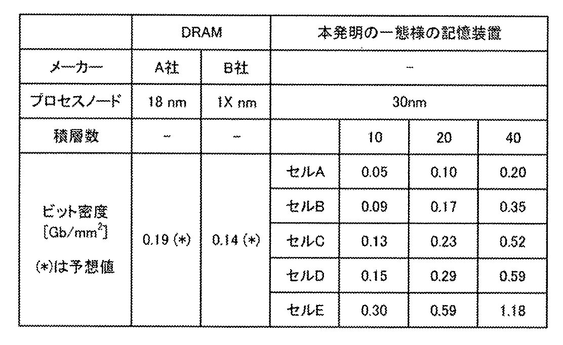
表3に、市販されているDRAMのビットコストから、本発明の一態様の半導体装置の相対ビットコストを見積もった結果を示す。なお、ビットコストの比較には、プロセスノードが1XnmのDRAMを用いた。また、本発明の一態様の半導体装置のプロセスノードは30nmとし、セルA乃至セルDにおけるメモリデバイス層の積層数を10層、20層、および40層として見積もりを行った。

なお、本実施の形態は、本明細書で示す他の実施の形態と適宜組み合わせることができる。
(実施の形態3)
本実施の形態では、上記の実施の形態で説明したOSトランジスタに用いることができる金属酸化物(以下、酸化物半導体ともいう。)について説明する。
本実施の形態では、上記の実施の形態で説明したOSトランジスタに用いることができる金属酸化物(以下、酸化物半導体ともいう。)について説明する。
金属酸化物は、少なくともインジウムまたは亜鉛を含むことが好ましい。特にインジウムおよび亜鉛を含むことが好ましい。また、それらに加えて、アルミニウム、ガリウム、イットリウム、スズなどが含まれていることが好ましい。また、ホウ素、シリコン、チタン、鉄、ニッケル、ゲルマニウム、ジルコニウム、モリブデン、ランタン、セリウム、ネオジム、ハフニウム、タンタル、タングステン、マグネシウム、コバルトなどから選ばれた一種、または複数種が含まれていてもよい。
<結晶構造の分類>
まず、酸化物半導体における、結晶構造の分類について、図21Aを用いて説明を行う。図21Aは、酸化物半導体、代表的にはIGZO(Inと、Gaと、Znと、を含む金属酸化物)の結晶構造の分類を説明する図である。
まず、酸化物半導体における、結晶構造の分類について、図21Aを用いて説明を行う。図21Aは、酸化物半導体、代表的にはIGZO(Inと、Gaと、Znと、を含む金属酸化物)の結晶構造の分類を説明する図である。
図21Aに示すように、酸化物半導体は、大きく分けて「Amorphous(無定形)」と、「Crystalline(結晶性)」と、「Crystal(結晶)」と、に分類される。また、「Amorphous」の中には、completely amorphousが含まれる。また、「Crystalline」の中には、CAAC(c−axis−aligned crystalline)、nc(nanocrystalline)、及びCAC(cloud−aligned composite)が含まれる。なお、「Crystalline」の分類には、single crystal、poly crystal、及びcompletely amorphousは除かれる。また、「Crystal」の中には、single crystal、及びpoly crystalが含まれる。
なお、図21Aに示す太枠内の構造は、「Amorphous(無定形)」と、「Crystal(結晶)」との間の中間状態であり、新しい境界領域(New crystalline phase)に属する構造である。すなわち、当該構造は、エネルギー的に不安定な「Amorphous(無定形)」や、「Crystal(結晶)」とは全く異なる構造と言い換えることができる。
なお、膜または基板の結晶構造は、X線回折(XRD:X−Ray Diffraction)スペクトルを用いて評価することができる。ここで、「Crystalline」に分類されるCAAC−IGZO膜のGIXD(Grazing−Incidence XRD)測定で得られるXRDスペクトルを図21Bに示す(縦軸は強度(Intensity)を任意単位(a.u.)で表している)。なお、GIXD法は、薄膜法またはSeemann−Bohlin法ともいう。以降、図21Bに示すGIXD測定で得られるXRDスペクトルを、単にXRDスペクトルと記す。なお、図21Bに示すCAAC−IGZO膜の組成は、In:Ga:Zn=4:2:3[原子数比]近傍である。また、図21Bに示すCAAC−IGZO膜の厚さは、500nmである。
図21Bに示すように、CAAC−IGZO膜のXRDスペクトルでは、明確な結晶性を示すピークが検出される。具体的には、CAAC−IGZO膜のXRDスペクトルでは、2θ=31°近傍に、c軸配向を示すピークが検出される。なお、図21Bに示すように、2θ=31°近傍のピークは、ピーク強度が検出された角度を軸に左右非対称である。
また、膜または基板の結晶構造は、極微電子線回折法(NBED:Nano Beam Electron Diffraction)によって観察される回折パターン(極微電子線回折パターンともいう。)にて評価することができる。CAAC−IGZO膜の回折パターンを、図21Cに示す。図21Cは、電子線を基板に対して平行に入射するNBEDによって観察される回折パターンである。なお、図21Cに示すCAAC−IGZO膜の組成は、In:Ga:Zn=4:2:3[原子数比]近傍である。また、極微電子線回折法では、プローブ径を1nmとして電子線回折が行われる。
図21Cに示すように、CAAC−IGZO膜の回折パターンでは、c軸配向を示す複数のスポットが観察される。
<<酸化物半導体の構造>>
なお、酸化物半導体は、結晶構造に着目した場合、図21Aとは異なる分類となる場合がある。例えば、酸化物半導体は、単結晶酸化物半導体と、それ以外の非単結晶酸化物半導体と、に分けられる。非単結晶酸化物半導体としては、例えば、上述のCAAC−OS、及びnc−OSがある。また、非単結晶酸化物半導体には、多結晶酸化物半導体、擬似非晶質酸化物半導体(a−like OS:amorphous−like oxide semiconductor)、非晶質酸化物半導体、などが含まれる。
なお、酸化物半導体は、結晶構造に着目した場合、図21Aとは異なる分類となる場合がある。例えば、酸化物半導体は、単結晶酸化物半導体と、それ以外の非単結晶酸化物半導体と、に分けられる。非単結晶酸化物半導体としては、例えば、上述のCAAC−OS、及びnc−OSがある。また、非単結晶酸化物半導体には、多結晶酸化物半導体、擬似非晶質酸化物半導体(a−like OS:amorphous−like oxide semiconductor)、非晶質酸化物半導体、などが含まれる。
ここで、上述のCAAC−OS、nc−OS、及びa−like OSの詳細について、説明を行う。
[CAAC−OS]
CAAC−OSは、複数の結晶領域を有し、当該複数の結晶領域はc軸が特定の方向に配向している酸化物半導体である。なお、特定の方向とは、CAAC−OS膜の厚さ方向、CAAC−OS膜の被形成面の法線方向、またはCAAC−OS膜の表面の法線方向である。また、結晶領域とは、原子配列に周期性を有する領域である。なお、原子配列を格子配列とみなすと、結晶領域とは、格子配列の揃った領域でもある。さらに、CAAC−OSは、a−b面方向において複数の結晶領域が連結する領域を有し、当該領域は歪みを有する場合がある。なお、歪みとは、複数の結晶領域が連結する領域において、格子配列の揃った領域と、別の格子配列の揃った領域と、の間で格子配列の向きが変化している箇所を指す。つまり、CAAC−OSは、c軸配向し、a−b面方向には明らかな配向をしていない酸化物半導体である。
CAAC−OSは、複数の結晶領域を有し、当該複数の結晶領域はc軸が特定の方向に配向している酸化物半導体である。なお、特定の方向とは、CAAC−OS膜の厚さ方向、CAAC−OS膜の被形成面の法線方向、またはCAAC−OS膜の表面の法線方向である。また、結晶領域とは、原子配列に周期性を有する領域である。なお、原子配列を格子配列とみなすと、結晶領域とは、格子配列の揃った領域でもある。さらに、CAAC−OSは、a−b面方向において複数の結晶領域が連結する領域を有し、当該領域は歪みを有する場合がある。なお、歪みとは、複数の結晶領域が連結する領域において、格子配列の揃った領域と、別の格子配列の揃った領域と、の間で格子配列の向きが変化している箇所を指す。つまり、CAAC−OSは、c軸配向し、a−b面方向には明らかな配向をしていない酸化物半導体である。
なお、上記複数の結晶領域のそれぞれは、1つまたは複数の微小な結晶(最大径が10nm未満である結晶)で構成される。結晶領域が1つの微小な結晶で構成されている場合、当該結晶領域の最大径は10nm未満となる。また、結晶領域が多数の微小な結晶で構成されている場合、当該結晶領域の大きさは、数十nm程度となる場合がある。
また、In−M−Zn酸化物(元素Mは、アルミニウム、ガリウム、イットリウム、スズ、チタンなどから選ばれた一種、または複数種)において、CAAC−OSは、インジウム(In)、及び酸素を有する層(以下、In層)と、元素M、亜鉛(Zn)、及び酸素を有する層(以下、(M,Zn)層)とが積層した、層状の結晶構造(層状構造ともいう)を有する傾向がある。なお、インジウムと元素Mは、互いに置換可能である。よって、(M,Zn)層にはインジウムが含まれる場合がある。また、In層には元素Mが含まれる場合がある。なお、In層にはZnが含まれる場合もある。当該層状構造は、例えば、高分解能TEM像において、格子像として観察される。
CAAC−OS膜に対し、例えば、XRD装置を用いて構造解析を行うと、θ/2θスキャンを用いたOut−of−plane XRD測定では、c軸配向を示すピークが2θ=31°またはその近傍に検出される。なお、c軸配向を示すピークの位置(2θの値)は、CAAC−OSを構成する金属元素の種類、組成などにより変動する場合がある。
また、例えば、CAAC−OS膜の電子線回折パターンにおいて、複数の輝点(スポット)が観測される。なお、あるスポットと別のスポットとは、試料を透過した入射電子線のスポット(ダイレクトスポットともいう。)を対称中心として、点対称の位置に観測される。
上記特定の方向から結晶領域を観察した場合、当該結晶領域内の格子配列は、六方格子を基本とするが、単位格子は正六角形とは限らず、非正六角形である場合がある。また、上記歪みにおいて、五角形、七角形などの格子配列を有する場合がある。なお、CAAC−OSにおいて、歪み近傍においても、明確な結晶粒界(グレインバウンダリー)を確認することはできない。即ち、格子配列の歪みによって、結晶粒界の形成が抑制されていることがわかる。これは、CAAC−OSが、a−b面方向において酸素原子の配列が稠密でないことや、金属原子が置換することで原子間の結合距離が変化することなどによって、歪みを許容することができるためと考えられる。
なお、明確な結晶粒界が確認される結晶構造は、いわゆる多結晶(polycrystal)と呼ばれる。結晶粒界は、再結合中心となり、キャリアが捕獲されトランジスタのオン電流の低下、電界効果移動度の低下などを引き起こす可能性が高い。よって、明確な結晶粒界が確認されないCAAC−OSは、トランジスタの半導体層に好適な結晶構造を有する結晶性の酸化物の一つである。なお、CAAC−OSを構成するには、Znを有する構成が好ましい。例えば、In−Zn酸化物、及びIn−Ga−Zn酸化物は、In酸化物よりも結晶粒界の発生を抑制できるため好適である。
CAAC−OSは、結晶性が高く、明確な結晶粒界が確認されない酸化物半導体である。よって、CAAC−OSは、結晶粒界に起因する電子移動度の低下が起こりにくいといえる。また、酸化物半導体の結晶性は不純物の混入や欠陥の生成などによって低下する場合があるため、CAAC−OSは不純物や欠陥(酸素欠損など)の少ない酸化物半導体ともいえる。従って、CAAC−OSを有する酸化物半導体は、物理的性質が安定する。そのため、CAAC−OSを有する酸化物半導体は熱に強く、信頼性が高い。また、CAAC−OSは、製造工程における高い温度(所謂サーマルバジェット)に対しても安定である。したがって、OSトランジスタにCAAC−OSを用いると、製造工程の自由度を広げることが可能となる。
[nc−OS]
nc−OSは、微小な領域(例えば、1nm以上10nm以下の領域、特に1nm以上3nm以下の領域)において原子配列に周期性を有する。別言すると、nc−OSは、微小な結晶を有する。なお、当該微小な結晶の大きさは、例えば、1nm以上10nm以下、特に1nm以上3nm以下であることから、当該微小な結晶をナノ結晶ともいう。また、nc−OSは、異なるナノ結晶間で結晶方位に規則性が見られない。そのため、膜全体で配向性が見られない。したがって、nc−OSは、分析方法によっては、a−like OSや非晶質酸化物半導体と区別が付かない場合がある。例えば、nc−OS膜に対し、XRD装置を用いて構造解析を行うと、θ/2θスキャンを用いたOut−of−plane XRD測定では、結晶性を示すピークが検出されない。また、nc−OS膜に対し、ナノ結晶よりも大きいプローブ径(例えば50nm以上)の電子線を用いる電子線回折(制限視野電子線回折ともいう。)を行うと、ハローパターンのような回折パターンが観測される。一方、nc−OS膜に対し、ナノ結晶の大きさと近いかナノ結晶より小さいプローブ径(例えば1nm以上30nm以下)の電子線を用いる電子線回折(ナノビーム電子線回折ともいう。)を行うと、ダイレクトスポットを中心とするリング状の領域内に複数のスポットが観測される電子線回折パターンが取得される場合がある。
nc−OSは、微小な領域(例えば、1nm以上10nm以下の領域、特に1nm以上3nm以下の領域)において原子配列に周期性を有する。別言すると、nc−OSは、微小な結晶を有する。なお、当該微小な結晶の大きさは、例えば、1nm以上10nm以下、特に1nm以上3nm以下であることから、当該微小な結晶をナノ結晶ともいう。また、nc−OSは、異なるナノ結晶間で結晶方位に規則性が見られない。そのため、膜全体で配向性が見られない。したがって、nc−OSは、分析方法によっては、a−like OSや非晶質酸化物半導体と区別が付かない場合がある。例えば、nc−OS膜に対し、XRD装置を用いて構造解析を行うと、θ/2θスキャンを用いたOut−of−plane XRD測定では、結晶性を示すピークが検出されない。また、nc−OS膜に対し、ナノ結晶よりも大きいプローブ径(例えば50nm以上)の電子線を用いる電子線回折(制限視野電子線回折ともいう。)を行うと、ハローパターンのような回折パターンが観測される。一方、nc−OS膜に対し、ナノ結晶の大きさと近いかナノ結晶より小さいプローブ径(例えば1nm以上30nm以下)の電子線を用いる電子線回折(ナノビーム電子線回折ともいう。)を行うと、ダイレクトスポットを中心とするリング状の領域内に複数のスポットが観測される電子線回折パターンが取得される場合がある。
[a−like OS]
a−like OSは、nc−OSと非晶質酸化物半導体との間の構造を有する酸化物半導体である。a−like OSは、鬆又は低密度領域を有する。即ち、a−like OSは、nc−OS及びCAAC−OSと比べて、結晶性が低い。また、a−like OSは、nc−OS及びCAAC−OSと比べて、膜中の水素濃度が高い。
a−like OSは、nc−OSと非晶質酸化物半導体との間の構造を有する酸化物半導体である。a−like OSは、鬆又は低密度領域を有する。即ち、a−like OSは、nc−OS及びCAAC−OSと比べて、結晶性が低い。また、a−like OSは、nc−OS及びCAAC−OSと比べて、膜中の水素濃度が高い。
<<酸化物半導体の構成>>
次に、上述のCAC−OSの詳細について、説明を行う。なお、CAC−OSは材料構成に関する。
次に、上述のCAC−OSの詳細について、説明を行う。なお、CAC−OSは材料構成に関する。
[CAC−OS]
CAC−OSとは、例えば、金属酸化物を構成する元素が、0.5nm以上10nm以下、好ましくは、1nm以上3nm以下、またはその近傍のサイズで偏在した材料の一構成である。なお、以下では、金属酸化物において、一つまたは複数の金属元素が偏在し、該金属元素を有する領域が、0.5nm以上10nm以下、好ましくは、1nm以上3nm以下、またはその近傍のサイズで混合した状態をモザイク状、またはパッチ状ともいう。
CAC−OSとは、例えば、金属酸化物を構成する元素が、0.5nm以上10nm以下、好ましくは、1nm以上3nm以下、またはその近傍のサイズで偏在した材料の一構成である。なお、以下では、金属酸化物において、一つまたは複数の金属元素が偏在し、該金属元素を有する領域が、0.5nm以上10nm以下、好ましくは、1nm以上3nm以下、またはその近傍のサイズで混合した状態をモザイク状、またはパッチ状ともいう。
さらに、CAC−OSとは、第1の領域と、第2の領域と、に材料が分離することでモザイク状となり、当該第1の領域が、膜中に分布した構成(以下、クラウド状ともいう。)である。つまり、CAC−OSは、当該第1の領域と、当該第2の領域とが、混合している構成を有する複合金属酸化物である。
ここで、In−Ga−Zn酸化物におけるCAC−OSを構成する金属元素に対するIn、Ga、およびZnの原子数比のそれぞれを、[In]、[Ga]、および[Zn]と表記する。例えば、In−Ga−Zn酸化物におけるCAC−OSにおいて、第1の領域は、[In]が、CAC−OS膜の組成における[In]よりも大きい領域である。また、第2の領域は、[Ga]が、CAC−OS膜の組成における[Ga]よりも大きい領域である。または、例えば、第1の領域は、[In]が、第2の領域における[In]よりも大きく、且つ、[Ga]が、第2の領域における[Ga]よりも小さい領域である。また、第2の領域は、[Ga]が、第1の領域における[Ga]よりも大きく、且つ、[In]が、第1の領域における[In]よりも小さい領域である。
具体的には、上記第1の領域は、インジウム酸化物、インジウム亜鉛酸化物などが主成分である領域である。また、上記第2の領域は、ガリウム酸化物、ガリウム亜鉛酸化物などが主成分である領域である。つまり、上記第1の領域を、Inを主成分とする領域と言い換えることができる。また、上記第2の領域を、Gaを主成分とする領域と言い換えることができる。
なお、上記第1の領域と、上記第2の領域とは、明確な境界が観察できない場合がある。
例えば、In−Ga−Zn酸化物におけるCAC−OSでは、エネルギー分散型X線分光法(EDX:Energy Dispersive X−ray spectroscopy)を用いて取得したEDXマッピングにより、Inを主成分とする領域(第1の領域)と、Gaを主成分とする領域(第2の領域)とが、偏在し、混合している構造を有することが確認できる。
CAC−OSをトランジスタに用いる場合、第1の領域に起因する導電性と、第2の領域に起因する絶縁性とが、相補的に作用することにより、スイッチングさせる機能(On/Offさせる機能)をCAC−OSに付与することができる。つまり、CAC−OSとは、材料の一部では導電性の機能と、材料の一部では絶縁性の機能とを有し、材料の全体では半導体としての機能を有する。導電性の機能と絶縁性の機能とを分離させることで、双方の機能を最大限に高めることができる。よって、CAC−OSをトランジスタに用いることで、高いオン電流(Ion)、高い電界効果移動度(μ)、および良好なスイッチング動作を実現することができる。
酸化物半導体は、多様な構造をとり、それぞれが異なる特性を有する。本発明の一態様の酸化物半導体は、非晶質酸化物半導体、多結晶酸化物半導体、a−like OS、CAC−OS、nc−OS、CAAC−OSのうち、二種以上を有していてもよい。
<酸化物半導体を有するトランジスタ>
続いて、上記酸化物半導体をトランジスタに用いる場合について説明する。
続いて、上記酸化物半導体をトランジスタに用いる場合について説明する。
上記酸化物半導体をトランジスタに用いることで、高い電界効果移動度のトランジスタを実現することができる。また、信頼性の高いトランジスタを実現することができる。
トランジスタには、キャリア濃度の低い酸化物半導体を用いることが好ましい。例えば、酸化物半導体のキャリア濃度は1×1017cm−3以下、好ましくは1×1015cm−3以下、さらに好ましくは1×1013cm−3以下、より好ましくは1×1011cm−3以下、さらに好ましくは1×1010cm−3未満であり、1×10⁻⁹cm−3以上である。なお、酸化物半導体膜のキャリア濃度を低くする場合においては、酸化物半導体膜中の不純物濃度を低くし、欠陥準位密度を低くすればよい。本明細書等において、不純物濃度が低く、欠陥準位密度の低いことを高純度真性又は実質的に高純度真性と言う。なお、キャリア濃度の低い酸化物半導体を、高純度真性又は実質的に高純度真性な酸化物半導体と呼ぶ場合がある。
また、高純度真性又は実質的に高純度真性である酸化物半導体膜は、欠陥準位密度が低いため、トラップ準位密度も低くなる場合がある。
また、酸化物半導体のトラップ準位に捕獲された電荷は、消失するまでに要する時間が長く、あたかも固定電荷のように振る舞うことがある。そのため、トラップ準位密度の高い酸化物半導体にチャネル形成領域が形成されるトランジスタは、電気特性が不安定となる場合がある。
従って、トランジスタの電気特性を安定にするためには、酸化物半導体中の不純物濃度を低減することが有効である。また、酸化物半導体中の不純物濃度を低減するためには、近接する膜中の不純物濃度も低減することが好ましい。不純物としては、水素、窒素、アルカリ金属、アルカリ土類金属、鉄、ニッケル、シリコン等がある。
<不純物>
ここで、酸化物半導体中における各不純物の影響について説明する。
ここで、酸化物半導体中における各不純物の影響について説明する。
酸化物半導体において、第14族元素の一つであるシリコンや炭素が含まれると、酸化物半導体において欠陥準位が形成される。このため、酸化物半導体におけるシリコンや炭素の濃度と、酸化物半導体との界面近傍のシリコンや炭素の濃度(二次イオン質量分析法(SIMS:Secondary Ion Mass Spectrometry)により得られる濃度)を、2×10¹⁸atoms/cm3以下、好ましくは2×1017atoms/cm3以下とする。
また、酸化物半導体にアルカリ金属又はアルカリ土類金属が含まれると、欠陥準位を形成し、キャリアを生成する場合がある。従って、アルカリ金属又はアルカリ土類金属が含まれている酸化物半導体を用いたトランジスタはノーマリーオン特性となりやすい。このため、SIMSにより得られる酸化物半導体中のアルカリ金属又はアルカリ土類金属の濃度を、1×10¹⁸atoms/cm3以下、好ましくは2×1016atoms/cm3以下にする。
また、酸化物半導体において、窒素が含まれると、キャリアである電子が生じ、キャリア濃度が増加し、n型化しやすい。この結果、窒素が含まれている酸化物半導体を半導体に用いたトランジスタはノーマリーオン特性となりやすい。または、酸化物半導体において、窒素が含まれると、トラップ準位が形成される場合がある。この結果、トランジスタの電気特性が不安定となる場合がある。このため、SIMSにより得られる酸化物半導体中の窒素濃度を、5×10¹⁹atoms/cm3未満、好ましくは5×1018atoms/cm3以下、より好ましくは1×1018atoms/cm3以下、さらに好ましくは5×1017atoms/cm3以下にする。
また、酸化物半導体に含まれる水素は、金属原子と結合する酸素と反応して水になるため、酸素欠損を形成する場合がある。該酸素欠損に水素が入ることで、キャリアである電子が生成される場合がある。また、水素の一部が金属原子と結合する酸素と結合して、キャリアである電子を生成することがある。従って、水素が含まれている酸化物半導体を用いたトランジスタはノーマリーオン特性となりやすい。このため、酸化物半導体中の水素はできる限り低減されていることが好ましい。具体的には、酸化物半導体において、SIMSにより得られる水素濃度を、1×10²⁰atoms/cm3未満、好ましくは1×1019atoms/cm3未満、より好ましくは5×1018atoms/cm3未満、さらに好ましくは1×1018atoms/cm3未満にする。
不純物が十分に低減された酸化物半導体をトランジスタのチャネル形成領域に用いることで、安定した電気特性を付与することができる。
なお、本実施の形態は、本明細書で示す他の実施の形態と適宜組み合わせることができる。
(実施の形態4)
本実施の形態では、上記の実施の形態の記憶装置100に備えることができるコントロールロジック回路561、行駆動回路562、列駆動回路563および出力回路564について説明する。
本実施の形態では、上記の実施の形態の記憶装置100に備えることができるコントロールロジック回路561、行駆動回路562、列駆動回路563および出力回路564について説明する。
図22は、メモリ装置として機能する半導体装置の構成例を示すブロック図である。半導体装置510Eは、周辺回路580、およびメモリセルアレイ570を有する。周辺回路580は、コントロールロジック回路561、行駆動回路562、列駆動回路563、出力回路564を有する。
メモリセルアレイ570は、複数のメモリセル542を有する。行駆動回路562は、ロウデコーダ571およびワード線ドライバ回路572を有する。列駆動回路563は、カラムデコーダ581、プリチャージ回路582、増幅回路583、および書き込み回路584を有する。プリチャージ回路582は、例えば、実施の形態1で説明した配線GBL、配線LBLなどをプリチャージする機能を有する。増幅回路583は、例えば、配線GBL、配線LBLなどから読み出されたデータ信号を増幅する機能を有する。増幅されたデータ信号は、出力回路564を介して、デジタルのデータ信号RDATAとして半導体装置510Eの外部に出力される。
半導体装置510Eには、外部から電源電圧として低電源電圧(VSS)、周辺回路580用の高電源電圧(VDD)、メモリセルアレイ570用の高電源電圧(VIL)が供給される。
また半導体装置510Eには、制御信号(CE、WE、RE)、アドレス信号ADDR、データ信号WDATAが外部から入力される。アドレス信号ADDRは、ロウデコーダ571およびカラムデコーダ581に入力され、WDATAは書き込み回路584に入力される。
コントロールロジック回路561は、外部からの入力信号(CE、WE、RE)を処理して、ロウデコーダ571、カラムデコーダ581の制御信号を生成する。CEは、チップイネーブル信号であり、WEは、書き込みイネーブル信号であり、REは、読み出しイネーブル信号である。コントロールロジック回路561が処理する信号は、これに限定されるものではなく、必要に応じて、他の制御信号を入力すればよい。例えば不良ビットを判定するための制御信号を入力し、特定のメモリセルのアドレスから読み出されるデータ信号を不良ビットとして特定してもよい。
なお、上述の各回路あるいは各信号は、必要に応じて、適宜、取捨することができる。
一般に、コンピュータなどの半導体装置では、用途に応じて様々な記憶装置(メモリ)が用いられる。図23に、各種の記憶装置を階層ごとに示す。上層に位置する記憶装置ほど速いアクセス速度が求められ、下層に位置する記憶装置ほど大きな記憶容量と高い記録密度が求められる。図23では、最上層から順に、CPUなどの演算処理装置にレジスタとして混載されるメモリ、SRAM(Static Random Access Memory)、DRAM(Dynamic Random Access Memory)、3D NANDメモリを示している。
CPUなどの演算処理装置にレジスタとして混載されるメモリは、演算結果の一時保存などに用いられるため、演算処理装置からのアクセス頻度が高い。よって、記憶容量よりも速い動作速度が求められる。また、レジスタは演算処理装置の設定情報などを保持する機能も有する。
SRAMは、例えばキャッシュに用いられる。キャッシュは、メインメモリに保持されている情報の一部を複製して保持する機能を有する。使用頻繁が高いデータをキャッシュに複製しておくことで、データへのアクセス速度を高めることができる。
DRAMは、例えばメインメモリに用いられる。メインメモリは、ストレージから読み出されたプログラムやデータを保持する機能を有する。DRAMの記録密度は、おおよそ0.1乃至0.3Gbit/mm2である。
3D NANDメモリは、例えばストレージに用いられる。ストレージは、長期保存が必要なデータや、演算処理装置で使用する各種のプログラムなどを保持する機能を有する。よって、ストレージには動作速度よりも大きな記憶容量と高い記録密度が求められる。ストレージに用いられる記憶装置の記録密度は、おおよそ0.6乃至6.0Gbit/mm2である。
本発明の一態様の記憶装置として機能する半導体装置は、動作速度が速く、長期間のデータ保持が可能である。本発明の一態様の半導体装置は、キャッシュが位置する階層とメインメモリが位置する階層の双方を含む境界領域901に位置する半導体装置として好適に用いることができる。また、本発明の一態様の半導体装置は、メインメモリが位置する階層とストレージが位置する階層の双方を含む境界領域902に位置する半導体装置として好適に用いることができる。
(実施の形態5)
本実施の形態は、上記実施の形態に示す半導体装置などが形成された半導体ウェハ、及び当該半導体装置が組み込まれた電子部品の一例を示す。
本実施の形態は、上記実施の形態に示す半導体装置などが形成された半導体ウェハ、及び当該半導体装置が組み込まれた電子部品の一例を示す。
<半導体ウェハ>
初めに、半導体装置などが形成された半導体ウェハの例を、図24Aを用いて説明する。
初めに、半導体装置などが形成された半導体ウェハの例を、図24Aを用いて説明する。
図24Aに示す半導体ウェハ4800は、ウェハ4801と、ウェハ4801の上面に設けられた複数の回路部4802と、を有する。なお、ウェハ4801の上面において、回路部4802の無い部分は、スペーシング4803であり、ダイシング用の領域である。
半導体ウェハ4800は、ウェハ4801の表面に対して、前工程によって複数の回路部4802を形成することで作製することができる。また、その後に、ウェハ4801の複数の回路部4802が形成された反対側の面を研削して、ウェハ4801の薄膜化してもよい。この工程により、ウェハ4801の反りなどを低減し、部品としての小型化を図ることができる。
次の工程としては、ダイシング工程が行われる。ダイシングは、一点鎖線で示したスクライブラインSCL1及びスクライブラインSCL2(ダイシングライン、又は切断ラインと呼ぶ場合がある)に沿って行われる。なお、スペーシング4803は、ダイシング工程を容易に行うために、複数のスクライブラインSCL1が平行になるように設け、複数のスクライブラインSCL2が平行になるように設け、スクライブラインSCL1とスクライブラインSCL2が垂直になるように設けるのが好ましい。
ダイシング工程を行うことにより、図24Bに示すようなチップ4800aを、半導体ウェハ4800から切り出すことができる。チップ4800aは、ウェハ4801aと、回路部4802と、スペーシング4803aと、を有する。なお、スペーシング4803aは、極力小さくなるようにするのが好ましい。この場合、隣り合う回路部4802の間のスペーシング4803の幅が、スクライブラインSCL1の切りしろと、又はスクライブラインSCL2の切りしろとほぼ同等の長さであればよい。
なお、本発明の一態様の素子基板の形状は、図24Aに図示した半導体ウェハ4800の形状に限定されない。例えば、矩形の形状の半導体ウェハあってもよい。素子基板の形状は、素子の作製工程、及び素子を作製するための装置に応じて、適宜変更することができる。
<電子部品>
図24Cに電子部品4700および電子部品4700が実装された基板(実装基板4704)の斜視図を示す。図24Cに示す電子部品4700は、モールド4711内にチップ4800aを有している。なお、図24Cに示すチップ4800aには、回路部4802が積層された構成を示している。つまり、回路部4802として、上記の実施の形態で説明した半導体装置を適用することができる。図24Cは、電子部品4700の内部を示すために、一部を省略している。電子部品4700は、モールド4711の外側にランド4712を有する。ランド4712は電極パッド4713と電気的に接続され、電極パッド4713はチップ4800aとワイヤ4714によって電気的に接続されている。電子部品4700は、例えばプリント基板4702に実装される。このような電子部品が複数組み合わされて、それぞれがプリント基板4702上で電気的に接続されることで実装基板4704が完成する。
図24Cに電子部品4700および電子部品4700が実装された基板(実装基板4704)の斜視図を示す。図24Cに示す電子部品4700は、モールド4711内にチップ4800aを有している。なお、図24Cに示すチップ4800aには、回路部4802が積層された構成を示している。つまり、回路部4802として、上記の実施の形態で説明した半導体装置を適用することができる。図24Cは、電子部品4700の内部を示すために、一部を省略している。電子部品4700は、モールド4711の外側にランド4712を有する。ランド4712は電極パッド4713と電気的に接続され、電極パッド4713はチップ4800aとワイヤ4714によって電気的に接続されている。電子部品4700は、例えばプリント基板4702に実装される。このような電子部品が複数組み合わされて、それぞれがプリント基板4702上で電気的に接続されることで実装基板4704が完成する。
図24Dに電子部品4730の斜視図を示す。電子部品4730は、SiP(System in package)またはMCM(Multi Chip Module)の一例である。電子部品4730は、パッケージ基板4732(プリント基板)上にインターポーザ4731が設けられ、インターポーザ4731上に半導体装置4735、および複数の半導体装置4710が設けられている。
電子部品4730では、半導体装置4710を有する。半導体装置4710としては、例えば、上記実施の形態で説明した半導体装置、広帯域メモリ(HBM:High Bandwidth Memory)などとすることができる。また、半導体装置4735には、CPU、GPU、FPGA、記憶装置などの集積回路(半導体装置)を用いることができる。
パッケージ基板4732は、セラミック基板、プラスチック基板、またはガラスエポキシ基板などを用いることができる。インターポーザ4731は、シリコンインターポーザ、樹脂インターポーザなどを用いることができる。
インターポーザ4731は、複数の配線を有し、端子ピッチの異なる複数の集積回路を電気的に接続する機能を有する。複数の配線は、単層または多層で設けられる。また、インターポーザ4731は、インターポーザ4731上に設けられた集積回路をパッケージ基板4732に設けられた電極と電気的に接続する機能を有する。これらのことから、インターポーザを「再配線基板」または「中間基板」と呼ぶ場合がある。また、インターポーザ4731に貫通電極を設けて、当該貫通電極を用いて集積回路とパッケージ基板4732を電気的に接続する場合もある。また、シリコンインターポーザでは、貫通電極として、TSV(Through Silicon Via)を用いることも出来る。
インターポーザ4731としてシリコンインターポーザを用いることが好ましい。シリコンインターポーザでは能動素子を設ける必要が無いため、集積回路よりも低コストで作製することができる。一方で、シリコンインターポーザの配線形成は半導体プロセスで行なうことができるため、樹脂インターポーザでは難しい微細配線の形成が容易である。
HBMでは、広いメモリバンド幅を実現するために多くの配線を接続する必要がある。このため、HBMを実装するインターポーザには、微細かつ高密度の配線形成が求められる。よって、HBMを実装するインターポーザには、シリコンインターポーザを用いることが好ましい。
また、シリコンインターポーザを用いたSiPやMCMなどでは、集積回路とインターポーザ間の膨張係数の違いによる信頼性の低下が生じにくい。また、シリコンインターポーザは表面の平坦性が高いため、シリコンインターポーザ上に設ける集積回路とシリコンインターポーザ間の接続不良が生じにくい。特に、インターポーザ上に複数の集積回路を横に並べて配置する2.5Dパッケージ(2.5次元実装)では、シリコンインターポーザを用いることが好ましい。
また、電子部品4730と重ねてヒートシンク(放熱板)を設けてもよい。ヒートシンクを設ける場合は、インターポーザ4731上に設ける集積回路の高さを揃えることが好ましい。例えば、本実施の形態に示す電子部品4730では、半導体装置4710と半導体装置4735の高さを揃えることが好ましい。
電子部品4730を他の基板に実装するため、パッケージ基板4732の底部に電極4733を設けてもよい。図24Dでは、電極4733を半田ボールで形成する例を示している。パッケージ基板4732の底部に半田ボールをマトリクス状に設けることで、BGA(Ball Grid Array)実装を実現できる。また、電極4733を導電性のピンで形成してもよい。パッケージ基板4732の底部に導電性のピンをマトリクス状に設けることで、PGA(Pin Grid Array)実装を実現できる。
電子部品4730は、BGAおよびPGAに限らず様々な実装方法を用いて他の基板に実装することができる。例えば、SPGA(Staggered Pin Grid Array)、LGA(Land Grid Array)、QFP(Quad Flat Package)、QFJ(Quad Flat J−leaded package)、またはQFN(Quad Flat Non−leaded package)などの実装方法を用いることができる。
なお、本実施の形態は、本明細書で示す他の実施の形態と適宜組み合わせることができる。
(実施の形態6)
本実施の形態では、上記実施の形態で説明した半導体装置を有する電子機器の一例について説明する。なお、図25A乃至図25J、図26A乃至図26Eには、当該半導体装置を有する電子部品4700が各電子機器に含まれている様子を図示している。
本実施の形態では、上記実施の形態で説明した半導体装置を有する電子機器の一例について説明する。なお、図25A乃至図25J、図26A乃至図26Eには、当該半導体装置を有する電子部品4700が各電子機器に含まれている様子を図示している。
[携帯電話]
図25Aに示す情報端末5500は、情報端末の一種である携帯電話(スマートフォン)である。情報端末5500は、筐体5510と、表示部5511と、を有しており、入力用インターフェースとして、タッチパネルが表示部5511に備えられ、ボタンが筐体5510に備えられている。
図25Aに示す情報端末5500は、情報端末の一種である携帯電話(スマートフォン)である。情報端末5500は、筐体5510と、表示部5511と、を有しており、入力用インターフェースとして、タッチパネルが表示部5511に備えられ、ボタンが筐体5510に備えられている。
情報端末5500は、上記実施の形態で説明した半導体装置を適用することで、アプリケーションの実行時に生成される一時的なファイル(例えば、ウェブブラウザの使用時のキャッシュなど)を保持することができる。
[ウェアラブル端末]
また、図25Bには、ウェアラブル端末の一例として情報端末5900が図示されている。情報端末5900は、筐体5901、表示部5902、操作ボタン5903、操作子5904、バンド5905などを有する。
また、図25Bには、ウェアラブル端末の一例として情報端末5900が図示されている。情報端末5900は、筐体5901、表示部5902、操作ボタン5903、操作子5904、バンド5905などを有する。
ウェアラブル端末は、先述した情報端末5500と同様に、上記実施の形態で説明した半導体装置を適用することで、アプリケーションの実行時に生成される一時的なファイルを保持することができる。
[情報端末]
また、図25Cには、デスクトップ型情報端末5300が図示されている。デスクトップ型情報端末5300は、情報端末の本体5301と、ディスプレイ5302と、キーボード5303と、を有する。
また、図25Cには、デスクトップ型情報端末5300が図示されている。デスクトップ型情報端末5300は、情報端末の本体5301と、ディスプレイ5302と、キーボード5303と、を有する。
デスクトップ型情報端末5300は、先述した情報端末5500と同様に、上記実施の形態で説明した半導体装置を適用することで、アプリケーションの実行時に生成される一時的なファイルを保持することができる。
なお、上述では、電子機器としてスマートフォン、ウェアラブル端末、及びデスクトップ用情報端末を例として、それぞれ図25A、及び図25Cに図示したが、スマートフォン、ウェアラブル端末、及びデスクトップ用情報端末以外の情報端末を適用することができる。スマートフォン、ウェアラブル端末、及びデスクトップ用情報端末以外の情報端末としては、例えば、PDA(Personal Digital Assistant)、ノート型情報端末、ワークステーションなどが挙げられる。
[電化製品]
また、図25Dには、電化製品の一例として電気冷凍冷蔵庫5800が図示されている。電気冷凍冷蔵庫5800は、筐体5801、冷蔵室用扉5802、冷凍室用扉5803等を有する。
また、図25Dには、電化製品の一例として電気冷凍冷蔵庫5800が図示されている。電気冷凍冷蔵庫5800は、筐体5801、冷蔵室用扉5802、冷凍室用扉5803等を有する。
電気冷凍冷蔵庫5800に上記実施の形態で説明した半導体装置を適用することによって、電気冷凍冷蔵庫5800を、例えば、IoT(Internet of Things)として利用することができる。IoTを利用することによって、電気冷凍冷蔵庫5800は、電気冷凍冷蔵庫5800に保存されている食材、その食材の消費期限などの情報を、インターネットなどを通じて、上述したような情報端末などに送受信することができる。また、電気冷凍冷蔵庫5800は、当該情報を送信する際に、当該情報を一時ファイルとして、当該半導体装置に保持することができる。
本一例では、電化製品として電気冷凍冷蔵庫について説明したが、その他の電化製品としては、例えば、掃除機、電子レンジ、電子オーブン、炊飯器、湯沸かし器、IH調理器、ウォーターサーバ、エアーコンディショナーを含む冷暖房器具、洗濯機、乾燥機、オーディオビジュアル機器などが挙げられる。
[ゲーム機]
また、図25Eには、ゲーム機の一例である携帯ゲーム機5200が図示されている。携帯ゲーム機5200は、筐体5201、表示部5202、ボタン5203等を有する。
また、図25Eには、ゲーム機の一例である携帯ゲーム機5200が図示されている。携帯ゲーム機5200は、筐体5201、表示部5202、ボタン5203等を有する。
更に、図25Fには、ゲーム機の一例である据え置き型ゲーム機7500が図示されている。据え置き型ゲーム機7500は、本体7520と、コントローラ7522を有する。なお、本体7520には、無線または有線によってコントローラ7522を接続することができる。また、図25Fには示していないが、コントローラ7522は、ゲームの画像を表示する表示部、ボタン以外の入力インターフェースとなるタッチパネルやスティック、回転式つまみ、スライド式つまみなどを備えることができる。また、コントローラ7522は、図25Fに示す形状に限定されず、ゲームのジャンルに応じて、コントローラ7522の形状を様々に変更してもよい。例えば、FPS(First Person Shooter)などのシューティングゲームでは、トリガーをボタンとし、銃を模した形状のコントローラを用いることができる。また、例えば、音楽ゲームなどでは、楽器、音楽機器などを模した形状のコントローラを用いることができる。更に、据え置き型ゲーム機は、コントローラを使わず、代わりにカメラ、深度センサ、マイクロフォンなどを備えて、ゲームプレイヤーのジェスチャー、及び/又は音声によって操作する形式としてもよい。
また、上述したゲーム機の映像は、テレビジョン装置、パーソナルコンピュータ用ディスプレイ、ゲーム用ディスプレイ、ヘッドマウントディスプレイなどの表示装置によって、出力することができる。
携帯ゲーム機5200に上記実施の形態で説明した半導体装置を適用することによって、低消費電力の携帯ゲーム機5200を実現することができる。また、低消費電力により、回路からの発熱を低減することができるため、発熱によるその回路自体、周辺回路、及びモジュールへの影響を少なくすることができる。
更に、携帯ゲーム機5200に上記実施の形態で説明した半導体装置を適用することによって、ゲームの実行中に発生する演算に必要な一時ファイルなどの保持をおこなうことができる。
図25E、及び図25Fでは、ゲーム機の一例として携帯ゲーム機を図示しているが、本発明の一態様の電子機器はこれに限定されない。本発明の一態様の電子機器としては、例えば、家庭用の据え置き型ゲーム機、娯楽施設(ゲームセンター、遊園地など)に設置されるアーケードゲーム機、スポーツ施設に設置されるバッティング練習用の投球マシンなどが挙げられる。
[移動体]
上記実施の形態で説明した半導体装置は、移動体である自動車、及び自動車の運転席周辺に適用することができる。
上記実施の形態で説明した半導体装置は、移動体である自動車、及び自動車の運転席周辺に適用することができる。
図25Gには移動体の一例である自動車5700が図示されている。
自動車5700の運転席周辺には、スピードメーターやタコメーター、走行距離、燃料計、ギア状態、エアコンの設定などを表示することで、様々な情報を提供するインストゥルメントパネルが備えられている。また、運転席周辺には、それらの情報を示す表示装置が備えられていてもよい。
自動車5700の外側に設けられた撮像装置(図示しない。)からの映像を当該表示装置に映し出すことによって、ピラーなどで遮られた視界、運転席の死角などを補うことができ、安全性を高めることができる。
上記実施の形態で説明した半導体装置は、情報を一時的に保持することができるため、例えば、当該コンピュータを自動車5700の自動運転システムや当該コンピュータを道路案内、危険予測などを行うシステムなどにおける、必要な一時的な情報の保持に用いることができる。当該表示装置には、道路案内、危険予測などの一時的な情報を表示する構成としてもよい。また、自動車5700に備え付けられたドライビングレコーダの映像を保持する構成としてもよい。
なお、上述では、移動体の一例として自動車について説明しているが、移動体は自動車に限定されない。例えば、移動体としては、電車、モノレール、船、飛行体(ヘリコプター、無人航空機(ドローン)、飛行機、ロケット)なども挙げることができる。
[カメラ]
上記実施の形態で説明した半導体装置は、カメラに適用することができる。
上記実施の形態で説明した半導体装置は、カメラに適用することができる。
図25Hには、撮像装置の一例であるデジタルカメラ6240が図示されている。デジタルカメラ6240は、筐体6241、表示部6242、操作ボタン6243、シャッターボタン6244等を有し、また、デジタルカメラ6240には、着脱可能なレンズ6246が取り付けられている。なお、ここではデジタルカメラ6240を、レンズ6246を筐体6241から取り外して交換することが可能な構成としたが、レンズ6246と筐体6241とが一体となっていてもよい。また、デジタルカメラ6240は、ストロボ装置や、ビューファインダー等を別途装着することができる構成としてもよい。
デジタルカメラ6240に上記実施の形態で説明した半導体装置を適用することによって、低消費電力のデジタルカメラ6240を実現することができる。また、低消費電力により、回路からの発熱を低減することができるため、発熱によるその回路自体、周辺回路、及びモジュールへの影響を少なくすることができる。
[ビデオカメラ]
上記実施の形態で説明した半導体装置は、ビデオカメラに適用することができる。
上記実施の形態で説明した半導体装置は、ビデオカメラに適用することができる。
図25Iには、撮像装置の一例であるビデオカメラ6300が図示されている。ビデオカメラ6300は、第1筐体6301、第2筐体6302、表示部6303、操作キー6304、レンズ6305、接続部6306等を有する。操作キー6304及びレンズ6305は第1筐体6301に設けられており、表示部6303は第2筐体6302に設けられている。そして、第1筐体6301と第2筐体6302とは、接続部6306により接続されており、第1筐体6301と第2筐体6302の間の角度は、接続部6306により変更が可能である。表示部6303における映像を、接続部6306における第1筐体6301と第2筐体6302との間の角度に従って切り替える構成としてもよい。
ビデオカメラ6300で撮影した映像を記録する際、データの記録形式に応じたエンコードを行う必要がある。上述した半導体装置を利用することによって、ビデオカメラ6300は、エンコードの際に発生する一時的なファイルの保持を行うことができる。
[ICD]
上記実施の形態で説明した半導体装置は、植え込み型除細動器(ICD)に適用することができる。
上記実施の形態で説明した半導体装置は、植え込み型除細動器(ICD)に適用することができる。
図25Jは、ICDの一例を示す断面模式図である。ICD本体5400は、バッテリー5401と、電子部品4700と、レギュレータと、制御回路と、アンテナ5404と、右心房へのワイヤ5402、右心室へのワイヤ5403とを少なくとも有している。
ICD本体5400は手術により体内に設置され、二本のワイヤは、人体の鎖骨下静脈5405及び上大静脈5406を通過させて一方のワイヤ先端が右心室、もう一方のワイヤ先端が右心房に設置されるようにする。
ICD本体5400は、ペースメーカのとしての機能を有し、心拍数が規定の範囲から外れた場合に心臓に対してペーシングを行う。また、ペーシングによって心拍数が改善しない場合(速い心室頻拍や心室細動など)、電気ショックによる治療が行われる。
ICD本体5400は、ペーシング及び電気ショックを適切に行うため、心拍数を常に監視する必要がある。そのため、ICD本体5400は、心拍数を検知するためのセンサを有する。また、ICD本体5400は、当該センサなどによって取得した心拍数のデータ、ペーシングによる治療を行った回数、時間などを電子部品4700に記憶することができる。
また、アンテナ5404で電力が受信でき、その電力はバッテリー5401に充電される。また、ICD本体5400は複数のバッテリーを有することにより、安全性を高くすることができる。具体的には、ICD本体5400の一部のバッテリーが使えなくなったとしても残りのバッテリーが機能させることができるため、補助電源としても機能する。
また、電力を受信できるアンテナ5404とは別に、生理信号を送信できるアンテナを有していてもよく、例えば、脈拍、呼吸数、心拍数、体温などの生理信号を外部のモニタ装置で確認できるような心臓活動を監視するシステムを構成してもよい。
[PC用の拡張デバイス]
上記実施の形態で説明した半導体装置は、PC(Personal Computer)などの計算機、情報端末用の拡張デバイスに適用することができる。
上記実施の形態で説明した半導体装置は、PC(Personal Computer)などの計算機、情報端末用の拡張デバイスに適用することができる。
図26Aは、当該拡張デバイスの一例として、持ち運びのできる、情報の記憶が可能なチップが搭載された、PCに外付けする拡張デバイス6100を示している。拡張デバイス6100は、例えば、USB(Universal Serial Bus)などでPCに接続することで、当該チップによる情報の記憶を行うことができる。なお、図26Aは、持ち運びが可能な形態の拡張デバイス6100を図示しているが、本発明の一態様に係る拡張デバイスは、これに限定されず、例えば、冷却用ファンなどを搭載した比較的大きい形態の拡張デバイスとしてもよい。
拡張デバイス6100は、筐体6101、キャップ6102、USBコネクタ6103及び基板6104を有する。基板6104は、筐体6101に収納されている。基板6104には、上記実施の形態で説明した半導体装置などを駆動する回路が設けられている。例えば、基板6104には、電子部品4700、コントローラチップ6106が取り付けられている。USBコネクタ6103は、外部装置と接続するためのインターフェースとして機能する。
[SDカード]
上記実施の形態で説明した半導体装置は、情報端末やデジタルカメラなどの電子機器に取り付けが可能なSDカードに適用することができる。
上記実施の形態で説明した半導体装置は、情報端末やデジタルカメラなどの電子機器に取り付けが可能なSDカードに適用することができる。
図26BはSDカードの外観の模式図であり、図26Cは、SDカードの内部構造の模式図である。SDカード5110は、筐体5111、コネクタ5112及び基板5113を有する。コネクタ5112が外部装置と接続するためのインターフェースとして機能する。基板5113は筐体5111に収納されている。基板5113には、記憶装置及び記憶装置を駆動する回路が設けられている。例えば、基板5113には、電子部品4700、コントローラチップ5115が取り付けられている。なお、電子部品4700とコントローラチップ5115とのそれぞれの回路構成は、上述の記載に限定せず、状況に応じて、適宜回路構成を変更してもよい。例えば、電子部品に備えられている書き込み回路、ロードライバ、読み出し回路などは、電子部品4700でなく、コントローラチップ5115に組み込んだ構成としてもよい。
基板5113の裏面側にも電子部品4700を設けることで、SDカード5110の容量を増やすことができる。また、無線通信機能を備えた無線チップを基板5113に設けてもよい。これによって、外部装置とSDカード5110との間で無線通信を行うことができ、電子部品4700のデータの読み出し、書き込みが可能となる。
[SSD]
上記実施の形態で説明した半導体装置は、情報端末など電子機器に取り付けが可能なSSD(Solid State Drive)に適用することができる。
上記実施の形態で説明した半導体装置は、情報端末など電子機器に取り付けが可能なSSD(Solid State Drive)に適用することができる。
図26DはSSDの外観の模式図であり、図26Eは、SSDの内部構造の模式図である。SSD5150は、筐体5151、コネクタ5152及び基板5153を有する。コネクタ5152が外部装置と接続するためのインターフェースとして機能する。基板5153は筐体5151に収納されている。基板5153には、記憶装置及び記憶装置を駆動する回路が設けられている。例えば、基板5153には、電子部品4700、メモリチップ5155、コントローラチップ5156が取り付けられている。基板5153の裏面側にも電子部品4700を設けることで、SSD5150の容量を増やすことができる。メモリチップ5155にはワークメモリが組み込まれている。例えば、メモリチップ5155には、DRAMチップを用いればよい。コントローラチップ5156には、プロセッサ、ECC回路などが組み込まれている。なお、電子部品4700と、メモリチップ5155と、コントローラチップ5115と、のそれぞれの回路構成は、上述の記載に限定せず、状況に応じて、適宜回路構成を変更してもよい。例えば、コントローラチップ5156にも、ワークメモリとして機能するメモリを設けてもよい。
なお、本実施の形態は、本明細書で示す他の実施の形態と適宜組み合わせることができる。
CAP:セルアレイ部、CAP[1]:セルアレイ部、CAP[2]:セルアレイ部、CAP[3]:セルアレイ部、CAP[P]:セルアレイ部、CAPB:セルアレイ部、CAPB[1]:セルアレイ部、CAPB[2]:セルアレイ部、CAPB[3]:セルアレイ部、CAPB[P]:セルアレイ部、RFC:参照セル部、RFC[1]:参照セル部、RFC[2]:参照セル部、RFC[3]:参照セル部、RFC[i]:参照セル部、RFC[P]:参照セル部、RFCB:参照セル部、RFCB[1]:参照セル部、RFCB[2]:参照セル部、RFCB[3]:参照セル部、RFCB[i]:参照セル部、RFCB[P]:参照セル部、RC[1]:回路、RC[2]:回路、RC[3]:回路、RCB[1]:回路、RCB[2]:回路、RCB[3]:回路、RCR[1]:回路、RCR[2]:回路、RCR[3]:回路、RCRB[1]:回路、RCRB[2]:回路、RCRB[3]:回路、SA:センスアンプ、SA[1]:センスアンプ、SA[2]:センスアンプ、SA[3]:センスアンプ、PC[1,1]:ペアセル、PC[m,1]:ペアセル、PC[1,n]:ペアセル、PC[m,n]:ペアセル、MC:回路、MC[1,1]:回路、MC[m,1]:回路、MC[1,n]:回路、MC[m,n]:回路、MCr:回路、MCr[1,1]:回路、MCr[m,1]:回路、MCr[1,n]:回路、MCr[m,n]:回路、VC[1]:参照セル、VC[2]:参照セル、VC[3]:参照セル、VC[P]:参照セル、SW[1]:スイッチ、SW[2]:スイッチ、SW[P−1]:スイッチ、SWB[1]:スイッチ、SWB[2]:スイッチ、SWB[P−1]:スイッチ、IS:スイッチ、IS[1]:スイッチ、ISR:スイッチ、ISB:スイッチ、ISRB:スイッチ、ISRB[1]:スイッチ、ISRB[2]:スイッチ、ISRB[3]:スイッチ、SWA1:スイッチ、SWA2:スイッチ、M1:トランジスタ、M2:トランジスタ、M3:トランジスタ、M4:トランジスタ、M8:トランジスタ、M9:トランジスタ、M10:トランジスタ、M10[1]:トランジスタ、M10B:トランジスタ、M11:トランジスタ、M11B:トランジスタ、M11B[1]:トランジスタ、M11B[2]:トランジスタ、M11B[3]:トランジスタ、M12:トランジスタ、M13:トランジスタ、M14:トランジスタ、TR1:トランジスタ、TR2:トランジスタ、TR3:トランジスタ、C1:容量、C2:容量、C3:容量、C5:容量、VR:抵抗変化素子、MR:回路、PCM1:回路、LE:負荷、LEB:負荷、INV1:インバータ回路、INV2:インバータ回路、GBL:配線、GBL[1]:配線、GBL[2]:配線、GBL[3]:配線、GBLB:配線、GBLB[1]:配線、GBLB[2]:配線、GBLB[3]:配線、LBL[1]:配線、LBL[2]:配線、LBL[3]:配線、LBL[P]:配線、LBLB[1]:配線、LBLB[2]:配線、LBLB[3]:配線、LBLB[P]:配線、RBL[1]:配線、RBL[2]:配線、RBL[3]:配線、RBL[i]:配線、RBL[P]:配線、RBLB[1]:配線、RBLB[2]:配線、RBLB[3]:配線、RBLB[i]:配線、RBLB[P]:配線、CRL[1]:配線、CRL[2]:配線、CRL[3]:配線、CRL[i]:配線、CRL[P]:配線、VER[1]:配線、VER[2]:配線、VER[3]:配線、VER[i]:配線、VER[P]:配線、CWL[1]:配線、CWL[2]:配線、CWL[3]:配線、CWL[i]:配線、CWL[P]:配線、VRL[1]:配線、VRL[2]:配線、VRL[3]:配線、VRL[i]:配線、VRL[P]:配線、IP:配線、IP[1]:配線、IPR:配線、IPB:配線、IPRB:配線、IPRB[1]:配線、IPRB[2]:配線、IPRB[3]:配線、SL:配線、SRL:配線、SLB:配線、SRLB:配線、RE:配線、WE:配線、MUX:配線、EQ:配線、ACL:配線、VQL:配線、VHE:配線、VLE:配線、S1L:配線、S2L:配線、S1LB:配線、S2LB:配線、CVL:配線、WRL:配線、RWL:配線、WWL:配線、WBL:配線、100:記憶装置、100A:記憶装置、100B:記憶装置、200:トランジスタ、200M:トランジスタ、200T:トランジスタ、205:導電体、205a:導電体、205b:導電体、211:絶縁体、212:絶縁体、214:絶縁体、216:絶縁体、222:絶縁体、224:絶縁体、230:酸化物、230a:酸化物、230b:酸化物、230c:酸化物、240:導電体、240a:導電体、240b:導電体、241:絶縁体、241a:絶縁体、241b:絶縁体、242:導電体、242a:導電体、242b:導電体、243:酸化物、243a:酸化物、243b:酸化物、246:導電体、246a:導電体、246b:導電体、250:絶縁体、260:導電体、260a:導電体、260b:導電体、272:絶縁体、273:絶縁体、274:絶縁体、275:絶縁体、276:導電体、277:絶縁体、278:導電体、279:絶縁体、280:絶縁体、281:導電体、282:絶縁体、283:絶縁体、284:絶縁体、287:絶縁体、290:導電体、292:容量、292A:容量、292B:容量、292C:容量、294:導電体、295:絶縁体、296:絶縁体、297:導電体、298:絶縁体、299:導電体、300:トランジスタ、311:半導体基板、313:半導体領域、314a:低抵抗領域、314b:低抵抗領域、315:絶縁体、316:導電体、320:絶縁体、322:絶縁体、324:絶縁体、326:絶縁体、328:導電体、330:導電体、350:絶縁体、352:絶縁体、354:絶縁体、356:導電体、411:素子層、413:トランジスタ層、413[1]:トランジスタ層、413[m]:トランジスタ層、415:メモリデバイス層、415[1]:メモリデバイス層、415[2]:メモリデバイス層、415[3]:メモリデバイス層、415[4]:メモリデバイス層、415[p−1]:メモリデバイス層、415[p]:メモリデバイス層、415[n]:メモリデバイス層、420:メモリデバイス、420A:メモリデバイス、420B:メモリデバイス、420C:メモリデバイス、422:領域、424:導電体、426:導電体、428:導電体、430:導電体、432:メモリセル、433:メモリセル、434:メモリセル、435:メモリセル、470:メモリユニット、470[1]:メモリユニット、470[m]:メモリユニット、510E:半導体装置、542:メモリセル、561:コントロールロジック回路、562:行駆動回路、563:列駆動回路、564:出力回路、570:メモリセルアレイ、571:ロウデコーダ、572:ワード線ドライバ回路、580:周辺回路、581:カラムデコーダ、582:プリチャージ回路、583:増幅回路、584:回路、901:境界領域、902:境界領域、4700:電子部品、4702:プリント基板、4704:実装基板、4710:半導体装置、4714:ワイヤ、4730:電子部品、4731:インターポーザ、4732:パッケージ基板、4733:電極、4735:半導体装置、4800:半導体ウェハ、4800a:チップ、4801:ウェハ、4801a:ウェハ、4802:回路部、4803:スペーシング、4803a:スペーシング、5110:SDカード、5111:筐体、5112:コネクタ、5113:基板、5115:コントローラチップ、5150:SSD、5151:筐体、5152:コネクタ、5153:基板、5155:メモリチップ、5156:コントローラチップ、5200:携帯ゲーム機、5201:筐体、5202:表示部、5203:ボタン、5300:デスクトップ型情報端末、5301:本体、5302:ディスプレイ、5303:キーボード、5400:ICD本体、5401:バッテリー、5402:ワイヤ、5403:ワイヤ、5404:アンテナ、5405:鎖骨下静脈、5406:上大静脈、5500:情報端末、5510:筐体、5511:表示部、5700:自動車、5800:電気冷凍冷蔵庫、5801:筐体、5802:冷蔵室用扉、5803:冷凍室用扉、5900:情報端末、5901:筐体、5902:表示部、5903:操作ボタン、5904:操作子、5905:バンド、6100:拡張デバイス、6101:筐体、6102:キャップ、6103:USBコネクタ、6104:基板、6106:コントローラチップ、6240:デジタルカメラ、6241:筐体、6242:表示部、6243:操作ボタン、6244:シャッターボタン、6246:レンズ、6300:ビデオカメラ、6301:第1筐体、6302:第2筐体、6303:表示部、6304:操作キー、6305:レンズ、6306:接続部、7520:本体、7522:コントローラ
Claims (9)
- メモリセルと、第1参照セルと、第2参照セルと、第1センスアンプと、第2センスアンプと、第1回路と、第2回路と、第3回路と、第1スイッチと、第2スイッチと、第1配線と、第2配線と、第3配線と、第4配線と、を有し、
前記メモリセルは、前記第1回路に電気的に接続され、
前記第1参照セルは、前記第2回路に電気的に接続され、
前記第2参照セルは、前記第3回路に電気的に接続され、
前記第1配線は、前記第1回路と、前記第1スイッチの第1端子と、前記第1センスアンプと、に電気的に接続され、
前記第2配線は、前記第2回路と、前記第2スイッチの第1端子と、前記第1センスアンプと、に電気的に接続され、
前記第3配線は、前記第1スイッチの第2端子と、前記第2センスアンプと、に電気的に接続され、
前記第4配線は、前記第3回路と、前記第2スイッチの第2端子と、前記第2センスアンプと、に電気的に接続され、
前記第1回路は、前記第1スイッチがオン状態のときに、前記メモリセルから出力された第1信号に応じた、第1電位を前記第1配線及び前記第3配線に出力する機能を有し、
前記第2回路は、前記第2スイッチがオフ状態のときに、前記第1参照セルから出力された第2信号に応じた、第2電位を前記第2配線に出力する機能を有し、
前記第3回路は、前記第2スイッチがオフ状態のときに、前記第2参照セルから出力された第3信号に応じた、第3電位を前記第4配線に出力する機能を有する、
半導体装置。 - メモリセルと、第1参照セルと、第2参照セルと、第1センスアンプと、第2センスアンプと、第1回路と、第2回路と、第3回路と、第1スイッチと、第2スイッチと、第1配線と、第2配線と、第3配線と、第4配線と、を有し、
前記メモリセルは、前記第1回路に電気的に接続され、
前記第1参照セルは、前記第2回路に電気的に接続され、
前記第2参照セルは、前記第3回路に電気的に接続され、
前記第1配線は、前記第1回路と、前記第1スイッチの第1端子と、前記第1センスアンプと、に電気的に接続され、
前記第2配線は、前記第2回路と、前記第2スイッチの第1端子と、前記第1センスアンプと、に電気的に接続され、
前記第3配線は、前記第1スイッチの第2端子と、前記第2センスアンプと、に電気的に接続され、
前記第4配線は、前記第3回路と、前記第2スイッチの第2端子と、前記第2センスアンプと、に電気的に接続され、
前記第1回路は、前記第1スイッチがオン状態のときに、前記メモリセルから出力された第1信号に応じた、第1電位を前記第1配線及び前記第3配線に出力する機能を有し、
前記第2回路は、前記第2スイッチがオフ状態のときに、前記第1参照セルから出力された第2信号に応じた、第2電位を前記第2配線に出力する機能を有し、
前記第3回路は、前記第2スイッチがオフ状態のときに、前記第2参照セルから出力された第3信号に応じた、第3電位を前記第4配線に出力する機能を有し、
前記第1センスアンプは、前記第1スイッチ及び前記第2スイッチのそれぞれがオフ状態のときに、前記第1配線の前記第1電位及び前記第2配線の前記第2電位を参照して、前記第1配線の前記第1電位を高レベル電位又は低レベル電位の一方に変動させ、かつ前記第2配線の前記第2電位を高レベル電位又は低レベル電位の他方に変動させる機能を有し、
前記第2センスアンプは、前記第1スイッチ及び前記第2スイッチのそれぞれがオフ状態のときに、前記第3配線の前記第1電位及び前記第4配線の前記第3電位を参照して、前記第3配線の前記第1電位を高レベル電位又は低レベル電位の一方に変動させ、かつ前記第4配線の前記第3電位を高レベル電位又は低レベル電位の他方に変動させる機能を有する、
半導体装置。 - 請求項1、又は請求項2において、
前記第1回路は、第1トランジスタを有し、
前記第2回路は、第2トランジスタを有し、
前記第3回路は、第3トランジスタを有し、
前記第1トランジスタのゲートは、前記メモリセルに電気的に接続され、
前記第1トランジスタの第1端子は、前記第1配線に電気的に接続され、
前記第2トランジスタのゲートは、前記第1参照セルに電気的に接続され、
前記第2トランジスタの第1端子は、前記第2配線に電気的に接続され、
前記第3トランジスタのゲートは、前記第2参照セルに電気的に接続され、
前記第3トランジスタの第1端子は、前記第3配線に電気的に接続されている、
半導体装置。 - 請求項1乃至請求項3のいずれか一において、
前記メモリセルは、第4トランジスタと、容量と、を有し、
前記第4トランジスタの第1端子は、前記容量の第1端子に電気的に接続され、
前記第4トランジスタの第2端子は、前記第1回路に電気的に接続されている、
半導体装置。 - 請求項4において、
第1層と、第2層と、を有し、
前記第1層は、前記第1センスアンプと、前記第2センスアンプと、を有し、
前記第2層は、前記メモリセルと、前記第1参照セルと、前記第2参照セルと、を有し、
前記第2層は、前記第1層の上方に位置し、
前記第1乃至第4トランジスタのそれぞれは、チャネル形成領域に金属酸化物を有し、
前記第1センスアンプと、前記第2センスアンプと、のそれぞれに含まれているトランジスタは、チャネル形成領域にシリコンを有する、
半導体装置。 - メモリセルと、第1参照セルと、第2参照セルと、第1センスアンプと、第2センスアンプと、第1回路と、第2回路と、第3回路と、第1スイッチと、第2スイッチと、第1配線と、第2配線と、第3配線と、第4配線と、を有し、
前記メモリセルは、前記第1回路に電気的に接続され、
前記第1参照セルは、前記第2回路に電気的に接続され、
前記第2参照セルは、前記第3回路に電気的に接続され、
前記第1配線は、前記第1回路と、前記第1スイッチの第1端子と、前記第1センスアンプと、に電気的に接続され、
前記第2配線は、前記第2回路と、前記第2スイッチの第1端子と、前記第1センスアンプと、に電気的に接続され、
前記第3配線は、前記第1スイッチの第2端子と、前記第2センスアンプと、に電気的に接続され、
前記第4配線は、前記第3回路と、前記第2スイッチの第2端子と、前記第2センスアンプと、に電気的に接続されている、半導体装置の動作方法であって、
第1期間乃至第6期間を有し、
前記第1期間は、前記メモリセルから出力された第1信号が前記第1回路に入力される期間を有し、
前記第2期間は、前記第1スイッチがオン状態であり、かつ前記第1回路が前記第1信号に応じた、第1電位を前記第1配線及び前記第3配線に出力する期間を有し、
前記第3期間は、前記第2スイッチをオフ状態にする期間を有し、
前記第4期間は、
前記第1参照セルから出力された第2信号が前記第2回路に入力されて、前記第2回路が前記第2信号に応じた、第2電位を前記第2配線に出力する期間と、
前記第2参照セルから出力された第3信号が前記第3回路に入力されて、前記第3回路が前記第3信号に応じた、第3電位を前記第3配線に出力する期間と、を有し、
前記第5期間は、前記第1スイッチをオフ状態にする期間を有し、
前記第6期間は、
前記第1センスアンプが、前記第1配線の前記第1電位及び前記第2配線の前記第2電位を参照して、前記第1配線の前記第1電位を高レベル電位又は低レベル電位の一方に変動させ、かつ前記第2配線の前記第2電位を高レベル電位又は低レベル電位の他方に変動させる期間と、
前記第2センスアンプが、前記第3配線の前記第1電位及び前記第4配線の前記第3電位を参照して、前記第3配線の前記第1電位を高レベル電位又は低レベル電位の一方に変動させ、かつ前記第4配線の前記第3電位を高レベル電位又は低レベル電位の他方に変動させる期間と、を有する、
半導体装置の動作方法。 - 請求項6において、
前記第1回路は、第1トランジスタを有し、
前記第2回路は、第2トランジスタを有し、
前記第3回路は、第3トランジスタを有し、
前記第1トランジスタのゲートは、前記メモリセルに電気的に接続され、
前記第1トランジスタの第1端子は、前記第1配線に電気的に接続され、
前記第2トランジスタのゲートは、前記第1参照セルに電気的に接続され、
前記第2トランジスタの第1端子は、前記第2配線に電気的に接続され、
前記第3トランジスタのゲートは、前記第2参照セルに電気的に接続され、
前記第3トランジスタの第1端子は、前記第3配線に電気的に接続されている、
半導体装置の動作方法。 - 請求項6、又は請求項7において、
前記メモリセルは、第4トランジスタと、容量と、を有し、
前記第4トランジスタの第1端子は、前記容量の第1端子に電気的に接続され、
前記第4トランジスタの第2端子は、前記第1回路に電気的に接続されている、
半導体装置の動作方法。 - 請求項8において、
第1層と、第2層と、を有し、
前記第1層は、前記第1センスアンプと、前記第2センスアンプと、を有し、
前記第2層は、前記メモリセルと、前記第1参照セルと、前記第2参照セルと、を有し、
前記第2層は、前記第1層の上方に位置し、
前記第1乃至第4トランジスタのそれぞれは、チャネル形成領域に金属酸化物を有し、
前記第1センスアンプと、前記第2センスアンプと、のそれぞれに含まれているトランジスタは、チャネル形成領域にシリコンを有する、
半導体装置の動作方法。
Priority Applications (2)
| Application Number | Priority Date | Filing Date | Title |
|---|---|---|---|
| US17/602,431 US11984147B2 (en) | 2019-04-26 | 2020-04-15 | Semiconductor device including sense amplifier and operation method of semiconductor device |
| JP2021515316A JP7457006B2 (ja) | 2019-04-26 | 2020-04-15 | 半導体装置、及び半導体装置の動作方法 |
Applications Claiming Priority (2)
| Application Number | Priority Date | Filing Date | Title |
|---|---|---|---|
| JP2019-085084 | 2019-04-26 | ||
| JP2019085084 | 2019-04-26 |
Publications (2)
| Publication Number | Publication Date |
|---|---|
| WO2020217138A2 true WO2020217138A2 (ja) | 2020-10-29 |
| WO2020217138A3 WO2020217138A3 (ja) | 2021-02-18 |
Family
ID=72941602
Family Applications (1)
| Application Number | Title | Priority Date | Filing Date |
|---|---|---|---|
| PCT/IB2020/053526 Ceased WO2020217138A2 (ja) | 2019-04-26 | 2020-04-15 | 半導体装置、及び半導体装置の動作方法 |
Country Status (3)
| Country | Link |
|---|---|
| US (1) | US11984147B2 (ja) |
| JP (1) | JP7457006B2 (ja) |
| WO (1) | WO2020217138A2 (ja) |
Cited By (1)
| Publication number | Priority date | Publication date | Assignee | Title |
|---|---|---|---|---|
| WO2023148571A1 (ja) * | 2022-02-04 | 2023-08-10 | 株式会社半導体エネルギー研究所 | 半導体装置 |
Families Citing this family (2)
| Publication number | Priority date | Publication date | Assignee | Title |
|---|---|---|---|---|
| WO2020157553A1 (ja) * | 2019-01-29 | 2020-08-06 | 株式会社半導体エネルギー研究所 | 記憶装置 |
| TW202431270A (zh) * | 2019-03-29 | 2024-08-01 | 日商半導體能源研究所股份有限公司 | 半導體裝置 |
Family Cites Families (8)
| Publication number | Priority date | Publication date | Assignee | Title |
|---|---|---|---|---|
| JPS63149900A (ja) * | 1986-12-15 | 1988-06-22 | Toshiba Corp | 半導体メモリ |
| JPH01192083A (ja) | 1988-01-27 | 1989-08-02 | Matsushita Electric Ind Co Ltd | 半導体メモリ |
| KR101698193B1 (ko) | 2009-09-15 | 2017-01-19 | 삼성전자주식회사 | 3차원 반도체 메모리 장치 및 그 제조 방법 |
| US9177872B2 (en) | 2011-09-16 | 2015-11-03 | Micron Technology, Inc. | Memory cells, semiconductor devices, systems including such cells, and methods of fabrication |
| TWI767772B (zh) * | 2014-04-10 | 2022-06-11 | 日商半導體能源研究所股份有限公司 | 記憶體裝置及半導體裝置 |
| US9634097B2 (en) | 2014-11-25 | 2017-04-25 | Sandisk Technologies Llc | 3D NAND with oxide semiconductor channel |
| JP6935171B2 (ja) | 2015-05-14 | 2021-09-15 | 株式会社半導体エネルギー研究所 | 半導体装置 |
| KR102755184B1 (ko) | 2017-06-27 | 2025-01-14 | 가부시키가이샤 한도오따이 에네루기 켄큐쇼 | 기억 장치 |
-
2020
- 2020-04-15 JP JP2021515316A patent/JP7457006B2/ja active Active
- 2020-04-15 WO PCT/IB2020/053526 patent/WO2020217138A2/ja not_active Ceased
- 2020-04-15 US US17/602,431 patent/US11984147B2/en active Active
Cited By (1)
| Publication number | Priority date | Publication date | Assignee | Title |
|---|---|---|---|---|
| WO2023148571A1 (ja) * | 2022-02-04 | 2023-08-10 | 株式会社半導体エネルギー研究所 | 半導体装置 |
Also Published As
| Publication number | Publication date |
|---|---|
| JP7457006B2 (ja) | 2024-03-27 |
| US20220172766A1 (en) | 2022-06-02 |
| US11984147B2 (en) | 2024-05-14 |
| WO2020217138A3 (ja) | 2021-02-18 |
| JPWO2020217138A1 (ja) | 2020-10-29 |
Similar Documents
| Publication | Publication Date | Title |
|---|---|---|
| KR102919551B1 (ko) | 반도체 장치 및 상기 반도체 장치를 가지는 전자 기기 | |
| JP7745059B2 (ja) | 半導体装置 | |
| US12380938B2 (en) | Memory device, semiconductor device, and electronic device | |
| US11568944B2 (en) | Semiconductor device comprising memory cells | |
| KR102931352B1 (ko) | 반도체 장치 | |
| WO2020201865A1 (ja) | 半導体装置 | |
| US20250157519A1 (en) | Driving method of semiconductor device | |
| JP7769824B2 (ja) | 演算処理装置の動作方法 | |
| JP7457006B2 (ja) | 半導体装置、及び半導体装置の動作方法 | |
| JP2026041935A (ja) | 半導体装置 | |
| US12230358B2 (en) | Semiconductor device and electronic device | |
| US20250014616A1 (en) | Semiconductor device | |
| JP2024147727A (ja) | 情報処理装置の動作方法 | |
| US20250131949A1 (en) | Storage Device | |
| JP2024038273A (ja) | 半導体装置 | |
| US20230377625A1 (en) | Semiconductor device and method for driving semiconductor device | |
| US20250113545A1 (en) | Semiconductor device | |
| WO2023144653A1 (ja) | 記憶装置 | |
| WO2024042404A1 (ja) | 半導体装置 |
Legal Events
| Date | Code | Title | Description |
|---|---|---|---|
| 121 | Ep: the epo has been informed by wipo that ep was designated in this application |
Ref document number: 20794506 Country of ref document: EP Kind code of ref document: A2 |
|
| ENP | Entry into the national phase |
Ref document number: 2021515316 Country of ref document: JP Kind code of ref document: A |
|
| NENP | Non-entry into the national phase |
Ref country code: DE |
|
| 122 | Ep: pct application non-entry in european phase |
Ref document number: 20794506 Country of ref document: EP Kind code of ref document: A2 |