WO2020209202A1 - 酸化ケイ素膜、ガスバリア膜用材料及び酸化ケイ素膜の製造方法 - Google Patents
酸化ケイ素膜、ガスバリア膜用材料及び酸化ケイ素膜の製造方法 Download PDFInfo
- Publication number
- WO2020209202A1 WO2020209202A1 PCT/JP2020/015354 JP2020015354W WO2020209202A1 WO 2020209202 A1 WO2020209202 A1 WO 2020209202A1 JP 2020015354 W JP2020015354 W JP 2020015354W WO 2020209202 A1 WO2020209202 A1 WO 2020209202A1
- Authority
- WO
- WIPO (PCT)
- Prior art keywords
- film
- group
- silicon oxide
- gas barrier
- oxide film
- Prior art date
- Legal status (The legal status is an assumption and is not a legal conclusion. Google has not performed a legal analysis and makes no representation as to the accuracy of the status listed.)
- Ceased
Links
Classifications
-
- C—CHEMISTRY; METALLURGY
- C07—ORGANIC CHEMISTRY
- C07F—ACYCLIC, CARBOCYCLIC OR HETEROCYCLIC COMPOUNDS CONTAINING ELEMENTS OTHER THAN CARBON, HYDROGEN, HALOGEN, OXYGEN, NITROGEN, SULFUR, SELENIUM OR TELLURIUM
- C07F7/00—Compounds containing elements of Groups 4 or 14 of the Periodic Table
- C07F7/02—Silicon compounds
- C07F7/08—Compounds having one or more C—Si linkages
- C07F7/18—Compounds having one or more C—Si linkages as well as one or more C—O—Si linkages
-
- C—CHEMISTRY; METALLURGY
- C07—ORGANIC CHEMISTRY
- C07F—ACYCLIC, CARBOCYCLIC OR HETEROCYCLIC COMPOUNDS CONTAINING ELEMENTS OTHER THAN CARBON, HYDROGEN, HALOGEN, OXYGEN, NITROGEN, SULFUR, SELENIUM OR TELLURIUM
- C07F7/00—Compounds containing elements of Groups 4 or 14 of the Periodic Table
- C07F7/02—Silicon compounds
- C07F7/08—Compounds having one or more C—Si linkages
- C07F7/18—Compounds having one or more C—Si linkages as well as one or more C—O—Si linkages
- C07F7/1804—Compounds having Si-O-C linkages
-
- C—CHEMISTRY; METALLURGY
- C23—COATING METALLIC MATERIAL; COATING MATERIAL WITH METALLIC MATERIAL; CHEMICAL SURFACE TREATMENT; DIFFUSION TREATMENT OF METALLIC MATERIAL; COATING BY VACUUM EVAPORATION, BY SPUTTERING, BY ION IMPLANTATION OR BY CHEMICAL VAPOUR DEPOSITION, IN GENERAL; INHIBITING CORROSION OF METALLIC MATERIAL OR INCRUSTATION IN GENERAL
- C23C—COATING METALLIC MATERIAL; COATING MATERIAL WITH METALLIC MATERIAL; SURFACE TREATMENT OF METALLIC MATERIAL BY DIFFUSION INTO THE SURFACE, BY CHEMICAL CONVERSION OR SUBSTITUTION; COATING BY VACUUM EVAPORATION, BY SPUTTERING, BY ION IMPLANTATION OR BY CHEMICAL VAPOUR DEPOSITION, IN GENERAL
- C23C16/00—Chemical coating by decomposition of gaseous compounds, without leaving reaction products of surface material in the coating, i.e. chemical vapour deposition [CVD] processes
- C23C16/06—Chemical coating by decomposition of gaseous compounds, without leaving reaction products of surface material in the coating, i.e. chemical vapour deposition [CVD] processes characterised by the deposition of metallic material
- C23C16/18—Chemical coating by decomposition of gaseous compounds, without leaving reaction products of surface material in the coating, i.e. chemical vapour deposition [CVD] processes characterised by the deposition of metallic material from metallo-organic compounds
-
- C—CHEMISTRY; METALLURGY
- C23—COATING METALLIC MATERIAL; COATING MATERIAL WITH METALLIC MATERIAL; CHEMICAL SURFACE TREATMENT; DIFFUSION TREATMENT OF METALLIC MATERIAL; COATING BY VACUUM EVAPORATION, BY SPUTTERING, BY ION IMPLANTATION OR BY CHEMICAL VAPOUR DEPOSITION, IN GENERAL; INHIBITING CORROSION OF METALLIC MATERIAL OR INCRUSTATION IN GENERAL
- C23C—COATING METALLIC MATERIAL; COATING MATERIAL WITH METALLIC MATERIAL; SURFACE TREATMENT OF METALLIC MATERIAL BY DIFFUSION INTO THE SURFACE, BY CHEMICAL CONVERSION OR SUBSTITUTION; COATING BY VACUUM EVAPORATION, BY SPUTTERING, BY ION IMPLANTATION OR BY CHEMICAL VAPOUR DEPOSITION, IN GENERAL
- C23C16/00—Chemical coating by decomposition of gaseous compounds, without leaving reaction products of surface material in the coating, i.e. chemical vapour deposition [CVD] processes
- C23C16/22—Chemical coating by decomposition of gaseous compounds, without leaving reaction products of surface material in the coating, i.e. chemical vapour deposition [CVD] processes characterised by the deposition of inorganic material, other than metallic material
- C23C16/30—Deposition of compounds, mixtures or solid solutions, e.g. borides, carbides, nitrides
- C23C16/40—Oxides
- C23C16/401—Oxides containing silicon
- C23C16/402—Silicon dioxide
-
- C—CHEMISTRY; METALLURGY
- C23—COATING METALLIC MATERIAL; COATING MATERIAL WITH METALLIC MATERIAL; CHEMICAL SURFACE TREATMENT; DIFFUSION TREATMENT OF METALLIC MATERIAL; COATING BY VACUUM EVAPORATION, BY SPUTTERING, BY ION IMPLANTATION OR BY CHEMICAL VAPOUR DEPOSITION, IN GENERAL; INHIBITING CORROSION OF METALLIC MATERIAL OR INCRUSTATION IN GENERAL
- C23C—COATING METALLIC MATERIAL; COATING MATERIAL WITH METALLIC MATERIAL; SURFACE TREATMENT OF METALLIC MATERIAL BY DIFFUSION INTO THE SURFACE, BY CHEMICAL CONVERSION OR SUBSTITUTION; COATING BY VACUUM EVAPORATION, BY SPUTTERING, BY ION IMPLANTATION OR BY CHEMICAL VAPOUR DEPOSITION, IN GENERAL
- C23C16/00—Chemical coating by decomposition of gaseous compounds, without leaving reaction products of surface material in the coating, i.e. chemical vapour deposition [CVD] processes
- C23C16/44—Chemical coating by decomposition of gaseous compounds, without leaving reaction products of surface material in the coating, i.e. chemical vapour deposition [CVD] processes characterised by the method of coating
- C23C16/4414—Electrochemical vapour deposition [EVD]
-
- C—CHEMISTRY; METALLURGY
- C23—COATING METALLIC MATERIAL; COATING MATERIAL WITH METALLIC MATERIAL; CHEMICAL SURFACE TREATMENT; DIFFUSION TREATMENT OF METALLIC MATERIAL; COATING BY VACUUM EVAPORATION, BY SPUTTERING, BY ION IMPLANTATION OR BY CHEMICAL VAPOUR DEPOSITION, IN GENERAL; INHIBITING CORROSION OF METALLIC MATERIAL OR INCRUSTATION IN GENERAL
- C23C—COATING METALLIC MATERIAL; COATING MATERIAL WITH METALLIC MATERIAL; SURFACE TREATMENT OF METALLIC MATERIAL BY DIFFUSION INTO THE SURFACE, BY CHEMICAL CONVERSION OR SUBSTITUTION; COATING BY VACUUM EVAPORATION, BY SPUTTERING, BY ION IMPLANTATION OR BY CHEMICAL VAPOUR DEPOSITION, IN GENERAL
- C23C16/00—Chemical coating by decomposition of gaseous compounds, without leaving reaction products of surface material in the coating, i.e. chemical vapour deposition [CVD] processes
- C23C16/44—Chemical coating by decomposition of gaseous compounds, without leaving reaction products of surface material in the coating, i.e. chemical vapour deposition [CVD] processes characterised by the method of coating
- C23C16/50—Chemical coating by decomposition of gaseous compounds, without leaving reaction products of surface material in the coating, i.e. chemical vapour deposition [CVD] processes characterised by the method of coating using electric discharges
- C23C16/505—Chemical coating by decomposition of gaseous compounds, without leaving reaction products of surface material in the coating, i.e. chemical vapour deposition [CVD] processes characterised by the method of coating using electric discharges using radio frequency discharges
-
- C—CHEMISTRY; METALLURGY
- C23—COATING METALLIC MATERIAL; COATING MATERIAL WITH METALLIC MATERIAL; CHEMICAL SURFACE TREATMENT; DIFFUSION TREATMENT OF METALLIC MATERIAL; COATING BY VACUUM EVAPORATION, BY SPUTTERING, BY ION IMPLANTATION OR BY CHEMICAL VAPOUR DEPOSITION, IN GENERAL; INHIBITING CORROSION OF METALLIC MATERIAL OR INCRUSTATION IN GENERAL
- C23C—COATING METALLIC MATERIAL; COATING MATERIAL WITH METALLIC MATERIAL; SURFACE TREATMENT OF METALLIC MATERIAL BY DIFFUSION INTO THE SURFACE, BY CHEMICAL CONVERSION OR SUBSTITUTION; COATING BY VACUUM EVAPORATION, BY SPUTTERING, BY ION IMPLANTATION OR BY CHEMICAL VAPOUR DEPOSITION, IN GENERAL
- C23C16/00—Chemical coating by decomposition of gaseous compounds, without leaving reaction products of surface material in the coating, i.e. chemical vapour deposition [CVD] processes
- C23C16/44—Chemical coating by decomposition of gaseous compounds, without leaving reaction products of surface material in the coating, i.e. chemical vapour deposition [CVD] processes characterised by the method of coating
- C23C16/52—Controlling or regulating the coating process
-
- B—PERFORMING OPERATIONS; TRANSPORTING
- B32—LAYERED PRODUCTS
- B32B—LAYERED PRODUCTS, i.e. PRODUCTS BUILT-UP OF STRATA OF FLAT OR NON-FLAT, e.g. CELLULAR OR HONEYCOMB, FORM
- B32B27/00—Layered products comprising a layer of synthetic resin
-
- B—PERFORMING OPERATIONS; TRANSPORTING
- B32—LAYERED PRODUCTS
- B32B—LAYERED PRODUCTS, i.e. PRODUCTS BUILT-UP OF STRATA OF FLAT OR NON-FLAT, e.g. CELLULAR OR HONEYCOMB, FORM
- B32B9/00—Layered products comprising a layer of a particular substance not covered by groups B32B11/00 - B32B29/00
Definitions
- Examples of the gas barrier film having gas barrier performance imparted by forming a film on a plastic substrate or a plastic film include a gas barrier film formed by a physical film forming method, a CVD method (Chemical Vapor Deposition Method), or the like.
- Examples of the material of the above include oxides such as SiO 2 and Al 2 O 3 and nitrides such as SiN.
- Patent Document 1 hexamethyldisiloxane, 1,1,3,3-tetramethyldisiloxane, 1,3-divinyl-1,1,3,3-tetramethyldisiloxane, oxygen, helium, etc.
- a film for a barrier bag in which a gas barrier layer of SiO 2 is formed by a plasma-enhanced chemical vapor deposition method PECVD method: Plasma Enhanced Chemical Vapor Deposition method
- PECVD method Plasma Enhanced Chemical Vapor Deposition method
- WVTR film water vapor transmission rate as an index of gas barrier properties
- Patent Document 2 a polyethylene naphthalate (PEN) film having a SiO 2 gas barrier layer formed at a film formation pressure of 20 Pa or less is manufactured by a PECVD method using tetraethoxysilane and oxygen as raw materials.
- the film forming pressure was high, and the WVTR was as large as 1.7 ⁇ 10 -3 g / m 2 ⁇ day, and it could not be said that the gas barrier property was sufficient yet.
- Patent Document 3 describes a method of forming a low dielectric constant insulating film by a PECVD method using an organic silane compound.
- Patent Document 4 discloses a film having a WVTR of 1.0 ⁇ 10-5 to 2.9 ⁇ 10-5 g / m 2 ⁇ day by forming a laminated film of an organic thin film and an inorganic thin film. There is. However, since it is necessary to form the organic thin film and the inorganic thin film by separate film forming processes, there is a problem that the number of manufacturing processes increases and the manufacturing cost of the gas barrier film increases.
- an organic silane compound having a specific structure is formed by the PECVD method to form a single-layer film having a film thickness of 800 nm, and the WVTR is as low as 2.1 ⁇ 10 -4 g / m 2 ⁇ day.
- a gas barrier membrane showing the above is described.
- Japanese Patent No. 4139446 Japanese Patent Application Laid-Open No. 2016-176091 Japanese Patent No. 4863182 Japanese Patent No. 5394867 Japanese Patent No. 6007662
- a silicon oxide film characterized by satisfying the following requirements (1) and (2).
- the water vapor transmittance (WVTR) at a film thickness of 500 nm or less is 9.0 ⁇ 10 -3 g / m 2 ⁇ day or less.
- the carbon concentration in the membrane measured by the optical method (XPS) is 3.0 atom% or less.
- a material for a gas barrier film for chemical vapor deposition which comprises an organic silane compound represented by the following formula (1).
- R 1 when the .n represents an alkyl group or a hydrogen atom having 1 to 20 carbon atoms .n represents an integer of 1 to 3. 2 or more, plural R 1 may be the same or different, and two of R 1 are bonded to each other, good .R 2 be formed alkanediyl group, when .n represents an alkyl group having 1 to 10 carbon atoms is 2 or less, plural R 2 s may be the same or different
- a material for a gas barrier film for a chemical vapor phase growth method which comprises an organic silane compound represented by).
- R 1 is a hydrogen atom, methyl group, ethyl group, propyl group, isopropyl group, butyl group, isobutyl group, s-butyl group, t-butyl group, pentyl group, cyclopentyl group, 1-methylbutyl group, 2 -Methylbutyl group, 3-methylbutyl group, 1-ethylpropyl group, 1,1-dimethylpropyl group, 1,2-dimethylpropyl group and 2,2-dimethylpropyl group selected from the above [3] to [ 5]
- the material for a gas barrier film according to any one of.
- Materials for gas barrier membranes are dimethoxymethylsilane, trimethoxymethylsilane, ethyldimethoxysilane, ethyltrimethoxysilane, dimethoxypropylsilane, trimethoxypropylsilane, dimethoxyisopropylsilane, trimethoxyisopropylsilane, butyldimethoxysilane, butyl.
- Trimethoxysilane Isobutyldimethoxysilane, Isobutyltrimethoxysilane, s-butyldimethoxysilane, s-butyltrimethoxysilane, t-butyldimethoxysilane, t-butyltrimethoxysilane, dimethoxypentylsilane, trimethoxypentylsilane, 1- Methylbutyldimethoxysilane, 1-methylbutyltrimethoxysilane, 2-methylbutyldimethoxysilane, 2-methylbutyltrimethoxysilane, 3-methylbutyldimethoxysilane, 3-methylbutyltrimethoxysilane, 1,1-dimethylpropyldimethoxy Silane, 1,1-dimethylpropyltrimethoxysilane, 1,2-dimethylpropyldimethoxysilane, 1,2-dimethylpropyltri
- the silicon oxide film of the present invention is suitable for a gas barrier film, an insulating film, a semiconductor gate oxide film, a protective film, and the like. Among them, even when the film thickness is 500 nm or less, the water vapor transmittance (WVTR) has a low value of 9.0 ⁇ 10 -3 g / m 2 ⁇ day or less, so that it is particularly suitable for a gas barrier film.
- WVTR water vapor transmittance
- the silicon oxide film of the present invention has a water vapor transmission rate (WVTR) of 9.0 ⁇ 10 -3 g / at a thickness of 500 nm or less, preferably 50 to 500 nm, more preferably 100 to 500 nm, and particularly preferably 200 to 500 nm. It is m 2 ⁇ day or less, preferably 1.0 ⁇ 10 -6 to 9.0 ⁇ 10 -3 g / m 2 ⁇ day, more preferably 1.0 ⁇ 10 -6 to 9.0 ⁇ 10 -4.
- WVTR water vapor transmission rate
- WVTR water vapor transmittance
- GC method gas chromatograph method
- the silicon oxide film of the present invention has a carbon concentration in the film measured by X-ray photoelectron measurement spectroscopy (XPS) of 3.0 atom% or less, preferably 1.5 atom% or less, particularly preferably 1.0 atom. % Or less.
- the thickness of the silicon oxide film is preferably 10 nm or more, more preferably 50 nm to 1000 nm, and particularly preferably 100 nm to 1000 nm in order to realize high gas barrier performance.
- the gas barrier membrane in the present invention means an impermeable performance to gases such as oxygen, nitrogen, carbon dioxide, and water vapor. Further, the gas barrier performance is evaluated by the water vapor transmission rate (WVTR) because it is generally adopted as a measurement index in the material field.
- WVTR water vapor transmission rate
- the silicon oxide film in the present invention can also be a laminated film composed of a silicon oxide film and a substrate.
- the substrate include polyethylene terephthalate (PET), polyethylene naphthalate (PEN), polycarbonate (PC), polyamide (PA), polyimide (PI), cycloolefin polymer (COP), polyethylene (PE), and polypropylene (PP).
- the laminated film has a visible light transmittance of 80% or more, more preferably 85% or more, and particularly preferably 88% or more.
- the visible light transmittance is a value measured by an average transmittance (including a substrate) at a wavelength of 380 to 780 nm using a spectrophotometer (manufactured by Hitachi High-Technologies Corporation, U-4100).
- the average transmittance of the substrate is also a value measured by the same device.
- the surface roughness (Ra) of the laminated film is preferably 10 nm or less, more preferably 5.0 nm or less, and particularly preferably 3.0 nm or less.
- the surface roughness (Ra) is measured by an atomic force microscope.
- the film thickness of the laminated film (total thickness of the silicon oxide film and the substrate) is preferably 10 ⁇ m or more, more preferably 50 ⁇ m to 2000 ⁇ m, and particularly preferably 100 ⁇ m to 1000 ⁇ m.
- the preferable thickness of the silicon oxide film in the laminated film is as described above.
- the gas barrier film material is a silicon oxide film material for chemical vapor deposition, which is composed of an organic silane compound represented by the following formula (1) (also referred to as an organic silane compound (1)).
- R 1 represents an alkyl group or a hydrogen atom having 1 to 20 carbon atoms.
- n represents an integer of 1 to 3. when n is 2 or more, plural R 1 may be the same or different, and two R 1 may be bonded to each other to form an alkanediyl group.
- R 2 represents an alkyl group having 1 to 10 carbon atoms. when n is 2 or less, plural R 2 s may be the same or different.
- Equation (1) in the alkyl group having 1 to 20 carbon atoms for R 1 linear, branched, may have any structure cyclic. Also, in the case in which a plurality of R 1 in a molecule, those two R 1 are bonded to form an alkanediyl group one another are within the scope of the present invention.
- the alkyl group having 1 to 20 carbon atoms an alkyl group having 1 to 10 carbon atoms is preferable, and an alkyl group having 1 to 5 carbon atoms is preferable because a high gas barrier property can be obtained and the vapor pressure is high and it is suitable for vaporization.
- the group is more preferable, and an alkyl group having 1 to 4 carbon atoms is particularly preferable.
- the plurality of R 1s may be the same or different from each other.
- the two R 1 may be combined to form a alkanediyl group one another, as is the alkanediyl group, such as propane-1,3-diyl group, butane-1,4-diyl group, pentane-1,4 Examples thereof include a diyl group, a pentane-1,5-diyl group, a hexane-2,5-diyl group, a hexane-1,6-diyl group, and a heptane-1,7-diyl group.
- alkanediyl group such as propane-1,3-diyl group, butane-1,4-diyl group, pentane-1,4 Examples thereof include a diyl group, a pentane-1,5-diyl group, a hexane-2,5-diyl group, a hexane-1,6-diyl group, and a heptane
- a methyl group as R 1 an ethyl group, a propyl group, an isopropyl group, a butyl group, an isobutyl group, s-butyl group, t-butyl group, pentyl group, 1-methylbutyl group, 2-methylbutyl group, 3-methylbutyl group, 1-ethylpropyl group, 1,1-dimethylpropyl group, 1,2-dimethylpropyl group, 2,2-Dimethylpropyl group, hexyl group, octyl group, or nonyl group is preferable, and methyl group, ethyl group, propyl group, isopropyl group, butyl group, isobutyl group, s-butyl group, t-butyl group, and pentyl group.
- alkyl group having 1 to 10 carbon atoms in R 2 a methyl group, an ethyl group, a propyl group, an isopropyl group, a cyclopropyl group, butyl group, isobutyl group, s- butyl, t- butyl, pentyl, 1 -Methylbutyl group, 2-methylbutyl group, 3-methylbutyl group, 1-ethylpropyl group, 1,1-dimethylpropyl group, 1,2-dimethylpropyl group, 2,2-dimethylpropyl group and the like.
- n represents an integer of 1 to 3.
- organic silane compound represented by the formula (1) include the following. Dimethoxymethylsilane, Trimethoxymethylsilane, Ethyldimethoxysilane, Ethyltrimethoxysilane, Dimethoxypropylsilane, Trimethoxypropylsilane, Dimethoxyisopropylsilane, Trimethoxyisopropylsilane, Butyldimethoxysilane, Butyltrimethoxysilane, Isobutyldimethoxysilane, Isobutyl Trimethoxysilane, s-butyldimethoxysilane, s-butyltrimethoxysilane, t-butyldimethoxysilane, t-butyltrimethoxysilane, dimethoxypentylsilane, trimethoxypentylsilane, 1-methylbutyldimethoxysilane, 1-methylbutyldimeth
- Tripropoxysilane methyltripropoxysilane, ethyltripropoxysilane, tripropoxypropylsilane, tripropoxyisopropylsilane, butyltripropoxysilane, isobutyltripropoxysilane, s-butyltripropoxysilane, t-butyltripropoxysilane, pentiltli Isopropoxysilane, 1-methylbutyltriisopropoxysilane, 2-methylbutyltriisopropoxysilane, 3-methylbutyltriisopropoxysilane, 1-ethylpropyltriisopropoxysilane, 1,1-dimethylpropyltriisopropoxysilane , 1,2-dimethylpropyltriisopropoxysilane, 2,2-dimethylpropyltriisopropoxysilane, cyclopentylriisopropoxysilane,
- the organic silane compound represented by the formula (1) is preferably the following material because it is a material for a gas barrier membrane having a high vapor pressure or a low WVTR. Dimethoxymethylsilane, Trimethoxymethylsilane, Ethyldimethoxysilane, Ethyltrimethoxysilane, Dimethoxypropylsilane, Trimethoxypropylsilane, Dimethoxyisopropylsilane, Trimethoxyisopropylsilane, Butyldimethoxysilane, Butyltrimethoxysilane, Isobutyldimethoxysilane, Isobutyl Trimethoxysilane, s-butyldimethoxysilane, s-butyltrimethoxysilane, t-butyldimethoxysilane, t-butyltrimethoxysilane, 1-methylbutyldimethoxysilane, Trime
- Dimethoxymethylsilane dimethoxydimethylsilane, diethoxydimethylsilane, diethyldimethoxysilane, diethoxydiethylsilane, diethyldipropoxysilane, diisopropyldimethoxysilane, diisopropyldietoxylane, di-s-butyldimethoxylane, di-s-Butyldietosixylane, di-t-butyldimethoxylane, or di-t-butyldietosixilane is preferred.
- Diethoxymethylsilane triethoxymethylsilane, ethyltriethoxysilane, triethoxypropylsilane, triethoxyisopropylsilane, butyltriethoxysilane, isobutyltriethoxysilane, s-butyltriethoxysilane, t-butyldiethoxysilane, t -Butyltriethoxysilane, 1-methylbutyltriethoxysilane, 1,1-dimethylpropyltriethoxysilane, 1,2-dimethylpropyltriethoxysilane, dimethoxymethylsilane, dimethoxydimethylsilane, diethoxydimethylsilane, diethyldimethoxysilane , Or diethoxydiethylsilane.
- organic silane compound represented by the formula (1) may be a commercially available product as it is, may be appropriately purified and used, or may be appropriately synthesized.
- These organic silane compounds are a method of allowing an alcohol and / or a metal alkoxide to act on an alkylhalosilane compound (synthesis method 1.
- the above-mentioned gas barrier film material is subjected to a plasma excitation chemical vapor phase growth method under the condition of a film formation pressure (gauge pressure, which is the same unless otherwise specified) of 0.01 Pa or more and less than 20 Pa. Manufactured by forming a film.
- a film formation pressure gauge pressure, which is the same unless otherwise specified
- a laminated film can also be produced at the same time.
- the organic silane compound (1) When producing a silicon oxide film, it is essential to form a film by a plasma-excited chemical vapor deposition method (PECVD method) and to supply oxygen in addition to the organic silane compound (1) at that time.
- PECVD method plasma-excited chemical vapor deposition method
- the organic silane compound (1) is vaporized and supplied to a film forming chamber in which a film forming substrate is installed.
- a method of vaporizing for example, an organic silane compound (1) is put in a heated constant temperature bath and vaporized by reducing the pressure using a vacuum pump or the like, or an organic silane compound (1) is put in a heated constant temperature bath and helium.
- a carrier gas such as neon, argon, krypton, xenone or nitrogen
- Solvents used for the solution include ethers such as 1,2-dimethoxyethane, diglyme, triglycrim, dioxane, tetrahydrofuran, cyclopentyl methyl ether, hexane, cyclohexane, methylcyclohexane, ethylcyclohexane, heptane, octane, nonane, decane.
- Benzene, toluene, ethylbenzene, xylene and other hydrocarbons can be exemplified. Even if one of these is used alone, two or more of them can be mixed and used at an arbitrary ratio.
- the film formation proceeds only with plasma, but light irradiation, heating of the film-forming substrate, or the like may be used in combination.
- the source of the plasma is not particularly limited, and examples thereof include capacitively coupled plasma, inductively coupled plasma, helicon wave plasma, surface wave plasma, and electron cyclotron resonance plasma.
- a chemical vapor deposition apparatus usually used by those skilled in the art may be used, and examples thereof include a batch type, a single-wafer type, and a roll-to-roll type.
- the pressure in the film forming chamber is indispensable to be in the range of 0.01 Pa or more and less than 20 Pa, and is preferably 0.1 Pa or more and less than 15 Pa from the viewpoint of low WVTR of the obtained gas barrier film and easy control of the degree of vacuum.
- the power of the high frequency power supply (RF power supply) is preferably 100 W or more, and more preferably 200 W to 1500 W from the viewpoint of low WVTR of the obtained gas barrier film.
- Power density to be applied to the electrodes for plasma discharge preferably in a 0.1 W / cm 2 or more, 2.0W / cm 2 ⁇ 100W / cm 2 from the WVTR points lower the resulting gas barrier film is more preferably ..
- the temperature of the film-forming substrate during film formation is not particularly limited, and is preferably equal to or lower than the heat-resistant temperature of the film-forming substrate and is in the range of 0 ° C. to 300 ° C.
- the type of substrate for film formation is not particularly limited, and for example, polyethylene terephthalate (PET), polyethylene naphthalate (PEN), polycarbonate (PC), polyamide (PA), polyimide (PI), cycloolefin polymer (COP), polyethylene ( PE), polypropylene (PP), polystyrene (PS), polyvinyl chloride (PVC), polyvinyl alcohol (PVA), triacetylcellulose (TAC), polyethersulfone (PES), cycloolefin copolymer (COC), poly Acrylonitrile (PAN), ethylene-vinyl alcohol copolymer (EVOH), ABS resin, methacrylic resin, epoxy resin, modified polyphenylene ether, polyacetal, polybutylene terephthalate, polyacrylate, polyallylate, polysulfone, polyamideimide, polyetherimide, Examples thereof include polyphenylene sulfide, polyether ether ketone, and fluororesin.
- PET
- the ratio of oxygen (Y / X) to the organic silane compound (1) is preferably 1 or more, preferably 5 to 100. Is more preferable.
- a gas barrier film was formed on the substrate by using a general CVD apparatus for forming a film by the capacitively coupled PECVD method.
- the film-forming substrate is a 125 ⁇ m-thick polyethylene terephthalate (PEN) film (visible light transmittance 88.3%, surface roughness Ra 0.71 nm) and a 125 ⁇ m thick polyethylene terephthalate (PET) film (visible light transmittance). 89.3%, surface roughness Ra 1.17 nm) was used.
- PEN polyethylene terephthalate
- PET polyethylene terephthalate
- 89.3%, surface roughness Ra 1.17 nm was used.
- As the raw material gas an organic silane compound vaporized in a constant temperature bath, oxygen gas, and argon gas were used. Further, a high frequency power supply having a frequency of 13.56 MHz was used as the power supply.
- the film thickness of the film was estimated by photographing a cross-sectional image of the film using a field emission scanning electron microscope (FE-SEM manufactured by JEOL Ltd.) JSM-7600F.
- the water vapor permeability (WVTR) which is an index of gas barrier performance, was measured by a gas chromatograph method (GC method) using a water permeability measuring device (GTR 3000 series manufactured by GTR Tech).
- the film composition (including carbon concentration) of the gas barrier film was analyzed using an X-ray photoelectron spectroscopy analyzer (XPS, manufactured by ULVAC-PHI) PHI5000 VersaProbe II.
- XPS X-ray photoelectron spectroscopy analyzer
- the synthesized organic silane compound (1) is analyzed by 1 H-NMR (proton nuclear magnetic resonance spectrum), 13 C-NMR (carbon 13 nuclear magnetic resonance spectrum) and 29 Si-NMR (silicon 29 nuclear magnetic resonance spectrum) measurement.
- a DPX-400 nuclear magnetic resonance spectrometer manufactured by Bruker-Avance, and heavy chloroform was used as a solvent.
- the IR (infrared absorption) spectrum was measured using an FT-720 spectrophotometer manufactured by HORIBA, Ltd. and a DuraSamplIRII (reflection type) manufactured by SensIR technologies.
- a gas chromatography type mass spectrometer (GCMS-QP2010 type manufactured by Shimadzu Corporation) was used, and a DB-5MS manufactured by Agilent Technologies was used for the capillary column.
- Example 1 Film formation using t-butyltriethoxysilane K. Lin, R.M. J. Willes, C.I. B. Kelly, G.M. H. M. Davies, G.M. A. Molander, ACS Catalysis, 2017, Vol. 7, pp. 5129-5133.
- a silicon oxide film was formed on the PEN film by the PECVD method together with oxygen using t-butyltriethoxysilane synthesized with reference to the method described in 1.
- the thickness of the obtained silicon oxide film was 800 nm.
- the WVTR was 2.0 ⁇ 10 -4 g / m 2 ⁇ day.
- the visible light transmittance of the laminated film composed of the silicon oxide film and the PEN film was 88.2%.
- the surface roughness (Ra) was 0.68 nm.
- a silicon oxide film was formed on the PEN film by the PECVD method together with oxygen using t-butyltriethoxysilane.
- the film was formed for 7 minutes with the supply flow rate of t-butyltriethoxysilane being 80 sccm, the oxygen supply flow rate being 2100 sccm, the film forming chamber pressure being 8 Pa, and the power of a high frequency power source (RF power source) having a power frequency of 13.56 MHz being 1000 W. ..
- the oxygen supply flow rate ratio (Y / X) to the supply flow rate of t-butyltriethoxysilane was 26.3.
- the thickness of the obtained silicon oxide film was 400 nm.
- the WVTR was 4.3 ⁇ 10 -4 g / m 2 ⁇ day.
- the visible light transmittance of the laminated film composed of the silicon oxide film and the PEN film was 88.5%.
- the WVTR is 10 -3 g / m 2 ⁇ day order or less 10 -4 g even if the silicon oxide film thickness is as thin as 400 nm. It shows a / m 2 ⁇ day order and is suitable as a gas barrier film.
- Example 2 Film formation using t-butyltriethoxysilane Using t-butyltriethoxysilane obtained in the same manner as in Example 1, a silicon oxide film was formed on the PET film by the PECVD method together with oxygen. The film was formed for 8 minutes with the supply flow rate of t-butyltriethoxysilane being 80 sccm, the oxygen supply flow rate being 2100 sccm, the film forming chamber pressure being 8 Pa, and the power of a high frequency power source (RF power source) having a power frequency of 13.56 MHz being 1000 W. ..
- the oxygen supply flow rate ratio (Y / X) to the supply flow rate of t-butyltriethoxysilane was 26.3.
- the thickness of the obtained silicon oxide film was 500 nm.
- WVTR was 3.9 ⁇ 10 -3 g / m 2 ⁇ day.
- the visible light transmittance of the laminated film composed of the silicon oxide film and the PET film was 91.0%.
- the WVTR shows a WVTR on the order of 10-3 g / m 2 ⁇ day even if the film thickness is as thin as 500 nm, which is suitable as a gas barrier film. Is.
- the film was formed for 11 minutes with the supply flow rate of isopropyltrimethoxysilane being 80 sccm, the oxygen supply flow rate being 2100 sccm, the film forming chamber pressure being 8 Pa, and the power of a high frequency power source (RF power source) having a power frequency of 13.56 MHz being 1000 W.
- the oxygen supply flow rate ratio (Y / X) to the supply flow rate of isopropyltrimethoxysilane was 26.3.
- the thickness of the obtained silicon oxide film was 800 nm.
- the WVTR was 2.0 ⁇ 10 -4 g / m 2 ⁇ day.
- the visible light transmittance of the laminated film composed of the silicon oxide film and the PEN film was 88.2%.
- Surface Roughness The surface roughness (Ra) was 0.67 nm.
- a silicon oxide film was formed on the PEN film by the PECVD method together with oxygen using isopropyltrimethoxysilane.
- Film formation was performed for 3 minutes with the supply flow rate of isopropyltrimethoxysilane being 80 sccm, the oxygen supply flow rate being 2100 sccm, the film forming chamber pressure being 8 Pa, and the power of a high frequency power source (RF power source) having a power frequency of 13.56 MHz being 1000 W.
- the oxygen supply flow rate ratio (Y / X) to the supply flow rate of isopropyltrimethoxysilane was 26.3.
- the thickness of the obtained silicon oxide film was 200 nm.
- the WVTR was 6.9 ⁇ 10 -4 g / m 2 ⁇ day.
- the visible light transmittance of the laminated film composed of the silicon oxide film and the PEN film was 88.4%.
- the WVTR is 10 -3 g / m 2 ⁇ day order or less 10 -4 g / m even if the thickness of the silicon oxide film is as thin as 200 nm. It shows a 2.day order and is suitable as a gas barrier film.
- Example 4 Formation using (1,2-dimethylpropyl) trimethoxysilane Using the (1,2-dimethylpropyl) trimethoxysilane obtained in Synthesis Example 1, the PEN film was subjected to the PECVD method together with oxygen. A silicon oxide film was formed on the film.
- the supply flow rate of (1,2-dimethylpropyl) trimethoxysilane is 80 sccm
- the oxygen supply flow rate is 2100 sccm
- the pressure in the film forming chamber is 8 Pa
- the power of the high frequency power supply (RF power supply) having a power frequency of 13.56 MHz is 1000 W. Film formation was performed for 1 minute.
- the flow rate ratio (Y / X) of oxygen to the flow rate of (1,2-dimethylpropyl) trimethoxysilane was 26.3.
- the thickness of the obtained silicon oxide film was 800 nm.
- the WVTR was 2.0 ⁇ 10 -4 g / m 2 ⁇ day.
- the visible light transmittance of the laminated film composed of the silicon oxide film and the PEN film was 88.1%.
- the surface roughness (Ra) was 0.62 nm.
- a silicon oxide film was formed on the PEN film by the PECVD method together with oxygen.
- the supply flow rate of (1,2-dimethylpropyl) trimethoxysilane is 80 sccm
- the oxygen supply flow rate is 2100 sccm
- the pressure in the film forming chamber is 8 Pa
- the power of the high frequency power supply (RF power supply) having a power frequency of 13.56 MHz is 1000 W.
- Film formation was performed for 1 minute.
- the flow rate ratio (Y / X) of oxygen to the flow rate of (1,2-dimethylpropyl) trimethoxysilane was 26.3.
- the supply flow rate of t-butyltrimethoxysilane is 80 sccm
- the oxygen supply flow rate is 2100 sccm
- the pressure in the film forming chamber is 8 Pa
- the power of a high frequency power source (RF power source) having a power frequency of 13.56 MHz is 1000 W, and film formation is performed for 14 minutes. It was.
- the oxygen supply flow rate ratio (Y / X) to the supply flow rate of t-butyltrimethoxysilane was 26.3.
- the thickness of the obtained silicon oxide film was 800 nm.
- the WVTR was 4.1 ⁇ 10 -4 g / m 2 ⁇ day.
- the visible light transmittance of the laminated film composed of the silicon oxide film and the PEN film was 88.1%.
- the surface roughness (Ra) was 0.70 nm.
- a silicon oxide film was formed on the PEN film by the PECVD method together with oxygen using t-butyltrimethoxysilane.
- the film was formed for 4 minutes with the supply flow rate of t-butyltrimethoxysilane being 80 sccm, the oxygen supply flow rate being 2100 sccm, the film forming chamber pressure being 8 Pa, and the power of a high frequency power source (RF power source) having a power frequency of 13.56 MHz being 1000 W.
- the oxygen supply flow rate ratio (Y / X) to the supply flow rate of t-butyltrimethoxysilane was 26.3.
- the thickness of the obtained silicon oxide film was 250 nm.
- the WVTR was 8.5 ⁇ 10 -4 g / m 2 ⁇ day.
- the visible light transmittance of the laminated film composed of the silicon oxide film and the PEN film was 88.2%.
- the WVTR is 10 -3 g / m 2 ⁇ day order or less 10 -4 g / even if the silicon oxide film thickness is as thin as 250 nm. It has a low m 2 ⁇ day order and is suitable as a gas barrier film.
- the visible light transmittance of the laminated film composed of the silicon oxide film and the PEN film was 88.5%.
- the surface roughness (Ra) was 0.70 nm.
- a silicon oxide film was formed on the PEN film by the PECVD method together with oxygen using dimethoxydimethylsilane. The film was formed for 2 minutes with the supply flow rate of dimethoxydimethylsilane being 80 sccm, the oxygen supply flow rate being 2100 sccm, the pressure in the film forming chamber being 8 Pa, and the power of a high frequency power source (RF power source) having a power frequency of 13.56 MHz being 1000 W.
- the oxygen supply flow rate ratio (Y / X) to the supply flow rate of dimethoxydimethylsilane was 26.3.
- the thickness of the obtained silicon oxide film was 200 nm.
- the WVTR was 2.0 ⁇ 10 -3 g / m 2 ⁇ day.
- the visible light transmittance of the laminated film composed of the silicon oxide film and the PEN film was 88.3%.
- the WVTR shows a WVTR on the order of 10-3 g / m 2 ⁇ day even if the film thickness is as thin as 200 nm, which is suitable as a gas barrier film.
- Hexamethyldisiloxane was used together with oxygen to form a film on a PEN film by the PECVD method.
- the film was formed for 2 minutes with the supply flow rate of hexamethyldisiloxane being 80 sccm, the oxygen supply flow rate being 2100 sccm, the pressure in the film forming chamber being 6 Pa, and the power of a high frequency power source (RF power source) having a power frequency of 13.56 MHz being 1000 W.
- the oxygen supply flow rate ratio (Y / X) to the hexamethyldisiloxane supply flow rate was 26.3.
- the thickness of the obtained film was 200 nm.
- the WVTR was 2.4 ⁇ 10 -2 g / m 2 ⁇ day, which was a high value.
- the silicon oxide film produced by using the organic silane compound represented by the formula (1) of the present invention has a high gas barrier property with a WVTR of 10 -3 g / m 2 ⁇ day or less even when the thickness is 500 nm or less. Therefore, it is suitable as a gas barrier film.
- the WVTR is on the order of 10 -3 g / m 2 ⁇ day. It has high gas barrier properties and is not suitable for gas barrier membranes.
Landscapes
- Chemical & Material Sciences (AREA)
- Organic Chemistry (AREA)
- Engineering & Computer Science (AREA)
- Metallurgy (AREA)
- Materials Engineering (AREA)
- Mechanical Engineering (AREA)
- Chemical Kinetics & Catalysis (AREA)
- General Chemical & Material Sciences (AREA)
- Inorganic Chemistry (AREA)
- Physics & Mathematics (AREA)
- Plasma & Fusion (AREA)
- Electrochemistry (AREA)
- Laminated Bodies (AREA)
- Chemical Vapour Deposition (AREA)
Abstract
薄膜下においても高いガスバリア性能を示す酸化ケイ素膜を提供する。 下記の(1)及び(2)の要件を満たすことを特徴とする酸化ケイ素膜。
(1)膜厚500nm以下における水蒸気透過率(WVTR)が9.0×10⁻³g/m2・day以下である。
(2)X線光電子測定分光法(XPS)で測定した膜中炭素濃度が、3.0atom%以下である。
Description
本発明は、ガスバリア膜として有用な酸化ケイ素膜、ガスバリア膜用材料及び該ガスバリア膜用材料を用いた酸化ケイ素膜の製造方法に関するものである。
プラスチック基板やプラスチックフィルム上に成膜することでガスバリア性能を付与したガスバリア膜としては、物理的成膜法、CVD法(Chemical Vapor Deposition法)などで成膜されたガスバリア膜があり、該ガスバリア膜の材料としてはSiO2,Al2O3等の酸化物、SiN等の窒化物が挙げられる。
例えば、特許文献1では、ヘキサメチルジシロキサン、1,1,3,3-テトラメチルジシロキサン、1,3-ジビニル-1,1,3,3-テトラメチルジシロキサン等と、酸素と、ヘリウム又はアルゴン等の不活性ガスとの混合ガスとを原料としてプラズマ励起化学気相成長法(PECVD法:Plasma Enhanced Chemical Vapor Deposition法)により、SiO2のガスバリア層を形成したバリア袋用フィルムを提案している。しかし、該フィルムはガスバリア性能の指標となる水蒸気透過率(WVTR)が0.2~0.6g/m2・day、酸素透過率が0.4~0.5cc/m2・dayと高い値であり、すなわち、ガスバリア性能が低い。
例えば、特許文献1では、ヘキサメチルジシロキサン、1,1,3,3-テトラメチルジシロキサン、1,3-ジビニル-1,1,3,3-テトラメチルジシロキサン等と、酸素と、ヘリウム又はアルゴン等の不活性ガスとの混合ガスとを原料としてプラズマ励起化学気相成長法(PECVD法:Plasma Enhanced Chemical Vapor Deposition法)により、SiO2のガスバリア層を形成したバリア袋用フィルムを提案している。しかし、該フィルムはガスバリア性能の指標となる水蒸気透過率(WVTR)が0.2~0.6g/m2・day、酸素透過率が0.4~0.5cc/m2・dayと高い値であり、すなわち、ガスバリア性能が低い。
特許文献2では、テトラエトキシシランと酸素とを原料としたPECVD法により、成膜圧力20Pa以下でSiO2ガスバリア層を形成したポリエチレンナフタレート(PEN)フィルムを製造している。しかし、成膜圧力が高く、また、WVTRは1.7×10⁻³g/m2・dayと大きく、未だ充分なガスバリア性とは言えないものであった。
また、特許文献3には有機シラン化合物を用い、PECVD法により低誘電率絶縁膜を形成する方法が記載されている。WVTRは記載されていないが、成膜時の高周波電源(RF電源)の電力が75Wと低く、低密度な薄膜を形成する方法であることから、形成された膜はガスバリア材に適する膜ではないと推認される。
また、特許文献3には有機シラン化合物を用い、PECVD法により低誘電率絶縁膜を形成する方法が記載されている。WVTRは記載されていないが、成膜時の高周波電源(RF電源)の電力が75Wと低く、低密度な薄膜を形成する方法であることから、形成された膜はガスバリア材に適する膜ではないと推認される。
特許文献4では、有機物薄膜-無機物薄膜の積層膜とすることにより、WVTRが1.0×10⁻⁵~2.9×10⁻⁵g/m2・dayと非常に低い膜が開示されている。しかし、有機物薄膜と無機物薄膜を個別の成膜プロセスで成膜する必要があるため、製造プロセス数が増え、ガスバリア膜の製造コストが上がってしまう問題があった。
特許文献5では、特定の構造を有する有機シラン化合物をPECVD法で成膜することにより、膜厚800nmの単層膜で、WVTRが2.1×10⁻⁴g/m2・dayという低い値を示すガスバリア膜が記載されている。
特許文献5では、特定の構造を有する有機シラン化合物をPECVD法で成膜することにより、膜厚800nmの単層膜で、WVTRが2.1×10⁻⁴g/m2・dayという低い値を示すガスバリア膜が記載されている。
近年、ガスバリア膜の薄膜化に伴い、より薄い膜でも高いガスバリア性が求められている。一般的に、膜厚が薄くなるとWVTRが高くなる傾向にある。本発明は、500nm以下の膜厚でも10-3g/m2・dayオーダー以下のWVTRを示す高いガスバリア性を有する酸化ケイ素膜、ガスバリア膜用材料、及び該ガスバリア膜用材料を用いた酸化ケイ膜の製造方法を提供することを課題とする。
本発明者らは上記課題を解決するため鋭意検討した結果、特定の特性を有する酸化ケイ素膜、ガスバリア膜用材料を用いることによって上記課題を解決できることを見出し、本発明を完成するに至った。
すなわち本発明は、以下の態様を有する。
[1] 下記の(1)及び(2)の要件を満たすことを特徴とする酸化ケイ素膜。
(1)膜厚500nm以下における水蒸気透過率(WVTR)が9.0×10⁻³g/m2・day以下である。
(2)X線光電子測定分。光法(XPS)で測定した膜中炭素濃度が3.0atom%以下である
[2] 膜厚500nm以下における水蒸気透過率(WVTR)が1.0×10⁻⁶~9.0×10⁻³g/m2・dayである上記[1]に記載の酸化ケイ素膜。
すなわち本発明は、以下の態様を有する。
[1] 下記の(1)及び(2)の要件を満たすことを特徴とする酸化ケイ素膜。
(1)膜厚500nm以下における水蒸気透過率(WVTR)が9.0×10⁻³g/m2・day以下である。
(2)X線光電子測定分。光法(XPS)で測定した膜中炭素濃度が3.0atom%以下である
[2] 膜厚500nm以下における水蒸気透過率(WVTR)が1.0×10⁻⁶~9.0×10⁻³g/m2・dayである上記[1]に記載の酸化ケイ素膜。
[3] 下記式(1)で示される有機シラン化合物よりなる化学気相成長法用のガスバリア膜用材料。

(R1は、炭素数1~20のアルキル基又は水素原子を表す。nは1~3の整数を表す。nが2以上の場合、複数のR1は同一又は相異なってもよく、又、二つのR1は互いに結合し、アルカンジイル基を形成してもよい。R2は、炭素数1~10のアルキル基を表す。nが2以下の場合、複数のR2は同一又は相異なってもよい。)で示される有機シラン化合物よりなる化学気相成長法用のガスバリア膜用材料。
[4] R1が、水素原子又は炭素数1~5のアルキル基である上記[3]に記載のガスバリア膜用材料。
[5] R2が、炭素数1~3のアルキル基である上記[3]又は[4]に記載のガスバリア膜用材料。
[6] R1が、水素原子、メチル基、エチル基、プロピル基、イソプロピル基、ブチル基、イソブチル基、s-ブチル基、t-ブチル基、ペンチル基、シクロペンチル基、1-メチルブチル基、2-メチルブチル基、3-メチルブチル基、1-エチルプロピル基、1,1-ジメチルプロピル基、1,2-ジメチルプロピル基及び2,2-ジメチルプロピル基からなる群より選ばれる上記[3]~[5]のいずれかに記載のガスバリア膜用材料。
[4] R1が、水素原子又は炭素数1~5のアルキル基である上記[3]に記載のガスバリア膜用材料。
[5] R2が、炭素数1~3のアルキル基である上記[3]又は[4]に記載のガスバリア膜用材料。
[6] R1が、水素原子、メチル基、エチル基、プロピル基、イソプロピル基、ブチル基、イソブチル基、s-ブチル基、t-ブチル基、ペンチル基、シクロペンチル基、1-メチルブチル基、2-メチルブチル基、3-メチルブチル基、1-エチルプロピル基、1,1-ジメチルプロピル基、1,2-ジメチルプロピル基及び2,2-ジメチルプロピル基からなる群より選ばれる上記[3]~[5]のいずれかに記載のガスバリア膜用材料。
[7] ガスバリア膜用材料が、ジメトキシメチルシラン、トリメトキシメチルシラン、エチルジメトキシシラン、エチルトリメトキシシラン、ジメトキシプロピルシラン、トリメトキシプロピルシラン、ジメトキシイソプロピルシラン、トリメトキシイソプロピルシラン、ブチルジメトキシシラン、ブチルトリメトキシシラン、イソブチルジメトキシシラン、イソブチルトリメトキシシラン、s-ブチルジメトキシシラン、s-ブチルトリメトキシシラン、t-ブチルジメトキシシラン、t-ブチルトリメトキシシラン、ジメトキシペンチルシラン、トリメトキシペンチルシラン、1-メチルブチルジメトキシシラン、1-メチルブチルトリメトキシシラン、2-メチルブチルジメトキシシラン、2-メチルブチルトリメトキシシラン、3-メチルブチルジメトキシシラン、3-メチルブチルトリメトキシシラン、1,1-ジメチルプロピルジメトキシシラン、1,1-ジメチルプロピルトリメトキシシラン、1,2-ジメチルプロピルジメトキシシラン、1,2-ジメチルプロピルトリメトキシシラン、2,2-ジメチルプロピルジメトキシシラン、2,2-ジメチルプロピルトリメトキシシラン、シクロペンチルジメトキシシラン、シクロペンチルトリメトキシシラン、ジエトキシメチルシラン、トリエトキシメチルシラン、ジエトキシエチルシラン、トリエトキシエチルシラン、ジエトキシプロピルシラン、トリエトキシプロピルシラン、ジエトキシイソプロピルシラン、トリエトキシイソプロピルシラン、ブチルジエトキシシラン、ブチルトリエトキシシラン、イソブチルジエトキシシラン、イソブチルトリエトキシシラン、s-ブチルジエトキシシラン、s-ブチルトリエトキシシラン、t-ブチルジエトキシシラン、t-ブチルトリエトキシシラン、ジエトキシペンチルシラン、トリエトキシペンチルシラン、ジエトキシ-1-メチルブチルシラン、トリエトキシ-1-メチルブチルシラン、ジエトキシ-2-メチルブチルシラン、トリエトキシ-2-メチルブチルシラン、ジエトキシ-3-メチルブチルシラン、トリエトキシ-3-メチルブチルシラン、ジエトキシ-1,1-ジメチルプロピルシラン、トリエトキシ-1,1-ジメチルプロピルシラン、ジエトキシ-1,2-ジメチルプロピルシラン、トリエトキシ-1,2-ジメチルプロピルシラン、ジエトキシ-2,2-ジメチルプロピルシラン、トリエトキシ-2,2-ジメチルプロピルシラン、シクロペンチルジエトキシシラン、シクロペンチルトリエトキシシラン、ジメトキシジメチルシラン、ジエトキシジメチルシラン、ジエチルジメトキシシラン、ジエトキシジエチルシラン、メトキシトリメチルシランのいずれかである上記[3]~[6]のいずれかに記載のガスバリア膜用材料。
[8] 上記[1]又は[2]に記載の酸化ケイ素膜の製造方法であって、上記[3]~[7]のいずれかに記載のガスバリア膜用材料を、成膜圧力0.01Pa以上20Pa未満の条件でプラズマ励起化学気相成長法により成膜する酸化ケイ素膜の製造方法。
[9] 高周波電源(RF電源)の電力が100W以上の条件でプラズマ励起化学気相成長法により成膜する上記[8]に記載の酸化ケイ素膜の製造方法。
[10] 高周波電源(RF電源)の電力密度が0.1W/cm2以上の条件でプラズマ励起化学気相成長法により成膜する上記[8]又は[9]に記載の酸化ケイ素膜の製造方法。
[11] 上記[1]又は[2]に記載の酸化ケイ素膜と基板からなる積層膜。
[12] 上記[1]又は[2]に記載の酸化ケイ素膜よりなるガスバリア膜。
[13] 上記[11]に記載の積層膜からなるガスバリア膜。
[9] 高周波電源(RF電源)の電力が100W以上の条件でプラズマ励起化学気相成長法により成膜する上記[8]に記載の酸化ケイ素膜の製造方法。
[10] 高周波電源(RF電源)の電力密度が0.1W/cm2以上の条件でプラズマ励起化学気相成長法により成膜する上記[8]又は[9]に記載の酸化ケイ素膜の製造方法。
[11] 上記[1]又は[2]に記載の酸化ケイ素膜と基板からなる積層膜。
[12] 上記[1]又は[2]に記載の酸化ケイ素膜よりなるガスバリア膜。
[13] 上記[11]に記載の積層膜からなるガスバリア膜。
本発明の酸化ケイ素膜は、ガスバリア膜、絶縁膜、半導体のゲート酸化膜、保護膜等に好適である。なかでも、膜厚が500nm以下においても、水蒸気透過率(WVTR)が9.0×10⁻³g/m2・day以下の低い値を有することから、特にガスバリア膜に好適である。
以下、本発明について詳細に説明する。
<酸化ケイ素膜>
本発明の酸化ケイ素膜は、厚みが500nm以下、好ましくは50~500nm、更に好ましくは100~500nm、特に好ましくは200~500nmにおける水蒸気透過率(WVTR)が、9.0×10⁻³g/m2・day以下であり、好ましくは1.0×10-6~9.0×10-3g/m2・day、さらに好ましくは1.0×10-6~9.0×10-4g/m2・day、特に好ましくは1.0×10-4~9.0×10-4g/m2・dayである。
ここで、水蒸気透過率(WVTR)はガスクロマトグラフ法(GC法)で測定したものである。
<酸化ケイ素膜>
本発明の酸化ケイ素膜は、厚みが500nm以下、好ましくは50~500nm、更に好ましくは100~500nm、特に好ましくは200~500nmにおける水蒸気透過率(WVTR)が、9.0×10⁻³g/m2・day以下であり、好ましくは1.0×10-6~9.0×10-3g/m2・day、さらに好ましくは1.0×10-6~9.0×10-4g/m2・day、特に好ましくは1.0×10-4~9.0×10-4g/m2・dayである。
ここで、水蒸気透過率(WVTR)はガスクロマトグラフ法(GC法)で測定したものである。
また、本発明の酸化ケイ素膜は、X線光電子測定分光法(XPS)で測定した膜中炭素濃度が、3.0atom%以下であり、好ましくは1.5atom%以下、特に好ましくは1.0atom%以下である。
また、酸化ケイ素膜の厚みは、高いガスバリア性能を実現するため10nm以上であることが好ましく、更に好ましくは50nm~1000nm、特に好ましくは100nm~1000nmである。
なお、本発明におけるガスバリア膜とは、酸素、窒素、二酸化炭素、水蒸気などのガスに対する不透過性能を意味する。また、ガスバリア性能は、測定指標として当該材料分野において一般的に採用されている理由で、水蒸気透過率(WVTR)で評価される。
また、酸化ケイ素膜の厚みは、高いガスバリア性能を実現するため10nm以上であることが好ましく、更に好ましくは50nm~1000nm、特に好ましくは100nm~1000nmである。
なお、本発明におけるガスバリア膜とは、酸素、窒素、二酸化炭素、水蒸気などのガスに対する不透過性能を意味する。また、ガスバリア性能は、測定指標として当該材料分野において一般的に採用されている理由で、水蒸気透過率(WVTR)で評価される。
本発明における酸化ケイ素膜は、酸化ケイ素膜と基板とからなる積層膜とすることもできる。
基板としては、例えば、ポリエチレンテレフタレート(PET)、ポリエチレンナフタレート(PEN)、ポリカーボネート(PC)、ポリアミド(PA)、ポリイミド(PI)、シクロオレフィンポリマー(COP)、ポリエチレン(PE)、ポリプロピレン(PP)、ポリスチレン(PS)、ポリ塩化ビニル(PVC)、ポリビニルアルコール(PVA)、トリアセチルセルロース(TAC)、ポリエーテルスルホン(PES)、シクロオレフィン共重合体(COC)、ポリアクリロニトリル(PAN)、エチレン-ビニルアルコール共重合体(EVOH)、ABS樹脂、メタクリル樹脂、エポキシ樹脂、変性ポリフェニレンエーテル、ポリアセタール、ポリブチレンテレフタレート、ポリアクリレート、ポリアリレート、ポリスルホン、ポリアミドイミド、ポリエーテルイミド、ポリフェニレンスルフィド、ポリエーテルエーテルケトン、フッ素樹脂等が挙げられ、その中でもポリエチレンテレフタレート(PET)、ポリエチレンナフタレート(PEN)、ポリカーボネート(PC)、ポリアミド(PA)、ポリイミド(PI)、シクロオレフィンポリマー(COP)、ポリスチレン(PS)、ポリ塩化ビニル(PVC)、ポリビニルアルコール(PVA)、トリアセチルセルロース(TAC)、ポリエーテルスルホン(PES)、メタクリル樹脂、エポキシ樹脂等が好ましい。特に好ましくはポリエチレンテレフタレート(PET)、ポリエチレンナフタレート(PEN)、ポリカーボネート(PC)、ポリアミド(PA)、ポリイミド(PI)、シクロオレフィンポリマー(COP)等である。
基板としては、例えば、ポリエチレンテレフタレート(PET)、ポリエチレンナフタレート(PEN)、ポリカーボネート(PC)、ポリアミド(PA)、ポリイミド(PI)、シクロオレフィンポリマー(COP)、ポリエチレン(PE)、ポリプロピレン(PP)、ポリスチレン(PS)、ポリ塩化ビニル(PVC)、ポリビニルアルコール(PVA)、トリアセチルセルロース(TAC)、ポリエーテルスルホン(PES)、シクロオレフィン共重合体(COC)、ポリアクリロニトリル(PAN)、エチレン-ビニルアルコール共重合体(EVOH)、ABS樹脂、メタクリル樹脂、エポキシ樹脂、変性ポリフェニレンエーテル、ポリアセタール、ポリブチレンテレフタレート、ポリアクリレート、ポリアリレート、ポリスルホン、ポリアミドイミド、ポリエーテルイミド、ポリフェニレンスルフィド、ポリエーテルエーテルケトン、フッ素樹脂等が挙げられ、その中でもポリエチレンテレフタレート(PET)、ポリエチレンナフタレート(PEN)、ポリカーボネート(PC)、ポリアミド(PA)、ポリイミド(PI)、シクロオレフィンポリマー(COP)、ポリスチレン(PS)、ポリ塩化ビニル(PVC)、ポリビニルアルコール(PVA)、トリアセチルセルロース(TAC)、ポリエーテルスルホン(PES)、メタクリル樹脂、エポキシ樹脂等が好ましい。特に好ましくはポリエチレンテレフタレート(PET)、ポリエチレンナフタレート(PEN)、ポリカーボネート(PC)、ポリアミド(PA)、ポリイミド(PI)、シクロオレフィンポリマー(COP)等である。
積層膜は、可視光線透過率が、80%以上が好ましく、更に好ましくは85%以上、特に好ましくは88%以上である。
ここで、可視光線透過率は分光光度計(日立ハイテクノロジーズ社製、U-4100)を用いて、波長380~780nmでの平均透過率(基板を含む)による測定値である。また、基板の平均透過率も同装置による測定値である。
積層膜は、表面粗さ(Ra)が、10nm以下であることが好ましく、さらに好ましくは5.0nm以下、特に好ましくは3.0nm以下である。ここで、表面粗さ(Ra)は原子間力顕微鏡より測定する。
積層膜の膜厚み(酸化ケイ素膜と基板の合計の厚み)は10μm以上であることが好ましく、更に好ましくは50μm~2000μm、特に好ましくは100μm~1000μmである。積層膜における酸化ケイ素膜の好ましい厚みは、上記したとおりである。
ここで、可視光線透過率は分光光度計(日立ハイテクノロジーズ社製、U-4100)を用いて、波長380~780nmでの平均透過率(基板を含む)による測定値である。また、基板の平均透過率も同装置による測定値である。
積層膜は、表面粗さ(Ra)が、10nm以下であることが好ましく、さらに好ましくは5.0nm以下、特に好ましくは3.0nm以下である。ここで、表面粗さ(Ra)は原子間力顕微鏡より測定する。
積層膜の膜厚み(酸化ケイ素膜と基板の合計の厚み)は10μm以上であることが好ましく、更に好ましくは50μm~2000μm、特に好ましくは100μm~1000μmである。積層膜における酸化ケイ素膜の好ましい厚みは、上記したとおりである。
<ガスバリア膜用材料>
ガスバリア膜用材料は、下記式(1)で示される有機シラン化合物(有機シラン化合物(1)ともいう。)よりなる化学気相成長法用の酸化ケイ素膜用材料である。
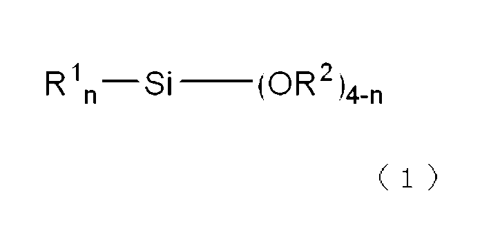
式(1)中、R1は、炭素数1~20のアルキル基又は水素原子を表す。nは1~3の整数を表す。nが2以上の場合、複数のR1は同一又は相異なってもよく、また、二つのR1は互いに結合し、アルカンジイル基を形成してもよい。R2は、炭素数1~10のアルキル基を表す。nが2以下の場合、複数のR2は同一又は相異なってもよい。
ガスバリア膜用材料は、下記式(1)で示される有機シラン化合物(有機シラン化合物(1)ともいう。)よりなる化学気相成長法用の酸化ケイ素膜用材料である。
式(1)におけるR1の炭素数1~20のアルキル基としては直鎖状、分岐鎖状、環状のいずれの構造を有してよい。また、分子内に複数のR1を有する場合、二つのR1が互いに結合しアルカンジイル基を形成したものも本発明の範囲に含まれる。炭素数1~20のアルキル基としては、高いガスバリア性が得られ、又、蒸気圧が高く気化に好適な点で、炭素数1~10のアルキル基が好ましく、更に炭素数1~5のアルキル基が更に好ましく、特に炭素数1~4のアルキル基が好ましい。また、複数のR1は、同一であっても相異なっても良い。
炭素数1~20のアルキル基におけるR1としては、メチル基、エチル基、プロピル基、イソプロピル基、ブチル基、イソブチル基、s-ブチル基、t-ブチル基、ペンチル基、1-メチルブチル基、2-メチルブチル基、3-メチルブチル基、1-エチルプロピル基、1,1-ジメチルプロピル基、1,2-ジメチルプロピル基、2,2-ジメチルプロピル基、シクロペンチル基、へキシル基、シクロヘキシル基、オクチル基、ノニル基、デシル基、イコシル基等が例示できる。
二つのR1は互いに結合しアルカンジイル基を形成してもよく、該アルカンジイル基としては、例えばプロパン-1,3-ジイル基、ブタン-1,4-ジイル基、ペンタン-1,4-ジイル基、ペンタン-1,5-ジイル基、ヘキサン-2,5-ジイル基、ヘキサン-1,6-ジイル基、ヘプタン-1,7-ジイル基等が挙げられる。
二つのR1は互いに結合しアルカンジイル基を形成してもよく、該アルカンジイル基としては、例えばプロパン-1,3-ジイル基、ブタン-1,4-ジイル基、ペンタン-1,4-ジイル基、ペンタン-1,5-ジイル基、ヘキサン-2,5-ジイル基、ヘキサン-1,6-ジイル基、ヘプタン-1,7-ジイル基等が挙げられる。
原料の入手が容易であり、式(1)で示されるガスバリア膜用材料の蒸気圧が高いという点から、R1としてはメチル基、エチル基、プロピル基、イソプロピル基、ブチル基、イソブチル基、s-ブチル基、t-ブチル基、ペンチル基、1-メチルブチル基、2-メチルブチル基、3-メチルブチル基、1-エチルプロピル基、1,1-ジメチルプロピル基、1,2-ジメチルプロピル基、2,2-ジメチルプロピル基、へキシル基、オクチル基、又はノニル基が好ましく、メチル基、エチル基、プロピル基、イソプロピル基、ブチル基、イソブチル基、s-ブチル基、t-ブチル基、ペンチル基、1-メチルブチル基、2-メチルブチル基、3-メチルブチル基、1-エチルプロピル基、1,1-ジメチルプロピル基、1,2-ジメチルプロピル基、又は2,2-ジメチルプロピル基が特に好ましい。
R2における炭素数1~10のアルキル基としては、メチル基、エチル基、プロピル基、イソプロピル基、シクロプロピル基、ブチル基、イソブチル基、s-ブチル基、t-ブチル基、ペンチル基、1-メチルブチル基、2-メチルブチル基、3-メチルブチル基、1-エチルプロピル基、1,1-ジメチルプロピル基、1,2-ジメチルプロピル基、2,2-ジメチルプロピル基等が挙げられ、その中でも原料入手が容易な点から、メチル基、エチル基、プロピル基、又はイソプロピル基が好ましく、メチル基又はエチル基が更に好ましい。
nは、1~3の整数を表す。
nは、1~3の整数を表す。
式(1)で示される有機シラン化合物の具体例としては、下記のものが挙げられる。
ジメトキシメチルシラン、トリメトキシメチルシラン、エチルジメトキシシラン、エチルトリメトキシシラン、ジメトキシプロピルシラン、トリメトキシプロピルシラン、ジメトキシイソプロピルシラン、トリメトキシイソプロピルシラン、ブチルジメトキシシラン、ブチルトリメトキシシラン、イソブチルジメトキシシラン、イソブチルトリメトキシシラン、s-ブチルジメトキシシラン、s-ブチルトリメトキシシラン、t-ブチルジメトキシシラン、t-ブチルトリメトキシシラン、ジメトキシペンチルシラン、トリメトキシペンチルシラン、1-メチルブチルジメトキシシラン、1-メチルブチルトリメトキシシラン、2-メチルブチルジメトキシシラン、2-メチルブチルトリメトキシシラン、3-メチルブチルジメトキシシラン、3-メチルブチルトリメトキシシラン、1-エチルプロピルジメトキシシラン、1-エチルプロピルトリメトキシシラン、1,1-ジメチルプロピルジメトキシシラン、1,1-ジメチルプロピルトリメトキシシラン、1,2-ジメチルプロピルジメトキシシラン、1,2-ジメチルプロピルトリメトキシシラン、2,2-ジメチルプロピルジメトキシシラン、2,2-ジメチルプロピルトリメトキシシラン、シクロペンチルジメトキシシラン、シクロペンチルトリメトキシシラン、シクロヘキシルジメトキシシラン、シクロヘキシルトリメトキシシラン、
ジメトキシメチルシラン、トリメトキシメチルシラン、エチルジメトキシシラン、エチルトリメトキシシラン、ジメトキシプロピルシラン、トリメトキシプロピルシラン、ジメトキシイソプロピルシラン、トリメトキシイソプロピルシラン、ブチルジメトキシシラン、ブチルトリメトキシシラン、イソブチルジメトキシシラン、イソブチルトリメトキシシラン、s-ブチルジメトキシシラン、s-ブチルトリメトキシシラン、t-ブチルジメトキシシラン、t-ブチルトリメトキシシラン、ジメトキシペンチルシラン、トリメトキシペンチルシラン、1-メチルブチルジメトキシシラン、1-メチルブチルトリメトキシシラン、2-メチルブチルジメトキシシラン、2-メチルブチルトリメトキシシラン、3-メチルブチルジメトキシシラン、3-メチルブチルトリメトキシシラン、1-エチルプロピルジメトキシシラン、1-エチルプロピルトリメトキシシラン、1,1-ジメチルプロピルジメトキシシラン、1,1-ジメチルプロピルトリメトキシシラン、1,2-ジメチルプロピルジメトキシシラン、1,2-ジメチルプロピルトリメトキシシラン、2,2-ジメチルプロピルジメトキシシラン、2,2-ジメチルプロピルトリメトキシシラン、シクロペンチルジメトキシシラン、シクロペンチルトリメトキシシラン、シクロヘキシルジメトキシシラン、シクロヘキシルトリメトキシシラン、
ジエトキシシラン、トリメトキシシラン、ジエトキシメチルシラン、トリエトキシメチルシラン、ジエトキシエチルシラン、トリエトキシエチルシラン、ジエトキシプロピルシラン、トリエトキシプロピルシラン、ジエトキシイソプロピルシラン、トリエトキシイソプロピルシラン、ブチルジエトキシシラン、ブチルトリエトキシシラン、イソブチルジエトキシシラン、イソブチルトリエトキシシラン、s-ブチルジエトキシシラン、s-ブチルトリエトキシシラン、t-ブチルジエトキシシラン、t-ブチルトリエトキシシラン、ジエトキシペンチルシラン、トリエトキシペンチルシラン、1-メチルブチルジエトキシシラン、1-メチルブチルトリエトキシシラン、2-メチルブチルジエトキシシラン、2-メチルブチルトリエトキシシラン、3-メチルブチルジエトキシシラン、3-メチルブチルトリエトキシシラン、1-エチルプロピルジエトキシシラン、1-エチルプロピルトリエトキシシラン、1,1-ジメチルプロピルジエトキシシラン、1,1-ジメチルプロピルトリエトキシシラン、1,2-ジメチルプロピルジエトキシシラン、1,2-ジメチルプロピルトリエトキシシラン、2,2-ジメチルプロピルジエトキシシラン、2,2-ジメチルプロピルトリエトキシシラン、シクロペンチルジエトキシシラン、シクロペンチルトリエトキシシラン、シクロヘキシルジエトキシシラン、シクロヘキシルトリエトキシシラン、
トリプロポキシシラン、メチルトリプロポキシシラン、エチルトリプロポキシシラン、トリプロポキシプロピルシラン、トリプロポキシイソプロピルシラン、ブチルトリプロポキシシラン、イソブチルトリプロポキシシラン、s-ブチルトリプロポキシシラン、t-ブチルトリプロポキシシラン、ペンチルトリイソプロポキシシラン、1-メチルブチルトリイソプロポキシシラン、2-メチルブチルトリイソプロポキシシラン、3-メチルブチルトリイソプロポキシシラン、1-エチルプロピルトリイソプロポキシシラン、1,1-ジメチルプロピルトリイソプロポキシシラン、1,2-ジメチルプロピルトリイソプロポキシシラン、2,2-ジメチルプロピルトリイソプロポキシシラン、シクロペンチルトリイソプロポキシシラン、
メトキシジメチルシラン、ジメトキシジメチルシラン、エトキシジメチルシラン、ジエトキシジメチルシラン、ジメチルプロポキシシラン、ジメチルジプロポキシシラン、ジメチルイソプロポキシシラン、ジメチルジイソプロポキシシラン、ジエチルメトキシシラン、ジエチルジメトキシシラン、エトキシジエチルシラン、ジエトキシジエチルシラン、ジエチルプロポキシシラン、ジエチルジプロポキシシラン、ジエチルイソプロポキシシラン、ジエチルジイソプロポキシシラン、ジイソプロピルメトキシシラン、ジイソプロピルジメトシキシラン、ジイソプロピルエトシキシラン、ジイソプロピルジエトシキシラン、ジイソプロピルプロポキシシラン、ジイソプロピルジプロポキシシラン、ジイソプロピルイソプロポキシシラン、ジイソプロピルジイソプロポキシシラン、ジ-s-ブチルメトシキシラン、ジ-s-ブチルジメトシキシラン、ジ-s-ブチルエトシキシラン、ジ-s-ブチルジエトシキシラン、ジ-s-ブチルプロポキシシラン、ジ-s-ブチルジプロポキシシラン、ジ-s-ブチルイソプロポキシシラン、ジ-s-ブチルジイソプロポキシシラン、ジ-t-ブチルメトシキシラン、ジ-t-ブチルジメトシキシラン、ジ-t-ブチルエトシキシラン、ジ-t-ブチルジエトシキシラン、ジ-t-ブチルプロポキシシラン、ジ-t-ブチルジプロポキシシラン、ジ-t-ブチルイソプロポキシシラン、ジ-t-ブチルジイソプロポキシシラン、メトキシトリメチルシラン、エトキシトリメチルシラン、トリエチルメトキシシラン、エトキシトリエチルシラン、1,1-ジメトキシ-1-シラシクロペンタン、1,1-ジエトキシ-1-シラシクロペンタン、1,1-ジメトキシ-1-シラシクロペンタン等。
式(1)で示される有機シラン化合物は、上記の中でも、蒸気圧が高く、又はWVTRが低いガスバリア膜用材料となることから、下記のものが好ましい。
ジメトキシメチルシラン、トリメトキシメチルシラン、エチルジメトキシシラン、エチルトリメトキシシラン、ジメトキシプロピルシラン、トリメトキシプロピルシラン、ジメトキシイソプロピルシラン、トリメトキシイソプロピルシラン、ブチルジメトキシシラン、ブチルトリメトキシシラン、イソブチルジメトキシシラン、イソブチルトリメトキシシラン、s-ブチルジメトキシシラン、s-ブチルトリメトキシシラン、t-ブチルジメトキシシラン、t-ブチルトリメトキシシラン、1-メチルブチルジメトキシシラン、1-メチルブチルトリメトキシシラン、2-メチルブチルジメトキシシラン、2-メチルブチルトリメトキシシラン、3-メチルブチルジメトキシシラン、3-メチルブチルトリメトキシシラン、1,1-ジメチルプロピルジメトキシシラン、1,1-ジメチルプロピルトリメトキシシラン、1,2-ジメチルプロピルジメトキシシラン、1,2-ジメチルプロピルトリメトキシシラン、2,2-ジメチルプロピルジメトキシシラン、2,2-ジメチルプロピルトリメトキシシラン、トリメトキシシクロペンチルシラン、
ジエトキシメチルシラン、トリエトキシメチルシラン、エチルジエトキシシラン、エチルトリエトキシシラン、ジエトキシプロピルシラン、トリエトキシプロピルシラン、ジエトキシイソプロピルシラン、トリエトキシイソプロピルシラン、ブチルジエトキシシラン、ブチルトリエトキシシラン、イソブチルジエトキシシラン、イソブチルトリエトキシシラン、s-ブチルジエトキシシラン、s-ブチルトリエトキシシラン、t-ブチルジエトキシシラン、t-ブチルトリエトキシシラン、1-メチルブチルジエトキシシラン、1-メチルブチルトリエトキシシラン、2-メチルブチルジエトキシシラン、2-メチルブチルトリエトキシシラン、3-メチルブチルジエトキシシラン、3-メチルブチルトリエトキシシラン、1,1-ジメチルプロピルジエトキシシラン、1,1-ジメチルプロピルトリエトキシシラン、1,2-ジメチルプロピルジエトキシシラン、1,2-ジメチルプロピルトリエトキシシラン、2,2-ジメチルプロピルジエトキシシラン、2,2-ジメチルプロピルトリエトキシシラン、トリエトキシシクロペンチルシラン、
ジメトキシメチルシラン、トリメトキシメチルシラン、エチルジメトキシシラン、エチルトリメトキシシラン、ジメトキシプロピルシラン、トリメトキシプロピルシラン、ジメトキシイソプロピルシラン、トリメトキシイソプロピルシラン、ブチルジメトキシシラン、ブチルトリメトキシシラン、イソブチルジメトキシシラン、イソブチルトリメトキシシラン、s-ブチルジメトキシシラン、s-ブチルトリメトキシシラン、t-ブチルジメトキシシラン、t-ブチルトリメトキシシラン、1-メチルブチルジメトキシシラン、1-メチルブチルトリメトキシシラン、2-メチルブチルジメトキシシラン、2-メチルブチルトリメトキシシラン、3-メチルブチルジメトキシシラン、3-メチルブチルトリメトキシシラン、1,1-ジメチルプロピルジメトキシシラン、1,1-ジメチルプロピルトリメトキシシラン、1,2-ジメチルプロピルジメトキシシラン、1,2-ジメチルプロピルトリメトキシシラン、2,2-ジメチルプロピルジメトキシシラン、2,2-ジメチルプロピルトリメトキシシラン、トリメトキシシクロペンチルシラン、
ジエトキシメチルシラン、トリエトキシメチルシラン、エチルジエトキシシラン、エチルトリエトキシシラン、ジエトキシプロピルシラン、トリエトキシプロピルシラン、ジエトキシイソプロピルシラン、トリエトキシイソプロピルシラン、ブチルジエトキシシラン、ブチルトリエトキシシラン、イソブチルジエトキシシラン、イソブチルトリエトキシシラン、s-ブチルジエトキシシラン、s-ブチルトリエトキシシラン、t-ブチルジエトキシシラン、t-ブチルトリエトキシシラン、1-メチルブチルジエトキシシラン、1-メチルブチルトリエトキシシラン、2-メチルブチルジエトキシシラン、2-メチルブチルトリエトキシシラン、3-メチルブチルジエトキシシラン、3-メチルブチルトリエトキシシラン、1,1-ジメチルプロピルジエトキシシラン、1,1-ジメチルプロピルトリエトキシシラン、1,2-ジメチルプロピルジエトキシシラン、1,2-ジメチルプロピルトリエトキシシラン、2,2-ジメチルプロピルジエトキシシラン、2,2-ジメチルプロピルトリエトキシシラン、トリエトキシシクロペンチルシラン、
ジメトキシメチルシラン、ジメトキシジメチルシラン、ジエトキシジメチルシラン、ジエチルジメトキシシラン、ジエトキシジエチルシラン、ジエチルジプロポキシシラン、ジイソプロピルジメトシキシラン、ジイソプロピルジエトシキシラン、ジ-s-ブチルジメトシキシラン、ジ-s-ブチルジエトシキシラン、ジ-t-ブチルジメトシキシラン、又はジ-t-ブチルジエトシキシランが好ましく、
ジメトキシメチルシラン、トリメトキシメチルシラン、エチルトリメトキシシラン、トリメトキシプロピルシラン、イソプロピルトリメトキシシラン、ブチルトリメトキシシラン、イソブチルトリメトキシシラン、s-ブチルトリメトキシシラン、t-ブチルジメトキシシラン、t-ブチルトリメトキシシラン、1-メチルブチルトリメトキシシラン、1,1-ジメチルプロピルトリメトキシシラン、1,2-ジメチルプロピルトリメトキシシラン、
ジメトキシメチルシラン、トリメトキシメチルシラン、エチルトリメトキシシラン、トリメトキシプロピルシラン、イソプロピルトリメトキシシラン、ブチルトリメトキシシラン、イソブチルトリメトキシシラン、s-ブチルトリメトキシシラン、t-ブチルジメトキシシラン、t-ブチルトリメトキシシラン、1-メチルブチルトリメトキシシラン、1,1-ジメチルプロピルトリメトキシシラン、1,2-ジメチルプロピルトリメトキシシラン、
ジエトキシメチルシラン、トリエトキシメチルシラン、エチルトリエトキシシラン、トリエトキシプロピルシラン、トリエトキシイソプロピルシラン、ブチルトリエトキシシラン、イソブチルトリエトキシシラン、s-ブチルトリエトキシシラン、t-ブチルジエトキシシラン、t-ブチルトリエトキシシラン、1-メチルブチルトリエトキシシラン、1,1-ジメチルプロピルトリエトキシシラン、1,2-ジメチルプロピルトリエトキシシラン、ジメトキシメチルシラン、ジメトキシジメチルシラン、ジエトキシジメチルシラン、ジエチルジメトキシシラン、又はジエトキシジエチルシラン。
式(1)で示されるガスバリア膜用材料である有機シラン化合物の入手方法について説明する。
式(1)で示される有機シラン化合物は、市販品そのままでも、又はそれを適宜精製して用いても、あるいは適宜合成したものを用いても良い。これらの有機シラン化合物は、アルキルハロシラン化合物にアルコール及び/又は金属アルコキシドを作用させる方法(合成法1.例えば、K. Lin、R. J. Wiles、C. B. Kelly、G. H. M.Davies、G. A. Molander、ACS Catalysis、2017年、7巻、5129~5133頁.に記載の方法)、又は、アルコキシシラン類にアルキルアルキルマグネシウムハライド又はアルキルリチウムを作用させる方法(合成法2.例えば、S. Masaoka、T. Banno、M. Ishikawa、Journal of Organometallic Chemistry、2006年、691巻、182~192頁.に記載の方法)等により合成することができる。合成により得た有機シラン化合物は、再結晶、蒸留、及びカラムクロマトグラフィー等の汎用的な方法により精製して成膜に用いることもできる。
式(1)で示される有機シラン化合物は、市販品そのままでも、又はそれを適宜精製して用いても、あるいは適宜合成したものを用いても良い。これらの有機シラン化合物は、アルキルハロシラン化合物にアルコール及び/又は金属アルコキシドを作用させる方法(合成法1.例えば、K. Lin、R. J. Wiles、C. B. Kelly、G. H. M.Davies、G. A. Molander、ACS Catalysis、2017年、7巻、5129~5133頁.に記載の方法)、又は、アルコキシシラン類にアルキルアルキルマグネシウムハライド又はアルキルリチウムを作用させる方法(合成法2.例えば、S. Masaoka、T. Banno、M. Ishikawa、Journal of Organometallic Chemistry、2006年、691巻、182~192頁.に記載の方法)等により合成することができる。合成により得た有機シラン化合物は、再結晶、蒸留、及びカラムクロマトグラフィー等の汎用的な方法により精製して成膜に用いることもできる。


<酸化ケイ素膜の製造方法>
本発明の酸化ケイ素膜は、上記ガスバリア膜用材料を、成膜圧力(ゲージ圧、特に、言及のない限り同じである。)0.01Pa以上20Pa未満の条件でプラズマ励起化学気相成長法により成膜することにより製造する。
なお、酸化ケイ素膜の製造方法では、以下の通り基板上に酸化ケイ素膜を製造することから、同時に積層膜も製造することができる。
本発明の酸化ケイ素膜は、上記ガスバリア膜用材料を、成膜圧力(ゲージ圧、特に、言及のない限り同じである。)0.01Pa以上20Pa未満の条件でプラズマ励起化学気相成長法により成膜することにより製造する。
なお、酸化ケイ素膜の製造方法では、以下の通り基板上に酸化ケイ素膜を製造することから、同時に積層膜も製造することができる。
酸化ケイ素膜を製造する際には、プラズマ励起化学気相成長法(PECVD法)で成膜し、その際に有機シラン化合物(1)に加え酸素を供給することが必須である。具体的には、PECVD法で有機シラン化合物(1)及び酸素を原料としてガスバリア膜を製造する際、有機シラン化合物(1)を気化して成膜用基板を設置した成膜室に供給する。気化する方法としては、例えば加熱した恒温槽に有機シラン化合物(1)を入れ、真空ポンプ等を用いて減圧して気化する方法、加熱した恒温槽に有機シラン化合物(1)を入れ、ヘリウム、ネオン、アルゴン、クリプトン、キセノンもしくは窒素などのキャリアガスを吹き込み気化する方法、又は有機シラン化合物(1)をそのままもしくは溶液とし、これを気化器に送って加熱して気化器内で気化する方法(リキッドインジェクション法)等がある。
溶液とする場合に用いる溶媒としては、1,2-ジメトキシエタン、ジグリム、トリグリム、ジオキサン、テトラヒドロフラン、シクロペンチルメチルエーテル等のエーテル類、ヘキサン、シクロヘキサン、メチルシクロヘキサン、エチルシクロヘキサン、ヘプタン、オクタン、ノナン、デカン、ベンゼン、トルエン、エチルベンゼン、キシレン等の炭化水素類を例示することが出来る。これらのうち一種を単独で用いても、二種以上を任意の比で混合して用いることが出来る。
溶液とする場合に用いる溶媒としては、1,2-ジメトキシエタン、ジグリム、トリグリム、ジオキサン、テトラヒドロフラン、シクロペンチルメチルエーテル等のエーテル類、ヘキサン、シクロヘキサン、メチルシクロヘキサン、エチルシクロヘキサン、ヘプタン、オクタン、ノナン、デカン、ベンゼン、トルエン、エチルベンゼン、キシレン等の炭化水素類を例示することが出来る。これらのうち一種を単独で用いても、二種以上を任意の比で混合して用いることが出来る。
このようにして成膜室に供給した有機シラン化合物(1)及び酸素は、成膜室内で発生させたプラズマにより反応し、成膜用基板上へガスバリア膜が形成される。成膜はプラズマのみでも進行するが、光照射や成膜用基板の加熱等を併用してもよい。
プラズマの発生源には特に限定はなく、容量結合プラズマ、誘導結合プラズマ、ヘリコン波プラズマ、表面波プラズマ、電子サイクロトロン共鳴プラズマ等が挙げられる。
プラズマの発生源には特に限定はなく、容量結合プラズマ、誘導結合プラズマ、ヘリコン波プラズマ、表面波プラズマ、電子サイクロトロン共鳴プラズマ等が挙げられる。
酸化ケイ素膜の製造に用いる成膜装置としては、当業者が通常用いる化学気相蒸着用装置を用いればよく、例えばバッチ式、枚葉式、ロールツーロール方式等が挙げられる。
成膜室の圧力は0.01Pa以上20Pa未満の範囲にあることが必須であり、得られるガスバリア膜のWVTRが低い点及び真空度の制御が容易な点から0.1Pa以上15Pa未満が好ましい。
高周波電源(RF電源)の電力は100W以上であることが好ましく、得られるガスバリア膜のWVTRが低い点から200W~1500Wが更に好ましい。
プラズマ放電のために電極に印可する電力の密度は、0.1W/cm2以上あることが好ましく、得られるガスバリア膜のWVTRが低い点から2.0W/cm2~100W/cm2が更に好ましい。
成膜中の成膜用基板の温度は特に限定はなく、成膜用基板の耐熱温度以下であり、0℃~300℃の範囲であることが好ましい。
成膜室の圧力は0.01Pa以上20Pa未満の範囲にあることが必須であり、得られるガスバリア膜のWVTRが低い点及び真空度の制御が容易な点から0.1Pa以上15Pa未満が好ましい。
高周波電源(RF電源)の電力は100W以上であることが好ましく、得られるガスバリア膜のWVTRが低い点から200W~1500Wが更に好ましい。
プラズマ放電のために電極に印可する電力の密度は、0.1W/cm2以上あることが好ましく、得られるガスバリア膜のWVTRが低い点から2.0W/cm2~100W/cm2が更に好ましい。
成膜中の成膜用基板の温度は特に限定はなく、成膜用基板の耐熱温度以下であり、0℃~300℃の範囲であることが好ましい。
成膜用基板の種類は特に限定はなく、例えばポリエチレンテレフタレート(PET)、ポリエチレンナフタレート(PEN)、ポリカーボネート(PC)、ポリアミド(PA)、ポリイミド(PI)、シクロオレフィンポリマー(COP)、ポリエチレン(PE)、ポリプロピレン(PP)、ポリスチレン(PS)、ポリ塩化ビニル(PVC)、ポリビニルアルコール(PVA)、トリアセチルセルロース(TAC)、ポリエーテルスルホン(PES)、シクロオレフィン共重合体(COC)、ポリアクリロニトリル(PAN)、エチレン-ビニルアルコール共重合体(EVOH)、ABS樹脂、メタクリル樹脂、エポキシ樹脂、変性ポリフェニレンエーテル、ポリアセタール、ポリブチレンテレフタレート、ポリアクリレート、ポリアリレート、ポリスルホン、ポリアミドイミド、ポリエーテルイミド、ポリフェニレンスルフィド、ポリエーテルエーテルケトン、フッ素樹脂等が挙げられる。
成膜時に供給する有機シラン化合物(1)の供給流量をX、酸素の供給流量をYとすると、有機シラン化合物(1)に対する酸素の比(Y/X)は1以上が好ましく、5~100が更に好ましい。
以下、実施例により本発明をさらに詳細に説明するが、本発明はこれらに限定されるものではない。
容量結合型PECVD法により成膜を行う一般的なCVD装置を用いて、基板にガスバリア膜を成膜した。成膜用基板には厚さ125μmのポリエチレンナフタレート(PEN)フィルム(可視光線透過率88.3%、表面粗さRa0.71nm)、厚さ125μmのポリエチレンテレフタレート(PET)フィルム(可視光線透過率89.3%、表面粗さRa1.17nm)を使用した。原料ガスとして、恒温槽中で気化させた有機シラン化合物、酸素ガス、アルゴンガスを用いた。さらに、電源として周波数13.56MHzの高周波電源を用いた。
容量結合型PECVD法により成膜を行う一般的なCVD装置を用いて、基板にガスバリア膜を成膜した。成膜用基板には厚さ125μmのポリエチレンナフタレート(PEN)フィルム(可視光線透過率88.3%、表面粗さRa0.71nm)、厚さ125μmのポリエチレンテレフタレート(PET)フィルム(可視光線透過率89.3%、表面粗さRa1.17nm)を使用した。原料ガスとして、恒温槽中で気化させた有機シラン化合物、酸素ガス、アルゴンガスを用いた。さらに、電源として周波数13.56MHzの高周波電源を用いた。
成膜した膜の膜厚みは、電界放射型走査電子顕微鏡(日本電子社製、FE-SEM)JSM-7600Fを用いて膜の断面像を撮影し、概算した。
ガスバリア性能の指標となる水蒸気透過率(WVTR)は、水分透過率測定装置(GTRテック社製、GTR3000シリーズ)を用いてガスクロマトグラフ法(GC法)で測定した。
ガスバリア膜の膜組成(炭素濃度を含む)はX線光電子分光分析装置(アルバック・ファイ社製、XPS)PHI5000 VersaProbeIIを用いて分析した。
ガスバリア性能の指標となる水蒸気透過率(WVTR)は、水分透過率測定装置(GTRテック社製、GTR3000シリーズ)を用いてガスクロマトグラフ法(GC法)で測定した。
ガスバリア膜の膜組成(炭素濃度を含む)はX線光電子分光分析装置(アルバック・ファイ社製、XPS)PHI5000 VersaProbeIIを用いて分析した。
合成した有機シラン化合物(1)の分析は、1H-NMR(プロトン核磁気共鳴スペクトル)、13C-NMR(炭素13核磁気共鳴スペクトル)及び29Si-NMR(ケイ素29核磁気共鳴スペクトル)測定はBruker-Avance社のDPX-400核磁気共鳴分光計を用い、溶媒には重クロロホルムを用いた。IR(赤外吸収)スペクトルは、堀場製作所社のFT-720分光光度計を用い、SensIRtechnologies社のDuraSamplIRII(反射型)を用いて測定を行った。質量スペクトル測定は、ガスクロマトグラフィー型質量分析装置(島津製作所社製、GCMS-QP2010型)を使用し、キャピラリーカラムにはアジレント・テクノロジー社製のDB-5MSを使用した。
(実施例1)t-ブチルトリエトキシシランを用いた成膜
K. Lin、R. J. Wiles、C. B. Kelly、G. H. M.Davies、G. A. Molander、ACS Catalysis、2017年、7巻、5129~5133頁.に記載の方法を参考に合成したt-ブチルトリエトキシシランを用い、酸素と共にPECVD法によりPENフィルム上に酸化ケイ素膜を成膜した。t-ブチルトリエトキシシランの供給流量を80sccm、酸素供給流量を2100sccm、成膜室圧力を8Pa、電源周波数13.56MHzの高周波電源(RF電源)の電力を1000Wとし、14分間成膜を行った。また、t-ブチルトリエトキシシランの供給流量に対する酸素の供給流量比(Y/X)は26.3であった。
K. Lin、R. J. Wiles、C. B. Kelly、G. H. M.Davies、G. A. Molander、ACS Catalysis、2017年、7巻、5129~5133頁.に記載の方法を参考に合成したt-ブチルトリエトキシシランを用い、酸素と共にPECVD法によりPENフィルム上に酸化ケイ素膜を成膜した。t-ブチルトリエトキシシランの供給流量を80sccm、酸素供給流量を2100sccm、成膜室圧力を8Pa、電源周波数13.56MHzの高周波電源(RF電源)の電力を1000Wとし、14分間成膜を行った。また、t-ブチルトリエトキシシランの供給流量に対する酸素の供給流量比(Y/X)は26.3であった。
得られた酸化ケイ素膜の厚みは800nmであった。膜の組成は、Si=33atom%、O=67atom%であり、炭素濃度は1.0atm%未満であった。WVTRは2.0×10⁻⁴g/m2・dayであった。
酸化ケイ素膜とPENフィルムからなる積層膜の可視光線透過率は88.2%であった。表面粗さ(Ra)は0.68nmであった。
t-ブチルトリエトキシシランを用い、酸素と共にPECVD法によりPENフィルム上に酸化ケイ素膜を成膜した。t-ブチルトリエトキシシランの供給流量を80sccm、酸素供給流量を2100sccm、成膜室圧力を8Pa、電源周波数13.56MHzの高周波電源(RF電源)の電力を1000Wとし、7分間成膜を行った。また、t-ブチルトリエトキシシランの供給流量に対する酸素の供給流量比(Y/X)は26.3であった。
酸化ケイ素膜とPENフィルムからなる積層膜の可視光線透過率は88.2%であった。表面粗さ(Ra)は0.68nmであった。
t-ブチルトリエトキシシランを用い、酸素と共にPECVD法によりPENフィルム上に酸化ケイ素膜を成膜した。t-ブチルトリエトキシシランの供給流量を80sccm、酸素供給流量を2100sccm、成膜室圧力を8Pa、電源周波数13.56MHzの高周波電源(RF電源)の電力を1000Wとし、7分間成膜を行った。また、t-ブチルトリエトキシシランの供給流量に対する酸素の供給流量比(Y/X)は26.3であった。
得られた酸化ケイ素膜の厚みは400nmであった。WVTRは4.3×10⁻⁴g/m2・dayであった。酸化ケイ素膜とPENフィルムからなる積層膜の可視光線透過率は88.5%であった。
t-ブチルトリエトキシシランを用い、酸素と共にPECVD法により成膜すると、酸化ケイ素膜厚が400nmと薄い膜であっても、WVTRが10-3g/m2・dayオーダー以下の10-4g/m2・dayオーダーを示し、ガスバリア膜として好適である。
t-ブチルトリエトキシシランを用い、酸素と共にPECVD法により成膜すると、酸化ケイ素膜厚が400nmと薄い膜であっても、WVTRが10-3g/m2・dayオーダー以下の10-4g/m2・dayオーダーを示し、ガスバリア膜として好適である。
(実施例2)t-ブチルトリエトキシシランを用いた成膜
実施例1と同様に得たt-ブチルトリエトキシシランを用い、酸素と共にPECVD法によりPETフィルム上に酸化ケイ素膜を成膜した。t-ブチルトリエトキシシランの供給流量を80sccm、酸素供給流量を2100sccm、成膜室圧力を8Pa、電源周波数13.56MHzの高周波電源(RF電源)の電力を1000Wとし、8分間成膜を行った。また、t-ブチルトリエトキシシランの供給流量に対する酸素の供給流量比(Y/X)は26.3であった。
実施例1と同様に得たt-ブチルトリエトキシシランを用い、酸素と共にPECVD法によりPETフィルム上に酸化ケイ素膜を成膜した。t-ブチルトリエトキシシランの供給流量を80sccm、酸素供給流量を2100sccm、成膜室圧力を8Pa、電源周波数13.56MHzの高周波電源(RF電源)の電力を1000Wとし、8分間成膜を行った。また、t-ブチルトリエトキシシランの供給流量に対する酸素の供給流量比(Y/X)は26.3であった。
得られた酸化ケイ素膜の厚みは500nmであった。WVTRは3.9×10⁻³g/m2・dayであった。酸化ケイ素膜とPETフィルムからなる積層膜の可視光線透過率は91.0%であった。
t-ブチルトリエトキシシランを用い、酸素と共にPECVD法により成膜すると、酸化ケイ素膜厚が500nmと薄い膜であってもWVTRが10-3g/m2・dayオーダーを示し、ガスバリア膜として好適である。
t-ブチルトリエトキシシランを用い、酸素と共にPECVD法により成膜すると、酸化ケイ素膜厚が500nmと薄い膜であってもWVTRが10-3g/m2・dayオーダーを示し、ガスバリア膜として好適である。
(実施例3)イソプロピルトリメトキシシランを用いた成膜
K. Lin、R. J. Wiles、C. B. Kelly、G. H. M.Davies、G. A. Molander、ACS Catalysis、2017年、7巻、5129~5133頁.に記載の方法を参考に合成したイソプロピルトリメトキシシランを用い、酸素と共にPECVD法によりPENフィルム上に酸化ケイ素膜を成膜した。イソプロピルトリメトキシシランの供給流量を80sccm、酸素供給流量を2100sccm、成膜室圧力を8Pa、電源周波数13.56MHzの高周波電源(RF電源)の電力を1000Wとし、11分間成膜を行った。また、イソプロピルトリメトキシシランの供給流量に対する酸素の供給流量比(Y/X)は26.3であった。
K. Lin、R. J. Wiles、C. B. Kelly、G. H. M.Davies、G. A. Molander、ACS Catalysis、2017年、7巻、5129~5133頁.に記載の方法を参考に合成したイソプロピルトリメトキシシランを用い、酸素と共にPECVD法によりPENフィルム上に酸化ケイ素膜を成膜した。イソプロピルトリメトキシシランの供給流量を80sccm、酸素供給流量を2100sccm、成膜室圧力を8Pa、電源周波数13.56MHzの高周波電源(RF電源)の電力を1000Wとし、11分間成膜を行った。また、イソプロピルトリメトキシシランの供給流量に対する酸素の供給流量比(Y/X)は26.3であった。
得られた酸化ケイ素膜の厚みは800nmであった。膜の組成は、Si=33atom%、O=67atom%であり、炭素濃度は1.0atm%未満であった。WVTRは2.0×10⁻⁴g/m2・dayであった。
酸化ケイ素膜とPENフィルムからなる積層膜の可視光線透過率は88.2%であった。表面粗さ表面粗さ(Ra)は0.67nmであった。
イソプロピルトリメトキシシランを用い、酸素と共にPECVD法によりPENフィルム上に酸化ケイ素膜を成膜した。イソプロピルトリメトキシシランの供給流量を80sccm、酸素供給流量を2100sccm、成膜室圧力を8Pa、電源周波数13.56MHzの高周波電源(RF電源)の電力を1000Wとし3分間成膜を行った。また、イソプロピルトリメトキシシランの供給流量に対する酸素の供給流量比(Y/X)は26.3であった。
酸化ケイ素膜とPENフィルムからなる積層膜の可視光線透過率は88.2%であった。表面粗さ表面粗さ(Ra)は0.67nmであった。
イソプロピルトリメトキシシランを用い、酸素と共にPECVD法によりPENフィルム上に酸化ケイ素膜を成膜した。イソプロピルトリメトキシシランの供給流量を80sccm、酸素供給流量を2100sccm、成膜室圧力を8Pa、電源周波数13.56MHzの高周波電源(RF電源)の電力を1000Wとし3分間成膜を行った。また、イソプロピルトリメトキシシランの供給流量に対する酸素の供給流量比(Y/X)は26.3であった。
得られた酸化ケイ素膜の厚みは200nmであった。WVTRは6.9×10⁻⁴g/m2・dayであった。酸化ケイ素膜とPENフィルムからなる積層膜の可視光線透過率は88.4%であった。
イソプロピルトリメトキシシランを用い、酸素と共にPECVD法により成膜すると、酸化ケイ素膜の厚みが200nmと薄い膜であってもWVTRが10-3g/m2・dayオーダー以下の10-4g/m2・dayオーダーを示し、ガスバリア膜として好適である。
イソプロピルトリメトキシシランを用い、酸素と共にPECVD法により成膜すると、酸化ケイ素膜の厚みが200nmと薄い膜であってもWVTRが10-3g/m2・dayオーダー以下の10-4g/m2・dayオーダーを示し、ガスバリア膜として好適である。
(合成例1)(1,2-ジメチルプロピル)トリメトキシシランの合成
磁気撹拌子、ジムロート冷却管、滴下ロート及び三方コックを備えた500mL三口フラスコをアルゴンで置換し、脱水メタノール136g(4.26mol)、トリエチルアミン422g(4.17mol)及びジエチルエーテル1800mLを収めた。反応容器を氷浴で冷やしながら、滴下ロートから文献記載法(M.G.Voronkov,N.G.Romanova,L.G.Smirnova,Chemicke Listy pro Vedu a Prumysl,52巻,640~653頁,1958年)に従って合成したトリクロロ-1,2-ジメチルプロピルシラン275g(1.34mol)を3.5時間かけて滴下し、さらに16時間室温で撹拌した。反応混合物をブフナー漏斗でろ過し、固体不純物をろ別した。ろ液をロータリーエバポレーターで濃縮し、ヘキサンを加え水で3回洗浄した。有機層を無水硫酸マグネシウムで乾燥後にろ過し、再度ロータリーエバポレーターで濃縮した。得られた混合物を減圧蒸留(沸点79℃/3.3kPa)することにより、(1,2-ジメチルプロピル)トリメトキシシランを無色透明な液体として226g(収率87.7%)得た。
磁気撹拌子、ジムロート冷却管、滴下ロート及び三方コックを備えた500mL三口フラスコをアルゴンで置換し、脱水メタノール136g(4.26mol)、トリエチルアミン422g(4.17mol)及びジエチルエーテル1800mLを収めた。反応容器を氷浴で冷やしながら、滴下ロートから文献記載法(M.G.Voronkov,N.G.Romanova,L.G.Smirnova,Chemicke Listy pro Vedu a Prumysl,52巻,640~653頁,1958年)に従って合成したトリクロロ-1,2-ジメチルプロピルシラン275g(1.34mol)を3.5時間かけて滴下し、さらに16時間室温で撹拌した。反応混合物をブフナー漏斗でろ過し、固体不純物をろ別した。ろ液をロータリーエバポレーターで濃縮し、ヘキサンを加え水で3回洗浄した。有機層を無水硫酸マグネシウムで乾燥後にろ過し、再度ロータリーエバポレーターで濃縮した。得られた混合物を減圧蒸留(沸点79℃/3.3kPa)することにより、(1,2-ジメチルプロピル)トリメトキシシランを無色透明な液体として226g(収率87.7%)得た。
質量スペクトル(EI,70eV)m/z(%)177([M-CH3]+,1.1),121(Si(OMe)3
+,100).1H-NMR(400MHz,CDCl3)δ(ppm)0.83~0.90(m,1H),0.92~1.00(m,9H),1.78~1.90(m,1H),3.58(s,9H).13C-NMR(100MHz,CDCl3)δ(ppm)10.01,20.57,22.09,23.53,28.76,50.65.29Si-NMR(80MHz,CDCl3)δ(ppm)-43.7.IR(薄膜,cm-1)2956,2945,2875,2841,1466,1387,1375,1365,1230,1190,1082,910,793,727。
(実施例4)(1,2-ジメチルプロピル)トリメトキシシランを用いた成膜
合成例1で得られた(1,2-ジメチルプロピル)トリメトキシシランを用い、酸素と共にPECVD法によりPENフィルム上に酸化ケイ素膜を成膜した。(1,2-ジメチルプロピル)トリメトキシシランの供給流量を80sccm、酸素供給流量を2100sccm、成膜室の圧力を8Pa、電源周波数13.56MHzの高周波電源(RF電源)の電力を1000Wとし、11分間成膜を行った。また、(1,2-ジメチルプロピル)トリメトキシシランの流量に対する酸素の流量比(Y/X)は26.3であった。
得られた酸化ケイ素膜の厚みは800nmであった。膜の組成は、Si=33atom%、O=67atom%であり、炭素濃度は1.0atm%未満であった。WVTRは2.0×10⁻⁴g/m2・dayであった。
酸化ケイ素膜とPENフィルムからなる積層膜の可視光線透過率は88.1%であった。表面粗さ(Ra)は0.62nmであった。
合成例1で得られた(1,2-ジメチルプロピル)トリメトキシシランを用い、酸素と共にPECVD法によりPENフィルム上に酸化ケイ素膜を成膜した。(1,2-ジメチルプロピル)トリメトキシシランの供給流量を80sccm、酸素供給流量を2100sccm、成膜室の圧力を8Pa、電源周波数13.56MHzの高周波電源(RF電源)の電力を1000Wとし、11分間成膜を行った。また、(1,2-ジメチルプロピル)トリメトキシシランの流量に対する酸素の流量比(Y/X)は26.3であった。
得られた酸化ケイ素膜の厚みは800nmであった。膜の組成は、Si=33atom%、O=67atom%であり、炭素濃度は1.0atm%未満であった。WVTRは2.0×10⁻⁴g/m2・dayであった。
酸化ケイ素膜とPENフィルムからなる積層膜の可視光線透過率は88.1%であった。表面粗さ(Ra)は0.62nmであった。
合成例1で得られた(1,2-ジメチルプロピル)トリメトキシシランを用い、酸素と共にPECVD法によりPENフィルム上に酸化ケイ素膜を成膜した。(1,2-ジメチルプロピル)トリメトキシシランの供給流量を80sccm、酸素供給流量を2100sccm、成膜室の圧力を8Pa、電源周波数13.56MHzの高周波電源(RF電源)の電力を1000Wとし、3分間成膜を行った。また、(1,2-ジメチルプロピル)トリメトキシシランの流量に対する酸素の流量比(Y/X)は26.3であった。
得られた酸化ケイ素膜の厚みは250nmであった。WVTRは7.2×10⁻⁴g/m2・dayであった。酸化ケイ素膜とPENフィルムからなる積層膜の可視光線透過率は88.2%であった。
(1,2-ジメチルプロピル)トリメトキシシランを用い、酸素と共にPECVD法により成膜すると、酸化ケイ素膜厚が250nmと薄い膜であってもWVTRが10-3g/m2・dayオーダー以下の10-4g/m2・dayオーダーを示し、ガスバリア膜として好適である。
(1,2-ジメチルプロピル)トリメトキシシランを用い、酸素と共にPECVD法により成膜すると、酸化ケイ素膜厚が250nmと薄い膜であってもWVTRが10-3g/m2・dayオーダー以下の10-4g/m2・dayオーダーを示し、ガスバリア膜として好適である。
(実施例5)t-ブチルトリメトキシシランを用いた成膜
K. Lin、R. J. Wiles、C. B. Kelly、G. H. M.Davies、G. A. Molander、ACS Catalysis、2017年、7巻、5129~5133頁.に記載の方法を参考に合成したt-ブチルトリメトキシシランを用い、酸素と共にPECVD法によりPENフィルム上に酸化ケイ素膜を成膜した。t-ブチルトリメトキシシランの供給流量を80sccm、酸素供給流量を2100sccm、成膜室の圧力を8Pa、電源周波数13.56MHzの高周波電源(RF電源)の電力を1000Wとし、14分間成膜を行った。また、t-ブチルトリメトキシシランの供給流量に対する酸素の供給流量比(Y/X)は26.3であった。
K. Lin、R. J. Wiles、C. B. Kelly、G. H. M.Davies、G. A. Molander、ACS Catalysis、2017年、7巻、5129~5133頁.に記載の方法を参考に合成したt-ブチルトリメトキシシランを用い、酸素と共にPECVD法によりPENフィルム上に酸化ケイ素膜を成膜した。t-ブチルトリメトキシシランの供給流量を80sccm、酸素供給流量を2100sccm、成膜室の圧力を8Pa、電源周波数13.56MHzの高周波電源(RF電源)の電力を1000Wとし、14分間成膜を行った。また、t-ブチルトリメトキシシランの供給流量に対する酸素の供給流量比(Y/X)は26.3であった。
得られた酸化ケイ素膜の厚みは800nmであった。WVTRは4.1×10⁻⁴g/m2・dayであった。膜の組成は、Si=35atom%、O=65atom%であり、炭素濃度は1.0atm%未満であった。
酸化ケイ素膜とPENフィルムからなる積層膜の可視光線透過率は88.1%であった。表面粗さ(Ra)は0.70nmであった。
t-ブチルトリメトキシシランを用い、酸素と共にPECVD法によりPENフィルム上に酸化ケイ素膜を成膜した。t-ブチルトリメトキシシランの供給流量を80sccm、酸素供給流量を2100sccm、成膜室圧力を8Pa、電源周波数13.56MHzの高周波電源(RF電源)の電力を1000Wとし4分間成膜を行った。また、t-ブチルトリメトキシシランの供給流量に対する酸素の供給流量比(Y/X)は26.3であった。
酸化ケイ素膜とPENフィルムからなる積層膜の可視光線透過率は88.1%であった。表面粗さ(Ra)は0.70nmであった。
t-ブチルトリメトキシシランを用い、酸素と共にPECVD法によりPENフィルム上に酸化ケイ素膜を成膜した。t-ブチルトリメトキシシランの供給流量を80sccm、酸素供給流量を2100sccm、成膜室圧力を8Pa、電源周波数13.56MHzの高周波電源(RF電源)の電力を1000Wとし4分間成膜を行った。また、t-ブチルトリメトキシシランの供給流量に対する酸素の供給流量比(Y/X)は26.3であった。
得られた酸化ケイ素膜の厚みは250nmであった。WVTRは8.5×10⁻⁴g/m2・dayであった。酸化ケイ素膜とPENフィルムからなる積層膜の可視光線透過率は88.2%であった。
t-ブチルトリメトキシシランを用い、酸素と共にPECVD法により成膜すると、酸化ケイ素膜厚が250nmと薄い膜であってもWVTRが10-3g/m2・dayオーダー以下の10-4g/m2・dayオーダーと低く、ガスバリア膜として好適である。
t-ブチルトリメトキシシランを用い、酸素と共にPECVD法により成膜すると、酸化ケイ素膜厚が250nmと薄い膜であってもWVTRが10-3g/m2・dayオーダー以下の10-4g/m2・dayオーダーと低く、ガスバリア膜として好適である。
(実施例6)ジメトキシジメチルシランを用いた成膜
ジメトキシジメチルシランを用い、酸素と共にPECVD法によりPENフィルム上に酸化ケイ素膜を成膜した。ジメトキシジメチルシランの供給流量を80sccm、酸素供給流量を2100sccm、成膜室の圧力を8Pa、電源周波数13.56MHzの高周波電源(RF電源)の電力を1000Wとし、8分間成膜を行った。また、ジメトキシジメチルシランの供給流量に対する酸素の供給流量比(Y/X)は26.3であった。
得られた酸化ケイ素の厚みは800nmであった。WVTRは7.3×10⁻⁴g/m2・dayであった。膜の組成は、Si=36atom%、O=64atom%であり、炭素濃度は1.0atm%未満であった。
ジメトキシジメチルシランを用い、酸素と共にPECVD法によりPENフィルム上に酸化ケイ素膜を成膜した。ジメトキシジメチルシランの供給流量を80sccm、酸素供給流量を2100sccm、成膜室の圧力を8Pa、電源周波数13.56MHzの高周波電源(RF電源)の電力を1000Wとし、8分間成膜を行った。また、ジメトキシジメチルシランの供給流量に対する酸素の供給流量比(Y/X)は26.3であった。
得られた酸化ケイ素の厚みは800nmであった。WVTRは7.3×10⁻⁴g/m2・dayであった。膜の組成は、Si=36atom%、O=64atom%であり、炭素濃度は1.0atm%未満であった。
酸化ケイ素膜とPENフィルムからなる積層膜の可視光線透過率は88.5%であった。表面粗さ(Ra)は0.70nmであった。
ジメトキシジメチルシランを用い、酸素と共にPECVD法によりPENフィルム上に酸化ケイ素膜を成膜した。ジメトキシジメチルシランの供給流量を80sccm、酸素供給流量を2100sccm、成膜室の圧力を8Pa、電源周波数13.56MHzの高周波電源(RF電源)の電力を1000Wとし、2分間成膜を行った。また、ジメトキシジメチルシランの供給流量に対する酸素の供給流量比(Y/X)は26.3であった。
ジメトキシジメチルシランを用い、酸素と共にPECVD法によりPENフィルム上に酸化ケイ素膜を成膜した。ジメトキシジメチルシランの供給流量を80sccm、酸素供給流量を2100sccm、成膜室の圧力を8Pa、電源周波数13.56MHzの高周波電源(RF電源)の電力を1000Wとし、2分間成膜を行った。また、ジメトキシジメチルシランの供給流量に対する酸素の供給流量比(Y/X)は26.3であった。
得られた酸化ケイ素膜の厚みは200nmであった。WVTRは2.0×10⁻³g/m2・dayであった。酸化ケイ素膜とPENフィルムからなる積層膜の可視光線透過率は88.3%であった。
ジメトキシジメチルシランを用い、酸素と共にPECVD法により成膜すると、酸化ケイ素膜厚が200nmと薄い膜であってもWVTRが10-3g/m2・dayオーダーを示し、ガスバリア膜として好適である。
ジメトキシジメチルシランを用い、酸素と共にPECVD法により成膜すると、酸化ケイ素膜厚が200nmと薄い膜であってもWVTRが10-3g/m2・dayオーダーを示し、ガスバリア膜として好適である。
(比較例1)ヘキサメチルジシロキサンを用いた成膜
ヘキサメチルジシロキサンを用い、酸素と共にPECVD法によりPENフィルム上に成膜した。ヘキサメチルジシロキサンの供給流量を80sccm、酸素供給流量を2100sccm、成膜室の圧力を6Pa、電源周波数13.56MHzの高周波電源(RF電源)の電力を1000Wとし、7分間成膜を行った。また、ヘキサメチルジシロキサンの供給流量に対する酸素の供給流量比(Y/X)は26.3であった。得られた膜の厚みは800nmであった。WVTRは2.8×10-3g/m2・dayであり、高い値を示した。
ヘキサメチルジシロキサンを用い、酸素と共にPECVD法によりPENフィルム上に成膜した。ヘキサメチルジシロキサンの供給流量を80sccm、酸素供給流量を2100sccm、成膜室の圧力を6Pa、電源周波数13.56MHzの高周波電源(RF電源)の電力を1000Wとし、7分間成膜を行った。また、ヘキサメチルジシロキサンの供給流量に対する酸素の供給流量比(Y/X)は26.3であった。得られた膜の厚みは800nmであった。WVTRは2.8×10-3g/m2・dayであり、高い値を示した。
ヘキサメチルジシロキサンを用い、酸素と共にPECVD法によりPENフィルム上に成膜した。ヘキサメチルジシロキサンの供給流量を80sccm、酸素供給流量を2100sccm、成膜室の圧力を6Pa、電源周波数13.56MHzの高周波電源(RF電源)の電力を1000Wとし、2分間成膜を行った。また、ヘキサメチルジシロキサンの供給流量に対する酸素の供給流量比(Y/X)は26.3であった。
得られた膜の厚みは200nmであった。WVTRは2.4×10⁻²g/m2・dayであり、高い値を示した。
得られた膜の厚みは200nmであった。WVTRは2.4×10⁻²g/m2・dayであり、高い値を示した。
本発明の式(1)で示される有機シラン化合物を用いて製造される酸化ケイ素膜は、厚みが500nm以下においてもWVTRが10-3g/m2・dayオーダー以下の高いガスバリア性を有することから、ガスバリア膜として好適である。
本発明の式(1)で示される有機シラン化合物の範囲外であるシラン化合物では、比較例より、成膜した場合、膜厚500nm以下では、WVTRが10-3g/m2・dayオーダーより高くガスバリア性が低くガスバリア膜には適さない。
本発明の式(1)で示される有機シラン化合物の範囲外であるシラン化合物では、比較例より、成膜した場合、膜厚500nm以下では、WVTRが10-3g/m2・dayオーダーより高くガスバリア性が低くガスバリア膜には適さない。
Claims (13)
- 下記の(1)及び(2)の要件を満たすことを特徴とする酸化ケイ素膜。
(1)膜厚500nm以下における水蒸気透過率(WVTR)が9.0×10⁻³g/m2・day以下である。
(2)X線光電子測定分光法(XPS)で測定した膜中炭素濃度が3.0atom%以下である。 - 膜厚500nm以下における水蒸気透過率(WVTR)が1.0×10⁻⁶~9.0×10⁻³g/m2・dayである請求項1に記載の酸化ケイ素膜。
- 下記式(1)で示される有機シラン化合物よりなる化学気相成長法用のガスバリア膜用材料。

- R1が水素原子又は炭素数1~5のアルキル基である請求項3に記載のガスバリア膜用材料。
- R2が炭素数1~3のアルキル基である請求項3又は4に記載のガスバリア膜用材料。
- R1が、水素原子、メチル基、エチル基、プロピル基、イソプロピル基、ブチル基、イソブチル基、s-ブチル基、t-ブチル基、ペンチル基、シクロペンチル基、1-メチルブチル基、2-メチルブチル基、3-メチルブチル基、1-エチルプロピル基、1,1-ジメチルプロピル基、1,2-ジメチルプロピル基及び2,2-ジメチルプロピル基からなる群より選ばれる、請求項3~5のいずれかに記載のガスバリア膜用材料。
- ガスバリア膜用材料が、ジメトキシメチルシラン、トリメトキシメチルシラン、エチルジメトキシシラン、エチルトリメトキシシラン、ジメトキシプロピルシラン、トリメトキシプロピルシラン、ジメトキシイソプロピルシラン、トリメトキシイソプロピルシラン、ブチルジメトキシシラン、ブチルトリメトキシシラン、イソブチルジメトキシシラン、イソブチルトリメトキシシラン、s-ブチルジメトキシシラン、s-ブチルトリメトキシシラン、t-ブチルジメトキシシラン、t-ブチルトリメトキシシラン、ジメトキシペンチルシラン、トリメトキシペンチルシラン、1-メチルブチルジメトキシシラン、1-メチルブチルトリメトキシシラン、2-メチルブチルジメトキシシラン、2-メチルブチルトリメトキシシラン、3-メチルブチルジメトキシシラン、3-メチルブチルトリメトキシシラン、1,1-ジメチルプロピルジメトキシシラン、1,1-ジメチルプロピルトリメトキシシラン、1,2-ジメチルプロピルジメトキシシラン、1,2-ジメチルプロピルトリメトキシシラン、2,2-ジメチルプロピルジメトキシシラン、2,2-ジメチルプロピルトリメトキシシラン、シクロペンチルジメトキシシラン、シクロペンチルトリメトキシシラン、ジエトキシメチルシラン、トリエトキシメチルシラン、ジエトキシエチルシラン、トリエトキシエチルシラン、ジエトキシプロピルシラン、トリエトキシプロピルシラン、ジエトキシイソプロピルシラン、トリエトキシイソプロピルシラン、ブチルジエトキシシラン、ブチルトリエトキシシラン、イソブチルジエトキシシラン、イソブチルトリエトキシシラン、s-ブチルジエトキシシラン、s-ブチルトリエトキシシラン、t-ブチルジエトキシシラン、t-ブチルトリエトキシシラン、ジエトキシペンチルシラン、トリエトキシペンチルシラン、ジエトキシ-1-メチルブチルシラン、トリエトキシ-1-メチルブチルシラン、ジエトキシ-2-メチルブチルシラン、トリエトキシ-2-メチルブチルシラン、ジエトキシ-3-メチルブチルシラン、トリエトキシ-3-メチルブチルシラン、ジエトキシ-1,1-ジメチルプロピルシラン、トリエトキシ-1,1-ジメチルプロピルシラン、ジエトキシ-1,2-ジメチルプロピルシラン、トリエトキシ-1,2-ジメチルプロピルシラン、ジエトキシ-2,2-ジメチルプロピルシラン、トリエトキシ-2,2-ジメチルプロピルシラン、シクロペンチルジエトキシシラン、シクロペンチルトリエトキシシラン、ジメトキシジメチルシラン、ジエトキシジメチルシラン、ジエチルジメトキシシラン、ジエトキシジエチルシラン、メトキシトリメチルシランのいずれかである、請求項3~6のいずれかに記載のガスバリア膜用材料。
- 請求項1又は2に記載の酸化ケイ素膜の製造方法であって、請求項3~7のいずれかに記載のガスバリア膜用材料を、成膜圧力0.01Pa以上20Pa未満の条件でプラズマ励起化学気相成長法により成膜する酸化ケイ素膜の製造方法。
- 高周波電源(RF電源)の電力が100W以上の条件でプラズマ励起化学気相成長法により成膜する請求項8に記載の酸化ケイ素膜の製造方法。
- 高周波電源(RF電源)の電力密度が0.1W/cm2以上の条件でプラズマ励起化学気相成長法により成膜する請求項8又は9に記載の酸化ケイ素膜の製造方法。
- 請求項1又は2に記載の酸化ケイ素膜と基板からなる積層膜。
- 請求項1又は2に記載の酸化ケイ素膜よりなるガスバリア膜。
- 請求項11に記載の積層膜からなるガスバリア膜。
Priority Applications (3)
| Application Number | Priority Date | Filing Date | Title |
|---|---|---|---|
| CN202080019987.5A CN113785085B (zh) | 2019-04-09 | 2020-04-03 | 氧化硅膜、阻气膜用材料及氧化硅膜的制造方法 |
| KR1020217030832A KR102875143B1 (ko) | 2019-04-09 | 2020-04-03 | 산화규소막, 가스 배리어막용 재료 및 산화규소막의 제조방법 |
| US17/602,201 US20220213129A1 (en) | 2019-04-09 | 2020-04-03 | Silicon oxide film, material for gas barrier film, and method for producing silicon oxide film |
Applications Claiming Priority (6)
| Application Number | Priority Date | Filing Date | Title |
|---|---|---|---|
| JP2019073978 | 2019-04-09 | ||
| JP2019-073978 | 2019-04-09 | ||
| JP2019133403 | 2019-07-19 | ||
| JP2019-133403 | 2019-07-19 | ||
| JP2020026878A JP7668618B2 (ja) | 2019-04-09 | 2020-02-20 | 酸化ケイ素膜、ガスバリア膜用材料及び酸化ケイ素膜の製造方法 |
| JP2020-026878 | 2020-02-20 |
Publications (1)
| Publication Number | Publication Date |
|---|---|
| WO2020209202A1 true WO2020209202A1 (ja) | 2020-10-15 |
Family
ID=72750663
Family Applications (1)
| Application Number | Title | Priority Date | Filing Date |
|---|---|---|---|
| PCT/JP2020/015354 Ceased WO2020209202A1 (ja) | 2019-04-09 | 2020-04-03 | 酸化ケイ素膜、ガスバリア膜用材料及び酸化ケイ素膜の製造方法 |
Country Status (4)
| Country | Link |
|---|---|
| US (1) | US20220213129A1 (ja) |
| KR (1) | KR102875143B1 (ja) |
| CN (1) | CN113785085B (ja) |
| WO (1) | WO2020209202A1 (ja) |
Cited By (1)
| Publication number | Priority date | Publication date | Assignee | Title |
|---|---|---|---|---|
| WO2024014503A1 (ja) * | 2022-07-14 | 2024-01-18 | 東ソー株式会社 | ガスバリア膜用材料、酸化ケイ素膜及び酸化ケイ素膜の製造方法 |
Citations (4)
| Publication number | Priority date | Publication date | Assignee | Title |
|---|---|---|---|---|
| JP2012086378A (ja) * | 2010-10-15 | 2012-05-10 | Lintec Corp | 透明導電性フィルム、その製造方法、電子デバイス用部材及び電子デバイス |
| JP2014205855A (ja) * | 2014-07-11 | 2014-10-30 | 積水化学工業株式会社 | ガスバリア性樹脂層形成用組成物、並びにこれを用いてなるガスバリア性フィルム及びその製造方法 |
| WO2014203892A1 (ja) * | 2013-06-20 | 2014-12-24 | コニカミノルタ株式会社 | ガスバリア性フィルム、およびその製造方法 |
| JP2016176091A (ja) * | 2015-03-18 | 2016-10-06 | 東ソー株式会社 | 有機シラン化合物を用いて作製したガスバリア膜およびその製造方法 |
Family Cites Families (5)
| Publication number | Priority date | Publication date | Assignee | Title |
|---|---|---|---|---|
| JP4139446B2 (ja) | 1994-11-25 | 2008-08-27 | 大日本印刷株式会社 | バリア袋用フィルム |
| JP4863182B2 (ja) | 2002-01-31 | 2012-01-25 | 東ソー株式会社 | 有機シラン化合物を含んでなる絶縁膜用材料、その製造方法および半導体デバイス |
| JP5394867B2 (ja) | 2009-09-17 | 2014-01-22 | 富士フイルム株式会社 | ガスバリア膜およびガスバリアフィルム |
| JP6007662B2 (ja) | 2011-09-05 | 2016-10-12 | 東ソー株式会社 | 成膜材料、それを用いた封止膜、及びその用途 |
| JP2016022589A (ja) * | 2014-07-16 | 2016-02-08 | コニカミノルタ株式会社 | ガスバリア性フィルム |
-
2020
- 2020-04-03 WO PCT/JP2020/015354 patent/WO2020209202A1/ja not_active Ceased
- 2020-04-03 KR KR1020217030832A patent/KR102875143B1/ko active Active
- 2020-04-03 CN CN202080019987.5A patent/CN113785085B/zh active Active
- 2020-04-03 US US17/602,201 patent/US20220213129A1/en active Pending
Patent Citations (4)
| Publication number | Priority date | Publication date | Assignee | Title |
|---|---|---|---|---|
| JP2012086378A (ja) * | 2010-10-15 | 2012-05-10 | Lintec Corp | 透明導電性フィルム、その製造方法、電子デバイス用部材及び電子デバイス |
| WO2014203892A1 (ja) * | 2013-06-20 | 2014-12-24 | コニカミノルタ株式会社 | ガスバリア性フィルム、およびその製造方法 |
| JP2014205855A (ja) * | 2014-07-11 | 2014-10-30 | 積水化学工業株式会社 | ガスバリア性樹脂層形成用組成物、並びにこれを用いてなるガスバリア性フィルム及びその製造方法 |
| JP2016176091A (ja) * | 2015-03-18 | 2016-10-06 | 東ソー株式会社 | 有機シラン化合物を用いて作製したガスバリア膜およびその製造方法 |
Cited By (2)
| Publication number | Priority date | Publication date | Assignee | Title |
|---|---|---|---|---|
| WO2024014503A1 (ja) * | 2022-07-14 | 2024-01-18 | 東ソー株式会社 | ガスバリア膜用材料、酸化ケイ素膜及び酸化ケイ素膜の製造方法 |
| KR20250036729A (ko) | 2022-07-14 | 2025-03-14 | 도소 가부시키가이샤 | 가스 배리어막용 재료, 산화규소막 및 산화규소막의 제조 방법 |
Also Published As
| Publication number | Publication date |
|---|---|
| CN113785085B (zh) | 2025-08-26 |
| CN113785085A (zh) | 2021-12-10 |
| KR20210148139A (ko) | 2021-12-07 |
| US20220213129A1 (en) | 2022-07-07 |
| KR102875143B1 (ko) | 2025-10-22 |
Similar Documents
| Publication | Publication Date | Title |
|---|---|---|
| EP2924143B1 (en) | Compositions and methods for the deposition of silicon oxide films | |
| US6572923B2 (en) | Asymmetric organocyclosiloxanes and their use for making organosilicon polymer low-k dielectric film | |
| EP3277696B1 (en) | Method for the deposition of boron containing films | |
| TWI693229B (zh) | 用於含鋯膜氣相沈積的含鋯成膜組成物 | |
| JP5816235B2 (ja) | Cvd前駆体 | |
| TWI380989B (zh) | 環狀矽氧烷化合物、形成含矽膜之材料、及其用途 | |
| US9868753B2 (en) | Germanium- and zirconium-containing composition for vapor deposition of zirconium-containing films | |
| JP7668618B2 (ja) | 酸化ケイ素膜、ガスバリア膜用材料及び酸化ケイ素膜の製造方法 | |
| KR102875143B1 (ko) | 산화규소막, 가스 배리어막용 재료 및 산화규소막의 제조방법 | |
| JP5874230B2 (ja) | 封止膜材料、封止膜及び用途 | |
| JP5401950B2 (ja) | ハフニウムアミド錯体の製造方法及びハフニウム含有酸化膜 | |
| TW201708235A (zh) | 二異丙基胺基五氯二矽烷 | |
| JP7724627B2 (ja) | ガスバリア膜用材料 | |
| WO2013035558A1 (ja) | 成膜材料、それを用いた封止膜、及びその用途 | |
| US12559839B2 (en) | Indium compound, thin-film forming raw material, thin film, and method of producing same | |
| US20250201549A1 (en) | Precursor for forming silicon-containing thin film with high hardness and low dielectric constant and manufacturing method for silicon-containing thin film using thereof | |
| US20250389016A1 (en) | Gas barrier film material, silicon oxide film, and production method of silicon oxide film | |
| JP2011111635A (ja) | 炭素含有酸化ケイ素膜からなる封止膜、及びその用途 | |
| KR20160007187A (ko) | 붕소함유 전구체, 이를 포함하는 붕소함유 조성물 및 이를 포함하는 붕소함유 박막 | |
| KR20230014555A (ko) | 신규한 4족 전이금속 화합물, 이의 제조방법 및 이를 이용하여 박막을 형성하는 방법 | |
| Iwanaga et al. | Development of Novel Silicon Precursors for Low-Temperature CVD/ALD Processes | |
| KR20230014552A (ko) | 신규한 4족 전이금속 화합물, 이의 제조방법 및 이를 이용하여 박막을 형성하는 방법 | |
| KR20190072130A (ko) | 테트라키스(트리알킬실릴옥시)실란의 제조 방법, 테트라키스(트리알킬실릴옥시)실란으로부터 유래하는 중합체를 포함하는 반도체 박막, 및 반도체 박막의 제조 방법 |
Legal Events
| Date | Code | Title | Description |
|---|---|---|---|
| 121 | Ep: the epo has been informed by wipo that ep was designated in this application |
Ref document number: 20787084 Country of ref document: EP Kind code of ref document: A1 |
|
| NENP | Non-entry into the national phase |
Ref country code: DE |
|
| 122 | Ep: pct application non-entry in european phase |
Ref document number: 20787084 Country of ref document: EP Kind code of ref document: A1 |
|
| WWG | Wipo information: grant in national office |
Ref document number: 202080019987.5 Country of ref document: CN |