WO2020196085A1 - フレキシブルパネル装置 - Google Patents
フレキシブルパネル装置 Download PDFInfo
- Publication number
- WO2020196085A1 WO2020196085A1 PCT/JP2020/011665 JP2020011665W WO2020196085A1 WO 2020196085 A1 WO2020196085 A1 WO 2020196085A1 JP 2020011665 W JP2020011665 W JP 2020011665W WO 2020196085 A1 WO2020196085 A1 WO 2020196085A1
- Authority
- WO
- WIPO (PCT)
- Prior art keywords
- terminal
- organic passivation
- passivation film
- flexible panel
- panel device
- Prior art date
- Legal status (The legal status is an assumption and is not a legal conclusion. Google has not performed a legal analysis and makes no representation as to the accuracy of the status listed.)
- Ceased
Links
Images












Classifications
-
- G—PHYSICS
- G02—OPTICS
- G02F—OPTICAL DEVICES OR ARRANGEMENTS FOR THE CONTROL OF LIGHT BY MODIFICATION OF THE OPTICAL PROPERTIES OF THE MEDIA OF THE ELEMENTS INVOLVED THEREIN; NON-LINEAR OPTICS; FREQUENCY-CHANGING OF LIGHT; OPTICAL LOGIC ELEMENTS; OPTICAL ANALOGUE/DIGITAL CONVERTERS
- G02F1/00—Devices or arrangements for the control of the intensity, colour, phase, polarisation or direction of light arriving from an independent light source, e.g. switching, gating or modulating; Non-linear optics
- G02F1/01—Devices or arrangements for the control of the intensity, colour, phase, polarisation or direction of light arriving from an independent light source, e.g. switching, gating or modulating; Non-linear optics for the control of the intensity, phase, polarisation or colour
- G02F1/13—Devices or arrangements for the control of the intensity, colour, phase, polarisation or direction of light arriving from an independent light source, e.g. switching, gating or modulating; Non-linear optics for the control of the intensity, phase, polarisation or colour based on liquid crystals, e.g. single liquid crystal display cells
- G02F1/133—Constructional arrangements; Operation of liquid crystal cells; Circuit arrangements
- G02F1/1333—Constructional arrangements; Manufacturing methods
-
- G—PHYSICS
- G02—OPTICS
- G02F—OPTICAL DEVICES OR ARRANGEMENTS FOR THE CONTROL OF LIGHT BY MODIFICATION OF THE OPTICAL PROPERTIES OF THE MEDIA OF THE ELEMENTS INVOLVED THEREIN; NON-LINEAR OPTICS; FREQUENCY-CHANGING OF LIGHT; OPTICAL LOGIC ELEMENTS; OPTICAL ANALOGUE/DIGITAL CONVERTERS
- G02F1/00—Devices or arrangements for the control of the intensity, colour, phase, polarisation or direction of light arriving from an independent light source, e.g. switching, gating or modulating; Non-linear optics
- G02F1/01—Devices or arrangements for the control of the intensity, colour, phase, polarisation or direction of light arriving from an independent light source, e.g. switching, gating or modulating; Non-linear optics for the control of the intensity, phase, polarisation or colour
- G02F1/13—Devices or arrangements for the control of the intensity, colour, phase, polarisation or direction of light arriving from an independent light source, e.g. switching, gating or modulating; Non-linear optics for the control of the intensity, phase, polarisation or colour based on liquid crystals, e.g. single liquid crystal display cells
- G02F1/133—Constructional arrangements; Operation of liquid crystal cells; Circuit arrangements
- G02F1/1333—Constructional arrangements; Manufacturing methods
- G02F1/1345—Conductors connecting electrodes to cell terminals
-
- G—PHYSICS
- G09—EDUCATION; CRYPTOGRAPHY; DISPLAY; ADVERTISING; SEALS
- G09F—DISPLAYING; ADVERTISING; SIGNS; LABELS OR NAME-PLATES; SEALS
- G09F9/00—Indicating arrangements for variable information in which the information is built-up on a support by selection or combination of individual elements
-
- G—PHYSICS
- G09—EDUCATION; CRYPTOGRAPHY; DISPLAY; ADVERTISING; SEALS
- G09F—DISPLAYING; ADVERTISING; SIGNS; LABELS OR NAME-PLATES; SEALS
- G09F9/00—Indicating arrangements for variable information in which the information is built-up on a support by selection or combination of individual elements
- G09F9/30—Indicating arrangements for variable information in which the information is built-up on a support by selection or combination of individual elements in which the desired character or characters are formed by combining individual elements
-
- H—ELECTRICITY
- H05—ELECTRIC TECHNIQUES NOT OTHERWISE PROVIDED FOR
- H05B—ELECTRIC HEATING; ELECTRIC LIGHT SOURCES NOT OTHERWISE PROVIDED FOR; CIRCUIT ARRANGEMENTS FOR ELECTRIC LIGHT SOURCES, IN GENERAL
- H05B33/00—Electroluminescent light sources
- H05B33/02—Details
-
- H—ELECTRICITY
- H05—ELECTRIC TECHNIQUES NOT OTHERWISE PROVIDED FOR
- H05B—ELECTRIC HEATING; ELECTRIC LIGHT SOURCES NOT OTHERWISE PROVIDED FOR; CIRCUIT ARRANGEMENTS FOR ELECTRIC LIGHT SOURCES, IN GENERAL
- H05B33/00—Electroluminescent light sources
- H05B33/02—Details
- H05B33/06—Electrode terminals
-
- H—ELECTRICITY
- H10—SEMICONDUCTOR DEVICES; ELECTRIC SOLID-STATE DEVICES NOT OTHERWISE PROVIDED FOR
- H10K—ORGANIC ELECTRIC SOLID-STATE DEVICES
- H10K59/00—Integrated devices, or assemblies of multiple devices, comprising at least one organic light-emitting element covered by group H10K50/00
Definitions
- the present invention relates to a display device and a sensor device, and particularly relates to a flexible panel device capable of bending a substrate.
- Some display devices such as organic EL display devices and liquid crystal display devices, and sensor devices that two-dimensionally sense fingerprints, veins, tactile sensations, etc., are flexibly curved and used.
- the substrate on which the panel is formed is made of thin glass or thin resin.
- a resin such as polyimide for the substrate, a more flexible panel can be realized.
- the flexible panel device includes various elements such as a TFT (Thin Film Transistor), wiring, and a protective insulating film that protects these.
- TFT Thin Film Transistor
- the flexible panel device includes various elements such as a TFT (Thin Film Transistor), wiring, and a protective insulating film that protects these.
- Patent Document 1 when the display device is used in a curved shape, in order to suppress the application of bending stress to these elements, another film is covered by covering the wiring or the like formed on the surface of the film-like substrate. A configuration is described in which a so-called neutral surface, which is formed and a stress-balanced position, is moved so that neither tensile stress nor compressive stress is applied to the wiring or the like when the wiring is curved. ..
- Display devices and sensor devices are required to be thin and not large in outer shape. These devices are divided into a display area or a detection area and a terminal area in which terminals for exchanging signals with the outside are formed.
- the substrate In a flexible panel device, in order to maximize the display area or detection area, the substrate is generally bent at the terminal area so that the terminals are on the back surface.
- the terminal wiring is formed in the terminal region so as to extend from the display region and the detection region, and there is a risk of disconnection when a large stress due to bending is applied to the terminal wiring.
- An object of the present invention is to realize a highly reliable display device in which the terminal wiring is not broken even when the substrate is bent in the terminal region. Another object of the present invention is that even when a scratch or the like occurs on the protective layer formed of an organic insulating film or the like that covers the terminal wiring, the scratch propagates inside and causes a disconnection of the terminal wiring. It is to prevent.
- the present invention overcomes the above problems, and typical means are as follows. That is, it is a display device in which a display area and a terminal area are formed on a bendable substrate, the terminal area has an end portion connected to another wiring board, and the terminal wiring is displayed in the terminal area.
- a first organic passivation film is formed by arranging in a second direction extending from the region toward the end in the first direction and intersecting the first direction, and covering the terminal wiring.
- a second organic passivation film is formed on the first organic passivation film, and the second organic passivation film extends in the first direction and is arranged in the second direction. It is a display device, which is characterized by being patterned.
- FIG. 10 is a cross-sectional view taken along the line BB of FIG.
- FIG. 5 is a cross-sectional view including terminal wiring showing another example of the first embodiment.
- FIG. 5 is a cross-sectional view including terminal wiring showing still another example of the first embodiment.
- It is sectional drawing of the evaluation sample as a comparative example. It is sectional drawing which shows the example of the structure of the terminal wiring. It is sectional drawing of the evaluation sample corresponding to Example 1.
- FIG. It is a graph which shows the result of stress and crack occurrence. It is sectional drawing which shows the state corresponding to A1 of FIG. It is sectional drawing which shows the state corresponding to B1 of FIG. It is a top view of the organic EL display device corresponding to Example 2 and Example 3.
- FIG. 21 is a cross-sectional view taken along the line CC of FIG. It is a top view of the terminal wiring of Example 3.
- FIG. 23 is a cross-sectional view taken along the line DD.
- FIG. 23 is a sectional view taken along line EE of FIG. It is sectional drawing explaining the influence of a crack or a scratch in a terminal area.
- FIG. 27 is a sectional view taken along line FF of FIG. 27. It is sectional drawing of the terminal area which shows the effect of this invention.
- the present invention will be described mainly by taking an organic EL display device as an example, but the present invention describes another display device such as a liquid crystal display device, and a sensor device that two-dimensionally detects fingerprints, veins, and the like. It can also be applied to.
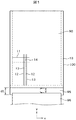
- FIG. 1 is a plan view of an organic EL display device having a flexible substrate 100 to which the present invention is applied.
- the flexible panel device of the present invention is assumed to be curved in the terminal region 95, but FIG. 1 is a developed view before bending the terminal region 95. Since the flexible panel device of FIG. 1 is curved in the terminal region 95, the length dt of the terminal region 150 is longer than usual.
- scanning lines 11 extend in the horizontal direction (x direction) and are arranged in the vertical direction (y direction).
- the video signal lines 12 extend in the vertical direction and are arranged in the horizontal direction.
- the power supply lines 13 extend in the vertical direction and are arranged in the horizontal direction.
- Pixels 14 are formed in a region surrounded by the video signal line 12 and the scanning line 11 or the power supply line 13 and the scanning line 11.
- Scanning line drive circuits 18 are formed by TFTs on both sides of the display area 90.
- the terminal wiring extending from the display area 90 extends in the vertical direction, and is connected to the flexible wiring board 96 at the end of the terminal area.
- the driver IC that drives the video signal line 12 and the like is mounted on the flexible wiring board 96.
- the video signal from the driver IC is transmitted to the video signal line 12 via the terminal wiring of the terminal region 95. Therefore, in the terminal region 95, a large number of terminal wirings drawn from the video signal line 12 extend in the vertical direction (y direction).
- the display area 90 becomes high definition, the density of the terminal wiring also increases.
- a selective switching circuit is provided between the display area 90 and the terminal area 95 to reduce the number of leader lines to, for example, about 1/3 of the number of video signal lines in the display area.
- the configuration is taken. Even so, if the pixel spacing in the horizontal direction (x direction) in the display area 90 is, for example, 30 ⁇ m, the wiring spacing in the horizontal direction in the terminal area 95 is very small, about 90 ⁇ m. Then, the wiring width becomes small, and if the terminal region 95 is bent, there is a risk of disconnection.
- the terminal wiring is generally made of the same material as the video signal line.
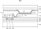
- FIG. 2 is a cross-sectional view showing a cross-sectional configuration of a pixel portion in a display area of an organic EL display device.
- an organic base film 101 also formed of polyimide is formed on the TFT substrate 100 made of a resin such as polyimide. This is to flatten the surface.
- the thickness of the TFT substrate 100 is, for example, 20 ⁇ m, and the thickness of the organic base film 101 is, for example, 2 ⁇ m.
- the inorganic base film 102 is formed on the organic base film 101.
- the role of the inorganic base film 102 is that moisture and impurities from the TFT substrate 100 or the organic base film 101 formed of resin are formed on the semiconductor layer 103 or the semiconductor layer 103 formed on the inorganic base film 102. This is to prevent transmission to the organic EL layer 113.
- As the inorganic base film 102 a laminated structure of a silicon oxide (hereinafter referred to as SiO) film and a silicon nitride (hereinafter referred to as SiN) film is used.
- the oxide semiconductor 103 constituting the TFT is formed on the inorganic base film 102.
- the oxide semiconductor 103 is an example, and a TFT using a polysilicon semiconductor may be used.
- a connection electrode 104 is formed of metal in the drain region and the source region of the oxide semiconductor 103.
- a gate insulating film 105 is formed over the oxide semiconductor 103, and a gate electrode 106 is formed on the gate insulating film 105.
- An interlayer insulating film 107 is formed so as to cover the gate electrode 106. Through holes are formed in the interlayer insulating film 107 and the gate insulating film 105, and the oxide semiconductor 103, the drain electrode 108, and the source electrode 109 are connected through the through holes. In many cases, the drain electrode 108 also serves as the video signal line 12 shown in FIG.
- An organic passivation film 110 made of polyimide or the like is formed so as to cover the drain electrode 108 and the source electrode 109.
- the organic passivation film 110 extends to the terminal region and becomes a first organic passivation film 30 that protects the terminal wiring 20.
- a lower electrode 111 serving as an anode for the organic EL layer is formed on the organic passivation film 110.
- the source electrode 109 is connected to the lower electrode 111 via a through hole 1101 formed in the organic passivation film 110.
- a bank 112 made of polyimide is formed so as to cover the periphery of the lower electrode 111.
- the bank 112 is formed by first forming polyimide on the entire surface and then patterning it by photolithography to form holes 1121. Then, a light emitting layer 113 made of organic EL is formed in the hole 1121. The portion other than the hole 1121 becomes the bank 112.
- the bank 112 made of polyimide is formed, and at the same time, the second organic passivation film 40 that protects the terminal wiring 20 in the terminal region 95 is formed.
- the role of the bank 112 is to prevent the organic EL layer 113 from being stepped by the end of the lower electrode 111. Therefore, the bank 112 covers the end of the lower electrode 111.
- the organic EL layer 113 is formed on the lower electrode 111, and the upper electrode 114 serving as a cathode is formed on the organic EL layer 113 by a transparent conductive film such as ITO (Indium, Tin, Oxide).
- a protective film 115 is formed to protect the organic EL layer 113 from moisture and the like from the outside.
- the protective film 115 is formed of, for example, a laminated film of an inorganic film such as SiN and an organic film such as polyimide or acrylic.
- a circularly polarizing plate 117 is attached to cover the protective film 112 via an adhesive material 116. The role of the circularly polarizing plate 117 is to prevent reflection of external light.
- the organic base film 101 extends to the terminal region 95, and the video signal line 12 extends to the terminal region 95 to form the terminal wiring 20.
- the organic passivation film 110 extends to the terminal region 95 to become the first organic passivation film 110, and protects the terminal wiring 20.
- the polyimide constituting the bank 112 also extends to the terminal region 95 and serves as a second organic passivation film 40 for protecting the terminal wiring 20.
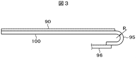
- FIG. 3 is a cross-sectional view showing a state in which the organic EL display device of FIG. 1 is bent in the terminal region 95.
- the display area 90 is formed with the TFTs constituting the pixels, the organic EL light emitting element, the video signal line 12, the scanning line 11, the power supply line 13, and the like described in FIGS. 1 and 2. Both the terminal area 95 and the display area 90 are formed on the same TFT substrate 100.
- a flexible wiring board 96 is connected to the end of the terminal region.
- the driver IC is mounted on the flexible wiring board 96.
- the TFT substrate 100 is made of a resin such as polyimide having a thickness of about 20 ⁇ m, it can be curved with a very small radius of curvature R.
- the value of R can be, for example, 100 ⁇ m or less.
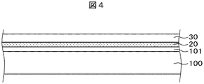
- FIG. 4 is an example of a cross-sectional view of the terminal region 95 before bending. That is, FIG. 4 corresponds to a YY cross-sectional view of the terminal region 95 of FIG.
- an organic base film 101 made of polyimide is formed on the TFT substrate 100 made of polyimide.
- the terminal wiring 20 is formed on the organic base film 101, and the terminal wiring 20 is simultaneously formed of the same material as the video signal line 12 in the display area 90.
- the first organic passivation film 30 covers the terminal wiring 20 and is formed of the same polyimide as the organic passivation film 110 in the display region 95. This is to protect the terminal wiring 20.
- FIG. 5 is a cross-sectional view for explaining the stress when the plate-shaped structure is curved.
- the sample of FIG. 5 is an example in which a plate having a thickness of t is curved in ⁇ radians.
- the radius of curvature of the so-called neutral plane MN is Rm.
- the neutral surface MN is a surface to which neither compressive stress nor tensile stress is applied when the plate is curved.
- the position of ⁇ from the inner surface AB is the neutral plane. If the sample is a single piece of uniform material, the neutral plane MN will be approximately central in the plate thickness direction.
- Formula 1 is a formula for obtaining a neutral surface when the plate-like structure is composed of a plurality of layers and n layers.
- Equation 1 ⁇ is the distance from the inner surface to the neutral surface.
- E is the Young's modulus of the i layer, hi is the distance from the inner surface to the i layer, and ti is the film thickness of the i layer.
- the most serious problem in the terminal area 95 is that the terminal wiring 20 is broken by bending the terminal area 95.
- the terminal wiring 20 is configured so that stress is not applied as much as possible. That is, it is preferable to arrange the terminal wiring 20 so as to be close to the neutral surface.
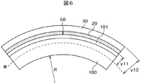
- FIG. 6 is a cross-sectional view of the terminal region 95 shown in FIG. 4 when the inner surface is curved with the radius of curvature of R.
- the neutral plane is represented by a dotted line M.
- the neutral surface M exists in the substrate 100.
- the thickness of the TFT substrate 100 is 20 ⁇ m
- the thickness of the first organic passivation film 30 covering the terminal wiring 20 is about 2 ⁇ m. Therefore, y11 in FIG. 6 has a relatively large value and is relatively large for the terminal wiring 20. A large tensile stress is applied. Therefore, in FIG. 6, a crack 50 is generated in the terminal wiring 20.
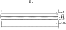
- FIG. 7 shows a configuration in which the second organic passivation film 40 is formed on the first organic passivation film 30 in the terminal region with the same material as the bank 112 in the display region 90, for example, polyimide, in order to deal with this. It is a sectional view. Note that FIG. 7 corresponds to a YY cross-sectional view of the terminal region 95 of FIG. Since the second organic passivation film 40 can be formed at the same time as forming the bank 112 of the display region 90, it does not become a process load. As a result, when the terminal region 95 is curved, the position of the terminal wiring 20 can be brought closer to the neutral surface M.
- FIG. 8 is a cross-sectional view showing a state in which the terminal region having the configuration of FIG. 7 is curved so that the inner surface has a radius of curvature R.
- the distance between the neutral surface M and the terminal wiring 20 is y21, which is smaller than y11 in the case of FIG. Therefore, the probability that the terminal wiring 20 will be the starting point of the crack is reduced.
- the distance y22 between the outer surface of the second organic passivation film 40 and the neutral line M is larger than the distance y12 between the outer surface of the first organic passivation film 30 and the neutral line M in the case of FIG. Therefore, in the configuration of FIG. 7, there is a risk that cracks due to tensile stress will occur in the second organic passivation film 40 when it is curved.
- FIG. 8 is a cross-sectional view showing a state in which a crack 50 is generated in the second organic passivation film 40 due to tensile stress. If the crack 50 is stopped by the second organic passivation film 40, it does not pose a big problem, but the crack may propagate to the first organic passivation film 30 and further to the terminal wiring 20. In that case, the terminal wiring 20 will be disconnected.
- FIG. 9 is a plan view of an organic EL display device for explaining the first embodiment of the present invention.
- the terminal area 95 is enlarged and described as compared with the case of FIG.
- a plurality of terminal wirings 20 extend vertically in the terminal area 95, connecting the display area 90 and the flexible wiring board 96.
- the region surrounded by the alternate long and short dash line in FIG. 9 indicates the bent region BA.
- a large number of terminal wirings 20 extend in the terminal area 95, but in FIG. 9, only a few terminal wirings 20 are shown for the sake of clarity.
- FIG. 10 is an enlarged plan view of the terminal wiring 20 portion of the terminal region 95 of FIG. 9 in the first embodiment.
- the terminal wirings 20 are arranged at a predetermined pitch, and the second organic passivation film 40 is formed in a stripe shape so as to cover the terminal wirings 20. That is, the feature of the first embodiment is that the second organic passivation film 40 is not formed on the entire surface of the terminal region 95, but is formed along the terminal wiring so as to cover the terminal wiring 20. ..
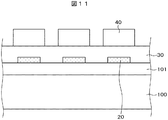
- FIG. 11 is a sectional view taken along line BB of FIG.
- the organic base film 101 is formed on the TFT substrate 100
- the terminal wiring 20 is formed on the terminal wiring 20
- the first organic passivation film 30 is formed over the terminal wiring 20 as in FIG. 7.
- the feature of FIG. 11 is that the second organic passivation film 40 is not formed on the entire surface of the terminal region, but is patterned along the terminal wiring 20. By patterning the second organic passivation film 40, the tensile stress related to the second organic passivation film 40 can be reduced. As a result, cracks that occur in the second organic passivation film 40 can be prevented, and by extension, disconnection of the terminal wiring 20 can be prevented.
- the width of the second organic passivation film 40 formed on the terminal wiring 20 is larger than the width of the terminal wiring 20. This is so that the second organic passivation film 40 is present on the terminal wiring 20 even if a manufacturing error occurs. This is because it is more preferable that the organic passivation film 40 is formed on the terminal wiring 20 in terms of relaxing the tensile stress on the terminal wiring 20.
- FIG. 11 shows an example in which the second organic passivation film 40 is formed along the terminal wiring 20, but is not limited to the configuration of FIG. 11 in the sense of reducing the stress generated in the second organic passivation film 40. It may have a configuration of 12 or the like.
- FIG. 12 shows an example in which the spacing between the striped patterns of the second organic passivation film 40 is matched with the spacing between the terminal wirings 20, but the arrangement position of the second organic passivation film 40 is not on the terminal wiring 20. Is. Further, although the width of the first organic passivation film 40 in FIG. 12 is the same as the width of the terminal wiring 20, a predetermined effect can be expected regardless of whether the width is wider or narrower than the terminal wiring 20. You can.
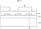
- FIG. 13 is another example of the striped pattern of the second organic passivation film 40.
- the spacing and width between the second organic passivation films 40 are not synchronized with the spacing and width of the terminal wiring 20. Since patterning the second organic passivation film 40 reduces the tensile stress applied to the terminal wiring 20, the spacing, position, width, etc. of the stripe pattern of the second organic passivation film 40 are the same as those of the terminal wiring 20. The shape should be the one that reduces stress most.
- the top layer uses a SiN film 60 instead of an organic film. This is because the SiN film 60 is hard, so that it is more easily cracked than the organic film, and the effect can be easily confirmed.
- FIG. 14 is a sample as a comparative example, in which the organic base film 101 is formed on the TFT substrate 100, and the terminal wiring 20 is formed on the organic base film 101.
- the uppermost layer uses a SiN film 60, which is an inorganic film.
- the TFT substrate 100 is 20 ⁇ m
- the organic base film 101 is 2 ⁇ m
- the first organic passivation film 30 is 2 ⁇ m
- the SiN film 60 is 200 nm.
- the terminal wiring 20 is configured such that the aluminum alloy film 22 is sandwiched between the Ti film 21 and the Ti film 23.
- the thickness of the aluminum alloy film 22 is 500 nm, the thickness of the Ti film 21 is 100 nm, and the thickness of the Ti film 23 is 100 nm.
- the SiN film 60 which is the uppermost layer in FIG. 16, is formed in a planar shape.
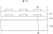
- FIG. 16 is an example in which the uppermost SiN film 60 is patterned along the terminal wiring 20.
- the cross-sectional structure of each layer except the SiN film 60 is the same as in FIGS. 14 and 15.
- the SiN film 60 is formed with the same width and the same interval as the terminal wiring 20.
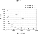
- FIG. 17 is a result of evaluating the strain generated in the SiN film 60 with respect to the size of the bending radius when the samples of FIGS. 14 to 16 are curved.
- the horizontal axis is the bending radius ( ⁇ m) and the vertical axis is the strain (%).
- the straight line A1 shown by the dotted line indicates the radius of curvature in which the SiN film 60, which is the uppermost layer, is cracked in the sample shown in FIG. As shown in FIG. 18, this state is the position where the crack 50 is generated only in the SiN film 60.
- the bending radius in this case is about 1000 ⁇ m, and the SiN film 60 is distorted by about 1.0%.
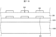
- the straight line B1 shown by the dotted line indicates the radius of curvature in which the SiN film 60, which is the uppermost layer, is cracked in the sample shown in FIG. As shown in FIG. 19, this state is a position where cracks are generated only in the SiN film 60.
- the bending radius in this case is about 600 ⁇ m, and the SiN film 60 is distorted by about 1.0%.
- the SiN film 60 is cracked when the SiN film 60 is in a state of being distorted by about 1.0% regardless of the shape.
- the SiN film 60 is changed from a solid film as shown in FIG. 14 to a patterning shape along the terminal wiring 20 as shown in FIG. 16, the SiN film 60 is less likely to be distorted, and the bending radius at which cracks do not occur is reduced to about. It can be reduced from 1000 ⁇ m to about 600 ⁇ m.
- the data shown in FIG. 17 shows the case where the protective film of the uppermost layer is a SiN film, but the same tendency is obtained even if the uppermost layer is an organic film.
- FIG. 20 is a plan view of the organic EL display device according to the second embodiment.
- the difference between FIG. 20 and FIG. 9 is that the terminal wiring 20 in the terminal region 95 has a zigzag shape.
- the stress generated in the terminal wiring 20 can be relaxed, and the probability of disconnection of the terminal wiring 20 can be reduced.
- the present invention can also be applied to the configuration as shown in FIG. 20, and the probability of disconnection of the terminal wiring 20 can be further reduced.
- FIG. 21 is an enlarged plan view of the terminal wiring 20 in the terminal region 95 of FIG. 20.
- the terminal wirings 20 extend in a zigzag manner in the vertical direction (y direction) and are arranged in the horizontal direction (x direction).
- the second organic passivation film 40 covers the terminal wiring 20 and extends in a zigzag manner along the terminal wiring 20 in the vertical direction (y direction) and is arranged in the horizontal direction (x direction).
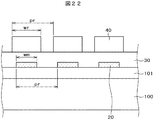
- FIG. 22 is a cross-sectional view taken along the line CC of FIG.
- the shape of FIG. 22 is the same as that of FIG. 11 of the first embodiment, and the relationship between the interval pr of the terminal wiring 20 and the width wm of the terminal wiring 20 and the width wr and the interval pr of the second organic passivation film 40 is the same as in FIG. Is.
- the probability of disconnection of the terminal wiring 20 can be significantly reduced by applying the present invention.
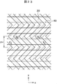
- FIG. 23 shows an enlarged plan view of the terminal wiring 20 in the third embodiment.
- the pattern of the second organic passivation film 40 in the terminal region 95 is different from that of Example 2.
- the second organic passivation film 40 extends in the lateral direction (x direction) so as to cover the bent portion of the zigzag-shaped terminal wiring 20, and the bent portion of the terminal wiring 20 has a zigzag shape. They are arranged in the vertical direction (y direction) according to the interval pv.
- FIG. 24 is a cross-sectional view taken along the line DD of FIG.
- FIG. 24 is a cross-sectional view of a bent portion of the terminal wiring 20, which is entirely covered with a second organic passivation film 40.
- FIG. 25 is a cross-sectional view taken along the line EE of FIG. This portion is not covered by the second organic passivation film 40.
- the terminal region 95 is curved, the greatest stress is generated at the bent portion of the terminal wiring 20 having a zigzag pattern. Therefore, by covering this bent portion with the second organic passivation film 40, the position of the neutral surface of this portion can be raised, and as a result, the probability of disconnection of the terminal wiring 20 can be reduced.
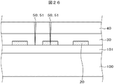
- FIG. 26 is a cross-sectional view showing this situation.
- the first organic passivation film 30 is formed so as to cover the terminal wiring 20, and the second organic passivation film 40 is formed on the first organic passivation film 30.
- a scratch 51 or a crack 50 is generated due to handling or the like, which propagates to the terminal wiring 20 after bending the terminal region and causes the terminal wiring 20 to be disconnected. It is unknown where the scratch 51 or the crack 50 due to such handling or the like occurs. In FIG. 26, since these are generated on the terminal wiring 20, this is an example of propagating to the disconnection of the terminal wiring 20. On the other hand, if the scratch 51 or the crack 50 in the second organic passivation film occurs in a place where there is no terminal wiring 20 when viewed in a plane, there is no direct effect on the terminal wiring 20 and the terminal wiring 20 is disconnected. Nor.
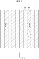
- FIG. 27 is an enlarged plan view of the terminal region 95 in the fourth embodiment.
- the plan view of the organic EL display device in the fourth embodiment has the same shape as that of FIG.
- the terminal wirings 20 extend in the vertical direction (y direction) and are arranged in the horizontal direction (x direction).
- the second organic passivation film 40 is formed between the terminal wiring 20 and the terminal wiring 20 and does not cover the terminal wiring 20.
- FIG. 28 is a sectional view taken along line FF of FIG. 27.
- the second organic passivation film 40 is not formed on the terminal wiring 20, but is formed in a place where the terminal wiring 20 does not exist.
- the interval pr of the second organic passivation film 40 is about 0.1 mm, and the interval of the terminal wiring 20 is formed at 0.05 mm, which is half of the interval pr. That is, the organic passivation film 40 can be formed between the wirings of the terminal wiring 20.
- Example 1 to 4 the present invention has been described for an organic EL display device. However, the present invention can be similarly applied to a liquid crystal display device and a sensor device that two-dimensionally senses fingerprints, veins, tactile sensations, etc. when a flexible substrate is used.
Landscapes
- Physics & Mathematics (AREA)
- Nonlinear Science (AREA)
- General Physics & Mathematics (AREA)
- Mathematical Physics (AREA)
- Chemical & Material Sciences (AREA)
- Crystallography & Structural Chemistry (AREA)
- Optics & Photonics (AREA)
- Engineering & Computer Science (AREA)
- Theoretical Computer Science (AREA)
- Devices For Indicating Variable Information By Combining Individual Elements (AREA)
- Electroluminescent Light Sources (AREA)
- Liquid Crystal (AREA)
Abstract
本発明の目的は、端子領域を折り曲げて使用されるフレキシブル表示装置において、折り曲げ部における端子配線の断線を防止することである。このために、本発明は、例えば次のよう構成をとる。湾曲可能な基板(100)に表示領域と端子領域が形成された表示装置であって、前記端子領域は他の配線基板と接続する端部を有し、前記端子領域には、端子配線(20)が前記表示領域から前記端部に向かう第1の方向に延在し、かつ、前記第1の方向と交差する方向である第2の方向に配列し、前記端子配線(20)を覆って第1有機パッシベーション膜(30)が形成され、前記第1有機パッシベーション膜(30)の上には、第2有機パッシベーション膜(40)が形成され、前記第2有機パッシベーション膜(40)は、前記第1の方向に延在し、前記第2の方向に配列するようにパターニングされていることを特徴とする表示装置。
Description
本発明は表示装置やセンサ装置に係り、特に基板を湾曲させることができるフレキシブルパネル装置に関する。
有機EL表示装置や液晶表示装置などの表示装置、および、指紋や静脈、或いは触覚などを2次元的にセンシングするセンサ装置などは、フレキシブルに湾曲させて使用するものがある。この場合、パネルを形成する基板を薄いガラスあるいは薄い樹脂によって形成する。特にポリイミド等の樹脂を基板に用いることによって、よりフレキシブルなパネルを実現することが出来る。
フレキシブルパネル装置には、TFT(Thin Film Transistor)、配線、これらを保護する保護絶縁膜等、種々の素子が存在する。パネルを湾曲すると、これらの素子にも応力が加わり、固い素子の場合は、割れる恐れがある。これを防止するためには、パネルを湾曲した場合に、各素子に加わる曲げ応力を抑制することが望ましい。
特許文献1には、表示装置を湾曲して使用する場合、これらの素子に曲げ応力が加わることを抑制するために、フィルム状の基板表面に形成される配線等を覆って、他のフィルムを形成し、応力のバランスが取れた位置となる、いわゆる中立面を移動させることによって、湾曲した場合に、配線等に引っ張り応力あるいは、圧縮応力のいずれもかからないようにする構成が記載されている。
表示装置やセンサ装置では、薄くすることとともに、外形を大きくしないことが求められている。これらの装置は、表示領域または検出領域と、外部と信号をやり取りするための端子が形成される端子領域に分かれている。フレキシブルパネル装置では、表示領域または検出領域を最大化するため、一般的には、背面に端子が来るように、端子領域で基板を折り曲げる。基板をポリイミド等による樹脂基板で形成することによって、小さな半径で折り曲げることが出来る。しかし、端子領域には、表示領域や検出領域から延設された端子配線が形成されており、端子配線に曲げによる大きな応力が加わると断線する危険がある。
本発明の目的は、基板を端子領域において折り曲げた場合にも、端子配線に断線が生じない、信頼性の高い表示装置を実現することである。本発明の他の目的は、端子配線を覆う、有機絶縁膜等で形成された保護層に傷等が生じた場合にも、この傷が内部に伝搬して端子配線の断線を生じさせることを防止することである。
本発明は上記課題を克服するものであり、代表的な手段は次のとおりである。すなわち、湾曲可能な基板に表示領域と端子領域が形成された表示装置であって、前記端子領域は他の配線基板と接続する端部を有し、前記端子領域には、端子配線が前記表示領域から前記端部に向かう第1の方向に延在し、かつ、前記第1の方向と交差する方向である第2の方向に配列し、前記端子配線を覆って第1有機パッシベーション膜が形成され、前記第1有機パッシベーション膜の上には、第2有機パッシベーション膜が形成され、前記第2有機パッシベーション膜は、前記第1の方向に延在し、前記第2の方向に配列するようにパターニングされていることを特徴とする表示装置、である。
以下に実施例を用いて本発明の内容を詳細に説明する。以下の説明では、主に、有機EL表示装置を例にとって本発明を説明するが、本発明は、液晶表示装置等、他の表示装置や、指紋や静脈などを2次元的に検出するセンサ装置にも適用することが出来る。
図1は本発明が適用されるフレキシブル基板100を有する有機EL表示装置の平面図である。本発明のフレキシブルパネル装置は、端子領域95において湾曲することを想定しているが、図1は、端子領域95を湾曲する前の展開図となっている。図1のフレキシブルパネル装置は、端子領域95で湾曲するので端子領域150の長さdtが通常より長い構成となっている。
図1において、表示領域90には、走査線11が横方向(x方向)に延在し、縦方向(y方向)に配列している。映像信号線12が縦方向に延在し、横方向に配列している。また、電源線13が縦方向に延在し、横方向に配列している。映像信号線12と走査線11、あるいは、電源線13と走査線11で囲まれた領域に画素14が形成されている。表示領域90の両サイドには走査線駆動回路18がTFTによって形成されている。
端子領域95には、表示領域90から延設された端子配線が縦方向に延在し、端子領域の端部において、フレキシブル配線基板96と接続している。映像信号線12等を駆動するドライバICはフレキシブル配線基板96に搭載されている。例えば、ドライバICからの映像信号は、端子領域95の端子配線を経由して、映像信号線12に伝達される。したがって、端子領域95には、映像信号線12から引き出された非常に多くの端子配線が縦方向(y方向)に延在している。表示領域90が高精細になると、この端子配線の密度も増大する。
端子配線の密度を減らすために、表示領域90と端子領域95との間に、選択スイッチング回路を設けて、引出し線の数を例えば、表示領域の映像信号線の数の1/3程度に低減する構成がとられる。それでも、表示領域90における横方向(x方向)の画素間隔が例えば30μmとすると、端子領域95の横方向の配線間隔は、90μm程度と非常に小さいものとなる。そうすると、配線幅も小さくなり、端子領域95を折り曲げると断線の危険が生ずる。なお、端子配線は、一般には、映像信号線と同じ材料で形成される。
図2は、有機EL表示装置の表示領域における画素部分の断面構成を示す断面図である。図2において、例えばポリイミド等の樹脂で形成されたTFT基板100の上に、やはりポリイミドで形成された有機下地膜101を形成する。表面を平坦化するためである。TFT基板100の厚さは例えば20μm、有機下地膜101の厚さは例えば2μmである。
有機下地膜101の上に無機下地膜102が形成される。無機下地膜102の役割は、樹脂で形成されたTFT基板100あるいは、有機下地膜101からの水分や不純物が、無機下地膜102の上に形成される半導体層103あるいは、その上に形成される有機EL層113に対して伝わらないようにするためである。無機下地膜102は、酸化シリコン(以後SiOと呼ぶ)膜と窒化シリコン(以後SiNと呼ぶ)膜の積層構造が用いられる。
無機下地膜102の上にTFTを構成する酸化物半導体103が形成されている。酸化物半導体103は例であって、ポリシリコン半導体を用いたTFTでも良い。酸化物半導体103のドレイン領域及びソース領域には、接続電極104が金属によって形成されている。酸化物半導体103を覆って、ゲート絶縁膜105が形成され、その上にゲート電極106が形成されている。
ゲート電極106を覆って層間絶縁膜107が形成される。層間絶縁膜107及びゲート絶縁膜105にスルーホールを形成し、このスルーホールを介して酸化物半導体103とドレイン電極108及びソース電極109を接続する。ドレイン電極108は図1に示す映像信号線12が兼ねている場合が多い。
ドレイン電極108及びソース電極109を覆ってポリイミド等で形成された有機パッシベーション膜110が形成される。有機パッシベーション膜110は、端子領域に延在し、端子配線20を保護する第1有機パッシベーション膜30になる。有機パッシベーション膜110の上に有機EL層に対するアノードとなる下部電極111が形成される。ソース電極109は有機パッシベーション膜110に形成されたスルーホール1101を介して下部電極111と接続する。
下部電極111の周辺を覆うようにポリイミドによるバンク112を形成する。バンク112は、まず、ポリイミドを全面に形成した後、フォトリソグラフィによって、パターニングし、ホール1121を形成することによって形成する。そして、このホール1121内に有機ELによる発光層113が形成される。ホール1121以外の部分がバンク112になる。なお、本発明では、ポリイミドによるバンク112を形成すると同時に、端子領域95において端子配線20を保護するける第2有機パッシベーション膜40を形成する。
バンク112の役割は、下部電極111の端部によって有機EL層113が段切れを生ずることを防止することである。したがって、バンク112は下部電極111の端部を覆っている。ホール1121内において、下部電極111の上に有機EL層113が形成され、その上にカソードとなる上部電極114が、ITO(Indium、Tin、Oxide)等の透明導電膜によって形成される。有機EL層113を外部からの水分等から保護するための、保護膜115が形成される。保護膜115は、例えば、SiN等の無機膜及びポリイミドあるいはアクリル等の有機膜の積層膜によって形成される。保護膜112を覆って円偏光板117が粘着材116を介して貼り付けられている。円偏光板117の役割は、外光の反射を防止することである。
図2で説明した構成において、有機下地膜101は端子領域95に延在し、映像信号線12は端子領域95に延在して、端子配線20となる。そして、有機パッシベーション膜110は端子領域95に延在して第1有機パッシベーション膜110となり、端子配線20を保護する。また、本発明においては、バンク112を構成するポリイミドも端子領域95に延在し、端子配線20を保護するための第2有機パッシベーション膜40となる。
図3は、図1の有機EL表示装置を端子領域95において折り曲げた状態を示す断面図である。図3において、表示領域90には、図1、図2で説明した、画素を構成するTFT、有機EL発光素子、映像信号線12、走査線11、電源線13等が形成されている。端子領域95、表示領域90とも、同じTFT基板100に形成されている。端子領域端部には、フレキシブル配線基板96が接続している。ドライバICはフレキシブル配線基板96に搭載されている。
TFT基板100は、厚さが20μm程度のポリイミド等の樹脂で形成されているので、非常に小さな曲率半径Rで湾曲することが可能である。Rの値は、例えば、100μm以下とすることが出来る。このような小さな曲率半径で湾曲させると、TFT基板100の外側には大きな引っ張り応力が生じ、内側には大きな圧縮応力が生じる。
図4は、折り曲げる前の端子領域95の断面図の例である。すなわち、図4は、図1の端子領域95のY-Y断面図に相当する。図4において、ポリイミドで形成されたTFT基板100の上に、ポリイミドによる有機下地膜101が形成されている。有機下地膜101の上に端子配線20が形成されている、端子配線20は、表示領域90の映像信号線12と同じ材料によって同時に形成される。端子配線20を覆って第1有機パッシベーション膜30が、表示領域95における有機パッシベーション膜110と同じポリイミドによって形成されている。端子配線20を保護するためである。
図5は、板状の構造を湾曲させた場合のストレスを説明する断面図である。図5のサンプルは、厚さtの板が、θラジアンで湾曲している例である。図5において、いわゆる中立面MNの曲率半径はRmである。中立面MNは、板を湾曲した場合に、圧縮応力も引張り応力もかからない面である。図5において、内表面ABからλの位置が中立面となっている。サンプルが1枚の均一な材料であれば、中立面MNは、ほぼ板厚方向の中央部になる。
図5において、面PQは中立面MNよりも外表面CDにyだけ近づいているので、PQ面には引っ張り応力が加わることになる。この時のPQ面における歪εの値は、ε=y/Rmである。なお、歪は無単位である。
数式1は、板状構造が複数層、n層で構成されている場合の中立面を求める式である。
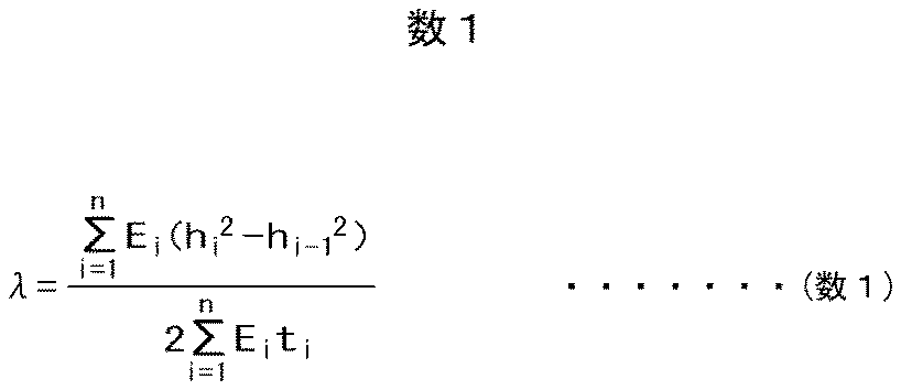
数式1において、λは内表面から中立面までの距離である。Eiはi層のヤング率、hiは内表面からi層までの距離、tiはi層の膜厚である。
端子領域95における最も深刻な問題は、端子領域95を折り曲げることによって、端子配線20が断線することである。これを防ぐためには、端子配線20はできるだけ応力が加わらない構成とするのが良い。つまり、端子配線20が中立面に近くなるように、配置するのが良い。
図6は、図4に示す端子領域95を内表面がRの曲率半径で湾曲させた場合の断面図である。図6において、中立面は点線Mで表している。中立面Mは、基板100内に存在している。図6において、TFT基板100の厚さは20μm、端子配線20を覆う第1有機パッシベーション膜30の厚さは約2μmなので、図6におけるy11は比較的大きな値となり、端子配線20には比較的大きな引っ張り応力が加わっている。このため、図6では、端子配線20にクラック50が発生している。
図7は、これを対策するために、端子領域において、第1有機パッシベーション膜30の上に、表示領域90におけるバンク112と同じ材料、例えばポリイミドによって第2有機パッシベーション膜40を形成した構成を示す断面図である。なお、図7は、図1の端子領域95のY-Y断面図に相当する。第2有機パッシベーション膜40は表示領域90のバンク112を形成すると同時に形成できるので、プロセス負荷になることは無い。これによって端子領域95を湾曲させた際に、端子配線20の位置を、中立面Mに、より近づけることが出来る。
図8は、図7の構成の端子領域を内表面が曲率半径Rになるように湾曲させた状態を示す断面図である。図8において、中立面Mと、端子配線20の距離は、y21であり、図6の場合のy11よりも小さくなっている。したがって、端子配線20がクラックの起点となる確率は低下する。
しかしながら、第2有機パッシベーション膜40の外表面と中立線Mとの距離y22が図6の場合における、第1有機パッシベーション膜30の外表面と中立線Mとの距離y12よりも大きくなっている。したがって、図7の構成では、湾曲した場合に第2有機パッシベーション膜40に引張り応力によるクラックが発生する危険が生ずる。
図8は、第2有機パッシベーション膜40に引張り応力によってクラック50が発生した状態を示す断面図である。クラック50が第2有機パッシベーション膜40にて止まっていれば、大きな問題にならないが、このクラックは、第1有機パッシベーション膜30、さらには、端子配線20に伝搬する場合がある。その場合、端子配線20に断線が発生することになる。
図9は、本発明の実施例1を説明するための有機EL表示装置の平面図である。図9では、図1の場合に比較して、端子領域95を拡大して記載している。図9において、端子領域95に複数の端子配線20が縦方向に延在し、表示領域90とフレキシブル配線基板96とを接続している。図9における一点鎖線で囲った領域は、折り曲げ領域BAを示す。実際の製品においては、端子領域95には多数の端子配線20が延在しているが、図9では、わかり易くするために、わずかの端子配線20しか記載していない。
図10は、実施例1における、図9の端子領域95の端子配線20部分の拡大平面図である。図10において、端子配線20が所定のピッチで配列し、端子配線20を覆うように、第2有機パッシベーション膜40がストライプ状に形成されている。つまり、実施例1の特徴は、第2有機パッシベーション膜40は、端子領域95全面に形成されているのではなく、端子配線20を覆うように、端子配線に沿って形成されていることである。
図11は図10のB-B断面図である。図11において、TFT基板100の上に有機下地膜101が形成され、その上に端子配線20が形成され、これを覆って第1有機パッシベーション膜30が形成されていることは、図7と同じである。図11の特徴は、第2有機パッシベーション膜40を、端子領域全面に形成するのではなく、端子配線20に沿ってパターニングしていることである。第2有機パッシベーション膜40をパターニングすることによって、第2有機パッシベーション膜40に係る引張り応力を軽減することができる。これによって、第2有機パッシベーション膜40に生ずるクラックを防止することが出来、ひいては、端子配線20の断線も防止することが出来る。
図10及び図11においては、端子配線20の上に形成する第2有機パッシベーション膜40の幅は、端子配線20の幅よりも大きくなっている。製造誤差が生じても、第2有機パッシベーション膜40が端子配線20の上に存在させるようにするためである。端子配線20に対する引っ張り応力を緩和させる意味では、端子配線20の上に有機パッシベーション膜40が形成されていたほうが、より好ましいからである。
図11は、第2有機パッシベーション膜40を端子配線20に沿って形成した例であるが、第2有機パッシベーション膜40に発生するストレスを軽減するという意味では、図11の構成に限らず、図12等の構成でもよい。図12は、第2有機パッシベーション膜40のストライプ状のパターン間の間隔は、端子配線20間の間隔と合わせているが、第2有機パッシベーション膜40の配置位置は、端子配線20上ではない例である。また、図12における第1有機パッシベーション膜40の幅は、端子配線20の幅と同じになっているが、端子配線20の幅より広い場合でも、狭い場合でも、所定の効果は期待することが出来る。
図13は、第2有機パッシベーション膜40のストライプ状のパターンの他の例である。図13は、第2有機パッシベーション膜40間の間隔も幅も、端子配線20の間隔や幅と同期をとっているわけではない。第2有機パッシベーション膜40をパターニングするということが、端子配線20に掛かる引張り応力を軽減することになるので、第2有機パッシベーション膜40のストライプパターンの間隔、位置、幅等は、端子配線20のストレスを最も軽減する形状にすればよい。
図14乃至図19は、実施例1のように、最上層の層をパターニングすることが、実際に最上層のストレスの緩和になることを実証するための説明図である。実験及びシミュレーションでは、最上層は、有機膜の代わりに、SiN膜60を用いている。SiN膜60は硬いので、有機膜よりもクラックし易く、効果の確認が容易だからである。
図14は比較例としてのサンプルであり、TFT基板100の上に有機下地膜101を形成し、有機下地膜101の上に端子配線20を形成している。最上層は、図11等とは異なり、無機膜であるSiN膜60を使用している。TFT基板100は20μm、有機下地膜101は2μm、第1有機パッシベーション膜30は2μm、SiN膜60は200nmである。端子配線20の構成は、図15に示すように、アルミ合金膜22をTi膜21及びTi膜23でサンドイッチする構成となっている。アルミ合金膜22の厚さは500nm、Ti膜21の厚さは100nm、Ti膜23の厚さは100nmである。図16における最上層であるSiN膜60は平面状に形成されている。
図16は、最上層のSiN膜60を端子配線20に沿ってパターニングした例である。図8において、SiN膜60を除く各層の断面構成は、図14、図15と同じである。図16において、SiN膜60は端子配線20と同じ幅、同じ間隔で形成されている。
図17は、図14乃至図16のサンプルを湾曲させた場合に、曲げ半径の大きさに対して、SiN膜60に発生する歪を評価した結果である。図17において、横軸は曲げ半径(μm)であり、縦軸は歪(%)である。
図17において、点線で示す直線A1は、図14に示すサンプルにおいて、最上層であるSiN膜60にクラックが発生した曲率半径を示している。この状態は、図18に示すように、SiN膜60にのみクラック50が発生した状態の位置である。この場合の曲げ半径は、約1000μmであり、SiN膜60には、約1.0%の歪が発生している。
図17において、点線で示す直線B1は、図16に示すサンプルにおいて、最上層であるSiN膜60にクラックが発生した曲率半径を示している。この状態は、図19に示すように、SiN膜60にのみクラックが発生した状態の位置である。この場合の曲げ半径は、約600μmであり、SiN膜60には、約1.0%の歪が発生している。このように、図17の結果から、SiN膜60には、形状に寄らず、約1.0%の歪がかかる状態になると、SiN膜60にクラックが入ることが分かる。また、SiN膜60を図14のようなベタ膜から図16のような端子配線20に沿ってパターニング形状に代えると、SiN膜60に歪が掛かりづらくなり、クラックが入らない曲げ半径を、約1000μmから約600μmまで小さくすることができる。
以上のように、最上層の保護膜を端子配線20に沿ってパターニングすることによって、最上層の保護膜のクラックを起こしづらくし、ひいては、保護層から発生したクラックが伝播して信号線まで破損してしまう確率を大幅に低減することが出来る。図17に示すデータは、最上層の保護膜がSiN膜の場合であるが、最上層が有機膜であっても、同様な傾向になる。
図20は、実施例2における有機EL表示装置の平面図である。図20が図9と異なる点は、端子領域95における端子配線20がジグザグ形状になっていることである。端子配線20をジグザク形状にすることによって、端子配線20に生ずる応力を緩和することが出来、端子配線20の断線の確率を低下させることが出来る。本発明は、図20のような構成についても適用することが出来、端子配線20の断線の確率をさらに低下させることが出来る。
図21は、図20の端子領域95における端子配線20の拡大平面図である。図21において、端子配線20がジグザグに縦方向(y方向)に延在し、横方向(x方向)に配列している。端子配線20を覆って第2有機パッシベーション膜40が端子配線20に沿ってジグザグに縦方向(y方向)に延在し、横方向(x方向)に配列している。
図22は、図21のC-C断面図である。図22の形状は実施例1の図11と同様であり、端子配線20の間隔pr、端子配線20の幅wmと、第2有機パッシベーション膜40の幅wr、間隔prの関係が図11と同じである。
したがって、端子配線20がジグザグ配線の場合であっても、本発明を適用することによって、端子配線20の断線の確率を大幅に低下させることが出来る。
実施例3における端子配線20の平面拡大図を図23に示す。実施例3では、端子領域95における第2有機パッシベーション膜40のパターンが、実施例2とは異なっている。図23において、第2有機パッシベーション膜40が、ジグザグ形状の端子配線20の屈曲部を覆うように、横方向(x方向)に延在し、ジグザク形状となっている端子配線20の屈曲部の間隔pvに合わせて、縦方向(y方向)に配列している。
図24は、図23のD-D断面図である。図24は端子配線20の屈曲部の断面図であるが、この部分は、全て第2有機パッシベーション膜40によって覆われている。図25は、図23のE-E断面図である。この部分は、第2有機パッシベーション膜40によって覆われていない。
端子領域95を湾曲させた場合、ジグザグパターンとなっている端子配線20の屈曲部分において最も大きなストレスが生ずる。したがって、この屈曲部分を第2有機パッシベーション膜40で覆うことによって、この部分の中立面位置を引き上げ、結果として、端子配線20の断線の確率を低下させることが出来る。
端子領域95を湾曲させた場合、ジグザグパターンとなっている端子配線20の屈曲部分において最も大きなストレスが生ずる。したがって、この屈曲部分を第2有機パッシベーション膜40で覆うことによって、この部分の中立面位置を引き上げ、結果として、端子配線20の断線の確率を低下させることが出来る。
端子領域95に生ずる問題は、湾曲した場合のストレスのみでなく、基板の移送といったハンドリング等における傷51あるいはクラック50が発生し、この部分における傷51、あるいは、クラック50が進行し、端子配線20の断線に至る場合がある。図26はこの様子を示す断面図である。図26において、端子配線20を覆って第1有機パッシベーション膜30が形成され、その上に第2有機パッシベーション膜40が形成されている。
図26では、ハンドリング等によって傷51、あるいは、クラック50が発生し、これが、端子領域を湾曲後に端子配線20に伝搬し、端子配線20を断線させることを表している。このようなハンドリング等による傷51、あるいは、クラック50はどの場所で発生するかはわからない。図26では、これらが端子配線20の上に生じたので、これが伝搬して、端子配線20の断線に至る例である。一方、第2有機パッシベーション膜における傷51、あるいは、クラック50が、平面で視て、端子配線20の無いところで生ずれば、端子配線20への直接の影響は無く、端子配線20が断線することもない。
図27は、実施例4における端子領域95の拡大平面図である。なお、実施例4における有機EL表示装置の平面図は、図9と同様な形状である。図27において、端子配線20が縦方向(y方向)に延在して横方向(x方向)に配列している。図27では、第2有機パッシベーション膜40が端子配線20と端子配線20の間に形成され、端子配線20を覆っていない。
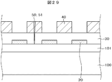
図28は、図27のF-F断面図である。図28において、第2有機パッシベーション膜40は端子配線20の上には形成されておらず、端子配線20の存在しないところに形成されている。例えば、第2有機パッシベーション膜40の間隔prは0.1mm程度であり、端子配線20の間隔が、間隔prの半分の0.05mmで形成される。すなわち、端子配線20の配線間に有機パッシベーション膜40を形成することができる。
ハンドリング等による傷51あるいはクラック50は、殆どが第2有機パッシベーション膜40の表面に生ずる。この様子を図29に示す。図29に示すように、第2有機パッシベーション膜40の表面に傷51あるいはクラック50が生じ、それらが伝搬したとしても、この部分には、端子配線20が存在しないために、端子配線20が直接影響を受け、断線をするということは無い。
なお、第2有機パッシベーション膜40と端子配線20との間に、平面で視て、多少の重複が生じても、あるいは、多少の隙間が生じても、作用効果に大きな差は生じない。
実施例1乃至4では、有機EL表示装置について本発明を説明した。しかし、本発明は、液晶表示装置や、指紋や静脈、触覚等を2次元的にセンシングするセンサ装置でも、フレキシブル基板を用いる場合は、同様に適用することが出来る。
11…走査線、 12…映像信号線、 13…電源線、 14…画素、 18…走査線駆動回路、 20…端子配線、 30…第1有機パッシベーション膜、 40…第2有機パッシベーション膜、 50…クラック、 51…傷、 60…SiN膜、 90…表示領域、 95…端子領域、 100…TFT基板、 101…有機下地膜、 102…無機下地膜、 103…半導体層、 104…接続電極、 105…ゲート絶縁膜、 106…ゲート電極、 107…層間絶縁膜、 108…ドレイン電極、 109…ソース電極、 110…有機パッシベーション膜、 111…下部電極、 112…バンク、 113…有機EL層、 114…上部電極、 115…保護膜、 116…粘着材、 117…円偏光板、 1101…スルーホール、 1121…ホール、 BA…曲げ領域、 M…中立面
Claims (16)
- 湾曲可能な基板に表示領域と端子領域が形成されたフレキシブルパネル装置であって、
前記端子領域は他の配線基板と接続する端部を有し、
前記端子領域には、端子配線が、前記表示領域から前記端部に向かう第1の方向に延在し、かつ、前記第1の方向と交差する方向である第2の方向に複数配列し、
前記端子配線を覆って第1有機パッシベーション膜が形成され、前記第1有機パッシベーション膜の上には、第2有機パッシベーション膜が形成され、
前記第2有機パッシベーション膜は、前記第1の方向に延在し、前記第2の方向に複数配列するように形成されていることを特徴とするフレキシブルパネル装置。 - 前記第2有機パッシベーション膜は、平面で視て、前記端子配線を覆うように形成されていることを特徴とする請求項1に記載のフレキシブルパネル装置。
- 複数の前記第2有機パッシベーション膜の前記第2の方向の間隔は、複数の前記端子配線の前記第2の方向の間隔と同じであることを特徴とする請求項1に記載のフレキシブルパネル装置。
- 前記第2有機パッシベーション膜の前記第2の方向の幅は、前記端子配線の前記第2の方向の幅よりも大きいことを特徴とする請求項1に記載のフレキシブルパネル装置。
- 前記第2有機パッシベーション膜は、平面で視て、前記端子配線間の前記第2の方向の間隔と重複するように配置されていることを特徴とする請求項1に記載のフレキシブルパネル装置。
- 前記第2有機パッシベーション膜の前記第2の方向の幅は、平面で視て、前記端子配線間の前記第2の方向の間隔よりも大きいことを特徴とする請求項5に記載のフレキシブルパネル装置。
- 前記第2有機パッシベーション膜はポリイミドで形成されていることを特徴とする請求項1に記載のフレキシブルパネル装置。
- 前記第1有機パッシベーション膜はポリイミドで形成されていることを特徴とする請求項1に記載のフレキシブルパネル装置。
- 前記フレキシブルパネル装置は有機EL表示装置であることを特徴とする請求項1に記載のフレキシブルパネル装置。
- 前記フレキシブルパネル装置は液晶表示装置であることを特徴とする請求項1に記載のフレキシブルパネル装置。
- 湾曲可能な基板に表示領域と端子領域が形成されたフレキシブルパネル装置であって、
前記端子領域は他の配線基板と接続する端部を有し、
前記端子領域には、端子配線が、前記表示領域から前記端部に向かう第1の方向にジグザグ状に延在し、かつ、前記第1の方向と交差する方向の第2の方向に複数配列し、
前記端子配線を覆って第1有機パッシベーション膜が形成され、前記第1有機パッシベーション膜の上には、第2有機パッシベーション膜が形成され、
前記第2有機パッシベーション膜は、平面で視て、前記第1の方向にジグザグ状に延在し、前記第2の方向に複数配列するように形成されていることを特徴とするフレキシブルパネル装置。 - 前記第2有機パッシベーション膜は、平面で視て、前記端子配線を覆うように形成されていることを特徴とする請求項11に記載のフレキシブルパネル装置。
- 前記第2有機パッシベーション膜の前記第2方向の幅は、前記端子配線の前記第2の方向の幅よりも大きいことを特徴とする請求項12に記載のフレキシブルパネル装置。
- 前記第2有機パッシベーション膜は、平面で視て、前記端子配線間の前記第2の方向の間隔と重複するように形成されていることを特徴とする請求項11に記載のフレキシブルパネル装置。
- 湾曲可能な基板に表示領域と端子領域が形成されたフレキシブルパネル装置であって、
前記端子領域は他の配線基板と接続する端部を有し、
前記端子領域には、端子配線が前記表示領域から前記端部に向かう第1の方向にジグザグ状に延在し、かつ、前記第1の方向と交差する方向の第2の方向に複数配列し、
前記端子配線を覆って第1有機パッシベーション膜が形成され、前記第1有機パッシベーション膜の上には、第2有機パッシベーション膜が形成され、
前記第2の有機パッシベーション膜は、前記ジグザク状に形成された端子配線の屈曲部と重畳する位置に、前記第2の方向に延在し、前記第1の方向に複数配列されていることを特徴とするフレキシブルパネル装置。 - 前記第2の有機パッシベーション膜は、前記第2の方向に直線状に延在し、前記第1の方向に複数平行に配列していることを特徴とする請求項15に記載のフレキシブルパネル装置。
Applications Claiming Priority (2)
| Application Number | Priority Date | Filing Date | Title |
|---|---|---|---|
| JP2019060267A JP2020160305A (ja) | 2019-03-27 | 2019-03-27 | フレキシブルパネル装置 |
| JP2019-060267 | 2019-03-27 |
Publications (1)
| Publication Number | Publication Date |
|---|---|
| WO2020196085A1 true WO2020196085A1 (ja) | 2020-10-01 |
Family
ID=72611494
Family Applications (1)
| Application Number | Title | Priority Date | Filing Date |
|---|---|---|---|
| PCT/JP2020/011665 Ceased WO2020196085A1 (ja) | 2019-03-27 | 2020-03-17 | フレキシブルパネル装置 |
Country Status (2)
| Country | Link |
|---|---|
| JP (1) | JP2020160305A (ja) |
| WO (1) | WO2020196085A1 (ja) |
Families Citing this family (41)
| Publication number | Priority date | Publication date | Assignee | Title |
|---|---|---|---|---|
| TW202240886A (zh) | 2020-12-04 | 2022-10-16 | 日商半導體能源研究所股份有限公司 | 顯示面板、資料處理裝置及用於製造顯示面板之方法 |
| KR20230110579A (ko) | 2020-12-04 | 2023-07-24 | 가부시키가이샤 한도오따이 에네루기 켄큐쇼 | 표시 장치, 표시 모듈, 및 표시 장치의 제작 방법 |
| KR20230112706A (ko) | 2020-12-06 | 2023-07-27 | 가부시키가이샤 한도오따이 에네루기 켄큐쇼 | 표시 장치 및 표시 보정 시스템 |
| JP7797414B2 (ja) | 2020-12-07 | 2026-01-13 | 株式会社半導体エネルギー研究所 | 表示装置 |
| WO2022123382A1 (ja) | 2020-12-07 | 2022-06-16 | 株式会社半導体エネルギー研究所 | 表示装置の作製方法、表示装置、表示モジュール、及び、電子機器 |
| WO2022137013A1 (ja) | 2020-12-25 | 2022-06-30 | 株式会社半導体エネルギー研究所 | 表示装置、電子機器、及び表示装置の作製方法 |
| WO2022144661A1 (ja) | 2020-12-29 | 2022-07-07 | 株式会社半導体エネルギー研究所 | 表示パネル、情報処理装置、表示パネルの製造方法 |
| CN116670743A (zh) | 2020-12-29 | 2023-08-29 | 株式会社半导体能源研究所 | 显示装置的制造方法 |
| DE102021134032A1 (de) | 2020-12-29 | 2022-06-30 | Semiconductor Energy Laboratory Co., Ltd. | Licht emittierende Vorrichtung, Licht emittierende Einrichtung, elektronisches Gerät und Beleuchtungsvorrichtung |
| JP7824892B2 (ja) | 2021-01-14 | 2026-03-05 | 株式会社半導体エネルギー研究所 | 表示装置 |
| KR20230129184A (ko) | 2021-01-14 | 2023-09-06 | 가부시키가이샤 한도오따이 에네루기 켄큐쇼 | 표시 장치의 제작 방법, 표시 장치, 표시 모듈, 및전자 기기 |
| JPWO2022153150A1 (ja) | 2021-01-14 | 2022-07-21 | ||
| TW202232796A (zh) | 2021-01-14 | 2022-08-16 | 日商半導體能源研究所股份有限公司 | 顯示裝置 |
| JP2022115080A (ja) | 2021-01-27 | 2022-08-08 | 株式会社半導体エネルギー研究所 | 表示装置 |
| US12527167B2 (en) | 2021-01-28 | 2026-01-13 | Semiconductor Energy Laboratory Co., Ltd. | Display device |
| US12532606B2 (en) | 2021-01-28 | 2026-01-20 | Semiconductor Energy Laboratory Co., Ltd. | Method for manufacturing display device, display device, display module, and electronic device |
| JPWO2022175789A1 (ja) | 2021-02-19 | 2022-08-25 | ||
| WO2022180480A1 (ja) | 2021-02-25 | 2022-09-01 | 株式会社半導体エネルギー研究所 | 半導体装置、及び電子機器 |
| DE112022001242T5 (de) | 2021-02-26 | 2023-12-21 | Semiconductor Energy Laboratory Co., Ltd. | Anzeigevorrichtung und elektronisches Gerät |
| US12601045B2 (en) | 2021-03-25 | 2026-04-14 | Semiconductor Energy Laboratory Co., Ltd. | Manufacturing equipment for light-emitting device |
| US12349538B2 (en) | 2021-03-25 | 2025-07-01 | Semiconductor Energy Laboratory Co., Ltd. | Light-emitting device, display device, light-emitting apparatus, electronic device, and lighting device |
| US12477918B2 (en) | 2021-03-31 | 2025-11-18 | Semiconductor Energy Laboratory Co., Ltd. | Display apparatus, display module, electronic device, and method for manufacturing display apparatus |
| US12245485B2 (en) | 2021-04-08 | 2025-03-04 | Semiconductor Energy Laboratory Co., Ltd. | Display apparatus including light-emitting device and light-receiving device |
| JP7851915B2 (ja) | 2021-04-22 | 2026-04-27 | 株式会社半導体エネルギー研究所 | 表示装置 |
| CN117178314A (zh) | 2021-04-22 | 2023-12-05 | 株式会社半导体能源研究所 | 显示装置及显示装置的制造方法 |
| US11815689B2 (en) | 2021-04-30 | 2023-11-14 | Semiconductor Energy Laboratory Co., Ltd. | Electronic device |
| US11699391B2 (en) | 2021-05-13 | 2023-07-11 | Semiconductor Energy Laboratory Co., Ltd. | Semiconductor device, display apparatus, and electronic device |
| US12527192B2 (en) | 2021-05-13 | 2026-01-13 | Semiconductor Energy Laboratory Co., Ltd. | Display apparatus, display module, electronic device, and method for manufacturing display apparatus |
| US12426474B2 (en) | 2021-05-27 | 2025-09-23 | Semiconductor Energy Laboratory Co., Ltd. | Display apparatus, method for manufacturing display apparatus, display module, and electronic device |
| US12506126B2 (en) | 2021-06-17 | 2025-12-23 | Semiconductor Energy Laboratory Co., Ltd. | Display device |
| TW202306210A (zh) | 2021-06-25 | 2023-02-01 | 日商半導體能源研究所股份有限公司 | 受光器件、受發光裝置 |
| KR20230000968A (ko) | 2021-06-25 | 2023-01-03 | 가부시키가이샤 한도오따이 에네루기 켄큐쇼 | 발광 디바이스, 표시 장치, 발광 장치, 전자 기기, 및 조명 장치 |
| KR20230004278A (ko) | 2021-06-30 | 2023-01-06 | 가부시키가이샤 한도오따이 에네루기 켄큐쇼 | 발광 디바이스 및 발광 장치 |
| US12262623B2 (en) | 2021-06-30 | 2025-03-25 | Semiconductor Energy Laboratory Co., Ltd. | Manufacturing method of display device |
| US12604662B2 (en) | 2021-07-16 | 2026-04-14 | Semiconductor Energy Laboratory Co., Ltd. | Light-emitting device and light-emitting apparatus |
| JPWO2023031718A1 (ja) | 2021-08-31 | 2023-03-09 | ||
| KR20240093546A (ko) | 2021-10-27 | 2024-06-24 | 가부시키가이샤 한도오따이 에네루기 켄큐쇼 | 표시 장치 |
| CN118355431A (zh) | 2021-12-08 | 2024-07-16 | 株式会社半导体能源研究所 | 电子设备 |
| US12604650B2 (en) | 2021-12-20 | 2026-04-14 | Semiconductor Energy Laboratory Co., Ltd. | Method for manufacturing light-emitting element and light-emitting device using photolithography technique |
| CN118661127A (zh) | 2022-02-09 | 2024-09-17 | 株式会社半导体能源研究所 | 电子设备 |
| US12598869B2 (en) | 2022-03-25 | 2026-04-07 | Semiconductor Energy Laboratory Co., Ltd. | Imaging device, display apparatus, and method for manufacturing display apparatus |
Citations (7)
| Publication number | Priority date | Publication date | Assignee | Title |
|---|---|---|---|---|
| US20140232956A1 (en) * | 2013-02-15 | 2014-08-21 | Lg Display Co., Ltd. | Flexible organic light emitting display device and method for manucaturing the same |
| US20170301272A1 (en) * | 2016-04-18 | 2017-10-19 | Samsung Display Co., Ltd. | Display device and method of testing the same |
| JP2017227830A (ja) * | 2016-06-24 | 2017-12-28 | 株式会社ジャパンディスプレイ | 表示装置 |
| US20180040838A1 (en) * | 2017-04-27 | 2018-02-08 | Shanghai Tianma Micro-electronics Co., Ltd. | Flexible display screen and flexible display device |
| JP2018054675A (ja) * | 2016-09-26 | 2018-04-05 | 株式会社ジャパンディスプレイ | 表示装置 |
| US20180123060A1 (en) * | 2016-10-31 | 2018-05-03 | Lg Display Co., Ltd. | Organic light emitting display device and method of manufacturing the same |
| JP2018124503A (ja) * | 2017-02-03 | 2018-08-09 | 株式会社ジャパンディスプレイ | 表示装置 |
-
2019
- 2019-03-27 JP JP2019060267A patent/JP2020160305A/ja active Pending
-
2020
- 2020-03-17 WO PCT/JP2020/011665 patent/WO2020196085A1/ja not_active Ceased
Patent Citations (7)
| Publication number | Priority date | Publication date | Assignee | Title |
|---|---|---|---|---|
| US20140232956A1 (en) * | 2013-02-15 | 2014-08-21 | Lg Display Co., Ltd. | Flexible organic light emitting display device and method for manucaturing the same |
| US20170301272A1 (en) * | 2016-04-18 | 2017-10-19 | Samsung Display Co., Ltd. | Display device and method of testing the same |
| JP2017227830A (ja) * | 2016-06-24 | 2017-12-28 | 株式会社ジャパンディスプレイ | 表示装置 |
| JP2018054675A (ja) * | 2016-09-26 | 2018-04-05 | 株式会社ジャパンディスプレイ | 表示装置 |
| US20180123060A1 (en) * | 2016-10-31 | 2018-05-03 | Lg Display Co., Ltd. | Organic light emitting display device and method of manufacturing the same |
| JP2018124503A (ja) * | 2017-02-03 | 2018-08-09 | 株式会社ジャパンディスプレイ | 表示装置 |
| US20180040838A1 (en) * | 2017-04-27 | 2018-02-08 | Shanghai Tianma Micro-electronics Co., Ltd. | Flexible display screen and flexible display device |
Also Published As
| Publication number | Publication date |
|---|---|
| JP2020160305A (ja) | 2020-10-01 |
Similar Documents
| Publication | Publication Date | Title |
|---|---|---|
| WO2020196085A1 (ja) | フレキシブルパネル装置 | |
| US11825713B2 (en) | Display device | |
| US20240268170A1 (en) | Display device | |
| US11699706B2 (en) | Display device | |
| CN107887416B (zh) | 背板基板和使用该背板基板的柔性显示器 | |
| US11003036B2 (en) | Pixel array substrate | |
| CN105074802B (zh) | 具有柔性显示器的电子装置 | |
| US20190140202A1 (en) | Flexible display panel and flexible display apparatus | |
| US20190157311A1 (en) | Flexible array substrate and preparation method thereof, display substrate and display device | |
| US10181504B2 (en) | Flexible display panel with redundant bent signal lines | |
| TWI512375B (zh) | 液晶顯示裝置 | |
| TWI553838B (zh) | 畫素陣列基板與面板 | |
| CN107845643A (zh) | 一种显示面板及显示装置 | |
| CN103677406B (zh) | 触控面板与触控显示面板 | |
| EP4020578B1 (en) | Display device and method of manufacturing the same | |
| CN102902084A (zh) | 扇出信号线区的结构及显示面板 | |
| TWI406033B (zh) | 一種陣列基板的扇出線路 | |
| CN107193167A (zh) | 阵列基板及液晶显示面板 | |
| JP2018077983A (ja) | 表示装置 | |
| CN112631448A (zh) | 触控显示面板 |
Legal Events
| Date | Code | Title | Description |
|---|---|---|---|
| 121 | Ep: the epo has been informed by wipo that ep was designated in this application |
Ref document number: 20778792 Country of ref document: EP Kind code of ref document: A1 |
|
| NENP | Non-entry into the national phase |
Ref country code: DE |
|
| 122 | Ep: pct application non-entry in european phase |
Ref document number: 20778792 Country of ref document: EP Kind code of ref document: A1 |