WO2020195460A1 - 感圧部材及び圧力検出装置 - Google Patents
感圧部材及び圧力検出装置 Download PDFInfo
- Publication number
- WO2020195460A1 WO2020195460A1 PCT/JP2020/007488 JP2020007488W WO2020195460A1 WO 2020195460 A1 WO2020195460 A1 WO 2020195460A1 JP 2020007488 W JP2020007488 W JP 2020007488W WO 2020195460 A1 WO2020195460 A1 WO 2020195460A1
- Authority
- WO
- WIPO (PCT)
- Prior art keywords
- pressure
- sensitive
- electrodes
- base material
- conductive member
- Prior art date
- Legal status (The legal status is an assumption and is not a legal conclusion. Google has not performed a legal analysis and makes no representation as to the accuracy of the status listed.)
- Ceased
Links
Images





Classifications
-
- G—PHYSICS
- G01—MEASURING; TESTING
- G01L—MEASURING FORCE, STRESS, TORQUE, WORK, MECHANICAL POWER, MECHANICAL EFFICIENCY, OR FLUID PRESSURE
- G01L1/00—Measuring force or stress, in general
- G01L1/20—Measuring force or stress, in general by measuring variations in ohmic resistance of solid materials or of electrically-conductive fluids; by making use of electrokinetic cells, i.e. liquid-containing cells wherein an electrical potential is produced or varied upon the application of stress
Definitions
- the present invention relates to a pressure sensitive member and a pressure detecting device.
- a detection device including a resistance change detection type pressure sensitive member whose resistance value (electrical resistance value) changes when a pressing force is applied is widely known. Since such a detection device has a simple configuration and a good feel when touched, application to a touch panel of an electronic device such as a tactile sensor of a robot or a mobile information terminal is being studied as a pressure sensor. ..
- Patent Document 1 discloses a detection device in which an elastic substrate, a pressure-sensitive conductive sheet, a pair of electrodes, and a rigid substrate are laminated in this order from the side on which an external force acts.
- the elastic substrate is a substrate having elasticity that is deformed by the action of an external force and recovers to the original shape when the external force is unloaded.
- a non-conductive elastomer such as silicon rubber. It is made of resin or the like.
- the pressure-sensitive conductive sheet a conductor formed by dispersing conductive particles such as carbon particles in a non-conductive elastomer resin and deformed by an external force is used.
- One aspect of the present invention is to provide a pressure sensitive member capable of stably detecting a pressing force applied from the outside with high sensitivity.
- One aspect of the pressure-sensitive member according to the present invention is an elastic base material that has an action surface on which a pressing force acts and is elastically deformable by the pressing force, and a transmission surface of the elastic base material on the side opposite to the acting surface.
- the pressure-sensitive conductive member is provided with a pair of electrodes and a pressure-sensitive conductive member provided on the transmission surface so as to be electrically connectable to the pair of electrodes, and the pressure-sensitive conductive member changes the pressing force. Due to the elastic deformation, the electric resistance value between the pair of electrodes changes.
- One aspect of the pressure-sensitive member according to the present invention can stably detect a pressing force applied from the outside with high sensitivity.
- FIG. 1 is a cross-sectional view taken along the line II of FIG. It is explanatory drawing which shows the change of the resistance value of a pressure-sensitive conductive member. It is explanatory drawing which shows an example of the state which a pressure sensitive member is pressed. It is explanatory drawing which shows an example of the state which the pressure-sensitive member which arranged the electrode under the pressure-sensitive conductive member is pressed. It is a perspective view of the pressure detection device which applied the pressure sensitive member.
- FIG. 7 is a sectional view taken along line II-II of FIG. It is a figure explaining the indentation test. It is a figure which shows the relationship between the pressure and resistance of Example 1, Comparative Example 1 and 2. It is a figure which shows the relationship between the pressure and resistance of the comparative example 3.
- each member in the drawing may differ from the actual scale.
- a three-dimensional Cartesian coordinate system in three axial directions (X-axis direction, Y-axis direction, Z-axis direction) is used, the length direction of the sensitive member is the X-axis direction, and the width direction of the pressure-sensitive member is the Y-axis.
- the direction is defined as the height direction of the pressure sensitive member in the Z-axis direction.
- the elastic base material side of the pressure sensitive member is the + Z axis direction, and the opposite direction is the ⁇ Z axis direction.
- the + Z-axis direction may be referred to as up
- the ⁇ Z-axis direction may be referred to as down.
- the tilde "-" indicating a numerical range in the present specification means that the numerical values described before and after the tilde are included as the lower limit value and the upper limit value.
- FIG. 1 is a perspective view showing an example of the configuration of the pressure-sensitive member according to the embodiment
- FIG. 2 is an exploded perspective view of the pressure-sensitive member according to the embodiment
- FIG. 3 is FIG. 1II. It is a cross-sectional view.
- the pressure-sensitive member 10 includes an elastic base material 11, an adhesive layer 12, a pair of electrodes 13A and 13B, an adhesive layer 14, a pressure-sensitive conductive member 15, and a rigid group.
- the material 16 is provided, and the electrode 13A and the electrode 13B are electrically connected.
- each member constituting the pressure sensitive member 10 will be described.
- the elastic base material 11 is a plate-shaped member that is formed in a rectangular shape in a plan view and can be elastically deformed by a pressing force.
- the elastic base material 11 is a substrate having elasticity that is deformed by the action of the pressing force and recovers to the original shape when the pressing force is released.
- the elastic base material 11 has a pair of main surfaces parallel to each other, the main surface on which the pressing force acts is the acting surface 111, and the main surface opposite to the acting surface 111 is the transmission surface 112 that transmits the pressing force. is there.
- the elastic base material 11 can be formed by using an elastomer or a synthetic resin.
- the material for forming the elastomer include natural rubber, silicone rubber, chloroprene rubber, isoprene rubber, butyl rubber, acrylic rubber, nitrile rubber, urethane rubber, polyisobutylene rubber, butadiene rubber, styrene-butadiene rubber, and ethylene-propylene rubber. Chlorosulfonated polyethylene rubber, epichlorohydrin rubber, polyester rubber, fluororubber, and modified products thereof can be used.
- the synthetic resin a flexible epoxy resin or the like can be used. These may be used individually by 1 type, and may be used in combination of 2 or more type.
- silicone rubber is preferable.
- the elastic base material 11 has high elasticity and can have good adhesion to the adhesive layer 12. Further, since the elastic base material 11 is deformed at the point of action of the pressing force and can receive the pressing force without moving the point of action, the pressing force is transferred from the transmission surface 112 to the electrodes 13A and 13B. It is accurately transmitted to the pressure-sensitive conductive member 15.
- the thickness of the elastic base material 11 is preferably 10 ⁇ m to 100 ⁇ m, more preferably 20 ⁇ m to 75 ⁇ m, and even more preferably 25 ⁇ m to 50 ⁇ m. When the thickness of the elastic base material 11 is in the range of 10 ⁇ m to 100 ⁇ m, the elastic base material 11 has sufficient strength and can have elasticity.
- the adhesive layer 12 is provided on the transmission surface 112 on the side opposite to the working surface 111 of the elastic base material 11, and is provided between the elastic base material 11 and the electrodes 13A and 13B.
- the adhesive layer 12 has a function of increasing the adhesive force between the elastic base material 11 and the electrodes 13A and 13B, and fixes the electrodes 13A and 13B.
- a triazine thiol compound can be used.
- a triazine thiol compound for example, a triazine ring having a thiol group (-SH group) or an alkali metal salt of a thiol group can be used. Any one of the functional groups may have another structure such as a dibutylamino group or an anirino group.
- Specific examples of the triazinethiol compound include 6- (3-triethoxysilylpropylamino) -1,3,5-triazine-2,4-dithiol and 2,6-diazide-4- ⁇ 3- (tri).
- sodium salts examples include 2,4,6-trimercapto-1,3,5-triazine monosodium salt and the like. These may be used alone or in combination of two or more. In addition, 1,3,5-triazine is also referred to as s-triazine.
- the thickness of the adhesive layer 12 is about 1 nm to 100 nm.
- the adhesive layer 12 may be formed by using a general adhesive. In this case, the thickness of the adhesive layer 12 is preferably 1 ⁇ m to 20 ⁇ m, more preferably 3 ⁇ m to 15 ⁇ m, and even more preferably 5 ⁇ m to 10 ⁇ m.
- the pair of electrodes 13A and 13B are provided on the transmission surface 112 of the elastic base material 11 via the adhesive layer 12.
- the electrodes 13A and 13B are provided so as to face each other in a state of being insulated from each other, and have a comb tooth electrode having a tip formed in a comb tooth shape.
- the electrodes 13A and 13B are terminals to which the main body portions 131A and 131B formed linearly in the X-axis direction, the tip portions 132A and 132B (comb tooth electrodes) formed in a comb shape, and the external wiring are connected. It has parts 133A and 133B.
- the terminal portions 133A and 133B are formed in a rectangular shape and are provided at the positions of the ends of the elastic base material 11 on the ⁇ X axis direction side in a plan view.
- the adhesive layer 14 is not coated on the terminal portions 133A and 133B. Further, in the present embodiment, as shown in FIG. 3, the rigid base material 16 is not arranged so as to face each other.
- the electrodes 13A and 13B may be composed of a composite film in which the material forming the electrodes 13A and 13B is used as a conductive member and dispersed in a binder such as a synthetic resin. At that time, when a synthetic resin is used as the binder, it is preferable to use an elastomer similar to that of the elastic base material 11. As a result, the electrodes 13A and 13B having the tip portions 132A and 132B that easily follow the local deformation of the elastic base material 11 can be obtained.
- the thickness of the adhesive layer 14 can be appropriately designed and is preferably 0.08 mm to 0.12 mm. When the thickness of the pressure-sensitive adhesive layer 14 is within the range of 0.05 mm to 0.20 mm, the pressure-sensitive adhesive layer 14 has sufficient adhesive strength and can suppress the thickness of the pressure-sensitive member 10.
- the thickness of the pressure-sensitive conductive member 15 is preferably 0.1 mm to 10 mm, more preferably 0.5 mm to 5 mm, and even more preferably 0.7 mm to 3 mm. When the thickness of the pressure-sensitive conductive member 15 is within the range of 0.1 mm to 10 mm, the pressure-sensitive conductive member 15 can have sufficient strength and elasticity.
- Examples of the material for forming the rigid base material 16 include polyamide (PA), polyimide (PI), polybutylene terephthalate (PET), polyethylene naphthalate (PEN), polyetherimide (PEI), and polyethersulfone (PES).
- Synthetic resins such as polystyrene (PS), polymethylmethacrylate (PMMA), polyethylenenitrile, polyetheretherketone (PEEk), polyphenylene sulfide (PPS), phenol, epoxy (with glass filler) and polycarbonate (PC) can be used. It can. These may be used alone or in combination of two or more. Among these, it is preferable to use polyimide, polyethylene terephthalate, or the like from the viewpoint of heat resistance and the like.
- the thickness of the rigid base material 16 can be appropriately designed and depends on the type of material, but if it is a synthetic resin material having low rigidity, it is preferably 0.5 mm to 1.5 mm, and a metal having high rigidity. If it is a material, it is preferably 0.1 mm to 0.5 mm. Within this range, the rigid base material 16 can have sufficient strength.
- An elastic base material 11 cut out to a predetermined size in a plan view is prepared.
- the surface of the prepared elastic base material 11 is washed with a cleaning liquid such as water, alcohol, or acetone to remove dirt, foreign substances, and the like adhering to the surface of the elastic base material 11.
- a molecular adhesive containing a triazine compound is applied to the transmission surface 112 of the elastic base material 11 and dried to form the adhesive layer 12.
- a coating liquid (paste) containing a conductive material such as Ag particles and Cu particles is applied to the surface of the adhesive layer 12 to form electrodes 13A and 13B.
- the electrodes 13A and 13B are fixed by the adhesive layer 12.
- a metal plating film is formed by a method using electroless plating, electroplating, sputtering, or vapor deposition. A method of forming the above may be used.
- the pressure-sensitive conductive member 15 is installed on the surfaces of the tips 132A and 132B of the electrodes 13A and 13B, a part of the electrodes 13A and 13B and the pressure-sensitive conductive member 15 are placed on the transmission surface 112.
- the adhesive layer 14 is provided so as to cover and.
- the rigid base material 16 is installed on the surface of the adhesive layer 14, and the adhesive layer 14 is sandwiched between the elastic base material 11 and the rigid base material 16.
- the pressure sensitive member 10 according to the present embodiment can be obtained.
- the electrodes 13A and 13B and the conductive material 151 are hardly in contact with each other, and the electrodes 13A and 13B are almost in contact with each other. Since it is not conducting, the pressure-sensitive conductive member 15 has a high resistance value.
- the formed conduction path becomes three-dimensionally larger or smaller, so that the pressing force can be detected by the resistance value.
- the pressing force acting on the pressure-sensitive conductive member 15 is attenuated and becomes smaller, so that the conductive materials 151 in the pressure-sensitive conductive member 15 are separated from each other. There is almost no change in the distance between the conductive materials 151 before the pressing force is applied. Alternatively, a small tensile stress is generated on the lower surface of the pressure-sensitive conductive member 15, and the distance between the conductive materials 151 tends to increase. Therefore, on the lower surface side of the pressure-sensitive conductive member 15, a conduction path is hardly formed in the pressure-sensitive conductive member 15.
- the action surface 111 of the elastic base material 11 is as shown in FIG.
- the pressing force acting on the pressure-sensitive conductive member 15 the pressing force applied to the acting surface 111 can be applied to the pressure-sensitive conductive member 15 from the transmission surface 112 before the pressing force is attenuated.
- the pressing force acting on the pressure-sensitive conductive member 15 deforms the electrodes 13A and 13B of the pressure-sensitive conductive member 15 so as to crush the vicinity regions on the installation surface side, so that the electrodes of the pressure-sensitive conductive member 15 are crushed.
- the pressure-sensitive member 10 maintains the pressing force applied to the working surface 111 of the elastic base material 11 as much as possible on the installation surface side of the electrodes 13A and 13B of the pressure-sensitive conductive member 15. Since it can be transmitted in the state of being pressed, it is possible to increase the detection sensitivity and suppress the variation in the magnitude of the pressing force. Therefore, the pressure-sensitive member 10 can stably detect the pressing force applied from the outside with high sensitivity.
- the electrodes 13A and 13B are provided between the elastic base material 11 and the pressure-sensitive conductive member 15, so that the thickness of the pressure-sensitive conductive member 15 becomes the working surface 111 of the elastic base material 11. It can be transmitted to the electrodes 13A and 13B without reducing the magnitude of the applied pressing force. Therefore, since the pressure-sensitive member 10 can increase the thickness of the pressure-sensitive conductive member 15, the range in which the pressing force can be received can be expanded.
- the pressure-sensitive member 10 can stably detect the pressing force applied from the outside with high sensitivity, and can have a simple structure and a good feel when touched. Therefore, the pressure-sensitive member 10 can be suitably used as a pressure detection device (pressure-sensitive sensor) for a tactile sensor of a robot, a touch panel of an electronic device, or the like.
- a pressure detection device pressure-sensitive sensor
- electronic devices include devices equipped with touch panels such as information mobile terminals, mobile phones, personal computers, digital cameras, video cameras, car navigation systems, electronic organizers, calculators, and videophones.
- the connecting portion 31 sandwiches the elastic base material 11 of the pressure-sensitive member 10, the adhesive layer 12, and one end portions (-Y-axis direction) of the electrodes 13A and 13B, and is electrically connectably connected to the electrodes 13A and 13B. ing.
- the connection unit 31 has a function of flowing a current flowing through the electrodes 13A and 13B to the detection unit 32 via the wiring 34 while connecting to the electrodes 13A and 13B, respectively.
- the elastic base material 11 of the pressure sensitive member 10 When the elastic base material 11 of the pressure sensitive member 10 is pressed and a current change (change in resistance value) occurs in the electrodes 13A and 13B, the current between the electrodes 13A and 13B is detected via the connection portion 31 and the wiring 34. The process of being sent to the unit 32 and converted into an electric signal is performed. Then, the pressure value is calculated by detecting the change in the resistance value of the pressure sensitive member 10.
- the pressure detecting device 30 includes the pressure sensitive member 10, when the pressure sensitive member 10 is pressed, the pressing pressure can be stably detected with high sensitivity.
- the pressure-sensitive member 10 does not have to include the adhesive layer 12 when the electrodes 13A and 13B can be fixed to the transmission surface 112 even if the adhesive layer 12 is not particularly provided.
- the adhesive layer 12 may be formed on at least a part of the transmission surface 112 in contact with the electrodes 13A and 13B as long as the electrodes 13A and 13B can be fixed.
- An elastic base material 11 (see FIG. 1) cut out to a predetermined size from silicone rubber (“ultra-thin SR sheet”, manufactured by AS ONE Corporation, thickness 0.1 mm) was prepared.
- the prepared elastic base material 11 is immersed in an ethanol solution, washed for 30 seconds, subjected to corona discharge for 20 seconds, and then a molecular adhesive is applied to one main surface of the elastic base material 11 and dried.
- An adhesive layer 12 (see FIG. 3) was formed. After that, Ag ink (“SSP2801”, manufactured by Toyobo Co., Ltd.) is applied to the surface of the adhesive layer 12, and as shown in FIG.
- a pair of electrodes 13A and 13B arranged so that the tips have a comb-like shape. was formed.
- the pressure-sensitive conductive member 15 is arranged at the tip portions of the pair of electrodes 13A and 13B, and a double-sided adhesive tape (“No.7082”, manufactured by Teraoka Seisakusho Co., Ltd.) is attached as the adhesive layer 14 to the double-sided adhesive tape.
- Comparative Examples 1 to 3 In Comparative Examples 1 to 3, the same method as in Example 1 was performed except that a known pressure-sensitive member was used as the pressure-sensitive member.
- a known pressure-sensitive member a pressure-sensitive member in which a pressure-sensitive conductive member and an adhesive layer are laminated on a rigid substrate on which a pair of electrodes are formed, and an elastic substrate is further laminated is used.
- the difference between the pressure-sensitive member 10 of Example 1 and the pressure-sensitive members of Comparative Examples 1 to 3 is that the positions where the pair of electrodes are formed are different.
- the pressure-sensitive member of one embodiment can detect a small pressing force with high sensitivity and stability at an early stage.
Landscapes
- Physics & Mathematics (AREA)
- General Physics & Mathematics (AREA)
- Force Measurement Appropriate To Specific Purposes (AREA)
- Push-Button Switches (AREA)
Abstract
本発明に係る感圧部材は、押圧力の作用する作用面を有し、前記押圧力で弾性変形可能な弾性基材と、前記弾性基材の前記作用面と反対側の伝達面に設けられた、一対の電極と、前記一対の電極と電気的に接続可能に前記伝達面に設けられた感圧導電性部材と、を備え、前記感圧導電性部材が前記押圧力の変化により弾性変形し、前記一対の電極間の電気抵抗値が変化する。
Description
本発明は、感圧部材及び圧力検出装置に関する。
押圧力が加えられることにより抵抗値(電気抵抗値)が変化する抵抗変化検出型の感圧部材等を備える検出装置が広く知られている。このような検出装置は、構成が簡便であり、触れた時の感触も良いため、感圧センサとして、ロボットの触覚センサや携帯情報端末等の電子機器のタッチパネル等への応用が検討されている。
このような抵抗変化検出型の感圧部材として、感圧性の導電ゴムの裏面に電極を形成した検出装置がある(例えば、特許文献1参照)。特許文献1には、弾性基板と、感圧導電シートと、一対の電極と、剛性基板とを、外力が作用する側からこの順に積層された検出装置が開示されている。
特許文献1の検出装置では、弾性基板は、外力が作用することによって変形し、外力が除荷されると元の形状に回復する弾性を有する基板であり、例えばシリコンゴム等の非導電性エラストマー樹脂等で形成されている。感圧導電シートとしては、非導電性エラストマー樹脂に、炭素粒子などの導電性粒子を分散させて形成され、外力によって変形する導電体が用いられている。
しかしながら、特許文献1の検出装置は、外力が直接作用する弾性基板を非導電性エラストマー樹脂等で形成し、弾性基板と一対の電極との間に感圧導電シートを配置している。そのため、弾性基板に加わる外力が一対の電極に対してダイレクトに伝わり難い。よって、特許文献1の検出装置では、外力に対する感度を高くできず、外力を安定して検出できなかった。
本発明の一態様は、外部から加わる押圧力を高感度で安定して検出することができる感圧部材を提供することを目的とする。
本発明に係る感圧部材の一態様は、押圧力の作用する作用面を有し、前記押圧力で弾性変形可能な弾性基材と、前記弾性基材の前記作用面と反対側の伝達面に設けられた、一対の電極と、前記一対の電極と電気的に接続可能に前記伝達面に設けられた感圧導電性部材と、を備え、前記感圧導電性部材が前記押圧力の変化により弾性変形し、前記一対の電極間の電気抵抗値が変化する。
本発明に係る感圧部材の一態様は、外部から加わる押圧力を高感度で安定して検出することができる。
以下、本発明の実施の形態について、図面を参照しながら詳細に説明する。なお、説明の理解を容易にするため、各図面において同一の構成要素に対しては同一の符号を付して、重複する説明は省略する。図面における各部材の縮尺は実際とは異なる場合がある。本明細書では、3軸方向(X軸方向、Y軸方向、Z軸方向)の3次元直交座標系を用い、感部材の長さ方向をX軸方向、感圧部材の幅方向をY軸方向とし、感圧部材の高さ方向をZ軸方向とする。感圧部材の弾性基材側を+Z軸方向とし、その反対方向を-Z軸方向とする。以下の説明において、+Z軸方向を上といい、-Z軸方向を下という場合がある。本明細書において数値範囲を示すチルダ「~」は、別段の断わりがない限り、その前後に記載された数値を下限値及び上限値として含むことを意味する。
<感圧部材>
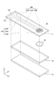
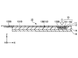
第1の実施形態に係る感圧部材について説明する。図1は、一実施形態に係る感圧部材の構成の一例を示す斜視図であり、図2は、一実施形態に係る感圧部材を分解斜視図であり、図3は、図1のI-I断面図である。図1~図3に示すように、感圧部材10は、弾性基材11と、接着層12と、一対の電極13A及び13Bと、粘着層14と、感圧導電性部材15と、剛性基材16とを備え、電極13Aと電極13Bとを電気的に接続する。以下、感圧部材10を構成する各部材について説明する。
第1の実施形態に係る感圧部材について説明する。図1は、一実施形態に係る感圧部材の構成の一例を示す斜視図であり、図2は、一実施形態に係る感圧部材を分解斜視図であり、図3は、図1のI-I断面図である。図1~図3に示すように、感圧部材10は、弾性基材11と、接着層12と、一対の電極13A及び13Bと、粘着層14と、感圧導電性部材15と、剛性基材16とを備え、電極13Aと電極13Bとを電気的に接続する。以下、感圧部材10を構成する各部材について説明する。
弾性基材11は、図1及び図2に示すように、平面視において矩形状に形成され、押圧力で弾性変形可能な板状部材である。弾性基材11は、押圧力が作用することによって変形し、押圧力が除荷されると元の形状に回復する弾性を有する基板である。弾性基材11は、互いに平行な一対の主面を有し、押圧力の作用する主面が作用面111であり、作用面111とは反対側の主面が押圧力を伝える伝達面112である。
弾性基材11は、エラストマーや合成樹脂を用いて形成することができる。エラストマーを形成する材料としては、例えば、天然ゴム、シリコーンゴム、クロロプレンゴム、イソプレンゴム、ブチルゴム、アクリルゴム、ニトリルゴム、ウレタンゴム、ポリイソブチレンゴム、ブタジエンゴム、スチレン-ブタジエンゴム、エチレン-プロピレンゴム、クロロスルホン化ポリエチレンゴム、エピクロルヒドリンゴム、ポリエステルゴム、フッ素ゴム、及びこれらの変性体等を用いることができる。合成樹脂としては、柔軟性エポキシ樹脂等を用いることができる。これらは、1種を単独で用いてもよいし、2種以上を組み合わせて用いてもよい。中でも、シリコーンゴムが好ましい。シリコーンゴムを用いることで、弾性基材11は、弾性が高く、接着層12との密着性を良好とすることができる。また、弾性基材11は、押圧力の作用点で弾性基材11が変形し、作用点が移動することなく押圧力を受け止めることができるので、押圧力は伝達面112から電極13A及び13Bと感圧導電性部材15に的確に伝達される。
弾性基材11の厚さは、10μm~100μmであることが好ましく、20μm~75μmであることがより好ましく、25μm~50μmであることがさらに好ましい。弾性基材11の厚さが10μm~100μmの範囲内であれば、弾性基材11は十分な強度を有すると共に、弾性を有することができる。
接着層12は、図3に示すように、弾性基材11の作用面111と反対側の伝達面112に設けられ、弾性基材11と電極13A及び13Bとの間に設けられる。接着層12は、弾性基材11と電極13A及び13Bとの接着力を高める機能を有し、電極13A及び13Bを固着する。
接着層12は、トリアジン系化合物を含む。接着層12としては、トリアジン系化合物を含む分子接着剤を用いて形成される。
トリアジン系化合物としては、トリアジンチオール化合物を用いることができる。トリアジンチオール化合物として、例えば、トリアジン環にチオール基(-SH基)又はチオール基のアルカリ金属塩がついたものを用いることができる。官能基の何れか一つは、ジブチルアミノ基、アニリノ基等の他の構造を有していてもよい。トリアジンチオール化合物の具体例としては、例えば、6-(3-トリエトキシシリルプロピルアミノ)-1,3,5-トリアジン-2,4-ジチオール、2,6-ジアジド-4-{3-(トリエトキシシリル)プロピルアミノ}-1,3,5-トリアジン、2-トリエトキシシリルプロピルアミノ-4-チオール-6-チオール-1,3,5-トリアジン、2-トリエトキシシリルプロピルアミノ-4-アジド-6-アジド-1,3,5-トリアジン、2-トリエトキシシリルプロピルアミノ-4-アミノエチルアミノ-6-アミノエチルアミノ-1,3,5-トリアジン、2-トリヒドロキシシリルプロピルアミノ-4-チオール-6-チオール-1,3,5-トリアジン、2-トリヒドロキシシリルプロピルアミノ-4-アジド-6-アジド-1,3,5-トリアジン、2-トリヒドロキシシリルプロピルアミノ-4-アミノエチルアミノ-6-アミノエチルアミノ-1,3,5-トリアジン、2-(4-メトキシフェニル)-4,6-ビス(トリクロロメチル)-1,3,5-トリアジン、2-(4-メトキシナフチル)-4,6-ビス(トリクロロメチル)-1,3,5-トリアジン、2-(4-エトキシナフチル)-4,6-ビス(トリクロロメチル)一1,3,5-トリアジン、2-(4-エトキシカルボニルナフチル)-4,6-ビス(トリクロロメチル)-1,3,5-トリアジン、2,4,6-トリス(モノクロロメチル)-1,3,5-トリアジン、2,4,6-トリス(ジクロロメチル)-1,3,5-トリアジン、2,4,6-トリス(トリクロロメチル)-1,3,5-トリアジン、2-メチル-4,6-ビス(トリクロロメチル)-1,3,5-トリアジン、2-n-プロピル-4,6-ビス(トリクロロメチル)-1,3,5-トリアジン、2-(α,α,β-トリクロロエチル)-4,6-ビス(トリクロロメチル)-1,3,5-トリアジン、2-フェニル-4,6-ビス(トリクロロメチル)-1,3,5-トリアジン、2-(p-メトキシフェニル)-4,6-ビス(トリクロロメチル)-1,3,5-トリアジン、2-(3,4-エポキシフェニル)-4、6-ビス(トリクロロメチル)-1,3,5-トリアジン、2-(p-クロロフェニル)-4,6-ビス(トリクロロメチル)-1,3,5-トリアジン、2-〔1-(p-メトキシフェニル)-2,4-ブタジエニル〕-4,6-ビス(トリクロロメチル)-1,3,5-トリアジン、2-スチリル-4,6-ビス(トリクロロメチル)-1,3,5-トリアジン、2-(p-メトキシスチリル)-4,6-ビス(トリクロロメチル)-1,3,5-トリアジン、2-(p-i-プロピルオキシスチリル)-4、6-ビス(トリクロロメチル)-1,3,5-トリアジン、2-(p-トリル)-4,6-ビス(トリクロロメチル)-1,3,5-トリアジン、2-(4-メトキシナフチル)-4,6-ビス(トリクロロメチル)-1,3,5-トリアジン、2-フェニルチオ-4,6-ビス(トリクロロメチル)-1,3,5-トリアジン、2-ベンジルチオ-4,6-ビス(トリクロロメチル)-1,3,5-トリアジン、4-(o-ブロモ-p-N,N-(ジエトキシカルボニルアミノ)-フェニル)-2,6-ジ(トリクロロメチル)-1,3,5-トリアジン、2,4,6-トリス(ジブロモメチル)-1,3,5-トリアジン、2,4,6-トリス(トリブロモメチル)-1,3,5-トリアジン、2-メチル-4,6-ビス(トリブロモメチル)-1,3,5-トリアジン、2-メトキシ-4,6-ビス(トリブロモメチル)-1,3,5-トリアジン、2,4,6-トリメルカプト-1,3,5-トリアジン、2-ジブチルアミノ-4,6-ジメルカプト-1,3,5-トリアジン、2-アニリノ-4,6-ジメルカプト-1,3,5-トリアジン及びこれらのナトリウム塩等が挙げられる。これらのナトリウム塩としては、2,4,6-トリメルカプト-1,3,5-トリアジンモノナトリウム塩等が挙げられる。これらは、一種単独で用いてもよいし、二種以上を併用してもよい。なお、1,3,5-トリアジンは、s-トリアジンともいう。
接着層12は、トリアジン系化合物を含む分子接着剤を用いて形成されるので、接着層12の厚さは、1nm~100nm程度である。なお、接着層12は、一般的な接着剤を用いて形成してもよい。この場合、接着層12の厚さは、1μm~20μmであることが好ましく、3μm~15μmであることがより好ましく、5μm~10μmであることがさらに好ましい。
一対の電極13A及び13Bは、図1及び図2に示すように、弾性基材11の伝達面112に接着層12を介して設けられている。図3に示すように、電極13A及び13Bは、互いに絶縁された状態で対向して設けられており、その先端が櫛歯状に形成された櫛歯電極を有している。電極13A及び13Bは、X軸方向に直線状に形成された本体部131A及び131Bと、櫛歯状に形成された先端部132A及び132B(櫛歯電極)と、外部の配線が連結される端子部133A及び133Bとを有する。
本体部131A及び131Bは、細長いパターン状に形成され、弾性基材11のY軸方向の辺の中間を通り、かつ弾性基材11のX軸方向の辺(Y軸方向の辺に直交する辺)に平行な中心線に対して略対称となるように設けられている。その両端側には、先端部132A及び132Bと端子部133A及び133Bとが電気的に接続されて形成されている。
先端部132A及び132Bは、平面視において+X軸方向側であって感圧導電性部材15の位置に設けられ、先端部132A及び132Bの、複数の櫛歯がX軸方向に沿って、交互に配列されて、互いに絶縁されるように配置されている。この櫛歯間のギャップは狭い間隔となっている。
端子部133A及び133Bは、矩形の形状に形成され、平面視において、-X軸方向側の弾性基材11の端部の位置に設けられる。この端子部133A及び133Bには、粘着層14が被覆されていない。また、本実施形態では、図3に示すように、剛性基材16も対向して配置されていない。
電極13A及び13Bの本体部131A及び131Bの大部分は、弾性基材11と粘着層14との間に配置され、先端部132A及び132Bは、弾性基材11と感圧導電性部材15との間に配置されている。すなわち、電極13A及び13Bの本体部131A及び131Bの大部分と先端部132A及び132Bは、これらを挟持するように弾性基材11と粘着層14又は感圧導電性部材15との間に配置されている。
電極13A及び13Bを形成する材料としては、金(Au)、銀(Ag)、銅(Cu)、ニッケル(Ni)、鉄(Fe)、アルミニウム(Al)、錫(Sn)、鉛(Pb)、クロム(Cr)及びコバルト(Co)等の各種金属;これらの合金;カーボンブラック、グラファイト(黒鉛)、カーボンナノチューブ、カーボンファイバー(炭素繊維)、及びフラーレン等の炭素系材料等が挙げられる。電極13A及び13Bを形成する材料は、これらを、一種単独で用いてもよいし、二種以上を併用してもよい。これらの中でも、接続の安定性、製造コストの低減、及び作製のし易さ等の点から、電極13A及び13Bを形成する材料としては、Ag又はCuを用いることが好ましい。電極13A及び13Bは、1つの金属層で形成されていてもよいし、複数の金属層を積層して構成されていてもよい。
また、電極13A及び13Bは、電極13A及び13Bを形成する材料を導電性部材として用い、合成樹脂等のバインダーに分散させたコンポジット皮膜で構成してもよい。その際に、バインダーとして合成樹脂を用いる場合は、弾性基材11と同様なエラストマーを用いるのが好適である。これにより、弾性基材11の局所的な変形に追従し易い先端部132A及び132Bを有する電極13A及び13Bが得られる。
電極13A及び13Bの厚さは、1μm~50μmであることが好ましく、5μm~30μmであることがより好ましく、10μm~20μmであることがさらに好ましい。電極13A及び13Bの厚さが1μm~50μmの範囲内であれば、導電性を十分確保できる。また、電極13A及び13Bの厚さは、流す電流の大きさに対応して決められるが、50μm以上にしてもよい。
粘着層14は、弾性基材11の伝達面112側に、電極13A及び13B(本体部131A及び131Bの大部分)と、感圧導電性部材15を被覆するように設けられる。
粘着層14としては、例えば、シリコーン系粘着剤、アクリル系粘着剤、及びウレタン系粘着剤等を用いることができる。粘着層14は、上記の何れかの粘着材を用いて形成された両面粘着シートや上記の何れかの粘着材と不織布からなる両面粘着テープを用いることが好ましい。粘着層14を両面粘着シートや両面粘着テープとすることで、弾性基材11の伝達面112と剛性基材16との密着性を向上させることができる。
粘着層14の厚さは、適宜設計可能であり、0.08mm~0.12mmであることが好ましい。粘着層14の厚さが0.05mm~0.20mmの範囲内であれば、粘着層14は、十分な粘着力を有すると共に、感圧部材10の厚さを抑えることができる。
感圧導電性部材15は、電極13A及び13Bの先端部132A及び132Bと粘着層14との間に配置され、先端部132A及び132Bの表面に、感圧部材10の高さ方向(Z軸方向)に積層するように設けられ、電極13A及び13Bと電気的に接続可能としている。感圧導電性部材15は、弾性変形可能であり、押圧力の変化により弾性変形して、その部分の抵抗値が低下する機能を有する。そして、この感圧導電性部材15に接触している電極13A及び13B同士が通電するようになり、電極13A及び13B間の電気抵抗値が押圧力に応じて変化することになる。すなわち、押圧力の変化に応じて、感圧導電性部材15の抵抗値が変化すると共に、感圧導電性部材15と電極13A及び13Bとの接触抵抗も変化するので、押圧力の変化を抵抗値変化として捉えることができる。
感圧導電性部材15は、円錐台形(切頭円錐形)に形成され、大きい面が電極13A及び13Bと接し、小さい面が粘着層14と接するように配置されている。これにより、押圧力を加える面積を広くできると共に、電極13A及び13Bの先端部132A及び132Bへの単位面積当たりの荷重が強まる。
感圧導電性部材15は、平面視においてその上面が電極13A及び13Bの先端部132A及び132Bを覆う大きさとなるように形成される。感圧導電性部材15の上面が先端部132A及び132Bの全面を覆うように形成されることで、弾性基材11に加えられた押圧力を感圧導電性部材15に確実に伝えられる。
感圧導電性部材15は、粒子状の導電性材料151をエラストマー152に含有する導電性エラストマーを用いて形成できる。感圧導電性部材15が、導電性材料151を含有する導電性エラストマーであれば、導電性材料151による導通に加え、押圧力に対して変形及び復元がし易い。感圧導電性部材15は、導電性材料151をエラストマー152中にほぼ均一に分散させて含むことが好ましい。
導電性材料151としては、金属粒子や炭素系材料等の導電性を有する材料を用いることができる。金属粒子や炭素系材料としては、上述の電極13A及び13Bと同様の材料を用いることができる。
導電性材料151の平均粒子径としては、0.05μm~200μmが好ましく、0.5μm~60μmがより好ましく、1.0μm~30μmがさらに好ましい。導電性材料151の平均粒子径が0.05μm~200μmの範囲内であれば、導電性材料151の凝集を抑えてエラストマー152内での分散性を高めることができる。また、感圧導電性部材15が弾性変形した際に、導電性材料151の感圧導電性部材15内での移動が相対的に小さくなることを抑えることで、弾性変形による抵抗の変化が緩慢になるのを低減できる。なお、平均粒子径とは、有効径による体積平均粒径をいい、平均粒子径は、例えば、レーザ回折・散乱法又は動的光散乱法等によって測定される。
エラストマー152としては、弾性基材11と同様のエラストマーを用いることができる。
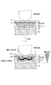
感圧導電性部材15は、図4に示すように、押圧部材等による押圧力が作用していない状態では、互いに接触する導電性材料151の数は少なく、導電経路がほとんど形成されていない(図4中、白丸参照)ので、感圧導電性部材15は、非常に大きな抵抗値を有する。そして、感圧導電性部材15に押圧力が作用すると、導電性材料151は互いに接近し、互いに接触する導電性材料151の数が多くなるので、感圧導電性部材15の平面方向及び垂直方向等に導電経路(図4中、黒丸参照)が形成され、感圧導電性部材15の抵抗値が小さくなる。このように、押圧力によって感圧導電性部材15は変形し、導電性材料151同士が接触又は離間することで、感圧導電性部材15の抵抗値が変化する。
感圧導電性部材15は、ゴム硬度が30~70の範囲内であることが好ましく、50~60の範囲内であることがより好ましい。ゴム硬度が40~70の範囲内であれば、感圧導電性部材15は十分な強度を有することができ、高い復元力を発揮できる。なお、ゴム硬度とは、日本工業規格JIS K6301で規定された値である。
感圧導電性部材15の厚さは、0.1mm~10mmであることが好ましく、0.5mm~5mmであることがより好ましく、0.7mm~3mmであることがさらに好ましい。感圧導電性部材15の厚さが0.1mm~10mmの範囲内であれば、感圧導電性部材15は十分な強度を有すると共に、弾性を有することができる。
剛性基材16は、粘着層14を弾性基材11と狭持するように設けられ、押圧力を確実に受け止めて感圧導電性部材15の変形が確実に行われるための機能を有している。剛性基材16は、例えば、板状のものである。なお、本実施形態では、感圧部材10は、剛性基材16を備えるが、例えば、何かの筐体に貼り付けて使用する場合は、感圧部材10は、剛性基材16を備えていなくてもよい。
剛性基材16を形成する材料としては、ポリアミド(PA)、ポリイミド(PI)、ポリブチレンテレフタレート(PET)、ポリエチレンナフタレート(PEN)、ポリエーテルイミド(PEI)、ポリエーテルサルフォン(PES)、ポリスチレン(PS)、ポリメチルメタクリレート(PMMA)、ポリエチレンニトリル、ポリエーテルエーテルケトン(PEEk)、ポリフェニレンサルファイド(PPS)、フェノール、エポキシ(ガラスフィラー入り)及びポリカーボネート(PC)等の合成樹脂を用いることができる。これらは、一種単独で用いてもよいし、二種以上を併用してもよい。これらの中でも、耐熱性等の観点から、ポリイミド、又はポリエチレンテレフタレート等を用いることが好ましい。
剛性基材16を形成する材料としては、上記の合成樹脂以外に、Al、Mg、Cu、Ni、Co、Cr、Fe、Zn、Pb、及びTi等の金属、及びこれらの合金;Al、Mg、Si、Ge、及びBe等の金属酸化物;窒化珪素(Si3N4)、窒化ボロン(BN)、及び炭化珪素(SiC)等の金属窒化物;ガラス材料等を用いることもできる。
剛性基材16の厚さは、適宜設計可能であり、材料の種類にもよるが、剛性の弱い合成樹脂材料であれば、0.5mm~1.5mmであることが好ましく、剛性の強い金属材料であれば、0.1mm~0.5mmであることが好ましい。この範囲内であれば、剛性基材16は十分な強度を有することができる。
本実施形態に係る感圧部材10の製造方法について説明する。平面視において所定の大きさに切り出した弾性基材11を準備する。準備した弾性基材11の表面を水やアルコール、アセトン等の洗浄液で洗浄し、弾性基材11の表面に付着している汚れや異物等を除去する。その後、弾性基材11の伝達面112に、トリアジン系化合物を含む分子接着剤を塗布して乾燥することで、接着層12を形成する。その後、接着層12の表面に、Ag粒子やCu粒子等の導電性を有する材料を含む塗布液(ペースト)を塗布して、電極13A及び13Bを形成する。電極13A及び13Bは接着層12により固着される。電極13A及び13Bの形成方法としては、導電性を有する材料を含む塗布液を塗布する塗布法の他に、無電解めっき法、電気めっき法、スパッタ、又は蒸着を用いる方法等により、金属めっき皮膜を形成する方法等を用いてもよい。
次に、平面視において、電極13A及び13Bの先端部132A及び132Bの表面に感圧導電性部材15を設置した後、伝達面112に、電極13A及び13Bの一部と感圧導電性部材15とを被覆するように粘着層14を設ける。その後、粘着層14の表面に剛性基材16を設置して、弾性基材11と剛性基材16とで粘着層14を挟み込む。
これにより、本実施形態に係る感圧部材10が得られる。
感圧部材10は、上述の通り、弾性基材11と、電極13A及び13Bと、感圧導電性部材15とを備え、弾性基材11は押圧力の作用する作用面111を有する。電極13A及び13Bと感圧導電性部材15は、弾性基材11の伝達面112から下方向に電極13A及び13Bと感圧導電性部材15との順に積層されている。感圧導電性部材15は、エラストマー152に導電性材料151を分散して含んだ状態で構成されている。図5に示すように、感圧部材10に押圧部材等により押圧力が作用していない状態では、電極13A及び13Bと導電性材料151は殆ど接触しておらず、電極13A及び13B同士は殆ど導通していないため、感圧導電性部材15は高い抵抗値を有する。
感圧部材10に押圧部材等により押圧力が作用すると、感圧導電性部材15の上面側には圧縮応力が生じ、下面側は押圧力が減衰して小さくなる。上面側は、この圧縮応力の作用により、感圧導電性部材15中に含まれる導電性材料151同士が近接し始め、導電性材料151が密な状態となる。これにより、電極13A及び13Bと導電性材料151が接触し、導通経路が多数形成され、感圧導電性部材15の抵抗値は低くなる。感圧部材に作用する押圧力の大きさによって、形成される導通経路が三次元的に大きくなったり小さくなったりするため、押圧力を抵抗値により検出することができる。一方、感圧導電性部材15の下面側は、感圧導電性部材15に作用する押圧力が減衰して小さくなるため、感圧導電性部材15中の導電性材料151同士は離間した状態のままであり、押圧力が作用する前と導電性材料151同士の距離は殆ど変化しない。または、感圧導電性部材15の下面に小さい引張応力が生じ、導電性材料151同士の距離が大きくなり易い。そのため、感圧導電性部材15の下面側では、感圧導電性部材15内に導通経路が殆ど形成されない。
また、感圧部材10は、伝達面112から下方向に電極13A及び13Bと感圧導電性部材15との順に積層されているので、図5に示すように、弾性基材11の作用面111に押圧力が作用すると、作用面111に加わった押圧力が減衰する前に伝達面112から感圧導電性部材15に作用させることができる。また、感圧導電性部材15に作用した押圧力によって、感圧導電性部材15の電極13A及び13Bの設置面側の近傍領域が潰れるように変形することで、感圧導電性部材15の電極13A及び13Bの設置面側に圧縮応力が働き、感圧導電性部材15内、特に感圧導電性部材15の電極13A及び13Bの設置面側の近傍領域を通電させることができる。これにより、一対の電極13A及び13B同士の間を流れる電流を生じさせることができる。
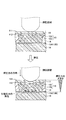
一方、例えば、図6に示すように、感圧部材が、弾性基材11の伝達面112から、感圧導電性部材15と、粘着層14と、電極13A及び13Bと、剛性基材16とをこの順に積層し、感圧導電性部材15の下側に電極13A及び13Bが配置されているとする。この場合、押圧力が感圧導電性部材15で減衰して電極に伝わり、電流が流れることになる。そのため、作用面111に加わった押圧力に対する感度が高くなり難い傾向にある。また、電極13A及び13Bの感圧導電性部材15との接触面には、引張応力が働くため、感圧導電性部材15内の導電性材料151同士の間隔が狭くなり難く、導通が取れ難くなる可能性がある。
よって、感圧部材10は、上述の通り、弾性基材11の作用面111に加わった押圧力を感圧導電性部材15の電極13A及び13Bの設置面側に押圧力の大きさを極力維持した状態で伝えることができるので、検出感度を高めると共に、押圧力の大きさのばらつきを抑えることができる。したがって、感圧部材10は、外部から加わる押圧力を高感度で安定して検出することができる。
また、感圧部材10は、電極13A及び13Bを弾性基材11と感圧導電性部材15との間に設けることで、感圧導電性部材15の厚みが弾性基材11の作用面111に加わった押圧力の大きさを低減することなく、電極13A及び13Bに伝えることができる。そのため、感圧部材10は、感圧導電性部材15の厚さを厚くすることができるので、押圧力を受けられる範囲を広げることができる。
感圧部材10は、弾性基材11と電極13A及び13Bとの間に、トリアジン系化合物を含む接着層12を含むことができる。これにより、感圧部材10は、弾性基材11と電極13A及び13Bとの接着力を高めることができる。そのため、感圧部材10は、弾性基材11に繰り返しの変形動作が加わったとしても、弾性基材11と電極13A及び13Bとの剥離を抑制することができる。
感圧部材10は、伝達面112に、粘着層14と剛性基材16とを有し、粘着層14は弾性基材11の伝達面112に電極13A及び13Bと感圧導電性部材15を被覆し、剛性基材16は粘着層14を弾性基材11と挟持するように設けることができる。感圧導電性部材15は、弾性基材11と剛性基材16との間に挟み込んだ状態で配置されるので、押圧力を剛性基材16で受け止めて感圧導電性部材15に確実に伝えることができる。よって、感圧部材10は、感圧導電性部材15に押圧力を安定して伝えることができる。
また、感圧部材10は、剛性基材16を備えることで、強度が向上し、形状が保持し易くなるため、感圧部材10の取り扱い易さを向上させることができる。
感圧部材10は、感圧導電性部材15として、エラストマー152に導電性材料151を含有する導電性エラストマーを用いることができる。感圧導電性部材15が導電性エラストマーであれば、導電性材料151による導通に加え、押圧力に対して変形及び復元がし易いので、電極13A及び13B同士の間を通電させ易くすることができると共に、押圧力に対する応答性を向上させることができる。
感圧部材10は、電極13A及び13Bを、平面視において、感圧導電性部材15の位置にある先端部132A及び132Bの形状を櫛歯状に形成できる。電極13A及び13Bは、先端部132A及び132Bの形状を櫛歯状に形成し、複数の櫛歯をX軸方向に沿って交互に配列させることで、先端部132A及び132Bの間隔を略均等に狭い状態を維持できる。そのため、弾性基材11の作用面111に押圧力が作用して感圧導電性部材15が変形した際、感圧導電性部材15の導通が取れた部分で電極13A及び13B同士が通電し易くなる。よって、押圧力が弾性基材11の作用面111に加わった際に、電極13A及び13B間に導通が取り易くなる。
一実施形態に係る感圧部材10は、上記にように、外部から加わる押圧力を高感度で安定して検出でき、簡単な構成で、触れた時の感触も良好とすることができる。そのため、感圧部材10は、圧力検出装置(感圧センサ)として、ロボットの触覚センサ、又は電子機器のタッチパネル等に好適に用いることができる。電子機器としては、例えば、情報携帯端末、携帯電話、パーソナルコンピューター、デジタルカメラ、ビデオカメラ、カーナビゲーション、電子手帳、電卓、テレビ電話等のタッチパネルを備えた機器等が挙げられる。
<圧力検出装置>
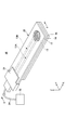
一実施形態に係る感圧部材10を適用した圧力検出装置について説明する。図7は、感圧部材10を適用した圧力検出装置の斜視図であり。図8は、図7のII-II断面図である。図7及び図8に示すように、圧力検出装置30は、感圧部材10と、接続部31と、検出部32とを備える。
一実施形態に係る感圧部材10を適用した圧力検出装置について説明する。図7は、感圧部材10を適用した圧力検出装置の斜視図であり。図8は、図7のII-II断面図である。図7及び図8に示すように、圧力検出装置30は、感圧部材10と、接続部31と、検出部32とを備える。
接続部31は、感圧部材10の弾性基材11、接着層12、並びに電極13A及び13Bの一端部(-Y軸方向)を挟持し、電極13A及び13Bと電気的に接続可能に連結されている。接続部31は、電極13A及び13Bのそれぞれと接続しつつ、電極13A及び13Bに流れる電流を配線34を介して検出部32に流す機能を有している。
検出部32は、接続部31と配線34を介して感圧部材10と接続されている。検出部32は、接続部31から送られてきた電流を電気信号として検知することで、感圧部材10での抵抗値の変化を検出する。
感圧部材10の弾性基材11が押圧されて、電極13A及び13Bに電流変化(抵抗値の変化)が生じると、電極13A及び13B間の電流は、接続部31及び配線34を介して検出部32に送られ、電気信号に変換される処理が行われる。そして、感圧部材10での抵抗値の変化を検知して圧力値を算出する。
圧力検出装置30は、感圧部材10を備えているので、感圧部材10が押圧された際、押圧力を高感度で安定して検出することができる。
(変形例)
本実施形態では、接着層12が特になくても、伝達面112に電極13A及び13Bを固着できる場合等には、感圧部材10は接着層12を備えなくてもよい。
本実施形態では、接着層12が特になくても、伝達面112に電極13A及び13Bを固着できる場合等には、感圧部材10は接着層12を備えなくてもよい。
本実施形態では、接着層12は、電極13A及び13Bを固着できれば、伝達面112のうちの、電極13A及び13Bと接する部分の少なくとも一部に形成されていてもよい。
本実施形態では、電極13A及び13Bは、先端部132A及び132Bを櫛歯電極とし、それぞれ対向させているが、これに限るものでは無い。例えば、電極13A及び13Bは、先端部132A及び132Bを平面視において渦巻き状に形成し、それぞれ絶縁性を保ちながら対向して配置させてもよいし、ミアンダ形状に形成された電極をそれぞれ絶縁性を保ちながら対向して配置させても良い。
本実施形態では、剛性基材16は、布等で形成されていてもよい。
以下、実施例及び比較例を示して実施形態を更に具体的に説明するが、実施形態はこれらの実施例及び比較例により限定されるものではない。
<実施例1>
[感圧部材の作製]
シリコーンゴム(「極薄SRシート」、アズワン社製、厚さ0.1mm)から所定の大きさに切り出した弾性基材11(図1参照)を準備した。この準備した弾性基材11をエタノール溶液に浸漬して30秒間洗浄して、コロナ放電を20秒行った後、弾性基材11の一方の主面に分子接着剤を塗布して乾燥することで、接着層12(図3参照)を形成した。その後、接着層12の表面に、Agインク(「SSP2801」、東洋紡社製)を塗布して、図2に示すように、先端が櫛歯状となるように配置された一対の電極13A及び13Bを形成した。その後、一対の電極13A及び13Bの先端部分に、感圧導電性部材15を配置し、粘着層14として両面粘着テープ(「No.7082」、寺岡製作所社製)を貼り付け、両面粘着テープの上にフェノール樹脂からなる剛性基材16(「スミライトPL-1147」、住友ベークライト社製、厚さ:1mm)を貼り合わせた。これにより、図1に示す感圧部材10を作製した。
[感圧部材の作製]
シリコーンゴム(「極薄SRシート」、アズワン社製、厚さ0.1mm)から所定の大きさに切り出した弾性基材11(図1参照)を準備した。この準備した弾性基材11をエタノール溶液に浸漬して30秒間洗浄して、コロナ放電を20秒行った後、弾性基材11の一方の主面に分子接着剤を塗布して乾燥することで、接着層12(図3参照)を形成した。その後、接着層12の表面に、Agインク(「SSP2801」、東洋紡社製)を塗布して、図2に示すように、先端が櫛歯状となるように配置された一対の電極13A及び13Bを形成した。その後、一対の電極13A及び13Bの先端部分に、感圧導電性部材15を配置し、粘着層14として両面粘着テープ(「No.7082」、寺岡製作所社製)を貼り付け、両面粘着テープの上にフェノール樹脂からなる剛性基材16(「スミライトPL-1147」、住友ベークライト社製、厚さ:1mm)を貼り合わせた。これにより、図1に示す感圧部材10を作製した。
[押し込み時の圧力及び抵抗の評価]
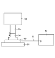
図9に示すように、作製した感圧部材10を試験台51の上に設置した後、感圧部材10の一対の電極を配線52で測定機53につなぎ、感圧部材50の弾性基材11の上に圧子54を載せた。その後、圧子54にピン55を当てて荷重計56で押し込み速度0.1mm/分として押し込み、押し込んでいる時の時間と圧力及び抵抗値との関係を測定し、圧力と抵抗値との関係を求めた。圧力と抵抗値との関係を図10に示す。
図9に示すように、作製した感圧部材10を試験台51の上に設置した後、感圧部材10の一対の電極を配線52で測定機53につなぎ、感圧部材50の弾性基材11の上に圧子54を載せた。その後、圧子54にピン55を当てて荷重計56で押し込み速度0.1mm/分として押し込み、押し込んでいる時の時間と圧力及び抵抗値との関係を測定し、圧力と抵抗値との関係を求めた。圧力と抵抗値との関係を図10に示す。
<比較例1~3>
比較例1~3において、感圧部材として、公知の感圧部材を用いたこと以外は、実施例1と同様な方法で行った。公知の感圧部材として、一対の電極が形成された剛性基板上に感圧導電性部材と粘着層が積層され、更に弾性基板が積層されている感圧部材を用いた。なお、実施例1の感圧部材10と比較例1~3の感圧部材との違いは、一対の電極が形成されている位置が異なっているところである。つまり、実施例1の感圧部材10は、弾性基材11と感圧導電性部材15との間に設けられており、比較例1~3の感圧部材は、剛性基板と感圧導電性部材との間に設けられている。また、比較例1では、インターリンク社製の「FSR-402」を用い、比較例2では、ALHPA社製の「MF01-N-221-A01」を用い、比較例3では、マルサンネーム社製の「MK-C」を用いた。圧力(荷重)と抵抗値との関係を、比較例1及び2については図10に示し、比較例3については図11に示す。
比較例1~3において、感圧部材として、公知の感圧部材を用いたこと以外は、実施例1と同様な方法で行った。公知の感圧部材として、一対の電極が形成された剛性基板上に感圧導電性部材と粘着層が積層され、更に弾性基板が積層されている感圧部材を用いた。なお、実施例1の感圧部材10と比較例1~3の感圧部材との違いは、一対の電極が形成されている位置が異なっているところである。つまり、実施例1の感圧部材10は、弾性基材11と感圧導電性部材15との間に設けられており、比較例1~3の感圧部材は、剛性基板と感圧導電性部材との間に設けられている。また、比較例1では、インターリンク社製の「FSR-402」を用い、比較例2では、ALHPA社製の「MF01-N-221-A01」を用い、比較例3では、マルサンネーム社製の「MK-C」を用いた。圧力(荷重)と抵抗値との関係を、比較例1及び2については図10に示し、比較例3については図11に示す。
図10及び図11に示すように、比較例1~3では、最低でも12kPa以上の圧力がかからないと抵抗は下がらず、圧力が最低でも40kPa以上の圧力にならないと、抵抗が安定しなかったことが確認された。一方、実施例1では、約3kPaの圧力で抵抗は下がり、約16kPaの圧力で抵抗が安定していたことが確認された。
よって、一実施形態の感圧部材は、小さい押圧力でも早期に高感度で安定して検出することができるといえる。
以上の通り、実施形態を説明したが、上記実施形態は、例として提示したものであり、上記実施形態により本発明が限定されるものではない。上記実施形態は、その他の様々な形態で実施されることが可能であり、発明の要旨を逸脱しない範囲で、種々の組み合わせ、省略、置き換え、変更等を行うことが可能である。これら実施形態やその変形は、発明の範囲や要旨に含まれると共に、特許請求の範囲に記載された発明とその均等の範囲に含まれる。
本出願は、2019年3月25日に日本国特許庁に出願した特願2019-57497号に基づく優先権を主張するものであり、特願2019-57497号の全内容を本出願に援用する。
10、50 感圧部材
11 弾性基材
111 作用面
112 伝達面
12 接着層
13A、13B 電極
131A、131B 本体部
132A、132B 先端部
14 粘着層
15 感圧導電性部材
16 剛性基材
30 圧力検出装置
31 接続部
32 検出部
34 配線
11 弾性基材
111 作用面
112 伝達面
12 接着層
13A、13B 電極
131A、131B 本体部
132A、132B 先端部
14 粘着層
15 感圧導電性部材
16 剛性基材
30 圧力検出装置
31 接続部
32 検出部
34 配線
Claims (6)
- 押圧力の作用する作用面を有し、前記押圧力で弾性変形可能な弾性基材と、
前記弾性基材の前記作用面と反対側の伝達面に設けられた、一対の電極と、
前記一対の電極と電気的に接続可能に前記伝達面に設けられた感圧導電性部材と、を備え、
前記感圧導電性部材が前記押圧力の変化により弾性変形し、前記一対の電極間の電気抵抗値が変化することを特徴とする感圧部材。 - 前記弾性基材と前記電極との間に、トリアジン系化合物を含む接着層を含むことを特徴とする請求項1に記載の感圧部材。
- 前記感圧導電性部材が、エラストマーに導電性材料を含有する導電性エラストマーであることを特徴とする請求項1又は2に記載の感圧部材。
- 前記伝達面に、前記電極及び前記感圧導電性部材を被覆するように設けられる粘着層と、
前記粘着層を前記弾性基材と狭持するように設けられる剛性基材と、
を有することを特徴とする請求項1~3の何れか一項に記載の感圧部材。 - 前記一対の電極は、平面視において、前記感圧導電性部材の位置における形状が櫛歯状に形成されていることを特徴とする請求項1~4の何れか一項に記載の感圧部材。
- 請求項1~5の何れか一項に記載の感圧部材と、
前記感圧部材からの信号を取り出す接続部と、
前記接続部に接続されて、前記信号を処理する検出部と、
を備えることを特徴とする圧力検出装置。
Priority Applications (1)
| Application Number | Priority Date | Filing Date | Title |
|---|---|---|---|
| JP2021508830A JPWO2020195460A1 (ja) | 2019-03-25 | 2020-02-25 |
Applications Claiming Priority (2)
| Application Number | Priority Date | Filing Date | Title |
|---|---|---|---|
| JP2019057497 | 2019-03-25 | ||
| JP2019-057497 | 2019-03-25 |
Publications (1)
| Publication Number | Publication Date |
|---|---|
| WO2020195460A1 true WO2020195460A1 (ja) | 2020-10-01 |
Family
ID=72609187
Family Applications (1)
| Application Number | Title | Priority Date | Filing Date |
|---|---|---|---|
| PCT/JP2020/007488 Ceased WO2020195460A1 (ja) | 2019-03-25 | 2020-02-25 | 感圧部材及び圧力検出装置 |
Country Status (2)
| Country | Link |
|---|---|
| JP (1) | JPWO2020195460A1 (ja) |
| WO (1) | WO2020195460A1 (ja) |
Citations (4)
| Publication number | Priority date | Publication date | Assignee | Title |
|---|---|---|---|---|
| JP2006513408A (ja) * | 2003-01-07 | 2006-04-20 | アイイーイー インターナショナル エレクトロニクス アンド エンジニアリング エス.エイ. | 微細構造化面をもつ弾性センサ層で構成される圧力センサ |
| JP2009298063A (ja) * | 2008-06-16 | 2009-12-24 | Nippon Zeon Co Ltd | 積層体及び配線基板 |
| JP2012159463A (ja) * | 2011-02-02 | 2012-08-23 | Canon Chemicals Inc | 感圧センサ体 |
| US20120256720A1 (en) * | 2011-04-08 | 2012-10-11 | Samsung Electronics Co., Ltd. | Bending sensor and method for fabricating the same |
Family Cites Families (8)
| Publication number | Priority date | Publication date | Assignee | Title |
|---|---|---|---|---|
| DE19533756A1 (de) * | 1995-09-12 | 1997-03-13 | Fraunhofer Ges Forschung | Elektronisches Bauelement zur statischen und dynamischen Druckerfassung |
| JPH1183644A (ja) * | 1997-09-08 | 1999-03-26 | Toyo Polymer Kk | 感圧センサー |
| GB2335310B (en) * | 1998-03-11 | 2001-09-19 | Draftex Ind Ltd | Force-responsive detectors and systems |
| JP2001195945A (ja) * | 2000-01-06 | 2001-07-19 | Polymatech Co Ltd | 感圧導電センサー |
| JP5700838B2 (ja) * | 2009-08-28 | 2015-04-15 | 日本写真印刷株式会社 | 圧力検出装置 |
| JP5636290B2 (ja) * | 2011-01-12 | 2014-12-03 | キヤノン化成株式会社 | 感圧センサ |
| JP2014163815A (ja) * | 2013-02-26 | 2014-09-08 | Seiko Epson Corp | 力検出装置およびロボット |
| JP2017009559A (ja) * | 2015-06-26 | 2017-01-12 | ヤマハ株式会社 | 歪みセンサ素子 |
-
2020
- 2020-02-25 JP JP2021508830A patent/JPWO2020195460A1/ja active Pending
- 2020-02-25 WO PCT/JP2020/007488 patent/WO2020195460A1/ja not_active Ceased
Patent Citations (4)
| Publication number | Priority date | Publication date | Assignee | Title |
|---|---|---|---|---|
| JP2006513408A (ja) * | 2003-01-07 | 2006-04-20 | アイイーイー インターナショナル エレクトロニクス アンド エンジニアリング エス.エイ. | 微細構造化面をもつ弾性センサ層で構成される圧力センサ |
| JP2009298063A (ja) * | 2008-06-16 | 2009-12-24 | Nippon Zeon Co Ltd | 積層体及び配線基板 |
| JP2012159463A (ja) * | 2011-02-02 | 2012-08-23 | Canon Chemicals Inc | 感圧センサ体 |
| US20120256720A1 (en) * | 2011-04-08 | 2012-10-11 | Samsung Electronics Co., Ltd. | Bending sensor and method for fabricating the same |
Also Published As
| Publication number | Publication date |
|---|---|
| JPWO2020195460A1 (ja) | 2020-10-01 |
Similar Documents
| Publication | Publication Date | Title |
|---|---|---|
| TWI578859B (zh) | 印刷電路板及印刷電路板的製造方法 | |
| JP6269337B2 (ja) | プローブピン、および、これを用いた電子デバイス | |
| TWI545472B (zh) | 壓力檢測部及具備壓力檢測部的資訊輸入裝置 | |
| CN102483363B (zh) | 压力检测单元以及压力检测装置 | |
| WO2020195461A1 (ja) | 感圧部材及び圧力検出装置 | |
| CN107683633B (zh) | 印制布线板、印制布线板用补强件及印制基板 | |
| US20190373775A1 (en) | Heat conductive sheet and multilayered heat conductive sheet | |
| JP5281551B2 (ja) | 静電容量式入力装置 | |
| CN109983628A (zh) | 导电粒子配置膜、其制造方法、检查探头单元、导通检查方法 | |
| JP6454439B1 (ja) | 感圧センサ | |
| US12078512B2 (en) | Dual channel detector with different measurement signals | |
| CN110266301B (zh) | 含传感器片的电子设备用壳体及传感器片用的安装板 | |
| JP2007315875A (ja) | 感圧センサ | |
| CN106066182B (zh) | 编码器标尺及其制造与附接方法 | |
| JP2017009559A (ja) | 歪みセンサ素子 | |
| WO2026092354A1 (zh) | 电子设备 | |
| JP2008091950A (ja) | 電気装置 | |
| JP6066049B2 (ja) | コンタクト手段を直接コンタクティングする装置および圧力測定セル用の付属の接続装置 | |
| CN109642126B (zh) | 压敏胶带、其制造方法及包括其的电子设备 | |
| CN106165202A (zh) | 端子连接构造及半导体装置 | |
| KR100997108B1 (ko) | 촉각센서와 그 제조방법 | |
| WO2012008541A1 (ja) | コンタクトプローブおよびプローブユニット | |
| KR101178791B1 (ko) | 저항형 촉각센서와 그 제조방법 | |
| JP2016206163A (ja) | エンコーダスケール及びその製造・取付方法 | |
| JP2015215306A (ja) | 感圧センサ及びその製造方法 |
Legal Events
| Date | Code | Title | Description |
|---|---|---|---|
| 121 | Ep: the epo has been informed by wipo that ep was designated in this application |
Ref document number: 20776406 Country of ref document: EP Kind code of ref document: A1 |
|
| ENP | Entry into the national phase |
Ref document number: 2021508830 Country of ref document: JP Kind code of ref document: A |
|
| NENP | Non-entry into the national phase |
Ref country code: DE |
|
| 122 | Ep: pct application non-entry in european phase |
Ref document number: 20776406 Country of ref document: EP Kind code of ref document: A1 |