WO2020194812A1 - Laminated varistor - Google Patents
Laminated varistor Download PDFInfo
- Publication number
- WO2020194812A1 WO2020194812A1 PCT/JP2019/040562 JP2019040562W WO2020194812A1 WO 2020194812 A1 WO2020194812 A1 WO 2020194812A1 JP 2019040562 W JP2019040562 W JP 2019040562W WO 2020194812 A1 WO2020194812 A1 WO 2020194812A1
- Authority
- WO
- WIPO (PCT)
- Prior art keywords
- pair
- layer
- high resistance
- varistor
- sintered body
- Prior art date
Links
Images


Classifications
-
- H—ELECTRICITY
- H01—ELECTRIC ELEMENTS
- H01C—RESISTORS
- H01C7/00—Non-adjustable resistors formed as one or more layers or coatings; Non-adjustable resistors made from powdered conducting material or powdered semi-conducting material with or without insulating material
- H01C7/10—Non-adjustable resistors formed as one or more layers or coatings; Non-adjustable resistors made from powdered conducting material or powdered semi-conducting material with or without insulating material voltage responsive, i.e. varistors
- H01C7/105—Varistor cores
- H01C7/108—Metal oxide
- H01C7/112—ZnO type
Definitions
- the present invention relates to a laminated varistor used in various electronic devices.
- the laminated varistor includes a sintered body, a pair of external electrodes provided on the sintered body, and a high resistance layer provided on the sintered body.
- the sintered body has a varistor layer containing ZnO as a main component and containing Bi, and a pair of internal electrodes embedded in the varistor layer.
- the sintered body has a pair of end faces from which a pair of internal electrodes are derived, and a surface on which a pair of internal electrodes other than the pair of end faces are not exposed.
- the pair of external electrodes are provided on each of the pair of end faces of the sintered body and are electrically connected to the pair of internal electrodes.
- the high resistance layer is provided on the above-mentioned surface where the pair of internal electrodes of the sintered body is not exposed.
- the high resistance layer has a specific resistance that is four times or more the specific resistance of the portion of the varistor layer sandwiched between the pair of internal electrodes.
- the thickness of the high resistance layer is 50 ⁇ m or
- This laminated varistor can be miniaturized while ensuring surge resistance, and the external electrodes can be plated stably.
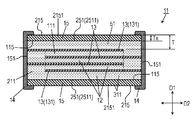
- FIG. 1 is a perspective view of a laminated varistor according to an embodiment.
- FIG. 2 is a cross-sectional view taken along the line II-II of the laminated varistor shown in FIG.
- FIG. 3 is a cross-sectional view taken along the line III-III of the laminated varistor shown in FIG.
- FIG. 4 is an enlarged cross-sectional view of the laminated varistor shown in FIG.
- FIG. 1 is a perspective view of the laminated varistor 11 in the embodiment.
- FIG. 2 is a cross-sectional view taken along the line II-II of the laminated varistor 11 shown in FIG.
- FIG. 3 is a cross-sectional view taken along the line III-III of the laminated varistor 11 shown in FIG.
- the laminated varistor 11 includes a sintered body 51, a pair of external electrodes 14 provided on each of the pair of end faces 151 of the sintered body 51, and a high resistance layer 15 provided on the surface 251 of the sintered body 51. ..
- the sintered body 51 has a plurality of varistor layers 12 containing ZnO as a main component, and a plurality of internal electrodes 13 containing Ag as a main component, which are alternately laminated with a plurality of varistor layers 12 in the stacking direction D1.
- the internal electrode 13 is embedded in the sintered body 51.
- the plurality of internal electrodes 13 are alternately led out to both end faces on opposite sides of the sintered body 51, and are electrically connected to the pair of external electrodes 14 on both end faces 151.
- the sintered body 51 of the laminated varistor 11 in the embodiment has a pair of end faces 151 having rectangular shapes on opposite sides, a pair of surfaces 2511 having rectangular shapes on opposite sides, and a rectangular shape on opposite sides.
- the internal electrode 13 is derived from the end face 151.
- the plurality of internal electrodes 13 are arranged in the stacking direction D1.
- a pair of internal electrodes 131 located at the outermost edges of the plurality of internal electrodes 13 arranged in the stacking direction D1 are led out to a pair of end faces 151.
- the sintered body 51 has a pair of end faces 151 from which the pair of internal electrodes 131 (13) are derived, and a surface 251 on which the pair of internal electrodes 131 (13) excluding the pair of end faces 151 are not exposed. And have.
- Surface 251 includes surfaces 2511 and 2512.
- the sintered body 51 (laminated varistor 11) has an effective portion 111 sandwiched between a pair of internal electrodes 131 and an invalid portion 211 surrounding the effective portion 111.
- the effective portion 111 functions as a varistor, and the invalid portion 211 does not function as a varistor.
- the thickness of the high resistance layer 15 is about 100 ⁇ m.
- the invalid portion 211 of the sintered body 51 and the high resistance layer 15 form an invalid portion 311 surrounding the effective portion 111 of the laminated varistor 11.
- the invalid part 311 does not function as a varistor.
- FIG. 4 is an enlarged cross-sectional view of the laminated varistor 11.
- a plating layer 141 made of Sn and Ni is formed on the outer surface of the external electrode 14.
- the varistor layer 12 laminated between the internal electrodes 13 and the outer side thereof contains ZnO as a main component, and further contains subcomponents such as Bi 2 O 3 , Co 2 O 3 , MnO 2 , or Sb 2 O 3 . ..
- the composition contains only 1.0 mol% of Bi 2 O 3 and 2.0 mol% of other subcomponents such as Co 2 O 3 , Mn O 2 and Sb 2 O 3 , and ZnO. Is contained only in the remaining 97 mol%.
- the high resistance layer 15 has an inner surface 115 facing the sintered body 51 and an outer surface 215 on the opposite side of the inner surface 115.
- the surface layer portion 2151 of the high resistance layer 15 near the outer surface including the outer surface 215 contains Zn, Si, and Bi, and in the embodiment, contains Zn 2 SiO 4 as a main component.
- the high resistivity layer 15 has a resistivity much higher than the resistivity of the effective portion 111 between the internal electrodes 13 of the sintered body 51.
- As the composition of the high resistance layer 15 only 58.2 mol% of Zn is contained, only 38.8 mol% of Si is contained, and only 3.0 mol% of Bi is contained.
- the specific resistance of the sintered body 11 between the internal electrodes 13 is four times as large as the surface 251 excluding the end surface 151 from which the internal electrode 13 is derived, that is, the four surfaces 2511 and 2512.
- the high resistance layer 15 having the above specific resistance is provided with a thickness of 50 ⁇ m or more. As a result, sufficient insulation can be achieved, and the external electrode 14 can be stably plated to form the plating layer 141.
- the space between the internal electrode 131 (13) and the high resistance layer 15 is composed of a varistor layer having the same composition as the sintered body 51 (varistor layer 12) of the effective portion 111 sandwiched between the internal electrodes 13. If the Si of the high resistance layer 15 diffuses into the varistor layer 12 of the effective portion 111 sandwiched between the internal electrodes 13, the resistance value increases.
- the ineffective portion 211 between the effective portion 111 and the high resistance layer 15 prevents the Si of the high resistance layer 15 from diffusing into the effective portion 111, and prevents the effective portion 111, that is, the resistance value of the laminated varistor 11 from increasing.
- the thickness of the invalid portion 211 is about 300 ⁇ m.
- the thickness T of the invalid portion 311 of the outer surface 215 and the thickness Tx of the high resistance layer 15 are 0.1 ⁇ (Tx / T) ⁇ 0.8 with respect to the internal electrode 131 (13). It is desirable to satisfy the relationship. If the value of (Tx / T) is smaller than 0.1, it becomes difficult to secure sufficient insulation, and conversely, if it is larger than 0.8, the characteristics may be affected by diffusion. is there.
- the distance W from the end of the internal electrode 13 to the outer surface 215 of the high resistance layer 15 and the thickness Wx of the high resistance layer 15 are 0.1 ⁇ (Wx / W) ⁇ 0. It is desirable to satisfy the relationship of 8.
- the surface layer portion 2151 of the high resistance layer 15 contains at least Zn, Bi, and Si.
- the Bi content of the surface layer portion 2151 is twice or more and five times or less the Bi content of the varistor layer 12. It is desirable that the atomic ratio Ra of Zn to Si satisfies 1.0 ⁇ Ra ⁇ 2.0. When Zn and Si react to form Zn 2 SiO 4 , Bi 2 O 3 acts as a reaction accelerator to promote this reaction. If the Bi content of the high resistance layer 15 is less than twice the Bi content of the varistor layer 12, Bi may move from the varistor layer 12 and the non-linearity of the varistor may deteriorate.
- the Bi content of the high resistance layer 15 is more than 5 times the Bi content of the varistor layer 12, the difference in shrinkage between the high resistance layer 15 and the varistor layer 12 becomes large, and the varistor layer 12 and the varistor layer 12 are high. Peeling, cracks, etc. may occur between the resistance layers 15.
- the atomic ratio Ra becomes larger than 2.0, the insulation resistance of the high resistance layer 15 deteriorates due to the excess ZnO.
- the atomic ratio Ra is smaller than 1.0, there is a possibility that problems such as fusion of elements during firing may occur due to the surplus SiO 2 .
- the high resistance layer 15 contains Si.
- the high resistance layer 15 may contain Sb instead of Si.
- the surface layer portion 2151 of the high resistance layer 15 contains at least Zn, Bi, and Sb, and the Bi content of the surface layer portion 2151 of the high resistance layer 15 is twice or more and five times the Bi content of the varistor layer 12. It is as follows. It is desirable that the atomic ratio Rb of Zn to Sb satisfies 3.5 ⁇ Rb ⁇ 7.0. In this case as well, as with Si, when Zn and Sb react to form Zn 7 Sb 2 O 12 , Bi 2 O 3 acts as a reaction accelerator to promote this reaction.
- a slurry of a high resistance material which is a material of the high resistance layer 15, is prepared.
- the blending ratio of this slurry is that the ZnO content is 58.2 mol%, the SiO 2 content is 38.8 mol%, and the Bi 2 O 3 content is 3.0 mol%.
- a slurry of the varistor material which is the material of the varistor layer 12 is prepared.
- the blending ratio of this slurry is that the content of Bi 2 O 3 is 1.0 mol%, and the content of auxiliary components containing Co 2 O 3 , MnO 2 , Sb 2 O 3, etc. is 2.0 mol%. , ZnO content is the remaining 97 mol%.
- a slurry of high resistance material is applied and dried on a carrier film and transferred onto a carrier plate to form a high resistance green sheet having a thickness of about 100 ⁇ m.
- a high resistance material formed in a pattern having a width of about 200 ⁇ m is laminated on the high resistance green sheet so as to be a portion of the high resistance layer 15 located on the surface 2512 of the sintered body 51 so as to have a height of about 300 ⁇ m. To do. By being divided at the center of this pattern, the width of the high resistance layer 15 on the surface 2512 of the sintered body 51 becomes about 100 ⁇ m.
- the varistor material is laminated between the pattern-formed high resistance materials.
- a high resistance material with a pattern formed on it and a varistor material with an internal electrode material printed between them are laminated.
- a pattern-formed high resistance material and a varistor material are laminated between them, and a high resistance material is laminated on the high resistance material to form a laminate.
- the laminate is pressed to cut it into pieces, and then fired.
- the end face 151 of the sintered body 51 with the internal electrode 13 exposed is coated with a paste containing Ag as a main component and baked, and the external electrode 14 (lower) It forms a stratum 142).
- the plating layer 141 is formed by plating Sn and Ni on the external electrode 14 (base layer 142) to obtain the laminated varistor 11.
- the portion of the sintered body 11 other than the portion where the external electrode 14 is provided is entirely covered with the high resistance layer 15 having a thickness of 50 ⁇ m or more. That is, the sintered body 51 is entirely covered with the external electrode 14 and the high resistance layer 15 so as not to be exposed to the outside of the laminated varistor 11. Therefore, the external electrode 14 can be stably plated.
- the high resistance layer can be formed by applying a high resistance paste to the surface of the varistor element and baking it, but it takes a lot of man-hours and the varistor becomes expensive. In addition, the thickness of the high resistance layer tends to vary, which tends to cause plating defects in the external electrodes. Further, since the high resistance paste is applied and baked on the six surfaces of the varistor element, a part of the components of the high resistance paste is diffused inside the varistor element from the surface from which the internal electrode is derived, and the specific resistance of the varistor layer is increased. The surge resistance may be reduced.
- the laminated varistor 11 does not require a special step of forming the high resistance layer 15 such as a glass coating, and since the sheet-like materials are laminated to form the high resistance layer 15, the thickness and the thickness and the thickness of the laminated varistor 11 are increased.
- the width can be formed with high accuracy. Further, since it is possible to prevent the diffusion of the components of the high resistance layer from the end face from which the internal electrode 13 is led out, it is possible to obtain a laminated varistor 11 which is inexpensive, has excellent surge resistance, and can apply stable plating to the external electrode 14. Can be done.
Abstract
This laminated varistor is provided with a sintered body, a pair of external electrodes provided to the sintered body, and a high-resistivity layer provided to the sintered body. The sintered body has: a varistor layer that contains Bi and ZnO as a main component; and a pair of internal electrodes that are embedded in the varistor layer. The sintered body has: a pair of end faces from which the pair of internal electrodes are led out, respectively; and a surface other than the pair of end faces, where the pair of internal electrodes are not exposed. The pair of external electrodes are respectively provided to the pair of end faces of the sintered body, and are electrically connected to the pair of internal electrodes, respectively. The high-resistivity layer is provided to the surface where the pair of internal electrodes are not exposed. The high-resistivity layer has a specific resistance that is four or more times the specific resistance of a portion of the varistor layer located between the pair of internal electrodes. The high-resistivity layer has a thickness of at least 50 μm. This laminated varistor can be made compact while offering excellent anti-surge characteristics, and also enables stable plating of external electrodes.
Description
本発明は、各種電子機器に用いられる積層バリスタに関する。
The present invention relates to a laminated varistor used in various electronic devices.
近年、家電製品や車載材料において小型化が進んでおり、その部品であるバリスタも小型化が求められている。そして同時に耐サージ性能を保証させるために様々な素子設計開発が行われており、耐サージ性能を確保しながら小型化することが求められている。また実装性を向上させるために、外部電極にメッキを施すことが求められている。これらのために素子表面に高抵抗層を設けることが提案されている。このバリスタに類似する従来のバリスタは、例として、特許文献1に開示されている。
In recent years, miniaturization has progressed in home appliances and in-vehicle materials, and varistor, which is a component thereof, is also required to be miniaturized. At the same time, various element designs and developments are being carried out in order to guarantee surge resistance, and it is required to reduce the size while ensuring surge resistance. Further, in order to improve the mountability, it is required to plate the external electrode. For these purposes, it has been proposed to provide a high resistance layer on the surface of the device. A conventional varistor similar to this varistor is disclosed in Patent Document 1 as an example.
積層バリスタは、焼結体と、焼結体に設けられた一対の外部電極と、焼結体に設けられた高抵抗層とを備える。焼結体は、ZnOを主成分としBiを含むバリスタ層と、バリスタ層に埋設された一対の内部電極とを有する。焼結体は、一対の内部電極がそれぞれ導出された一対の端面と、一対の端面を除く一対の内部電極が露出していない面とを有する。一対の外部電極は、焼結体の一対の端面にそれぞれ設けられて一対の内部電極とそれぞれ電気的に接続されている。高抵抗層は、焼結体の一対の内部電極が露出していない上記面に設けられている。高抵抗層は、バリスタ層のうちの一対の内部電極に挟まれた部分の比抵抗の4倍以上の比抵抗を有する。高抵抗層の厚さは50μm以上である。
The laminated varistor includes a sintered body, a pair of external electrodes provided on the sintered body, and a high resistance layer provided on the sintered body. The sintered body has a varistor layer containing ZnO as a main component and containing Bi, and a pair of internal electrodes embedded in the varistor layer. The sintered body has a pair of end faces from which a pair of internal electrodes are derived, and a surface on which a pair of internal electrodes other than the pair of end faces are not exposed. The pair of external electrodes are provided on each of the pair of end faces of the sintered body and are electrically connected to the pair of internal electrodes. The high resistance layer is provided on the above-mentioned surface where the pair of internal electrodes of the sintered body is not exposed. The high resistance layer has a specific resistance that is four times or more the specific resistance of the portion of the varistor layer sandwiched between the pair of internal electrodes. The thickness of the high resistance layer is 50 μm or more.
この積層バリスタは、耐サージ特性を確保しながら小型化が可能で安定に外部電極にメッキを施すことができる。
This laminated varistor can be miniaturized while ensuring surge resistance, and the external electrodes can be plated stably.
図1は実施の形態における積層バリスタ11の斜視図である。図2は図1に示す積層バリスタ11の線II-IIにおける断面図である。図3は図1に示す積層バリスタ11の線III-IIIにおける断面図である。積層バリスタ11は、焼結体51と、焼結体51の一対の端面151にそれぞれ設けられた一対の外部電極14と、焼結体51の面251に設けられた高抵抗層15とを備える。焼結体51は、ZnOを主成分とする複数のバリスタ層12と、積層方向D1に複数のバリスタ層12と交互に積層されたAgを主成分とする複数の内部電極13とを有する。内部電極13は焼結体51に埋設されている。複数の内部電極13は、交互に焼結体51の互いに反対側の両端面に導出され、両端面151において、一対の外部電極14とそれぞれ電気的に接続されている。実施の形態における積層バリスタ11の焼結体51は、互いに反対側の矩形状を有する一対の端面151と、互いに反対側の矩形状を有する一対の面2511と、互いに反対側の矩形状を有する一対の面2512とを有する直方体形状を有する。面2511、2512は端面151に繋がっている。端面151は積層方向D1に直角の方向D2に配列されている。面2511は積層方向D1に配列されている。面2512は積層方向D1と方向D2とに直角の方向D3に配列されている。内部電極13は端面151から導出される。複数の内部電極13は積層方向D1に配列されている。積層方向D1に配列された複数の内部電極13の最外縁に位置する一対の内部電極131は一対の端面151に導出されている。すなわち、焼結体51は前記一対の内部電極131(13)がそれぞれ導出された一対の端面151と、前記一対の端面151を除く前記一対の内部電極131(13)が露出していない面251とを有する。面251は面2511、2512を含む。焼結体51(積層バリスタ11)は、一対の内部電極131に挟まれた有効部分111と、有効部分111を囲む無効部分211とを有する。有効部分111はバリスタとして機能し、無効部分211はバリスタとして機能しない。面251(2511、2512)に、内部電極13間の焼結体51すなわち積層バリスタ11の有効部分111の比抵抗の4倍以上の比抵抗を有する高抵抗層15が設けられている。高抵抗層15の厚さは約100μmである。焼結体51の無効部分211と高抵抗層15とは、積層バリスタ11の有効部分111を囲む無効部分311を構成する。無効部分311はバリスタとして機能しない。
FIG. 1 is a perspective view of the laminated varistor 11 in the embodiment. FIG. 2 is a cross-sectional view taken along the line II-II of the laminated varistor 11 shown in FIG. FIG. 3 is a cross-sectional view taken along the line III-III of the laminated varistor 11 shown in FIG. The laminated varistor 11 includes a sintered body 51, a pair of external electrodes 14 provided on each of the pair of end faces 151 of the sintered body 51, and a high resistance layer 15 provided on the surface 251 of the sintered body 51. .. The sintered body 51 has a plurality of varistor layers 12 containing ZnO as a main component, and a plurality of internal electrodes 13 containing Ag as a main component, which are alternately laminated with a plurality of varistor layers 12 in the stacking direction D1. The internal electrode 13 is embedded in the sintered body 51. The plurality of internal electrodes 13 are alternately led out to both end faces on opposite sides of the sintered body 51, and are electrically connected to the pair of external electrodes 14 on both end faces 151. The sintered body 51 of the laminated varistor 11 in the embodiment has a pair of end faces 151 having rectangular shapes on opposite sides, a pair of surfaces 2511 having rectangular shapes on opposite sides, and a rectangular shape on opposite sides. It has a rectangular parallelepiped shape with a pair of faces 2512. The surfaces 2511 and 2512 are connected to the end surface 151. The end faces 151 are arranged in the direction D2 perpendicular to the stacking direction D1. The surfaces 2511 are arranged in the stacking direction D1. The surfaces 2512 are arranged in the direction D3 perpendicular to the stacking direction D1 and the direction D2. The internal electrode 13 is derived from the end face 151. The plurality of internal electrodes 13 are arranged in the stacking direction D1. A pair of internal electrodes 131 located at the outermost edges of the plurality of internal electrodes 13 arranged in the stacking direction D1 are led out to a pair of end faces 151. That is, the sintered body 51 has a pair of end faces 151 from which the pair of internal electrodes 131 (13) are derived, and a surface 251 on which the pair of internal electrodes 131 (13) excluding the pair of end faces 151 are not exposed. And have. Surface 251 includes surfaces 2511 and 2512. The sintered body 51 (laminated varistor 11) has an effective portion 111 sandwiched between a pair of internal electrodes 131 and an invalid portion 211 surrounding the effective portion 111. The effective portion 111 functions as a varistor, and the invalid portion 211 does not function as a varistor. A high resistivity layer 15 having a specific resistance four times or more the specific resistance of the sintered body 51 between the internal electrodes 13, that is, the effective portion 111 of the laminated varistor 11, is provided on the surface 251 (2511, 2512). The thickness of the high resistance layer 15 is about 100 μm. The invalid portion 211 of the sintered body 51 and the high resistance layer 15 form an invalid portion 311 surrounding the effective portion 111 of the laminated varistor 11. The invalid part 311 does not function as a varistor.
図4は積層バリスタ11の拡大断面図である。外部電極14の外面にはSn、Niよりなるメッキ層141が形成されている。
FIG. 4 is an enlarged cross-sectional view of the laminated varistor 11. A plating layer 141 made of Sn and Ni is formed on the outer surface of the external electrode 14.
内部電極13間、及びその外側に積層されたバリスタ層12はZnOを主成分として含み、Bi2O3、Co2O3、MnO2、またはSb2O3等の副成分をさらに含んでいる。実施の形態では、組成としては、Bi2O3が1.0mol%だけ含有され、Co2O3とMnO2とSb2O3等の他の副成分が2.0mol%だけ含有され、ZnOが残りの97mol%だけ含有されている。
The varistor layer 12 laminated between the internal electrodes 13 and the outer side thereof contains ZnO as a main component, and further contains subcomponents such as Bi 2 O 3 , Co 2 O 3 , MnO 2 , or Sb 2 O 3 . .. In the embodiment, the composition contains only 1.0 mol% of Bi 2 O 3 and 2.0 mol% of other subcomponents such as Co 2 O 3 , Mn O 2 and Sb 2 O 3 , and ZnO. Is contained only in the remaining 97 mol%.
高抵抗層15は、焼結体51に対向して接している内面115と、内面115の反対側の外面215とを有する。外面215を含む外面付近の高抵抗層15の表層部2151は、Zn、Si、Biを含み、実施の形態ではZn2SiO4を主成分として含む。このように構成することにより高抵抗層15は、焼結体51のうちの内部電極13間の有効部分111の比抵抗よりもはるかに高い比抵抗を有している。高抵抗層15の組成としては、Znが58.2mol%だけ含有され、Siが38.8mol%だけ含有され、Biが3.0mol%だけ含有されている。
The high resistance layer 15 has an inner surface 115 facing the sintered body 51 and an outer surface 215 on the opposite side of the inner surface 115. The surface layer portion 2151 of the high resistance layer 15 near the outer surface including the outer surface 215 contains Zn, Si, and Bi, and in the embodiment, contains Zn 2 SiO 4 as a main component. With this configuration, the high resistivity layer 15 has a resistivity much higher than the resistivity of the effective portion 111 between the internal electrodes 13 of the sintered body 51. As the composition of the high resistance layer 15, only 58.2 mol% of Zn is contained, only 38.8 mol% of Si is contained, and only 3.0 mol% of Bi is contained.
表面に高抵抗層を形成するためにガラスをコーティングすることが行われている。この場合十分な厚さを確保することが難しく、厚さのばらつきにより外部電極に安定したメッキを施すことが難しい。これに対して実施の形態における積層バリスタ11では、内部電極13が導出される端面151を除く面251すなわち4つの面2511、2512に、内部電極13間の焼結体11の比抵抗の4倍以上の比抵抗を有する高抵抗層15が50μm以上の厚さで設けてられている。これにより、十分に絶縁することができ、外部電極14に安定してメッキを施してメッキ層141を形成することができる。
Glass is coated to form a high resistance layer on the surface. In this case, it is difficult to secure a sufficient thickness, and it is difficult to stably plate the external electrode due to the variation in thickness. On the other hand, in the laminated varistor 11 in the embodiment, the specific resistance of the sintered body 11 between the internal electrodes 13 is four times as large as the surface 251 excluding the end surface 151 from which the internal electrode 13 is derived, that is, the four surfaces 2511 and 2512. The high resistance layer 15 having the above specific resistance is provided with a thickness of 50 μm or more. As a result, sufficient insulation can be achieved, and the external electrode 14 can be stably plated to form the plating layer 141.
内部電極131(13)と高抵抗層15との間は、内部電極13に挟まれた有効部分111の焼結体51(バリスタ層12)と同じ組成のバリスタ層で構成されている。高抵抗層15のSiが内部電極13に挟まれた有効部分111のバリスタ層12に拡散してしまうと抵抗値が上がる。有効部分111と高抵抗層15との間の無効部分211は高抵抗層15のSiの有効部分111への拡散を防止し、有効部分111すなわち積層バリスタ11の抵抗値の上昇を防止する。本実施の形態では無効部分211の厚みは約300μmとなっている。
The space between the internal electrode 131 (13) and the high resistance layer 15 is composed of a varistor layer having the same composition as the sintered body 51 (varistor layer 12) of the effective portion 111 sandwiched between the internal electrodes 13. If the Si of the high resistance layer 15 diffuses into the varistor layer 12 of the effective portion 111 sandwiched between the internal electrodes 13, the resistance value increases. The ineffective portion 211 between the effective portion 111 and the high resistance layer 15 prevents the Si of the high resistance layer 15 from diffusing into the effective portion 111, and prevents the effective portion 111, that is, the resistance value of the laminated varistor 11 from increasing. In the present embodiment, the thickness of the invalid portion 211 is about 300 μm.
積層方向D1において、内部電極131(13)よりも外面215の無効部分311の厚さTと、高抵抗層15の厚さTxとは、0.1≦(Tx/T)≦0.8なる関係を満たすことが望ましい。(Tx/T)の値が0.1よりも小さくなると十分に絶縁性を確保することが難しくなり、逆に0.8よりも大きくなると、拡散による特性への影響が出てくる可能性がある。
In the stacking direction D1, the thickness T of the invalid portion 311 of the outer surface 215 and the thickness Tx of the high resistance layer 15 are 0.1 ≦ (Tx / T) ≦ 0.8 with respect to the internal electrode 131 (13). It is desirable to satisfy the relationship. If the value of (Tx / T) is smaller than 0.1, it becomes difficult to secure sufficient insulation, and conversely, if it is larger than 0.8, the characteristics may be affected by diffusion. is there.
上記のことは側面側の高抵抗層15についても同様である。図3に示すように、内部電極13の端部から高抵抗層15の外面215までの距離Wと、高抵抗層15の厚さWxとは、0.1≦(Wx/W)≦0.8の関係を満たすことが望ましい。
The above is the same for the high resistance layer 15 on the side surface side. As shown in FIG. 3, the distance W from the end of the internal electrode 13 to the outer surface 215 of the high resistance layer 15 and the thickness Wx of the high resistance layer 15 are 0.1 ≦ (Wx / W) ≦ 0. It is desirable to satisfy the relationship of 8.
高抵抗層15の表層部2151は少なくともZn、Bi、Siを含む。表層部2151のBiの含有量は、バリスタ層12のBiの含有量の2倍以上かつ5倍以下である。ZnのSiに対する原子比率Raは1.0≦Ra≦2.0を満たすことが望ましい。ZnとSiが反応してZn2SiO4となるときにBi2O3がこの反応を促進する反応促進剤として働く。高抵抗層15のBiの含有量がバリスタ層12のBiの含有量の2倍より少なくなると、バリスタ層12からBiが移動してバリスタの非直線性が劣化する可能性がある。一方高抵抗層15のBiの含有量がバリスタ層12のBiの含有量の5倍よりも多くなると、高抵抗層15とバリスタ層12との収縮率の差が大きくなり、バリスタ層12と高抵抗層15間で剥離、クラック等が発生する可能性がある。また原子比率Raが2.0より大きくなると余剰のZnOにより高抵抗層15の絶縁抵抗が劣化してくる。逆に原子比率Raが1.0よりも小さくなると余剰のSiO2により焼成時に素子同士が融着する等の問題が発生する可能性がある。
The surface layer portion 2151 of the high resistance layer 15 contains at least Zn, Bi, and Si. The Bi content of the surface layer portion 2151 is twice or more and five times or less the Bi content of the varistor layer 12. It is desirable that the atomic ratio Ra of Zn to Si satisfies 1.0 ≦ Ra ≦ 2.0. When Zn and Si react to form Zn 2 SiO 4 , Bi 2 O 3 acts as a reaction accelerator to promote this reaction. If the Bi content of the high resistance layer 15 is less than twice the Bi content of the varistor layer 12, Bi may move from the varistor layer 12 and the non-linearity of the varistor may deteriorate. On the other hand, when the Bi content of the high resistance layer 15 is more than 5 times the Bi content of the varistor layer 12, the difference in shrinkage between the high resistance layer 15 and the varistor layer 12 becomes large, and the varistor layer 12 and the varistor layer 12 are high. Peeling, cracks, etc. may occur between the resistance layers 15. Further, when the atomic ratio Ra becomes larger than 2.0, the insulation resistance of the high resistance layer 15 deteriorates due to the excess ZnO. On the contrary, when the atomic ratio Ra is smaller than 1.0, there is a possibility that problems such as fusion of elements during firing may occur due to the surplus SiO 2 .
実施の形態では、高抵抗層15はSiを含有する。高抵抗層15はSiの代わりにSbを含有してもよい。この場合、高抵抗層15の表層部2151は少なくともZn、Bi、Sbを含み、高抵抗層15の表層部2151のBiの含有量はバリスタ層12のBiの含有量の2倍以上かつ5倍以下である。ZnのSbに対する原子比率Rbは、3.5≦Rb≦7.0を満たすことが望ましい。この場合もSiと同様に、ZnとSbが反応してZn7Sb2O12となるときにBi2O3がこの反応を促進する反応促進剤として働く。高抵抗層15の表層部2151のBiの含有量がバリスタ層12のBiの含有量の2倍より少なくなると、バリスタ層12からBiが移動してバリスタ層12(焼結体51)の電気特性が劣化する可能性がある。一方高抵抗層15の表層部2151のBiの含有量がバリスタ層12のBiの含有量の5倍よりも多くなると、高抵抗層15とバリスタ層12との収縮率の差が大きくなり、バリスタ層12と高抵抗層15間で剥離、クラック等が発生する可能性がある。また原子比率Rbが2.0より大きくなると余剰のZnOにより焼結体51の抵抗値が大きくなり劣化してくる。逆に原子比率Rbが1.0よりも小さくなると余剰のSb2O3により焼成時に素子同士が融着する等の問題が発生する可能性がある。
In the embodiment, the high resistance layer 15 contains Si. The high resistance layer 15 may contain Sb instead of Si. In this case, the surface layer portion 2151 of the high resistance layer 15 contains at least Zn, Bi, and Sb, and the Bi content of the surface layer portion 2151 of the high resistance layer 15 is twice or more and five times the Bi content of the varistor layer 12. It is as follows. It is desirable that the atomic ratio Rb of Zn to Sb satisfies 3.5 ≦ Rb ≦ 7.0. In this case as well, as with Si, when Zn and Sb react to form Zn 7 Sb 2 O 12 , Bi 2 O 3 acts as a reaction accelerator to promote this reaction. When the Bi content of the surface layer portion 2151 of the high resistance layer 15 is less than twice the Bi content of the varistor layer 12, Bi moves from the varistor layer 12 and the electrical characteristics of the varistor layer 12 (sintered body 51). May deteriorate. On the other hand, when the Bi content of the surface layer portion 2151 of the high resistance layer 15 is more than 5 times the Bi content of the varistor layer 12, the difference in shrinkage between the high resistance layer 15 and the varistor layer 12 becomes large, and the varistor There is a possibility that peeling, cracks, etc. may occur between the layer 12 and the high resistance layer 15. Further, when the atomic ratio Rb becomes larger than 2.0, the resistance value of the sintered body 51 becomes large due to the surplus ZnO and deteriorates. On the other hand, if the atomic ratio Rb is smaller than 1.0, problems such as fusion of elements during firing may occur due to excess Sb 2 O 3 .
次に実施の形態における積層バリスタ11の製造方法について説明する。
Next, the manufacturing method of the laminated varistor 11 in the embodiment will be described.
まず高抵抗層15の材料である高抵抗材料のスラリーを作成する。このスラリーの配合比は、ZnOの含有量が58.2mol%であり、SiO2の含有量が38.8mol%であり、Bi2O3の含有量が3.0mol%となっている。
First, a slurry of a high resistance material, which is a material of the high resistance layer 15, is prepared. The blending ratio of this slurry is that the ZnO content is 58.2 mol%, the SiO 2 content is 38.8 mol%, and the Bi 2 O 3 content is 3.0 mol%.
同様にバリスタ層12の材料であるバリスタ材料のスラリーを作成する。このスラリーの配合比は、Bi2O3の含有量が1.0mol%であり、Co2O3,MnO2,Sb2O3等を含有する副成分の含有量が2.0mol%であり、ZnOの含有量が残りの97mol%となっている。
Similarly, a slurry of the varistor material which is the material of the varistor layer 12 is prepared. The blending ratio of this slurry is that the content of Bi 2 O 3 is 1.0 mol%, and the content of auxiliary components containing Co 2 O 3 , MnO 2 , Sb 2 O 3, etc. is 2.0 mol%. , ZnO content is the remaining 97 mol%.
高抵抗材料のスラリーをキャリアフィルム上に塗工乾燥させ、キャリアプレート上に転写することで厚みが約100μmである高抵抗グリーンシートを形成する。
A slurry of high resistance material is applied and dried on a carrier film and transferred onto a carrier plate to form a high resistance green sheet having a thickness of about 100 μm.
この高抵抗グリーンシート上に焼結体51の面2512上に位置する高抵抗層15の部分となるように幅約200μmのパターンに形成された高抵抗材料を高さ約300μmとなるように積層する。このパターンの中央で分割されることにより、焼結体51の面2512上の高抵抗層15の幅は約100μmとなる。
A high resistance material formed in a pattern having a width of about 200 μm is laminated on the high resistance green sheet so as to be a portion of the high resistance layer 15 located on the surface 2512 of the sintered body 51 so as to have a height of about 300 μm. To do. By being divided at the center of this pattern, the width of the high resistance layer 15 on the surface 2512 of the sintered body 51 becomes about 100 μm.
次にパターン形成された高抵抗材料の間にバリスタ材料を積層する。
Next, the varistor material is laminated between the pattern-formed high resistance materials.
この上にパターン形成された高抵抗材料とその間に内部電極材料を印刷したバリスタ材料を積層する。
A high resistance material with a pattern formed on it and a varistor material with an internal electrode material printed between them are laminated.
さらにその上にパターン形成された高抵抗材料とその間にバリスタ材料を積層し、その上に高抵抗材料を積層して積層体を形成する。
Further, a pattern-formed high resistance material and a varistor material are laminated between them, and a high resistance material is laminated on the high resistance material to form a laminate.
積層体をプレスして切断し個片化した後、焼成し、内部電極13が露出した焼結体51の端面151にAgを主成分とするペーストを塗布して焼き付けし、外部電極14(下地層142)を形成する。その後外部電極14(下地層142)上にSn、Niのメッキを施すことでメッキ層141を形成し、積層バリスタ11を得る。
The laminate is pressed to cut it into pieces, and then fired. The end face 151 of the sintered body 51 with the internal electrode 13 exposed is coated with a paste containing Ag as a main component and baked, and the external electrode 14 (lower) It forms a stratum 142). After that, the plating layer 141 is formed by plating Sn and Ni on the external electrode 14 (base layer 142) to obtain the laminated varistor 11.
外部電極14にメッキを施す前の状態では、焼結体11のうち外部電極14が設けられた部分以外の部分は、厚さ50μm以上の高抵抗層15で全体的に覆われている。すなわち、焼結体51は、積層バリスタ11の外部に露出しないように外部電極14と高抵抗層15とで全体的に覆われている。したがって、外部電極14に安定にメッキを施すことができる。
In the state before plating the external electrode 14, the portion of the sintered body 11 other than the portion where the external electrode 14 is provided is entirely covered with the high resistance layer 15 having a thickness of 50 μm or more. That is, the sintered body 51 is entirely covered with the external electrode 14 and the high resistance layer 15 so as not to be exposed to the outside of the laminated varistor 11. Therefore, the external electrode 14 can be stably plated.
高抵抗層はバリスタ素子の表面に高抵抗ペーストを塗布して焼き付ける等の方法で形成できるが、工数がかかりバリスタが高価になる。また、高抵抗層の厚みにばらつきが生じやすく、そのために外部電極にメッキ不良が発生しやすい。また、バリスタ素子の6つの面に高抵抗ペーストを塗布・焼き付けることから、内部電極を導出させる面より高抵抗ペーストの成分の一部がバリスタ素子の内部に拡散しバリスタ層の比抵抗を上昇させ耐サージ特性を低下させる場合がある。
The high resistance layer can be formed by applying a high resistance paste to the surface of the varistor element and baking it, but it takes a lot of man-hours and the varistor becomes expensive. In addition, the thickness of the high resistance layer tends to vary, which tends to cause plating defects in the external electrodes. Further, since the high resistance paste is applied and baked on the six surfaces of the varistor element, a part of the components of the high resistance paste is diffused inside the varistor element from the surface from which the internal electrode is derived, and the specific resistance of the varistor layer is increased. The surge resistance may be reduced.
上述のように、積層バリスタ11は、ガラスコーティングのような高抵抗層15を形成する特別な工程を必要せず、またシート状の材料を積層して高抵抗層15を形成するため、厚みおよび幅を精度良く形成することができる。更には内部電極13を導出させる端面からの高抵抗層の成分の拡散を防止できるので、安価で耐サージ特性に優れ、かつ安定したメッキを外部電極14に施すことができる積層バリスタ11を得ることができる。
As described above, the laminated varistor 11 does not require a special step of forming the high resistance layer 15 such as a glass coating, and since the sheet-like materials are laminated to form the high resistance layer 15, the thickness and the thickness and the thickness of the laminated varistor 11 are increased. The width can be formed with high accuracy. Further, since it is possible to prevent the diffusion of the components of the high resistance layer from the end face from which the internal electrode 13 is led out, it is possible to obtain a laminated varistor 11 which is inexpensive, has excellent surge resistance, and can apply stable plating to the external electrode 14. Can be done.
11 積層バリスタ
12 バリスタ層
13 内部電極
14 外部電極
15 高抵抗層
51 焼結体 11Laminated varistor 12 Varistor layer 13 Internal electrode 14 External electrode 15 High resistance layer 51 Sintered body
12 バリスタ層
13 内部電極
14 外部電極
15 高抵抗層
51 焼結体 11
Claims (6)
- ZnOを主成分としBiを含むバリスタ層と、
前記バリスタ層に埋設された一対の内部電極と、
を有し、前記一対の内部電極がそれぞれ導出された一対の端面と、前記一対の端面を除く前記一対の内部電極が露出していない面とを有する焼結体と、
前記焼結体の前記一対の端面にそれぞれ設けられて前記一対の内部電極とそれぞれ電気的に接続された一対の外部電極と、
前記焼結体の前記一対の内部電極が露出していない前記面に設けられた高抵抗層と、
を備え、
前記高抵抗層は、前記バリスタ層のうちの前記一対の内部電極に挟まれた部分の比抵抗の4倍以上の比抵抗を有し、
前記高抵抗層の厚さは50μm以上である、積層バリスタ。 A varistor layer containing ZnO as the main component and Bi,
A pair of internal electrodes embedded in the varistor layer,
A sintered body having a pair of end faces from which the pair of internal electrodes have been derived, and a surface on which the pair of internal electrodes other than the pair of end faces are not exposed.
A pair of external electrodes provided on the pair of end faces of the sintered body and electrically connected to the pair of internal electrodes, respectively.
A high resistance layer provided on the surface of the sintered body where the pair of internal electrodes are not exposed,
With
The high resistance layer has a specific resistance of four times or more the specific resistance of the portion of the varistor layer sandwiched between the pair of internal electrodes.
A laminated varistor having a high resistance layer having a thickness of 50 μm or more. - 前記バリスタ層のうちの前記一対の内部電極に挟まれていない部分と前記高抵抗層とは、前記バリスタ層のうちの前記一対の内部電極に挟まれた前記部分を囲む無効層を構成し、
前記焼結体と前記高抵抗層とを通る断面において前記無効層の厚さTと前記高抵抗層の厚さTxとは0.1≦(Tx/T)≦0.8の関係を満たす、請求項1に記載の積層バリスタ。 The portion of the varistor layer that is not sandwiched between the pair of internal electrodes and the high resistance layer form an invalid layer that surrounds the portion of the varistor layer that is sandwiched between the pair of internal electrodes.
In the cross section passing through the sintered body and the high resistance layer, the thickness T of the ineffective layer and the thickness Tx of the high resistance layer satisfy the relationship of 0.1 ≦ (Tx / T) ≦ 0.8. The laminated varistor according to claim 1. - 前記高抵抗層は、前記焼結体に当接する内面と、前記内面の反対側の外面とを有し、
前記高抵抗層の前記外面を含む表層部は少なくともZnとBiとSiとを含み、
前記高抵抗層の前記表層部のBiの含有量は前記バリスタ層のBiの含有量の2倍以上かつ5倍以下であり、
前記高抵抗層の前記表層部のZnのSiに対する原子比率Raは、1.0≦Ra≦2.0の関係を満たす、請求項1に記載の積層バリスタ。 The high resistance layer has an inner surface that comes into contact with the sintered body and an outer surface that is opposite to the inner surface.
The surface layer portion of the high resistance layer including the outer surface contains at least Zn, Bi, and Si, and contains at least Zn, Bi, and Si.
The Bi content of the surface layer portion of the high resistance layer is twice or more and five times or less the Bi content of the varistor layer.
The laminated varistor according to claim 1, wherein the atomic ratio Ra of Zn in the surface layer portion of the high resistance layer to Si satisfies the relationship of 1.0 ≦ Ra ≦ 2.0. - 前記高抵抗層は、前記焼結体に当接する内面と、前記内面の反対側の外面とを有し、
前記高抵抗層の前記外面を含む表層部は少なくともZnとBiとSbとを含み、
前記高抵抗層の前記表層部のBiの含有量は前記バリスタ層のBiの含有量の2倍以上かつ5倍以下であり、
前記高抵抗層の前記表層部のZnのSiに対する原子比率Rbは、3.5≦Rb≦7.0の関係を満たす、請求項1に記載の積層バリスタ。 The high resistance layer has an inner surface that comes into contact with the sintered body and an outer surface that is opposite to the inner surface.
The surface layer portion of the high resistance layer including the outer surface contains at least Zn, Bi, and Sb.
The Bi content of the surface layer portion of the high resistance layer is twice or more and five times or less the Bi content of the varistor layer.
The laminated varistor according to claim 1, wherein the atomic ratio Rb of Zn in the surface layer portion of the high resistance layer to Si satisfies the relationship of 3.5 ≦ Rb ≦ 7.0. - 前記焼結体は前記積層バリスタの外部に露出しないように前記一対の外部電極と前記高抵抗層とで全体的に覆われている、請求項1から4のいずれか一項に記載の積層バリスタ。 The laminated varistor according to any one of claims 1 to 4, wherein the sintered body is entirely covered with the pair of external electrodes and the high resistance layer so as not to be exposed to the outside of the laminated varistor. ..
- 前記焼結体は、前記一対の端面である互いに反対側の一対の面と、前記一対の面に繋がる4つの面とを有する直方体形状を有し、
前記焼結体の前記一対の内部電極が露出していない面は前記直方体形状の前記4つの面を含む、請求項1から5のいずれか一項に記載の積層バリスタ。 The sintered body has a rectangular parallelepiped shape having a pair of faces opposite to each other, which are the pair of end faces, and four faces connected to the pair of faces.
The laminated varistor according to any one of claims 1 to 5, wherein the surface of the sintered body where the pair of internal electrodes is not exposed includes the four surfaces of the rectangular parallelepiped shape.
Priority Applications (1)
| Application Number | Priority Date | Filing Date | Title |
|---|---|---|---|
| JP2021508701A JPWO2020194812A1 (en) | 2019-03-22 | 2019-10-16 |
Applications Claiming Priority (2)
| Application Number | Priority Date | Filing Date | Title |
|---|---|---|---|
| JP2019053995 | 2019-03-22 | ||
| JP2019-053995 | 2019-03-22 |
Publications (1)
| Publication Number | Publication Date |
|---|---|
| WO2020194812A1 true WO2020194812A1 (en) | 2020-10-01 |
Family
ID=72610755
Family Applications (1)
| Application Number | Title | Priority Date | Filing Date |
|---|---|---|---|
| PCT/JP2019/040562 WO2020194812A1 (en) | 2019-03-22 | 2019-10-16 | Laminated varistor |
Country Status (2)
| Country | Link |
|---|---|
| JP (1) | JPWO2020194812A1 (en) |
| WO (1) | WO2020194812A1 (en) |
Cited By (2)
| Publication number | Priority date | Publication date | Assignee | Title |
|---|---|---|---|---|
| US11276515B2 (en) * | 2019-02-22 | 2022-03-15 | Panasonic Intellectual Property Management Co., Ltd. | Varistor and method for producing same |
| US11935675B2 (en) * | 2022-07-04 | 2024-03-19 | Yageo Corporation | Anti-surge resistor and fabrication method thereof |
Citations (3)
| Publication number | Priority date | Publication date | Assignee | Title |
|---|---|---|---|---|
| JPS6060702A (en) * | 1983-09-13 | 1985-04-08 | マルコン電子株式会社 | Laminated voltage nonlinear resistor |
| JPH01295403A (en) * | 1988-01-27 | 1989-11-29 | Murata Mfg Co Ltd | Chip varister |
| JPH11233309A (en) * | 1998-02-10 | 1999-08-27 | Murata Mfg Co Ltd | Laminated varistor |
-
2019
- 2019-10-16 WO PCT/JP2019/040562 patent/WO2020194812A1/en active Application Filing
- 2019-10-16 JP JP2021508701A patent/JPWO2020194812A1/ja active Pending
Patent Citations (3)
| Publication number | Priority date | Publication date | Assignee | Title |
|---|---|---|---|---|
| JPS6060702A (en) * | 1983-09-13 | 1985-04-08 | マルコン電子株式会社 | Laminated voltage nonlinear resistor |
| JPH01295403A (en) * | 1988-01-27 | 1989-11-29 | Murata Mfg Co Ltd | Chip varister |
| JPH11233309A (en) * | 1998-02-10 | 1999-08-27 | Murata Mfg Co Ltd | Laminated varistor |
Cited By (2)
| Publication number | Priority date | Publication date | Assignee | Title |
|---|---|---|---|---|
| US11276515B2 (en) * | 2019-02-22 | 2022-03-15 | Panasonic Intellectual Property Management Co., Ltd. | Varistor and method for producing same |
| US11935675B2 (en) * | 2022-07-04 | 2024-03-19 | Yageo Corporation | Anti-surge resistor and fabrication method thereof |
Also Published As
| Publication number | Publication date |
|---|---|
| JPWO2020194812A1 (en) | 2020-10-01 |
Similar Documents
| Publication | Publication Date | Title |
|---|---|---|
| WO2020194812A1 (en) | Laminated varistor | |
| JP4074299B2 (en) | Multilayer chip varistor | |
| JP2019067793A (en) | Electronic component | |
| JP2012009679A (en) | Ceramic electronic component and method of manufacturing the same | |
| JP2007165639A (en) | Varistor and method of manufacturing varistor | |
| JPH02135702A (en) | Lamination type varistor | |
| US20060220780A1 (en) | Varistor and method of producing the same | |
| JP4840392B2 (en) | Multilayer capacitor | |
| WO2016139975A1 (en) | Ntc thermistor to be buried in substrate and method for producing same | |
| JP4907138B2 (en) | Chip type NTC element | |
| JP3981125B2 (en) | Multilayer chip varistor and manufacturing method thereof | |
| JPH02189903A (en) | Laminated varistor | |
| JP2004128221A (en) | Method of manufacturing chip ceramic electronic component | |
| JP2006351639A (en) | Stacked electronic component and stacked ceramic capacitor | |
| JPH06208903A (en) | Multilayer semiconductor ceramic having positive temperature coefficient of resistance | |
| JP2019179812A (en) | Manufacturing method of multilayer varistor | |
| JP7361250B2 (en) | Manufacturing method for laminated electronic components | |
| JPH06260302A (en) | Chip-type ptc thermistor | |
| JP4561430B2 (en) | Multilayer chip varistor | |
| JP2995829B2 (en) | Circuit board with built-in magnetic material | |
| JP4227597B2 (en) | Barista | |
| US7639470B2 (en) | Varistor element | |
| JP3245933B2 (en) | Resistor | |
| JP2002252385A (en) | Laminated type piezoelectric actuator element | |
| JP4127696B2 (en) | Varistor and manufacturing method thereof |
Legal Events
| Date | Code | Title | Description |
|---|---|---|---|
| 121 | Ep: the epo has been informed by wipo that ep was designated in this application |
Ref document number: 19920760 Country of ref document: EP Kind code of ref document: A1 |
|
| ENP | Entry into the national phase |
Ref document number: 2021508701 Country of ref document: JP Kind code of ref document: A |
|
| NENP | Non-entry into the national phase |
Ref country code: DE |
|
| 122 | Ep: pct application non-entry in european phase |
Ref document number: 19920760 Country of ref document: EP Kind code of ref document: A1 |