WO2020194104A1 - 固体二次電池およびその作製方法 - Google Patents
固体二次電池およびその作製方法 Download PDFInfo
- Publication number
- WO2020194104A1 WO2020194104A1 PCT/IB2020/052182 IB2020052182W WO2020194104A1 WO 2020194104 A1 WO2020194104 A1 WO 2020194104A1 IB 2020052182 W IB2020052182 W IB 2020052182W WO 2020194104 A1 WO2020194104 A1 WO 2020194104A1
- Authority
- WO
- WIPO (PCT)
- Prior art keywords
- oxide
- insulator
- conductor
- transistor
- secondary battery
- Prior art date
- Legal status (The legal status is an assumption and is not a legal conclusion. Google has not performed a legal analysis and makes no representation as to the accuracy of the status listed.)
- Ceased
Links
Images


Classifications
-
- H—ELECTRICITY
- H01—ELECTRIC ELEMENTS
- H01M—PROCESSES OR MEANS, e.g. BATTERIES, FOR THE DIRECT CONVERSION OF CHEMICAL ENERGY INTO ELECTRICAL ENERGY
- H01M10/00—Secondary cells; Manufacture thereof
- H01M10/05—Accumulators with non-aqueous electrolyte
- H01M10/058—Construction or manufacture
- H01M10/0585—Construction or manufacture of accumulators having only flat construction elements, i.e. flat positive electrodes, flat negative electrodes and flat separators
-
- H—ELECTRICITY
- H01—ELECTRIC ELEMENTS
- H01M—PROCESSES OR MEANS, e.g. BATTERIES, FOR THE DIRECT CONVERSION OF CHEMICAL ENERGY INTO ELECTRICAL ENERGY
- H01M10/00—Secondary cells; Manufacture thereof
- H01M10/05—Accumulators with non-aqueous electrolyte
- H01M10/056—Accumulators with non-aqueous electrolyte characterised by the materials used as electrolytes, e.g. mixed inorganic/organic electrolytes
- H01M10/0561—Accumulators with non-aqueous electrolyte characterised by the materials used as electrolytes, e.g. mixed inorganic/organic electrolytes the electrolyte being constituted of inorganic materials only
- H01M10/0562—Solid materials
-
- H—ELECTRICITY
- H01—ELECTRIC ELEMENTS
- H01M—PROCESSES OR MEANS, e.g. BATTERIES, FOR THE DIRECT CONVERSION OF CHEMICAL ENERGY INTO ELECTRICAL ENERGY
- H01M10/00—Secondary cells; Manufacture thereof
- H01M10/05—Accumulators with non-aqueous electrolyte
- H01M10/052—Li-accumulators
-
- H—ELECTRICITY
- H01—ELECTRIC ELEMENTS
- H01M—PROCESSES OR MEANS, e.g. BATTERIES, FOR THE DIRECT CONVERSION OF CHEMICAL ENERGY INTO ELECTRICAL ENERGY
- H01M10/00—Secondary cells; Manufacture thereof
- H01M10/05—Accumulators with non-aqueous electrolyte
- H01M10/052—Li-accumulators
- H01M10/0525—Rocking-chair batteries, i.e. batteries with lithium insertion or intercalation in both electrodes; Lithium-ion batteries
-
- H—ELECTRICITY
- H01—ELECTRIC ELEMENTS
- H01M—PROCESSES OR MEANS, e.g. BATTERIES, FOR THE DIRECT CONVERSION OF CHEMICAL ENERGY INTO ELECTRICAL ENERGY
- H01M10/00—Secondary cells; Manufacture thereof
- H01M10/05—Accumulators with non-aqueous electrolyte
- H01M10/056—Accumulators with non-aqueous electrolyte characterised by the materials used as electrolytes, e.g. mixed inorganic/organic electrolytes
-
- H—ELECTRICITY
- H01—ELECTRIC ELEMENTS
- H01M—PROCESSES OR MEANS, e.g. BATTERIES, FOR THE DIRECT CONVERSION OF CHEMICAL ENERGY INTO ELECTRICAL ENERGY
- H01M10/00—Secondary cells; Manufacture thereof
- H01M10/05—Accumulators with non-aqueous electrolyte
- H01M10/058—Construction or manufacture
-
- H—ELECTRICITY
- H01—ELECTRIC ELEMENTS
- H01M—PROCESSES OR MEANS, e.g. BATTERIES, FOR THE DIRECT CONVERSION OF CHEMICAL ENERGY INTO ELECTRICAL ENERGY
- H01M4/00—Electrodes
- H01M4/02—Electrodes composed of, or comprising, active material
- H01M4/04—Processes of manufacture in general
- H01M4/0402—Methods of deposition of the material
- H01M4/0421—Methods of deposition of the material involving vapour deposition
- H01M4/0423—Physical vapour deposition
- H01M4/0426—Sputtering
-
- H—ELECTRICITY
- H01—ELECTRIC ELEMENTS
- H01M—PROCESSES OR MEANS, e.g. BATTERIES, FOR THE DIRECT CONVERSION OF CHEMICAL ENERGY INTO ELECTRICAL ENERGY
- H01M4/00—Electrodes
- H01M4/02—Electrodes composed of, or comprising, active material
- H01M4/13—Electrodes for accumulators with non-aqueous electrolyte, e.g. for lithium-accumulators; Processes of manufacture thereof
- H01M4/131—Electrodes based on mixed oxides or hydroxides, or on mixtures of oxides or hydroxides, e.g. LiCoOx
-
- H—ELECTRICITY
- H01—ELECTRIC ELEMENTS
- H01M—PROCESSES OR MEANS, e.g. BATTERIES, FOR THE DIRECT CONVERSION OF CHEMICAL ENERGY INTO ELECTRICAL ENERGY
- H01M4/00—Electrodes
- H01M4/02—Electrodes composed of, or comprising, active material
- H01M4/13—Electrodes for accumulators with non-aqueous electrolyte, e.g. for lithium-accumulators; Processes of manufacture thereof
- H01M4/139—Processes of manufacture
-
- H—ELECTRICITY
- H01—ELECTRIC ELEMENTS
- H01M—PROCESSES OR MEANS, e.g. BATTERIES, FOR THE DIRECT CONVERSION OF CHEMICAL ENERGY INTO ELECTRICAL ENERGY
- H01M4/00—Electrodes
- H01M4/02—Electrodes composed of, or comprising, active material
- H01M4/36—Selection of substances as active materials, active masses, active liquids
- H01M4/38—Selection of substances as active materials, active masses, active liquids of elements or alloys
- H01M4/386—Silicon or alloys based on silicon
-
- H—ELECTRICITY
- H01—ELECTRIC ELEMENTS
- H01M—PROCESSES OR MEANS, e.g. BATTERIES, FOR THE DIRECT CONVERSION OF CHEMICAL ENERGY INTO ELECTRICAL ENERGY
- H01M4/00—Electrodes
- H01M4/02—Electrodes composed of, or comprising, active material
- H01M4/36—Selection of substances as active materials, active masses, active liquids
- H01M4/48—Selection of substances as active materials, active masses, active liquids of inorganic oxides or hydroxides
- H01M4/483—Selection of substances as active materials, active masses, active liquids of inorganic oxides or hydroxides for non-aqueous cells
-
- H—ELECTRICITY
- H01—ELECTRIC ELEMENTS
- H01M—PROCESSES OR MEANS, e.g. BATTERIES, FOR THE DIRECT CONVERSION OF CHEMICAL ENERGY INTO ELECTRICAL ENERGY
- H01M4/00—Electrodes
- H01M4/02—Electrodes composed of, or comprising, active material
- H01M2004/026—Electrodes composed of, or comprising, active material characterised by the polarity
- H01M2004/027—Negative electrodes
-
- H—ELECTRICITY
- H01—ELECTRIC ELEMENTS
- H01M—PROCESSES OR MEANS, e.g. BATTERIES, FOR THE DIRECT CONVERSION OF CHEMICAL ENERGY INTO ELECTRICAL ENERGY
- H01M4/00—Electrodes
- H01M4/02—Electrodes composed of, or comprising, active material
- H01M2004/026—Electrodes composed of, or comprising, active material characterised by the polarity
- H01M2004/028—Positive electrodes
-
- H—ELECTRICITY
- H01—ELECTRIC ELEMENTS
- H01M—PROCESSES OR MEANS, e.g. BATTERIES, FOR THE DIRECT CONVERSION OF CHEMICAL ENERGY INTO ELECTRICAL ENERGY
- H01M2300/00—Electrolytes
- H01M2300/0017—Non-aqueous electrolytes
- H01M2300/0065—Solid electrolytes
- H01M2300/0068—Solid electrolytes inorganic
- H01M2300/0071—Oxides
-
- Y—GENERAL TAGGING OF NEW TECHNOLOGICAL DEVELOPMENTS; GENERAL TAGGING OF CROSS-SECTIONAL TECHNOLOGIES SPANNING OVER SEVERAL SECTIONS OF THE IPC; TECHNICAL SUBJECTS COVERED BY FORMER USPC CROSS-REFERENCE ART COLLECTIONS [XRACs] AND DIGESTS
- Y02—TECHNOLOGIES OR APPLICATIONS FOR MITIGATION OR ADAPTATION AGAINST CLIMATE CHANGE
- Y02E—REDUCTION OF GREENHOUSE GAS [GHG] EMISSIONS, RELATED TO ENERGY GENERATION, TRANSMISSION OR DISTRIBUTION
- Y02E60/00—Enabling technologies; Technologies with a potential or indirect contribution to GHG emissions mitigation
- Y02E60/10—Energy storage using batteries
-
- Y—GENERAL TAGGING OF NEW TECHNOLOGICAL DEVELOPMENTS; GENERAL TAGGING OF CROSS-SECTIONAL TECHNOLOGIES SPANNING OVER SEVERAL SECTIONS OF THE IPC; TECHNICAL SUBJECTS COVERED BY FORMER USPC CROSS-REFERENCE ART COLLECTIONS [XRACs] AND DIGESTS
- Y02—TECHNOLOGIES OR APPLICATIONS FOR MITIGATION OR ADAPTATION AGAINST CLIMATE CHANGE
- Y02P—CLIMATE CHANGE MITIGATION TECHNOLOGIES IN THE PRODUCTION OR PROCESSING OF GOODS
- Y02P70/00—Climate change mitigation technologies in the production process for final industrial or consumer products
- Y02P70/50—Manufacturing or production processes characterised by the final manufactured product
Definitions
- the uniformity of the present invention relates to a product, a method, or a manufacturing method.
- the present invention relates to a process, machine, manufacture, or composition (composition of matter).
- One aspect of the present invention relates to a semiconductor device, a display device, a light emitting device, a power storage device, a lighting device or an electronic device, or a method for manufacturing the same.
- the electronic device refers to all devices having a power storage device, and the electro-optical device having the power storage device, the information terminal device having the power storage device, and the like are all electronic devices.
- the electronic device carried by the user and the electronic device worn by the user operate using a primary battery or a secondary battery, which is an example of a power storage device, as a power source. It is desirable that the electronic device carried by the user be used for a long time, and for that purpose, a large-capacity secondary battery may be used. If a large-capacity secondary battery is built in an electronic device, the large-capacity secondary battery is large and has a problem of increasing weight. Therefore, the development of small, thin, and large-capacity secondary batteries that can be built into portable electronic devices is underway.
- Lithium ion secondary batteries that use a liquid such as an organic solvent as a medium for moving lithium ions, which are carrier ions, are generally widespread.
- a liquid such as an organic solvent as a medium for moving lithium ions, which are carrier ions
- the secondary battery using a liquid uses a liquid, there is a problem of decomposition reaction of the electrolytic solution depending on the operating temperature range and the operating potential, and a problem of liquid leakage to the outside of the secondary battery.
- a secondary battery that uses a liquid as an electrolyte has a risk of ignition due to liquid leakage.
- Patent Document 1 a power storage device called a solid state battery that uses a solid electrolyte is known.
- Patent Document 2 a power storage device that uses a solid electrolyte is disclosed.
- Patent Document 3 describes that any one of a solvent, a gel, and a solid electrolyte is used as the electrolyte of the lithium ion secondary battery.
- Patent Document 1 describes an example of forming a lithium cobalt oxide film on a positive electrode current collector by a sputtering method.
- an all-solid-state secondary battery having higher safety than a conventional lithium-ion secondary battery using an electrolytic solution specifically, a thin-film type solid-state secondary battery (also referred to as a thin-film all-solid-state battery) and a method for producing the same.
- Another issue is to provide a new material as a solid electrolyte used in a thin film type solid secondary battery.
- Another issue is to provide an all-solid-state secondary battery suitable as a secondary battery used in a thin electronic device such as a card terminal.
- Another issue is to provide a secondary battery used for a wearable device, specifically a wristwatch-type small electronic device, or an all-solid-state secondary battery suitable as a secondary battery used for a spectacle-type small electronic device. Is.
- a wearable device since it may come into contact with the skin of the user, it is desired to use a highly safe all-solid-state secondary battery that does not cause liquid leakage or the like.
- One of the configurations disclosed in the present specification uses a mixed material obtained by co-evaporation of SiO X (0 ⁇ X ⁇ 2) and an organic complex of lithium as a solid electrolyte. That is, one of the features of the present invention is to use a solid electrolyte layer made of a mixed material of an inorganic material and an organic material for a solid secondary battery.
- the material to be co-deposited with SiO X (0 ⁇ X ⁇ 2) is either a simple substance of an alkali metal or an alkaline earth metal, an organic complex or a compound, and examples thereof include Li and Li 2 O. ..
- an organic complex of lithium is preferable, and among them, 8-hydroxyquinolinato-lithium (abbreviation: Liq) is preferable.
- One of the configurations relating to the production method disclosed in the present specification is to co-deposit an organic complex of lithium and SiO X (0 ⁇ X ⁇ 2) on the positive electrode active material layer or the negative electrode active material layer to form a solid.
- This is a method for manufacturing a solid secondary battery that forms an electrolyte layer.
- the positive electrode and the negative electrode are formed by the sputtering method, it is preferable to form the positive electrode active material layer or the negative electrode active material layer by the sputtering method.
- the sputtering apparatus can perform continuous film formation in the same chamber or using a plurality of chambers, and can be a multi-chamber type manufacturing apparatus or an in-line type manufacturing apparatus.
- the sputtering method is a manufacturing method suitable for mass production using a chamber and a sputtering target. Further, the sputtering method can be formed thinly and has excellent film forming characteristics.
- the method is not particularly limited to the sputtering method, and the positive electrode active material layer or the negative electrode active material layer may be a gas phase method (vacuum vapor deposition method, thermal spraying method, pulse laser deposition method (PLD method), ion plating method, cold spray method, etc. Aerosol deposition method) can also be used.
- the aerosol deposition (AD) method is a method for forming a film without heating the substrate. Aerosol refers to fine particles dispersed in a gas.
- a positive electrode, a negative electrode, a positive electrode active material layer, or a negative electrode active material layer may be formed by using a CVD method or an ALD (Atomic layer Deposition) method.
- a solid secondary battery can be produced by laminating the material films obtained by the above production method.
- the obtained solid secondary battery is also one of the present inventions, and its configuration includes a positive electrode, a negative electrode, and a solid electrolyte layer having silicon, oxygen, lithium, and carbon between the positive electrode and the negative electrode.
- the solid electrolyte layer further contains nitrogen. This nitrogen is due to the nitrogen contained in the organic complex of lithium.
- a negative electrode active material layer containing silicon is provided between the negative electrode and the solid electrolyte layer.
- the negative electrode active material layer can be formed by using a sputtering target containing silicon as a main component.
- a positive electrode active material layer is provided between the positive electrode and the solid electrolyte layer.
- the positive electrode active material layer can be formed by using a sputtering target containing lithium cobalt oxide (LiCoO 2 ) as a main component.
- the ratio of silicon to oxygen (O / Si) in the solid electrolyte layer is greater than 1 and less than 2. That is, the ratio of oxygen to silicon in the solid electrolyte layer is greater than 1 and less than 2.
- phosphorus or the like may be further added.
- the oxygen ratio of the above-mentioned solid electrolyte layer is based on the value obtained by EDX measurement.
- EDX surface analysis measuring while scanning the area and evaluating the area in two dimensions
- linear analysis extracting data in a linear region from the surface analysis of EDX and evaluating the distribution of atomic concentrations in the positive electrode active material particles
- EDX surface analysis (eg element mapping) can be used to quantitatively analyze the concentrations of silicon, nitrogen, carbon, and oxygen inside or on the surface.
- EDX ray analysis can also be used to analyze peak concentrations of silicon, nitrogen, carbon, and oxygen.
- the unit of concentration of EDX is, for example, atomic%.
- a thin film type solid secondary battery can be manufactured by using a thin film in which an organic complex of lithium and SiO X (0 ⁇ X ⁇ 2) are co-deposited as the solid electrolyte layer.
- the thin-film solid secondary battery Since no electrolytic solution is used, the thin-film solid secondary battery has heat resistance to such an extent that it can be used even at high temperatures.
- the thin-film type solid secondary battery can be laminated in series or in parallel by increasing the number of layers in which the positive electrode active material layer, the solid electrolyte layer, and the negative electrode active material layer are combined.
- the capacity can be increased.
- the capacity of the thin film type solid-state secondary battery can be increased by increasing the area.
- FIG. 1 is a cross-sectional view showing one aspect of the present invention.
- 2A and 2B are a top view and a cross-sectional view showing one aspect of the present invention.
- FIG. 3 is EDX data of the solid electrolyte layer showing one aspect of the present invention.
- FIG. 4 is a cross-sectional view showing one aspect of the present invention.
- FIG. 5 is a production flow diagram showing one aspect of the present invention.
- 6A is a perspective view showing an example of the battery cell
- FIG. 6B is a perspective view of the circuit
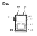
- FIG. 6C is a perspective view when the battery cell and the circuit are overlapped.
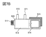
- 7A is a perspective view showing an example of the battery cell
- FIG. 7B is a perspective view of the circuit
- FIG. 7C and 7D are perspective views when the battery cell and the circuit are overlapped.
- FIG. 8 is a diagram showing a configuration example of a semiconductor device.
- FIG. 9 is a diagram showing a configuration example of a semiconductor device.
- 10A, 10B, and 10C are diagrams showing a configuration example of a semiconductor device.
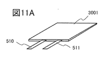
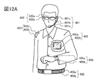
- FIG. 11A is a perspective view of the battery cell, and
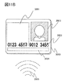
- FIG. 11B is a diagram showing an example of an electronic device.
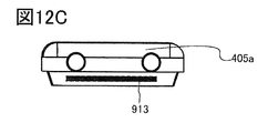
- 12A, 12B, and 12C are diagrams showing an example of an electronic device.
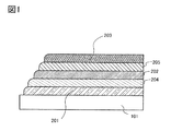
- FIG. 1 is one of the embodiments showing the case of a single-layer cell of a thin-film solid secondary battery.
- the single-layer cell of a solid secondary battery refers to a set of units having at least a positive electrode, a solid electrolyte layer, and a negative electrode.
- the single-layer cell shown in FIG. 1 is laminated on the substrate 101 in the order of the positive electrode 201, the positive electrode active material layer 204, the solid electrolyte layer 202, the negative electrode active material layer 205, and the negative electrode 203.
- the cross-sectional view shown in FIG. 1 is a part, and the plane area of the positive electrode is arranged so as to be smaller than the plane area of the negative electrode. Further, the end portion is rounded, and only one end portion is shown in FIG.
- Examples of the substrate 101 include a ceramic substrate, a glass substrate, a plastic substrate, a silicon substrate, and a metal substrate.
- the material of the positive electrode 201 and the negative electrode 203 one or more kinds of conductive materials selected from Al, Ti, Cu, Au, Cr, W, Mo, Ni, Ag and the like are used.
- a film forming method a sputtering method, a vapor deposition method or the like can be used. Further, in the sputtering method, a metal mask can be used to selectively form a film. Further, the conductive film may be patterned by selectively removing it by dry etching or wet etching using a resist mask or the like.
- the positive electrode active material layer 204 is a sputtering target containing lithium cobalt oxide (LiCoO 2 , LiCo 2 O 4, etc.) as a main component, or sputtering containing lithium manganese oxide (LiMnO 2 , LiMn 2 O 4, etc.) as a main component.
- a film can be formed by a sputtering method using a target or a lithium nickel oxide (O 2 for Li, LiNi 2 O 4 or the like).
- nickel cobalt manganese ternary material LiNi 1/3 Mn 1/3 Co 1/3 O 2 : NCM
- NiNi 1/3 Mn 1/3 Co 1/3 O 2 : NCM nickel cobalt aluminum.
- An original material LiNi 0.8 Co 0.15 Al 0.05 O 2 : NCA
- NCA nickel cobalt aluminum
- the solid electrolyte layer 202 uses a mixed material of an inorganic material and an organic material.
- a mixed material obtained by co-depositing SiO X (0 ⁇ X ⁇ 2) and an organic complex of lithium is used.
- the material to be co-deposited with SiO X (0 ⁇ X ⁇ 2) is either a simple substance of an alkali metal or an alkaline earth metal, an organic complex or a compound, and examples thereof include Li and Li 2 O. .. In particular, an organic complex of lithium is preferable, and among them, 8-hydroxyquinolinato-lithium (abbreviation: Liq) is preferable.
- Other organic materials to be co-deposited with SiO X (0 ⁇ X ⁇ 2) include dilithium phthalocyanine (dilithium phthalocyanine), lithium 2- (2-pyridyl) phenolate (abbreviation: Lipp), lithium 2- (2'). , 2''—bipyridine-6'-yl) phenolate (abbreviation: Libpp) can also be used.
- the film forming conditions it is preferable to adjust the film forming conditions so that the ratio (O / Si) of silicon and oxygen of the obtained solid electrolyte layer 202 is larger than 1 and smaller than 2. Within such a range, a solid electrolyte layer in which lithium ions are easily diffused and has no electron conductivity can be realized.
- the solid electrolyte layer 202 may have a stacked structure, when a stacked, more lithium phosphate (Li 3 PO 4) adding nitrogen to the material: the (Li 3 PO 4-Y N Y also called LiPON) It may be laminated. In addition, Y> 0.
- the negative electrode active material layer 205 is formed of a silicon-based film, a carbon-based film, a titanium oxide film, a vanadium oxide film, an indium oxide film, a zinc oxide film, a tin oxide film, or the like by using a sputtering method or the like.
- a nickel oxide film or the like can be used.
- a Li metal film may be used as the negative electrode active material layer 205.
- lithium titanium oxide Li 4 Ti 5 O 12 , LiTi 2 O 4, etc.
- FIGS. 2A and 2B An example in which the stacking order is different from that of FIG. 1 is shown in FIGS. 2A and 2B.
- FIG. 2A is a top view
- FIG. 2B corresponds to a cross-sectional view cut along the line AA'in FIG. 2A.
- a negative electrode 203 is formed on the substrate 101, and the negative electrode active material layer 205, the solid electrolyte layer 202, the positive electrode active material layer 204, the positive electrode 201, and the protective layer 206 are laminated in this order on the negative electrode 203. ing.
- the negative electrode 203, the negative electrode active material layer 205, the positive electrode active material layer 204, the positive electrode 201, and the protective layer 206 may be selectively formed by a sputtering method.
- the solid electrolyte layer 202 is selectively formed by using a co-deposited method and using a metal mask.
- the solid electrolyte layer 202 is formed by thin-filming Si powder (SiO) and Li powder and co-depositing them. For co-evaporation, a resistance heating source or an electron beam vapor deposition source is used.
- the powder is not limited to Si powder (SiO), and pellet-shaped powder may be used.
- a part of the negative electrode 203 is exposed to form a negative electrode terminal portion.
- the region other than the negative electrode terminal portion is covered with the protective layer 206.
- a part of the positive electrode 201 is exposed to form a positive electrode terminal portion.
- the region other than the positive electrode terminal portion is covered with the protective layer 206.
- a silicon nitride film (also referred to as a SiN film) is used as the protective layer 206.
- the silicon nitride film is formed by a sputtering method.
- the thin film type solid-state secondary battery shown in FIG. 2A can be manufactured by the above series of steps.
- the concentrations of silicon, nitrogen, carbon, and oxygen inside or on the surface layer of the solid electrolyte layer 202 are quantified by using EDX surface analysis (for example, element mapping). Can be analyzed.
- the solid electrolyte layer 202 was formed into a film, and the EDX measurement thereof was performed.
- the EDX spectrum of the cross section of the solid electrolyte layer 202 will be described.
- the measurement point is irradiated with an electron beam, and the energy and the number of generations of the characteristic X-rays generated by this are measured to obtain an EDX spectrum.
- Table 1 shows the percentage of atomic number concentration.
- the obtained material is a material in which lithium ions are easily diffused and has no electron conductivity, and can be used as a solid electrolyte.
- the oxygen ratio of the solid electrolyte layer can be calculated based on the value obtained by the EDX measurement.
- the ratio of silicon to oxygen (O / Si) in the solid electrolyte layer is greater than 1 and less than 2. Within such a range, it is possible to realize a solid electrolyte in which lithium ions are easily diffused and there is no electron conductivity.
- the film formation of the solid electrolyte is not limited to co-deposition, and the film formation is performed by simultaneously generating SiO gas and Li gas in the same chamber and cooling those gases on the same surface to be deposited. You can also.
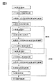
- Embodiment 2 Although an example of a single-layer cell is shown in the first embodiment, an example of a multi-layer cell is shown in the present embodiment. 4 and 5 are one of the embodiments showing the case of a multi-layer cell of a thin film type solid secondary battery.
- FIG. 4 shows an example of the cross section of the three-layer cell.
- the positive electrode 201 is formed on the substrate 101, and the positive electrode active material layer 204, the solid electrolyte layer 202, the negative electrode active material layer 205, and the negative electrode 203 are sequentially formed on the positive electrode 201 to form the first cell. There is.
- a second cell is formed by sequentially forming a second negative electrode active material layer, a second solid electrolyte layer, a second positive electrode active material layer, and a second positive electrode on the negative electrode 203. It is configured.
- a third positive electrode active material layer a third solid electrolyte layer, a third negative electrode active material layer, and a third negative electrode on the second positive electrode. It constitutes the cell of the eye.
- the protective layer 206 is finally formed.
- the three-layer stacking shown in FIG. 4 is configured to be connected in series in order to increase the capacity, but it can also be connected in parallel by an external connection. In addition, series and parallel or series-parallel can be selected for external wiring.
- the solid electrolyte layer 202, the second solid electrolyte layer, and the third solid electrolyte layer are preferable because the production cost can be reduced by using the same material.
- FIG. 4 An example of a manufacturing flow for obtaining the structure shown in FIG. 4 is shown in FIG.
- an LCO film is used as the positive electrode active material layer, a titanium film is used as the current collector, and the titanium film is regarded as the positive electrode. Further, a silicon film is used as the negative electrode active material layer, and a titanium film is used as the current collector, which is regarded as the negative electrode.
- a titanium film is used as a common electrode, a three-layer laminated cell is realized with a small number of configurations.
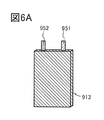
- FIG. 6A is an external view of a thin film type solid-state secondary battery.
- the secondary battery 913 has a terminal 951 and a terminal 952.
- the terminal 951 is electrically connected to the positive electrode and the terminal 952 is electrically connected to the negative electrode.
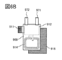
- FIG. 6B is an external view of the battery control circuit.
- the battery control circuit shown in FIG. 6B has a substrate 900 and layer 916.
- a circuit 912 and an antenna 914 are provided on the substrate 900.
- the antenna 914 is electrically connected to the circuit 912.
- Terminals 971 and 972 are electrically connected to the circuit 912.
- the circuit 912 is electrically connected to the terminal 911.
- the terminal 911 is connected to, for example, a device to which power is supplied from a thin-film solid-state secondary battery. For example, it is connected to a display device, a sensor, or the like.
- the layer 916 has a function capable of shielding the electromagnetic field generated by the secondary battery 913, for example.
- a magnetic material can be used as the layer 916.
- FIG. 6C shows an example in which the battery control circuit shown in FIG. 6B is arranged on the secondary battery 913.
- the terminal 971 is electrically connected to the terminal 951, and the terminal 972 is electrically connected to the terminal 952.
- Layer 916 is arranged between the substrate 900 and the secondary battery 913.
- a flexible substrate as the substrate 900.
- a thin battery control circuit can be realized. Further, as shown in FIG. 7D described later, the battery control circuit can be wound around the secondary battery.
- FIG. 7A is an external view of a thin film type solid-state secondary battery.
- the battery control circuit shown in FIG. 7B has a substrate 900 and layer 916.
- the substrate 900 is bent according to the shape of the secondary battery 913, and the battery control circuit is arranged around the secondary battery, so that the battery control circuit is changed to the secondary battery as shown in FIG. 7D. Can be wrapped around.
- Embodiment 4 a transistor configuration applicable to the battery control circuit described in the above embodiment will be described. Specifically, a configuration in which transistors having different electrical characteristics are laminated and provided will be described. With this configuration, the degree of freedom in designing the semiconductor device can be increased. Further, by stacking transistors having different electrical characteristics, the degree of integration of the semiconductor device can be increased.
- the semiconductor device shown in FIG. 8 has a transistor 300, a transistor 500, and a capacity of 600.
- 10A is a cross-sectional view of the transistor 500 in the channel length direction
- FIG. 10B is a cross-sectional view of the transistor 500 in the channel width direction
- FIG. 10C is a cross-sectional view of the transistor 300 in the channel width direction.
- the transistor 500 is an OS transistor. Therefore, since the transistor 500 has an extremely small off current, it is possible to retain the data voltage or electric charge written for a long period of time by using the transistor 500 for a transistor included in the semiconductor device. That is, since the frequency of the refresh operation is low or the refresh operation is not required, the power consumption of the semiconductor device can be reduced.
- the semiconductor device described in the present embodiment has a transistor 300, a transistor 500, and a capacity of 600.
- the transistor 500 is provided above the transistor 300
- the capacitance 600 is provided above the transistor 300 and the transistor 500.
- the transistor 300 is provided on the substrate 311 and has a semiconductor region 313 composed of a conductor 316, an insulator 315, and a part of the substrate 311, a low resistance region 314a functioning as a source region or a drain region, and a low resistance region 314b. ..
- the transistor 300 is covered with the conductor 316 on the upper surface of the semiconductor region 313 and the side surface in the channel width direction via the insulator 315.
- the on-characteristics of the transistor 300 can be improved by increasing the effective channel width. Further, since the contribution of the electric field of the gate electrode can be increased, the off characteristic of the transistor 300 can be improved.
- the transistor 300 may be either a p-channel type or an n-channel type.
- a semiconductor such as a silicon-based semiconductor is included in a region in which a channel of the semiconductor region 313 is formed, a region in the vicinity thereof, a low resistance region 314a serving as a source region or a drain region, a low resistance region 314b, and the like. It preferably contains crystalline silicon. Alternatively, it may be formed of a material having Ge (germanium), SiGe (silicon germanium), GaAs (gallium arsenide), GaAlAs (gallium aluminum arsenide), or the like. A configuration using silicon in which the effective mass is controlled by applying stress to the crystal lattice and changing the lattice spacing may be used. Alternatively, the transistor 300 may be a HEMT (High Electron Mobility Transistor) by using GaAs, GaAlAs, or the like.
- HEMT High Electron Mobility Transistor
- the low resistance region 314a and the low resistance region 314b impart n-type conductivity-imparting elements such as arsenic and phosphorus, or p-type conductivity such as boron, in addition to the semiconductor material applied to the semiconductor region 313. Contains elements that
- the conductor 316 that functions as a gate electrode is a semiconductor material such as silicon, a metal material, or an alloy that contains an element that imparts n-type conductivity such as arsenic or phosphorus, or an element that imparts p-type conductivity such as boron.
- a material or a conductive material such as a metal oxide material can be used.
- the threshold voltage of the transistor can be adjusted by selecting the material of the conductor. Specifically, it is preferable to use a material such as titanium nitride or tantalum nitride for the conductor. Further, in order to achieve both conductivity and embedding property, it is preferable to use a metal material such as tungsten or aluminum as a laminate for the conductor, and it is particularly preferable to use tungsten in terms of heat resistance.
- the transistor 300 shown in FIG. 8 is an example, and the transistor 300 is not limited to the structure thereof, and an appropriate transistor may be used according to the circuit configuration and the driving method.
- the semiconductor device is a unipolar circuit containing only OS transistors (meaning transistors having the same polarity as n-channel transistors only, etc.)
- the transistor 300 is configured by using an oxide semiconductor.
- the configuration may be the same as that of the transistor 500. The details of the transistor 500 will be described later.
- An insulator 320, an insulator 322, an insulator 324, and an insulator 326 are laminated in this order so as to cover the transistor 300.
- the insulator 320, the insulator 322, the insulator 324, and the insulator 326 for example, silicon oxide, silicon oxide, silicon nitride, silicon nitride, aluminum oxide, aluminum oxide, aluminum nitride, aluminum nitride and the like can be used. Just do it.
- silicon oxide refers to a material whose composition has a higher oxygen content than nitrogen
- silicon nitride refers to a material whose composition has a higher nitrogen content than oxygen. Is shown.
- aluminum nitride refers to a material whose composition has a higher oxygen content than nitrogen
- aluminum nitride refers to a material whose composition has a higher nitrogen content than oxygen. Is shown.
- the insulator 322 may have a function as a flattening film for flattening a step generated by a transistor 300 or the like provided below the insulator 322.
- the upper surface of the insulator 322 may be flattened by a flattening treatment using a chemical mechanical polishing (CMP) method or the like in order to improve the flatness.
- CMP chemical mechanical polishing
- the insulator 324 it is preferable to use a film having a barrier property so that hydrogen and impurities do not diffuse in the region where the transistor 500 is provided from the substrate 311 or the transistor 300.
- a film having a barrier property against hydrogen for example, silicon nitride formed by the CVD method can be used.
- hydrogen may diffuse into a semiconductor element having an oxide semiconductor such as a transistor 500, so that the characteristics of the semiconductor element may deteriorate. Therefore, it is preferable to use a film that suppresses the diffusion of hydrogen between the transistor 500 and the transistor 300.
- the membrane that suppresses the diffusion of hydrogen is a membrane that desorbs a small amount of hydrogen.
- the amount of hydrogen desorbed can be analyzed using, for example, a heated desorption gas analysis method (TDS).
- TDS heated desorption gas analysis method
- the amount of hydrogen desorbed from the insulator 324 is such that the amount desorbed in terms of hydrogen atoms is converted per area of the insulator 324 when the surface temperature of the film is in the range of 50 ° C. to 500 ° C. It may be 10 ⁇ 10 15 atoms / cm 2 or less, preferably 5 ⁇ 10 15 atoms / cm 2 or less.
- the insulator 326 preferably has a lower dielectric constant than the insulator 324.
- the relative permittivity of the insulator 326 is preferably less than 4, more preferably less than 3.
- the relative permittivity of the insulator 326 is preferably 0.7 times or less, more preferably 0.6 times or less, the relative permittivity of the insulator 324.
- the insulator 320, the insulator 322, the insulator 324, and the insulator 326 are embedded with a capacity of 600, a conductor 328 connected to the transistor 500, a conductor 330, and the like.
- the conductor 328 and the conductor 330 have a function as a plug or a wiring.
- a conductor having a function as a plug or a wiring may collectively give a plurality of structures the same reference numerals.
- the wiring and the plug connected to the wiring may be integrated. That is, a part of the conductor may function as a wiring, and a part of the conductor may function as a plug.
- each plug and wiring As the material of each plug and wiring (conductor 328, conductor 330, etc.), a conductive material such as a metal material, an alloy material, a metal nitride material, or a metal oxide material is used as a single layer or laminated. be able to. It is preferable to use a refractory material such as tungsten or molybdenum that has both heat resistance and conductivity, and it is preferable to use tungsten. Alternatively, it is preferably formed of a low resistance conductive material such as aluminum or copper. Wiring resistance can be reduced by using a low resistance conductive material.
- a wiring layer may be provided on the insulator 326 and the conductor 330.
- the insulator 350, the insulator 352, and the insulator 354 are laminated in this order.
- a conductor 356 is formed on the insulator 350, the insulator 352, and the insulator 354.
- the conductor 356 has a function as a plug or wiring for connecting to the transistor 300.
- the conductor 356 can be provided by using the same materials as the conductor 328 and the conductor 330.
- the insulator 350 it is preferable to use an insulator having a barrier property against hydrogen, similarly to the insulator 324.
- the conductor 356 preferably contains a conductor having a barrier property against hydrogen.
- a conductor having a barrier property against hydrogen is formed in the opening of the insulator 350 having a barrier property against hydrogen.
- the conductor having a barrier property against hydrogen for example, tantalum nitride or the like may be used. Further, by laminating tantalum nitride and tungsten having high conductivity, it is possible to suppress the diffusion of hydrogen from the transistor 300 while maintaining the conductivity as wiring. In this case, it is preferable that the tantalum nitride layer having a barrier property against hydrogen has a structure in contact with the insulator 350 having a barrier property against hydrogen.
- a wiring layer may be provided on the insulator 354 and the conductor 356.
- the insulator 360, the insulator 362, and the insulator 364 are laminated in this order.
- a conductor 366 is formed on the insulator 360, the insulator 362, and the insulator 364.
- the conductor 366 has a function as a plug or wiring.
- the conductor 366 can be provided by using the same materials as the conductor 328 and the conductor 330.
- the insulator 360 it is preferable to use an insulator having a barrier property against hydrogen, similarly to the insulator 324.
- the conductor 366 preferably contains a conductor having a barrier property against hydrogen.
- a conductor having a barrier property against hydrogen is formed in the opening of the insulator 360 having a barrier property against hydrogen.
- a wiring layer may be provided on the insulator 364 and the conductor 366.
- the insulator 370, the insulator 372, and the insulator 374 are laminated in this order.
- a conductor 376 is formed on the insulator 370, the insulator 372, and the insulator 374.
- the conductor 376 has a function as a plug or wiring.
- the conductor 376 can be provided by using the same material as the conductor 328 and the conductor 330.
- the insulator 370 it is preferable to use an insulator having a barrier property against hydrogen, similarly to the insulator 324.
- the conductor 376 preferably contains a conductor having a barrier property against hydrogen.
- a conductor having a barrier property against hydrogen is formed in the opening of the insulator 370 having a barrier property against hydrogen.
- a wiring layer may be provided on the insulator 374 and the conductor 376.
- the insulator 380, the insulator 382, and the insulator 384 are laminated in this order.
- a conductor 386 is formed on the insulator 380, the insulator 382, and the insulator 384.
- the conductor 386 has a function as a plug or wiring.
- the conductor 386 can be provided by using the same materials as the conductor 328 and the conductor 330.
- the insulator 380 it is preferable to use an insulator having a barrier property against hydrogen, similarly to the insulator 324.
- the conductor 386 preferably contains a conductor having a barrier property against hydrogen.
- a conductor having a barrier property against hydrogen is formed in the opening of the insulator 380 having a barrier property against hydrogen.
- the semiconductor device according to the present embodiment has been described. It is not limited to this.
- the number of wiring layers similar to the wiring layer including the conductor 356 may be 3 or less, or the number of wiring layers similar to the wiring layer including the conductor 356 may be 5 or more.
- the insulator 510, the insulator 512, the insulator 514, and the insulator 516 are laminated in this order.
- the insulator 510, the insulator 512, the insulator 514, and the insulator 516 it is preferable to use a substance having a barrier property against oxygen and hydrogen.
- a film having a barrier property so that hydrogen and impurities do not diffuse from the area where the substrate 311 or the transistor 300 is provided to the area where the transistor 500 is provided is used. Is preferable. Therefore, the same material as the insulator 324 can be used.
- Silicon nitride formed by the CVD method can be used as an example of a film having a barrier property against hydrogen.
- hydrogen may diffuse into a semiconductor element having an oxide semiconductor such as a transistor 500, so that the characteristics of the semiconductor element may deteriorate. Therefore, it is preferable to use a film that suppresses the diffusion of hydrogen between the transistor 500 and the transistor 300.
- the membrane that suppresses the diffusion of hydrogen is a membrane that desorbs a small amount of hydrogen.
- the film having a barrier property against hydrogen for example, it is preferable to use metal oxides such as aluminum oxide, hafnium oxide, and tantalum oxide for the insulator 510 and the insulator 514.
- metal oxides such as aluminum oxide, hafnium oxide, and tantalum oxide for the insulator 510 and the insulator 514.
- aluminum oxide has a high blocking effect that does not allow the membrane to permeate both oxygen and impurities such as hydrogen and water that cause fluctuations in the electrical characteristics of the transistor. Therefore, aluminum oxide can prevent impurities such as hydrogen and moisture from being mixed into the transistor 500 during and after the manufacturing process of the transistor. In addition, the release of oxygen from the oxides constituting the transistor 500 can be suppressed. Therefore, it is suitable for use as a protective film for the transistor 500.
- the same material as that of the insulator 320 can be used for the insulator 512 and the insulator 516. Further, by applying a material having a relatively low dielectric constant to these insulators, it is possible to reduce the parasitic capacitance generated between the wirings.
- a silicon oxide film, a silicon nitride film, or the like can be used as the insulator 512 and the insulator 516.
- a conductor 518 a conductor constituting the transistor 500 (for example, a conductor 503) and the like are embedded.
- the conductor 518 has a function as a capacity 600, a plug for connecting to the transistor 300, or wiring.
- the conductor 518 can be provided by using the same material as the conductor 328 and the conductor 330.
- the conductor 510 in the region in contact with the insulator 510 and the insulator 514 is preferably a conductor having a barrier property against oxygen, hydrogen, and water.
- the transistor 300 and the transistor 500 can be separated by a layer having a barrier property against oxygen, hydrogen, and water, and the diffusion of hydrogen from the transistor 300 to the transistor 500 can be suppressed.
- a transistor 500 is provided above the insulator 516.
- the transistor 500 includes a conductor 503 arranged so as to be embedded in the insulator 514 and the insulator 516, and an insulator 520 arranged on the insulator 516 and the insulator 503. And on the insulator 522 placed on the insulator 520, the insulator 524 placed on the insulator 522, the oxide 530a placed on the insulator 524, and the oxide 530a.
- the arranged oxide 530b, the conductors 542a and 542b arranged apart from each other on the oxide 530b, the conductors 542a and the conductors 542b, and between the conductors 542a and 542b.
- the insulator 544 is arranged between the oxide 530a, the oxide 530b, the conductor 542a, and the conductor 542b and the insulator 580.
- the conductor 560 includes a conductor 560a provided inside the insulator 550 and a conductor 560b provided so as to be embedded inside the conductor 560a. It is preferable to have.
- the insulator 574 is arranged on the insulator 580, the conductor 560, and the insulator 550.
- oxide 530a, oxide 530b, and oxide 530c may be collectively referred to as oxide 530.
- the transistor 500 a configuration in which three layers of oxide 530a, oxide 530b, and oxide 530c are laminated is shown in a region where a channel is formed and in the vicinity thereof, but the present invention is limited to this. It's not a thing.
- a single layer of oxide 530b, a two-layer structure of oxide 530b and oxide 530a, a two-layer structure of oxide 530b and oxide 530c, or a laminated structure of four or more layers may be provided.
- the conductor 560 is shown as a two-layer laminated structure, but the present invention is not limited to this.
- the conductor 560 may have a single-layer structure or a laminated structure of three or more layers.
- the transistor 500 shown in FIGS. 8 and 10A is an example, and the transistor 500 is not limited to the structure thereof, and an appropriate transistor may be used according to the circuit configuration and the driving method.
- the conductor 560 functions as a gate electrode of the transistor, and the conductor 542a and the conductor 542b function as a source electrode or a drain electrode, respectively.
- the conductor 560 is formed so as to be embedded in the opening of the insulator 580 and the region sandwiched between the conductor 542a and the conductor 542b.
- the arrangement of the conductor 560, the conductor 542a and the conductor 542b is self-aligned with respect to the opening of the insulator 580. That is, in the transistor 500, the gate electrode can be arranged in a self-aligned manner between the source electrode and the drain electrode. Therefore, since the conductor 560 can be formed without providing the alignment margin, the occupied area of the transistor 500 can be reduced. As a result, the semiconductor device can be miniaturized and highly integrated.
- the conductor 560 is formed in a region between the conductor 542a and the conductor 542b in a self-aligned manner, the conductor 560 does not have a region that overlaps with the conductor 542a or the conductor 542b. Thereby, the parasitic capacitance formed between the conductor 560 and the conductors 542a and 542b can be reduced. Therefore, the switching speed of the transistor 500 can be improved and a high frequency characteristic can be provided.
- the conductor 560 may function as a first gate (also referred to as a top gate) electrode. Further, the conductor 503 may function as a second gate (also referred to as a bottom gate) electrode.
- the threshold voltage of the transistor 500 can be controlled by changing the potential applied to the conductor 503 independently of the potential applied to the conductor 560 without interlocking with it. In particular, by applying a negative potential to the conductor 503, the threshold voltage of the transistor 500 can be made larger than 0 V, and the off-current can be reduced. Therefore, when a negative potential is applied to the conductor 503, the drain current when the potential applied to the conductor 560 is 0 V can be made smaller than when it is not applied.
- the conductor 503 is arranged so as to overlap the oxide 530 and the conductor 560. As a result, when a potential is applied to the conductor 560 and the conductor 503, the electric field generated from the conductor 560 and the electric field generated from the conductor 503 are connected to cover the channel forming region formed in the oxide 530. Can be done.
- the structure of the transistor that electrically surrounds the channel formation region by the electric field of the pair of gate electrodes is referred to as a surroundd channel (S-channel) structure.
- S-channel surroundd channel
- the side surface and the periphery of the oxide 530 in contact with the conductor 542a and the conductor 542b that function as the source electrode and the drain electrode are the same as the channel forming region. It has the characteristic of being a mold.
- the side surface and the periphery of the oxide 530 in contact with the conductor 542a and the conductor 542b are in contact with the insulator 544, it can be type I as in the channel forming region.
- type I can be treated as the same as high-purity authenticity described later.
- the S-channel structure disclosed in the present specification and the like is different from the Fin type structure and the planar type structure. By adopting the S-channel structure, it is possible to increase the resistance to the short-channel effect, in other words, to make a transistor in which the short-channel effect is unlikely to occur.
- the conductor 503 has the same structure as the conductor 518, and the conductor 503a is formed in contact with the inner walls of the openings of the insulator 514 and the insulator 516, and the conductor 503b is further formed inside.
- the transistor 500 shows a configuration in which the conductor 503a and the conductor 503b are laminated, but the present invention is not limited to this.
- the conductor 503 may be provided as a single layer or a laminated structure having three or more layers.
- the conductor 503a it is preferable to use a conductive material having a function of suppressing the diffusion of impurities such as hydrogen atoms, hydrogen molecules, water molecules, and copper atoms (the above impurities are difficult to permeate).
- a conductive material having a function of suppressing the diffusion of oxygen for example, at least one oxygen atom, oxygen molecule, etc.
- the function of suppressing the diffusion of impurities or oxygen is a function of suppressing the diffusion of any one or all of the above impurities or the above oxygen.
- the conductor 503a since the conductor 503a has a function of suppressing the diffusion of oxygen, it is possible to prevent the conductor 503b from being oxidized and the conductivity from being lowered.
- the conductor 503 When the conductor 503 also functions as a wiring, it is preferable to use a highly conductive conductive material containing tungsten, copper, or aluminum as a main component for the conductor 503b.
- the conductor 503 is shown by laminating the conductor 503a and the conductor 503b, but the conductor 503 may have a single-layer structure.
- the insulator 520, the insulator 522, and the insulator 524 have a function as a second gate insulating film.
- the insulator 524 in contact with the oxide 530 it is preferable to use an insulator containing more oxygen than oxygen satisfying the stoichiometric composition. That is, it is preferable that the insulator 524 is formed with an excess oxygen region.
- oxygen vacancies in the oxide 530 V O: oxygen vacancy also called
- the defective hereinafter sometimes referred to as V O H.
- the defective Functions as a donor, sometimes electrons serving as carriers are generated.
- a part of hydrogen may be combined with oxygen that is bonded to a metal atom to generate an electron as a carrier. Therefore, a transistor using an oxide semiconductor containing a large amount of hydrogen tends to have a normally-on characteristic. Further, since hydrogen in the oxide semiconductor easily moves due to stress such as heat and electric field, if the oxide semiconductor contains a large amount of hydrogen, the reliability of the transistor may deteriorate. In one aspect of the present invention to reduce as much as possible V O H in the oxide 530, it is preferable that the highly purified intrinsic or substantially highly purified intrinsic.
- the V O H to obtain a sufficiently reduced oxide semiconductor the moisture in the oxide semiconductor, to remove impurities such as hydrogen (dehydration, may be described as dehydrogenation.) It is important to supply oxygen to the oxide semiconductor to compensate for the oxygen deficiency (sometimes referred to as dehydrogenation treatment).
- the V O H oxide semiconductor impurity is sufficiently reduced such by using a channel formation region of the transistor, it is possible to have stable electrical characteristics.
- an oxide material in which a part of oxygen is desorbed by heating is 1.0 ⁇ 10 18 atoms / cm 3 or more, preferably 1 in TDS (Thermal Desorption Spectroscopy) analysis.
- the surface temperature of the film during the TDS analysis is preferably in the range of 100 ° C. or higher and 700 ° C. or lower, or 100 ° C. or higher and 400 ° C. or lower.
- the insulator having the excess oxygen region and the oxide 530 may be brought into contact with each other to perform one or more of heat treatment, microwave treatment, or RF treatment.
- heat treatment microwave treatment, or RF treatment.
- water or hydrogen in the oxide 530 can be removed.
- reactions occur which bonds VoH is disconnected, when other words happening reaction of "V O H ⁇ Vo + H", it can be dehydrogenated.
- the hydrogen generated as oxygen combines with H 2 O, it may be removed from the oxide 530 or oxide 530 near the insulator.
- a part of hydrogen may be gettered on the conductor 542.
- the microwave processing for example, it is preferable to use an apparatus having a power source for generating high-density plasma or an apparatus having a power source for applying RF to the substrate side.
- an apparatus having a power source for generating high-density plasma for example, by using a gas containing oxygen and using a high-density plasma, high-density oxygen radicals can be generated, and by applying RF to the substrate side, the oxygen radicals generated by the high-density plasma can be generated.
- the pressure may be 133 Pa or more, preferably 200 Pa or more, and more preferably 400 Pa or more.
- oxygen and argon are used as the gas to be introduced into the apparatus for performing microwave treatment, and the oxygen flow rate ratio (O 2 / (O 2 + Ar)) is 50% or less, preferably 10% or more and 30. It is recommended to use less than%.
- the heat treatment may be performed, for example, at 100 ° C. or higher and 450 ° C. or lower, more preferably 350 ° C. or higher and 400 ° C. or lower.
- the heat treatment is carried out in an atmosphere of nitrogen gas or an inert gas, or an atmosphere containing 10 ppm or more, 1% or more, or 10% or more of an oxidizing gas.
- the heat treatment is preferably performed in an oxygen atmosphere.
- oxygen can be supplied to the oxide 530 to reduce oxygen deficiency ( VO ).
- the heat treatment may be performed in a reduced pressure state.
- the heat treatment may be carried out in an atmosphere containing 10 ppm or more, 1% or more, or 10% or more of oxidizing gas in order to supplement the desorbed oxygen after the heat treatment in an atmosphere of nitrogen gas or an inert gas.
- the heat treatment may be performed in an atmosphere containing 10 ppm or more, 1% or more, or 10% or more of the oxidizing gas, and then the heat treatment may be continuously performed in an atmosphere of nitrogen gas or an inert gas.
- the oxygen deficiency in the oxide 530 can be repaired by the supplied oxygen, in other words, the reaction "Vo + O ⁇ null" can be promoted. Further, since the oxygen supplied to the hydrogen remaining in the oxide 530 is reacted to remove the hydrogen as H 2 O (to dehydration) can. Thus, the hydrogen remained in the oxide 530 can be prevented from recombine V O H is formed by oxygen vacancies.
- the insulator 524 has an excess oxygen region, it is preferable that the insulator 522 has a function of suppressing the diffusion of oxygen (for example, oxygen atom, oxygen molecule, etc.) (the oxygen is difficult to permeate).
- oxygen for example, oxygen atom, oxygen molecule, etc.
- the insulator 522 has a function of suppressing the diffusion of oxygen and impurities, the oxygen contained in the oxide 530 does not diffuse to the insulator 520 side, which is preferable. Further, it is possible to suppress the conductor 503 from reacting with the oxygen contained in the insulator 524 and the oxide 530.
- the insulator 522 may be, for example, aluminum oxide, hafnium oxide, an oxide containing aluminum and hafnium (hafnium aluminate), tantalum oxide, zirconium oxide, lead zirconate titanate (PZT), strontium titanate (SrTIO 3 ), or It is preferable to use an insulator containing a so-called high-k material such as (Ba, Sr) TiO 3 (BST) in a single layer or in a laminated manner. As the miniaturization and high integration of transistors progress, problems such as leakage current may occur due to the thinning of the gate insulating film. By using a high-k material for the insulator that functions as a gate insulating film, it is possible to reduce the gate potential during transistor operation while maintaining the physical film thickness.
- a so-called high-k material such as (Ba, Sr) TiO 3 (BST)
- an insulator containing an oxide of one or both of aluminum and hafnium which are insulating materials having a function of suppressing diffusion of impurities and oxygen (the above-mentioned oxygen is difficult to permeate).
- the insulator containing one or both oxides of aluminum and hafnium it is preferable to use aluminum oxide, hafnium oxide, an oxide containing aluminum and hafnium (hafnium aluminate) and the like.
- the insulator 522 is formed by using such a material, the insulator 522 suppresses the release of oxygen from the oxide 530 and the mixing of impurities such as hydrogen from the peripheral portion of the transistor 500 into the oxide 530. Acts as a layer.
- aluminum oxide, bismuth oxide, germanium oxide, niobium oxide, silicon oxide, titanium oxide, tungsten oxide, yttrium oxide, and zirconium oxide may be added to these insulators.
- these insulators may be nitrided. Silicon oxide, silicon oxide or silicon nitride may be laminated on the above insulator.
- the insulator 520 is preferably thermally stable.
- silicon oxide and silicon oxide nitride are suitable because they are thermally stable.
- an insulator 520 having a laminated structure that is thermally stable and has a high relative permittivity can be obtained.
- oxide 530 a metal oxide that functions as an oxide semiconductor for the oxide 530 containing the channel forming region.
- oxide 530 In-M-Zn oxide (element M is aluminum, gallium, yttrium, copper, vanadium, beryllium, boron, titanium, iron, nickel, germanium, zirconium, molybdenum, lantern, cerium, neodymium). , Hafnium, tantalum, tungsten, magnesium, etc. (one or more) and the like may be used.
- the In-M-Zn oxide that can be applied as the oxide 530 is preferably CAAC-OS (c-axis aligned crystalline oxide semiconductor).
- CAC-OS Cloud-Aligned Complex oxide semiconductor
- CAAC represents an example of a crystal structure
- CAC represents an example of a function or a composition of a material.
- CAC-OS has a conductive function in a part of the material and an insulating function in a part of the material, and has a function as a semiconductor in the whole material.
- the conductive function is the function of flowing electrons (or holes) that serve as carriers
- the insulating function is the function of flowing electrons (or holes) that serve as carriers. It is a function that does not shed.
- CAC-OS or CAC-metal oxide has a conductive region and an insulating region.
- the conductive region has the above-mentioned conductive function
- the insulating region has the above-mentioned insulating function.
- the conductive region and the insulating region may be separated at the nanoparticle level. Further, the conductive region and the insulating region may be unevenly distributed in the material. In addition, the conductive region may be observed with the periphery blurred and connected in a cloud shape.
- CAC-OS or CAC-metal oxide when the conductive region and the insulating region are dispersed in the material in a size of 0.5 nm or more and 10 nm or less, preferably 0.5 nm or more and 3 nm or less, respectively. There is.
- CAC-OS or CAC-metal oxide is composed of components having different band gaps.
- CAC-OS or CAC-metal oxide is composed of a component having a wide gap due to an insulating region and a component having a narrow gap due to a conductive region.
- the carriers when the carriers flow, the carriers mainly flow in the components having a narrow gap.
- the component having a narrow gap acts complementarily to the component having a wide gap, and the carrier flows to the component having a wide gap in conjunction with the component having a narrow gap. Therefore, when the CAC-OS or CAC-metal oxide is used in the channel formation region of the transistor, a high current driving force, that is, a large on-current and a high field effect mobility can be obtained in the ON state of the transistor.
- CAC-OS or CAC-metal composite can also be referred to as a matrix composite material (matrix composite) or a metal matrix composite material (metal matrix composite).
- the metal oxide that functions as an oxide semiconductor is divided into a single crystal oxide semiconductor and other non-single crystal oxide semiconductors.
- the non-monocrystalline oxide semiconductor include CAAC-OS, polycrystalline oxide semiconductor, nc-OS (nanocrystalline oxide semiconductor), pseudo-amorphous oxide semiconductor (a-like OS: amorphous-like oxide semiconductor), and the like. And amorphous oxide semiconductors.
- IGZO is roughly classified into Amorphous (amorphous), Crystalline (crystallinity), and Crystal (crystal).
- Amorphous includes complete amorphous.
- the Crystalline includes CAAC (c-axis aligned crystalline), nc (nanocrystalline), and CAC (Cloud-Aligned Composite).
- single crystal, poly crystal, and single crystal amorphous are excluded from the classification of Crystal line.
- Crystal includes single crystal and poly crystal.
- CAAC-OS has a c-axis orientation and has a distorted crystal structure in which a plurality of nanocrystals are connected in the ab plane direction.
- the strain refers to a region in which a plurality of nanocrystals are connected, in which the orientation of the lattice arrangement changes between a region in which the lattice arrangement is aligned and a region in which another lattice arrangement is aligned.
- nanocrystals are basically hexagonal, they are not limited to regular hexagons and may have non-regular hexagons. In addition, it may have a lattice arrangement such as a pentagon and a heptagon in distortion.
- a lattice arrangement such as a pentagon and a heptagon in distortion.
- CAAC-OS it is difficult to confirm a clear grain boundary (also referred to as grain boundary) even in the vicinity of strain. That is, it can be seen that the formation of grain boundaries is suppressed by the distortion of the lattice arrangement. This is because the CAAC-OS can tolerate distortion because the arrangement of oxygen atoms is not dense in the ab plane direction and the bond distance between atoms changes due to the substitution of metal elements. Because.
- CAAC-OS is a layered crystal in which a layer having indium and oxygen (hereinafter, In layer) and a layer having elements M, zinc, and oxygen (hereinafter, (M, Zn) layer) are laminated. It tends to have a structure (also called a layered structure). Indium and the element M can be replaced with each other, and when the element M of the (M, Zn) layer is replaced with indium, it can be expressed as the (In, M, Zn) layer. Further, when the indium of the In layer is replaced with the element M, it can be expressed as the (In, M) layer.
- CAAC-OS is a highly crystalline metal oxide.
- CAAC-OS it is difficult to confirm a clear grain boundary, so it can be said that a decrease in electron mobility due to the crystal grain boundary is unlikely to occur.
- CAAC-OS since the crystallinity of the metal oxide may be lowered due to the mixing of impurities or the formation of defects, CAAC-OS can be said to be a metal oxide having few impurities and defects (oxygen deficiency, etc.). Therefore, the metal oxide having CAAC-OS has stable physical properties. Therefore, the metal oxide having CAAC-OS is resistant to heat and has high reliability.
- the nc-OS has periodicity in the atomic arrangement in a minute region (for example, a region of 1 nm or more and 10 nm or less, particularly a region of 1 nm or more and 3 nm or less).
- nc-OS does not show regularity in crystal orientation between different nanocrystals. Therefore, no orientation is observed in the entire film. Therefore, nc-OS may be indistinguishable from a-like OS and amorphous oxide semiconductors depending on the analysis method.
- In-Ga-Zn oxide (also referred to as "IGZO"), which is a kind of metal oxide having indium, gallium, and zinc, has a stable structure by forming the above-mentioned nanocrystals. May be taken.
- IGZO tends to have difficulty in crystal growth in the atmosphere, it is preferable to use smaller crystals (for example, the above-mentioned nanocrystals) than large crystals (here, a few mm crystal or a few cm crystal). However, it may be structurally stable.
- the a-like OS is a metal oxide having a structure between the nc-OS and an amorphous oxide semiconductor.
- the a-like OS has a void or low density region. That is, the a-like OS has lower crystallinity than the nc-OS and CAAC-OS.
- Oxide semiconductors have various structures, and each has different characteristics.
- the oxide semiconductor of one aspect of the present invention may have two or more of amorphous oxide semiconductor, polycrystalline oxide semiconductor, a-like OS, nc-OS, and CAAC-OS.
- a metal oxide having a low carrier concentration for the transistor 500 it is preferable to use a metal oxide having a low carrier concentration for the transistor 500.
- the impurity concentration in the metal oxide may be lowered to lower the defect level density.
- a low impurity concentration and a low defect level density is referred to as high-purity intrinsic or substantially high-purity intrinsic.
- impurities in the metal oxide include hydrogen, nitrogen, alkali metal, alkaline earth metal, iron, nickel, silicon and the like.
- hydrogen contained in a metal oxide reacts with oxygen bonded to a metal atom to form water, which may form an oxygen deficiency in the metal oxide. If the channel forming region in the metal oxide contains oxygen deficiency, the transistor may have a normally-on characteristic.
- a defect containing hydrogen in an oxygen deficiency may function as a donor and generate electrons as carriers.
- a part of hydrogen may be combined with oxygen that is bonded to a metal atom to generate an electron as a carrier. Therefore, a transistor using a metal oxide containing a large amount of hydrogen tends to have a normally-on characteristic.
- Defects containing hydrogen in oxygen deficiencies can function as donors for metal oxides. However, it is difficult to quantitatively evaluate the defect. Therefore, in the case of metal oxides, the carrier concentration may be used instead of the donor concentration. Therefore, in the present specification and the like, as a parameter of the metal oxide, a carrier concentration assuming a state in which an electric field is not applied may be used instead of the donor concentration. That is, the "carrier concentration" described in the present specification and the like may be paraphrased as the "donor concentration".
- the hydrogen concentration obtained by secondary ion mass spectrometry is less than 1 ⁇ 10 20 atoms / cm 3 , preferably 1 ⁇ 10 19 atoms / cm. It is less than 3 , more preferably less than 5 ⁇ 10 18 atoms / cm 3 , and even more preferably less than 1 ⁇ 10 18 atoms / cm 3 .
- the carrier concentration of the metal oxide in the channel formation region is preferably 1 ⁇ 10 18 cm -3 or less, and preferably less than 1 ⁇ 10 17 cm -3. Is more preferably less than 1 ⁇ 10 16 cm -3 , even more preferably less than 1 ⁇ 10 13 cm -3 , even more preferably less than 1 ⁇ 10 12 cm -3 .
- the lower limit of the carrier concentration of the metal oxide in the channel formation region is not particularly limited, but may be, for example, 1 ⁇ 10 -9 cm -3 .
- the oxygen in the oxide 530 diffuses to the conductor 542 when the conductor 542 (conductor 542a and the conductor 542b) and the oxide 530 come into contact with each other.
- the conductor 542 may oxidize. It is highly probable that the conductivity of the conductor 542 will decrease due to the oxidation of the conductor 542.
- the diffusion of oxygen in the oxide 530 into the conductor 542 can be rephrased as the conductor 542 absorbing the oxygen in the oxide 530.
- oxygen in the oxide 530 diffuses into the conductor 542 (conductor 542a and the conductor 542b), so that the oxygen in the oxide 530 diffuses between the conductor 542a and the oxide 530b, and the conductor 542b and the oxide 530b.
- Different layers may be formed between them. Since the different layer contains more oxygen than the conductor 542, it is presumed that the different layer has an insulating property.
- the three-layer structure of the conductor 542, the different layer, and the oxide 530b can be regarded as a three-layer structure composed of a metal, an insulator, and a semiconductor, and can be regarded as a MIS (Metal-Insulator-Semiconductor) structure. It may be called, or it may be called a diode junction structure mainly composed of a MIS structure.
- the different layer is not limited to being formed between the conductor 542 and the oxide 530b.
- the different layer is formed between the conductor 542 and the oxide 530c, or when the different layer is conductive. It may be formed between the body 542 and the oxide 530b, and between the conductor 542 and the oxide 530c.
- a metal oxide having a band gap of 2 eV or more, preferably 2.5 eV or more, which functions as a channel forming region in the oxide 530 it is preferable to use a metal oxide having a band gap of 2 eV or more, preferably 2.5 eV or more, which functions as a channel forming region in the oxide 530. As described above, by using a metal oxide having a large bandgap, the off-current of the transistor can be reduced.
- the oxide 530 can suppress the diffusion of impurities from the structure formed below the oxide 530a to the oxide 530b. Further, by having the oxide 530c on the oxide 530b, it is possible to suppress the diffusion of impurities into the oxide 530b from the structure formed above the oxide 530c.
- the oxide 530 preferably has a laminated structure of a plurality of oxide layers having different atomic number ratios of each metal atom. Specifically, in the metal oxide used for the oxide 530a, the atomic number ratio of the element M in the constituent elements is larger than the atomic number ratio of the element M in the constituent elements in the metal oxide used in the oxide 530b. Is preferable. Further, in the metal oxide used for the oxide 530a, the atomic number ratio of the element M to In is preferably larger than the atomic number ratio of the element M to In in the metal oxide used for the oxide 530b.
- the atomic number ratio of In to the element M is preferably larger than the atomic number ratio of In to the element M in the metal oxide used for the oxide 530a.
- the oxide 530c a metal oxide that can be used for the oxide 530a or the oxide 530b can be used.
- the energy at the lower end of the conduction band of the oxide 530a and the oxide 530c is higher than the energy at the lower end of the conduction band of the oxide 530b.
- the electron affinity of the oxide 530a and the oxide 530c is smaller than the electron affinity of the oxide 530b.
- the energy level at the lower end of the conduction band changes gently.
- the energy level at the lower end of the conduction band at the junction of the oxide 530a, the oxide 530b, and the oxide 530c is continuously changed or continuously bonded.
- the oxide 530a and the oxide 530b, and the oxide 530b and the oxide 530c have a common element (main component) other than oxygen, so that a mixed layer having a low defect level density is formed.
- a common element (main component) other than oxygen so that a mixed layer having a low defect level density is formed.
- the oxide 530b is an In-Ga-Zn oxide, In-Ga-Zn oxide, Ga-Zn oxide, gallium oxide or the like may be used as the oxide 530a and the oxide 530c.
- the main path of the carrier is oxide 530b.
- the defect level density at the interface between the oxide 530a and the oxide 530b and the interface between the oxide 530b and the oxide 530c can be lowered. Therefore, the influence of interfacial scattering on carrier conduction is reduced, and the transistor 500 can obtain a high on-current.
- a conductor 542a and a conductor 542b that function as a source electrode and a drain electrode are provided on the oxide 530b.
- Examples of the conductor 542a and the conductor 542b include aluminum, chromium, copper, silver, gold, platinum, tantalum, nickel, titanium, molybdenum, tungsten, hafnium, vanadium, niobium, manganese, magnesium, zirconium, beryllium, indium, and ruthenium. , Iridium, strontium, lanthanum, or an alloy containing the above-mentioned metal element as a component, or an alloy in which the above-mentioned metal element is combined is preferably used.
- tantalum nitride, titanium nitride, tungsten, nitrides containing titanium and aluminum, nitrides containing tantalum and aluminum, ruthenium oxide, ruthenium nitride, oxides containing strontium and ruthenium, oxides containing lanthanum and nickel, etc. are used. Is preferable.
- tantalum nitride, titanium nitride, nitrides containing titanium and aluminum, nitrides containing tantalum and aluminum, ruthenium oxide, ruthenium nitride, oxides containing strontium and ruthenium, and oxides containing lanthanum and nickel are difficult to oxidize.
- a metal nitride film such as tantalum nitride is preferable because it has a barrier property against hydrogen or oxygen.
- the conductor 542a and the conductor 542b are shown as a single-layer structure, but a laminated structure of two or more layers may be used.
- a tantalum nitride film and a tungsten film may be laminated.
- the titanium film and the aluminum film may be laminated.
- a two-layer structure in which an aluminum film is laminated on a tungsten film a two-layer structure in which a copper film is laminated on a copper-magnesium-aluminum alloy film, a two-layer structure in which a copper film is laminated on a titanium film, and a tungsten film. It may have a two-layer structure in which copper films are laminated.
- a transparent conductive material containing indium oxide, tin oxide or zinc oxide may be used.
- a region 543a and a region 543b may be formed as a low resistance region at the interface of the oxide 530 with the conductor 542a (conductor 542b) and its vicinity.
- the region 543a functions as one of the source region or the drain region
- the region 543b functions as the other of the source region or the drain region.
- a channel formation region is formed in a region sandwiched between the region 543a and the region 543b.
- the oxygen concentration in the region 543a (region 543b) may be reduced. Further, in the region 543a (region 543b), a metal compound layer containing the metal contained in the conductor 542a (conductor 542b) and the component of the oxide 530 may be formed. In such a case, the carrier density of the region 543a (region 543b) increases, and the region 543a (region 543b) becomes a low resistance region.
- the insulator 544 is provided so as to cover the conductor 542a and the conductor 542b, and suppresses the oxidation of the conductor 542a and the conductor 542b. At this time, the insulator 544 may be provided so as to cover the side surface of the oxide 530 and come into contact with the insulator 524.
- insulator 544 a metal oxide containing one or more selected from hafnium, aluminum, gallium, yttrium, zirconium, tungsten, titanium, tantalum, nickel, germanium, neodymium, lantern, magnesium, etc. Can be used. Further, as the insulator 544, silicon nitride oxide, silicon nitride or the like can also be used.
- the insulator 544 it is preferable to use aluminum or an oxide containing one or both oxides of hafnium, such as aluminum oxide, hafnium oxide, aluminum, and an oxide containing hafnium (hafnium aluminate). ..
- hafnium aluminate has higher heat resistance than the hafnium oxide film. Therefore, it is preferable because it is difficult to crystallize in the heat treatment in the subsequent step.
- the conductors 542a and 542b are made of a material having oxidation resistance, or if the conductivity does not significantly decrease even if oxygen is absorbed, the insulator 544 is not an essential configuration. It may be appropriately designed according to the desired transistor characteristics.
- the insulator 544 By having the insulator 544, it is possible to prevent impurities such as water and hydrogen contained in the insulator 580 from diffusing into the oxide 530b via the oxide 530c and the insulator 550. Further, it is possible to suppress the oxidation of the conductor 560 due to the excess oxygen contained in the insulator 580.
- the insulator 550 functions as a first gate insulating film.
- the insulator 550 is preferably arranged in contact with the inside (upper surface and side surface) of the oxide 530c.
- the insulator 550 is preferably formed by using an insulator that contains excess oxygen and releases oxygen by heating, similarly to the above-mentioned insulator 524.
- silicon oxide with excess oxygen silicon oxide, silicon nitride, silicon nitride, silicon oxide with fluorine, silicon oxide with carbon added, carbon, and silicon oxide with nitrogen added, vacancies Silicon oxide having can be used.
- silicon oxide and silicon oxide nitride are preferable because they are stable against heat.
- oxygen can be effectively applied from the insulator 550 to the channel forming region of the oxide 530b through the oxide 530c. Can be supplied. Further, similarly to the insulator 524, it is preferable that the concentration of impurities such as water or hydrogen in the insulator 550 is reduced.
- the film thickness of the insulator 550 is preferably 1 nm or more and 20 nm or less.
- a metal oxide may be provided between the insulator 550 and the conductor 560.
- the metal oxide preferably suppresses oxygen diffusion from the insulator 550 to the conductor 560.
- the diffusion of excess oxygen from the insulator 550 to the conductor 560 is suppressed. That is, it is possible to suppress a decrease in the amount of excess oxygen supplied to the oxide 530.
- oxidation of the conductor 560 due to excess oxygen can be suppressed.
- a material that can be used for the insulator 544 may be used.
- the insulator 550 may have a laminated structure as in the case of the second gate insulating film.
- an insulator that functions as a gate insulating film is made of a high-k material and heat.
- the conductor 560 functioning as the first gate electrode is shown as a two-layer structure in FIGS. 10A and 10B, but may have a single-layer structure or a laminated structure of three or more layers.
- Conductor 560a is a hydrogen atom, a hydrogen molecule, a water molecule, a nitrogen atom, a nitrogen molecule, nitric oxide molecule (N 2 O, NO, etc. NO 2), conductive having a function of suppressing the diffusion of impurities such as copper atoms It is preferable to use a material. Alternatively, it is preferable to use a conductive material having a function of suppressing the diffusion of oxygen (for example, at least one oxygen atom, oxygen molecule, etc.). Since the conductor 560a has a function of suppressing the diffusion of oxygen, it is possible to prevent the conductor 560b from being oxidized by the oxygen contained in the insulator 550 to reduce the conductivity.
- the conductive material having a function of suppressing the diffusion of oxygen for example, tantalum, tantalum nitride, ruthenium, ruthenium oxide and the like are preferably used.
- an oxide semiconductor applicable to the oxide 530 can be used as the conductor 560a. In that case, by forming the conductor 560b into a film by a sputtering method, the electric resistance value of the conductor 560a can be lowered to form a conductor. This can be called an OC (Oxide Conductor) electrode.
- the conductor 560b it is preferable to use a conductive material containing tungsten, copper or aluminum as a main component. Further, since the conductor 560b also functions as wiring, it is preferable to use a conductor having high conductivity. For example, a conductive material containing tungsten, copper, or aluminum as a main component can be used. Further, the conductor 560b may have a laminated structure, for example, titanium or a laminated structure of titanium nitride and the conductive material.
- the insulator 580 is provided on the conductor 542a and the conductor 542b via the insulator 544.
- the insulator 580 preferably has an excess oxygen region.
- silicon, resin, or the like silicon oxide and silicon oxide nitride are preferable because they are thermally stable.
- silicon oxide and silicon oxide having pores are preferable because an excess oxygen region can be easily formed in a later step.
- the insulator 580 preferably has an excess oxygen region. By providing the insulator 580 from which oxygen is released by heating in contact with the oxide 530c, the oxygen in the insulator 580 can be efficiently supplied to the oxide 530 through the oxide 530c. It is preferable that the concentration of impurities such as water and hydrogen in the insulator 580 is reduced.
- the opening of the insulator 580 is formed so as to overlap the region between the conductor 542a and the conductor 542b.
- the conductor 560 is formed so as to be embedded in the opening of the insulator 580 and the region sandwiched between the conductor 542a and the conductor 542b.
- the conductor 560 may have a shape having a high aspect ratio.
- the conductor 560 is provided so as to be embedded in the opening of the insulator 580, even if the conductor 560 has a shape having a high aspect ratio, the conductor 560 is formed without collapsing during the process. Can be done.
- the insulator 574 is preferably provided in contact with the upper surface of the insulator 580, the upper surface of the conductor 560, and the upper surface of the insulator 550.
- an excess oxygen region can be provided in the insulator 550 and the insulator 580.
- oxygen can be supplied into the oxide 530 from the excess oxygen region.
- the insulator 574 use one or more metal oxides selected from hafnium, aluminum, gallium, yttrium, zirconium, tungsten, titanium, tantalum, nickel, germanium, magnesium and the like. Can be done.
- the aluminum oxide film formed by the sputtering method can have a function as a barrier film for impurities such as hydrogen as well as an oxygen supply source.
- the insulator 581 that functions as an interlayer film on the insulator 574.
- the insulator 581 preferably has a reduced concentration of impurities such as water or hydrogen in the film.
- the conductor 540a and the conductor 540b are arranged in the openings formed in the insulator 581, the insulator 574, the insulator 580, and the insulator 544.
- the conductor 540a and the conductor 540b are provided so as to face each other with the conductor 560 interposed therebetween.
- the conductor 540a and the conductor 540b have the same configuration as the conductor 546 and the conductor 548 described later.
- An insulator 582 is provided on the insulator 581.
- the insulator 582 it is preferable to use a substance having a barrier property against oxygen and hydrogen. Therefore, the same material as the insulator 514 can be used for the insulator 582.
- a metal oxide such as aluminum oxide, hafnium oxide, and tantalum oxide for the insulator 582.
- aluminum oxide has a high blocking effect that does not allow the membrane to permeate both oxygen and impurities such as hydrogen and water that cause fluctuations in the electrical characteristics of the transistor. Therefore, aluminum oxide can prevent impurities such as hydrogen and moisture from being mixed into the transistor 500 during and after the manufacturing process of the transistor. In addition, the release of oxygen from the oxides constituting the transistor 500 can be suppressed. Therefore, it is suitable for use as a protective film for the transistor 500.
- an insulator 586 is provided on the insulator 582.
- the same material as the insulator 320 can be used. Further, by applying a material having a relatively low dielectric constant to these insulators, it is possible to reduce the parasitic capacitance generated between the wirings.
- a silicon oxide film, a silicon nitride nitride film, or the like can be used as the insulator 586.
- the insulator 520, the insulator 522, the insulator 524, the insulator 544, the insulator 580, the insulator 574, the insulator 581, the insulator 582, and the insulator 586 include the conductor 546 and the conductor 548. Is embedded.
- the conductor 546 and the conductor 548 have a capacity of 600, a transistor 500, or a function as a plug or wiring for connecting to the transistor 300.
- the conductor 546 and the conductor 548 can be provided by using the same materials as the conductor 328 and the conductor 330.
- an opening may be formed so as to surround the transistor 500, and an insulator having a high barrier property against hydrogen or water may be formed so as to cover the opening.
- an insulator having a high barrier property against hydrogen or water By wrapping the transistor 500 with the above-mentioned insulator having a high barrier property, it is possible to prevent moisture and hydrogen from entering from the outside.
- a plurality of transistors 500 may be put together and wrapped with an insulator having a high barrier property against hydrogen or water.
- the insulator having a high barrier property to hydrogen or water for example, the same material as the insulator 522 or the insulator 514 may be used.
- the capacity 600 has a conductor 610, a conductor 620, and an insulator 630.
- the conductor 612 may be provided on the conductor 546 and the conductor 548.
- the conductor 612 has a function as a plug or wiring for connecting to the transistor 500.
- the conductor 610 has a function as an electrode having a capacity of 600. The conductor 612 and the conductor 610 can be formed at the same time.
- the conductor 612 and the conductor 610 include a metal film containing an element selected from molybdenum, titanium, tantalum, tungsten, aluminum, copper, chromium, neodymium, and scandium, or a metal nitride film containing the above-mentioned elements as components.
- a metal nitride film, titanium nitride film, molybdenum nitride film, tungsten nitride film and the like can be used.
- indium tin oxide, indium oxide containing tungsten oxide, indium zinc oxide containing tungsten oxide, indium oxide containing titanium oxide, indium tin oxide containing titanium oxide, indium zinc oxide, and silicon oxide are added. It is also possible to apply a conductive material such as indium tin oxide.
- the conductor 612 and the conductor 610 are shown in a single-layer structure, but the structure is not limited to this, and a laminated structure of two or more layers may be used.
- a conductor having a barrier property and a conductor having a high adhesion to a conductor having a high conductivity may be formed between a conductor having a barrier property and a conductor having a high conductivity.
- the conductor 620 is provided so as to overlap the conductor 610 via the insulator 630.
- a conductive material such as a metal material, an alloy material, or a metal oxide material can be used. It is preferable to use a refractory material such as tungsten or molybdenum that has both heat resistance and conductivity, and it is particularly preferable to use tungsten.
- tungsten When it is formed at the same time as another structure such as a conductor, Cu (copper), Al (aluminum), or the like, which are low resistance metal materials, may be used.
- An insulator 640 is provided on the conductor 620 and the insulator 630.
- the insulator 640 can be provided by using the same material as the insulator 320. Further, the insulator 640 may function as a flattening film that covers the uneven shape below the insulator 640.
- the substrates that can be used in the semiconductor device of one aspect of the present invention include glass substrates, quartz substrates, sapphire substrates, ceramic substrates, and metal substrates (for example, stainless steel substrates, substrates with stainless still foil, and tungsten substrates. , Substrates having tungsten foil, etc.), semiconductor substrates (for example, single crystal semiconductor substrates, polycrystalline semiconductor substrates, compound semiconductor substrates, etc.) SOI (Silicon on Insulator) substrates, and the like can be used. Further, a plastic substrate having heat resistance that can withstand the processing temperature of the present embodiment may be used. Examples of glass substrates include barium borosilicate glass, aluminosilicate glass, aluminosilicate glass, and soda lime glass. In addition, crystallized glass or the like can be used.
- a flexible substrate a laminated film, paper containing a fibrous material, a base film, or the like
- flexible substrates, laminated films, base films, etc. include the following.
- plastics typified by polyethylene terephthalate (PET), polyethylene naphthalate (PEN), polyether sulfone (PES), and polytetrafluoroethylene (PTFE).
- PET polyethylene terephthalate
- PEN polyethylene naphthalate
- PES polyether sulfone
- PTFE polytetrafluoroethylene
- acrylic acrylic
- examples include polypropylene, polyester, polyvinyl fluoride, or polyvinyl chloride.
- examples include polyamides, polyimides, aramids, epoxies, inorganic vapor-deposited films, or papers.
- a transistor by manufacturing a transistor using a semiconductor substrate, a single crystal substrate, an SOI substrate, or the like, it is possible to manufacture a transistor having a high current capacity and a small size with little variation in characteristics, size, or shape. ..
- the circuit is composed of such transistors, the power consumption of the circuit can be reduced or the circuit can be highly integrated.
- a flexible substrate may be used as the substrate, and a transistor, a resistor, and / or a capacitance may be formed directly on the flexible substrate.
- a release layer may be provided between the substrate and the transistor, resistor, and / or capacitance. The release layer can be used to separate a part or all of the semiconductor device on the substrate, separate it from the substrate, and transfer it to another substrate. At that time, the transistor, resistor, and / or capacitance can be reprinted on a substrate having poor heat resistance or a flexible substrate.
- the above-mentioned release layer may include, for example, a structure in which an inorganic film of a tungsten film and a silicon oxide film is laminated, a structure in which an organic resin film such as polyimide is formed on a substrate, a silicon film containing hydrogen, or the like. Can be used.
- the semiconductor device may be formed on a certain substrate, and then the semiconductor device may be transposed on another substrate.
- a substrate on which a semiconductor device is transferred in addition to the substrate capable of forming the above-mentioned transistor, a paper substrate, a cellophane substrate, an aramid film substrate, a polyimide film substrate, a stone substrate, a wood substrate, and a cloth substrate (natural).
- fibers including silk, cotton, linen
- synthetic fibers nylon, polyurethane, polyester
- recycled fibers including acetate, cupra, rayon, recycled polyester
- leather substrates or rubber substrates.
- FIG. 11B is an IC card which is an example of an applied device using the thin film type secondary battery according to the present invention.
- the electric power obtained by receiving the radio wave 3005 can be charged to the thin film type secondary battery 3001 shown in FIG. 11A.
- An antenna, an IC 3004, and a thin-film secondary battery 3001 are arranged inside the IC card 3000.
- the owner's ID 3002 and photo 3003 are pasted on the IC card 3000. It is also possible to transmit a signal such as an authentication signal from the antenna by using the electric power charged in the thin film type secondary battery 3001.
- an active matrix display device may be provided instead of Photo 3003.
- the active matrix display device include a reflective liquid crystal display device, an organic EL display device, and electronic paper. It is also possible to display a video (moving image or still image) or time on the active matrix display device.
- the electric power of the active matrix display device can be supplied from the thin film type secondary battery 3001.
- an organic EL display device using a flexible substrate is preferable.
- the thin film type secondary battery is not limited to the IC card, and can be used as a power source for a wireless sensor used in a vehicle, a secondary battery for a MEMS device, and the like.
- FIG. 12A shows an example of a wearable device.
- the wearable device uses a secondary battery as a power source. Further, in order to improve the water resistance of water in daily use or outdoor use by the user, a wearable device capable of wireless charging as well as wired charging in which the connector portion to be connected is exposed is desired.
- a secondary battery can be mounted on the eyeglass-type device 400 as shown in FIG. 12A.
- the spectacle-type device 400 has a frame 400a and a display unit 400b.
- By mounting the secondary battery on the temple portion of the curved frame 400a it is possible to obtain a spectacle-type device 400 that is lightweight, has a good weight balance, and has a long continuous use time.
- the thin-film type secondary battery shown in the first embodiment may be provided, and a configuration capable of saving space due to the miniaturization of the housing can be realized.
- a secondary battery can be mounted on the headset type device 401.
- the headset-type device 401 has at least a microphone unit 401a, a flexible pipe 401b, and an earphone unit 401c.
- a secondary battery can be provided in the flexible pipe 401b or in the earphone portion 401c.
- the thin-film type secondary battery shown in the first embodiment may be provided, and a configuration capable of saving space due to the miniaturization of the housing can be realized.
- the secondary battery can be mounted on the device 402 that can be directly attached to the body.
- the secondary battery 402b can be provided in the thin housing 402a of the device 402.
- the thin-film type secondary battery shown in the first embodiment may be provided, and a configuration capable of saving space due to the miniaturization of the housing can be realized.
- the secondary battery can be mounted on the device 403 that can be attached to clothes.
- the secondary battery 403b can be provided in the thin housing 403a of the device 403.
- the thin-film type secondary battery shown in the first embodiment may be provided, and a configuration capable of saving space due to the miniaturization of the housing can be realized.
- a secondary battery can be mounted on the belt-type device 406.
- the belt-type device 406 has a belt portion 406a and a wireless power supply receiving portion 406b, and a secondary battery can be mounted inside the belt portion 406a.
- the thin-film type secondary battery shown in the first embodiment may be provided, and a configuration capable of saving space due to the miniaturization of the housing can be realized.
- a secondary battery can be mounted on the wristwatch type device 405.
- the wristwatch-type device 405 has a display unit 405a and a belt unit 405b, and a secondary battery can be provided on the display unit 405a or the belt unit 405b.
- the thin-film secondary battery shown in the third embodiment may be provided, and a configuration capable of saving space due to the miniaturization of the housing can be realized.
- the wristwatch type device 405 is a wearable device of a type that is directly wrapped around the wrist, a sensor for measuring the pulse, blood pressure, etc. of the user may be mounted. It is possible to accumulate data on the amount of exercise and health of the user and use it to maintain health.
- the wristwatch-type device 405 shown in FIG. 12A will be described in detail below.
- FIG. 12B shows a perspective view of the wristwatch-type device 405 removed from the arm.
- FIG. 12C shows a state in which the secondary battery 913 is built in.
- the secondary battery 913 is the thin film type secondary battery shown in the third embodiment.
- the secondary battery 913 is provided at a position overlapping the display unit 405a, and is compact and lightweight.
Landscapes
- Chemical & Material Sciences (AREA)
- Chemical Kinetics & Catalysis (AREA)
- Electrochemistry (AREA)
- General Chemical & Material Sciences (AREA)
- Engineering & Computer Science (AREA)
- Manufacturing & Machinery (AREA)
- Inorganic Chemistry (AREA)
- Condensed Matter Physics & Semiconductors (AREA)
- Physics & Mathematics (AREA)
- General Physics & Mathematics (AREA)
- Materials Engineering (AREA)
- Secondary Cells (AREA)
- Battery Electrode And Active Subsutance (AREA)
Priority Applications (7)
| Application Number | Priority Date | Filing Date | Title |
|---|---|---|---|
| JP2021508345A JP7525475B2 (ja) | 2019-03-26 | 2020-03-12 | 固体二次電池およびその作製方法 |
| KR1020217028414A KR20210143747A (ko) | 2019-03-26 | 2020-03-12 | 고체 이차 전지 및 그 제작 방법 |
| US17/438,615 US12142726B2 (en) | 2019-03-26 | 2020-03-12 | Solid-state secondary battery and manufacturing method thereof |
| CN202080019951.7A CN113544879A (zh) | 2019-03-26 | 2020-03-12 | 固态二次电池及其制造方法 |
| JP2024114438A JP7770488B2 (ja) | 2019-03-26 | 2024-07-18 | 固体二次電池 |
| US18/921,138 US20250046864A1 (en) | 2019-03-26 | 2024-10-21 | Solid-state secondary battery and manufacturing method thereof |
| JP2025185364A JP2026016719A (ja) | 2019-03-26 | 2025-11-04 | 固体二次電池 |
Applications Claiming Priority (2)
| Application Number | Priority Date | Filing Date | Title |
|---|---|---|---|
| JP2019-058978 | 2019-03-26 | ||
| JP2019058978 | 2019-03-26 |
Related Child Applications (2)
| Application Number | Title | Priority Date | Filing Date |
|---|---|---|---|
| US17/438,615 A-371-Of-International US12142726B2 (en) | 2019-03-26 | 2020-03-12 | Solid-state secondary battery and manufacturing method thereof |
| US18/921,138 Division US20250046864A1 (en) | 2019-03-26 | 2024-10-21 | Solid-state secondary battery and manufacturing method thereof |
Publications (1)
| Publication Number | Publication Date |
|---|---|
| WO2020194104A1 true WO2020194104A1 (ja) | 2020-10-01 |
Family
ID=72609935
Family Applications (1)
| Application Number | Title | Priority Date | Filing Date |
|---|---|---|---|
| PCT/IB2020/052182 Ceased WO2020194104A1 (ja) | 2019-03-26 | 2020-03-12 | 固体二次電池およびその作製方法 |
Country Status (5)
| Country | Link |
|---|---|
| US (2) | US12142726B2 (https=) |
| JP (3) | JP7525475B2 (https=) |
| KR (1) | KR20210143747A (https=) |
| CN (1) | CN113544879A (https=) |
| WO (1) | WO2020194104A1 (https=) |
Families Citing this family (2)
| Publication number | Priority date | Publication date | Assignee | Title |
|---|---|---|---|---|
| KR20220096936A (ko) * | 2020-12-31 | 2022-07-07 | 삼성전기주식회사 | 전고체 전지 |
| WO2025159209A1 (en) * | 2024-01-25 | 2025-07-31 | Okinawa Institute Of Science And Technology School Corporation | Secondary battery component, secondary battery, and method for manufacturing secondary battery component |
Citations (3)
| Publication number | Priority date | Publication date | Assignee | Title |
|---|---|---|---|---|
| JP2001076710A (ja) * | 1999-09-07 | 2001-03-23 | Matsushita Electric Ind Co Ltd | 二次電池及びそれを用いた電気回路基板 |
| WO2017172290A1 (en) * | 2016-03-28 | 2017-10-05 | Basf Corporation | Silicon-based solid electrolyte for rechargeable battery |
| JP2018107106A (ja) * | 2016-12-07 | 2018-07-05 | パナソニックIpマネジメント株式会社 | 固体電解質及びそれを用いた二次電池 |
Family Cites Families (9)
| Publication number | Priority date | Publication date | Assignee | Title |
|---|---|---|---|---|
| JP3677509B2 (ja) | 2003-06-27 | 2005-08-03 | 松下電器産業株式会社 | 固体電解質およびそれを用いた全固体電池 |
| US7419746B2 (en) | 2003-06-27 | 2008-09-02 | Matsushita Electric Industrial Co., Ltd. | Solid electrolyte and all solid state battery using the same |
| FR2916577B1 (fr) | 2007-05-25 | 2009-11-27 | Commissariat Energie Atomique | Verre organique electrolytique, son procede de fabrication et dispositif le comprenant. |
| WO2011158948A1 (en) | 2010-06-18 | 2011-12-22 | Semiconductor Energy Laboratory Co., Ltd. | Method of manufacturing power storage device |
| US8404001B2 (en) | 2011-04-15 | 2013-03-26 | Semiconductor Energy Laboratory Co., Ltd. | Method for manufacturing positive electrode and power storage device |
| US9646771B2 (en) | 2012-03-26 | 2017-05-09 | Semiconductor Energy Laboratory Co., Ltd. | Power storage element including positive electrode and negative electrode in the same plane over substrate and power storage device |
| JP6796784B2 (ja) | 2016-10-12 | 2020-12-09 | パナソニックIpマネジメント株式会社 | 固体電解質およびそれを用いた二次電池 |
| CN108172895B (zh) | 2016-12-07 | 2022-08-09 | 松下知识产权经营株式会社 | 二次电池 |
| WO2020222067A1 (ja) | 2019-04-30 | 2020-11-05 | 株式会社半導体エネルギー研究所 | 固体二次電池 |
-
2020
- 2020-03-12 JP JP2021508345A patent/JP7525475B2/ja active Active
- 2020-03-12 US US17/438,615 patent/US12142726B2/en active Active
- 2020-03-12 CN CN202080019951.7A patent/CN113544879A/zh active Pending
- 2020-03-12 KR KR1020217028414A patent/KR20210143747A/ko active Pending
- 2020-03-12 WO PCT/IB2020/052182 patent/WO2020194104A1/ja not_active Ceased
-
2024
- 2024-07-18 JP JP2024114438A patent/JP7770488B2/ja active Active
- 2024-10-21 US US18/921,138 patent/US20250046864A1/en active Pending
-
2025
- 2025-11-04 JP JP2025185364A patent/JP2026016719A/ja active Pending
Patent Citations (3)
| Publication number | Priority date | Publication date | Assignee | Title |
|---|---|---|---|---|
| JP2001076710A (ja) * | 1999-09-07 | 2001-03-23 | Matsushita Electric Ind Co Ltd | 二次電池及びそれを用いた電気回路基板 |
| WO2017172290A1 (en) * | 2016-03-28 | 2017-10-05 | Basf Corporation | Silicon-based solid electrolyte for rechargeable battery |
| JP2018107106A (ja) * | 2016-12-07 | 2018-07-05 | パナソニックIpマネジメント株式会社 | 固体電解質及びそれを用いた二次電池 |
Also Published As
| Publication number | Publication date |
|---|---|
| JP7770488B2 (ja) | 2025-11-14 |
| JPWO2020194104A1 (https=) | 2020-10-01 |
| CN113544879A (zh) | 2021-10-22 |
| JP2026016719A (ja) | 2026-02-03 |
| US20250046864A1 (en) | 2025-02-06 |
| US12142726B2 (en) | 2024-11-12 |
| JP2024138023A (ja) | 2024-10-07 |
| JP7525475B2 (ja) | 2024-07-30 |
| KR20210143747A (ko) | 2021-11-29 |
| US20220149429A1 (en) | 2022-05-12 |
Similar Documents
| Publication | Publication Date | Title |
|---|---|---|
| JP7830601B2 (ja) | 表示装置、表示モジュールおよび電子機器 | |
| JP7733166B2 (ja) | 電池 | |
| JP7770488B2 (ja) | 固体二次電池 | |
| KR102895664B1 (ko) | 반도체 장치 및 충전 제어 시스템 | |
| JP2024026556A (ja) | 半導体装置 | |
| JP7322023B2 (ja) | 半導体装置 | |
| JP2025147028A (ja) | 固体二次電池 | |
| JP2024032759A (ja) | 半導体装置、二次電池システム | |
| WO2020194116A1 (ja) | 半導体装置、電池パック、および電子機器 | |
| JPWO2020128673A1 (ja) | 半導体装置、並びに電子機器及び人工衛星 | |
| JP7700326B2 (ja) | 二次電池用保護回路及び半導体装置 | |
| US20220246596A1 (en) | Display Device | |
| JP2024161134A (ja) | 整合回路及び半導体装置 |
Legal Events
| Date | Code | Title | Description |
|---|---|---|---|
| 121 | Ep: the epo has been informed by wipo that ep was designated in this application |
Ref document number: 20779870 Country of ref document: EP Kind code of ref document: A1 |
|
| ENP | Entry into the national phase |
Ref document number: 2021508345 Country of ref document: JP Kind code of ref document: A |
|
| NENP | Non-entry into the national phase |
Ref country code: DE |
|
| 122 | Ep: pct application non-entry in european phase |
Ref document number: 20779870 Country of ref document: EP Kind code of ref document: A1 |