WO2020189136A1 - 電子機器 - Google Patents
電子機器 Download PDFInfo
- Publication number
- WO2020189136A1 WO2020189136A1 PCT/JP2020/006123 JP2020006123W WO2020189136A1 WO 2020189136 A1 WO2020189136 A1 WO 2020189136A1 JP 2020006123 W JP2020006123 W JP 2020006123W WO 2020189136 A1 WO2020189136 A1 WO 2020189136A1
- Authority
- WO
- WIPO (PCT)
- Prior art keywords
- electronic device
- wave absorber
- substrate
- elastic member
- electromagnetic wave
- Prior art date
- Legal status (The legal status is an assumption and is not a legal conclusion. Google has not performed a legal analysis and makes no representation as to the accuracy of the status listed.)
- Ceased
Links
Images








Classifications
-
- H—ELECTRICITY
- H05—ELECTRIC TECHNIQUES NOT OTHERWISE PROVIDED FOR
- H05K—PRINTED CIRCUITS; CASINGS OR CONSTRUCTIONAL DETAILS OF ELECTRIC APPARATUS; MANUFACTURE OF ASSEMBLAGES OF ELECTRICAL COMPONENTS
- H05K7/00—Constructional details common to different types of electric apparatus
- H05K7/14—Mounting supporting structure in casing or on frame or rack
-
- H—ELECTRICITY
- H05—ELECTRIC TECHNIQUES NOT OTHERWISE PROVIDED FOR
- H05K—PRINTED CIRCUITS; CASINGS OR CONSTRUCTIONAL DETAILS OF ELECTRIC APPARATUS; MANUFACTURE OF ASSEMBLAGES OF ELECTRICAL COMPONENTS
- H05K7/00—Constructional details common to different types of electric apparatus
- H05K7/20—Modifications to facilitate cooling, ventilating, or heating
-
- H—ELECTRICITY
- H05—ELECTRIC TECHNIQUES NOT OTHERWISE PROVIDED FOR
- H05K—PRINTED CIRCUITS; CASINGS OR CONSTRUCTIONAL DETAILS OF ELECTRIC APPARATUS; MANUFACTURE OF ASSEMBLAGES OF ELECTRICAL COMPONENTS
- H05K9/00—Screening of apparatus or components against electric or magnetic fields
Definitions
- This disclosure relates to electronic devices.
- Patent Documents 1 and 2 disclose an electronic device provided with an electromagnetic wave absorber that absorbs electromagnetic wave noise.
- the electromagnetic wave absorber provided in the conventional electronic device becomes unstable in position due to the influence of heat or the like associated with the operation of the electronic component in the electronic device, which causes bending or floating over time, resulting in electromagnetic noise. May not be fully absorbed.
- the object of the present disclosure is to provide an electronic device capable of stably suppressing the influence of electromagnetic noise.
- the electromagnetic wave absorber covering one main surface of the substrate and the electromagnetic wave absorber are arranged at positions sandwiching the electromagnetic wave absorber between the substrate and the normal direction of the one main surface.
- An electronic device having an elastic member that can be elastically deformed and a pressing member that presses the elastic member toward the substrate is provided.
- the influence of electromagnetic noise can be stably suppressed.
- the X1-X2 direction, the Y1-Y2 direction, and the Z1-Z2 direction are defined as directions orthogonal to each other.
- the surface including the X1-X2 direction and the Y1-Y2 direction is described as the XY surface
- the surface including the Y1-Y2 direction and the Z1-Z2 direction is described as the YZ surface
- the Z1-Z2 direction and the X1-X2 direction are described as the YZ surface.
- the including surface is referred to as a ZX surface.
- the Z1-Z2 direction is the vertical direction
- the plane view means to see the object from the Z1 side
- the plane shape means the shape of the object seen from the Z1 side.
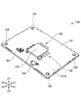
- FIG. 1 is a perspective view showing the appearance of the electronic device according to the embodiment.
- FIG. 2 is an exploded perspective view showing the configuration of the electronic device according to the embodiment.
- the electronic device 100 has a housing 170 including a case 110 and a cover 160. As shown in FIG. 2, the electronic device 100 further includes an antenna substrate 120, a radio wave absorber 130, a heat plate 140, and an elastic cushion 150 housed in a housing 170.
- FIG. 3A is a perspective view showing the configuration of the case 110.
- FIG. 3B is a perspective view showing the configuration of the antenna substrate 120.
- FIG. 3C is a perspective view showing the configuration of the radio wave absorber 130.
- FIG. 3D is a perspective view showing the configuration of the heat plate 140.
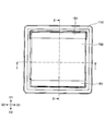
- FIG. 4A is a top view showing the electronic device 100 excluding the cover 160.
- FIG. 4B is a top view showing the electronic device 100 excluding the cover 160 and the elastic cushion 150.
- FIG. 4C is a top view showing the electronic device 100 excluding the cover 160, the elastic cushion 150, and the radio wave absorber 130.
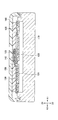
- 5A and 5B are cross-sectional views showing the configuration of the electronic device 100 according to the embodiment.
- FIG. 5A is a cross-sectional view taken along the line I-I in FIGS. 1, 4A, 4B, and 4C.
- FIG. 5B is a cross-sectional view taken along the line II-II in FIGS. 1, 4A, 4B, and 4C.
- the case 110 is made of, for example, aluminum or an aluminum alloy, and also serves as a heat sink.
- the planar shape of the case 110 is substantially square.
- the case 110 has four screw holes 112 into which screws 128 (see FIGS. 4B and 4C) for fixing the antenna board 120 to the case 110 are inserted, and screws 148 for fixing the heat plate 140 to the case 110 (FIG. 4B).
- FIG. 4C is formed with two screw holes 114 into which the holes are inserted.
- Guides 115 for guiding the side surfaces of the antenna substrate 120 are provided in the vicinity of the four screw holes 112 of the case 110, respectively.
- the case 110 is formed with a support portion 116 that supports the overhanging portion 132 of the radio wave absorber 130 described later.
- the antenna board 120 includes a wiring board 121, an antenna portion 122 formed on the wiring board 121, a semiconductor chip 123 mounted on the wiring board 121 and to which the antenna portion 122 is connected, and a wiring board. It has another semiconductor chip 124 mounted on 121.
- the antenna portion 122 is formed on the main surface 121A on the side opposite to the main surface facing the bottom of the wiring board 121, and the semiconductor chip 123 and the semiconductor chip 124 are arranged on the main surface 121A.
- the planar shape of the antenna substrate 120 is substantially rectangular, and through holes 129 through which screws 128 (see FIGS. 4B and 4C) pass through are formed at four corners thereof.
- the diameter of the through hole 129 is smaller than the diameter of the head of the screw 128. Therefore, the antenna board 120 can be fixed to the case 110 by using the screw 128.
- the antenna board 120 is arranged inside the guide 115.
- the semiconductor chip 123 includes an electronic circuit that transmits, receives, or transmits / receives radio waves through the antenna unit 122.
- the semiconductor chip 123 is, for example, a radar integrated circuit (IC) chip.
- the semiconductor chip 123 may include an electronic circuit that only transmits or receives radio waves through the antenna unit 122.
- the antenna substrate 120 is an example of a substrate
- the semiconductor chip 123 and the semiconductor chip 124 are examples of electronic components
- the main surface 121A is an example of one main surface.
- the radio wave absorber 130 has a base 131 having a substantially rectangular planar shape, and an overhang 132 that projects from the base 131 and is supported by the support 116.
- the base 131 includes a covering portion 133 that rises onto the semiconductor chip 123 mounted on the wiring board 121 and covers the semiconductor chip 123.
- the base 131 is formed with an opening 134 that exposes the antenna 122 in a plan view.
- Through holes 139 through which the screws 128 pass are formed at the four corners of the base 131.
- the diameter of the through hole 139 is larger than the diameter of the head of the screw 128. Therefore, in plan view, the screw 128 is located in the through hole 139.
- the radio wave absorber 130 is formed, for example, by mixing a soft magnetic powder with a base material of a silicone resin.
- the soft magnetic powder is, for example, a ferritic soft magnetic powder or a metal soft magnetic powder.
- As the material of the metallic soft magnetic powder for example, permalloy, sendust, silicon steel, permendur, pure iron, magnetic stainless steel and the like can be used.
- the radio wave absorber 130 has a sheet-like shape, and its thickness is, for example, 0.5 mm to 2.0 mm.
- the radio wave absorber 130 is arranged on the antenna substrate 120.
- the radio wave absorber 130 is an example of an electromagnetic wave absorber.
- the heat plate 140 has a fixing portion 141 fixed to the case 110 and an extending portion 142 extending from the fixing portion 141 to the upper side of the semiconductor chip 123.
- the planar shape of the fixing portion 141 is strip-shaped, and through holes 149 through which the screws 148 pass are formed at both ends thereof.
- the diameter of the through hole 149 is smaller than the diameter of the head of the screw 148. Therefore, the heat plate 140 can be fixed to the case 110 by using the screw 148.
- the fixing portion 141 is fixed to the case 110, the lower surface of the extending portion 142 comes into contact with the upper surface of the covering portion 133.
- the heat plate 140 is made of, for example, copper or a copper alloy.
- the heat generated by the semiconductor chip 123 is transferred to the extending portion 142 via the covering portion 133.
- the heat transferred to the extending portion 142 is transferred to the case 110 via the fixing portion 141, and is released from the case 110 to the outside.
- the heat plate 140 is an example of a heat transfer member.
- the elastic cushion 150 has a sheet-like shape having a substantially rectangular planar shape, and is elastically deformable in the thickness direction thereof.
- the thickness direction (Z1-Z2 direction) of the elastic cushion 150 is parallel to the normal direction (Z1-Z2 direction) of the main surface 121A of the wiring board 121.
- the material of the elastic cushion 150 is not particularly limited, and may include, for example, foamed plastic formed by foam-molding a synthetic resin.
- a soft foam of melamine resin can be used as the material of the elastic cushion 150.
- the relative permittivity of a soft foam of melamine resin is less than 2.0, the electrostatic tangent is 0.05, the tensile strength is 149 kPa, the elongation is 24%, the 40% compressive hardness is 11 kPa, and the 25% compressive hardness is 8. It is .5 kPa.
- a foamed material of a resin such as polyethylene, polystyrene, or polyurethane may be used, or a foamed material of styrene may be used.
- a material having a hollow structure and elastic in the thickness direction may be used for the elastic cushion 150.
- the elastic cushion 150 has a size such that the radio wave absorber 130 fits inside the elastic cushion 150 in a plan view.
- the thickness of the elastic cushion 150 is, for example, 2 mm to 10 mm.
- the double-sided adhesive tape 151 is attached to the upper surface of the elastic cushion 150, and the elastic cushion 150 is attached to the lower surface of the cover 160 via the double-sided adhesive tape 151.
- the elastic cushion 150 is an example of an elastic member.
- the cover 160 transmits radio waves transmitted, received or transmitted by the antenna unit 122.
- Examples of the material that transmits radio waves transmitted and received by the antenna unit 122 include a polyetherimide resin, a polybutylene terephthalate resin, and a polyphenylene sulfide resin.
- the cover 160 is fixed to the case 110.
- the distance between the lower surface of the cover 160 and the upper surface of the radio wave absorber 130 when the cover 160 is fixed to the case 110 is smaller than the thickness of the elastic cushion 150 when no stress is applied. Therefore, when the cover 160 is attached to the case 110, the cover 160 presses the elastic cushion 150 toward the antenna substrate 120 on the lower surface thereof, as shown in FIGS. 5A and 5B.
- the elastic cushion 150 is compressed between the lower surface of the cover 160 and the upper surface of the radio wave absorber 130.
- the elastic cushion 150 is compressed to a thickness of about 1 mm.
- the cover 160 is an example of a pressing member, and the lower surface of the cover 160 is an example of a pressing surface.
- the antenna substrate 120 is fixed to the case 110 using screws 128.
- the radio wave absorber 130 is arranged on the antenna substrate 120.
- the heat plate 140 is fixed to the case 110 by using screws 148 so that the lower surface of the extending portion 142 is in contact with the upper surface of the covering portion 133.
- the elastic cushion 150 is placed on the radio wave absorber 130 and the heat plate 140 so that the portion of the radio wave absorber 130 that overlaps the antenna substrate 120 in a plan view fits inside the elastic cushion 150. It is arranged. As shown in FIGS.
- the elastic cushion 150 is attached to the lower surface of the cover 160, and the lower surface of the cover 160 and the upper surface of the radio wave absorber 130 are connected to each other with the cover 160 attached to the case 110. It is compressed between.
- the elastic modulus of the radio wave absorber 130 is significantly higher than the elastic modulus of the elastic cushion 150. Therefore, although the radio wave absorber 130 applies compressive stress between the elastic cushion 150 and the antenna substrate 120, the amount of compressive deformation of the radio wave absorber 130 is significantly smaller than the amount of compressive deformation of the elastic cushion 150.
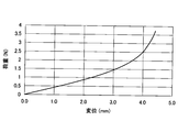
- FIG. 6A is a diagram showing an example of a load-displacement curve of the elastic cushion 150.
- FIG. 6B is a diagram showing an example of a load-displacement curve of the radio wave absorber 130.
- the radio wave absorber 130 can absorb unnecessary radio wave noise from the semiconductor chip 123, the semiconductor chip 124, and the antenna substrate 120, and transmit and receive desired radio waves through the antenna unit 122. it can.
- the repulsive force of the elastic cushion 150 compressed by the cover 160 fixed to the case 110 acts on the radio wave absorber 130, and the radio wave absorber 130 is pressed against the antenna substrate 120 to be in close contact with the radio wave absorber 130.
- the repulsive force of the elastic cushion 150 is stable even when it receives the heat of the semiconductor chip 123 and the semiconductor chip 124, and deterioration with the passage of time is unlikely to occur. Therefore, good adhesion between the radio wave absorber 130 and the antenna substrate 120 can be maintained for a long period of time, and the stability of the effect of absorbing radio wave noise by the radio wave absorber 130 can be improved.
- the repulsive force of the elastic cushion 150 compressed by the cover 160 fixed to the case 110 also acts on the extending portion 142, the extending portion 142 is pressed against the covering portion 133 and adheres to the covering portion 133, and the covering portion 133 is a semiconductor. It is pressed against the chip 123 and comes into close contact with it. Therefore, the heat generated by the semiconductor chip 123 is easily transferred to the extending portion 142 via the covering portion 133. As described above, the heat transferred to the extending portion 142 is transferred to the case 110 via the fixing portion 141 and released to the outside.
- the electromagnetic wave absorbed by the electromagnetic wave absorber is not limited to the radio wave transmitted and received via the antenna.
- an electromagnetic wave absorber that absorbs electromagnetic noise generated by a central processing unit (CPU) or the like provided on a substrate may be used.
Landscapes
- Engineering & Computer Science (AREA)
- Microelectronics & Electronic Packaging (AREA)
- Physics & Mathematics (AREA)
- Thermal Sciences (AREA)
- Shielding Devices Or Components To Electric Or Magnetic Fields (AREA)
- Cooling Or The Like Of Electrical Apparatus (AREA)
- Mounting Of Printed Circuit Boards And The Like (AREA)
Abstract
電子機器は、基板と、前記基板の一方の主面を覆う電磁波吸収体と、前記基板との間で前記電磁波吸収体を挟む位置に配置され、前記一方の主面の法線方向に弾性変形可能な弾性部材と、前記弾性部材を前記基板に向けて押圧する押圧部材と、を有する。
Description
本開示は、電子機器に関する。
特許文献1、2に、電磁波ノイズを吸収する電磁波吸収体を備えた電子機器が開示されている。
しかしながら、従来の電子機器が備えた電磁波吸収体は、電子機器内の電子部品の動作に伴う熱等の影響により、時間の経過とともに撓みや浮きを生じる等で位置が不安定になり、電磁波ノイズを十分に吸収できなくなることがある。
本開示は、電磁波ノイズの影響を安定して抑制することができる電子機器を提供することを目的とする。
本開示によれば、基板と、前記基板の一方の主面を覆う電磁波吸収体と、前記基板との間で前記電磁波吸収体を挟む位置に配置され、前記一方の主面の法線方向に弾性変形可能な弾性部材と、前記弾性部材を前記基板に向けて押圧する押圧部材と、を有する電子機器が提供される。
本開示によれば、電磁波ノイズの影響を安定して抑制することができる。
以下、本開示の実施形態について添付の図面を参照しながら具体的に説明する。なお、本明細書及び図面において、実質的に同一の機能構成を有する構成要素については、同一の符号を付することにより重複した説明を省くことがある。また、本開示においては、X1-X2方向、Y1-Y2方向、Z1-Z2方向を相互に直交する方向とする。また、X1-X2方向及びY1-Y2方向を含む面をXY面と記載し、Y1-Y2方向及びZ1-Z2方向を含む面をYZ面と記載し、Z1-Z2方向及びX1-X2方向を含む面をZX面と記載する。また、Z1-Z2方向を上下方向とし、平面視とは、Z1側から対象物をみることをいい、平面形状とは、Z1側からみた対象物の形状をいう。
図1は、実施形態に係る電子機器の外観を示す斜視図である。図2は、実施形態に係る電子機器の構成を示す分解斜視図である。
図1に示すように、実施形態に係る電子機器100は、ケース110とカバー160とを備えた筐体170を有する。図2に示すように、電子機器100は、更に、筐体170に収納された、アンテナ基板120と、電波吸収体130と、ヒートプレート140と、弾性クッション150とを有する。
図3Aは、ケース110の構成を示す斜視図である。図3Bは、アンテナ基板120の構成を示す斜視図である。図3Cは、電波吸収体130の構成を示す斜視図である。図3Dは、ヒートプレート140の構成を示す斜視図である。図4Aは、カバー160を除いた電子機器100を示す上面図である。図4Bは、カバー160及び弾性クッション150を除いた電子機器100を示す上面図である。図4Cは、カバー160、弾性クッション150及び電波吸収体130を除いた電子機器100を示す上面図である。図5A及び図5Bは、実施形態に係る電子機器100の構成を示す断面図である。図5Aは、図1、図4A、図4B、図4C中のI-I線に沿った断面図である。図5Bは、図1、図4A、図4B、図4C中のII-II線に沿った断面図である。
図3Aに示すように、ケース110は、例えばアルミニウム又はアルミニウム合金製であり、ヒートシンクを兼ねる。ケース110の平面形状は略正方形である。ケース110には、アンテナ基板120をケース110に固定するねじ128(図4B、図4C参照)が挿入される4個のねじ穴112と、ヒートプレート140をケース110に固定するねじ148(図4B、図4C参照)が挿入される2個のねじ穴114とが形成されている。ケース110の4個のねじ穴112の近傍には、それぞれアンテナ基板120の側面を案内するガイド115が設けられている。また、ケース110には、後述の電波吸収体130の張り出し部132を支持する支持部116が形成されている。
図3Bに示すように、アンテナ基板120は、配線基板121と、配線基板121に形成されたアンテナ部122と、配線基板121に実装され、アンテナ部122が接続された半導体チップ123と、配線基板121に実装されたその他の半導体チップ124とを有する。例えば、アンテナ部122は、配線基板121の底と対向する主面とは反対側の主面121Aに形成されており、半導体チップ123及び半導体チップ124は、主面121A上に配置されている。アンテナ基板120の平面形状は略長方形であり、その4隅にねじ128(図4B、図4C参照)が貫通する貫通孔129が形成されている。貫通孔129の直径は、ねじ128の頭部の直径よりも小さい。従って、ねじ128を用いて、アンテナ基板120をケース110に固定することができる。アンテナ基板120は、ガイド115の内側に配置される。半導体チップ123は、アンテナ部122を通じて電波の送信、受信又は送受信を行う電子回路を含む。半導体チップ123は、例えばレーダ集積回路(integrated circuit:IC)チップである。半導体チップ123が、アンテナ部122を通じて電波の送信のみ又は受信のみを行う電子回路を含んでいてもよい。アンテナ基板120は基板の一例であり、半導体チップ123及び半導体チップ124は電子部品の一例であり、主面121Aは一方の主面の一例である。
図3C及び図4Bに示すように、電波吸収体130は、平面形状が略長方形の基部131と、基部131から張り出し、支持部116に支持される張り出し部132とを有する。基部131は、配線基板121に実装された半導体チップ123上にせり上がり、半導体チップ123を覆う被覆部133を含む。基部131には、平面視でアンテナ部122を露出する開口部134が形成されている。基部131の4隅にねじ128が貫通する貫通孔139が形成されている。貫通孔139の直径は、ねじ128の頭部の直径よりも大きい。従って、平面視でねじ128は貫通孔139内に位置する。電波吸収体130は、例えば、シリコーン系樹脂の基材に軟磁性粉体を混合して形成されている。軟磁性粉体は、例えば、フェライト系軟磁性粉体又は金属系軟磁性粉体である。金属系軟磁性粉体の材料としては、例えばパーマロイ、センダスト、ケイ素鋼、パーメンジュール、純鉄、磁性ステンレス鋼等を用いることができる。例えば、電波吸収体130はシート状の形状を有しており、その厚さは例えば0.5mm~2.0mmである。電波吸収体130は、アンテナ基板120上に配置される。電波吸収体130は電磁波吸収体の一例である。
図3D、図4B及び図4Cに示すように、ヒートプレート140は、ケース110に固定される固定部141と、固定部141から半導体チップ123の上方まで延出する延出部142とを有する。固定部141の平面形状は帯状であり、その両端にねじ148が貫通する貫通孔149が形成されている。貫通孔149の直径は、ねじ148の頭部の直径よりも小さい。従って、ねじ148を用いて、ヒートプレート140をケース110に固定することができる。固定部141がケース110に固定されたとき、延出部142の下面は被覆部133の上面に接触する。ヒートプレート140は、例えば銅又は銅合金製である。半導体チップ123が発した熱は、被覆部133を介して延出部142に伝達される。延出部142に伝達された熱は、固定部141を介してケース110に伝達され、ケース110から外部に放出される。ヒートプレート140は伝熱部材の一例である。
図2及び図4Aに示すように、弾性クッション150は、平面形状が略長方形のシート状の形状を有し、その厚さ方向に弾性変形可能である。弾性クッション150の厚さ方向(Z1-Z2方向)は、配線基板121の主面121Aの法線方向(Z1-Z2方向)と平行である。弾性クッション150の材料は特に限定されず、例えば、合成樹脂が発泡成形されて構成された発泡プラスチックを含むことができる。例えば、弾性クッション150の材料にメラミン樹脂の軟質フォームを用いることができる。例えば、メラミン樹脂の軟質フォームの比誘電率は2.0未満、静電正接は0.05、引張強度は149kPa、伸びは24%、40%圧縮硬さは11kPa、25%圧縮硬さは8.5kPaである。弾性クッション150の材料に、ポリエチレン、ポリスチレン、ポリウレタン等の樹脂の発泡材料を用いてもよく、スチロールの発泡材料を用いてもよい。また、中空構造を備え、厚さ方向に弾性可能な材料を弾性クッション150に用いてもよい。弾性クッション150は、平面視で、電波吸収体130が弾性クッション150の内側に収まる程度の大きさを有する。弾性クッション150の厚さは、例えば2mm~10mmである。弾性クッション150の上面に両面接着テープ151が貼り付けられており、弾性クッション150は両面接着テープ151を介してカバー160の下面に貼り付けられている。弾性クッション150は弾性部材の一例である。
カバー160は、アンテナ部122が送信、受信又は送受信する電波を透過させる。アンテナ部122が送受信する電波を透過させる材料として、ポリエーテルイミド樹脂、ポリブチレンテレフタレート樹脂及びポリフェニレンサルファイド樹脂が挙げられる。カバー160はケース110に固定される。カバー160がケース110に固定されたときのカバー160の下面と電波吸収体130の上面との間の距離は、応力が印加されていないときの弾性クッション150の厚さよりも小さい。従って、カバー160がケース110に取り付けられると、図5A及び図5Bに示すように、カバー160はその下面で弾性クッション150をアンテナ基板120に向けて押圧する。この結果、カバー160の下面と電波吸収体130の上面との間で、弾性クッション150が圧縮される。例えば、最も薄いところ(ヒートプレート140の延出部142の先端に接する部分)で、弾性クッション150は1mm程度の厚さまで圧縮される。カバー160は押圧部材の一例であり、カバー160の下面は押圧面の一例である。
図4B及び図4Cに示すように、ねじ128を用いてアンテナ基板120がケース110に固定されている。図4Bに示すように、アンテナ基板120の上に電波吸収体130が配置されている。図4B、図4C及び図5Bに示すように、延出部142の下面が被覆部133の上面に接するようにして、ねじ148を用いてヒートプレート140がケース110に固定されている。図4Aに示すように、弾性クッション150が、電波吸収体130及びヒートプレート140の上に、平面視で、電波吸収体130のアンテナ基板120と重なる部分が弾性クッション150の内側に収まるようにして配置されている。図5A及び図5Bに示すように、弾性クッション150はカバー160の下面に貼り付けられており、カバー160がケース110に取り付けられた状態で、カバー160の下面と電波吸収体130の上面との間で圧縮されている。電波吸収体130の弾性率は弾性クッション150の弾性率よりも著しく高い。従って、電波吸収体130は、弾性クッション150とアンテナ基板120との間で圧縮応力を印加されるものの、電波吸収体130の圧縮変形量は、弾性クッション150の圧縮変形量よりも著しく小さい。図6Aは、弾性クッション150の荷重-変位曲線の一例を示す図である。図6Bは、電波吸収体130の荷重-変位曲線の一例を示す図である。
このように構成された電子機器100では、電波吸収体130が半導体チップ123、半導体チップ124やアンテナ基板120からの不要な電波ノイズを吸収し、アンテナ部122を通じて所望の電波の送受信を行うことができる。
また、ケース110に固定されたカバー160により圧縮された弾性クッション150の反発力が電波吸収体130に作用し、電波吸収体130がアンテナ基板120に押し付けられて密着する。弾性クッション150の反発力は、半導体チップ123及び半導体チップ124の熱を受けても安定しており、また、時間の経過に伴う劣化が生じにくい。従って、長期にわたって、電波吸収体130とアンテナ基板120との間の密着性を良好に維持することができ、電波吸収体130による電波ノイズを吸収する効果の安定性を向上することができる。
また、ケース110に固定されたカバー160により圧縮された弾性クッション150の反発力は延出部142にも作用し、延出部142が被覆部133に押し付けられて密着し、被覆部133が半導体チップ123に押し付けられて密着する。従って、半導体チップ123が発した熱が被覆部133を介して延出部142に伝達されやすい。上記のように、延出部142に伝達された熱は固定部141を介してケース110に伝達され、外部に放出される。
なお、本開示において、電磁波吸収体が吸収する電磁波はアンテナを介して送受信される電波に限定されない。例えば、基板に設けられた中央処理装置(central processing unit:CPU)等が発する電磁雑音を吸収する電磁波吸収体が用いられてもよい。
以上、好ましい実施の形態等について詳説したが、上述した実施の形態等に制限されることはなく、請求の範囲に記載された範囲を逸脱することなく、上述した実施の形態等に種々の変形及び置換を加えることができる。
本国際出願は、2019年3月18日に出願した日本国特許出願第2019-050297号に基づく優先権を主張するものであり、当該出願の全内容を本国際出願に援用する。
100 電子機器
110 ケース
120 アンテナ基板
121 配線基板
122 アンテナ部
123、124 半導体チップ
130 電波吸収体
133 被覆部
134 開口部
140 ヒートプレート
141 固定部
142 延出部
150 弾性クッション
160 カバー
170 筐体
110 ケース
120 アンテナ基板
121 配線基板
122 アンテナ部
123、124 半導体チップ
130 電波吸収体
133 被覆部
134 開口部
140 ヒートプレート
141 固定部
142 延出部
150 弾性クッション
160 カバー
170 筐体
Claims (10)
- 基板と、
前記基板の一方の主面を覆う電磁波吸収体と、
前記基板との間で前記電磁波吸収体を挟む位置に配置され、前記一方の主面の法線方向に弾性変形可能な弾性部材と、
前記弾性部材を前記基板に向けて押圧する押圧部材と、
を有することを特徴とする電子機器。 - 前記電磁波吸収体及び前記弾性部材は、シート状の形状を有することを特徴とする請求項1に記載の電子機器。
- 前記弾性部材は、合成樹脂が発泡成形されて構成された発泡プラスチックを含むことを特徴とする請求項1又は2に記載の電子機器。
- 前記押圧部材は、前記弾性部材を押圧する押圧面を有することを特徴とする請求項1乃至3のいずれか1項に記載の電子機器。
- 前記一方の主面の法線方向からみたときに、前記電磁波吸収体の前記基板と重なる部分が前記弾性部材の内側に収まることを特徴とする請求項1乃至4のいずれか1項に記載の電子機器。
- 前記基板は、アンテナを有し、
前記一方の主面の法線方向からみたときに、前記電磁波吸収体に、前記アンテナを露出する開口部が形成されていることを特徴とする請求項1乃至5のいずれか1項に記載の電子機器。 - 前記押圧部材は、前記アンテナが送信、受信又は送受信する電波を透過させることを特徴とする請求項6に記載の電子機器。
- 前記基板は、前記一方の主面に実装された電子部品を有することを特徴とする請求項1乃至7のいずれか1項に記載の電子機器。
- 前記電子部品と前記弾性部材との間に、前記電子部品が発した熱を伝達する伝熱部材を有することを特徴とする請求項8に記載の電子機器。
- 前記電子部品は、電波の送信、受信又は送受信を行う電子回路を含むことを特徴とする請求項8又は9に記載の電子機器。
Applications Claiming Priority (2)
| Application Number | Priority Date | Filing Date | Title |
|---|---|---|---|
| JP2019050297A JP2022070283A (ja) | 2019-03-18 | 2019-03-18 | 電子機器 |
| JP2019-050297 | 2019-03-18 |
Publications (1)
| Publication Number | Publication Date |
|---|---|
| WO2020189136A1 true WO2020189136A1 (ja) | 2020-09-24 |
Family
ID=72520155
Family Applications (1)
| Application Number | Title | Priority Date | Filing Date |
|---|---|---|---|
| PCT/JP2020/006123 Ceased WO2020189136A1 (ja) | 2019-03-18 | 2020-02-17 | 電子機器 |
Country Status (2)
| Country | Link |
|---|---|
| JP (1) | JP2022070283A (ja) |
| WO (1) | WO2020189136A1 (ja) |
Citations (4)
| Publication number | Priority date | Publication date | Assignee | Title |
|---|---|---|---|---|
| JPH04140905A (ja) * | 1990-10-01 | 1992-05-14 | Hitachi Chem Co Ltd | 平面アンテナ |
| JP2013115615A (ja) * | 2011-11-29 | 2013-06-10 | Nec Casio Mobile Communications Ltd | 電子機器 |
| JP2014179515A (ja) * | 2013-03-15 | 2014-09-25 | Mitsubishi Electric Corp | 電子機器 |
| JP2018171916A (ja) * | 2017-03-30 | 2018-11-08 | 積水化学工業株式会社 | 発泡複合体 |
-
2019
- 2019-03-18 JP JP2019050297A patent/JP2022070283A/ja active Pending
-
2020
- 2020-02-17 WO PCT/JP2020/006123 patent/WO2020189136A1/ja not_active Ceased
Patent Citations (4)
| Publication number | Priority date | Publication date | Assignee | Title |
|---|---|---|---|---|
| JPH04140905A (ja) * | 1990-10-01 | 1992-05-14 | Hitachi Chem Co Ltd | 平面アンテナ |
| JP2013115615A (ja) * | 2011-11-29 | 2013-06-10 | Nec Casio Mobile Communications Ltd | 電子機器 |
| JP2014179515A (ja) * | 2013-03-15 | 2014-09-25 | Mitsubishi Electric Corp | 電子機器 |
| JP2018171916A (ja) * | 2017-03-30 | 2018-11-08 | 積水化学工業株式会社 | 発泡複合体 |
Also Published As
| Publication number | Publication date |
|---|---|
| JP2022070283A (ja) | 2022-05-13 |
Similar Documents
| Publication | Publication Date | Title |
|---|---|---|
| CN110087172B (zh) | 一种屏幕发声设备 | |
| US10866655B2 (en) | Touchpad module | |
| JP5992111B1 (ja) | ユニット取付装置、電子機器システムおよびユニット取付装置の製造方法 | |
| KR102264330B1 (ko) | 터치센서 모듈 | |
| JP6000170B2 (ja) | 電子機器 | |
| JP7342732B2 (ja) | 電子装置 | |
| JPWO2017022221A1 (ja) | 放熱構造および電子機器 | |
| US20130335644A1 (en) | Television and electronic apparatus | |
| JP2009016398A (ja) | プリント配線板構造、電子部品の実装方法および電子機器 | |
| US20160135282A1 (en) | Electronic apparatus | |
| US10429966B2 (en) | Touch input device | |
| JP2022070283A (ja) | 電子機器 | |
| US10177441B2 (en) | Antenna module | |
| CN213423800U (zh) | 电子设备 | |
| TW201813478A (zh) | 背板 | |
| JP4798629B2 (ja) | 熱伝導性電磁波シールドシート及び電磁波シールド構造 | |
| WO2016051720A1 (ja) | シールドカバーおよび電子機器 | |
| JP4475162B2 (ja) | 携帯型電子機器 | |
| JP5032167B2 (ja) | 電子機器 | |
| WO2007061245A1 (en) | Ic holder | |
| JP2015159251A (ja) | 実装基板及び電子機器 | |
| JP2019083262A (ja) | プリント回路板 | |
| JP5050093B2 (ja) | 電子機器 | |
| JP2002185183A (ja) | 電磁波抑制シート及び電磁波抑制熱伝導シート | |
| TW201440603A (zh) | 電子裝置 |
Legal Events
| Date | Code | Title | Description |
|---|---|---|---|
| 121 | Ep: the epo has been informed by wipo that ep was designated in this application |
Ref document number: 20773207 Country of ref document: EP Kind code of ref document: A1 |
|
| NENP | Non-entry into the national phase |
Ref country code: DE |
|
| 122 | Ep: pct application non-entry in european phase |
Ref document number: 20773207 Country of ref document: EP Kind code of ref document: A1 |
|
| NENP | Non-entry into the national phase |
Ref country code: JP |