WO2020189041A1 - Fc型3レベル電力変換装置 - Google Patents
Fc型3レベル電力変換装置 Download PDFInfo
- Publication number
- WO2020189041A1 WO2020189041A1 PCT/JP2020/003319 JP2020003319W WO2020189041A1 WO 2020189041 A1 WO2020189041 A1 WO 2020189041A1 JP 2020003319 W JP2020003319 W JP 2020003319W WO 2020189041 A1 WO2020189041 A1 WO 2020189041A1
- Authority
- WO
- WIPO (PCT)
- Prior art keywords
- semiconductor switching
- voltage
- filter capacitor
- switching elements
- turned
- Prior art date
- Legal status (The legal status is an assumption and is not a legal conclusion. Google has not performed a legal analysis and makes no representation as to the accuracy of the status listed.)
- Ceased
Links
Images






Classifications
-
- H—ELECTRICITY
- H02—GENERATION; CONVERSION OR DISTRIBUTION OF ELECTRIC POWER
- H02M—APPARATUS FOR CONVERSION BETWEEN AC AND AC, BETWEEN AC AND DC, OR BETWEEN DC AND DC, AND FOR USE WITH MAINS OR SIMILAR POWER SUPPLY SYSTEMS; CONVERSION OF DC OR AC INPUT POWER INTO SURGE OUTPUT POWER; CONTROL OR REGULATION THEREOF
- H02M7/00—Conversion of AC power input into DC power output; Conversion of DC power input into AC power output
- H02M7/42—Conversion of DC power input into AC power output without possibility of reversal
- H02M7/44—Conversion of DC power input into AC power output without possibility of reversal by static converters
- H02M7/48—Conversion of DC power input into AC power output without possibility of reversal by static converters using discharge tubes with control electrode or semiconductor devices with control electrode
- H02M7/483—Converters with outputs that each can have more than two voltages levels
- H02M7/4833—Capacitor voltage balancing
-
- H—ELECTRICITY
- H02—GENERATION; CONVERSION OR DISTRIBUTION OF ELECTRIC POWER
- H02M—APPARATUS FOR CONVERSION BETWEEN AC AND AC, BETWEEN AC AND DC, OR BETWEEN DC AND DC, AND FOR USE WITH MAINS OR SIMILAR POWER SUPPLY SYSTEMS; CONVERSION OF DC OR AC INPUT POWER INTO SURGE OUTPUT POWER; CONTROL OR REGULATION THEREOF
- H02M1/00—Details of apparatus for conversion
- H02M1/44—Circuits or arrangements for compensating for electromagnetic interference in converters or inverters
-
- H—ELECTRICITY
- H02—GENERATION; CONVERSION OR DISTRIBUTION OF ELECTRIC POWER
- H02M—APPARATUS FOR CONVERSION BETWEEN AC AND AC, BETWEEN AC AND DC, OR BETWEEN DC AND DC, AND FOR USE WITH MAINS OR SIMILAR POWER SUPPLY SYSTEMS; CONVERSION OF DC OR AC INPUT POWER INTO SURGE OUTPUT POWER; CONTROL OR REGULATION THEREOF
- H02M3/00—Conversion of DC power input into DC power output
- H02M3/02—Conversion of DC power input into DC power output without intermediate conversion into AC
- H02M3/04—Conversion of DC power input into DC power output without intermediate conversion into AC by static converters
- H02M3/10—Conversion of DC power input into DC power output without intermediate conversion into AC by static converters using discharge tubes with control electrode or semiconductor devices with control electrode
- H02M3/145—Conversion of DC power input into DC power output without intermediate conversion into AC by static converters using discharge tubes with control electrode or semiconductor devices with control electrode using devices of a triode or transistor type requiring continuous application of a control signal
- H02M3/155—Conversion of DC power input into DC power output without intermediate conversion into AC by static converters using discharge tubes with control electrode or semiconductor devices with control electrode using devices of a triode or transistor type requiring continuous application of a control signal using semiconductor devices only
- H02M3/156—Conversion of DC power input into DC power output without intermediate conversion into AC by static converters using discharge tubes with control electrode or semiconductor devices with control electrode using devices of a triode or transistor type requiring continuous application of a control signal using semiconductor devices only with automatic control of output voltage or current, e.g. switching regulators
- H02M3/158—Conversion of DC power input into DC power output without intermediate conversion into AC by static converters using discharge tubes with control electrode or semiconductor devices with control electrode using devices of a triode or transistor type requiring continuous application of a control signal using semiconductor devices only with automatic control of output voltage or current, e.g. switching regulators including plural semiconductor devices as final control devices for a single load
-
- H—ELECTRICITY
- H02—GENERATION; CONVERSION OR DISTRIBUTION OF ELECTRIC POWER
- H02M—APPARATUS FOR CONVERSION BETWEEN AC AND AC, BETWEEN AC AND DC, OR BETWEEN DC AND DC, AND FOR USE WITH MAINS OR SIMILAR POWER SUPPLY SYSTEMS; CONVERSION OF DC OR AC INPUT POWER INTO SURGE OUTPUT POWER; CONTROL OR REGULATION THEREOF
- H02M7/00—Conversion of AC power input into DC power output; Conversion of DC power input into AC power output
- H02M7/42—Conversion of DC power input into AC power output without possibility of reversal
- H02M7/44—Conversion of DC power input into AC power output without possibility of reversal by static converters
- H02M7/48—Conversion of DC power input into AC power output without possibility of reversal by static converters using discharge tubes with control electrode or semiconductor devices with control electrode
- H02M7/483—Converters with outputs that each can have more than two voltages levels
-
- H—ELECTRICITY
- H02—GENERATION; CONVERSION OR DISTRIBUTION OF ELECTRIC POWER
- H02M—APPARATUS FOR CONVERSION BETWEEN AC AND AC, BETWEEN AC AND DC, OR BETWEEN DC AND DC, AND FOR USE WITH MAINS OR SIMILAR POWER SUPPLY SYSTEMS; CONVERSION OF DC OR AC INPUT POWER INTO SURGE OUTPUT POWER; CONTROL OR REGULATION THEREOF
- H02M7/00—Conversion of AC power input into DC power output; Conversion of DC power input into AC power output
- H02M7/42—Conversion of DC power input into AC power output without possibility of reversal
- H02M7/44—Conversion of DC power input into AC power output without possibility of reversal by static converters
- H02M7/48—Conversion of DC power input into AC power output without possibility of reversal by static converters using discharge tubes with control electrode or semiconductor devices with control electrode
- H02M7/53—Conversion of DC power input into AC power output without possibility of reversal by static converters using discharge tubes with control electrode or semiconductor devices with control electrode using devices of a triode or transistor type requiring continuous application of a control signal
- H02M7/537—Conversion of DC power input into AC power output without possibility of reversal by static converters using discharge tubes with control electrode or semiconductor devices with control electrode using devices of a triode or transistor type requiring continuous application of a control signal using semiconductor devices only, e.g. single switched pulse inverters
- H02M7/5387—Conversion of DC power input into AC power output without possibility of reversal by static converters using discharge tubes with control electrode or semiconductor devices with control electrode using devices of a triode or transistor type requiring continuous application of a control signal using semiconductor devices only, e.g. single switched pulse inverters in a bridge configuration
-
- H—ELECTRICITY
- H02—GENERATION; CONVERSION OR DISTRIBUTION OF ELECTRIC POWER
- H02M—APPARATUS FOR CONVERSION BETWEEN AC AND AC, BETWEEN AC AND DC, OR BETWEEN DC AND DC, AND FOR USE WITH MAINS OR SIMILAR POWER SUPPLY SYSTEMS; CONVERSION OF DC OR AC INPUT POWER INTO SURGE OUTPUT POWER; CONTROL OR REGULATION THEREOF
- H02M1/00—Details of apparatus for conversion
- H02M1/0067—Converter structures employing plural converter units, other than for parallel operation of the units on a single load
- H02M1/0074—Plural converter units whose inputs are connected in series
-
- H—ELECTRICITY
- H02—GENERATION; CONVERSION OR DISTRIBUTION OF ELECTRIC POWER
- H02M—APPARATUS FOR CONVERSION BETWEEN AC AND AC, BETWEEN AC AND DC, OR BETWEEN DC AND DC, AND FOR USE WITH MAINS OR SIMILAR POWER SUPPLY SYSTEMS; CONVERSION OF DC OR AC INPUT POWER INTO SURGE OUTPUT POWER; CONTROL OR REGULATION THEREOF
- H02M1/00—Details of apparatus for conversion
- H02M1/0067—Converter structures employing plural converter units, other than for parallel operation of the units on a single load
- H02M1/0077—Plural converter units whose outputs are connected in series
-
- H—ELECTRICITY
- H02—GENERATION; CONVERSION OR DISTRIBUTION OF ELECTRIC POWER
- H02M—APPARATUS FOR CONVERSION BETWEEN AC AND AC, BETWEEN AC AND DC, OR BETWEEN DC AND DC, AND FOR USE WITH MAINS OR SIMILAR POWER SUPPLY SYSTEMS; CONVERSION OF DC OR AC INPUT POWER INTO SURGE OUTPUT POWER; CONTROL OR REGULATION THEREOF
- H02M1/00—Details of apparatus for conversion
- H02M1/0095—Hybrid converter topologies, e.g. NPC mixed with flying capacitor, thyristor converter mixed with MMC or charge pump mixed with buck
-
- H—ELECTRICITY
- H02—GENERATION; CONVERSION OR DISTRIBUTION OF ELECTRIC POWER
- H02M—APPARATUS FOR CONVERSION BETWEEN AC AND AC, BETWEEN AC AND DC, OR BETWEEN DC AND DC, AND FOR USE WITH MAINS OR SIMILAR POWER SUPPLY SYSTEMS; CONVERSION OF DC OR AC INPUT POWER INTO SURGE OUTPUT POWER; CONTROL OR REGULATION THEREOF
- H02M7/00—Conversion of AC power input into DC power output; Conversion of DC power input into AC power output
- H02M7/42—Conversion of DC power input into AC power output without possibility of reversal
- H02M7/44—Conversion of DC power input into AC power output without possibility of reversal by static converters
- H02M7/48—Conversion of DC power input into AC power output without possibility of reversal by static converters using discharge tubes with control electrode or semiconductor devices with control electrode
- H02M7/483—Converters with outputs that each can have more than two voltages levels
- H02M7/4837—Flying capacitor converters
-
- H—ELECTRICITY
- H02—GENERATION; CONVERSION OR DISTRIBUTION OF ELECTRIC POWER
- H02M—APPARATUS FOR CONVERSION BETWEEN AC AND AC, BETWEEN AC AND DC, OR BETWEEN DC AND DC, AND FOR USE WITH MAINS OR SIMILAR POWER SUPPLY SYSTEMS; CONVERSION OF DC OR AC INPUT POWER INTO SURGE OUTPUT POWER; CONTROL OR REGULATION THEREOF
- H02M7/00—Conversion of AC power input into DC power output; Conversion of DC power input into AC power output
- H02M7/42—Conversion of DC power input into AC power output without possibility of reversal
- H02M7/44—Conversion of DC power input into AC power output without possibility of reversal by static converters
- H02M7/48—Conversion of DC power input into AC power output without possibility of reversal by static converters using discharge tubes with control electrode or semiconductor devices with control electrode
- H02M7/53—Conversion of DC power input into AC power output without possibility of reversal by static converters using discharge tubes with control electrode or semiconductor devices with control electrode using devices of a triode or transistor type requiring continuous application of a control signal
- H02M7/537—Conversion of DC power input into AC power output without possibility of reversal by static converters using discharge tubes with control electrode or semiconductor devices with control electrode using devices of a triode or transistor type requiring continuous application of a control signal using semiconductor devices only, e.g. single switched pulse inverters
- H02M7/539—Conversion of DC power input into AC power output without possibility of reversal by static converters using discharge tubes with control electrode or semiconductor devices with control electrode using devices of a triode or transistor type requiring continuous application of a control signal using semiconductor devices only, e.g. single switched pulse inverters with automatic control of output wave form or frequency
-
- Y—GENERAL TAGGING OF NEW TECHNOLOGICAL DEVELOPMENTS; GENERAL TAGGING OF CROSS-SECTIONAL TECHNOLOGIES SPANNING OVER SEVERAL SECTIONS OF THE IPC; TECHNICAL SUBJECTS COVERED BY FORMER USPC CROSS-REFERENCE ART COLLECTIONS [XRACs] AND DIGESTS
- Y02—TECHNOLOGIES OR APPLICATIONS FOR MITIGATION OR ADAPTATION AGAINST CLIMATE CHANGE
- Y02B—CLIMATE CHANGE MITIGATION TECHNOLOGIES RELATED TO BUILDINGS, e.g. HOUSING, HOUSE APPLIANCES OR RELATED END-USER APPLICATIONS
- Y02B70/00—Technologies for an efficient end-user side electric power management and consumption
- Y02B70/10—Technologies improving the efficiency by using switched-mode power supplies [SMPS], i.e. efficient power electronics conversion e.g. power factor correction or reduction of losses in power supplies or efficient standby modes
Definitions
- the present invention relates to voltage control of a flying capacitor and a filter capacitor in a flying capacitor (FC) type three-level power converter.
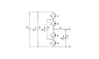
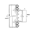
- FIG. 21 shows the FC type 3-level chopper circuit described in Patent Document 1
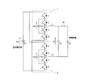
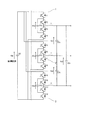
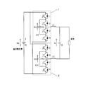
- FIG. 22 shows a configuration example of an FC-type 3-level converter having a plurality of units and capable of differential output.
- the FC type 3 level chopper circuit as shown in FIG. 21 and the FC type 3 level converter as shown in FIG. 22 are included in the term FC type 3 level power converter.
- the FC type 3-level power converter has half the output voltage ripple compared to the 2-level. Further, since the breaking voltage is also halved, the switching loss of the semiconductor switching element is reduced, and the switching frequency can be easily increased. This feature is suitable for equipment that requires high efficiency, high response speed, and low ripple.
- Patent Documents 2 and 3 disclose an FC voltage control method for an FC type 3-level inverter, which can be directly applied to an FC-type 3-level chopper circuit.
- the first to eighth semiconductor switching elements T1 to T8 are turned on or off to perform the first and first operations. While controlling the second flying capacitor voltages Vfc1 and Vfc2 to E / 2 (half of Vdc), the three-level voltage (E, E / 2,0) is the connection point of the second and third semiconductor switching elements T2 and T3. , 6th and 7th semiconductor switching elements T6, T7 are output from the connection points and applied to the load.
- FC type 3-level converter Details of the FC type 3-level converter are disclosed in General Documents and Patent Document 5.
- the device In order to control the flying capacitor voltage using Patent Documents 2 and 3, the device needs to output a current. Therefore, while the device is stopped, the flying capacitor voltage decreases due to natural discharge. In addition, a separate means for charging the flying capacitor voltage to about half of the DC voltage is required before operation.
- a filter capacitor is connected to a general power conversion device for the purpose of removing switching ripples.
- a battery is connected to a device, an inrush current flows from the battery to the filter capacitor. To prevent this, it is necessary to charge the filter capacitor to the same voltage as the battery in advance. Since Patent Document 4 does not assume the connection of the filter capacitor, the filter capacitor cannot be charged.
- the present invention has been devised in view of the above-mentioned conventional problems, and one aspect thereof is a first in which a filter capacitor on the high pressure side and the positive and negative sides of the filter capacitor on the high pressure side are sequentially connected in series.
- the flying capacitors connected between the first to fourth semiconductor switching elements, the connection points of the first and second semiconductor switching elements, and the connection points of the third and fourth semiconductor switching elements, and the second and second semiconductor switching elements.
- a filter reactor having one end connected to a connection point of a semiconductor switching element, a low-voltage side filter capacitor connected between the other end of the filter reactor and the negative electrode of the high-voltage side filter capacitor, and the high-voltage side
- An FC type 3-level power converter including a filter capacitor or a DC voltage source connected in parallel to the low-voltage side filter capacitor, which is 1 / of the flying capacitor voltage and the high-voltage side filter capacitor voltage. Comparison with 2, and comparison between the high pressure side filter capacitor voltage and the flying capacitor voltage + low pressure side filter capacitor voltage, comparison between the flying capacitor voltage and the low pressure side filter capacitor voltage, and the low pressure side.
- the first to fourth semiconductor switching elements are turned ON or OFF, and a current is applied to the path including the filter reactor.
- the flying capacitor and the low-voltage side filter capacitor or the high-voltage side filter capacitor are charged to a predetermined value.
- the filter capacitor on the high pressure side, the fourth to first semiconductor switching elements sequentially connected in series between the positive and negative sides of the filter capacitor on the high pressure side, and the fourth and third semiconductors.
- a flying capacitor connected between the connection point of the switching element and the connection point of the second and first semiconductor switching elements, and a filter reactor having one end connected to the connection point of the third and second semiconductor switching elements.
- the low-voltage side filter capacitor connected between the other end of the filter reactor and the positive electrode of the high-voltage side filter capacitor, and the high-voltage side filter capacitor or the low-voltage side filter capacitor connected in parallel.
- An FC type 3-level power converter equipped with a DC voltage source, which compares the flying capacitor voltage with 1/2 of the high-pressure side filter capacitor voltage, and the high-pressure side filter capacitor voltage and the above. Comparison of flying capacitor voltage + low-voltage side filter capacitor voltage, comparison of the flying capacitor voltage with the low-voltage side filter capacitor voltage, and the low-voltage side filter capacitor voltage or the high-voltage side filter capacitor voltage and filter capacitor. Based on the comparison with the voltage command value, the first to fourth semiconductor switching elements are turned ON or OFF to pass a current through the path including the filter reactor, and the flying capacitor and the low-voltage side filter capacitor or the high-voltage capacitor are applied. It is characterized in that the filter capacitor on the side is charged to a predetermined value.
- the first to fourth semiconductor switching elements sequentially connected in series between the positive and negative sides of the DC voltage source, the connection points of the first and second semiconductor switching elements, and the third and third semiconductor switching elements.
- a first unit having a first flying capacitor connected to a connection point of a fourth semiconductor switching element, and fifth to eighth units sequentially connected in series between the positive and negative sides of the DC voltage source.
- a second unit having a semiconductor switching element and a second flying capacitor connected between the connection points of the fifth and sixth semiconductor switching elements and the connection points of the seventh and eighth semiconductor switching elements.
- the first filter reactor having one end connected to the connection point of the second and third semiconductor switching elements, the second filter reactor having one end connected to the connection point of the sixth and seventh semiconductor switching elements, and the second filter reactor.
- An FC type 3-level power converter equipped with a filter capacitor connected between the other ends of the 1st and 2nd filter reactors, which is 1/2 of the 1st and 2nd flying capacitor voltage and the DC voltage source voltage. Comparison with, and comparison between the filter capacitor voltage and the filter capacitor voltage command value, and comparison between the DC voltage source voltage and the first flying capacitor voltage + the second flying capacitor voltage + the filter capacitor voltage command value. , And the comparison between the DC voltage source voltage and the first flying capacitor voltage + the second flying capacitor voltage-the filter capacitor voltage command value, and the first and second flying capacitor voltages and the filter capacitor voltage.
- the first to eighth semiconductor switching elements are turned ON or OFF based on the comparison of the first flying capacitor voltage and the second flying capacitor voltage, and the first and second filter reactors are included. A current is passed through the path to charge the first and second flying capacitors and the filter capacitor to predetermined values.
- the first in the case where the DC voltage source is connected in parallel to the filter capacitor on the high voltage side and Vfc ⁇ Va / 2 and Vb ⁇ Vb * and Va> Vfc + Vb + ⁇ , the first.
- the semiconductor switching element When the semiconductor switching element is turned on, the second, third, and fourth semiconductor switching elements are turned off, and Vfc ⁇ Va / 2, Vb ⁇ Vb *, and Va ⁇ Vfc + Vb + ⁇ , the first and second semiconductor switching elements are turned on.
- the second semiconductor switching element When the first, second, and third semiconductor switching elements are turned off and Vfc ⁇ Va / 2, Vb ⁇ Vb *, and Vfc> Vb + ⁇ , the second semiconductor switching element is turned on, and the first and first semiconductor switching elements are turned on.
- the third and fourth semiconductor switching elements are turned off and Vfc ⁇ Va / 2, Vb ⁇ Vb *, and Vfc ⁇ Vb + ⁇ , the first and second semiconductor switching elements are turned on, and the third and third semiconductor switching elements are turned on.
- Vfc Flying capacitor voltage Va: High-voltage side filter capacitor voltage
- Vb Low-voltage side filter capacitor voltage
- Vb * Low-voltage side filter capacitor voltage command value
- ⁇ Predetermined value.
- the first in the case where the DC voltage source is connected in parallel to the filter capacitor on the low voltage side and Vfc ⁇ Va / 2 and Va> Va * and Va> Vfc + Vb + ⁇ , the first.
- the semiconductor switching element When the semiconductor switching element is turned on, the second, third, and fourth semiconductor switching elements are turned off, and Vfc ⁇ Va / 2, Va> Va *, and Va ⁇ Vfc + Vb + ⁇ , the first and second semiconductor switching elements are turned on.
- Another aspect is that ⁇ > 0.
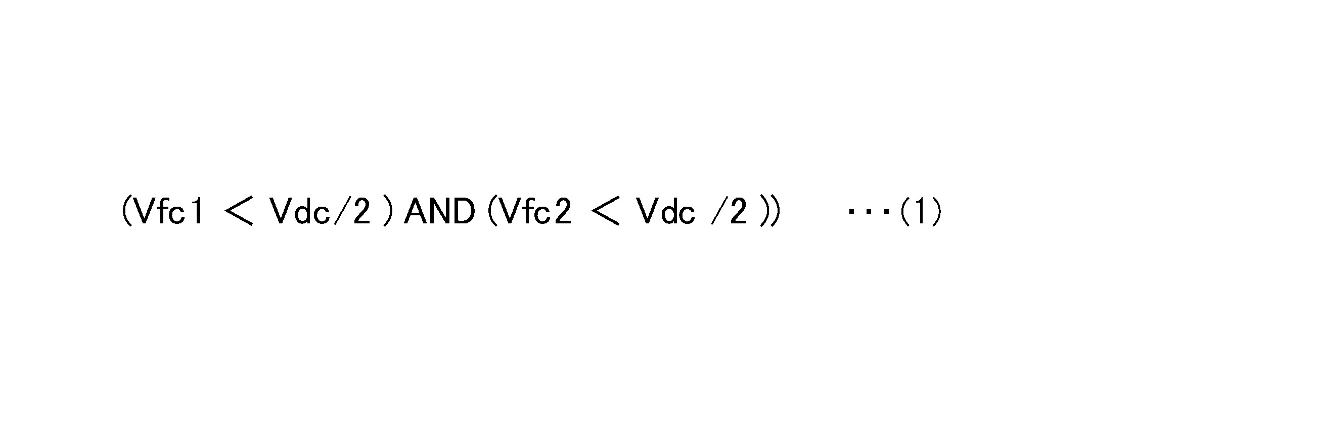
- the switching pattern shown in Table 1 below the condition shown in the following equation (1) is not satisfied, or the condition shown in the following equation (1) is not satisfied.
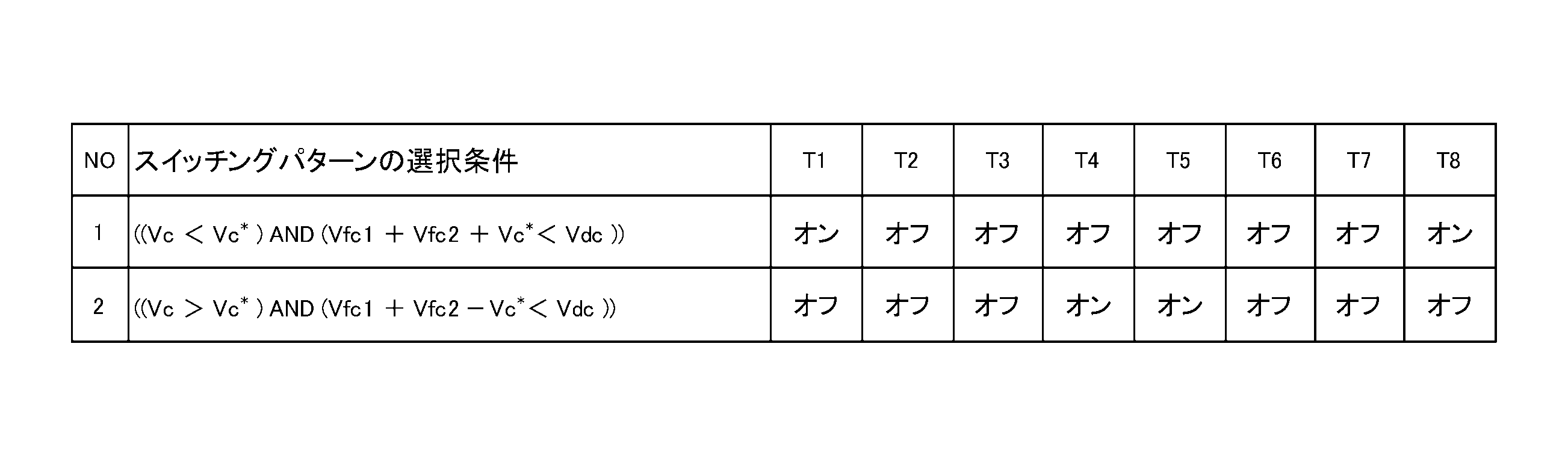
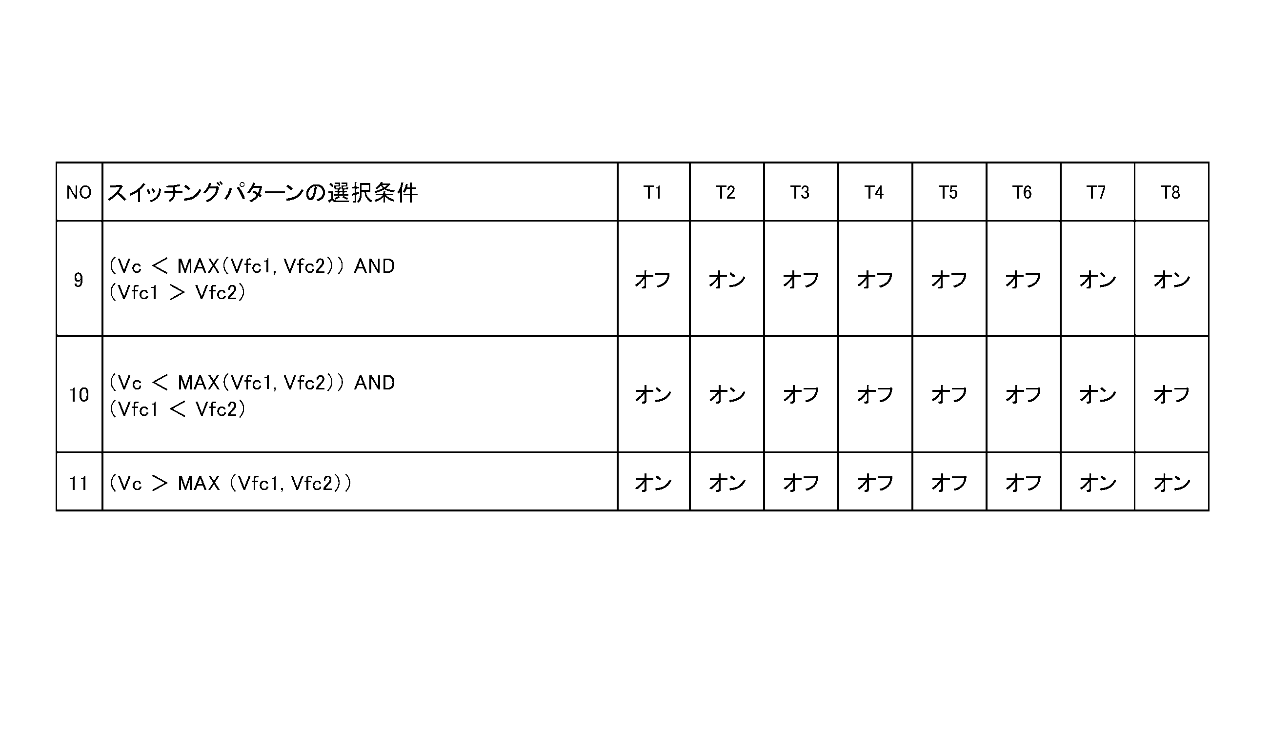
- the switching pattern shown in the following Table 2 and the following equations (1) and (2) are applied. If the conditions shown are not satisfied and the conditions shown in the following equation (3) are satisfied, the first to eighth semiconductor switching elements are turned on or off according to the switching pattern shown in Table 3 below, and the following equations (1) to When all the conditions shown in the equation (3) are not satisfied, all the first to eighth semiconductor switching elements are turned off.
- Vfc1 First flying capacitor voltage
- Vfc2 Second flying capacitor voltage
- Vdc DC voltage source voltage
- Vc Filter capacitor voltage
- Vc * Filter capacitor voltage command values T1 to T8: First to eighth semiconductor switching elements.
- First to Nth units each including a flying capacitor connected between a third semiconductor switching element and a connection point of the fourth semiconductor switching element, and each.
- the first to Nth reactors one end of which is connected to the connection points of the second and third semiconductor switching elements of the unit, and the other ends of the first to Nth reactors, respectively.
- a filter reactor that includes a filter capacitor with the lowest flying capacitor voltage and the second lowest unit as the first unit and the second unit, one end of which is connected to the first unit and the second unit. Is a first and second filter reactor, and the filter capacitor voltage of the filter capacitor connected between the other ends of the first and second filter reactors is Vc.
- the FC type 3-level power conversion device it is possible to charge both the flying capacitor and the filter capacitor without outputting a current to the outside of the device.
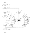
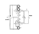
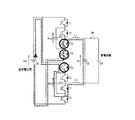
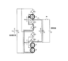
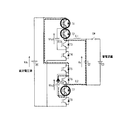
- FIG. The flowchart which shows the procedure of the charging process in Embodiment 1. The figure which shows the current path in each switching pattern.
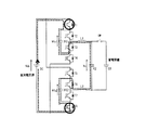
- the figure which shows the current path in the switching pattern of Embodiment 5 No1).
- the figure which shows the current path in the switching pattern of Embodiment 5 No.
- the figure which shows the current path in the switching pattern of Embodiment 5 (No4).
- the figure which shows the current path in the switching pattern of Embodiment 5 (No5).
- the figure which shows the current path in the switching pattern of Embodiment 5 (No. 6).
- the figure which shows the current path in the switching pattern of Embodiment 5 (No. 7).
- the figure which shows the current path in the switching pattern of Embodiment 5 (No. 8).
- the figure which shows the current path in the switching pattern of Embodiment 5 (No. 9).
- the figure which shows the current path in the switching pattern of Embodiment 5 (No10).
- the figure which shows the current path in the switching pattern of Embodiment 5 (No11).
- the circuit diagram which shows the FC type 3 level power conversion apparatus in Embodiment 7. The circuit diagram which shows the conventional FC type 3 level chopper circuit.
- FIG. 1 shows the circuit configuration of the FC type 3 level power converter (FC type 3 level chopper circuit) in the first embodiment.
- a high-voltage side filter capacitor C1 is connected in parallel to the DC voltage source DC.
- the first to fourth semiconductor switching elements T1 to T4 are sequentially connected in series between the positive electrode and the negative electrode of the filter capacitor C1 on the high voltage side.
- the flying capacitor FC is connected between the connection points of the first and second semiconductor switching elements T1 and T2 and the connection points of the third and fourth semiconductor switching elements T3 and T4.
- One end of the filter reactor L is connected to the connection points of the second and third semiconductor switching elements T2 and T3.
- a low-voltage side filter capacitor C2 is connected between the other end of the filter reactor L and the negative electrode of the high-voltage side filter capacitor C1.
- the connection point between the filter reactor L and the filter capacitor C2 on the low voltage side and the negative electrode of the DC voltage source DC serve as output terminals.
- the high-voltage side filter capacitor voltage is Va
- the low-voltage side filter capacitor voltage is Vb
- the flying capacitor voltage is Vfc.
- the DC voltage source DC is connected to the high voltage side and the flying capacitor FC and the filter capacitor C2 on the low voltage side are charged from the DC voltage source DC.
- the power converter consisting of the chopper circuit and the LC filter and the load are separated.
- FIG. 2 is a flowchart showing the procedure of the charging process in the first embodiment.
- the branch goes down, and if the condition is not satisfied, the branch goes right.
- the predetermined value ⁇ 0 in the determination.
- the predetermined value ⁇ will be described later.
- the flying capacitor FC and the low-voltage side filter capacitor C2 are charged according to the following procedures (S1 to S15).
- Vb ⁇ Vb * that is, both the flying capacitor FC and the low-voltage side filter capacitor C2
- Va> Vfc + Vb the process proceeds to S5 and the first semiconductor switching element T1 is turned on.
- Va ⁇ Vfc + Vb after shifting to S6 and turning on the first semiconductor switching element T1 and the second semiconductor switching element T2, shifting to S5 and turning off the second semiconductor switching element T2 and only the first semiconductor switching element T1. Is turned on.
- Vb> Vfc the process proceeds to S8 and the fourth semiconductor switching element T4 is turned on.
- Vb ⁇ Vfc the process shifts to S9 to turn on the third semiconductor switching element T3 and the fourth semiconductor switching element T4, then shifts to S8 to turn off the third semiconductor switching element T3 and turns off the fourth semiconductor switching element T4. Turn on only.
- the gates of all semiconductor switching elements are turned off.
- the gate ON time or standby time is assumed to be short (about 10 ⁇ s).
- the above operation is repeated until the start of operation at a frequency such as 1 ms interval where the thermal duty of the semiconductor switching element and the filter reactor does not become a problem.
- FIG. 3 shows the current path in each switching pattern.
- the first semiconductor switching element T1 is turned on in S5
- the path (C1 ⁇ T1 ⁇ FC ⁇ T3 ⁇ L ⁇ C2) of FIG. 3 (b) is turned on. Charges the flying capacitor FC and the low-voltage side filter capacitor C2.
- the fourth semiconductor switching element T4 is turned on in S8, and the path (C2 ⁇ L ⁇ ) in FIG. 3 (d) is turned on.
- a current is passed through T2 ⁇ FC ⁇ T4) to charge the flying capacitor FC from the filter capacitor C2 on the low voltage side.
- the flying capacitor voltage Vfc is sufficient and only the low-voltage side filter capacitor C2 is to be charged, if Vfc> Vb, the second semiconductor switching element T2 is turned on in S12, and the path (FC ⁇ T2 ⁇ ) in FIG. 3 (e) is turned on. A current is passed through L ⁇ C2 ⁇ T4) to charge the low voltage side filter capacitor C2 from the flying capacitor FC.
- the flying capacitor voltage Vfc can be charged to Va / 2
- the low voltage side filter capacitor voltage Vb can be charged to the filter capacitor voltage command value Vb *.
- the flying capacitor FC and the filter capacitor C2 on the low voltage side can be charged from the high voltage side in the FC type 3 level power converter (FC type 3 level chopper circuit).
- the first embodiment can be applied with the load connected, and the current flowing through the load can be minimized by shortening the gate ON time.
- the flying capacitor FC and the low-voltage side filter capacitor C2 can be charged without separately preparing a pre-charging circuit.
- FIG. 4 shows the circuit configuration of the FC type 3 level power conversion device (FC type 3 level chopper circuit) in the second embodiment.
- the DC voltage source DC is connected in parallel to the low voltage side filter capacitor C2, and the DC voltage source DC connected in parallel to the high voltage side filter capacitor C1 is deleted.
- Others are the same as in the first embodiment (FIG. 1).
- the flying capacitor FC and the high-voltage side filter capacitor C1 are charged from the DC voltage source DC.
- the load is separated.
- the flying capacitor voltage Vfc and Va / 2 which is 1/2 of the high-voltage side filter capacitor voltage Va, are compared.
- Va> Va * that is, when it is necessary to charge only the flying capacitor FC, shift to S4 and compare the filter capacitor voltage Va on the high voltage side with Vfc + Vb. If Va> Vfc + Vb, the process proceeds to S5 and the first semiconductor switching element T1 is turned on.
- Vb> Vfc the process shifts to S8 and the fourth semiconductor switching element T4 is turned on.
- Vb ⁇ Vfc after shifting to S9 and turning on the third semiconductor switching element T3 and the fourth semiconductor switching element T4, shifting to S8 and turning off the third semiconductor switching element T3 and only the fourth semiconductor switching element T4. Is turned on.
- Va ⁇ Va * that is, when it is necessary to charge only the high-voltage side filter capacitor C1, the process shifts to S18 and Vfc + Vb is compared with the high-voltage side filter capacitor voltage Va.
- Vfc + Vb> Va When Vfc + Vb> Va, the process shifts to S19 and the third semiconductor switching element T3 is turned on. In the case of Vfc + Vb ⁇ Va, after shifting to S20 and turning on the third semiconductor switching element T3 and the fourth semiconductor switching element T4, shifting to S19 and turning off the fourth semiconductor switching element T4 and only the third semiconductor switching element T3. Is turned on.
- the second embodiment also assumes that the gate ON time or standby time is short (about 10 ⁇ s). The above operation is repeated until the start of operation.
- Vb ⁇ Vb * (when it is desired to charge the filter capacitor C2 on the low voltage side)" of S3 and S10 in the first embodiment is set to "Va> Va *" in S16 and S17. If you want to discharge the filter capacitor C1 on the high voltage side) ”. That is, in the flowchart of FIG. 5, the direction of the inequality sign may be changed in the second determination.
- the fourth semiconductor switching element T4 is also turned on and the current flows through the path shown in FIG. 3C, and then the current flows.
- the fourth semiconductor switching element T4 is turned off and the current path is shown in FIG. 3 (f).
- the flying capacitor FC and the filter capacitor C1 on the high voltage side can be charged from the low voltage side. ..
- Other effects are the same as in the first embodiment, but in the second embodiment, a precharging circuit for the filter capacitor C1 on the high voltage side is required. The pre-charging circuit of the flying capacitor FC is unnecessary.
- FIG. 6 shows the circuit configuration of the third embodiment.
- the third embodiment has a configuration in which the positive electrode side of the high-voltage side filter capacitor C1 and the low-voltage side filter capacitor C2 have a common potential.
- the semiconductor switching elements are the fourth semiconductor switching element T4, the third semiconductor switching element T3, the second semiconductor switching element T2, and the first semiconductor switching element T1 in order from the positive side. Others are the same as those of the first embodiment or the second embodiment.
- the flying capacitor FC and the low-voltage side filter capacitor C2 are charged in the same procedure as in the first embodiment.
- the flying capacitor FC and the high-voltage side filter capacitor C2 are charged in the same procedure as in the second embodiment.
- the negative electrode side of the high voltage side filter capacitor C1 and the low voltage side filter capacitor C2 have a common potential.
- FIG. 6 a circuit configuration in which the positive electrode side has a common potential is also possible.
- the flying capacitor FC and the high-voltage side filter capacitor C1 or the low-voltage side can be obtained in exactly the same procedure as in the first and second embodiments for the circuit configuration of FIG.
- the filter capacitor C2 can be charged and discharged.
- the same effect as that of the first and second embodiments can be obtained even in the FC type 3 level power conversion device (FC type 3 level chopper circuit) in which the positive electrode side has a common potential. ..
- the predetermined value ⁇ > 0 is set in the voltage comparison (S4, S7, S11, S18) of the flowcharts of FIGS. 2 and 5.
- the voltage Va-Vfc-Vb> 0 applied to the filter reactor L is larger than zero but very small, and the charging current flows but charging takes time. To prevent this, set a predetermined value ⁇ > 0.
- the voltage Va-Vfc-Vb applied to the filter reactor L can be surely made larger than the predetermined value ⁇ .
- Va> Vfc + Vb + ⁇ If Va> Vfc + Vb + ⁇ is not satisfied, the voltage applied to the filter reactor L becomes Va-Vb by turning on the first semiconductor switching element T1 and the second semiconductor switching element T2 together, and a large charging current is passed to charge the charging time. Can be shortened.
- the value of the predetermined value ⁇ As a guideline for the value of the predetermined value ⁇ , it is about 10% to 30% of the rated value (withstand voltage value) of the filter capacitor voltage on the high voltage side, although it depends on the size of the filter reactor L.
- the value of the predetermined value ⁇ is made variable, and immediately after the device is started up, the predetermined value ⁇ is increased to shorten the time until charging is completed, and once the flying capacitor FC and the high-voltage side filter capacitor C1 or the low-voltage side filter capacitor C2 When charging is completed, the predetermined value ⁇ can be reduced to reduce the charging current, improve the accuracy of voltage control, and reduce the thermal duty of the device parts.
- the time required for charging the flying capacitor FC and the filter capacitor C can be shortened.
- the DC voltage source DC and the first and second flying capacitors are “standby”.
- a method of maintaining the charging and charging states of the first and second flying capacitors FC1 and FC2 and the filter capacitor C2 by turning on / off the semiconductor switching element according to the charging state of the FC1 and FC2 and the filter capacitor C2 will be described. To do.
- FIG. 7 shows a schematic diagram of the FC type 3-level power converter (FC-type 3-level converter) according to the fifth embodiment.
- the load is the power storage device C3.
- FC type 3-level power converter (FC-type 3-level converter) shown in FIG. 7 will be described.
- the first unit 1 and the second unit 2 are connected to the DC voltage source DC.
- the first to fourth semiconductor switching elements T1 to T4 are sequentially connected in series between the positive electrode and the negative electrode of the DC voltage source DC.
- the first flying capacitor FC1 is connected between the connection points of the first and second semiconductor switching elements T1 and T2 and the connection points of the third and fourth semiconductor switching elements T3 and T4.
- the connection points of the second and third semiconductor switching elements T2 and T3 serve as output terminals of the first unit 1.
- the fifth to eighth semiconductor switching elements T5 to T8 are sequentially connected in series between the positive electrode and the negative electrode of the DC voltage source DC.
- the second flying capacitor FC2 is connected between the connection points of the fifth and sixth semiconductor switching elements T5 and T6 and the connection points of the seventh and eighth semiconductor switching elements T7 and T8.
- the connection points of the sixth and seventh semiconductor switching elements T6 and T7 serve as output terminals of the second unit.
- One ends of the first and second filter reactors L1 and L2 are connected to the output terminals of the first unit 1 and the second unit 2, respectively.
- a filter capacitor C2 is connected between the other ends of the first and second filter reactors L1 and L2.
- a power storage device C3 is connected in parallel to the filter capacitor C2.
- a switch SW is connected between the filter capacitor C2 and the power storage device C3.
- the filter capacitor voltage command value Vc * of the filter capacitor C2 is set so as to match the voltage value of the power storage device C3.
- Vc * ⁇ 0.
- Vc indicates the filter capacitor voltage
- Vfc1 indicates the first flying capacitor voltage
- Vfc2 indicates the second flying capacitor voltage
- Vdc indicates the DC voltage source voltage
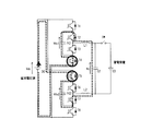
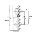
- the switching pattern shown in FIG. 8 is used for No. 1 in Table 1, and the switching pattern shown in FIG. 9 is used for No. 2.
- the circles indicate that the semiconductor switching element is in the ON state.
- the broken line represents the current direction, and the arrow direction is positive.
- the current flows in the path of DC ⁇ T1 ⁇ FC1 ⁇ T3 ⁇ L1 ⁇ C2 ⁇ L2 ⁇ T6 ⁇ FC2 ⁇ T8.
- the current flows in the path of DC ⁇ T5 ⁇ FC2 ⁇ T7 ⁇ L2 ⁇ C2 ⁇ L1 ⁇ T2 ⁇ FC1 ⁇ T4.
- conditional expression of (1) above is not satisfied, or when the conditional expression of (1) above is satisfied but the selection conditions of Table 1 are not satisfied, and the conditional expression of (2) below is satisfied. That is, only one of the first and second flying capacitors FC1 and FC2 needs to be charged, or the voltages of the first and second flying capacitors FC1 and FC2 and the filter capacitor C2 do not reach the command value. However, if the total voltage of the first and second flying capacitors FC1 and FC2 and the filter capacitor C2 is higher than the DC voltage Vdc and the first and second flying capacitors FC1 and FC2 cannot be charged at the same time, the DC voltage source DC, Alternatively, the filter capacitor C2 is charged from the first flying capacitor FC1 or the second flying capacitor FC2, whichever has the lower voltage value.
- the switching pattern turns each semiconductor switching element on / off according to Table 2.
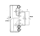
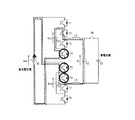
- FIG. 10 for No. 3 in Table 2
- FIG. 11 for No. 4, FIG. 12 for No. 5, FIG. 13 for No. 6, FIG. 14 for No. 7, and FIG. 15 for No. 8. ..
- circles indicate that the semiconductor switching element is in the on state.
- the broken line represents the current direction, and the arrow direction is positive.
- the first flying capacitor FC1 or the second flying capacitor FC2 is charged, the filter capacitor C2 is charged at No4 and No7 in Table 2, and discharged at No3, No5, No6, and No8.
- the switching pattern turns each semiconductor switching element on / off according to Table 3.
- FIG. 16 for No. 9 in Table 3, FIG. 17 for No. 10, and FIG. 18 for No. 11.
- circles indicate that the semiconductor switching element is in the ON state.
- the broken line represents the current direction, and the arrow direction is positive.
- the filter capacitor C2 is charged, and No. 9 (FIG. 16) in Table 3 discharges the first flying capacitor FC1 and No. 10 (FIG. 17) discharges the second flying capacitor FC2.
- the on-time of the semiconductor switching element should be short (about 10 ⁇ s) because the device may be damaged due to overcurrent depending on the value of the filter reactor.
- first flying capacitor voltage Vfc1 and the second flying capacitor voltage Vfc2 are within the range of E / 2 ⁇ tolerance, and the filter capacitor voltage Vc is within the range of the filter capacitor voltage command value Vc * ⁇ tolerance, once , Turn off all the semiconductor switching elements and finish charging.
- the fifth embodiment after the first and second flying capacitor voltages Vfc1 and Vfc2 are established at E / 2, power can be supplied to a load such as the power storage device C3. As a result, the output voltage and waveform distortion are reduced, and a highly accurate voltage can be applied to the load from the initial state of load feeding. Further, since the filter capacitor voltage Vc matches the voltage value of the power storage device C3, unnecessary inrush current when the switch SW is turned on is reduced.
- FIG. 19 shows the configuration of the FC type 3-level power converter (FC-type 3-level converter) of the sixth embodiment.
- the first and second flying capacitors FC1 and FC2 and the first to eighth semiconductor switching elements T1 to T8 in FIG. 7 are changed as shown in FIG. That is, by exchanging the first and second units 1 and 2, the equations (1), (2), (3) and Table 1, Table 2, and Table 3 of the fifth embodiment can be applied. The same effect as in 5 can be obtained.
- N is set to 3.
- each unit four semiconductor switching elements are connected in series between the positive electrode and the negative electrode of the DC voltage source DC.
- a flying capacitor is connected between the connection point between the first semiconductor switching element and the second semiconductor switching element and the connection point between the third semiconductor switching element and the fourth semiconductor switching element.
- One end of the 1st to Nth filter reactors is connected to the connection point between the 2nd semiconductor switching element and the 3rd semiconductor switching element of each unit.
- a filter capacitor is connected between the other ends of the first to Nth filter reactors.
- the unit with the lowest flying capacitor voltage and the unit with the second lowest flying capacitor voltage are referred to as the first and second units 1 and 2.
- the filter reactors having one end connected to the first and second units 1 and 2 are referred to as the first and second filter reactors L1 and L2.
- Vc be the flying capacitor voltage of the filter capacitor C connected between the other ends of the first and second filter reactors L1 and L2.
- the DC voltage source DC may be a DC power supply or a DC capacitor.
Landscapes
- Engineering & Computer Science (AREA)
- Power Engineering (AREA)
- Physics & Mathematics (AREA)
- Electromagnetism (AREA)
- Dc-Dc Converters (AREA)
- Inverter Devices (AREA)
- Power Conversion In General (AREA)
Abstract
フライングキャパシタ電圧Vfcと高圧側のフィルタコンデンサ電圧Vaの1/2との比較、および、高圧側のフィルタコンデンサ電圧Vaとフライングキャパシタ電圧Vfc+低圧側のフィルタコンデンサ電圧Vbとの比較、フライングキャパシタ電圧Vfcと低圧側のフィルタコンデンサ電圧Vbとの比較、および、低圧側のフィルタコンデンサ電圧Vbまたは高圧側のフィルタコンデンサ電圧Vaとフィルタコンデンサ電圧指令値との比較、に基づいて、第1~第4半導体スイッチング素子T1~T4をONまたはOFFしてフィルタリアクトルLを含む経路に電流を流し、フライングキャパシタFCおよび低圧側のフィルタコンデンサC2または高圧側のフィルタコンデンサC1を所定の値に充電する。これにより、FC型3レベル電力変換装置において、装置外部に電流を出力することなくフライングキャパシタとフィルタコンデンサの両方を充電する。
Description
本発明は、フライングキャパシタ(FC)型3レベル電力変換装置において、フライングキャパシタおよびフィルタコンデンサの電圧制御に関する。
図21に特許文献1記載のFC型3レベルチョッパ回路を示し、図22に、複数のユニットを有し、差動出力可能なFC型3レベル変換器の構成例を示す。本明細書では、図21に示すようなFC型3レベルチョッパ回路と、図22に示すようなFC型3レベル変換器を含めて、FC型3レベル電力変換装置と称する。
FC型3レベル電力変換装置は2レベルに比べ出力電圧リプルが半分である。また、遮断電圧も半分であるため半導体スイッチング素子のスイッチング損失が減少し、スイッチング周波数を上げやすくなる。この特長は、高効率や高い応答速度、低リプルが要求される装置に適している。
FC型3レベル電力変換装置を正常に動作させるためには、フライングキャパシタ電圧Vfc,Vfc1,Vfc2を直流電圧源電圧の半分に制御する必要がある。フライングキャパシタ電圧Vfc,Vfc1,Vfc2にずれが生じると、一部の半導体スイッチング素子に過大な電圧がかかり、出力電圧に重畳するリプルが大きくなり出力電圧や出力電流の波形がひずみ、周囲の装置の誤動作やフィルタのリアクトル、フィルタコンデンサおよびトランスの過熱といった問題が発生する。
特許文献2,3にはFC型3レベルインバータ向けのFC電圧制御法が開示されており、FC型3レベルチョッパ回路にもそのまま適用することができる。
差動出力可能なLCフィルタを有するFC型3レベル変換器は、直流電圧源電圧VdcをEとしたとき、第1~第8半導体スイッチング素子T1~T8のオンまたはオフの動作によって、第1,第2フライングキャパシタ電圧Vfc1、Vfc2をE/2(Vdcの半分)に制御しつつ、3レベルの電圧(E,E/2,0)を第2,第3半導体スイッチング素子T2,T3の接続点、第6,第7半導体スイッチング素子T6,T7の接続点より出力して負荷に印加する。
FC型3レベル変換器の詳細は、一般文献や特許文献5に開示されている。
特許文献2,3を用いてフライングキャパシタ電圧を制御するためには、装置が電流を出力している必要がある。そのため、装置が停止している間は自然放電によりフライングキャパシタ電圧が減少してしまう。また、運転前にあらかじめフライングキャパシタ電圧を直流電圧の半分程度に充電する手段が別途必要になる。
また、一般的な電力変換装置にはスイッチングリプルの除去を目的としてフィルタコンデンサが接続されている。例えば装置にバッテリーを接続する場合、バッテリーからフィルタコンデンサに突入電流が流れてしまう。これを防止するため、あらかじめフィルタコンデンサをバッテリーと同じ電圧に充電する必要がある。特許文献4ではフィルタコンデンサの接続を想定していないため、フィルタコンデンサの充電を行うことができない。
以上示したようなことから、FC型3レベル電力変換装置において、装置外部に電流を出力することなくフライングキャパシタとフィルタコンデンサの両方を充電することが課題となる。
本発明は、前記従来の問題に鑑み、案出されたもので、その一態様は、高圧側のフィルタコンデンサと、前記高圧側のフィルタコンデンサの正極と負極との間に順次直列接続された第1~第4半導体スイッチング素子と、前記第1,第2半導体スイッチング素子の接続点と前記第3,第4半導体スイッチング素子の接続点との間に接続されたフライングキャパシタと、前記第2,第3半導体スイッチング素子の接続点に一端が接続されたフィルタリアクトルと、前記フィルタリアクトルの他端と前記高圧側のフィルタコンデンサの負極との間に接続された低圧側のフィルタコンデンサと、前記高圧側のフィルタコンデンサ、または、前記低圧側のフィルタコンデンサに対して並列接続された直流電圧源と、を備えたFC型3レベル電力変換装置であって、フライングキャパシタ電圧と高圧側のフィルタコンデンサ電圧の1/2との比較、および、前記高圧側のフィルタコンデンサ電圧と前記フライングキャパシタ電圧+低圧側のフィルタコンデンサ電圧との比較、前記フライングキャパシタ電圧と前記低圧側のフィルタコンデンサ電圧との比較、および、前記低圧側のフィルタコンデンサ電圧または前記高圧側のフィルタコンデンサ電圧とフィルタコンデンサ電圧指令値との比較、に基づいて、前記第1~第4半導体スイッチング素子をONまたはOFFして前記フィルタリアクトルを含む経路に電流を流し、前記フライングキャパシタおよび前記低圧側のフィルタコンデンサまたは前記高圧側のフィルタコンデンサを所定の値に充電することを特徴とする。
また、他の態様として、高圧側のフィルタコンデンサと、前記高圧側のフィルタコンデンサの正極と負極との間に順次直列接続された第4~第1半導体スイッチング素子と、前記第4,第3半導体スイッチング素子の接続点と前記第2,第1半導体スイッチング素子の接続点との間に接続されたフライングキャパシタと、前記第3,第2半導体スイッチング素子の接続点に一端が接続されたフィルタリアクトルと、前記フィルタリアクトルの他端と前記高圧側のフィルタコンデンサの正極との間に接続された低圧側のフィルタコンデンサと、前記高圧側のフィルタコンデンサ、または、前記低圧側のフィルタコンデンサに対して並列接続された直流電圧源と、を備えたFC型3レベル電力変換装置であって、フライングキャパシタ電圧と高圧側のフィルタコンデンサ電圧の1/2との比較、および、前記高圧側のフィルタコンデンサ電圧と前記フライングキャパシタ電圧+低圧側のフィルタコンデンサ電圧との比較、前記フライングキャパシタ電圧と前記低圧側のフィルタコンデンサ電圧との比較、および、前記低圧側のフィルタコンデンサ電圧または前記高圧側のフィルタコンデンサ電圧とフィルタコンデンサ電圧指令値との比較、に基づいて、前記第1~第4半導体スイッチング素子をONまたはOFFして前記フィルタリアクトルを含む経路に電流を流し、前記フライングキャパシタおよび前記低圧側のフィルタコンデンサまたは前記高圧側のフィルタコンデンサを所定の値に充電することを特徴とする。
また、他の態様として、直流電圧源の正極と負極との間に順次直列接続された第1~第4半導体スイッチング素子と、前記第1,第2半導体スイッチング素子の接続点と前記第3,第4半導体スイッチング素子の接続点との間に接続された第1フライングキャパシタと、を有する第1ユニットと、前記直流電圧源の正極と負極との間に順次直列接続された第5~第8半導体スイッチング素子と、前記第5,第6半導体スイッチング素子の接続点と前記第7,第8半導体スイッチング素子の接続点との間に接続された第2フライングキャパシタと、を有する第2ユニットと、前記第2,第3半導体スイッチング素子の接続点に一端が接続された第1フィルタリアクトルと、前記第6,第7半導体スイッチング素子の接続点に一端が接続された第2フィルタリアクトルと、前記第1,第2フィルタリアクトルの他端の間に接続されたフィルタコンデンサと、を備えたFC型3レベル電力変換装置であって、第1,第2フライングキャパシタ電圧と直流電圧源電圧の1/2との比較、および、フィルタコンデンサ電圧とフィルタコンデンサ電圧指令値との比較、および、前記直流電圧源電圧と前記第1フライングキャパシタ電圧+前記第2フライングキャパシタ電圧+前記フィルタコンデンサ電圧指令値との比較、および、前記直流電圧源電圧と前記第1フライングキャパシタ電圧+前記第2フライングキャパシタ電圧-前記フィルタコンデンサ電圧指令値との比較、および、前記第1,第2フライングキャパシタ電圧と前記フィルタコンデンサ電圧との比較、および、前記第1フライングキャパシタ電圧と前記第2フライングキャパシタ電圧との比較に基づいて、前記第1~第8半導体スイッチング素子をONまたはOFFして前記第1,第2フィルタリアクトルを含む経路に電流を流し、前記第1,第2フライングキャパシタおよび前記フィルタコンデンサを所定の値に充電することを特徴とする。
また、他の態様として、前記直流電圧源は前記高圧側のフィルタコンデンサに並列接続されており、Vfc<Va/2、かつ、Vb<Vb*、かつ、Va>Vfc+Vb+αの場合は、前記第1半導体スイッチング素子をON、前記第2,第3,第4半導体スイッチング素子はOFFし、Vfc<Va/2、かつ、Vb<Vb*、かつ、Va≦Vfc+Vb+αの場合は、前記第1,第2半導体スイッチング素子をON、前記第3,第4半導体スイッチング素子はOFFした後、前記第1半導体スイッチング素子をON、前記第2,第3,第4半導体スイッチング素子はOFFし、Vfc<Va/2、かつ、Vb≧Vb*、かつ、Vb>Vfc+αの場合は、前記第4半導体スイッチング素子をON、前記第1,第2,第3半導体スイッチング素子はOFFし、Vfc<Va/2、かつ、Vb≧Vb*、かつ、Vb≦Vfc+αの場合は、前記第3,第4半導体スイッチング素子をON、前記第1,第2半導体スイッチング素子をOFFした後、前記第4半導体スイッチング素子をON、前記第1,第2,第3半導体スイッチング素子をOFFし、Vfc≧Va/2、かつ、Vb<Vb*、かつ、Vfc>Vb+αの場合は、前記第2半導体スイッチング素子をON、前記第1,第3,第4半導体スイッチング素子はOFFし、Vfc≧Va/2、かつ、Vb<Vb*、かつ、Vfc≦Vb+αの場合は、前記第1,第2半導体スイッチング素子をON、前記第3,第4半導体スイッチング素子はOFFした後、前記第2半導体スイッチング素子をON、前記第1,第3,第4半導体スイッチング素子はOFFし、Vfc≧Va/2、かつ、Vb≧Vb*の場合は、前記第1~第4半導体スイッチング素子のOFF状態を維持することを特徴とする。
ただし、Vfc:フライングキャパシタ電圧
Va:高圧側のフィルタコンデンサ電圧
Vb:低圧側のフィルタコンデンサ電圧
Vb*:低圧側のフィルタコンデンサ電圧指令値
α:所定値。
ただし、Vfc:フライングキャパシタ電圧
Va:高圧側のフィルタコンデンサ電圧
Vb:低圧側のフィルタコンデンサ電圧
Vb*:低圧側のフィルタコンデンサ電圧指令値
α:所定値。
また、他の態様として、前記直流電圧源は前記低圧側のフィルタコンデンサに並列接続されており、Vfc<Va/2、かつ、Va>Va*、かつ、Va>Vfc+Vb+αの場合は、前記第1半導体スイッチング素子をON、前記第2,第3,第4半導体スイッチング素子はOFFし、Vfc<Va/2、かつ、Va>Va*、かつ、Va≦Vfc+Vb+αの場合は、前記第1,第2半導体スイッチング素子をON、前記第3,第4半導体スイッチング素子はOFFした後、前記第1半導体スイッチング素子をON、前記第2,第3,第4半導体スイッチング素子はOFFし、Vfc<Va/2、かつ、Va≦Va*、かつ、Vb>Vfc+αの場合は、前記第4半導体スイッチング素子をON、前記第1,第2,第3半導体スイッチング素子はOFFし、Vfc<Va/2、かつ、Va≦Va*、かつ、Vb≦Vfc+αの場合は、前記第3,第4半導体スイッチング素子をON、前記第1,第2半導体スイッチング素子をOFFした後、前記第4半導体スイッチング素子をON、前記第1,第2,第3半導体スイッチング素子をOFFし、Vfc≧Va/2、かつ、Va>Va*の場合は、前記第1~第4半導体スイッチング素子のOFF状態を維持し、Vfc≧Va/2、かつ、Va≦Va*、かつ、Vfc+Vb>Va+αの場合は、前記第3半導体スイッチング素子をON、前記第1,第2,第4半導体スイッチング素子はOFFし、Vfc≧Va/2、かつ、Va≦Va*、かつ、Vfc+Vb≦Va+αの場合は、前記第3,第4半導体スイッチング素子をONし、前記第1,第2半導体スイッチング素子をOFFした後、前記第3半導体スイッチング素子をON、前記第1,第2,第4半導体スイッチング素子をOFFすることを特徴とする。
ただし、Vfc:フライングキャパシタ電圧
Va:高圧側のフィルタコンデンサ電圧
Vb:低圧側のフィルタコンデンサ電圧
Va*:高圧側のフィルタコンデンサ電圧指令値
α:所定値。
ただし、Vfc:フライングキャパシタ電圧
Va:高圧側のフィルタコンデンサ電圧
Vb:低圧側のフィルタコンデンサ電圧
Va*:高圧側のフィルタコンデンサ電圧指令値
α:所定値。
また、他の態様として、α=0とすることを特徴とする。
また、他の態様として、α>0とすることを特徴とする。
また、他の態様として、以下の(1)式に示す条件を満たす場合、以下の表1に示すスイッチングパターン、以下の(1)式に示す条件を満たさずまたは、以下の(1)式の条件および表1の選択条件の両方を同時に満たさず、かつ、以下の(2)式に示す条件を満たす場合、以下の表2に示すスイッチングパターン、以下の(1)式、(2)式に示す条件を満たさず、以下の(3)式に示す条件を満たす場合、以下の表3に示すスイッチングパターンで前記第1~第8半導体スイッチング素子をONまたはOFFし、以下の(1)式~(3)式に示す条件をすべて満たさない場合、前記第1~第8半導体スイッチング素子をすべてOFFすることを特徴とする。




Vfc1:第1フライングキャパシタ電圧
Vfc2:第2フライングキャパシタ電圧
Vdc:直流電圧源電圧
Vc:フィルタコンデンサ電圧
Vc*:フィルタコンデンサ電圧指令値
T1~T8:第1~第8半導体スイッチング素子。
Vfc2:第2フライングキャパシタ電圧
Vdc:直流電圧源電圧
Vc:フィルタコンデンサ電圧
Vc*:フィルタコンデンサ電圧指令値
T1~T8:第1~第8半導体スイッチング素子。
また、他の態様として、前記直流電圧源の正極と負極との間に順次直列接続された4つの半導体スイッチング素子と、1つ目の半導体スイッチング素子と2つ目の半導体スイッチング素子の接続点と3つ目の半導体スイッチング素子と4つ目の半導体スイッチング素子の接続点との間に接続されたフライングキャパシタと、をそれぞれ備えた第1~第Nユニット(N=3以上の整数)と、各ユニットの2つ目の半導体スイッチング素子と3つ目の半導体スイッチング素子の接続点に一端が接続された第1~第Nリアクトルと、前記第1~第Nリアクトルの他端の間にそれぞれ接続されたフィルタコンデンサと、を備え、フライングキャパシタ電圧が最も低いユニットと、2番目に低いユニットを前記第1ユニット、前記第2ユニットとし、前記第1ユニット,第2ユニットに一端が接続されたフィルタリアクトルを第1,第2フィルタリアクトルとし、前記第1,第2フィルタリアクトルの他端の間に接続されたフィルタコンデンサのフィルタコンデンサ電圧をVcとすることを特徴とする。
本発明によれば、FC型3レベル電力変換装置において、装置外部に電流を出力することなくフライングキャパシタとフィルタコンデンサの両方を充電することが可能となる。
以下、本願発明におけるFC型3レベル電力変換装置の実施形態1~7を図1~図20に基づいて詳述する。
[実施形態1]
図1に本実施形態1におけるFC型3レベル電力変換装置(FC型3レベルチョッパ回路)の回路構成を示す。直流電圧源DCには並列に高圧側のフィルタコンデンサC1が接続される。また、高圧側のフィルタコンデンサC1の正極と負極との間には、第1~第4半導体スイッチング素子T1~T4が順次直列接続される。第1,第2半導体スイッチング素子T1,T2の接続点と第3,第4半導体スイッチング素子T3,T4の接続点との間にフライングキャパシタFCが接続される。
図1に本実施形態1におけるFC型3レベル電力変換装置(FC型3レベルチョッパ回路)の回路構成を示す。直流電圧源DCには並列に高圧側のフィルタコンデンサC1が接続される。また、高圧側のフィルタコンデンサC1の正極と負極との間には、第1~第4半導体スイッチング素子T1~T4が順次直列接続される。第1,第2半導体スイッチング素子T1,T2の接続点と第3,第4半導体スイッチング素子T3,T4の接続点との間にフライングキャパシタFCが接続される。
第2,第3半導体スイッチング素子T2,T3の接続点には、フィルタリアクトルLの一端が接続される。フィルタリアクトルLの他端と高圧側のフィルタコンデンサC1の負極との間には低圧側のフィルタコンデンサC2が接続される。フィルタリアクトルLと低圧側のフィルタコンデンサC2の接続点、および、直流電圧源DCの負極が出力端子となる。
ここで、高圧側のフィルタコンデンサ電圧をVa、低圧側のフィルタコンデンサ電圧をVb、フライングキャパシタ電圧をVfcとする。本実施形態1では高圧側に直流電圧源DCが接続され、直流電圧源DCからフライングキャパシタFCと低圧側のフィルタコンデンサC2を充電することを想定している。チョッパ回路とLCフィルタからなる電力変換装置と負荷は切り離された状態とする。
図2は本実施形態1における充電処理の手順を示すフローチャートである。図2のフローチャートにおける判断では、条件を満たしていれば下に、条件を満たさなければ右に分岐する。本実施形態1では、判断における所定値α=0とする。所定値αについては後述する。本実施形態1は以下の手順(S1~S15)によりフライングキャパシタFCと低圧側のフィルタコンデンサC2を充電する。
S1において、直流電圧源電圧(=高圧側のフィルタコンデンサ電圧)Va,低圧側のフィルタコンデンサ電圧Vb,フライングキャパシタ電圧Vfcを検出する。S2において、フライングキャパシタ電圧Vfcと直流電圧源電圧(=高圧側のフィルタコンデンサ電圧)Vaの1/2であるVa/2を比較する。
Vfc<Va/2、すなわち、フライングキャパシタFCを充電する必要がある場合、S3へ移行して低圧側のフィルタコンデンサ電圧Vbとフィルタコンデンサ電圧指令値Vb*を比較する。
Vb<Vb*、すなわち、フライングキャパシタFCと低圧側のフィルタコンデンサC2の両方を充電する必要がある場合、S4へ移行して直流電圧源電圧(高圧側のフィルタコンデンサ電圧)VaとVfc+Vbを比較する。
Va>Vfc+Vbの場合、S5へ移行して第1半導体スイッチング素子T1をONする。Va≦Vfc+Vbの場合、S6へ移行し、第1半導体スイッチング素子T1と第2半導体スイッチング素子T2をONした後、S5へ移行して第2半導体スイッチング素子T2をOFFし第1半導体スイッチング素子T1のみをONする。
S3において、Vb≧Vb*、すなわち、フライングキャパシタFCだけを充電する必要がある場合、S7へ移行して低圧側のフィルタコンデンサ電圧Vbとフライングキャパシタ電圧Vfcを比較する。
Vb>Vfcの場合、S8へ移行し、第4半導体スイッチング素子T4をONする。Vb≦Vfcの場合、S9へ移行して第3半導体スイッチング素子T3と第4半導体スイッチング素子T4をONした後、S8へ移行して第3半導体スイッチング素子T3をOFFし、第4半導体スイッチング素子T4のみをONする。
S2において、Vfc≧Va/2、すなわち、フライングキャパシタFCの充電が不要の場合、S10へ移行し、低圧側のフィルタコンデンサ電圧Vbとフィルタコンデンサ電圧指令値Vb*を比較する。
Vb<Vb*、すなわち、低圧側のフィルタコンデンサC2だけ充電する必要がある場合、S11へ移行し、フライングキャパシタ電圧Vfcと低圧側のフィルタコンデンサ電圧Vbを比較する。
Vfc>Vbの場合、S12へ移行して第2半導体スイッチング素子T2をONする。Vfc≦Vbの場合、S13へ移行して第1半導体スイッチング素子T1と第2半導体スイッチング素子T2をONした後、S12へ移行して第1半導体スイッチング素子T1をOFFし、第2半導体スイッチング素子T2のみをONする。
S10において、Vb≧Vb*、すなわち、フライングキャパシタFCも低圧側のフィルタコンデンサC2も充電不要の場合、S14へ移行し、第1~第4半導体スイッチング素子T1~T4はOFFを維持し、自然放電を促す。
S15では、すべての半導体スイッチング素子のゲートをOFFする。ゲートON時間、または、待機時間は短時間(10μs程度)を想定している。以上の動作を例えば1ms間隔など半導体スイッチング素子やフィルタリアクトルなどの熱責務が問題にならない頻度で運転開始まで繰り返す。
図3に各スイッチングパターンにおける電流経路を示す。フライングキャパシタFCと低圧側のフィルタコンデンサC2を両方とも充電したい場合、S5において、第1半導体スイッチング素子T1をONし、図3(b)の経路(C1→T1→FC→T3→L→C2)で電流を流し、フライングキャパシタFCと低圧側のフィルタコンデンサC2を充電する。
しかし、両方ともある程度充電が進んでいてVfc+Vb≧Vaの場合は、第1半導体スイッチング素子T1だけをONしても電流が流れない。この場合は、S6において、第2半導体スイッチング素子T2も合わせてONして、図3(a)の経路(C1→T1→T2→L→C2)で電流を流し、S5において、第2半導体スイッチング素子T2だけをOFFして、図3(b)の経路で電流を流す。
低圧側のフィルタコンデンサ電圧Vbは十分でフライングキャパシタFCだけを充電したい場合、Vb>Vfcならば、S8において、第4半導体スイッチング素子T4をONし、図3(d)の経路(C2→L→T2→FC→T4)で電流を流し、低圧側のフィルタコンデンサC2からフライングキャパシタFCへ充電する。
Vb≦Vfcならば第4半導体スイッチング素子T4だけをONしても電流は流れないため、S9において、第3半導体スイッチング素子T3も合わせてONして、図3(c)の経路(C2→L→T3→T4)で電流を流し、その後、S8において、第3半導体スイッチング素子T3だけをOFFして図3(d)の経路で電流を流す。
フライングキャパシタ電圧Vfcは十分で低圧側のフィルタコンデンサC2だけを充電したい場合、Vfc>Vbならば、S12において、第2半導体スイッチング素子T2をONし、図3(e)の経路(FC→T2→L→C2→T4)で電流を流し、フライングキャパシタFCから低圧側のフィルタコンデンサC2へ充電する。
Vfc≦Vbならば第2半導体スイッチング素子T2だけをONしても電流は流れないため、S13において、第1半導体スイッチング素子T1も合わせてONして図3(a)の経路(C1→T1→T2→L→C2)で電流を流し、その後、S12において、第1半導体スイッチング素子T1だけをOFFして図3(e)の経路で電流を流す。
フライングキャパシタFCも低圧側のフィルタコンデンサC2も電圧が十分高い場合は、S14において、すべての半導体スイッチング素子のゲートのOFFを維持し、自然放電を促しつつ待機する(S14)。
以上を一定の周期で繰り返し行うことで、フライングキャパシタ電圧VfcをVa/2に、低圧側のフィルタコンデンサ電圧Vbをフィルタコンデンサ電圧指令値Vb*に充電することができる。
以上示したように、本実施形態1によれば、FC型3レベル電力変換装置(FC型3レベルチョッパ回路)において高圧側からフライングキャパシタFCと低圧側のフィルタコンデンサC2を充電することができる。
負荷を切り離した状態で充電することができるため、負荷に電流を流す必要がなく、負荷接続時の突入電流を防止することができる。負荷を接続した状態で本実施形態1を適用することもでき、ゲートON時間を短くすることにより負荷に流れる電流を最小限にすることができる。
本実施形態1は別途予備充電回路を用意することなくフライングキャパシタFCと低圧側のフィルタコンデンサC2を充電することができる。
[実施形態2]
図4に本実施形態2におけるFC型3レベル電力変換装置(FC型3レベルチョッパ回路)の回路構成を示す。本実施形態2では低圧側のフィルタコンデンサC2に対して直流電圧源DCが並列接続され、高圧側のフィルタコンデンサC1に並列接続された直流電圧源DCが削除されている。その他は実施形態1(図1)と同様である。本実施形態2では、直流電圧源DCからフライングキャパシタFCと高圧側のフィルタコンデンサC1を充電することを想定している。本実施形態2においても負荷は切り離された状態とする。
図4に本実施形態2におけるFC型3レベル電力変換装置(FC型3レベルチョッパ回路)の回路構成を示す。本実施形態2では低圧側のフィルタコンデンサC2に対して直流電圧源DCが並列接続され、高圧側のフィルタコンデンサC1に並列接続された直流電圧源DCが削除されている。その他は実施形態1(図1)と同様である。本実施形態2では、直流電圧源DCからフライングキャパシタFCと高圧側のフィルタコンデンサC1を充電することを想定している。本実施形態2においても負荷は切り離された状態とする。
図5に本実施形態2のフローチャートを示す。本実施形態2においても、判断における所定値α=0とする。本実施形態2は以下の手順(S1,S2,S4~S9,S14~S20)によりフライングキャパシタFCと高圧側のフィルタコンデンサC1を充電する。
S1において、高圧側のフィルタコンデンサ電圧Va,直流電圧源電圧(=低圧側のフィルタコンデンサ電圧)Vb,フライングキャパシタ電圧Vfcを検出する。S2において、フライングキャパシタ電圧Vfcと高圧側のフィルタコンデンサ電圧Vaの1/2であるVa/2を比較する。
Vfc<Va/2の場合、すなわち、フライングキャパシタFCを充電する必要がある場合、S16へ移行し、高圧側のフィルタコンデンサ電圧Vaとフィルタコンデンサ電圧指令値Va*を比較する。
Va>Va*、すなわち、フライングキャパシタFCだけを充電する必要がある場合、S4へ移行して高圧側のフィルタコンデンサ電圧VaとVfc+Vbを比較する。Va>Vfc+Vbならば、S5へ移行して第1半導体スイッチング素子T1をONする。
Va≦Vfc+Vbの場合、S6へ移行して第1半導体スイッチング素子T1と第2半導体スイッチング素子T2をONした後、S5へ移行して第2半導体スイッチング素子T2をOFFし第1半導体スイッチング素子T1のみをONする。
Va≦Va*、すなわち、フライングキャパシタFCと高圧側のフィルタコンデンサC1の両方を充電する必要がある場合、S7へ移行して直流電圧源電圧(=低圧側のフィルタコンデンサ電圧)Vbとフライングキャパシタ電圧Vfcを比較する。
Vb>Vfcの場合、S8へ移行して第4半導体スイッチング素子T4をONする。Vb≦Vfcの場合、S9へ移行して第3半導体スイッチング素子T3と第4半導体スイッチング素子T4をONした後、S8へ移行して第3半導体スイッチング素子T3をOFFし第4半導体スイッチング素子T4のみをONする。
S2において、Vfc≧Va/2、すなわち、フライングキャパシタFCの充電が不要ならば、S17へ移行し、高圧側のフィルタコンデンサ電圧Vaとフィルタコンデンサ電圧指令値Va*を比較する。Va>Va*、すなわち、フライングキャパシタFCも高圧側のフィルタコンデンサC1も充電不要ならば、S14へ移行して、第1~第4半導体スイッチング素子T1~T4はOFFを維持し、自然放電を促す。
Va≦Va*、すなわち、高圧側のフィルタコンデンサC1だけ充電する必要がある場合、S18へ移行してVfc+Vbと高圧側のフィルタコンデンサ電圧Vaを比較する。
Vfc+Vb>Vaの場合、S19へ移行して第3半導体スイッチング素子T3をONする。Vfc+Vb≦Vaの場合、S20へ移行して第3半導体スイッチング素子T3と第4半導体スイッチング素子T4をONした後、S19へ移行して第4半導体スイッチング素子T4をOFFし第3半導体スイッチング素子T3のみをONする。
最後に、S15へ移行してすべての半導体スイッチング素子のゲートをOFFする。
本実施形態2もゲートON時間または待機時間は短時間(10μs程度)を想定している。以上の動作を運転開始まで繰り返す。本実施形態2では、予備充電回路などを用いて高圧側のフィルタコンデンサ電圧Vaをあらかじめ直流電圧源電圧(低圧側のフィルタコンデンサ電圧)Vbまで充電する必要がある。
本実施形態2でのスイッチングパターン選択条件として、実施形態1におけるS3,S10の「Vb<Vb*(低圧側のフィルタコンデンサC2を充電したい場合)」をS16,S17において、「Va>Va*(高圧側のフィルタコンデンサC1を放電したい場合)」に置き換えればよい。すなわち、図5のフローチャートにおいて、2番目の判断において不等号の向きを変えればよい。
ただし、実施形態1における「フライングキャパシタ電圧Vfcもフィルタコンデンサ電圧Vbも十分高い場合(S14)」は本実施形態2において「フライングキャパシタ電圧Vfcは十分高いが高圧側のフィルタコンデンサ電圧Vaは充電が必要(S18)」に相当する。そのため、S19において、第3半導体スイッチング素子T3をONして図3(f)の経路(C2→L→T3→FC→T1→C1)で電流を流し、高圧側のフィルタコンデンサC1を充電する。Va≧Vfc+Vbで第3半導体スイッチング素子T3だけをONしても電流が流れない場合は、S20において、第4半導体スイッチング素子T4もONして図3(c)の経路で電流を流し、その後、S19において、第4半導体スイッチング素子T4をOFFして電流経路を図3(f)とする。
一方、実施形態1における「フライングキャパシタ電圧Vfcは十分だが低圧側のフィルタコンデンサ電圧Vbは充電が必要な場合(S10でYesの場合)」は、本実施形態2において「フライングキャパシタ電圧Vfcも高圧側のフィルタコンデンサ電圧Vaも十分高い場合(S17でYesの場合)」に相当するため、すべての半導体スイッチング素子のゲートのOFFを維持して自然放電を促しつつ待機する(S14)。
以上示したように、本実施形態2によれば、FC型3レベル電力変換装置(FC型3レベルチョッパ回路)において、低圧側からフライングキャパシタFCと高圧側のフィルタコンデンサC1を充電することができる。その他の効果は実施形態1と同等だが、実施形態2では高圧側のフィルタコンデンサC1の予備充電回路が必要となる。なお、フライングキャパシタFCの予備充電回路は不要である。
[実施形態3]
図6に本実施形態3の回路構成を示す。本実施形態3は高圧側のフィルタコンデンサC1,低圧側のフィルタコンデンサC2の正極側を共通電位とした構成である。半導体スイッチング素子は、正極側から順に第4半導体スイッチング素子T4,第3半導体スイッチング素子T3,第2半導体スイッチング素子T2,第1半導体スイッチング素子T1とする。その他は実施形態1、または、実施形態2と同様である。
図6に本実施形態3の回路構成を示す。本実施形態3は高圧側のフィルタコンデンサC1,低圧側のフィルタコンデンサC2の正極側を共通電位とした構成である。半導体スイッチング素子は、正極側から順に第4半導体スイッチング素子T4,第3半導体スイッチング素子T3,第2半導体スイッチング素子T2,第1半導体スイッチング素子T1とする。その他は実施形態1、または、実施形態2と同様である。
高圧側のフィルタコンデンサC1に直流電圧源DCが並列接続された場合、実施形態1と同じ手順でフライングキャパシタFC、および、低圧側のフィルタコンデンサC2を充電する。低圧側のフィルタコンデンサC2に直流電圧源DCが並列接続された場合、実施形態2と同じ手順でフライングキャパシタFC、および、高圧側のフィルタコンデンサC2を充電する。
実施形態1,2では高圧側のフィルタコンデンサC1,低圧側のフィルタコンデンサC2の負極側を共通電位とした構成であった。しかし、図6に示すように正極側を共通電位とする回路構成も可能である。本実施形態3は半導体スイッチング素子の接続順を入れ替えることにより、図6の回路構成に対しても実施形態1,2と全く同じ手順でフライングキャパシタFCおよび高圧側のフィルタコンデンサC1、または、低圧側のフィルタコンデンサC2を充放電することが可能となる。
以上示したように、本実施形態3により、正極側を共通電位としたFC型3レベル電力変換装置(FC型3レベルチョッパ回路)においても実施形態1,2と同様の効果を得ることができる。
[実施形態4]
本実施形態4では、図2,図5のフローチャートの電圧比較(S4,S7,S11,S18)において所定値α>0とする。
本実施形態4では、図2,図5のフローチャートの電圧比較(S4,S7,S11,S18)において所定値α>0とする。
例えば、実施形態1においてVfc<Va/2(フライングキャパシタFCを充電したい),Vb<Vb*(低圧側のフィルタコンデンサC2を充電したい)の場合、Va>Vfc+Vbを満たすならば第1半導体スイッチング素子T1だけをONする。
しかし、両者の値が非常に近い場合、フィルタリアクトルLに印加される電圧Va-Vfc-Vb>0は零よりも大きいが非常に小さくなり、充電電流は流れるが充電に時間がかかってしまう。これを防ぐため所定値α>0を設定する。フィルタリアクトルLに印加される電圧Va-Vfc-Vbを所定値αよりも確実に大きくすることができる。
またVa>Vfc+Vb+αを満たさない場合は、第1半導体スイッチング素子T1と第2半導体スイッチング素子T2をあわせてONすることでフィルタリアクトルLに印加する電圧はVa-Vbとなり、大きな充電電流を流し充電時間を短くすることができる。
所定値αの値の目安としては、フィルタリアクトルLの大きさにもよるが高圧側のフィルタコンデンサ電圧の定格値(耐圧値)の10%~30%程度となる。所定値αの値を可変にし、装置の立ち上げ直後は所定値αを大きくして充電完了までの時間を短縮し、いったんフライングキャパシタFCと高圧側のフィルタコンデンサC1または低圧側のフィルタコンデンサC2の充電が完了したら所定値αを小さくすることで充電電流を小さくし電圧制御の精度を向上し装置部品の熱責務を低減することもできる。
以上示したように、本実施形態4によれば、フライングキャパシタFCおよびフィルタコンデンサCの充電にかかる時間を短くすることができる。
[実施形態5]
実施形態5~7は、差動出力可能なLCフィルタを有するFC型3レベル電力変換装置(FC型3レベル変換器)において、「待機中」に直流電圧源DCや第1,第2フライングキャパシタFC1,FC2、フィルタコンデンサC2の充電状態に応じて、半導体スイッチング素子をオン/オフさせることにより、第1,第2フライングキャパシタFC1,FC2やフィルタコンデンサC2の充電および充電状態を維持する方法を説明する。
実施形態5~7は、差動出力可能なLCフィルタを有するFC型3レベル電力変換装置(FC型3レベル変換器)において、「待機中」に直流電圧源DCや第1,第2フライングキャパシタFC1,FC2、フィルタコンデンサC2の充電状態に応じて、半導体スイッチング素子をオン/オフさせることにより、第1,第2フライングキャパシタFC1,FC2やフィルタコンデンサC2の充電および充電状態を維持する方法を説明する。
図7に本実施形態5におけるFC型3レベル電力変換装置(FC型3レベル変換器)の概略図を示す。図7では、負荷を蓄電装置C3としている。まず、図7に示すFC型3レベル電力変換装置(FC型3レベル変換器)について説明する。
図7に示すように、直流電圧源DCには第1ユニット1と第2ユニット2が接続される。第1ユニット1は、直流電圧源DCの正極と負極との間に第1~第4半導体スイッチング素子T1~T4が順次直列接続される。第1,第2半導体スイッチング素子T1,T2の接続点と第3,第4半導体スイッチング素子T3,T4の接続点との間に第1フライングキャパシタFC1が接続される。第2,第3半導体スイッチング素子T2,T3の接続点が第1ユニット1の出力端子となる。
第2ユニット2は、直流電圧源DCの正極と負極との間に第5~第8半導体スイッチング素子T5~T8が順次直列接続される。第5,第6半導体スイッチング素子T5,T6の接続点と第7,第8半導体スイッチング素子T7,T8の接続点との間に第2フライングキャパシタFC2が接続される。第6,第7半導体スイッチング素子T6,T7の接続点が第2ユニットの出力端子となる。
第1ユニット1と第2ユニット2の出力端子には、それぞれ第1,第2フィルタリアクトルL1,L2の一端が接続される。第1,第2フィルタリアクトルL1,L2の他端の間にはフィルタコンデンサC2が接続される。フィルタコンデンサC2には蓄電装置C3が並列接続される。フィルタコンデンサC2と蓄電装置C3の間にはスイッチSWが接続される。
各半導体スイッチング素子がすべてオフの状態のときに、スイッチSWを開いて、FC型3レベル電力変換装置と蓄電装置C3を切り離しておく。フィルタコンデンサC2のフィルタコンデンサ電圧指令値Vc*は、蓄電装置C3の電圧値と一致するように設定する。なお、本実施形態5では、Vc*≧0とする。
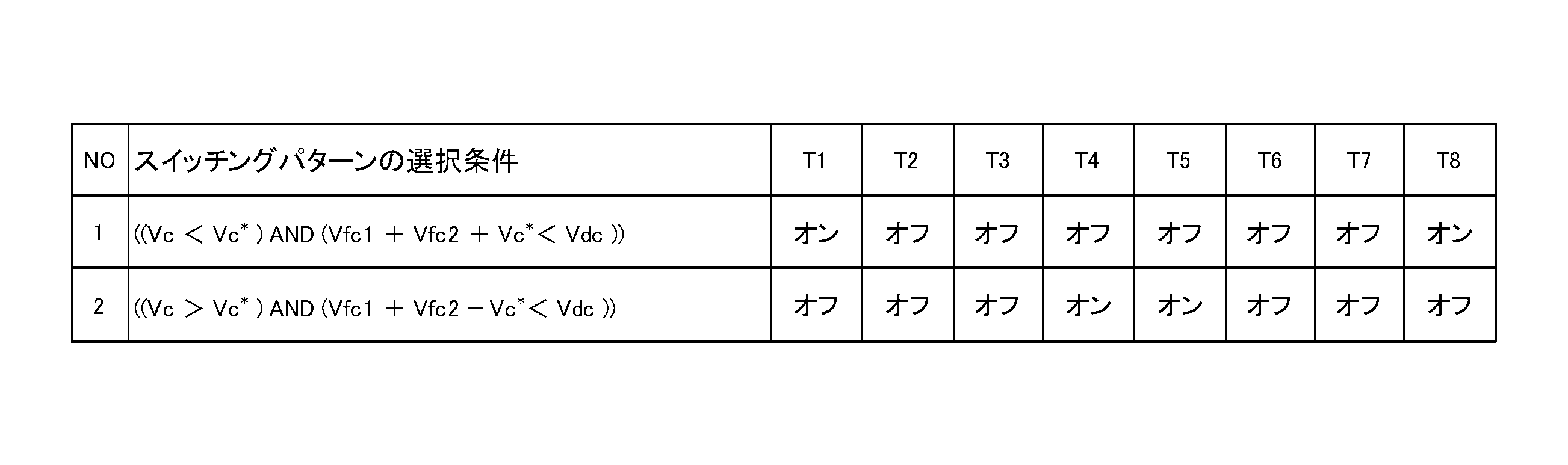
次に、以下の(1)式の条件式を満たす場合、すなわち第1,第2フライングキャパシタFC1,FC2の充電がそれぞれ必要ならば、直流電圧源DCから、第1,第2フライングキャパシタFC1,FC2を同時に充電する。スイッチングパターンは、以下の表1に従って、各半導体スイッチング素子をオン/オフさせる。
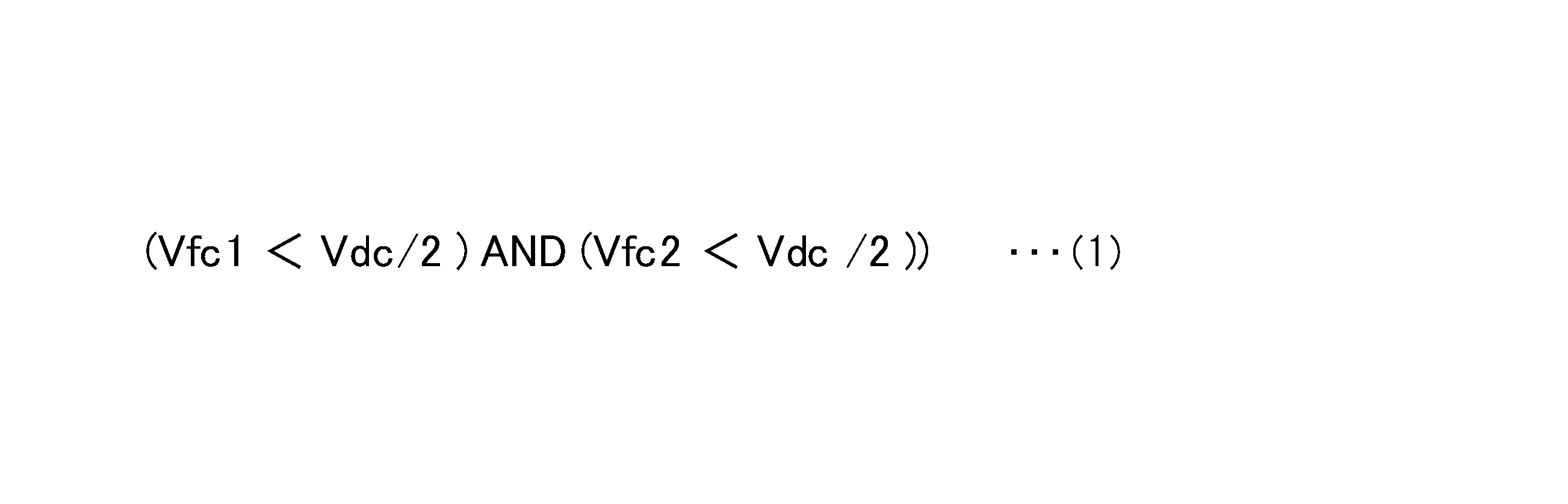

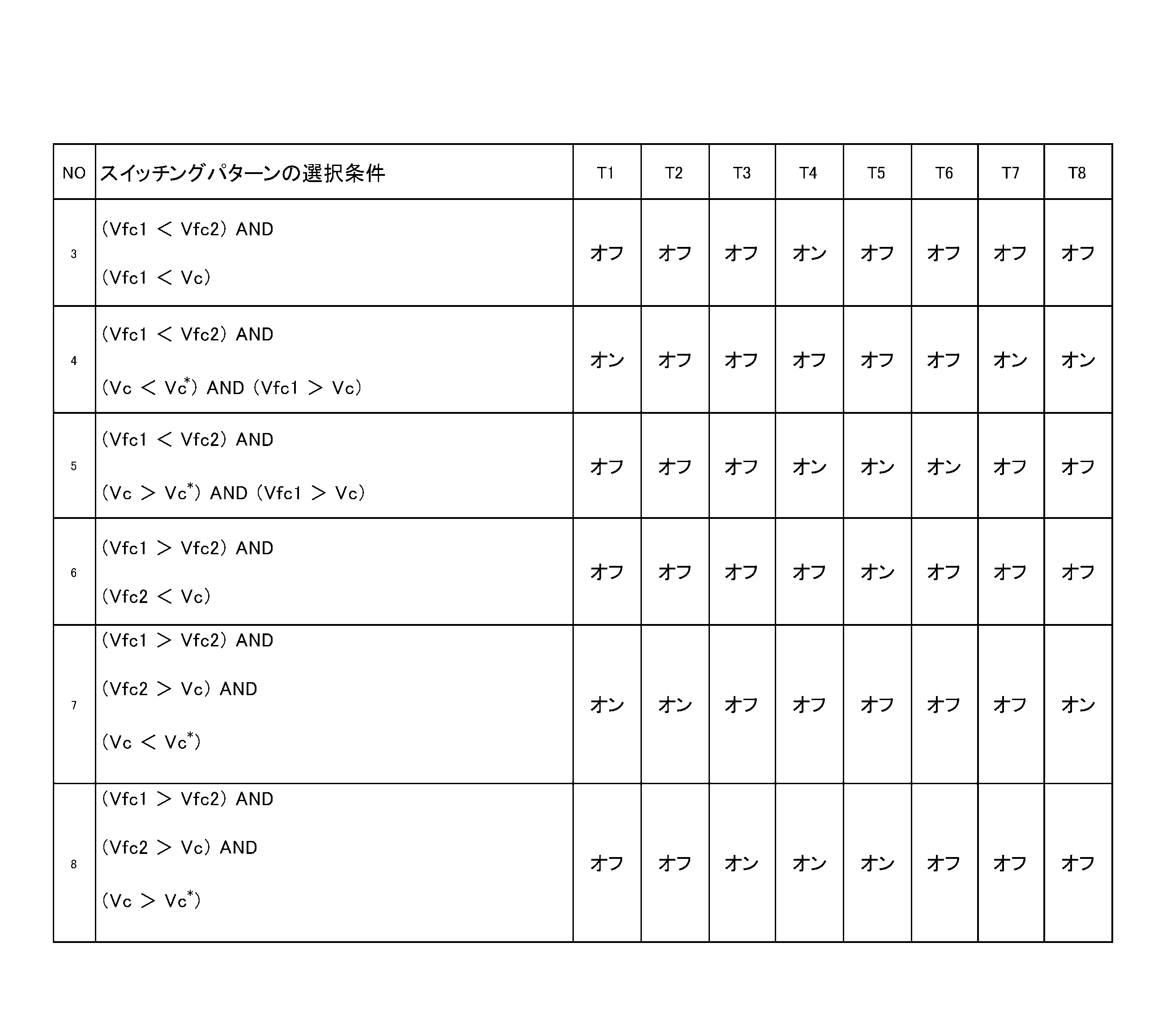
表1において、Vcはフィルタコンデンサ電圧、Vfc1は第1フライングキャパシタ電圧、Vfc2は第2フライングキャパシタ電圧、Vdcは直流電圧源電圧を示す。
表1のNo1の時は図8に示すスイッチングパターンとなり、No2の時は図9に示すスイッチングパターンとなる。図8,図9に示すように、丸印は半導体スイッチング素子がオン状態中を示している。破線は電流方向を表し、矢印方向を正とする。
図8の場合、DC→T1→FC1→T3→L1→C2→L2→T6→FC2→T8の経路で電流が流れる。図9の場合、DC→T5→FC2→T7→L2→C2→L1→T2→FC1→T4の経路で電流が流れる。
これにより、第1フライングキャパシタFC1および第2フライングキャパシタFC2は充電され、フィルタコンデンサC2は表1のNo1(図8)では充電、No2(図9)では放電される。
上記(1)の条件式が満たしていない場合、または上記(1)の条件式を満たしているが表1の選択条件を満たしていない場合、かつ、以下の(2)の条件式を満たす場合、すなわち第1,第2フライングキャパシタFC1,FC2のうち何れか一方のみ充電が必要であるか、または、第1,第2フライングキャパシタFC1,FC2およびフィルタコンデンサC2の電圧が指令値には満たないが、第1,第2フライングキャパシタFC1,FC2およびフィルタコンデンサC2の電圧の合計が直流電圧Vdcより高いために第1,第2フライングキャパシタFC1,FC2を同時に充電できないならば、直流電圧源DC、または、フィルタコンデンサC2から、第1フライングキャパシタFC1、または、第2フライングキャパシタFC2のいずれか電圧値が低い方を充電する。

スイッチングパターンは、表2に従って、各半導体スイッチング素子をオン/オフさせる。
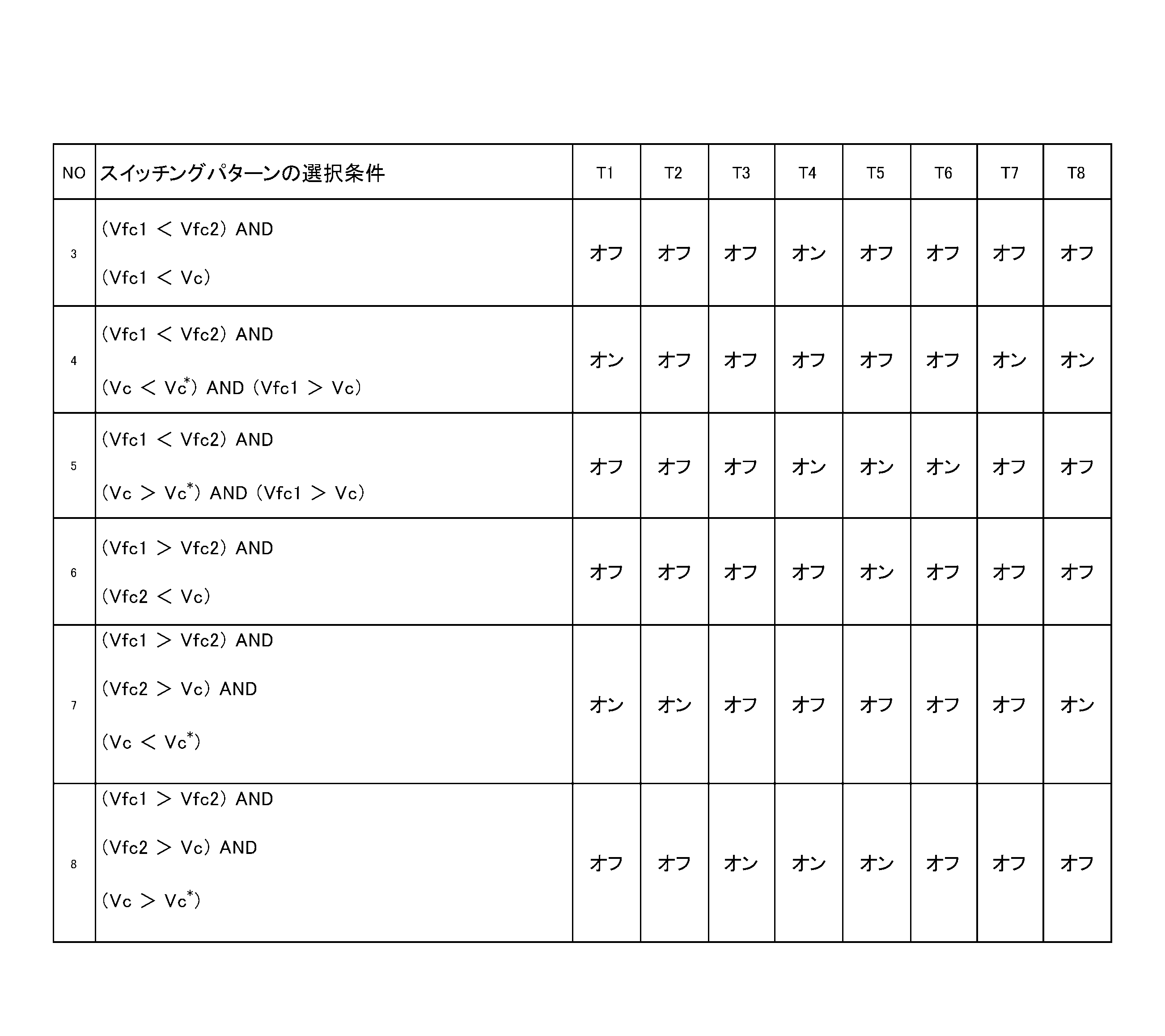
表2のNo3の時は図10、No4の時は図11、No5の時は図12、No6の時は図13、No7の時は図14、No8の時は図15に示すスイッチングパターンとなる。図10、図11、図12、図13、図14、図15に示すように、丸印は半導体スイッチング素子がオン状態中を示している。破線は電流方向を表し、矢印方向を正とする。
図10の場合、C2→L1→T2→FC1→T4→T8→T7→L2の経路で電流が流れる。図11の場合、DC→T1→FC1→T3→L1→C2→L2→T7→T8の経路で電流が流れる。図12の場合、DC→T5→T6→L2→C2→L1→T2→FC1→T4の経路で電流が流れる。図13の場合、C2→L1→T2→T1→T5→FC2→T7→L2の経路で電流が流れる。図14の場合、DC→T1→T2→L1→C2→L2→T6→FC2→T8の経路で電流が流れる。図15の場合、DC→T5→FC2→T7→L2→C2→L1→T3→T4の経路で電流が流れる。
第1フライングキャパシタFC1、または、第2フライングキャパシタFC2は充電され、フィルタコンデンサC2は表2のNo4、No7では充電、No3、No5、No6、No8では放電される。
(1)の条件式および(2)の条件式を満たしておらず、かつ、以下の(3)式の条件式を満たす場合、すなわち、第1,第2フライングキャパシタFC1,FC2の両方が充電されており、フィルタコンデンサC2の充電が必要ならば、直流電圧源DCまたは、第1フライングキャパシタFC1または第2フライングキャパシタFC2のいずれか電圧値が高い方から、フィルタコンデンサC2を充電する。

スイッチングパターンは、表3に従って、各半導体スイッチング素子をオン/オフさせる。
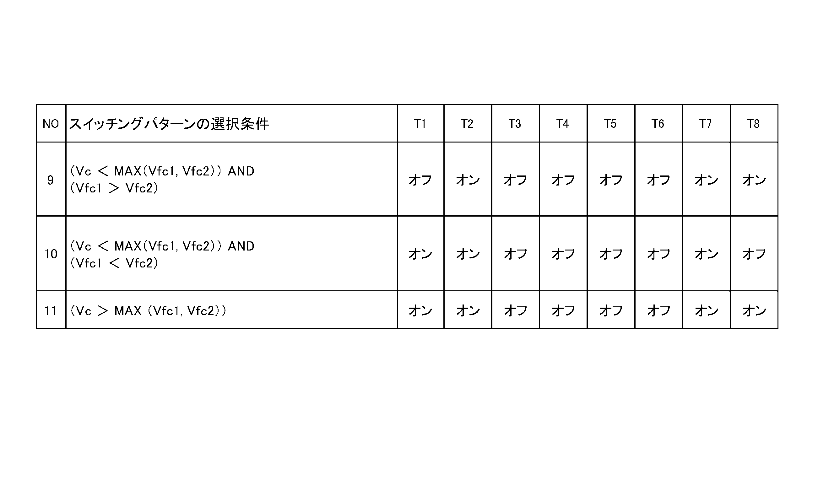
表3のNo9の時は図16、No10の時は図17、No11の時は図18に示すスイッチングパターンとなる。図16,図17,図18に示すように、丸印は半導体スイッチング素子がオン状態中を示している。破線は電流方向を表し、矢印方向を正とする。
図16の場合、FC1→T2→L1→C2→L2→T7→T8→T4の経路で電流が流れる。図17の場合、FC2→T5→T1→T2→L1→C2→L2→T7の経路で電流が流れる。図18の場合、DC→T1→T2→L1→C2→L2→T7→T8の経路で電流が流れる。
フィルタコンデンサC2は充電され、表3のNo9(図16)では第1フライングキャパシタFC1を放電、No10(図17)では第2フライングキャパシタFC2を放電する。
上述した(1)式および(2)式および(3)式を満たさない場合は、一旦、半導体スイッチング素子をすべてオフして、待機中とし、FC型3レベル電力変換装置のインピーダンスで自然放電させる、または外部回路などで放電を行う。
また、半導体スイッチング素子のオン時間は、フィルタリアクトルの値によって、過電流による装置の破損が起こる可能性があるため、オン時間は短時間(10μs程度)とする。
第1フライングキャパシタ電圧Vfc1および第2フライングキャパシタ電圧Vfc2がE/2±許容誤差の範囲内であり、フィルタコンデンサ電圧Vcがフィルタコンデンサ電圧指令値Vc*±許容誤差の範囲内であった場合、一旦、半導体スイッチング素子をすべてオフして、充電を終了する。
その後、スイッチSWをオンしてFC型3レベル電力変換装置と蓄電装置C3を接続した後に、従来技術と同様に給電を行う。この時、第1フライングキャパシタ電圧Vfc1および第2フライングキャパシタ電圧Vfc2の電圧はE/2に充電されており、フィルタコンデンサ電圧Vcは蓄電装置C3の電圧値と一致するため、スイッチSW投入時の突入電流が軽減される。また、給電の初期状態から(E,E/2,0)の負荷電圧を確立することができる。
本実施形態5では、第1,第2フライングキャパシタ電圧Vfc1,Vfc2をE/2に確立してから、蓄電装置C3などの負荷へ給電できる。これにより、出力電圧や波形ひずみが軽減され、負荷給電の初期状態から高精度の電圧を負荷へ印加できるようになる。また、フィルタコンデンサ電圧Vcは蓄電装置C3の電圧値と一致するため、スイッチSW投入時の不要な突入電流が軽減される。
[実施形態6]
本実施形態6では、Vc*<0とした場合、すなわちフィルタコンデンサC2の充電方向を実施形態5の逆としたものである。本実施形態6のFC型3レベル電力変換装置(FC型3レベル変換器)の構成を図19に示す。図7の第1,第2フライングキャパシタFC1,FC2および第1~第8半導体スイッチング素子T1~T8を図19のように変更する。すなわち、第1,第2ユニット1,2を交換することにより、実施形態5の(1)式、(2)式、(3)式および表1、表2、表3が適用でき、実施形態5と同様の効果が得られる。
本実施形態6では、Vc*<0とした場合、すなわちフィルタコンデンサC2の充電方向を実施形態5の逆としたものである。本実施形態6のFC型3レベル電力変換装置(FC型3レベル変換器)の構成を図19に示す。図7の第1,第2フライングキャパシタFC1,FC2および第1~第8半導体スイッチング素子T1~T8を図19のように変更する。すなわち、第1,第2ユニット1,2を交換することにより、実施形態5の(1)式、(2)式、(3)式および表1、表2、表3が適用でき、実施形態5と同様の効果が得られる。
[実施形態7]
本実施形態7では、LCフィルタを有するFC型3レベル電力変換装置のユニットの直列数をN(N=3以上の整数)に拡張したものである。本実施形態7では、図20に示すように、Nを3とした構成としている。
本実施形態7では、LCフィルタを有するFC型3レベル電力変換装置のユニットの直列数をN(N=3以上の整数)に拡張したものである。本実施形態7では、図20に示すように、Nを3とした構成としている。
各ユニットは、直流電圧源DCの正極と負極との間に4つの半導体スイッチング素子が直列接続される。1つ目の半導体スイッチング素子と2つ目の半導体スイッチング素子の接続点と3つ目の半導体スイッチング素子と4つ目の半導体スイッチング素子の接続点との間にフライングキャパシタが接続される。
各ユニットの2つ目の半導体スイッチング素子と3つ目の半導体スイッチング素子の接続点に第1~第Nフィルタリアクトルの一端がそれぞれ接続される。第1~第Nフィルタリアクトルの他端の間にそれぞれフィルタコンデンサが接続される。
フライングキャパシタ電圧の最も低いユニットと2番目に低いユニットを第1,第2ユニット1,2とする。また、第1,第2ユニット1,2に一端が接続されたフィルタリアクトルを第1,第2フィルタリアクトルL1,L2とする。第1,第2フィルタリアクトルL1,L2の他端間に接続されたフィルタコンデンサCのフライングキャパシタ電圧をVcとする。そして、実施形態5の(1)式、(2)式、(3)式および表1、表2、表3を適用することで、実施形態5と同様の効果が得られる。
以上、本発明において、記載された具体例に対してのみ詳細に説明したが、本発明の技術思想の範囲で多彩な変形および修正が可能であることは、当業者にとって明白なことであり、このような変形および修正が特許請求の範囲に属することは当然のことである。
なお、直流電圧源DCは、直流電源としても良く、直流コンデンサとしても良い。
Claims (9)
- 高圧側のフィルタコンデンサと、
前記高圧側のフィルタコンデンサの正極と負極との間に順次直列接続された第1~第4半導体スイッチング素子と、
前記第1,第2半導体スイッチング素子の接続点と前記第3,第4半導体スイッチング素子の接続点との間に接続されたフライングキャパシタと、
前記第2,第3半導体スイッチング素子の接続点に一端が接続されたフィルタリアクトルと、
前記フィルタリアクトルの他端と前記高圧側のフィルタコンデンサの負極との間に接続された低圧側のフィルタコンデンサと、
前記高圧側のフィルタコンデンサ、または、前記低圧側のフィルタコンデンサに対して並列接続された直流電圧源と、を備えたFC型3レベル電力変換装置であって、
フライングキャパシタ電圧と高圧側のフィルタコンデンサ電圧の1/2との比較、および、前記高圧側のフィルタコンデンサ電圧と前記フライングキャパシタ電圧+低圧側のフィルタコンデンサ電圧との比較、前記フライングキャパシタ電圧と前記低圧側のフィルタコンデンサ電圧との比較、および、前記低圧側のフィルタコンデンサ電圧または前記高圧側のフィルタコンデンサ電圧とフィルタコンデンサ電圧指令値との比較、に基づいて、前記第1~第4半導体スイッチング素子をONまたはOFFして前記フィルタリアクトルを含む経路に電流を流し、前記フライングキャパシタおよび前記低圧側のフィルタコンデンサまたは前記高圧側のフィルタコンデンサを所定の値に充電するFC型3レベル電力変換装置。 - 高圧側のフィルタコンデンサと、
前記高圧側のフィルタコンデンサの正極と負極との間に順次直列接続された第4~第1半導体スイッチング素子と、
前記第4,第3半導体スイッチング素子の接続点と前記第2,第1半導体スイッチング素子の接続点との間に接続されたフライングキャパシタと、
前記第3,第2半導体スイッチング素子の接続点に一端が接続されたフィルタリアクトルと、
前記フィルタリアクトルの他端と前記高圧側のフィルタコンデンサの正極との間に接続された低圧側のフィルタコンデンサと、
前記高圧側のフィルタコンデンサ、または、前記低圧側のフィルタコンデンサに対して並列接続された直流電圧源と、を備えたFC型3レベル電力変換装置であって、
フライングキャパシタ電圧と高圧側のフィルタコンデンサ電圧の1/2との比較、および、前記高圧側のフィルタコンデンサ電圧と前記フライングキャパシタ電圧+低圧側のフィルタコンデンサ電圧との比較、前記フライングキャパシタ電圧と前記低圧側のフィルタコンデンサ電圧との比較、および、前記低圧側のフィルタコンデンサ電圧または前記高圧側のフィルタコンデンサ電圧とフィルタコンデンサ電圧指令値との比較、に基づいて、前記第1~第4半導体スイッチング素子をONまたはOFFして前記フィルタリアクトルを含む経路に電流を流し、前記フライングキャパシタおよび前記低圧側のフィルタコンデンサまたは前記高圧側のフィルタコンデンサを所定の値に充電するFC型3レベル電力変換装置。 - 直流電圧源の正極と負極との間に順次直列接続された第1~第4半導体スイッチング素子と、前記第1,第2半導体スイッチング素子の接続点と前記第3,第4半導体スイッチング素子の接続点との間に接続された第1フライングキャパシタと、を有する第1ユニットと、
前記直流電圧源の正極と負極との間に順次直列接続された第5~第8半導体スイッチング素子と、前記第5,第6半導体スイッチング素子の接続点と前記第7,第8半導体スイッチング素子の接続点との間に接続された第2フライングキャパシタと、を有する第2ユニットと、
前記第2,第3半導体スイッチング素子の接続点に一端が接続された第1フィルタリアクトルと、
前記第6,第7半導体スイッチング素子の接続点に一端が接続された第2フィルタリアクトルと、
前記第1,第2フィルタリアクトルの他端の間に接続されたフィルタコンデンサと、を備えたFC型3レベル電力変換装置であって、
第1,第2フライングキャパシタ電圧と直流電圧源電圧の1/2との比較、および、フィルタコンデンサ電圧とフィルタコンデンサ電圧指令値との比較、および、前記直流電圧源電圧と前記第1フライングキャパシタ電圧+前記第2フライングキャパシタ電圧+前記フィルタコンデンサ電圧指令値との比較、および、前記直流電圧源電圧と前記第1フライングキャパシタ電圧+前記第2フライングキャパシタ電圧-前記フィルタコンデンサ電圧指令値との比較、および、前記第1,第2フライングキャパシタ電圧と前記フィルタコンデンサ電圧との比較、および、前記第1フライングキャパシタ電圧と前記第2フライングキャパシタ電圧との比較に基づいて、前記第1~第8半導体スイッチング素子をONまたはOFFして前記第1,第2フィルタリアクトルを含む経路に電流を流し、前記第1,第2フライングキャパシタおよび前記フィルタコンデンサを所定の値に充電するFC型3レベル電力変換装置。 - 前記直流電圧源は前記高圧側のフィルタコンデンサに並列接続されており、
Vfc<Va/2、かつ、Vb<Vb*、かつ、Va>Vfc+Vb+αの場合は、前記第1半導体スイッチング素子をON、前記第2,第3,第4半導体スイッチング素子はOFFし、
Vfc<Va/2、かつ、Vb<Vb*、かつ、Va≦Vfc+Vb+αの場合は、前記第1,第2半導体スイッチング素子をON、前記第3,第4半導体スイッチング素子はOFFした後、前記第1半導体スイッチング素子をON、前記第2,第3,第4半導体スイッチング素子はOFFし、
Vfc<Va/2、かつ、Vb≧Vb*、かつ、Vb>Vfc+αの場合は、前記第4半導体スイッチング素子をON、前記第1,第2,第3半導体スイッチング素子はOFFし、
Vfc<Va/2、かつ、Vb≧Vb*、かつ、Vb≦Vfc+αの場合は、前記第3,第4半導体スイッチング素子をON、前記第1,第2半導体スイッチング素子をOFFした後、前記第4半導体スイッチング素子をON、前記第1,第2,第3半導体スイッチング素子をOFFし、
Vfc≧Va/2、かつ、Vb<Vb*、かつ、Vfc>Vb+αの場合は、前記第2半導体スイッチング素子をON、前記第1,第3,第4半導体スイッチング素子はOFFし、
Vfc≧Va/2、かつ、Vb<Vb*、かつ、Vfc≦Vb+αの場合は、前記第1,第2半導体スイッチング素子をON、前記第3,第4半導体スイッチング素子はOFFした後、前記第2半導体スイッチング素子をON、前記第1,第3,第4半導体スイッチング素子はOFFし、
Vfc≧Va/2、かつ、Vb≧Vb*の場合は、前記第1~第4半導体スイッチング素子のOFF状態を維持する請求項1または2記載のFC型3レベル電力変換装置。
ただし、Vfc:フライングキャパシタ電圧
Va:高圧側のフィルタコンデンサ電圧
Vb:低圧側のフィルタコンデンサ電圧
Vb*:低圧側のフィルタコンデンサ電圧指令値
α:所定値 - 前記直流電圧源は前記低圧側のフィルタコンデンサに並列接続されており、
Vfc<Va/2、かつ、Va>Va*、かつ、Va>Vfc+Vb+αの場合は、前記第1半導体スイッチング素子をON、前記第2,第3,第4半導体スイッチング素子はOFFし、
Vfc<Va/2、かつ、Va>Va*、かつ、Va≦Vfc+Vb+αの場合は、前記第1,第2半導体スイッチング素子をON、前記第3,第4半導体スイッチング素子はOFFした後、前記第1半導体スイッチング素子をON、前記第2,第3,第4半導体スイッチング素子はOFFし、
Vfc<Va/2、かつ、Va≦Va*、かつ、Vb>Vfc+αの場合は、前記第4半導体スイッチング素子をON、前記第1,第2,第3半導体スイッチング素子はOFFし、
Vfc<Va/2、かつ、Va≦Va*、かつ、Vb≦Vfc+αの場合は、前記第3,第4半導体スイッチング素子をON、前記第1,第2半導体スイッチング素子をOFFした後、前記第4半導体スイッチング素子をON、前記第1,第2,第3半導体スイッチング素子をOFFし、
Vfc≧Va/2、かつ、Va>Va*の場合は、前記第1~第4半導体スイッチング素子のOFF状態を維持し、
Vfc≧Va/2、かつ、Va≦Va*、かつ、Vfc+Vb>Va+αの場合は、前記第3半導体スイッチング素子をON、前記第1,第2,第4半導体スイッチング素子はOFFし、
Vfc≧Va/2、かつ、Va≦Va*、かつ、Vfc+Vb≦Va+αの場合は、前記第3,第4半導体スイッチング素子をONし、前記第1,第2半導体スイッチング素子をOFFした後、前記第3半導体スイッチング素子をON、前記第1,第2,第4半導体スイッチング素子をOFFする請求項1または2記載のFC型3レベル電力変換装置。
ただし、Vfc:フライングキャパシタ電圧
Va:高圧側のフィルタコンデンサ電圧
Vb:低圧側のフィルタコンデンサ電圧
Va*:高圧側のフィルタコンデンサ電圧指令値
α:所定値 - α=0とする請求項4または5記載のFC型3レベル電力変換装置。
- α>0とする請求項4または5記載のFC型3レベル電力変換装置。
- 以下の(1)式に示す条件を満たす場合、以下の表1に示すスイッチングパターン、以下の(1)式に示す条件を満たさずまたは、以下の(1)式の条件および表1の選択条件の両方を同時に満たさず、かつ、以下の(2)式に示す条件を満たす場合、以下の表2に示すスイッチングパターン、以下の(1)式、(2)式に示す条件を満たさず、以下の(3)式に示す条件を満たす場合、以下の表3に示すスイッチングパターンで前記第1~第8半導体スイッチング素子をONまたはOFFし、
以下の(1)式~(3)式に示す条件をすべて満たさない場合、前記第1~第8半導体スイッチング素子をすべてOFFする請求項3記載のFC型3レベル電力変換装置。


Vfc2:第2フライングキャパシタ電圧
Vdc:直流電圧源電圧
Vc:フィルタコンデンサ電圧
Vc*:フィルタコンデンサ電圧指令値
T1~T8:第1~第8半導体スイッチング素子 - 前記直流電圧源の正極と負極との間に順次直列接続された4つの半導体スイッチング素子と、1つ目の半導体スイッチング素子と2つ目の半導体スイッチング素子の接続点と3つ目の半導体スイッチング素子と4つ目の半導体スイッチング素子の接続点との間に接続されたフライングキャパシタと、をそれぞれ備えた第1~第Nユニット(N=3以上の整数)と、
各ユニットの2つ目の半導体スイッチング素子と3つ目の半導体スイッチング素子の接続点に一端が接続された第1~第Nリアクトルと、
前記第1~第Nリアクトルの他端の間にそれぞれ接続されたフィルタコンデンサと、を備え、
フライングキャパシタ電圧が最も低いユニットと、2番目に低いユニットを前記第1ユニット、前記第2ユニットとし、前記第1ユニット,第2ユニットに一端が接続されたフィルタリアクトルを第1,第2フィルタリアクトルとし、前記第1,第2フィルタリアクトルの他端の間に接続されたフィルタコンデンサのフィルタコンデンサ電圧をVcとする請求項8記載のFC型3レベル電力変換装置。
Priority Applications (2)
| Application Number | Priority Date | Filing Date | Title |
|---|---|---|---|
| US17/437,198 US11303220B2 (en) | 2019-03-19 | 2020-01-30 | Flying capacitor (FC)-type 3-level power conversion device |
| US17/690,227 US11569756B2 (en) | 2019-03-19 | 2022-03-09 | Flying capacitor type 3-level power conversion device |
Applications Claiming Priority (2)
| Application Number | Priority Date | Filing Date | Title |
|---|---|---|---|
| JP2019-050592 | 2019-03-19 | ||
| JP2019050592A JP6690750B1 (ja) | 2019-03-19 | 2019-03-19 | Fc型3レベル電力変換装置 |
Related Child Applications (2)
| Application Number | Title | Priority Date | Filing Date |
|---|---|---|---|
| US17/437,198 A-371-Of-International US11303220B2 (en) | 2019-03-19 | 2020-01-30 | Flying capacitor (FC)-type 3-level power conversion device |
| US17/690,227 Continuation US11569756B2 (en) | 2019-03-19 | 2022-03-09 | Flying capacitor type 3-level power conversion device |
Publications (1)
| Publication Number | Publication Date |
|---|---|
| WO2020189041A1 true WO2020189041A1 (ja) | 2020-09-24 |
Family
ID=70413791
Family Applications (1)
| Application Number | Title | Priority Date | Filing Date |
|---|---|---|---|
| PCT/JP2020/003319 Ceased WO2020189041A1 (ja) | 2019-03-19 | 2020-01-30 | Fc型3レベル電力変換装置 |
Country Status (3)
| Country | Link |
|---|---|
| US (2) | US11303220B2 (ja) |
| JP (1) | JP6690750B1 (ja) |
| WO (1) | WO2020189041A1 (ja) |
Cited By (1)
| Publication number | Priority date | Publication date | Assignee | Title |
|---|---|---|---|---|
| CN112600423A (zh) * | 2021-03-02 | 2021-04-02 | 四川华泰电气股份有限公司 | 三电平电池充放电变换器的电容平衡控制系统及方法 |
Families Citing this family (9)
| Publication number | Priority date | Publication date | Assignee | Title |
|---|---|---|---|---|
| JP7270139B2 (ja) * | 2019-08-21 | 2023-05-10 | パナソニックIpマネジメント株式会社 | Dc/dc変換装置 |
| US11522452B2 (en) * | 2019-12-19 | 2022-12-06 | Qualcomm Incorporated | Buck converter |
| US11437929B2 (en) * | 2019-12-31 | 2022-09-06 | Solaredge Technologies Ltd. | DC balancer circuit with zero voltage switching |
| KR102730537B1 (ko) * | 2020-04-01 | 2024-11-13 | 현대자동차주식회사 | 직류-직류 컨버터 |
| KR102777626B1 (ko) * | 2023-04-05 | 2025-03-06 | 엘에스일렉트릭(주) | 직류-직류 컨버터의 플라잉 커패시터 전압 조절 장치 및 그 제어 방법 |
| WO2024247503A1 (ja) * | 2023-05-31 | 2024-12-05 | ローム株式会社 | 電源装置及び電源システム |
| JPWO2025018033A1 (ja) * | 2023-07-19 | 2025-01-23 | ||
| WO2025018034A1 (ja) * | 2023-07-20 | 2025-01-23 | ローム株式会社 | 電源装置 |
| US20250192681A1 (en) * | 2023-12-11 | 2025-06-12 | Psemi Corporation | Fast Fly Capacitor Pre-Charging Circuit |
Citations (3)
| Publication number | Priority date | Publication date | Assignee | Title |
|---|---|---|---|---|
| JP2015216789A (ja) * | 2014-05-12 | 2015-12-03 | パナソニックIpマネジメント株式会社 | 電力変換装置、およびそれを用いたパワーコンディショナ |
| JP2016059132A (ja) * | 2014-09-08 | 2016-04-21 | 株式会社東芝 | 電力変換装置 |
| US20180006559A1 (en) * | 2016-07-01 | 2018-01-04 | Texas Instruments Incorporated | Reducing Voltage Rating of Devices in a Multilevel Converter |
Family Cites Families (35)
| Publication number | Priority date | Publication date | Assignee | Title |
|---|---|---|---|---|
| JPH0667181B2 (ja) | 1984-10-08 | 1994-08-24 | シャープ株式会社 | Dc/dcコンバ−タ |
| FR2679715B1 (fr) | 1991-07-25 | 1993-10-29 | Centre Nal Recherc Scientifique | Dispositif electronique de conversion d'energie electrique. |
| US20090033293A1 (en) * | 2007-08-01 | 2009-02-05 | Intersil Americas Inc. | Voltage converter with combined capacitive voltage divider, buck converter and battery charger |
| US8427113B2 (en) * | 2007-08-01 | 2013-04-23 | Intersil Americas LLC | Voltage converter with combined buck converter and capacitive voltage divider |
| CA2743085C (en) * | 2008-11-10 | 2018-02-13 | Socovar S.E.C. | Multilevel electric power converter |
| JP5800130B2 (ja) * | 2011-06-20 | 2015-10-28 | 富士電機株式会社 | 直流電源システム |
| US20140184189A1 (en) * | 2013-01-02 | 2014-07-03 | Loai Galal Bahgat Salem | Inductively assisted switched capacitor dc-dc converter |
| JP6191965B2 (ja) | 2014-05-12 | 2017-09-06 | パナソニックIpマネジメント株式会社 | 電力変換装置、およびそれを用いたパワーコンディショナ |
| JP6454939B2 (ja) * | 2014-10-29 | 2019-01-23 | パナソニックIpマネジメント株式会社 | 電力変換装置、およびそれを用いたパワーコンディショナ |
| US9979283B2 (en) * | 2014-11-05 | 2018-05-22 | Samsung Sdi Co., Ltd. | DC boosting circuit with at least one energy storage element |
| US9600062B2 (en) * | 2015-04-09 | 2017-03-21 | Intel Corporation | Single capacitor multi-phase three-level buck voltage regulator |
| US9748841B2 (en) * | 2015-05-05 | 2017-08-29 | Texas Instruments Incorporated | Multilevel boost DC to DC converter circuit |
| JP6728789B2 (ja) | 2016-03-07 | 2020-07-22 | 株式会社明電舎 | マルチレベル電力変換器の制御方法およびマルチレベル電力変換器 |
| JP6238257B1 (ja) * | 2016-06-28 | 2017-11-29 | 三菱電機株式会社 | 電力変換装置 |
| CN109478842B (zh) * | 2016-07-15 | 2022-10-21 | 亚德诺半导体国际无限责任公司 | 电荷泵的平衡技术和电路 |
| JP6834557B2 (ja) | 2017-02-10 | 2021-02-24 | 株式会社明電舎 | 横流電流抑制制御装置 |
| CN110603723B (zh) * | 2017-05-08 | 2021-09-21 | 三菱电机株式会社 | 功率转换装置 |
| US20190058397A1 (en) * | 2017-08-15 | 2019-02-21 | Texas Instruments Incorporated | Harmonic modulation for charge balance of multi-level power converters |
| WO2019066929A1 (en) * | 2017-09-29 | 2019-04-04 | Intel Corporation | CONVERTING MULTIPLE OUTPUT VOLTAGES |
| US20190190373A1 (en) * | 2017-12-19 | 2019-06-20 | Apple Inc. | Multi Output Three Level Buck Converter |
| KR102634472B1 (ko) * | 2018-04-25 | 2024-02-06 | 주식회사 엘엑스세미콘 | 스텝업 컨버터 |
| CN108712073B (zh) * | 2018-06-08 | 2020-01-03 | 南京矽力杰半导体技术有限公司 | 三电平直流-直流转换器 |
| US10554124B1 (en) * | 2018-10-01 | 2020-02-04 | Dialog Semiconductor (Uk) Limited | Multi-level buck converter with current limit and 50% duty cycle control |
| US10530256B1 (en) * | 2018-11-30 | 2020-01-07 | Dialog Semiconductor (Uk) Limited | Multi-level buck converter with reverse charge capability |
| US10686370B1 (en) * | 2018-12-13 | 2020-06-16 | Infineon Technologies Ag | Flying capacitor balancing in a multi-level voltage converter |
| JP7270139B2 (ja) * | 2019-08-21 | 2023-05-10 | パナソニックIpマネジメント株式会社 | Dc/dc変換装置 |
| US20210067033A1 (en) * | 2019-08-29 | 2021-03-04 | Qualcomm Incorporated | Differential sensing and maintenance of flying capacitor voltage in a switched-mode power supply circuit |
| CN112737387A (zh) * | 2019-10-14 | 2021-04-30 | 台达电子工业股份有限公司 | 电力系统 |
| WO2021075914A1 (en) * | 2019-10-17 | 2021-04-22 | Samsung Electronics Co., Ltd. | Electronic device including resonant charging circuit |
| US11228256B2 (en) * | 2019-11-19 | 2022-01-18 | Infineon Technologies Ag | Multilevel power converter and control method |
| US11522452B2 (en) * | 2019-12-19 | 2022-12-06 | Qualcomm Incorporated | Buck converter |
| KR102845773B1 (ko) * | 2020-04-01 | 2025-08-12 | 현대자동차주식회사 | 직류-직류 컨버터 |
| KR102829338B1 (ko) * | 2020-04-01 | 2025-07-02 | 현대자동차주식회사 | 직류-직류 컨버터 |
| KR102730537B1 (ko) * | 2020-04-01 | 2024-11-13 | 현대자동차주식회사 | 직류-직류 컨버터 |
| CN113555854B (zh) * | 2020-04-24 | 2025-01-21 | 台达电子企业管理(上海)有限公司 | 用于飞跨电容变换器的短路电流抑制电路与具有其的储能系统 |
-
2019
- 2019-03-19 JP JP2019050592A patent/JP6690750B1/ja not_active Expired - Fee Related
-
2020
- 2020-01-30 US US17/437,198 patent/US11303220B2/en active Active
- 2020-01-30 WO PCT/JP2020/003319 patent/WO2020189041A1/ja not_active Ceased
-
2022
- 2022-03-09 US US17/690,227 patent/US11569756B2/en active Active
Patent Citations (3)
| Publication number | Priority date | Publication date | Assignee | Title |
|---|---|---|---|---|
| JP2015216789A (ja) * | 2014-05-12 | 2015-12-03 | パナソニックIpマネジメント株式会社 | 電力変換装置、およびそれを用いたパワーコンディショナ |
| JP2016059132A (ja) * | 2014-09-08 | 2016-04-21 | 株式会社東芝 | 電力変換装置 |
| US20180006559A1 (en) * | 2016-07-01 | 2018-01-04 | Texas Instruments Incorporated | Reducing Voltage Rating of Devices in a Multilevel Converter |
Cited By (1)
| Publication number | Priority date | Publication date | Assignee | Title |
|---|---|---|---|---|
| CN112600423A (zh) * | 2021-03-02 | 2021-04-02 | 四川华泰电气股份有限公司 | 三电平电池充放电变换器的电容平衡控制系统及方法 |
Also Published As
| Publication number | Publication date |
|---|---|
| US20220209682A1 (en) | 2022-06-30 |
| US20220045622A1 (en) | 2022-02-10 |
| US11303220B2 (en) | 2022-04-12 |
| JP6690750B1 (ja) | 2020-04-28 |
| JP2020156161A (ja) | 2020-09-24 |
| US11569756B2 (en) | 2023-01-31 |
Similar Documents
| Publication | Publication Date | Title |
|---|---|---|
| WO2020189041A1 (ja) | Fc型3レベル電力変換装置 | |
| CN108923632B (zh) | 一种多电平boost装置 | |
| CN112994494B (zh) | 适用于飞跨电容多电平变换电路的电压平衡控制方法 | |
| EP2114003A1 (en) | Power conversion device | |
| US10027232B2 (en) | Motor bi-directional DC/DC converter and control method thereof | |
| US8581561B2 (en) | DC-DC boost converter circuit with an output stabilization circuit and method for driving the same | |
| KR101709843B1 (ko) | 차량용 전력 변환 장치 및 차량 | |
| CN108092371B (zh) | 充放电装置 | |
| CN113078820B (zh) | 九开关管五电平有源中性点钳位双有源桥隔离dc-dc变换器 | |
| CN105305860B (zh) | 一种逆变器 | |
| CN113258804A (zh) | 一种减少开关管数量的五电平光伏逆变器及其调制方法 | |
| CN106411120A (zh) | 一种开关组件及其应用、控制方法 | |
| EP2221953B1 (en) | Power supply device | |
| JP5814759B2 (ja) | 電力変換装置 | |
| CN112260554A (zh) | 一种自动均压电路 | |
| US12160179B2 (en) | AC/DC converter | |
| KR102542941B1 (ko) | 저주파 누설전류를 감소시킬 수 있는 충전 장치 | |
| CN209994280U (zh) | 一种自动均压电路 | |
| EP3916991A1 (en) | Dc-pulse power supply device | |
| JP7835078B2 (ja) | 電力変換装置 | |
| CN111865083B (zh) | 一种功率变换电路及其应用装置 | |
| CN119585142A (zh) | 车辆及其运行方法 | |
| CN115276404A (zh) | 多电平变换器 | |
| CN115051585A (zh) | 一种开关电容多电平逆变器及其调制方法 | |
| CN115842387B (zh) | 调节电路、储能系统和调节电路的控制方法 |
Legal Events
| Date | Code | Title | Description |
|---|---|---|---|
| 121 | Ep: the epo has been informed by wipo that ep was designated in this application |
Ref document number: 20773344 Country of ref document: EP Kind code of ref document: A1 |
|
| NENP | Non-entry into the national phase |
Ref country code: DE |
|
| 122 | Ep: pct application non-entry in european phase |
Ref document number: 20773344 Country of ref document: EP Kind code of ref document: A1 |