WO2020188934A1 - 電子制御装置及び電子制御装置の組立方法 - Google Patents
電子制御装置及び電子制御装置の組立方法 Download PDFInfo
- Publication number
- WO2020188934A1 WO2020188934A1 PCT/JP2019/050495 JP2019050495W WO2020188934A1 WO 2020188934 A1 WO2020188934 A1 WO 2020188934A1 JP 2019050495 W JP2019050495 W JP 2019050495W WO 2020188934 A1 WO2020188934 A1 WO 2020188934A1
- Authority
- WO
- WIPO (PCT)
- Prior art keywords
- power supply
- board
- electronic control
- insertion hole
- supply board
- Prior art date
- Legal status (The legal status is an assumption and is not a legal conclusion. Google has not performed a legal analysis and makes no representation as to the accuracy of the status listed.)
- Ceased
Links
Images




Classifications
-
- H—ELECTRICITY
- H05—ELECTRIC TECHNIQUES NOT OTHERWISE PROVIDED FOR
- H05K—PRINTED CIRCUITS; CASINGS OR CONSTRUCTIONAL DETAILS OF ELECTRIC APPARATUS; MANUFACTURE OF ASSEMBLAGES OF ELECTRICAL COMPONENTS
- H05K1/00—Printed circuits
- H05K1/02—Details
- H05K1/0201—Thermal arrangements, e.g. for cooling, heating or preventing overheating
- H05K1/0203—Cooling of mounted components
-
- H—ELECTRICITY
- H05—ELECTRIC TECHNIQUES NOT OTHERWISE PROVIDED FOR
- H05K—PRINTED CIRCUITS; CASINGS OR CONSTRUCTIONAL DETAILS OF ELECTRIC APPARATUS; MANUFACTURE OF ASSEMBLAGES OF ELECTRICAL COMPONENTS
- H05K1/00—Printed circuits
- H05K1/02—Details
- H05K1/14—Structural association of two or more printed circuits
- H05K1/144—Stacked arrangements of planar printed circuit boards
-
- B—PERFORMING OPERATIONS; TRANSPORTING
- B62—LAND VEHICLES FOR TRAVELLING OTHERWISE THAN ON RAILS
- B62D—MOTOR VEHICLES; TRAILERS
- B62D5/00—Power-assisted or power-driven steering
- B62D5/04—Power-assisted or power-driven steering electrical, e.g. using an electric servo-motor connected to, or forming part of, the steering gear
-
- H—ELECTRICITY
- H02—GENERATION; CONVERSION OR DISTRIBUTION OF ELECTRIC POWER
- H02K—DYNAMO-ELECTRIC MACHINES
- H02K11/00—Structural association of dynamo-electric machines with electric components or with devices for shielding, monitoring or protection
- H02K11/30—Structural association with control circuits or drive circuits
- H02K11/33—Drive circuits, e.g. power electronics
-
- H—ELECTRICITY
- H02—GENERATION; CONVERSION OR DISTRIBUTION OF ELECTRIC POWER
- H02M—APPARATUS FOR CONVERSION BETWEEN AC AND AC, BETWEEN AC AND DC, OR BETWEEN DC AND DC, AND FOR USE WITH MAINS OR SIMILAR POWER SUPPLY SYSTEMS; CONVERSION OF DC OR AC INPUT POWER INTO SURGE OUTPUT POWER; CONTROL OR REGULATION THEREOF
- H02M7/00—Conversion of AC power input into DC power output; Conversion of DC power input into AC power output
- H02M7/42—Conversion of DC power input into AC power output without possibility of reversal
- H02M7/44—Conversion of DC power input into AC power output without possibility of reversal by static converters
- H02M7/48—Conversion of DC power input into AC power output without possibility of reversal by static converters using discharge tubes with control electrode or semiconductor devices with control electrode
-
- H—ELECTRICITY
- H02—GENERATION; CONVERSION OR DISTRIBUTION OF ELECTRIC POWER
- H02P—CONTROL OR REGULATION OF ELECTRIC MOTORS, ELECTRIC GENERATORS OR DYNAMO-ELECTRIC CONVERTERS; CONTROLLING TRANSFORMERS, REACTORS OR CHOKE COILS
- H02P25/00—Arrangements or methods for the control of AC motors characterised by the kind of AC motor or by structural details
- H02P25/16—Arrangements or methods for the control of AC motors characterised by the kind of AC motor or by structural details characterised by the circuit arrangement or by the kind of wiring
- H02P25/22—Multiple windings; Windings for more than three phases
-
- H—ELECTRICITY
- H05—ELECTRIC TECHNIQUES NOT OTHERWISE PROVIDED FOR
- H05K—PRINTED CIRCUITS; CASINGS OR CONSTRUCTIONAL DETAILS OF ELECTRIC APPARATUS; MANUFACTURE OF ASSEMBLAGES OF ELECTRICAL COMPONENTS
- H05K1/00—Printed circuits
- H05K1/02—Details
- H05K1/11—Printed elements for providing electric connections to or between printed circuits
- H05K1/115—Via connections; Lands around holes or via connections
-
- H—ELECTRICITY
- H05—ELECTRIC TECHNIQUES NOT OTHERWISE PROVIDED FOR
- H05K—PRINTED CIRCUITS; CASINGS OR CONSTRUCTIONAL DETAILS OF ELECTRIC APPARATUS; MANUFACTURE OF ASSEMBLAGES OF ELECTRICAL COMPONENTS
- H05K1/00—Printed circuits
- H05K1/18—Printed circuits structurally associated with non-printed electric components
- H05K1/182—Printed circuits structurally associated with non-printed electric components associated with components mounted in printed circuit boards [PCB], e.g. insert-mounted components [IMC]
- H05K1/184—Printed circuits structurally associated with non-printed electric components associated with components mounted in printed circuit boards [PCB], e.g. insert-mounted components [IMC] associated with components inserted in holes through the PCBs and wherein terminals of the components are connected to printed contacts on the walls of the holes or at the edges thereof or protruding over or into the holes
-
- H—ELECTRICITY
- H05—ELECTRIC TECHNIQUES NOT OTHERWISE PROVIDED FOR
- H05K—PRINTED CIRCUITS; CASINGS OR CONSTRUCTIONAL DETAILS OF ELECTRIC APPARATUS; MANUFACTURE OF ASSEMBLAGES OF ELECTRICAL COMPONENTS
- H05K3/00—Apparatus or processes for manufacturing printed circuits
- H05K3/30—Assembling printed circuits with electric components, e.g. with resistors
- H05K3/306—Assembling printed circuits with electric components, e.g. with resistors with lead-in-hole components
-
- H—ELECTRICITY
- H05—ELECTRIC TECHNIQUES NOT OTHERWISE PROVIDED FOR
- H05K—PRINTED CIRCUITS; CASINGS OR CONSTRUCTIONAL DETAILS OF ELECTRIC APPARATUS; MANUFACTURE OF ASSEMBLAGES OF ELECTRICAL COMPONENTS
- H05K3/00—Apparatus or processes for manufacturing printed circuits
- H05K3/36—Assembling printed circuits with other printed circuits
-
- H—ELECTRICITY
- H05—ELECTRIC TECHNIQUES NOT OTHERWISE PROVIDED FOR
- H05K—PRINTED CIRCUITS; CASINGS OR CONSTRUCTIONAL DETAILS OF ELECTRIC APPARATUS; MANUFACTURE OF ASSEMBLAGES OF ELECTRICAL COMPONENTS
- H05K7/00—Constructional details common to different types of electric apparatus
- H05K7/14—Mounting supporting structure in casing or on frame or rack
-
- H—ELECTRICITY
- H05—ELECTRIC TECHNIQUES NOT OTHERWISE PROVIDED FOR
- H05K—PRINTED CIRCUITS; CASINGS OR CONSTRUCTIONAL DETAILS OF ELECTRIC APPARATUS; MANUFACTURE OF ASSEMBLAGES OF ELECTRICAL COMPONENTS
- H05K1/00—Printed circuits
- H05K1/02—Details
- H05K1/0213—Electrical arrangements not otherwise provided for
- H05K1/0263—High current adaptations, e.g. printed high current conductors or using auxiliary non-printed means; Fine and coarse circuit patterns on one circuit board
-
- H—ELECTRICITY
- H05—ELECTRIC TECHNIQUES NOT OTHERWISE PROVIDED FOR
- H05K—PRINTED CIRCUITS; CASINGS OR CONSTRUCTIONAL DETAILS OF ELECTRIC APPARATUS; MANUFACTURE OF ASSEMBLAGES OF ELECTRICAL COMPONENTS
- H05K2201/00—Indexing scheme relating to printed circuits covered by H05K1/00
- H05K2201/04—Assemblies of printed circuits
- H05K2201/042—Stacked spaced PCBs; Planar parts of folded flexible circuits having mounted components in between or spaced from each other
-
- H—ELECTRICITY
- H05—ELECTRIC TECHNIQUES NOT OTHERWISE PROVIDED FOR
- H05K—PRINTED CIRCUITS; CASINGS OR CONSTRUCTIONAL DETAILS OF ELECTRIC APPARATUS; MANUFACTURE OF ASSEMBLAGES OF ELECTRICAL COMPONENTS
- H05K2201/00—Indexing scheme relating to printed circuits covered by H05K1/00
- H05K2201/09—Shape and layout
- H05K2201/09009—Substrate related
- H05K2201/09027—Non-rectangular flat PCB, e.g. circular
-
- H—ELECTRICITY
- H05—ELECTRIC TECHNIQUES NOT OTHERWISE PROVIDED FOR
- H05K—PRINTED CIRCUITS; CASINGS OR CONSTRUCTIONAL DETAILS OF ELECTRIC APPARATUS; MANUFACTURE OF ASSEMBLAGES OF ELECTRICAL COMPONENTS
- H05K2201/00—Indexing scheme relating to printed circuits covered by H05K1/00
- H05K2201/10—Details of components or other objects attached to or integrated in a printed circuit board
- H05K2201/10007—Types of components
- H05K2201/1003—Non-printed inductor
-
- H—ELECTRICITY
- H05—ELECTRIC TECHNIQUES NOT OTHERWISE PROVIDED FOR
- H05K—PRINTED CIRCUITS; CASINGS OR CONSTRUCTIONAL DETAILS OF ELECTRIC APPARATUS; MANUFACTURE OF ASSEMBLAGES OF ELECTRICAL COMPONENTS
- H05K2201/00—Indexing scheme relating to printed circuits covered by H05K1/00
- H05K2201/10—Details of components or other objects attached to or integrated in a printed circuit board
- H05K2201/10007—Types of components
- H05K2201/10053—Switch
-
- H—ELECTRICITY
- H05—ELECTRIC TECHNIQUES NOT OTHERWISE PROVIDED FOR
- H05K—PRINTED CIRCUITS; CASINGS OR CONSTRUCTIONAL DETAILS OF ELECTRIC APPARATUS; MANUFACTURE OF ASSEMBLAGES OF ELECTRICAL COMPONENTS
- H05K2201/00—Indexing scheme relating to printed circuits covered by H05K1/00
- H05K2201/10—Details of components or other objects attached to or integrated in a printed circuit board
- H05K2201/10007—Types of components
- H05K2201/10151—Sensor
-
- H—ELECTRICITY
- H05—ELECTRIC TECHNIQUES NOT OTHERWISE PROVIDED FOR
- H05K—PRINTED CIRCUITS; CASINGS OR CONSTRUCTIONAL DETAILS OF ELECTRIC APPARATUS; MANUFACTURE OF ASSEMBLAGES OF ELECTRICAL COMPONENTS
- H05K2201/00—Indexing scheme relating to printed circuits covered by H05K1/00
- H05K2201/10—Details of components or other objects attached to or integrated in a printed circuit board
- H05K2201/10227—Other objects, e.g. metallic pieces
- H05K2201/10287—Metal wires as connectors or conductors
Definitions
- the present invention relates to an electronic control unit suitable for being provided in an electric power steering device and an assembly method thereof.
- Patent Document 1 a drive device for an electric power steering device described in Japanese Patent Application Laid-Open No. 2016-36244 (Patent Document 1) is known.
- the substrate 41 is provided on one side of the motor.
- the first switching elements (SW elements) 51 to 56 are arranged on the heat generating element mounting surface 42.
- the second switching elements (SW elements) 61 to 66 are the same surfaces as the surfaces of the substrate 41 on which the first switching elements 51 to 56 are arranged, and are the first regions in which the first switching elements 51 to 56 are arranged. It is arranged in the second region R2, which is a region on the opposite side of R1 and the shaft center O of the motor 10.
- the first motor wire 135 is taken out from the first winding set for each phase and arranged on the substrate 41
- the second motor wire 145 is taken out from the second winding set for each phase and arranged on the substrate 41. ..
- the first motor line 135 and the first switching elements 51 to 56 and the second motor line 145 and the second switching elements 61 to 66 are arranged in reverse order from the power supply region Rin side. As a result, the interphase variation of the wiring length from the power supply region Rin is reduced. See the summary above. It should be noted that the above reference numerals are the same as those described in Patent Document 1 and have nothing to do with the reference numerals in the present specification and the drawings.
- the first motor line and the first switching element and the second motor line and the second switching element are arranged in a region on the opposite side of the shaft center of the motor.
- the first motor line and the first switching element are preferably arranged at close positions
- the second motor line and the second switching element are preferably arranged at close positions.
- the first switching element and the second switching element are heat generating elements
- the back surface side of the substrate in the first region where the first switching element is arranged and the second region where the second switching element is arranged (mounting of the heat generating element). It is preferable that the surface opposite to the surface is brought into contact with the frame member (referred to as a substrate in the present specification) to enhance the heat dissipation effect from the substrate to the frame member. In this case, components cannot be mounted on the back surface side of the substrate in the first region and the second region.
- the back surface side of the board as a mounting surface for components.
- the first motor line and the first switching element and the second motor line and the second switching element are arranged in the regions on opposite sides of the axial center of the motor. Then, the contact portions between the substrate and the frame member are distributed and arranged, and the mounting efficiency of the components on the back surface side of the substrate is lowered.
- An object of the present invention is to improve the mounting efficiency of parts.
- the electronic control unit of the present invention A first insertion hole portion having a plurality of holes through which the coil wire of the first system is inserted, A power supply board having a second insertion hole portion having a plurality of holes through which the coil wire of the second system is inserted, and a power supply board having the second insertion hole portion.
- a control board provided on the upper part of the power supply board and A board-to-board connector for electrically connecting the power supply board and the control board is provided.
- the first insertion hole portion and the second insertion hole portion are collectively arranged on the same side of the power supply board.
- heat generating components can be integrated, and the back surface side of the power supply board can be effectively utilized, so that the mounting efficiency of the components can be improved. Issues, configurations and effects other than those described above will be clarified by the description of the following embodiments.
- the vertical direction and the horizontal direction may be specified, but the vertical direction and the horizontal direction are based on the vertical direction and the horizontal direction in FIGS. 2-5 and 8, and the mounting state of the device. Does not always match the vertical and horizontal directions in.
- FIG. 1 is an overall perspective view of an electric power steering device 1 as an example to which the present invention is applied.
- the electric power steering device 1 is a device for steering the steering wheels (usually the front wheels) of an automobile, and is configured as shown in FIG.
- a pinion (not shown) is provided at the lower end of the steering shaft 2 connected to a steering wheel (not shown), and this pinion meshes with a rack (not shown) that is long in the left-right direction of the vehicle body.
- Tie rods 3 for steering the front wheels in the left-right direction are connected to both ends of the rack, and the rack is covered with a rack housing 4.
- a rubber boot 5 is provided between the rack housing 4 and the tie rod 3.
- An electric drive device 6 is provided to assist the torque when rotating the steering wheel.
- the electric drive device 6 includes a torque sensor 7 that detects the rotation direction and rotation torque of the steering shaft 2, and an electric motor that applies a steering assist force to the rack via a gear 10 based on the detection value of the torque sensor 7.
- a unit 8 and an electronic control unit (ECU) 9 for controlling an electric motor arranged in the electric motor unit 8 are provided.
- ECU electronice control unit
- the torque sensor 7 may be configured separately from the electric drive device 6.
- the torque sensor 7 detects the rotation direction and the rotation torque of the steering shaft 2.
- the electronic control unit 9 calculates the drive operation amount of the electric motor based on the detected value. Based on this calculated drive operation amount, the electric motor is driven by the switching element 101 of the power supply board (inverter board, power conversion board) 23 (see FIG. 2), and the output shaft of the electric motor has the steering shaft 2 as the operation direction. It is rotated to drive in the same direction.
- the rotation of the output shaft is transmitted from a pinion (not shown) to a rack (not shown) via a gear 10, and the automobile is steered. Since these configurations and actions are already well known, further description thereof will be omitted.
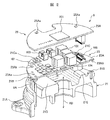
- FIG. 2 is an exploded perspective view including a cross section of the electronic control device 9 of the electric power steering device 1 according to the embodiment of the present invention.
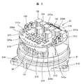
- FIG. 3 is a perspective view of the electronic control unit 9 excluding the control board 23 from FIG. In FIG. 2, the cover covering the power supply board 23 and the control board 25 is not shown.
- the electronic control unit 9 is fixed to one end (the end opposite to the output shaft side) of the electric motor along the axial direction AD of the rotating shaft (output shaft).
- the axial direction AD is defined with reference to the rotating shaft (output shaft) of the electric motor, and in the following description, the direction of the rotating shaft along the axial direction AD will be simply referred to as the axial direction.
- the electronic control device 9 includes a base (basic substance) 21, a power supply board 23 fixed to the base 21, and a control board 25.
- the base 21 is fixed to the motor housing (not shown) of the electric motor unit 8.
- the base 21 and the motor housing are manufactured by using an aluminum alloy or the like.
- the power supply board 23 and the control board 25 are laminated in the axial direction AD, and the power supply board 23 is arranged on the base 21 side (lower side) with respect to the control board 25. That is, the control board 25 is arranged on the side (upper side) opposite to the base 21 side with respect to the power supply board 23.
- the lead wire (coil input terminal) 8A of the coil of the electric motor provided in the electric motor unit 8 penetrates the base 21 and is pulled out to the upper surface side (opposite side of the base 21 side) of the power supply board 23 to lead out to the power supply board. It is electrically connected to the output terminal of the switching element 101 of 23.
- the substrate member (power supply board member) 23A of the power supply board 23 is provided with a through hole 23Aa, and the coil input terminal 8A is pulled out to the upper surface side of the power supply board 23 through the through hole 23Aa.
- the coil input terminal 8A is soldered to the substrate member 23A and electrically connected to the power supply substrate 23.
- the method is not limited to solder, and may be fusing (heat caulking), TIG welding, press fitting, or the like.
- the coil lead wire (coil input terminal) 8A described above is treated as a part of the coil, and will be simply referred to as a coil.
- a switching element 101, a capacitor 102, a power supply terminal 103, a magnetic sensor 104, an inter-board connector 105, an FS relay / power choke coil 106 (see FIG. 5), and the like are arranged on the power supply board 23, and these electrical and electronic components are used as a power source. It constitutes a circuit (power conversion circuit).
- the switching element 101 converts a DC power supply into a three-phase AC power supply.
- the capacitor 102 is composed of an aluminum electrolytic capacitor or the like, and suppresses voltage fluctuations such as switching noise by performing charging and discharging.
- the power supply terminal 103 is a terminal to which an external power supply is connected.
- the magnetic sensor 104 is a sensor that detects the rotation angle of the electric motor.
- the inter-board connector 105 is a circuit component that makes an electrical connection with the control board 25.
- the FS relay / power choke coil 106 the FS relay is a circuit component that cuts off the current flowing through the electric motor in the event of a failure, and the power choke coil is a circuit component that suppresses the propagation of switching noise.
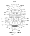
- FIG. 4 is a plan view showing a switching element mounting surface of the power supply board 23.
- the first system and the second system are separately arranged on the left and right sides of the straight line L23 with the straight line L23 passing through the axis center position O and parallel to the component mounting surface of the substrate 23 as a boundary.
- the left side of the straight line L23 is referred to as the first system, and the right side is referred to as the second system.
- the power supply board member 23A of the power supply board (inverter board, power conversion board) 23 has a plurality of holes (through holes, coil lead wire insertion holes) through which the coil lead wire 8A of the first system (on the power supply side) is inserted.
- Insertion hole It has a second insertion hole portion R2A having 23Aa-2U, 23Aa-2V, 23Aa-2W.
- a control board 25 is provided on the upper side of the power supply board 23 (the side opposite to the base 21 side), and the power supply board 23 and the control board 25 are electrically connected by inter-board connectors 105 and 202.
- the power supply board 23 is provided with the inter-board connector 105
- the control board 25 is provided with the inter-board connector 202.
- the control board 25 is provided with an integrated circuit 201 or the like for calculating a control signal for controlling the electric motor.
- the first insertion hole portion R1A and the second insertion hole portion R2A are arranged together on the same side of the power supply board 23 with respect to the axis center position O in the direction along the straight line L23. That is, the first insertion hole portion R1A and the second insertion hole portion R2A are arranged so as to be aggregated on the same side with respect to the axis center position O in the direction along the straight line L23. In this case, the first insertion hole portion R1A and the second insertion hole portion R2A are arranged on the outer peripheral edge portion of the power supply board 23, and the first holes 23Aa-2U, 23Aa-2V, 23Aa-2W and the second of the first system are arranged.
- the six holes consisting of the second holes 23Aa-2U, 23Aa-2V, and 23Aa-2W of the system are arranged at equal intervals.
- the six holes are arranged in an arc shape, but they may be arranged in a straight line.
- the first coil lead wire 8A-1U, 8A-1V, 8A-1W (see FIG. 7), the first switching element 101-1, the first capacitor 102-1, and the first power supply terminal 103 -1 is mounted, and the first insertion hole portion R1A to which the first coil lead wire 8A-1U, 8A-1V, 8A-1W is connected, and the first switching element 101-1 to which the first switching element 101-1 is arranged are arranged.
- the mounting unit R1B, the first capacitor mounting unit R1C in which the first capacitor 102-1 is arranged, and the first power supply terminal mounting unit R1D in which the first power supply terminal 103-1 is arranged are L1 having an L-shaped straight line.
- the terminal mounting portions R1D are arranged in this order.
- the second coil lead wire 8A-2U, 8A-2V, 8A-2W (see FIG. 7), the second switching element 101-2, the second capacitor 102-2, and the second power supply terminal
- the second switching in which 103-2 is mounted, the second insertion hole R2A to which the second coil lead wires 8A-2U, 8A-2V, and 8A-2W are connected, and the second switching element 101-2 are arranged.
- the element mounting portion R2B, the second capacitor mounting portion R2C in which the second capacitor 102-2 is arranged, and the second power supply terminal mounting portion R2D in which the second power supply terminal 103-2 is arranged are L-shaped straight line segments.
- the second insertion hole portion R2A side toward the second power supply terminal mounting portion R2D side the second insertion hole portion R2A, the second switching element mounting portion R2B, the second capacitor mounting portion R2C, and the second The power supply terminal mounting portions R2D are arranged in this order.
- the mounting unit R2B, the second capacitor mounting unit R2C, and the second power supply terminal mounting unit R2D are arranged line-symmetrically with respect to the straight line L23.
- the magnetic sensor 104 is arranged at the axis center position O.
- the inter-board connector 105 is arranged on the opposite side of the first insertion hole portion R1A and the second insertion hole portion R2A with the shaft center position O interposed therebetween. Therefore, the magnetic sensor 104 is arranged between the first insertion hole portion R1A and the second insertion hole portion R2A and the inter-board connector mounting portion R3.
- the assembly equipment can be made smaller.
- the mounting efficiency can be improved and the board size can be reduced by improving the wiring efficiency.
- the switching element The arrangement of 101 and the capacitor 102 can be optimized, and the product size can be reduced.
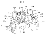
- FIG. 5 is a perspective view including a cross section showing a state in which the power supply board 23 is assembled to the base 21.
- the first coil lead wire 8A-1U, 8A-1V, 8A-1W and the first switching element 101-1 are arranged at close positions
- the second coil lead wire 8A- It is preferable that the 2U, 8A-2V, 8A-2W and the second switching element 101-2 are arranged at close positions.
- the base 21 is provided with a convex portion 21D protruding toward the power supply board 23 side, and the upper end surface of the convex portion 21D is brought into contact with the back surface of the power supply board 23. ..
- no component can be mounted on the back surface side of the first switching element mounting portion R1B and the second switching element mounting portion R2B on the power supply board 23.
- the first coil lead wires 8A-1U, 8A-1V, 8A-1W and the second coil lead wires 8A-2U, 8A-2V, 8A-2W are arranged together in the same row.
- the 1 switching element 101-1 and the 2nd switching element 101-2 are centrally arranged. That is, the first switching element 101-1 and the second switching element 101-2 are collectively mounted on the upper surface of the power supply board 23.
- the first switching element mounting portion R1B and the second switching element mounting portion R2B are arranged apart from each other, the range of the convex portion 21D becomes large and the component mounting surface on the back surface side of the power supply board 23 becomes small.
- the convex portion 21D with which the back surface side of the first switching element mounting portion R1B and the second switching element mounting portion R2B of the power supply board 23 abut can be compactly combined, and the space lost by the convex portion 21D can be reduced. Can be done. Further, when the first switching element mounting portion R1B and the second switching element mounting portion R2B are arranged apart from each other, if the convex portion 21D is divided, the component mounting surface on the back surface side of the power supply board 23 is divided, and the component mounting surface is divided. Mounting efficiency is reduced. In this embodiment, it is possible to prevent the component mounting surface from being divided. As a result, in this embodiment, the mounting efficiency of the components on the back surface side of the power supply board 23 is improved.
- high heat generation components such as the switching element 101 are mounted on the upper surface of the power supply board 23, and low heat generation components such as the FS relay / power choke coil 106 are mounted on the lower surface of the power supply board 23, and only the components that require cooling are mounted.
- the board mounting efficiency can be improved.
- the substrate (housing) 21 and the power supply board 23 can be brought into contact with each other, and the cooling effect can be improved.
- the switching element (MOSFET) 101 By integrating the switching element (MOSFET) 101, the cooling portion of the aluminum housing structure constituting the substrate (housing) 21 can be simplified, which makes it possible to reduce the product size.
- the base 21 is fixed to a motor housing (not shown) with a bolt (not shown). For this reason, a plurality of bolt insertion holes 21A through which bolts are inserted are provided on the outer periphery of the base 21 on the motor housing side.
- the substrate 21 is also a member that also serves as a heat sink that dissipates heat generated by the switching element 101 and the like of the power supply substrate 23.
- the substrate 21 is provided with a convex portion 21D. That is, the substrate 21 has a first convex portion 21D that comes into contact with a portion of the back surface of the power supply substrate 23 that is located directly below the mounting portion on which the high heat generating component including the switching element 101 is mounted.
- the substrate 21 is provided with a plurality of power supply board fixing portions 21B for fixing the power supply board 23 next to the convex portion 21D (see FIG. 3).
- a screw (not shown) is inserted into the through hole 23Ab of the power supply board 23, and the power supply board 23 is screwed to the power supply board fixing portion 21B.
- a screw (not shown) is inserted into the through hole 25Aa of the control board 25, and the control board 25 is screwed to the fixing portion (control board fixing portion) 21Ca provided on the base 21. Since the control board 25 is separated and stacked on the upper side of the power supply board 23, the control board fixing portion 21Ca is located higher than the power supply board fixing portion 21B and is higher than the upper end surface of the convex portion 21D. It is provided on the upper end surface of the stretched columnar portion 21C.
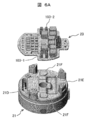
- FIG. 6A is a perspective view showing a deflection prevention structure of the power supply board.
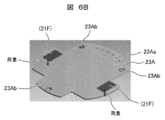
- FIG. 6B is a perspective view of a power supply board showing the arrangement of the deflection prevention structure and the load input position in the analysis of the amount of deflection.
- FIG. 6C is a perspective view of a power supply board showing an analysis result of the amount of deflection when the deflection prevention structure is provided.
- FIG. 6D is a perspective view of a power supply board showing an analysis result of the amount of deflection when there is no anti-deflection structure.
- the electronic components and the power supply terminal 103 are symmetrically arranged on the mounting surface in the direction perpendicular to the straight line L23 from the axis center position O of the power supply board 23, and the first power supply terminal mounting portion R1D and the first power supply terminal mounting portion R1D on the power supply board 23 are arranged symmetrically.
- the back surface side of the power supply terminal mounting portion R2D is in contact with the substrate (housing) 21. That is, the first power supply terminal 101-1 and the first power supply terminal 101-1 are on the mounting surface in the direction parallel to the substrate surface, orthogonal to the straight line L23 passing through the axis center position O of the power supply board 23 and parallel to the substrate surface of the power supply board 23.
- the two power supply terminals 101-2 are arranged symmetrically with respect to the straight line L23, and the back surface side of the first power supply terminal mounting portion R1D and the second power supply terminal mounting portion R1D in the power supply board 23 is the base 21 supporting the power supply board 23. I'm in contact.
- the base 21 is provided with a convex portion 21F that contacts the back surface side of the first power supply terminal mounting portion R1D and the second power supply terminal mounting portion R2D on the power supply board 23.
- the substrate 21 has a second convex portion 21F and a first power supply terminal (1st power supply terminal) in contact with a portion of the back surface of the power supply board 23 located directly below the mounting portion on which the first power supply terminal (power supply terminal of the first system) is mounted. It has a third convex portion 21F that comes into contact with a portion located directly below the mounting portion on which the power supply terminal of the second system) is mounted.
- the terminal on the external power supply side is inserted into the power supply terminal 103 with a strong force from above to below.
- the power supply board 23 is distorted by receiving this strong force via the power supply terminal 103.
- the amount of strain of the power supply board 23 is suppressed when the external power supply terminals are joined, as compared with the structure without the convex portion 21F of FIG. 6D.
- a substrate deflection prevention structure (convex portion 21F) can be provided on the outer peripheral portion of the power supply substrate 23, and the power supply substrate 23 can be provided. Deflection (strain) can be reduced. As a result, it is possible to eliminate the need for screw fixing in the vicinity of the power supply terminal 103, and the mounting efficiency of the power supply board 23 is improved.
- the power supply board 23 since the magnetic sensor (rotation angle sensor) 104 is mounted at the axis center position O, the board deflection prevention structure cannot be provided.
- the convex portion 21E that contacts the back surface is also provided on the back surface side of the inter-board connector mounting portion R3 in which the inter-board connector 105 is arranged. That is, the substrate 21 has a fourth convex portion that comes into contact with a portion of the back surface of the power supply substrate 23 that is located directly below the mounting portion on which the inter-board connector 105 is mounted.
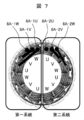
- FIG. 7 is a conceptual diagram illustrating end treatment of the coil wire.
- FIG. 8 is a diagram showing a comb tooth jig used for end treatment of a coil wire.
- the following assembly method can be implemented as the assembly method of the electronic control unit.
- a control board 25 provided on the upper part of the power supply board 23 and An inter-board connector 105 for electrically connecting the power supply board 23 and the control board 25 is provided.
- the first insertion hole portion R1A and the second insertion hole portion R2A are methods for assembling the electronic control device 9 which are collectively arranged on the same side of the power supply board 23.
- Two coil wires 8A-1U, 8A-1V, 8A-1W, 8A-2U, 8A-2V, 8A-2W are wired together for each system, and coil wires 8A-1U, 8A-1V, 8A-1W.
- 8A-2U, 8A-2V, 8A-2W are corrected inside the electric motor so that the ends are linear in the same row, and a plurality of holes 23Aa-2U, 23Aa-2V, 23Aa-2W of the first insertion hole R1A are formed. And, it is assembled by inserting it into a plurality of holes 23Aa-2U, 23Aa-2V, 23Aa-2W of the second insertion hole portion R2A.
- the present invention is not limited to the above-described examples, and includes various modifications.
- the above-described embodiment has been described in detail in order to explain the present invention in an easy-to-understand manner, and is not necessarily limited to those having all the configurations.
Landscapes
- Engineering & Computer Science (AREA)
- Microelectronics & Electronic Packaging (AREA)
- Power Engineering (AREA)
- Manufacturing & Machinery (AREA)
- Chemical & Material Sciences (AREA)
- Combustion & Propulsion (AREA)
- Transportation (AREA)
- Mechanical Engineering (AREA)
- Power Steering Mechanism (AREA)
- Mounting Of Printed Circuit Boards And The Like (AREA)
- Inverter Devices (AREA)
Abstract
Description
第1系統のコイル線が挿通される複数の孔を有する第1挿通孔部と、
第2系統のコイル線が挿通される複数の孔を有する第2挿通孔部と、を有する電源基板と、
前記電源基板の上部に設けられる制御基板と、
前記電源基板と前記制御基板とを電気的に接続する基板間コネクタと、を備え、
前記第1挿通孔部と前記第2挿通孔部とは、前記電源基板の同一側にまとめて配置されている。
なお、半田に限定されるものではなく、ヒュージング(熱かしめ)、TIG溶接、プレスフィット等でもよい。
また、スイッチング素子101の裏側には電子部品を搭載しないことで、基体(筐体)21と電源基板23とを接触させることができ、冷却効果を向上することができる。スイッチング素子(MOSFET)101の集約化によって、基体(筐体)21を構成するアルミハウジング構造の冷却部を簡易化することができ、これにより製品サイズの低減が可能になる。
図6Dは、たわみ防止構造が無い場合のたわみ量の解析結果を示す電源基板の斜視図である。
第2系統のコイル線8A-2U,8A-2V,8A-2Wが挿通される複数の孔23Aa-2U,23Aa-2V,23Aa-2Wを有する第2挿通孔部R2Aと、を有する電源基板23と、
電源基板23の上部に設けられる制御基板25と、
電源基板23と制御基板25とを電気的に接続する基板間コネクタ105と、を備え、
第1挿通孔部R1Aと第2挿通孔部R2Aとは、電源基板23の同一側にまとめて配置されている電子制御装置9の組立方法であって、
二系統のコイル線8A-1U,8A-1V,8A-1W,8A-2U,8A-2V,8A-2Wを系統毎に纏めて配線し、コイル線8A-1U,8A-1V,8A-1W,8A-2U,8A-2V,8A-2Wの終端が同列直線状になるように電動モータ内部で矯正し、第1挿通孔部R1Aの複数の孔23Aa-2U,23Aa-2V,23Aa-2W及び第2挿通孔部R2Aの複数の孔23Aa-2U,23Aa-2V,23Aa-2Wに挿通して組み立てる。
例えば、上記した実施例は本発明を分かりやすく説明するために詳細に説明したものであり、必ずしも全ての構成を備えるものに限定されるものではない。また、実施例の構成の一部を他の構成に置き換えることが可能であり、実施例の構成の一部について、他の構成を追加することが可能である。
Claims (10)
- 第1系統のコイル線が挿通される複数の孔を有する第1挿通孔部と、第2系統のコイル線が挿通される複数の孔を有する第2挿通孔部と、を有する電源基板と、
前記電源基板の上部に設けられ、前記電源基板と電気的に接続される制御基板と、
前記電源基板と前記制御基板が固定される金属製の基体と、を備え、
前記第1挿通孔部と前記第2挿通孔部とは、前記電源基板の同一側にまとめて配置されている電子制御装置。 - 請求項1に記載の電子制御装置において、
前記電源基板は、前記制御基板と電気的に接続するための基板間コネクタを備え、
前記基板間コネクタは、前記第1挿通孔部及び前記第2挿通孔部に対して前記制御基板の中心を挟んで反対側に設けられている電子制御装置。 - 請求項2に記載の電子制御装置において、
第1系統のスイッチング素子、第2系統のスイッチング素子、第1系統のコンデンサ、第2系統のコンデンサ、第1系統の電源端子、及び第2系統の電源端子を備え、
前記第1系統のコイル線、前記第1系統のスイッチング素子、前記第1系統のコンデンサ、及び前記第1系統の電源端子は、この順番で前記電源基板に実装され、
前記第2系統のコイル線、前記第2系統のスイッチング素子、前記第2系統のコンデンサ、及び前記第2系統の電源端子は、この順番で前記電源基板に実装されている電子制御装置。 - 請求項3に記載の電子制御装置において、
FSリレー及びパワーチョークコイルを備え、
前記スイッチング素子を含む高発熱部品を前記電源基板の上面側に配置し、前記FSリレー及び前記パワーチョークコイルなどの低発熱部品を前記電源基板の下面側に配置した電子制御装置。 - 請求項3又は4に記載の電子制御装置において、
前記基体は、前記電源基板の裏面のうち前記スイッチング素子を含む高発熱部品が実装される実装部の直下に位置する部分と接触する第1凸部を有する電子制御装置。 - 請求項3乃至5のいずれかに記載の電子制御装置において、
前記電源基板の軸中心位置を通り前記電源基板の基板面に平行な直線に対して直交し前記基板面に平行な方向の実装面上に、前記第1系統の電源端子と前記第2系統の電源端子とを前記直線に対して対称配置し、前記電源基板における前記第1系統の電源端子の実装面及び第2系統の電源端子の実装面の裏面側を、前記電源基板を支持する基体と接触させている電子制御装置。 - 請求項3乃至6のいずれかに記載の電子制御装置において、
前記基体は、前記電源基板の裏面のうち前記第1系統の電源端子が実装される実装部の直下に位置する部分に接触する第2凸部と前記第2系統の電源端子が実装される実装部の直下に位置する部分と接触する第3凸部とを有する電子制御装置。 - 請求項2乃至7のいずれかに記載の電子制御装置において、
前記基体は、前記電源基板の裏面のうち前記基板間コネクタが実装される実装部の直下に位置する部分と接触する第4凸部を有する電子制御装置。 - 請求項2乃至8のいずれかに記載の電子制御装置において、
前記第1挿通孔部及び前記第2挿通孔部と前記基板間コネクタの実装部との間に実装された磁気センサを備える電子制御装置。 - 第1系統のコイル線が挿通される複数の孔を有する第1挿通孔部と、
第2系統のコイル線が挿通される複数の孔を有する第2挿通孔部と、を有する電源基板と、
前記電源基板の上部に設けられる制御基板と、
前記電源基板と前記制御基板とを電気的に接続する基板間コネクタと、を備え、
前記第1挿通孔部と前記第2挿通孔部とは、前記電源基板の同一側にまとめて配置されている電子制御装置の組立方法であって、
二系統の前記コイル線を系統毎に纏めて配線し、前記コイル線の終端が同列直線状になるように電動モータ内部で矯正し、前記第1挿通孔部の前記複数の孔及び前記第2挿通孔部の前記複数の孔に挿通して組み立てる電子制御装置の組立方法。
Priority Applications (4)
| Application Number | Priority Date | Filing Date | Title |
|---|---|---|---|
| DE112019006832.6T DE112019006832T5 (de) | 2019-03-19 | 2019-12-24 | Elektronische Steuereinheit und Verfahren zum Montieren der elektronischen Steuereinheit |
| JP2021506174A JP7089635B2 (ja) | 2019-03-19 | 2019-12-24 | 電動駆動装置 |
| US17/435,961 US11956900B2 (en) | 2019-03-19 | 2019-12-24 | Electronic control unit and method for assembling electronic control unit |
| CN201980087807.4A CN113544963B (zh) | 2019-03-19 | 2019-12-24 | 电子控制装置及电子控制装置的组装方法 |
Applications Claiming Priority (2)
| Application Number | Priority Date | Filing Date | Title |
|---|---|---|---|
| JP2019-050819 | 2019-03-19 | ||
| JP2019050819 | 2019-03-19 |
Publications (1)
| Publication Number | Publication Date |
|---|---|
| WO2020188934A1 true WO2020188934A1 (ja) | 2020-09-24 |
Family
ID=72519817
Family Applications (1)
| Application Number | Title | Priority Date | Filing Date |
|---|---|---|---|
| PCT/JP2019/050495 Ceased WO2020188934A1 (ja) | 2019-03-19 | 2019-12-24 | 電子制御装置及び電子制御装置の組立方法 |
Country Status (5)
| Country | Link |
|---|---|
| US (1) | US11956900B2 (ja) |
| JP (1) | JP7089635B2 (ja) |
| CN (1) | CN113544963B (ja) |
| DE (1) | DE112019006832T5 (ja) |
| WO (1) | WO2020188934A1 (ja) |
Cited By (6)
| Publication number | Priority date | Publication date | Assignee | Title |
|---|---|---|---|---|
| US20220271613A1 (en) * | 2021-02-19 | 2022-08-25 | Jtekt Corporation | Motor control device |
| EP4096073A4 (en) * | 2021-02-10 | 2023-11-15 | NSK Ltd. | ELECTRICAL DRIVE DEVICE, ELECTRIC POWER STEERING DEVICE AND PRODUCTION METHOD FOR AN ELECTRONIC CONTROL DEVICE |
| WO2024142213A1 (ja) * | 2022-12-27 | 2024-07-04 | 三菱電機株式会社 | 電子制御装置および電動パワーステアリング装置 |
| US12142972B2 (en) | 2021-02-10 | 2024-11-12 | Nsk Ltd. | Electric driving device and electric power steering device |
| US12512731B2 (en) | 2021-02-10 | 2025-12-30 | Nsk Ltd. | Electric driving device and electric power steering device |
| EP4641894A4 (en) * | 2022-12-21 | 2025-12-31 | Jtekt Corp | ENGINE DEVICE |
Families Citing this family (1)
| Publication number | Priority date | Publication date | Assignee | Title |
|---|---|---|---|---|
| CN116494173A (zh) * | 2023-05-23 | 2023-07-28 | 上海宏晴智能科技有限公司 | 电批及其控制构件和层置线路板组件 |
Citations (4)
| Publication number | Priority date | Publication date | Assignee | Title |
|---|---|---|---|---|
| JP2015193371A (ja) * | 2014-03-27 | 2015-11-05 | 日本電産エレシス株式会社 | 電動パワーステアリング用電子制御装置 |
| WO2016002687A1 (ja) * | 2014-06-30 | 2016-01-07 | 日本精工株式会社 | モータ並びにそれを搭載した電動パワーステアリング装置及び車両 |
| JP2016036244A (ja) * | 2014-07-31 | 2016-03-17 | 株式会社デンソー | 駆動装置、および、これを用いた電動パワーステアリング装置 |
| WO2017068636A1 (ja) * | 2015-10-20 | 2017-04-27 | 三菱電機株式会社 | 一体型電動パワーステアリング装置、及びその製造方法 |
Family Cites Families (10)
| Publication number | Priority date | Publication date | Assignee | Title |
|---|---|---|---|---|
| JP2013103535A (ja) * | 2011-11-10 | 2013-05-30 | Honda Elesys Co Ltd | 電動パワーステアリング用電子制御ユニット |
| JP5561301B2 (ja) * | 2012-03-29 | 2014-07-30 | 株式会社デンソー | 駆動装置およびその製造方法 |
| JP6184531B2 (ja) * | 2014-02-14 | 2017-08-23 | 三菱電機株式会社 | 制御装置付き回転電機および電動パワーステアリング装置 |
| JP6123848B2 (ja) * | 2014-07-31 | 2017-05-10 | 株式会社デンソー | 駆動装置、および、これを用いた電動パワーステアリング装置 |
| JP6852573B2 (ja) * | 2017-06-01 | 2021-03-31 | 日本精工株式会社 | 電動駆動装置及び電動パワーステアリング装置 |
| JP6922435B2 (ja) * | 2017-06-01 | 2021-08-18 | 日本精工株式会社 | 電動駆動装置、及び電動パワーステアリング装置 |
| JP6798427B2 (ja) * | 2017-06-01 | 2020-12-09 | 日本精工株式会社 | 電動駆動装置、及び電動パワーステアリング装置 |
| CN111033978B (zh) * | 2017-09-28 | 2022-11-29 | 日本电产株式会社 | 马达和电动助力转向装置 |
| JP6940358B2 (ja) * | 2017-09-29 | 2021-09-29 | 日本電産エレシス株式会社 | 回路基板、モータ駆動装置および電動パワーステアリング装置 |
| JP7222175B2 (ja) * | 2017-11-09 | 2023-02-15 | 株式会社ジェイテクト | モータ装置 |
-
2019
- 2019-12-24 US US17/435,961 patent/US11956900B2/en active Active
- 2019-12-24 CN CN201980087807.4A patent/CN113544963B/zh active Active
- 2019-12-24 DE DE112019006832.6T patent/DE112019006832T5/de active Pending
- 2019-12-24 WO PCT/JP2019/050495 patent/WO2020188934A1/ja not_active Ceased
- 2019-12-24 JP JP2021506174A patent/JP7089635B2/ja active Active
Patent Citations (4)
| Publication number | Priority date | Publication date | Assignee | Title |
|---|---|---|---|---|
| JP2015193371A (ja) * | 2014-03-27 | 2015-11-05 | 日本電産エレシス株式会社 | 電動パワーステアリング用電子制御装置 |
| WO2016002687A1 (ja) * | 2014-06-30 | 2016-01-07 | 日本精工株式会社 | モータ並びにそれを搭載した電動パワーステアリング装置及び車両 |
| JP2016036244A (ja) * | 2014-07-31 | 2016-03-17 | 株式会社デンソー | 駆動装置、および、これを用いた電動パワーステアリング装置 |
| WO2017068636A1 (ja) * | 2015-10-20 | 2017-04-27 | 三菱電機株式会社 | 一体型電動パワーステアリング装置、及びその製造方法 |
Cited By (11)
| Publication number | Priority date | Publication date | Assignee | Title |
|---|---|---|---|---|
| EP4096073A4 (en) * | 2021-02-10 | 2023-11-15 | NSK Ltd. | ELECTRICAL DRIVE DEVICE, ELECTRIC POWER STEERING DEVICE AND PRODUCTION METHOD FOR AN ELECTRONIC CONTROL DEVICE |
| US11909274B2 (en) | 2021-02-10 | 2024-02-20 | Nsk Ltd. | Electric driving device, electric power steering device, and method for manufacturing electronic control unit |
| US12142972B2 (en) | 2021-02-10 | 2024-11-12 | Nsk Ltd. | Electric driving device and electric power steering device |
| US12512731B2 (en) | 2021-02-10 | 2025-12-30 | Nsk Ltd. | Electric driving device and electric power steering device |
| US20220271613A1 (en) * | 2021-02-19 | 2022-08-25 | Jtekt Corporation | Motor control device |
| CN114977672A (zh) * | 2021-02-19 | 2022-08-30 | 株式会社捷太格特 | 马达控制装置 |
| US12095337B2 (en) * | 2021-02-19 | 2024-09-17 | Jtekt Corporation | Motor control device with layout to decrease difference in current paths |
| EP4641894A4 (en) * | 2022-12-21 | 2025-12-31 | Jtekt Corp | ENGINE DEVICE |
| WO2024142213A1 (ja) * | 2022-12-27 | 2024-07-04 | 三菱電機株式会社 | 電子制御装置および電動パワーステアリング装置 |
| JPWO2024142213A1 (ja) * | 2022-12-27 | 2024-07-04 | ||
| JP7789233B2 (ja) | 2022-12-27 | 2025-12-19 | 三菱電機モビリティ株式会社 | 電子制御装置および電動パワーステアリング装置 |
Also Published As
| Publication number | Publication date |
|---|---|
| JP7089635B2 (ja) | 2022-06-22 |
| DE112019006832T5 (de) | 2021-12-02 |
| JPWO2020188934A1 (ja) | 2021-12-02 |
| CN113544963B (zh) | 2025-08-08 |
| CN113544963A (zh) | 2021-10-22 |
| US11956900B2 (en) | 2024-04-09 |
| US20220159838A1 (en) | 2022-05-19 |
Similar Documents
| Publication | Publication Date | Title |
|---|---|---|
| JP7089635B2 (ja) | 電動駆動装置 | |
| JP6680054B2 (ja) | 駆動装置、および、これを用いた電動パワーステアリング装置 | |
| CN108137084B (zh) | 一体型电动助力转向装置及其制造方法 | |
| JP6138358B2 (ja) | 電動パワーステアリング装置 | |
| JP4285435B2 (ja) | 電力変換装置 | |
| JP6443055B2 (ja) | 駆動装置、および、駆動装置の製造方法 | |
| JP7096886B2 (ja) | 電動パワーステアリング装置の電動駆動装置 | |
| JP6161816B2 (ja) | 一体型電動パワーステアリング装置、及びその製造方法 | |
| CN111971880B (zh) | 电动助力转向装置 | |
| CN107529347A (zh) | 电动助力转向装置 | |
| JP5466679B2 (ja) | 電動アクチュエータの電子回路装置 | |
| JP7291572B2 (ja) | 電動駆動装置及び電動駆動装置の組立方法 | |
| JP2020188556A (ja) | モータ | |
| JP7068449B2 (ja) | 通電端子組立体及び電動駆動装置 | |
| US20210408866A1 (en) | Electric driving device | |
| JP7321361B2 (ja) | 回転電機装置および電動パワーステアリング装置 | |
| JP7102548B2 (ja) | 電子制御装置及び電動パワーステアリング装置 | |
| JP2018207639A (ja) | 電動駆動装置、及び電動パワーステアリング装置 | |
| JP4952666B2 (ja) | 電動式パワーステアリング装置 | |
| JP2008290675A (ja) | 電動パワーステアリング装置 | |
| JP2014161174A (ja) | モータ装置 | |
| CN103368349B (zh) | 车用交流发电机 | |
| CN120937222A (zh) | 旋转电机装置及电动助力转向装置 |
Legal Events
| Date | Code | Title | Description |
|---|---|---|---|
| 121 | Ep: the epo has been informed by wipo that ep was designated in this application |
Ref document number: 19919648 Country of ref document: EP Kind code of ref document: A1 |
|
| ENP | Entry into the national phase |
Ref document number: 2021506174 Country of ref document: JP Kind code of ref document: A |
|
| 122 | Ep: pct application non-entry in european phase |
Ref document number: 19919648 Country of ref document: EP Kind code of ref document: A1 |
|
| WWG | Wipo information: grant in national office |
Ref document number: 201980087807.4 Country of ref document: CN |