WO2020188922A1 - 光回路基板 - Google Patents
光回路基板 Download PDFInfo
- Publication number
- WO2020188922A1 WO2020188922A1 PCT/JP2019/049295 JP2019049295W WO2020188922A1 WO 2020188922 A1 WO2020188922 A1 WO 2020188922A1 JP 2019049295 W JP2019049295 W JP 2019049295W WO 2020188922 A1 WO2020188922 A1 WO 2020188922A1
- Authority
- WO
- WIPO (PCT)
- Prior art keywords
- layer
- conductor
- recess
- circuit board
- optical waveguide
- Prior art date
- Legal status (The legal status is an assumption and is not a legal conclusion. Google has not performed a legal analysis and makes no representation as to the accuracy of the status listed.)
- Ceased
Links
Images

Classifications
-
- G—PHYSICS
- G02—OPTICS
- G02B—OPTICAL ELEMENTS, SYSTEMS OR APPARATUS
- G02B6/00—Light guides; Structural details of arrangements comprising light guides and other optical elements, e.g. couplings
- G02B6/10—Light guides; Structural details of arrangements comprising light guides and other optical elements, e.g. couplings of the optical waveguide type
- G02B6/12—Light guides; Structural details of arrangements comprising light guides and other optical elements, e.g. couplings of the optical waveguide type of the integrated circuit kind
- G02B6/122—Basic optical elements, e.g. light-guiding paths
-
- G—PHYSICS
- G02—OPTICS
- G02B—OPTICAL ELEMENTS, SYSTEMS OR APPARATUS
- G02B6/00—Light guides; Structural details of arrangements comprising light guides and other optical elements, e.g. couplings
- G02B6/24—Coupling light guides
- G02B6/42—Coupling light guides with opto-electronic elements
- G02B6/4201—Packages, e.g. shape, construction, internal or external details
- G02B6/4204—Packages, e.g. shape, construction, internal or external details the coupling comprising intermediate optical elements, e.g. lenses, holograms
- G02B6/4214—Packages, e.g. shape, construction, internal or external details the coupling comprising intermediate optical elements, e.g. lenses, holograms the intermediate optical element having redirecting reflective means, e.g. mirrors, prisms for deflecting the radiation from horizontal to down- or upward direction toward a device
-
- H—ELECTRICITY
- H05—ELECTRIC TECHNIQUES NOT OTHERWISE PROVIDED FOR
- H05K—PRINTED CIRCUITS; CASINGS OR CONSTRUCTIONAL DETAILS OF ELECTRIC APPARATUS; MANUFACTURE OF ASSEMBLAGES OF ELECTRICAL COMPONENTS
- H05K1/00—Printed circuits
- H05K1/02—Details
- H05K1/11—Printed elements for providing electric connections to or between printed circuits
-
- G—PHYSICS
- G02—OPTICS
- G02B—OPTICAL ELEMENTS, SYSTEMS OR APPARATUS
- G02B6/00—Light guides; Structural details of arrangements comprising light guides and other optical elements, e.g. couplings
- G02B6/10—Light guides; Structural details of arrangements comprising light guides and other optical elements, e.g. couplings of the optical waveguide type
- G02B6/12—Light guides; Structural details of arrangements comprising light guides and other optical elements, e.g. couplings of the optical waveguide type of the integrated circuit kind
- G02B2006/12083—Constructional arrangements
- G02B2006/12104—Mirror; Reflectors or the like
-
- H—ELECTRICITY
- H05—ELECTRIC TECHNIQUES NOT OTHERWISE PROVIDED FOR
- H05K—PRINTED CIRCUITS; CASINGS OR CONSTRUCTIONAL DETAILS OF ELECTRIC APPARATUS; MANUFACTURE OF ASSEMBLAGES OF ELECTRICAL COMPONENTS
- H05K1/00—Printed circuits
- H05K1/02—Details
- H05K1/0274—Optical details, e.g. printed circuits comprising integral optical means
-
- H—ELECTRICITY
- H05—ELECTRIC TECHNIQUES NOT OTHERWISE PROVIDED FOR
- H05K—PRINTED CIRCUITS; CASINGS OR CONSTRUCTIONAL DETAILS OF ELECTRIC APPARATUS; MANUFACTURE OF ASSEMBLAGES OF ELECTRICAL COMPONENTS
- H05K2201/00—Indexing scheme relating to printed circuits covered by H05K1/00
- H05K2201/20—Details of printed circuits not provided for in H05K2201/01 - H05K2201/10
- H05K2201/2054—Light-reflecting surface, e.g. conductors, substrates, coatings, dielectrics
Definitions
- This disclosure relates to an optical circuit board.
- optical communication networks capable of communicating large volumes of data at high speed have expanded, and there are various optical communication devices using such optical communication networks.
- Such an apparatus is equipped with an optical circuit board connected to the substrate by an optical waveguide, for example, as described in Patent Document 1.
- the optical circuit board includes a wiring board and an optical waveguide.
- the optical waveguide includes a core layer, a clad layer formed on both main surfaces of the core layer, and a reflection mirror portion penetrating the clad layer and the core layer, and is wired via a conductor layer located on the surface of a wiring board. It is provided on the board.
- the reflection mirror portion has a recess in at least a part of the clad layer on the conductor layer side.
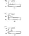
- FIG. (A) to (C) are schematic views showing various shapes of the recesses formed in the reflection mirror portion.
- the optical waveguide may be connected on the conductor layer formed on the surface of the wiring board.
- the conductor layer formed on the wiring board and the clad layer formed on the optical waveguide come into contact with each other.
- the conductor layer is made of a metal having a small thermal expansion coefficient
- the clad layer is made of a resin or the like having a larger thermal expansion coefficient than the metal. Therefore, due to the difference in thermal expansion and contraction, the conductor layer and the clad layer are easily separated from each other. As a result, the stability and reliability of the optical circuit board are reduced.
- the reflection mirror portion when the optical waveguide is viewed in cross section in the thickness direction, the reflection mirror portion has a recess in at least a part of the clad layer on the conductor layer side. Therefore, even if the difference in thermal expansion and contraction between the conductor layer and the clad layer is relatively large, the stress generated at the boundary between the conductor layer and the clad layer is easily dispersed by the recesses. As a result, the conductor layer and the clad layer are less likely to be separated from each other, and the stability and reliability of the optical circuit board can be improved.
- the optical circuit board according to the embodiment of the present disclosure will be described with reference to FIGS. 1 and 2.
- the optical circuit board 1 according to the embodiment shown in FIG. 1 includes a wiring board 2 and an optical waveguide 3.
- the wiring board 2 includes a core board 21 and a build-up layer 22 laminated on both sides of the core board 21.
- the core substrate 21 is not particularly limited as long as it is made of a material having an insulating property. Examples of the insulating material include resins such as epoxy resin, bismaleimide-triazine resin, polyimide resin, and polyphenylene ether resin. Two or more of these resins may be mixed and used.
- the thickness of the core substrate 21 is not particularly limited, and is, for example, 100 ⁇ m or more and 2000 ⁇ m or less.
- the core substrate 21 may contain a reinforcing material.
- the reinforcing material include insulating cloth materials such as glass fiber, glass non-woven fabric, aramid non-woven fabric, aramid fiber, and polyester fiber. Two or more types of reinforcing materials may be used in combination.
- an inorganic insulating filler such as silica, barium sulfate, talc, clay, glass, calcium carbonate, or titanium oxide may be dispersed in the core substrate 21.
- a through-hole conductor 23 is formed on the core substrate 21 in order to electrically connect the upper and lower surfaces of the core substrate 21.
- the through-hole conductor 23 is formed in a hole penetrating the upper and lower surfaces of the core substrate 21.
- the through-hole conductor 23 is formed of a conductor made of metal plating such as copper plating.
- the through-hole conductor 23 is connected to the conductor layers 24 formed on both sides of the core substrate 21.
- the formed conductor layer 24 may include lands (not shown).
- the through-hole conductor 23 may be formed only on the inner wall surface of the hole formed in the core substrate 21, or may be filled in the hole formed in the core substrate 21.
- Build-up layers 22 are laminated on both sides of the core substrate 21. Although the structure of the build-up layer 22 is not shown in detail in the wiring board 1 shown in FIG. 1, it is sufficient that the insulating layer and the conductor layer 24 each have a structure in which at least one layer is alternately laminated.
- the insulating layer included in the build-up layer 22 is not particularly limited as long as it is made of a material having an insulating property like the core substrate 21.
- the insulating material include resins such as epoxy resin, bismaleimide-triazine resin, polyimide resin, and polyphenylene ether resin. Two or more of these resins may be mixed and used. When two or more insulating layers are present in the build-up layer 22, each insulating layer may be formed of the same resin or may be formed of different resins.
- the insulating layer and the core substrate 21 included in the build-up layer 22 may be formed of the same resin or may be formed of different resins.
- the insulating layer contained in the build-up layer 22 may be dispersed with an inorganic insulating filler such as silica, barium sulfate, talc, clay, glass, calcium carbonate, and titanium oxide.
- the thickness of the insulating layer included in the build-up layer 22 is not particularly limited, and is, for example, 5 ⁇ m or more and 100 ⁇ m or less. When two or more insulating layers are present in the build-up layer 22, each insulating layer may have the same thickness or may have different thicknesses.
- a via hole conductor 25 for electrically connecting the layers is formed in the insulating layer included in the build-up layer 22.
- the via hole conductor 25 is formed in a hole penetrating the upper and lower surfaces of the insulating layer included in the build-up layer 22.
- the via hole conductor 25 is formed of a conductor made of metal plating such as copper plating.
- the via hole conductor 25 is connected to the conductor layers 24 formed on both sides of the insulating layer included in the build-up layer 22.
- the formed conductor layer 24 may include lands (not shown).
- the via hole conductor 25 may be formed only on the inner wall surface of the hole formed in the insulating layer included in the build-up layer 22, and is filled in the hole formed in the insulating layer included in the build-up layer 22. May be good.
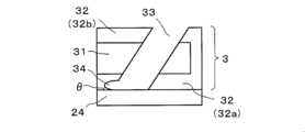
- An optical waveguide 3 is provided on the upper surface of the wiring board 2 via a conductor layer 24 formed on the surface of the wiring board 2 (the surface of the build-up layer 22). As shown in FIG. 2, the optical waveguide 3 includes a core layer 31, a clad layer 32, and a reflection mirror portion 33.
- the core layer 31 included in the optical waveguide 3 acts as an optical path, and the light that has entered the optical waveguide 3 passes through the core layer 31.
- the material forming the core layer 31 is not limited, and is appropriately set in consideration of, for example, light transmission and wavelength characteristics of passing light. Examples of the material include epoxy resin and silicone resin.
- the core layer 31 may have a thickness of, for example, 20 ⁇ m or more and 40 ⁇ m or less.
- the clad layer 32 included in the optical waveguide 3 is formed on both main surfaces of the core layer 31, and in the optical waveguide 3 shown in FIG. 2, the clad layer 32 on the conductor layer 24 side is the lower clad layer 32a, while the other.
- the clad layer 32 of the above is the upper clad layer 32b.
- the material forming the clad layer 32 is not limited, and examples thereof include an epoxy resin and a silicone resin.
- the clad layer 32 may have a thickness of, for example, 5 ⁇ m or more and 60 ⁇ m or less, and the lower clad layer 32a and the upper clad layer 32b may have the same thickness or different thicknesses. ..
- the reflection mirror portion 33 included in the optical waveguide 3 is formed so as to penetrate the upper clad layer 32b, the core layer 31 and the lower clad layer 32a in the thickness direction.
- the reflection mirror portion 33 is not formed parallel to the thickness direction of the optical waveguide 3, but is formed so as to have an inclination with respect to the thickness direction.
- the inclination angle is appropriately set according to the thickness of the optical waveguide 3 and the equipment on which the optical circuit board 1 is mounted.
- the angle formed by the core layer 31 and the reflection mirror portion 33 is about 40 ° or more and 50 ° or less. is there.
- the shape of the opening of the reflection mirror portion 33 is not particularly limited.
- the opening of the reflection mirror portion 33 may be a polygonal shape such as a triangle shape, a square shape, a pentagonal shape, or a hexagonal shape (the polygonal shape includes a polygonal shape having rounded vertices), a circular shape, or an ellipse (the polygonal shape includes a polygonal shape having rounded vertices). It may have a shape such as an oval) shape.
- the opening of the reflection mirror portion 33 has a triangular shape (the triangular shape includes a triangular shape in which each apex is rounded). It is good to have.
- the reflection mirror portion 33 has a recess 34 in at least a part of the clad layer 32 (lower clad layer 32a) on the conductor layer 24 side.
- the thickness direction is a direction extending from the upper surface of the upper clad layer 32b to the lower surface of the lower clad layer 32a.
- the recess 34 is formed so that at least a part of the lower clad layer 32a is recessed in the horizontal plane direction from the reflection mirror portion 33.
- the horizontal plane direction is a direction parallel to the upper surface of the conductor layer 24.
- the interface between the conductor layer 24 and the lower clad layer 32a Is advantageous in that it is difficult to peel off. That is, when stress is applied to the optical waveguide 3, the recess 34 is located at the boundary between the conductor layer 24 and the lower clad layer 32a, which is likely to be the starting point of the peeling, so that the peeling can be reduced.
- the size of the recess 34 is not limited, and for example, the length of the recess 34 in the horizontal plane direction may be about 5 ⁇ m or more and 15 ⁇ m or less.
- the length of the recess 34 in the horizontal plane direction means the length from the reflection mirror portion 33 to the deepest portion of the recess 34 when the recess 34 is viewed from the reflection mirror portion 33 side, and is L1 shown in FIG. 3 (A).
- the length of the recess 34 in the thickness direction may be about 3 ⁇ m or more and 10 ⁇ m or less.
- the length of the recess 34 in the thickness direction means the length of the widest portion of the recess 34 when viewed from the reflection mirror portion 33 side, and corresponds to L2 shown in FIG. 3 (A).
- L1 is larger than L2
- ⁇ shown in FIG. 3A becomes smaller, which is advantageous in that the interface between the conductor layer 24 and the lower clad layer 32a is less likely to be peeled off.
- the recess 34 has a curved portion when the optical waveguide 3 is viewed in cross section in the thickness direction. Since the recess 34 has a curved portion, the stress generated at the boundary between the conductor layer 24 and the lower clad layer 32a can be more dispersed. As a result, the interface between the conductor layer 24 and the lower clad layer 32a becomes more difficult to peel off. Further, the opening of the recess 34 is in contact with the conductor layer 24. In this contact portion, the angle ⁇ formed by the conductor layer 24 and the lower clad layer 32a is an acute angle when the optical waveguide 3 is cross-sectionally viewed in the thickness direction. By making the angle ⁇ an acute angle, it becomes difficult to become a starting point of peeling at the boundary between the conductor layer 24 and the lower clad layer 32a.
- the method of forming the concave portion 34 as in the optical fiber waveguide 3 is not limited, and is formed as follows, for example.
- the conductor layer 24 is formed on the surface of the wiring board 2 (the surface of the build-up layer 22).
- a laminated body (precursor of the optical waveguide) of the core layer 31 and the clad layer 32, which is the material of the optical waveguide 3 is connected to the upper surface of the conductor layer 24.
- the reflection mirror portion 33 is formed on this laminated body.
- the reflection mirror portion 33 is formed by, for example, laser processing.
- the energy of this laser is slightly stronger than usual, specifically, the energy is strengthened to the extent that it reflects off the conductor layer 24 and does not damage the conductor layer 24, thereby forming the reflection mirror portion 33.
- the laser reflected on the conductor layer 24 erodes the lower clad layer 32a to form the recess 34.
- optical circuit board of the present disclosure is not limited to the above-described embodiment.
- the opening of the recess 34 is in contact with the conductor layer 24.
- the opening of the recess does not necessarily have to be in contact with the conductor layer as shown in FIGS. 3B and 3C.
- the angle ⁇ 1 formed by the lower clad layer 32a1 and the conductor layer 241 is a cross-sectional view of the optical waveguide in the thickness direction. It is an acute angle. If the angle ⁇ 1 is an acute angle, as described above, it is unlikely to be the starting point of peeling at the boundary between the conductor layer 241 and the lower clad layer 32a1.
- the opening of the recess 342 is not in contact with the conductor layer 242, and the angle ⁇ 2 formed by the lower clad layer 32a2 and the conductor layer 242 is a cross-sectional view of the optical waveguide in the thickness direction. In some cases it is obtuse. Although the angle ⁇ 2 is an obtuse angle, the recess 342 has a curved portion when the optical waveguide is viewed in cross section in the thickness direction. Since the recess 342 has a curved portion, the stress generated at the boundary between the conductor layer 242 and the lower clad layer 32a2 can be more dispersed as described above. As a result, the interface between the conductor layer 242 and the lower clad layer 32a2 becomes more difficult to peel off.
- the recesses 34, 341, and 342 shown in FIGS. 3 (A) to 3 (C) all have a curved portion when the optical waveguide is viewed in cross section in the thickness direction.
- the recess does not necessarily have to have a curved portion.
- the recess may have a structure other than the curved portion as long as at least a part of the lower clad layer is recessed from the reflection mirror portion in the horizontal plane direction.
- the stress generated at the boundary between the conductor layer and the lower clad layer can be dispersed by providing the recess.
Landscapes
- Physics & Mathematics (AREA)
- Engineering & Computer Science (AREA)
- Microelectronics & Electronic Packaging (AREA)
- General Physics & Mathematics (AREA)
- Optics & Photonics (AREA)
- Optical Integrated Circuits (AREA)
Abstract
本開示に係る光回路基板1は、配線基板2と光導波路3とを含む。光導波路3が、コア層31と、コア層31の両主面に形成されたクラッド層32と、クラッド層32およびコア層31を貫通する反射ミラー部33とを含み、配線基板2の表面に位置する導体層24を介して配線基板2に備えられている。光導波路3を厚み方向に断面視した場合、反射ミラー部33が、導体層24側のクラッド層32(32a)の少なくとも一部に、凹部34を有している。
Description
本開示は、光回路基板に関する。
近年、大容量のデータを高速で通信可能な光通信網が拡大しており、このような光通信網を利用した種々の光通信機器が存在する。このような機器は、例えば特許文献1に記載されるように、基板に光導波路接続された光回路基板が搭載されている。
本開示に係る光回路基板は、配線基板と光導波路とを含む。光導波路が、コア層と、コア層の両主面に形成されたクラッド層と、クラッド層およびコア層を貫通する反射ミラー部とを含み、配線基板の表面に位置する導体層を介して配線基板に備えられている。光導波路を厚み方向に断面視した場合、反射ミラー部が、導体層側のクラッド層の少なくとも一部に、凹部を有している。
光回路基板において、光導波路は配線基板の表面に形成された導体層上に接続されることがある。この場合、配線基板に形成された導体層と光導波路に形成されたクラッド層とが接触することになる。導体層は熱膨張係数が小さい金属で形成されているのに対し、クラッド層は金属に比べて熱膨張係数が大きい樹脂などで形成されている。そのため、熱伸縮差によって、導体層とクラッド層との間が剥離しやすくなる。その結果、光回路基板の安定性や信頼性が低下する。
本開示の配線基板は、光導波路を厚み方向に断面視した場合、反射ミラー部が、導体層側のクラッド層の少なくとも一部に、凹部を有している。そのため、導体層とクラッド層との熱伸縮差が比較的大きくても、導体層とクラッド層との境界に生じる応力が凹部によって分散されやすくなる。その結果、導体層とクラッド層との間が剥離しにくくなり、光回路基板の安定性や信頼性を向上させることができる。
本開示の一実施形態に係る光回路基板を、図1および2に基づいて説明する。図1に示す一実施形態に係る光回路基板1は、配線基板2と光導波路3とを含む。配線基板2は、コア基板21と、コア基板21の両面に積層されたビルドアップ層22とを含む。コア基板21は、絶縁性を有する素材で形成されていれば特に限定されない。絶縁性を有する素材としては、例えば、エポキシ樹脂、ビスマレイミド-トリアジン樹脂、ポリイミド樹脂、ポリフェニレンエーテル樹脂などの樹脂が挙げられる。これらの樹脂は2種以上を混合して用いてもよい。コア基板21の厚みは特に限定されず、例えば100μm以上2000μm以下である。
コア基板21には、補強材が含まれていてもよい。補強材としては、例えば、ガラス繊維、ガラス不織布、アラミド不織布、アラミド繊維、ポリエステル繊維などの絶縁性布材が挙げられる。補強材は2種以上を併用してもよい。さらに、コア基板21には、シリカ、硫酸バリウム、タルク、クレー、ガラス、炭酸カルシウム、酸化チタンなどの無機絶縁性フィラーが、分散されていてもよい。
コア基板21には、コア基板21の上下面を電気的に接続するために、スルーホール導体23が形成されている。スルーホール導体23は、コア基板21の上下面を貫通する孔に形成されている。スルーホール導体23は、例えば、銅めっきなどの金属めっきからなる導体で形成されている。スルーホール導体23は、コア基板21の両面に形成された導体層24に接続されている。形成された導体層24には、ランド(図示せず)が含まれていてもよい。スルーホール導体23は、コア基板21に形成された孔の内壁面のみに形成されていてもよく、コア基板21に形成された孔に充填されていてもよい。
コア基板21の両面には、ビルドアップ層22が積層されている。図1に示す配線基板1では、ビルドアップ層22の構造を詳細に示していないけれども、絶縁層と導体層24とがそれぞれ少なくとも1層交互に積層された構造を有していればよい。
ビルドアップ層22に含まれる絶縁層は、コア基板21と同様、絶縁性を有する素材で形成されていれば特に限定されない。絶縁性を有する素材としては、例えば、エポキシ樹脂、ビスマレイミド-トリアジン樹脂、ポリイミド樹脂、ポリフェニレンエーテル樹脂などの樹脂が挙げられる。これらの樹脂は2種以上を混合して用いてもよい。ビルドアップ層22に絶縁層が2層以上存在する場合、それぞれの絶縁層は、同じ樹脂で形成されていてもよく、異なる樹脂で形成されていてもよい。ビルドアップ層22に含まれる絶縁層とコア基板21とは、同じ樹脂で形成されていてもよく、異なる樹脂で形成されていてもよい。
さらに、ビルドアップ層22に含まれる絶縁層には、シリカ、硫酸バリウム、タルク、クレー、ガラス、炭酸カルシウム、酸化チタンなどの無機絶縁性フィラーが、分散されていてもよい。ビルドアップ層22に含まれる絶縁層の厚みは特に限定されず、例えば5μm以上100μm以下である。ビルドアップ層22に絶縁層が2層以上存在する場合、それぞれの絶縁層は同じ厚みを有していてもよく、異なる厚みを有していてもよい。
ビルドアップ層22に含まれる絶縁層には、層間を電気的に接続するためのビアホール導体25が形成されている。ビアホール導体25は、ビルドアップ層22に含まれる絶縁層の上下面を貫通する孔に形成されている。ビアホール導体25は、例えば、銅めっきなどの金属めっきからなる導体で形成されている。ビアホール導体25は、ビルドアップ層22に含まれる絶縁層の両面に形成された導体層24に接続されている。形成された導体層24には、ランド(図示せず)が含まれていてもよい。ビアホール導体25は、ビルドアップ層22に含まれる絶縁層に形成された孔の内壁面のみに形成されていてもよく、ビルドアップ層22に含まれる絶縁層に形成された孔に充填されていてもよい。
配線基板2の上面には、配線基板2の表面(ビルドアップ層22の表面)に形成された導体層24を介して光導波路3が備えられている。光導波路3は、図2に示すように、コア層31と、クラッド層32と、反射ミラー部33とを含む。
光導波路3に含まれるコア層31は光路として作用し、光導波路3に侵入した光はコア層31を通る。コア層31を形成している材料は限定されず、例えば、光の透過性や通る光の波長特性などを考慮して、適宜設定される。材料としては、例えば、エポキシ樹脂、シリコーン樹脂などが挙げられる。コア層31は、例えば20μm以上40μm以下の厚みを有していてもよい。
光導波路3に含まれるクラッド層32は、コア層31の両主面に形成されており、図2に示す光導波路3では、導体層24側のクラッド層32が下部クラッド層32aであり、他方のクラッド層32が上部クラッド層32bである。クラッド層32を形成している材料は限定されず、例えば、エポキシ樹脂、シリコーン樹脂などが挙げられる。クラッド層32は、例えば5μm以上60μm以下の厚みを有していてもよく、下部クラッド層32aおよび上部クラッド層32bは、同じ厚みを有していてもよく、異なる厚みを有していてもよい。
光導波路3に含まれる反射ミラー部33は、上部クラッド層32b、コア層31および下部クラッド層32aを厚み方向に貫通するように形成されている。反射ミラー部33は、光導波路3の厚み方向と平行に形成されておらず、厚み方向に対して傾斜を有するように形成されている。傾斜角度は、光導波路3の厚みや光回路基板1が搭載される機器などに応じて適宜設定され、例えば、コア層31と反射ミラー部33とのなす角が40°以上50°以下程度である。
反射ミラー部33の開口部の形状、すなわち反射ミラー部33を上部クラッド層32bから平面視した場合の形状は特に限定されない。例えば、反射ミラー部33の開口部は、三角形状、四角形状、五角形状、六角形状などの多角形状(多角形状には、各頂点が丸みを有する多角形状も含む)や、円形状、楕円(長円)形状などの形状を有していてもよい。反射ミラー部33の周囲にビア導体などを形成する領域を十分に確保するために、反射ミラー部33の開口部は三角形状(三角形状には、各頂点が丸みを有する三角形状も含む)を有しているのがよい。
光導波路を厚み方向に断面視した場合、反射ミラー部33は、導体層24側のクラッド層32(下部クラッド層32a)の少なくとも一部に凹部34を有している。厚み方向とは、上部クラッド層32b上面から下部クラッド層32a下面にわたる方向である。凹部34は、反射ミラー部33から下部クラッド層32aの少なくとも一部が水平面方向に窪むように形成されている。水平面方向とは、導体層24上面に平行な方向である。凹部34が、図2に示すように反射ミラー部33の内壁面と導体層24とのなす角度が鋭角である側に位置している場合には、導体層24と下部クラッド層32aとの界面が剥離しにくくなる点で有利である。つまり、光導波路3に応力が加わったときに、導体層24と下部クラッド層32aとの境界において剥離の起点となり易い部分に凹部34が位置していることで剥離を低減することができる。
凹部34の大きさは限定されず、例えば、凹部34の水平面方向の長さは、5μm以上15μm以下程度であってもよい。凹部34の水平面方向の長さとは、凹部34を反射ミラー部33側から見た場合に、反射ミラー部33から凹部34の最深部までの長さを意味し、図3(A)に示すL1に相当する。凹部34の厚み方向の長さは、3μm以上10μm以下程度であってもよい。凹部34の厚み方向の長さとは、凹部34を反射ミラー部33側から見た場合に、最も幅の広い部分の長さを意味し、図3(A)に示すL2に相当する。L1がL2よりも大きい場合には、図3(A)に示すθが小さくなるため導体層24と下部クラッド層32aとの界面が剥離しにくくなる点で有利である。
図2において凹部34は、光導波路3を厚み方向に断面視した場合に湾曲部を有している。凹部34が湾曲部を有することによって、導体層24と下部クラッド層32aとの境界に生じる応力をより分散させることができる。その結果、導体層24と下部クラッド層32aとの界面が、より剥離しにくくなる。さらに、凹部34の開口部は導体層24と接触している。この接触部分において、導体層24と下部クラッド層32aとのなす角θは、光導波路3を厚み方向に断面視した場合に鋭角である。角θを鋭角にすることによって、導体層24と下部クラッド層32aとの境界において剥離の起点となりにくくなる。
光導波路3のように凹部34を形成する方法は限定されず、例えば、次のように形成される。まず、配線基板2の表面(ビルドアップ層22の表面)に導体層24を形成する。次いで、導体層24の上面に、光導波路3の材料となるコア層31とクラッド層32との積層体(光導波路の前駆体)を接続させる。次いで、この積層体に反射ミラー部33を形成する。反射ミラー部33は、例えばレーザ加工によって形成される。このレーザのエネルギーを通常よりも若干強めて、具体的には、導体層24に反射して導体層24にはダメージを与えない程度に強めて、反射ミラー部33を形成する。このように、レーザのエネルギーを通常よりも若干強めて加工することによって、導体層24に反射したレーザが、下部クラッド層32aを浸食して凹部34が形成される。
本開示の光回路基板は、上述の一実施形態に限定されない。例えば、上述の光回路基板1では、図3(A)に示すように凹部34の開口部は導体層24と接触している。しかし、凹部の開口部は、図3(B)および(C)に示すように必ずしも導体層と接触していなくてもよい。
図3(B)では、凹部341の開口部は、導体層241と接触していないものの、下部クラッド層32a1と導体層241とのなす角θ1は、光導波路を厚み方向に断面視した場合に鋭角である。角θ1は鋭角であれば、上述のように、導体層241と下部クラッド層32a1との境界において剥離の起点となりにくくなる。
一方、図3(C)では、凹部342の開口部は、導体層242と接触しておらず、下部クラッド層32a2と導体層242とのなす角θ2は、光導波路を厚み方向に断面視した場合に鈍角である。角θ2が鈍角であるものの、凹部342は、光導波路を厚み方向に断面視した場合に湾曲部を有している。凹部342が湾曲部を有しているため、上述のように、導体層242と下部クラッド層32a2との境界に生じる応力をより分散させることができる。その結果、導体層242と下部クラッド層32a2との界面が、より剥離しにくくなる。
図3(A)~(C)に示す凹部34、341、342は、いずれも光導波路を厚み方向に断面視した場合に湾曲部を有している。しかし、凹部は必ずしも湾曲部を有していなくてもよい。凹部は、反射ミラー部から下部クラッド層の少なくとも一部が水平面方向に窪むように形成されていれば、湾曲部以外の構造であってもよい。本開示の光回路基板は、凹部を設けることによって、導体層と下部クラッド層との境界に生じる応力を分散させることができる。
1 光回路基板
2 配線基板
21 コア基板
22 ビルドアップ層
23 スルーホール導体
24、241、242 導体層
25 ビアホール導体
3 光導波路
31 コア層
32 クラッド層
32a、32a1、32a2 下部クラッド層
32b 上部クラッド層
33 反射ミラー部
34、341、342 凹部
2 配線基板
21 コア基板
22 ビルドアップ層
23 スルーホール導体
24、241、242 導体層
25 ビアホール導体
3 光導波路
31 コア層
32 クラッド層
32a、32a1、32a2 下部クラッド層
32b 上部クラッド層
33 反射ミラー部
34、341、342 凹部
Claims (5)
- 配線基板と光導波路とを含み、
前記光導波路が、コア層と、該コア層の両主面に形成されたクラッド層と、該クラッド層および前記コア層を貫通する反射ミラー部とを含み、前記配線基板の表面に位置する導体層を介して前記配線基板に備えられており、
前記光導波路を厚み方向に断面視した場合、前記反射ミラー部が、前記導体層側の前記クラッド層の少なくとも一部に、凹部を有していることを特徴とする、光回路基板。 - 前記凹部が、前記断面視した場合に湾曲部を有している請求項1に記載の光回路基板。
- 前記光導波路を前記断面視した場合、前記凹部は、前記コア層の下面と前記反射ミラー部の壁面とが鈍角をなしている部分の下側に位置している請求項1または2に記載の光回路基板。
- 前記凹部の開口部が前記導体層と接触しており、接触部分において前記導体層と前記クラッド層とのなす角が、前記断面視した場合に鋭角である請求項1~3のいずれかに記載の光回路基板。
- 前記断面視において、前記凹部の水平面方向の長さは、厚み方向の長さよりも大きい請求項1~4のいずれかに記載の光回路基板。
Priority Applications (2)
| Application Number | Priority Date | Filing Date | Title |
|---|---|---|---|
| US17/439,558 US12038602B2 (en) | 2019-03-15 | 2019-12-17 | Optical circuit substrate |
| JP2021506164A JP7203195B2 (ja) | 2019-03-15 | 2019-12-17 | 光回路基板 |
Applications Claiming Priority (2)
| Application Number | Priority Date | Filing Date | Title |
|---|---|---|---|
| JP2019048624 | 2019-03-15 | ||
| JP2019-048624 | 2019-03-15 |
Publications (1)
| Publication Number | Publication Date |
|---|---|
| WO2020188922A1 true WO2020188922A1 (ja) | 2020-09-24 |
Family
ID=72519028
Family Applications (1)
| Application Number | Title | Priority Date | Filing Date |
|---|---|---|---|
| PCT/JP2019/049295 Ceased WO2020188922A1 (ja) | 2019-03-15 | 2019-12-17 | 光回路基板 |
Country Status (4)
| Country | Link |
|---|---|
| US (1) | US12038602B2 (ja) |
| JP (1) | JP7203195B2 (ja) |
| TW (1) | TWI723697B (ja) |
| WO (1) | WO2020188922A1 (ja) |
Families Citing this family (1)
| Publication number | Priority date | Publication date | Assignee | Title |
|---|---|---|---|---|
| CN114567962B (zh) * | 2020-11-27 | 2023-11-10 | 鹏鼎控股(深圳)股份有限公司 | 电路板的制造方法及电路板 |
Citations (5)
| Publication number | Priority date | Publication date | Assignee | Title |
|---|---|---|---|---|
| JP2003294965A (ja) * | 2002-04-04 | 2003-10-15 | Hitachi Chem Co Ltd | 光導波路デバイス、その製造方法及び基板 |
| JP2004354664A (ja) * | 2003-05-29 | 2004-12-16 | Nec Corp | 光導波路、及びその製造方法 |
| JP2005070158A (ja) * | 2003-08-28 | 2005-03-17 | Ngk Spark Plug Co Ltd | 光導波路基板及びその製造方法 |
| US20080247703A1 (en) * | 2007-04-04 | 2008-10-09 | Ibiden Co., Ltd | Substrate for mounting ic chip and device for optical communication |
| JP2011209510A (ja) * | 2010-03-30 | 2011-10-20 | Kyocera Corp | 光電気配線基板の製造方法 |
Family Cites Families (5)
| Publication number | Priority date | Publication date | Assignee | Title |
|---|---|---|---|---|
| JPH05241044A (ja) | 1992-03-02 | 1993-09-21 | Nippon Telegr & Teleph Corp <Ntt> | 光素子と光導波路との光結合系 |
| JP3147327B2 (ja) * | 1995-07-12 | 2001-03-19 | 日本電信電話株式会社 | 光導波回路及びその製造方法 |
| JP2000171671A (ja) * | 1998-12-09 | 2000-06-23 | Matsushita Electric Ind Co Ltd | 光通信用モジュールおよびその実装方法 |
| JP5462073B2 (ja) | 2010-05-21 | 2014-04-02 | 新光電気工業株式会社 | 光導波路装置及びその製造方法 |
| JP6649076B2 (ja) * | 2015-10-26 | 2020-02-19 | 京セラ株式会社 | 光回路基板の製造方法 |
-
2019
- 2019-12-17 WO PCT/JP2019/049295 patent/WO2020188922A1/ja not_active Ceased
- 2019-12-17 US US17/439,558 patent/US12038602B2/en active Active
- 2019-12-17 JP JP2021506164A patent/JP7203195B2/ja active Active
- 2019-12-24 TW TW108147414A patent/TWI723697B/zh active
Patent Citations (5)
| Publication number | Priority date | Publication date | Assignee | Title |
|---|---|---|---|---|
| JP2003294965A (ja) * | 2002-04-04 | 2003-10-15 | Hitachi Chem Co Ltd | 光導波路デバイス、その製造方法及び基板 |
| JP2004354664A (ja) * | 2003-05-29 | 2004-12-16 | Nec Corp | 光導波路、及びその製造方法 |
| JP2005070158A (ja) * | 2003-08-28 | 2005-03-17 | Ngk Spark Plug Co Ltd | 光導波路基板及びその製造方法 |
| US20080247703A1 (en) * | 2007-04-04 | 2008-10-09 | Ibiden Co., Ltd | Substrate for mounting ic chip and device for optical communication |
| JP2011209510A (ja) * | 2010-03-30 | 2011-10-20 | Kyocera Corp | 光電気配線基板の製造方法 |
Also Published As
| Publication number | Publication date |
|---|---|
| JPWO2020188922A1 (ja) | 2020-09-24 |
| US12038602B2 (en) | 2024-07-16 |
| US20220155518A1 (en) | 2022-05-19 |
| TWI723697B (zh) | 2021-04-01 |
| JP7203195B2 (ja) | 2023-01-12 |
| TW202036064A (zh) | 2020-10-01 |
Similar Documents
| Publication | Publication Date | Title |
|---|---|---|
| JP7032942B2 (ja) | 光導波路および光回路基板 | |
| JP7617248B2 (ja) | 光回路基板およびそれを用いた光学部品実装構造体 | |
| US10168495B1 (en) | Optical waveguide and optical circuit board | |
| TWI622820B (zh) | 光學電路板及其製造方法 | |
| JP2001108853A (ja) | 光配線層、光・電気配線基板及び実装基板 | |
| JP7203195B2 (ja) | 光回路基板 | |
| TWI693437B (zh) | 光波導及光電路基板 | |
| JP6460516B2 (ja) | 光電気混載基板 | |
| WO2022091914A1 (ja) | 光回路基板およびそれを用いた電子部品実装構造体 | |
| US12360322B2 (en) | Optical circuit board | |
| JP6861588B2 (ja) | 伝送線路 | |
| US12130471B2 (en) | Optical element mounting module | |
| JP5300700B2 (ja) | 光配線基板 | |
| JP2020086169A (ja) | 光導波路および光回路基板 | |
| WO2024143134A1 (ja) | 光回路基板、光学部品実装構造体および光回路基板の製造方法 | |
| JP2023008206A (ja) | 配線基板 | |
| JP6882030B2 (ja) | 電子装置 | |
| TWI917915B (zh) | 光迴路基板及安裝構造體 | |
| US20260068047A1 (en) | Wiring substrate and method for manufacturing wiring substrate | |
| JP2021085970A (ja) | 光回路基板 | |
| WO2025206001A1 (ja) | 光回路基板および実装構造体 | |
| TW202314304A (zh) | 光迴路基板及使用該光迴路基板的光學零件安裝構造體 | |
| JP2023111364A (ja) | 伝送構造体および伝送構造体を備える配線基板 | |
| WO2023190186A1 (ja) | 光回路基板 |
Legal Events
| Date | Code | Title | Description |
|---|---|---|---|
| 121 | Ep: the epo has been informed by wipo that ep was designated in this application |
Ref document number: 19919755 Country of ref document: EP Kind code of ref document: A1 |
|
| ENP | Entry into the national phase |
Ref document number: 2021506164 Country of ref document: JP Kind code of ref document: A |
|
| NENP | Non-entry into the national phase |
Ref country code: DE |
|
| 122 | Ep: pct application non-entry in european phase |
Ref document number: 19919755 Country of ref document: EP Kind code of ref document: A1 |