WO2020184508A1 - フィルタ、及び、フィルタの製造方法 - Google Patents
フィルタ、及び、フィルタの製造方法 Download PDFInfo
- Publication number
- WO2020184508A1 WO2020184508A1 PCT/JP2020/009970 JP2020009970W WO2020184508A1 WO 2020184508 A1 WO2020184508 A1 WO 2020184508A1 JP 2020009970 W JP2020009970 W JP 2020009970W WO 2020184508 A1 WO2020184508 A1 WO 2020184508A1
- Authority
- WO
- WIPO (PCT)
- Prior art keywords
- resonator
- wall
- filter
- post
- waveguide
- Prior art date
- Legal status (The legal status is an assumption and is not a legal conclusion. Google has not performed a legal analysis and makes no representation as to the accuracy of the status listed.)
- Ceased
Links
Images



Classifications
-
- H—ELECTRICITY
- H01—ELECTRIC ELEMENTS
- H01P—WAVEGUIDES; RESONATORS, LINES, OR OTHER DEVICES OF THE WAVEGUIDE TYPE
- H01P1/00—Auxiliary devices
- H01P1/20—Frequency-selective devices, e.g. filters
- H01P1/207—Hollow waveguide filters
-
- H—ELECTRICITY
- H01—ELECTRIC ELEMENTS
- H01P—WAVEGUIDES; RESONATORS, LINES, OR OTHER DEVICES OF THE WAVEGUIDE TYPE
- H01P1/00—Auxiliary devices
- H01P1/20—Frequency-selective devices, e.g. filters
- H01P1/207—Hollow waveguide filters
- H01P1/208—Cascaded cavities; Cascaded resonators inside a hollow waveguide structure
- H01P1/2088—Integrated in a substrate
-
- H—ELECTRICITY
- H01—ELECTRIC ELEMENTS
- H01P—WAVEGUIDES; RESONATORS, LINES, OR OTHER DEVICES OF THE WAVEGUIDE TYPE
- H01P3/00—Waveguides; Transmission lines of the waveguide type
- H01P3/12—Hollow waveguides
- H01P3/121—Hollow waveguides integrated in a substrate
Definitions
- the present invention relates to a filter using a post-wall waveguide. It also relates to a method of manufacturing such a filter.
- a plurality of electromagnetically coupled resonators function as a bandpass filter that selectively passes electromagnetic waves in a specific frequency band (hereinafter, also referred to as "passband").
- Patent Document 1 describes a bandpass filter realized by forming a plurality of resonators inside a waveguide.
- a screw is inserted into the resonator, and the center frequency of the pass band can be adjusted by changing the insertion amount of the screw.
- a post-wall waveguide is known as a waveguide that replaces the waveguide.
- the post-wall waveguide is composed of a dielectric substrate, a wide wall covering each of the two main surfaces of the dielectric substrate, and a post wall formed inside the dielectric substrate, and includes the wide wall and the post wall. It is a waveguide in which electromagnetic waves propagate in the area surrounded by.
- the post-wall waveguide has an advantage that it is easy to reduce the weight, height, and cost as compared with the waveguide.
- Non-Patent Document 1 describes a bandpass filter realized by forming a plurality of resonators inside a post-wall waveguide.
- Japanese Patent Publication Japanese Patent Laid-Open No. 8-162805"
- the filter using the post-wall waveguide has a problem that it is difficult to adjust the center frequency of the pass band.
- One aspect of the present invention has been made in view of the above problems, and an object of the present invention is to realize a filter using a post-wall waveguide, in which the center frequency of the pass band can be easily adjusted. It is in.
- the filter according to one aspect of the present invention includes a post-wall waveguide that functions as a resonator group consisting of a plurality of electromagnetically coupled resonators, and the wide wall of the post-wall waveguide includes the resonator.
- a configuration is adopted in which an opening for opening the resonator and an opening for adjusting the center frequency of the pass band is formed.
- FIG. 1 It is a perspective view which shows the structure of the filter which concerns on 1st Embodiment of this invention. It is a partial cross-sectional view of the filter shown in FIG. It is a top view of the post-wall waveguide provided by the filter shown in FIG. It is a graph which shows the frequency characteristic of the transmission coefficient S (2,1) of the filter shown in FIG. Here, the radius of the opening is changed from 100 ⁇ m to 400 ⁇ m in 25 ⁇ m steps.
- FIG. 1 is a perspective view of the filter 1
- FIG. 2 is a partial cross-sectional view of the filter 1.
- the filter 1 includes a post-wall waveguide 11 that functions as a plurality of electromagnetically coupled resonators 11a to 11e.
- the post-wall waveguide 11 includes a dielectric substrate 111, a first wide wall 112 formed on the first main surface (upper surface in FIGS. 1 and 2) of the dielectric substrate 111, and a second main surface of the dielectric substrate 111. It is composed of a second wide wall 113 formed on a surface (lower surface in FIGS. 1 and 2) and a post wall 114 formed inside the dielectric substrate 111.
- the dielectric substrate 111 is a plate-shaped member made of a dielectric material.
- quartz glass is used as the dielectric material constituting the dielectric substrate 111.
- the thickness of the dielectric substrate 111 can be, for example, 500 ⁇ m.
- the first wide wall 112 and the second wide wall 113 are layered (or film-shaped) members made of a conductor material.
- copper is used as the conductor material constituting the first wide wall 112 and the second wide wall 113.
- the post wall 114 is a set of conductor posts arranged in a fence shape that short-circuits the first wide wall 112 and the second wide wall 113.
- the distance between the conductor posts constituting the post wall 114 is sufficiently short compared to the wavelength of the electromagnetic wave input to the post wall waveguide 11, and the post wall 114 functions as a conductor wall for this electromagnetic wave.
- the diameter of the conductor posts can be, for example, 100 ⁇ m, and the spacing between the conductor posts can be, for example, 200 ⁇ m.
- each conductor post constituting the post wall 114 is realized by forming a conductor layer on the inner wall of the through hole penetrating the dielectric substrate 111, or by filling the through hole with a conductor. ..
- the arrangement pattern of the post wall 114 is defined so that the region surrounded by the first wide wall 112, the second wide wall 113, and the post wall 114 functions as a plurality of electromagnetically coupled resonators 11a to 11e. ing.
- the arrangement pattern of the post wall 114 will be described later instead of the reference drawing.
- the first wide wall 112 of the post wall waveguide 11 is formed with the same number of openings 112a to 112e as the resonators 11a to 11e.
- each opening 112x is formed so as to overlap the center of the first wide wall of the corresponding resonator 11x when the first wide wall 112 is viewed in a plan view.
- each resonator 11x has a columnar shape whose height direction is orthogonal to the first wide wall 112, and each opening 112x has a circular shape.
- R1x (hereinafter abbreviated as the radius R1x of the resonator 11x) of the cross section of each resonator 11x (the cross section parallel to the main surface of the dielectric substrate 111) and the radius R2x of the corresponding opening 112x, R2x ⁇ There is a relationship of R1x.
- quartz glass is used as the dielectric material constituting the dielectric substrate 111 of the post wall waveguide 11, but the present invention is not limited to this.
- the dielectric material constituting the dielectric substrate 111 of the post-wall waveguide 11 may be a dielectric material other than quartz, for example, sapphire or alumina.
- copper is used as the conductor material constituting the first wide wall 112 and the second wide wall 113 of the post wall waveguide 11, but the present invention is not limited thereto.
- the conductor material constituting the first wide wall 112 and the second wide wall 113 of the post wall waveguide 11 may be, for example, aluminum or an alloy composed of a plurality of metal elements.
- each resonator 11x has a columnar shape, but the present invention is not limited to this.
- Each resonator 11x may be, for example, a prismatic shape having a regular hexagonal or higher cross section (cross section parallel to the main surface of the dielectric substrate 111).
- each opening 112x has a circular shape, but the present invention is not limited to this.
- Each opening 112x may have, for example, a hexagonal or larger regular polygonal shape.
- the openings 112a to 112e are formed on the first wide wall 112 side, but the present invention is not limited to this. That is, the openings 112a to 112e may be formed on the second wide wall 113 side, or may be dispersedly formed on the first wide wall 112 side and the second wide wall 113 side. As an example, a configuration in which the openings 112a, 112c, 112e are formed on the first wide wall 112 side and the openings 112b, 112d are formed on the second wide wall 113 side is also included in the scope of the present invention.
- the number of resonators 11a to 11e and 112a to 112e is 5 each, but the present invention is not limited to this. That is, the number of the resonators 11a to 11e and the openings 112a to 112e can be any number of two or more.
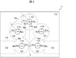
- FIG. 3 is a plan view of the post wall waveguide 11.
- the post wall 114 is shown by a dotted line as a virtual conductor wall.
- the arrangement pattern of the post wall 114 is determined so that the area surrounded by the first wide wall 112, the second wide wall 113, and the post wall 114 includes the following configuration.
- the resonator 11a which is electromagnetically coupled to the input waveguide 11p via the coupling window Apa
- the resonator 11b which is electromagnetically coupled to the resonator 11a via the coupling window Ab
- the resonator 11c which is electromagnetically coupled to the resonator 11b via the coupling window Abc
- the resonator 11d which is electromagnetically coupled to the resonator 11c via the coupling window Acd
- the resonator 11e which is electromagnetically coupled to the resonator 11d via the coupling window Ade
- the output waveguide 11q which is electromagnetically coupled to the resonator 11e via the coupling window Aeq
- the resonators 11a to 11e are columnar, and the input waveguide 11p and the output waveguide 11q are rectangular parallelepiped.
- the distance between the centers of two resonators adjacent to each other is smaller than the sum of the radii of these two resonators.
- the center-to-center distance Dbc of two resonators 11b and 11c adjacent to each other satisfies Dbc ⁇ R1b + R1c. Therefore, the two resonators adjacent to each other are electromagnetically coupled through the coupling window.
- the two resonators adjacent to each other are symmetrical with respect to the plane containing the central axes of these two resonators.
- the two resonators 11b, 11c adjacent to each other are symmetrical with respect to the plane Sbc (see FIG. 3) including the central axes of these two resonators 11b, 11c.
- the resonator group including the resonators 11a to 11e is symmetrical with respect to a specific plane S (see FIG. 3) orthogonal to the first wide wall 112.
- the resonator 11a coupled to the input waveguide 11p and the resonator 11e coupled to the output waveguide 11q are arranged so as to be adjacent to each other, and the resonators 11a to 11e are arranged in an annular shape as a whole. .. Therefore, the size of the dielectric substrate 111 on which the post wall 114 is formed can be reduced. This makes it possible to reduce the absolute value of thermal expansion or contraction of the dielectric substrate 111 that may occur when the environmental temperature changes. Therefore, when the environmental temperature changes, it is possible to suppress a change in the characteristics of the filter 1 that may occur due to thermal expansion or contraction of the dielectric substrate 111.
- the waveguide coupled to the resonator 11a is defined as the input waveguide 11p
- the waveguide coupled to the resonator 11e is defined as the output waveguide 11q, but the present invention is not limited to this.
- the waveguide coupled to the resonator 11a may be used as an output waveguide
- the waveguide coupled to the resonator 11e may be used as an input waveguide.
- the filter 1 includes a post-wall waveguide 11 that functions as a plurality of electromagnetically coupled resonators 11a to 11e. Therefore, the filter 1 functions as a bandpass filter that selectively passes electromagnetic waves belonging to a specific frequency band (hereinafter, “passband”).
- the openings 112a to 112e are used to adjust the center frequency of this passband.
- FIG. 4 is a graph showing the frequency dependence of the transmission coefficient S (2, 1) of the filter 1.
- the material of the dielectric substrate 111 is quartz
- the thickness of the dielectric substrate 111 is 520 ⁇ m
- the radii R1a and R1e of the resonators 11a and 11e are 800 ⁇ m
- the radii R1b to R1d of the resonators 11b to 11d are 840 ⁇ m. The result of the simulation is shown.
- FIG. 4 shows the transmission coefficient S (2,1) of the filter 1 obtained by uniformly changing the radius R2x of each opening 112x from 100 ⁇ m to 400 ⁇ m in 25 ⁇ m steps. According to FIG. 4, it can be seen that as the radius R2x of each opening 112x is increased, the center frequency of the pass band shifts to the high frequency side.
- the center frequency of the pass band is determined according to the size of the openings 112a to 112e. Therefore, when the filter 1 is manufactured, if the step of adjusting the center frequency of the pass band by changing the size of the openings 112a to 112e is performed, the filter 1 whose center frequency of the pass band matches the desired frequency can be obtained. It can be easily manufactured.
- the filter according to the first aspect of the present invention includes a post-wall waveguide that functions as a resonator group consisting of a plurality of electromagnetically coupled resonators, and the wide wall of the post-wall waveguide includes the resonator.
- a configuration is adopted in which an opening for opening the resonator and an opening for adjusting the center frequency of the pass band is formed.
- the center frequency of the pass band can be easily adjusted by changing the size of the aperture.
- the wide wall is said to have the opening formed for each resonator belonging to the resonator.
- the configuration is adopted.
- the center frequency of the pass band can be easily adjusted by changing the size of the aperture.
- the opening is a resonator belonging to the resonator group when the wide wall is viewed in a plan view.
- a configuration is adopted in which the resonator is formed at a position overlapping the center of the resonator opened by the opening.
- the coupling efficiency of the electromagnetic coupling between the resonator and the external space can be improved. Therefore, the adjustment of the center frequency of the pass band by changing the size of the aperture can be performed more effectively.
- the filter according to the fourth aspect of the present invention in addition to the configuration of the filter according to any one of the first to third aspects of the present invention, a configuration in which the opening is circular is adopted.
- the coupling efficiency of the electromagnetic coupling between the resonator and the external space can be improved. Therefore, the adjustment of the center frequency of the pass band by changing the size of the aperture can be performed more effectively.
- the resonator in addition to the configuration of the filter according to any one of the first to fourth aspects of the present invention, the resonator has a columnar shape whose height direction is orthogonal to the wide wall. The configuration is adopted.
- the coupling efficiency of the electromagnetic coupling between the resonator and the external space can be improved. Therefore, the adjustment of the center frequency of the pass band by changing the size of the aperture can be performed more effectively.
- the method for manufacturing the filter device according to the sixth aspect of the present invention is the method for manufacturing the filter according to any one of the first to fifth aspects of the present invention, and the center frequency of the pass band is changed by changing the size of the opening.
- a method that includes a step of adjusting is adopted.
Landscapes
- Control Of Motors That Do Not Use Commutators (AREA)
- Waveguides (AREA)
Abstract
通過帯域の中心周波数を容易に調整することが可能なフィルタを実現する。フィルタ(1)は、電磁気的に結合された複数の共振器(11a~11e)からなる共振器群として機能するポスト壁導波路(11)を備えている。ポスト壁導波路(11)の広壁(第1広壁112)には、共振器群に属する少なくとも1つの共振器(11a~11e)を開放する開口(112a~112e)が形成されている。これらの開口(112a~112e)は、フィルタ(1)の通過帯域の中心周波数を調整するために利用される。
Description
本発明は、ポスト壁導波路を用いたフィルタに関する。また、そのようなフィルタの製造方法に関する。
電磁的に結合された複数の共振器は、特定の周波数帯域(以下、「通過帯域」とも記載する)の電磁波を選択的に通過させるバンドパスフィルタとして機能することが知られている。
例えば、特許文献1には、導波管の内部に複数の共振器を形成することによって実現されたバンドパスフィルタが記載されている。特許文献1に記載のバンドパスフィルタでは、共振器にネジが挿し込まれており、このネジの挿し込み量を変更することによって、通過帯域の中心周波数を調整できるようになっている。
また、導波管に代わる導波路として、ポスト壁導波路が知られている。ポスト壁導波路は、誘電体基板と、誘電体基板の2つの主面の各々を覆う広壁と、誘電体基板の内部に形成されたポスト壁と、により構成され、広壁とポスト壁とに囲まれた領域を電磁波が伝播する導波路である。ポスト壁導波路には、導波管と比べて、軽量化、低背化、低コスト化が容易であるという利点がある。非特許文献1には、ポスト壁導波路の内部に複数の共振器を形成することによって実現されたバンドパスフィルタが記載されている。
Yusuke Uemichi, et. al, Compact and Low-Loss Bandpass Filter Realized in Silica-Based Post-Wall Waveguide for 60-GHz applications, IEEE MTT-S IMS, May 2015.
しかしながら、ポスト壁導波路を用いたフィルタには、通過帯域の中心周波数を調整することが困難であるという問題があった。例えば、ポスト壁導波路を用いたフィルタに、特許文献1に記載の技術を適用して通過帯域の中心周波数を調整することはできない。なぜなら、ポスト壁導波路にネジを挿し込むと、誘電体基板(例えば、石英ガラスにより構成される)が破損するリスクが高いからである。
本発明の一態様は、上記の問題に鑑みてなされたものであり、その目的は、ポスト壁導波路を用いたフィルタであって、通過帯域の中心周波数の調整が容易なフィルタを実現することにある。
本発明の一態様に係るフィルタにおいては、電磁気的に結合された複数の共振器からなる共振器群として機能するポスト壁導波路を備え、前記ポスト壁導波路の広壁には、前記共振器群に属する少なくとも1つの共振器について、当該共振器を開放する開口であって、通過帯域の中心周波数を調整するための開口が形成されている、という構成が採用されている。
本発明の一態様によれば、通過帯域の中心周波数の調整が容易なフィルタを実現することができる。
(フィルタの構成)
本発明の一実施形態に係るフィルタ1の構成について、図1及び図2を参照して説明する。図1は、フィルタ1の斜視図であり、図2は、フィルタ1の部分断面図である。
本発明の一実施形態に係るフィルタ1の構成について、図1及び図2を参照して説明する。図1は、フィルタ1の斜視図であり、図2は、フィルタ1の部分断面図である。
フィルタ1は、電磁気的に結合された複数の共振器11a~11eとして機能するポスト壁導波路11を備えている。
ポスト壁導波路11は、誘電体基板111と、誘電体基板111の第1主面(図1及び図2における上面)に形成された第1広壁112と、誘電体基板111の第2主面(図1及び図2における下面)に形成された第2広壁113と、誘電体基板111の内部に形成されたポスト壁114と、により構成されている。
誘電体基板111は、誘電体材料により構成された板状部材である。本実施形態においては、誘電体基板111を構成する誘電体材料として、石英ガラスを用いている。この場合、誘電体基板111の厚みは、例えば、500μmとすることができる。
第1広壁112及び第2広壁113は、導体材料により構成された層状(又は膜状)部材である。本実施形態においては、第1広壁112及び第2広壁113を構成する導体材料として、銅を用いている。
ポスト壁114は、第1広壁112と第2広壁113とを短絡する、柵状に並んだ導体ポストの集合である。ポスト壁114を構成する導体ポストの間隔は、ポスト壁導波路11に入力される電磁波の波長と比べて十分に短く、ポスト壁114は、この電磁波に対して導体壁として機能する。導体ポストの直径は、例えば、100μmとすることができ、導体ポストの間隔は、例えば、200μmとすることができる。本実施形態において、ポスト壁114を構成する各導体ポストは、誘電体基板111を貫通する貫通孔の内壁に導体層を形成する、或いは、この貫通孔に導体を充填することによって実現されている。ポスト壁114の配置パターンは、第1広壁112、第2広壁113、及びポスト壁114により囲まれた領域が、電磁気的に結合した複数の共振器11a~11eとして機能するように定められている。ポスト壁114の配置パターンについては、参照する図面を代えて後述する。
ポスト壁導波路11の第1広壁112には、共振器11a~11eと同数の開口112a~112eが形成されている。各共振器11x(x=a,b,c,d,e)は、対応する開口112xを介して、ポスト壁導波路11の外部の空間(以下、「外部空間」と記載する)と電磁気的に結合している。すなわち、開口112xは、対応する共振器11xを開放する。共振器11xと外部空間との結合効率を高めるべく、各開口112xの位置は、第1広壁112を平面視したときに、対応する共振器11xの第1広壁の中心と重なるように形成されている。本実施形態において、各共振器11xは、第1広壁112に直交する方向を高さ方向とする円柱状であり、各開口112xは、円形状である。各共振器11xの断面(誘電体基板111の主面と平行な断面)の半径R1x(以下、共振器11xの半径R1xと略記する)と対応する開口112xの半径R2xとの間には、R2x<R1xという関係がある。
なお、本実施形態においては、ポスト壁導波路11の誘電体基板111を構成する誘電体材料として、石英ガラスを用いているが、本発明は、これに限定されない。ポスト壁導波路11の誘電体基板111を構成する誘電体材料は、石英以外の誘電体材料、例えば、サファイアや、アルミナなどでもよい。
また、本実施形態においては、ポスト壁導波路11の第1広壁112及び第2広壁113を構成する導体材料として、銅を用いているが、本発明は、これに限定されない。ポスト壁導波路11の第1広壁112及び第2広壁113を構成する導体材料は、例えば、アルミニウムや、複数の金属元素により構成された合金などでもよい。
また、本実施形態においては、各共振器11xを、円柱状としているが、本発明は、これに限定されない。各共振器11xは、例えば、断面(誘電体基板111の主面と平行な断面)が正六角形以上の正多角形である角柱状でもよい。
また、本実施形態においては、各開口112xを、円形状としているが、本発明は、これに限定されない。各開口112xは、例えば、六角形以上の正多角形状でもよい。
また、本実施形態においては、開口112a~112eを第1広壁112側に形成しているが、本発明は、これに限定されない。すなわち、開口112a~112eは、第2広壁113側に形成されていてもよいし、第1広壁112側と第2広壁113側とに分散して形成されていてもよい。一例として、開口112a,112c,112eが第1広壁112側に形成され、開口112b,112dが第2広壁113側に形成されている構成も、本願発明の範疇に含まれる。
また、本実施形態においては、共振器11a~11e及び112a~112eの個数を各5個としているが、本発明は、これに限定されない。すなわち、共振器11a~11e及び開口112a~112eの個数は、各2個以上の任意の個数であり得る。
(ポスト壁の配置パターン)
ポスト壁導波路11におけるポスト壁114の配置パターンについて、図3を参照して説明する。図3は、ポスト壁導波路11の平面図である。なお、図3においては、ポスト壁114を仮想的な導体壁として点線で図示している。
ポスト壁導波路11におけるポスト壁114の配置パターンについて、図3を参照して説明する。図3は、ポスト壁導波路11の平面図である。なお、図3においては、ポスト壁114を仮想的な導体壁として点線で図示している。
ポスト壁114の配置パターンは、第1広壁112、第2広壁113、及びポスト壁114により囲まれた領域が、以下の構成を含むように決められる。
・入力導波路11p、
・結合窓Apaを介して入力導波路11pと電磁気的に結合された共振器11a、
・結合窓Aabを介して共振器11aと電磁気的に結合された共振器11b、
・結合窓Abcを介して共振器11bと電磁気的に結合された共振器11c、
・結合窓Acdを介して共振器11cと電磁気的に結合された共振器11d、
・結合窓Adeを介して共振器11dと電磁気的に結合された共振器11e、
・結合窓Aeqを介して共振器11eと電磁気的に結合された出力導波路11q、
共振器11a~11eは、円柱状であり、入力導波路11p及び出力導波路11qは、直方体状である。互いに隣接する2つの共振器(例えば、共振器11bと共振器11c)の中心間距離は、これら2つの共振器の半径の和よりも小さい。例えば、互いに隣接する2つの共振器11b,11cの中心間距離Dbcは、Dbc<R1b+R1cを満たす。このため、互いに隣接する2つの共振器が結合窓を介して電磁気的に結合する。
・結合窓Apaを介して入力導波路11pと電磁気的に結合された共振器11a、
・結合窓Aabを介して共振器11aと電磁気的に結合された共振器11b、
・結合窓Abcを介して共振器11bと電磁気的に結合された共振器11c、
・結合窓Acdを介して共振器11cと電磁気的に結合された共振器11d、
・結合窓Adeを介して共振器11dと電磁気的に結合された共振器11e、
・結合窓Aeqを介して共振器11eと電磁気的に結合された出力導波路11q、
共振器11a~11eは、円柱状であり、入力導波路11p及び出力導波路11qは、直方体状である。互いに隣接する2つの共振器(例えば、共振器11bと共振器11c)の中心間距離は、これら2つの共振器の半径の和よりも小さい。例えば、互いに隣接する2つの共振器11b,11cの中心間距離Dbcは、Dbc<R1b+R1cを満たす。このため、互いに隣接する2つの共振器が結合窓を介して電磁気的に結合する。
互いに隣接する2つの共振器は、これら2つの共振器の中心軸を含む平面に対して対称である。例えば、互いに隣接する2つの共振器11b,11cは、これら2つの共振器11b,11cの中心軸を含む平面Sbc(図3参照)に対して対称である。また、共振器11a~11eからなる共振器群は、第1広壁112に直交する特定の平面S(図3参照)に対して対称である。このような対称性をポスト壁114に持たせ、ポスト壁114の配置パターンを規定する独立なパラメータの数を減らすことによって、フィルタ1の設計を容易にすることができる。
また、入力導波路11pに結合した共振器11aと出力導波路11qに結合した共振器11eは、互いに隣接するように配置されており、共振器11a~11eは、全体として環状に並べられている。したがって、ポスト壁114が形成される誘電体基板111のサイズを小さくすることができる。これにより、環境温度が変化したときに生じ得る、誘電体基板111の熱膨張又は熱収縮の絶対値を小さくすることができる。このため、環境温度が変化したときに、誘電体基板111の熱膨張又は熱収縮に起因して生じ得る、フィルタ1の特性変化を抑制することができる。
なお、ここでは、共振器11aに結合された導波路を入力導波路11pとし、共振器11eに結合された導波路を出力導波路11qとしたが、これに限定されない。共振器11aに結合された導波路を出力導波路とし、共振器11eに結合された導波路を入力導波路としてもよい。
(開口の機能)
フィルタ1は、電磁気的に結合した複数の共振器11a~11eとして機能するポスト壁導波路11を備えている。したがって、フィルタ1は、特定の周波数帯域(以下、「通過帯域」)に属する電磁波を選択的に通過させるバンドパスフィルタとして機能する。開口112a~112eは、この通過帯域の中心周波数を調整するために利用される。
フィルタ1は、電磁気的に結合した複数の共振器11a~11eとして機能するポスト壁導波路11を備えている。したがって、フィルタ1は、特定の周波数帯域(以下、「通過帯域」)に属する電磁波を選択的に通過させるバンドパスフィルタとして機能する。開口112a~112eは、この通過帯域の中心周波数を調整するために利用される。
図4は、フィルタ1の透過係数S(2,1)の周波数依存性を示すグラフである。ここでは、誘電体基板111の材料を石英、誘電体基板111の厚みを520μm、共振器11a,11eの半径R1a,R1eを800μm、共振器11b~11dの半径R1b~R1dを840μmと仮定した数値シミュレーションの結果を示す。
図4においては、各開口112xの半径R2xを一律に25μmステップで100μmから400μmまで変化させることにより得られるフィルタ1の透過係数S(2,1)を示している。図4によれば、各開口112xの半径R2xを大きくするほど、通過帯域の中心周波数が高周波側にシフトすることが分かる。
以上のように、フィルタ1においては、通過帯域の中心周波数が開口112a~112eのサイズに応じて決まる。したがって、フィルタ1を製造する際に、開口112a~112eのサイズを変化させることで通過帯域の中心周波数を調整する工程を実施すれば、通過帯域の中心周波数が所望の周波数に一致するフィルタ1を容易に製造することができる。
〔まとめ〕
本発明の態様1に係るフィルタにおいては、電磁気的に結合された複数の共振器からなる共振器群として機能するポスト壁導波路を備え、前記ポスト壁導波路の広壁には、前記共振器群に属する少なくとも1つの共振器について、当該共振器を開放する開口であって、通過帯域の中心周波数を調整するための開口が形成されている、という構成が採用されている。
本発明の態様1に係るフィルタにおいては、電磁気的に結合された複数の共振器からなる共振器群として機能するポスト壁導波路を備え、前記ポスト壁導波路の広壁には、前記共振器群に属する少なくとも1つの共振器について、当該共振器を開放する開口であって、通過帯域の中心周波数を調整するための開口が形成されている、という構成が採用されている。
上記の構成によれば、開口のサイズを変更することによって、通過帯域の中心周波数を容易に調整することができる。
本発明の態様2に係るフィルタにおいては、本発明の態様1に係るフィルタの構成に加えて、前記広壁には、前記共振器に属する各共振器について、前記開口が形成されている、という構成が採用されている。
上記の構成によれば、開口のサイズを変更することによって、通過帯域の中心周波数を容易に調整することができる。
本発明の態様3に係るフィルタにおいては、本発明の態様1又は2に係るフィルタの構成に加えて、前記開口は、前記広壁を平面視したときに、前記共振器群に属する共振器のうち、当該開口により開放される共振器の中心と重なる位置に形成されている、という構成が採用されている。
上記の構成によれば、共振器と外部空間との電磁気的な結合の結合効率を向上させることができる。したがって、開口のサイズを変更することによる通過帯域の中心周波数の調整を、より効果的に行うことができる。
本発明の態様4に係るフィルタにおいては、本発明の態様1~3の何れかに係るフィルタの構成に加えて、前記開口は、円形状である、という構成が採用されている。
上記の構成によれば、共振器と外部空間との電磁気的な結合の結合効率を向上させることができる。したがって、開口のサイズを変更することによる通過帯域の中心周波数の調整を、より効果的に行うことができる。
本発明の態様5に係るフィルタにおいては、本発明の態様1~4の何れかに係るフィルタの構成に加えて、前記共振器は、前記広壁に直交する方向を高さ方向とする円柱状である、という構成が採用されている。
上記の構成によれば、共振器と外部空間との電磁気的な結合の結合効率を向上させることができる。したがって、開口のサイズを変更することによる通過帯域の中心周波数の調整を、より効果的に行うことができる。
本発明の態様6に係るフィルタ装置の製造方法は、本発明の態様1~5の何れかに係るフィルタの製造方法であって、前記開口のサイズを変更することによって、通過帯域の中心周波数を調整する工程を含む、という方法が採用されている。
上記の方法によれば、通過帯域の中心周波数が所望の周波数に一致するフィルタを容易に製造することができる。
〔付記事項〕
本発明は上述した各実施形態に限定されるものではなく、請求項に示した範囲で種々の変更が可能であり、異なる実施形態にそれぞれ開示された技術的手段を適宜組み合わせて得られる実施形態についても本発明の技術的範囲に含まれる。
本発明は上述した各実施形態に限定されるものではなく、請求項に示した範囲で種々の変更が可能であり、異なる実施形態にそれぞれ開示された技術的手段を適宜組み合わせて得られる実施形態についても本発明の技術的範囲に含まれる。
1 フィルタ
11 ポスト壁導波路
111 誘電体基板
112 第1広壁
112a~112e 開口
113 第2広壁
114 ポスト壁
11a~11e 共振器
11 ポスト壁導波路
111 誘電体基板
112 第1広壁
112a~112e 開口
113 第2広壁
114 ポスト壁
11a~11e 共振器
Claims (6)
- 電磁気的に結合された複数の共振器からなる共振器群として機能するポスト壁導波路を備え、
前記ポスト壁導波路の広壁には、前記共振器群に属する少なくとも1つの共振器について、当該共振器を開放する開口であって、通過帯域の中心周波数を調整するための開口が形成されている、
ことを特徴とするフィルタ。 - 前記広壁には、前記共振器に属する各共振器について、前記開口が形成されている、
ことを特徴とする請求項1に記載のフィルタ。 - 前記開口は、前記広壁を平面視したときに、前記共振器群に属する共振器のうち、当該開口により開放される共振器の中心と重なる位置に形成されている、
ことを特徴とする請求項1又は2に記載のフィルタ。 - 前記開口は、円形状である、
ことを特徴とする請求項1~3の何れか1項に記載のフィルタ。 - 前記共振器は、前記広壁に直交する方向を高さ方向とする円柱状である、
ことを特徴とする請求項1~4の何れか1項に記載のフィルタ。 - 請求項1~5の何れか1項に記載のフィルタの製造方法であって、
前記開口のサイズを変更することによって、通過帯域の中心周波数を調整する工程を含む、
ことを特徴とするフィルタの製造方法。
Priority Applications (2)
| Application Number | Priority Date | Filing Date | Title |
|---|---|---|---|
| CN202080012360.7A CN113366699A (zh) | 2019-03-14 | 2020-03-09 | 滤波器及滤波器的制造方法 |
| US17/428,162 US20220029260A1 (en) | 2019-03-14 | 2020-03-09 | Filter and method for manufacture of filter |
Applications Claiming Priority (2)
| Application Number | Priority Date | Filing Date | Title |
|---|---|---|---|
| JP2019047555A JP6720376B1 (ja) | 2019-03-14 | 2019-03-14 | フィルタ、及び、フィルタの製造方法 |
| JP2019-047555 | 2019-03-14 |
Publications (1)
| Publication Number | Publication Date |
|---|---|
| WO2020184508A1 true WO2020184508A1 (ja) | 2020-09-17 |
Family
ID=71402392
Family Applications (1)
| Application Number | Title | Priority Date | Filing Date |
|---|---|---|---|
| PCT/JP2020/009970 Ceased WO2020184508A1 (ja) | 2019-03-14 | 2020-03-09 | フィルタ、及び、フィルタの製造方法 |
Country Status (4)
| Country | Link |
|---|---|
| US (1) | US20220029260A1 (ja) |
| JP (1) | JP6720376B1 (ja) |
| CN (1) | CN113366699A (ja) |
| WO (1) | WO2020184508A1 (ja) |
Citations (3)
| Publication number | Priority date | Publication date | Assignee | Title |
|---|---|---|---|---|
| JPH1093311A (ja) * | 1996-06-10 | 1998-04-10 | Murata Mfg Co Ltd | 誘電体導波管型共振器、誘電体導波管型フィルタ及びその特性調整方法 |
| JP2018191267A (ja) * | 2017-04-28 | 2018-11-29 | 株式会社フジクラ | フィルタ |
| JP2019029898A (ja) * | 2017-08-01 | 2019-02-21 | 株式会社フジクラ | バンドパスフィルタ及び多段バンドパスフィルタ |
Family Cites Families (2)
| Publication number | Priority date | Publication date | Assignee | Title |
|---|---|---|---|---|
| CN101170213B (zh) * | 2007-11-12 | 2011-10-05 | 杭州电子科技大学 | 低轮廓背腔圆环形缝隙一点短路圆极化天线 |
| US9123983B1 (en) * | 2012-07-20 | 2015-09-01 | Hittite Microwave Corporation | Tunable bandpass filter integrated circuit |
-
2019
- 2019-03-14 JP JP2019047555A patent/JP6720376B1/ja not_active Expired - Fee Related
-
2020
- 2020-03-09 US US17/428,162 patent/US20220029260A1/en not_active Abandoned
- 2020-03-09 WO PCT/JP2020/009970 patent/WO2020184508A1/ja not_active Ceased
- 2020-03-09 CN CN202080012360.7A patent/CN113366699A/zh active Pending
Patent Citations (3)
| Publication number | Priority date | Publication date | Assignee | Title |
|---|---|---|---|---|
| JPH1093311A (ja) * | 1996-06-10 | 1998-04-10 | Murata Mfg Co Ltd | 誘電体導波管型共振器、誘電体導波管型フィルタ及びその特性調整方法 |
| JP2018191267A (ja) * | 2017-04-28 | 2018-11-29 | 株式会社フジクラ | フィルタ |
| JP2019029898A (ja) * | 2017-08-01 | 2019-02-21 | 株式会社フジクラ | バンドパスフィルタ及び多段バンドパスフィルタ |
Also Published As
| Publication number | Publication date |
|---|---|
| JP6720376B1 (ja) | 2020-07-08 |
| US20220029260A1 (en) | 2022-01-27 |
| JP2020150464A (ja) | 2020-09-17 |
| CN113366699A (zh) | 2021-09-07 |
Similar Documents
| Publication | Publication Date | Title |
|---|---|---|
| US11955680B2 (en) | Waveguide filter | |
| US7573639B2 (en) | Terahertz-band optical filter, designing method thereof, and manufacturing method thereof | |
| JP4758942B2 (ja) | デュアルバンド共振器およびデュアルバンドフィルタ | |
| US20210126332A1 (en) | Filter | |
| US8884723B2 (en) | TE011 cavity filter assembly | |
| CN103367846A (zh) | 介质谐振滤波器及其制造方法和使用其的双工器/多工器 | |
| CN104064840B (zh) | 小型化带阻型频率选择表面 | |
| CN108574473A (zh) | 共振器和用于提供共振器的方法 | |
| JP2019012977A (ja) | 積層型電子部品 | |
| EP3583656B1 (en) | A microwave resonator, a microwave filter and a microwave multiplexer | |
| CN114430873B (zh) | 波导管滤波器 | |
| EP3667811B1 (en) | Dielectric filter, array antenna device | |
| JP6720376B1 (ja) | フィルタ、及び、フィルタの製造方法 | |
| JP6720374B1 (ja) | フィルタ、及び、フィルタの製造方法 | |
| KR101616768B1 (ko) | 너치가 형성된 유전체 도파관 필터 | |
| CN102468817A (zh) | 微机电滤波器 | |
| JP6720375B1 (ja) | フィルタ、及び、フィルタの製造方法 | |
| US11121443B2 (en) | Bandpass filter | |
| RU2619137C2 (ru) | Многослойный полосно-пропускающий фильтр | |
| JP6680929B1 (ja) | フィルタ装置 | |
| Hong et al. | Reconfigurable angle-selective surface based on 3-D frequency-selective structures | |
| JP6652670B1 (ja) | フィルタ装置 | |
| RU2687878C1 (ru) | Полосно-пропускающая частотно-селективная поверхность | |
| KR101140799B1 (ko) | 타원형 필터 | |
| JP4411315B2 (ja) | 帯域阻止フィルタ |
Legal Events
| Date | Code | Title | Description |
|---|---|---|---|
| 121 | Ep: the epo has been informed by wipo that ep was designated in this application |
Ref document number: 20769943 Country of ref document: EP Kind code of ref document: A1 |
|
| NENP | Non-entry into the national phase |
Ref country code: DE |
|
| 122 | Ep: pct application non-entry in european phase |
Ref document number: 20769943 Country of ref document: EP Kind code of ref document: A1 |