WO2020183617A1 - 感光性樹脂組成物、パターン硬化膜及びその製造方法、半導体素子並びに電子デバイス - Google Patents
感光性樹脂組成物、パターン硬化膜及びその製造方法、半導体素子並びに電子デバイス Download PDFInfo
- Publication number
- WO2020183617A1 WO2020183617A1 PCT/JP2019/010057 JP2019010057W WO2020183617A1 WO 2020183617 A1 WO2020183617 A1 WO 2020183617A1 JP 2019010057 W JP2019010057 W JP 2019010057W WO 2020183617 A1 WO2020183617 A1 WO 2020183617A1
- Authority
- WO
- WIPO (PCT)
- Prior art keywords
- group
- meth
- acrylate
- resin composition
- photosensitive resin
- Prior art date
- Legal status (The legal status is an assumption and is not a legal conclusion. Google has not performed a legal analysis and makes no representation as to the accuracy of the status listed.)
- Ceased
Links
Images


Classifications
-
- G—PHYSICS
- G03—PHOTOGRAPHY; CINEMATOGRAPHY; ANALOGOUS TECHNIQUES USING WAVES OTHER THAN OPTICAL WAVES; ELECTROGRAPHY; HOLOGRAPHY
- G03F—PHOTOMECHANICAL PRODUCTION OF TEXTURED OR PATTERNED SURFACES, e.g. FOR PRINTING, FOR PROCESSING OF SEMICONDUCTOR DEVICES; MATERIALS THEREFOR; ORIGINALS THEREFOR; APPARATUS SPECIALLY ADAPTED THEREFOR
- G03F7/00—Photomechanical, e.g. photolithographic, production of textured or patterned surfaces, e.g. printing surfaces; Materials therefor, e.g. comprising photoresists; Apparatus specially adapted therefor
- G03F7/004—Photosensitive materials
-
- G—PHYSICS
- G03—PHOTOGRAPHY; CINEMATOGRAPHY; ANALOGOUS TECHNIQUES USING WAVES OTHER THAN OPTICAL WAVES; ELECTROGRAPHY; HOLOGRAPHY
- G03F—PHOTOMECHANICAL PRODUCTION OF TEXTURED OR PATTERNED SURFACES, e.g. FOR PRINTING, FOR PROCESSING OF SEMICONDUCTOR DEVICES; MATERIALS THEREFOR; ORIGINALS THEREFOR; APPARATUS SPECIALLY ADAPTED THEREFOR
- G03F7/00—Photomechanical, e.g. photolithographic, production of textured or patterned surfaces, e.g. printing surfaces; Materials therefor, e.g. comprising photoresists; Apparatus specially adapted therefor
- G03F7/004—Photosensitive materials
- G03F7/022—Quinonediazides
-
- G—PHYSICS
- G03—PHOTOGRAPHY; CINEMATOGRAPHY; ANALOGOUS TECHNIQUES USING WAVES OTHER THAN OPTICAL WAVES; ELECTROGRAPHY; HOLOGRAPHY
- G03F—PHOTOMECHANICAL PRODUCTION OF TEXTURED OR PATTERNED SURFACES, e.g. FOR PRINTING, FOR PROCESSING OF SEMICONDUCTOR DEVICES; MATERIALS THEREFOR; ORIGINALS THEREFOR; APPARATUS SPECIALLY ADAPTED THEREFOR
- G03F7/00—Photomechanical, e.g. photolithographic, production of textured or patterned surfaces, e.g. printing surfaces; Materials therefor, e.g. comprising photoresists; Apparatus specially adapted therefor
- G03F7/20—Exposure; Apparatus therefor
Definitions
- the present invention relates to a photosensitive resin composition, a pattern cured film and a method for producing the same, a semiconductor element, and an electronic device.
- insulating layers such as interlayer insulating layers and surface protective layers of semiconductor elements are required to have better electrical characteristics, heat resistance, mechanical characteristics and the like. ..
- a photosensitive resin composition containing an alkali-soluble resin has been developed (see, for example, Patent Documents 1, 2 and 3).
- a patterned resin film is obtained by applying and drying these photosensitive resin compositions on a substrate to form a resin film, and exposing and developing the resin film. Then, the pattern-cured film (pattern-formed cured film) can be formed by heat-curing the pattern resin film, and the pattern-cured film can be used as a surface protective layer and an interlayer insulating layer.
- the package substrate there is a form in which wiring is formed on the cured film with a metal such as copper.
- the cured film formed by using the conventional photosensitive resin composition may be peeled off between the cured film and the copper wiring due to the influence of heat damage during the reflow process, and the subsequent temperature cycle test May cause disconnection, package cracks, etc. Therefore, it has been studied to add an imide compound having excellent heat resistance to the photosensitive resin composition (see, for example, Patent Document 4).
- the imide compound Since the imide compound has low alkali solubility, problems tend to occur in patterning property such as undissolved residue in the exposed portion of the resin film after development. Further, since the imide compound has low compatibility with an alkali-soluble resin such as a phenol resin, the photosensitive resin composition becomes cloudy, and it is difficult to obtain a fine pattern resin film. Therefore, there is a demand for a photosensitive resin composition that can achieve both microfabrication and reflow heat resistance.
- a main object of the present invention is to provide a photosensitive resin composition capable of forming a pattern-cured film having resolvability capable of microfabrication and excellent reflow heat resistance.
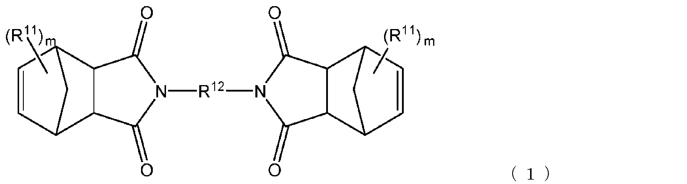
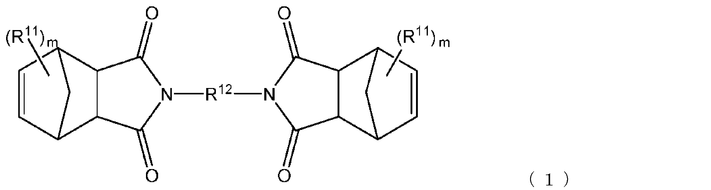
- One aspect of the present invention provides a photosensitive resin composition containing an alkali-soluble resin, a nadiimide-based compound represented by the following formula (1), a heat-crosslinking agent, and a compound that generates an acid by light. To do.
- R 11 independently represents an allyl group, m is 0 or 1, and R 12 represents a divalent organic group.
- the present invention provides a pattern-cured film having a pattern on another aspect, the pattern containing a cured product of a resin film composed of the above-mentioned photosensitive resin composition.
- the present invention also applies a step of applying the above-mentioned photosensitive resin composition to a part or all of a substrate to form a resin film, a step of exposing a part or all of the resin film, and a step of exposing the exposed resin film.
- a method for producing a pattern cured film comprising a step of developing with an alkaline aqueous solution to form a pattern resin film and a step of heating the pattern resin film.
- a semiconductor device including the above-mentioned pattern curing film as an interlayer insulating layer or a surface protective layer is provided.
- an electronic device comprising the above semiconductor device is provided.
- a photosensitive resin composition capable of forming a pattern cured film having a resolution capable of microfabrication and excellent reflow heat resistance. Further, according to the present invention, it is possible to provide a pattern cured film using the photosensitive resin composition, a method for producing the same, a semiconductor element, and an electronic device.
- (meth) acrylic acid means "acrylic acid” or “methacrylic acid”, as is the case with other similar expressions such as (meth) acrylate.
- the photosensitive resin composition includes an alkali-soluble resin (hereinafter, may be referred to as “component (A)”) and a nadiimide-based compound represented by the formula (1) (hereinafter, “(B)). It may be referred to as “component”), a heat-crosslinking agent (hereinafter, may be referred to as "(C) component”), and a compound that generates an acid by light (hereinafter, may be referred to as "(D) component”). ) And.
- component (A) alkali-soluble resin
- component (B) nadiimide-based compound represented by the formula (1)
- component a heat-crosslinking agent
- (D) component a compound that generates an acid by light
- the photosensitive resin composition can be suitably used as a positive photosensitive resin composition.
- the form of the positive photosensitive resin composition will be described in detail.
- the alkali-soluble resin means a resin that is soluble in an aqueous alkaline solution (developing solution).
- the alkaline aqueous solution is an alkaline solution such as a tetramethylammonium hydroxide (TMAH) aqueous solution, a metal hydroxide aqueous solution, or an organic amine aqueous solution.
- TMAH tetramethylammonium hydroxide
- a TMAH aqueous solution having a concentration of 2.38% by mass is used for development. It can be confirmed, for example, that the component (A) is soluble in an alkaline developer as follows.
- a varnish obtained by dissolving a resin in an arbitrary solvent is spin-coated on a substrate such as a silicon wafer to form a coating film having a film thickness of about 5 ⁇ m.
- a substrate such as a silicon wafer
- This is immersed in any of a TMAH aqueous solution, a metal hydroxide aqueous solution, or an organic amine aqueous solution at 20 to 25 ° C.
- the resin can be regarded as soluble in the alkaline developer.
- the component (A) may be a resin having a phenolic hydroxyl group.
- the resin having a phenolic hydroxyl group include hydroxystyrene resin, phenol resin, polybenzoxazole precursor such as poly (hydroxyamide), poly (hydroxyphenylene) ether, and polynaphthol.
- the component (A) may be composed of only one of these resins, or may be composed of two or more of them.
- the component (A) may contain a hydroxystyrene resin because of its excellent electrical properties (insulating properties) and small volume shrinkage during curing.
- the hydroxystyrene resin has a structural unit represented by the following formula (21).
- R 21 represents a hydrogen atom or a methyl group
- R 22 represents an alkyl group having 1 to 10 carbon atoms, an aryl group having 6 to 10 carbon atoms or an alkoxy group having 1 to 10 carbon atoms
- a Indicates an integer of 0 to 3
- b indicates an integer of 1 to 3. The total of a and b is 5 or less.
- the hydroxystyrene resin can be obtained by polymerizing a monomer or the like that gives a structural unit represented by the formula (21).
- Examples of the alkyl group having 1 to 10 carbon atoms represented by R 22 include a methyl group, an ethyl group, a propyl group, a butyl group, a pentyl group, a hexyl group, a heptyl group, an octyl group, a nonyl group and a decyl group. .. These groups may be linear or branched.
- Examples of the aryl group having 6 to 10 carbon atoms represented by R 22 include a phenyl group and a naphthyl group.
- Examples of the alkoxy group having 1 to 10 carbon atoms represented by R 22 include a methoxy group, an ethoxy group, a propoxy group, a butoxy group, a pentoxy group, a hexoxy group, a heptoxy group, an octoxy group, a nonoxy group and a decoxy group. .. These groups may be linear or branched.
- Examples of the monomer giving the structural unit represented by the formula (21) include p-hydroxystyrene, m-hydroxystyrene, o-hydroxystyrene, p-isopropenylphenol, m-isopropenylphenol and o-isopropenylphenol. Can be mentioned. These monomas can be used alone or in combination of two or more.
- Hydroxystyrene resin is not limited by its manufacturing method.
- the hydroxyl group of the monomer giving the structural unit represented by the formula (21) is protected by a tert-butyl group, an acetyl group, or the like to form a hydroxyl group-protected monoma, and the hydroxyl group-protected monoma.
- the hydroxystyrene resin may be a homopolymer of a monomer giving a structural unit represented by the formula (21), and a copolymer of a monomer giving a structural unit represented by the formula (21) and another monomer may be used. It may be a polymer.
- the ratio of the structural unit represented by the formula (21) in the copolymer constitutes the component (A) from the viewpoint of the solubility of the exposed portion in the alkaline developing solution. It may be 10 to 100 mol%, 20 to 97 mol%, 30 to 95 mol%, or 50 to 95 mol% based on the total molar amount of all the components to be added.
- the hydroxystyrene resin may further have a structural unit represented by the following formula (22) from the viewpoint of improving the dissolution inhibition of the unexposed portion in the alkaline developer.
- R 23 represents a hydrogen atom or a methyl group
- R 24 represents an alkyl group having 1 to 10 carbon atoms, an aryl group having 6 to 10 carbon atoms or an alkoxy group having 1 to 10 carbon atoms
- c Indicates an integer from 0 to 3.
- Examples of the alkyl group having 1 to 10 carbon atoms, the aryl group having 6 to 10 carbon atoms, and the alkoxy group having 1 to 10 carbon atoms represented by R 24 include the same groups as those of R 22 .
- the alkali-soluble resin having the structural unit represented by the formula (22) can be obtained by using a monoma giving the structural unit represented by the formula (22).
- the monoma giving the structural unit represented by the formula (22) include styrene, ⁇ -methylstyrene, o-methylstyrene, m-methylstyrene, p-methylstyrene, o-methoxystyrene, m-methoxystyrene, and the like.
- Aromatic vinyl compounds such as p-methoxystyrene can be mentioned. These monomas can be used alone or in combination of two or more.
- the hydroxystyrene resin is an alkali-soluble resin having a structural unit represented by the formula (22)
- the formula (22) is used from the viewpoint of inhibition of dissolution of the unexposed portion in the alkaline developer and water absorption of the cured film.
- the ratio of the structural unit represented is 1 to 90 mol%, 3 to 80 mol%, 5 to 70 mol%, or 5 to 50 mol% based on the total molar amount of all the components constituting the component (A). It may be there.
- the hydroxystyrene resin may have a structural unit based on a (meth) acrylic acid ester from the viewpoint of lowering the elastic modulus.
- the (meth) acrylic acid ester may be a compound having an alkyl group or a hydroxyalkyl group.
- Examples of the (meth) acrylic acid ester include methyl (meth) acrylic acid, ethyl (meth) acrylic acid, propyl (meth) acrylic acid, butyl (meth) acrylic acid, pentyl (meth) acrylic acid, and (meth) acrylic acid.
- (Meta) acrylic acid alkyl esters such as hexyl acid, heptyl (meth) acrylate, octyl (meth) acrylate, nonyl (meth) acrylate, decyl (meth) acrylate; and hydroxymethyl (meth) acrylate, ( Hydroxyethyl acrylate, (meth) hydroxypropyl acrylate, (meth) hydroxybutyl acrylate, (meth) hydroxypentyl acrylate, (meth) hydroxyhexyl acrylate, (meth) hydroxyheptyl acrylate, (meth) Examples thereof include (meth) acrylic acid hydroxyalkyl esters such as hydroxyoctyl acrylate, (meth) acrylic acid hydroxynonyl, and (meth) acrylic acid hydroxydecyl. These monomas can be used alone or in combination of two or more.
- the ratio of the structural unit based on (meth) acrylic acid ester is (A) from the viewpoint of the mechanical properties of the pattern cured film. ) It may be 1 to 90 mol%, 3 to 80 mol%, 5 to 70 mol%, or 5 to 50 mol% based on the total molar amount of all the components constituting the component.
- the component (A) may contain a phenol resin and may contain a novolak type phenol resin.
- Phenolic resin is a polycondensation product of phenol or its derivatives and aldehydes. Polycondensation is usually carried out in the presence of a catalyst such as an acid or base.
- the phenolic resin obtained when an acid catalyst is used is particularly called a novolak type phenolic resin.
- the novolak type phenol resin include phenol / formaldehyde novolak resin, cresol / formaldehyde novolak resin, xylenol / formaldehyde novolak resin, resorcinol / formaldehyde novolak resin, and phenol-naphthol / formaldehyde novolak resin.
- Examples of the phenol derivative constituting the phenol resin include o-cresol, m-cresol, p-cresol, o-ethylphenol, m-ethylphenol, p-ethylphenol, o-butylphenol, m-butylphenol and p-butylphenol.
- aldehydes constituting the phenol resin include formaldehyde, acetaldehyde, furfural, benzaldehyde, hydroxybenzaldehyde, methoxybenzaldehyde, hydroxyphenylacetaldehyde, methoxyphenylacetaldehyde, crotonaldehyde, chloroacetaldehyde, chlorophenylacetaldehyde, glyceraldehyde, and glyoxylic acid.
- Examples thereof include methyl glyoxylate, phenyl glyoxylate, hydroxyphenyl glyoxylate, formylacetic acid, methylformylacetate, 2-formylpropionic acid, and methyl 2-formylpropionicate. These may be used individually by 1 type or in combination of 2 or more type.
- formaldehyde precursors such as paraformaldehyde and trioxane
- ketone compounds such as acetone, pyruvic acid, levulinic acid, 4-acetylbutyl acid, acetonedicarboxylic acid, and 3,3'-4,4'-benzophenonetetracarboxylic acid can be used. It may be used in the reaction.
- the weight average molecular weight (Mw) of the component (A) is preferably 1000 to 500,000, more preferably 2000 to 200,000, and more preferably 2000 to 100,000, considering the balance between the solubility in an alkaline aqueous solution, the photosensitive property, and the mechanical property of the cured film. More preferred. Mw is a value obtained by measuring by a gel permeation chromatography (GPC) method and converting from a standard polystyrene calibration curve.
- GPC gel permeation chromatography
- the nadiimide compound as the component (B) has a structural unit represented by the following formula (1), so that an effect of improving thermal stability can be obtained and the compatibility with the component (A) is high.
- R 11 independently represents an allyl group, m is 0 or 1, and R 12 represents a divalent organic group.
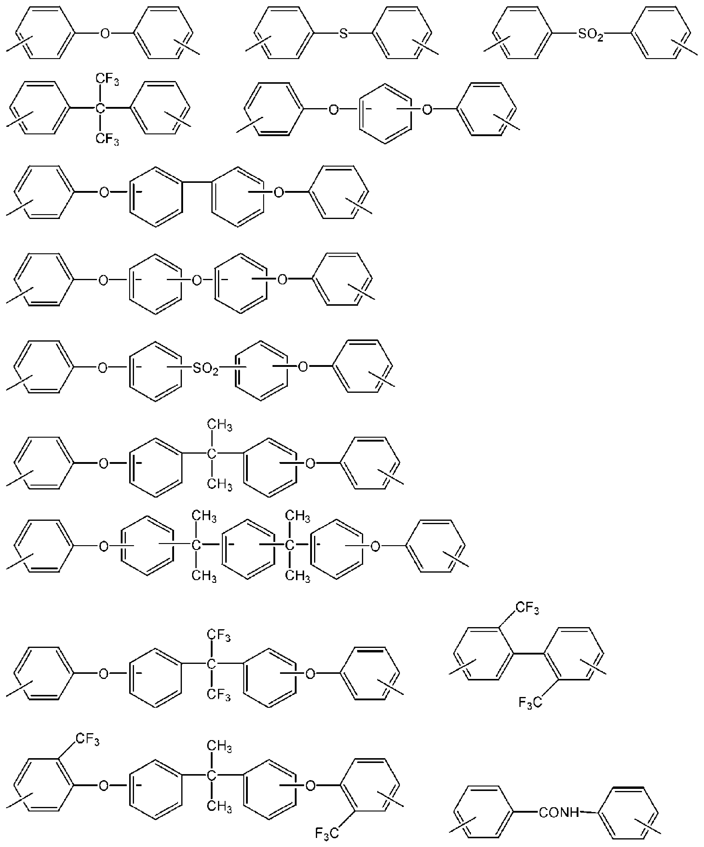
- the divalent organic group represented by R 12 may have an aromatic hydrocarbon group (aromatic ring).
- aromatic hydrocarbon groups include benzene residues, toluene residues, xylene residues, and naphthalene residues.
- the divalent organic group may have a linear, branched or cyclic aliphatic hydrocarbon group.
- the aliphatic hydrocarbon group may be a linear, branched or cyclic alkyl group.
- the divalent organic group may have both an aromatic hydrocarbon group and an aliphatic hydrocarbon group.
- the divalent organic group represented by R 12 may be a divalent hydrocarbon group containing only a carbon atom and a hydrogen atom, and may be a divalent organic group containing other atoms in addition to the carbon atom and the hydrogen atom. There may be.
- R 12 is preferably a divalent hydrocarbon group.
- the divalent hydrocarbon group may have an aliphatic hydrocarbon group.
- the aliphatic hydrocarbon group is preferably an alkylene group having 1 to 10 carbon atoms, more preferably an alkylene group having 1 to 8 carbon atoms, and further preferably an alkylene group having 1 to 5 carbon atoms. ..
- the divalent hydrocarbon group may be a divalent hydrocarbon group having an aromatic hydrocarbon group, and the divalent hydrocarbon having any of the following structures. It may be a hydrocarbon group.
- the divalent organic group including other atoms may contain atoms such as nitrogen atom, oxygen atom, sulfur atom and fluorine atom in addition to carbon atom and hydrogen atom.
- the divalent organic group containing other atoms is preferably a divalent hydrocarbon group having any of the following structures.
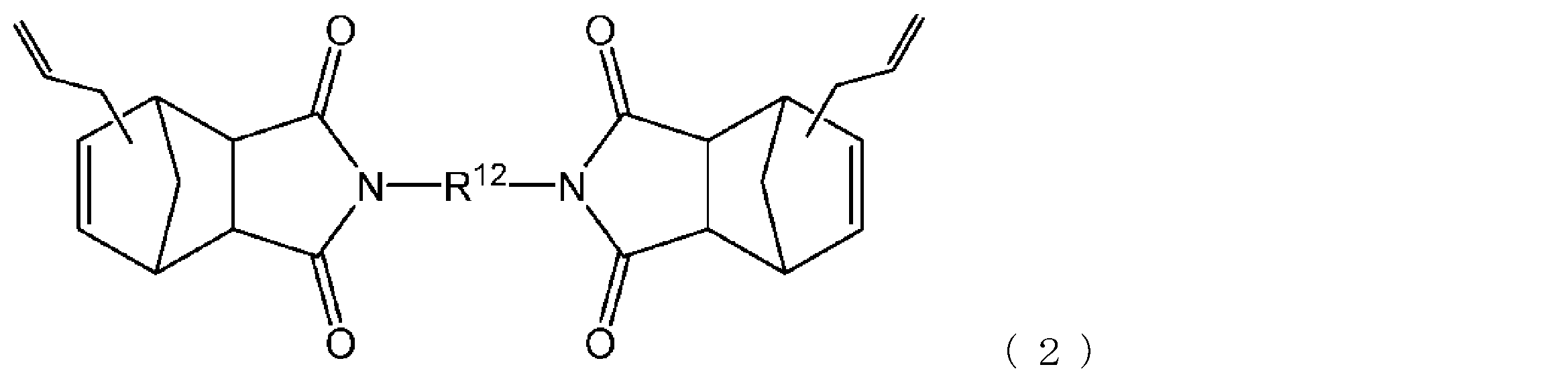
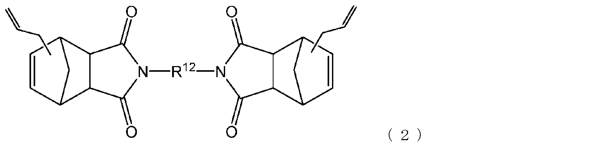
- the nadiimide compound is preferably a bisallyl nadiimide compound represented by the following formula (2) (a compound in which m is 1 in the formula (1)).
- R 12 is synonymous with R 12 in equation (1).
- the content of the component (B) is preferably 1 to 90 parts by mass, more preferably 3 to 80 parts by mass, and 5 to 70 parts by mass with respect to 100 parts by mass of the component (A) from the viewpoint of improving resolution. Is more preferable, and 10 to 60 parts by mass is particularly preferable.
- the cross-linking agent as the component (C) is a compound having a group capable of forming a bridging structure (cross-linking structure) by reacting with the component (A) when the resin film after pattern formation is heated and cured. .. As a result, the brittleness of the resin film and the melting of the resin film can be prevented.
- the component (C) include a compound having two or more alkoxymethyl groups and a compound having two or more epoxy groups.
- the component (C) may be a compound having two or more alkoxymethyl groups from the viewpoint of excellent balance between the effect of promoting dissolution of the exposed portion and the effect of preventing melting of the resin film during curing after pattern formation.
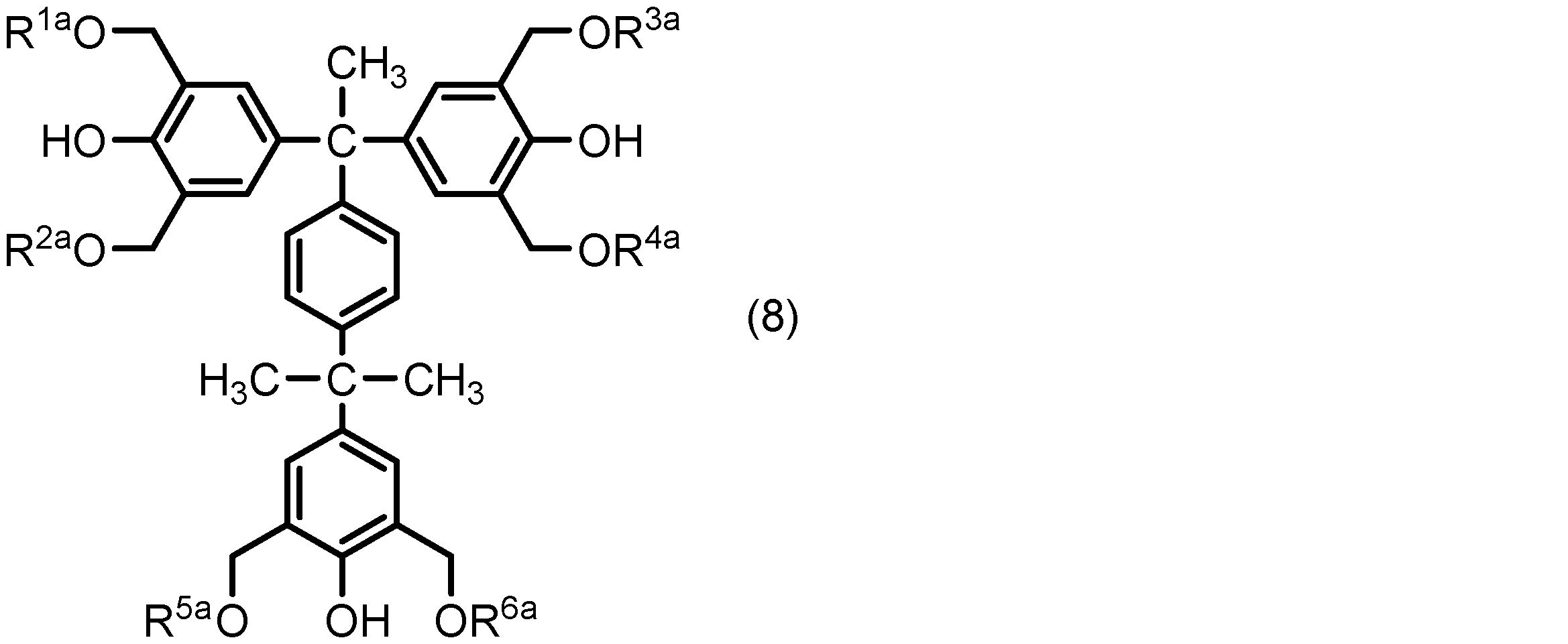
- the compound having two or more alkoxymethyl groups is not particularly limited, and may be, for example, a compound represented by the following formula (7) or a compound represented by the following formula (8).
- R 1 to R 6 each independently represent an alkyl group having 1 to 10 carbon atoms.
- the alkyl group having 1 to 10 carbon atoms the same group as R 22 can be exemplified.
- the number of carbon atoms of the alkyl group may be 1 to 5, 1 to 3, 1 or 2, or 1.
- R 1a to R 6a independently represent alkyl groups having 1 to 10 carbon atoms.
- the alkyl group having 1 to 10 carbon atoms the same group as R 22 can be exemplified.
- the number of carbon atoms of the alkyl group may be 1 to 5, 1 to 3, 1 or 2, or 1.
- the compound having two or more epoxy groups is not particularly limited.
- Examples of the compound having an epoxy group include bisphenol A type epoxy compound, bisphenol F type epoxy compound, phenol novolac type epoxy compound, cresol novolac type epoxy compound, alicyclic epoxy compound, glycidylamine type epoxy compound, and heterocyclic epoxy.
- Examples include compounds, halogenated epoxy compounds, and polyalkylene glycol diglycidyl ethers. These may be used individually by 1 type or in combination of 2 or more type.
- the content of the component (C) is 0.5 to 50 parts by mass and 1 to 40 parts by mass with respect to 100 parts by mass of the component (A) from the viewpoint of improving the heat resistance of the cured film and reducing the residual stress. It may be 2 to 30 parts by mass or 5 to 25 parts by mass.
- Component (D) Compound that produces acid by light>
- the component (D) has a function of generating an acid by receiving light irradiation and increasing the solubility of the light-irradiated portion in an alkaline aqueous solution.
- a compound generally called a photoacid generator can be used as the component (D).
- Specific examples of the component (D) include an o-quinone diazonium compound, an aryldiazonium salt, a diallyl iodonium salt and a triarylsulfonium salt.
- the component (D) may contain only one of these compounds, or may contain two or more of them. Among these, the component (D) may be an o-quinone diazide compound because of its high sensitivity.
- o-quinone diazide compound for example, a compound obtained by condensing an o-quinone diazidosulfonyl chloride with a hydroxy compound, an amino compound or the like in the presence of a dehydrochloric acid agent can be used.
- o-quinone diazide sulfonyl chloride examples include benzoquinone-1,2-diazide-4-sulfonyl chloride, naphthoquinone-1,2-diazide-5-sulfonyl chloride, and naphthoquinone-1,2-diazide-6-sulfonyl chloride. Can be mentioned.
- hydroxy compound examples include hydroquinone, resorcinol, pyrogallol, bisphenol A, bis (4-hydroxyphenyl) methane, 1,1-bis (4-hydroxyphenyl) -1- [4- ⁇ 1- (4-hydroxyphenyl).
- amino compound examples include p-phenylenediamine, m-phenylenediamine, 4,4'-diaminodiphenyl ether, 4,4'-diaminodiphenylmethane, 4,4'-diaminodiphenyl sulfone, and 4,4'-diaminodiphenyl sulfide.
- O-aminophenol O-aminophenol, m-aminophenol, p-aminophenol, 3,3'-diamino-4,4'-dihydroxybiphenyl, 4,4'-diamino-3,3'-dihydroxybiphenyl, bis (3-) Amino-4-hydroxyphenyl) propane, bis (4-amino-3-hydroxyphenyl) propane, bis (3-amino-4-hydroxyphenyl) sulfone, bis (4-amino-3-hydroxyphenyl) sulfone, bis (4-amino-3-hydroxyphenyl) Examples thereof include 3-amino-4-hydroxyphenyl) hexafluoropropane and bis (4-amino-3-hydroxyphenyl) hexafluoropropane.
- the o-quinone diazide compound is 1,1-bis (4-bis) (4-) from the viewpoint of reactivity when synthesizing the o-quinone diazide compound and from the viewpoint of an appropriate absorption wavelength range when exposing the resin film.
- dehydrochloric acid agent examples include sodium carbonate, sodium hydroxide, sodium hydrogencarbonate, potassium carbonate, potassium hydroxide, trimethylamine, triethylamine and pyridine.
- the combination of o-quinonediazide sulfonyl chloride and a hydroxy compound and / or an amino compound is such that the total number of moles of a hydroxy group and an amino group is 0.5 to 1 mol with respect to 1 mol of o-quinonediazide sulfonyl chloride. It is preferable that they are blended so as to become
- the preferred mixing ratio of the dehydrochloric acid agent and o-quinonediazidosulfonyl chloride is in the range of 0.95 / 1 mol to 1 / 0.95 mol equivalent.
- the preferable reaction temperature of the above reaction is 0 to 40 ° C., and the preferable reaction time is 1 to 10 hours.
- the reaction solvent for example, dioxane, acetone, methyl ethyl ketone, tetrahydrofuran, diethyl ether or N-methylpyrrolidone can be used.
- the difference in dissolution rate between the exposed portion and the unexposed portion becomes large, and the sensitivity becomes better. Therefore, 3 to 100 parts by mass and 5 to 100 parts by mass with respect to 100 parts by mass of the component (A). It may be 50 parts by mass, 5 to 30 parts by mass, or 5 to 20 parts by mass.
- the photosensitive resin composition of the present embodiment may further contain an elastomer (hereinafter, may be referred to as “component (E)”) from the viewpoint of improving the flexibility of the pattern cured film.
- component (E) an elastomer
- the component (E) examples include styrene-based elastomers, olefin-based elastomers, urethane-based elastomers, polyester-based elastomers, polyamide-based elastomers, acrylic-based elastomers, and silicone-based elastomers. These may be used individually by 1 type or in combination of 2 or more type.
- the component (E) may contain an acrylic elastomer because it is excellent in alkali solubility, breaking strength and breaking elongation of the pattern cured film.
- the acrylic elastomer may have a structural unit represented by the following formula (9).
- R 31 represents a hydrogen atom or a methyl group
- R 32 represents a hydroxyalkyl group having 2 to 20 carbon atoms.
- R 32 is preferably a hydroxyalkyl group having 2 to 15 carbon atoms, more preferably a hydroxyalkyl group having 2 to 10 carbon atoms, and having 2 to 10 carbon atoms. 2-8 hydroxyalkyl groups are particularly preferred.
- the hydroxyalkyl group having 2 to 20 carbon atoms represented by R 32 for example, hydroxyethyl group, hydroxypropyl group, hydroxybutyl group, hydroxypentyl group, hydroxyhexyl group, hydroxyheptyl group, hydroxyoctyl group, hydroxy nonyl group , Hydroxydecyl group, hydroxyundecyl group, hydroxydodecyl group (sometimes referred to as hydroxylauryl group), hydroxytridecyl group, hydroxytetradecyl group, hydroxypentadecyl group, hydroxyhexadecyl group, hydroxyheptadecyl group, hydroxy Examples include octadecyl groups, hydroxynonadecil groups, and hydroxyeicosyl groups. These groups may be linear or branched.
- Examples of the monoma giving the structural unit represented by the formula (9) include hydroxyethyl (meth) acrylate, hydroxypropyl (meth) acrylate, hydroxybutyl (meth) acrylate, and hydroxypentyl (meth) acrylate.
- hydroxyethyl (meth) acrylic acid and (meth) acrylic acid are used as monomas giving the structural unit represented by the formula (9).
- Hydroxypropyl, hydroxybutyl (meth) acrylate, hydroxypentyl (meth) acrylate, hydroxyhexyl (meth) acrylate, hydroxyheptyl (meth) acrylate, hydroxyoctyl (meth) acrylate, hydroxynonyl (meth) acrylate , (Meta) hydroxydecyl acrylate, (meth) hydroxy undecyl acrylate, or (meth) hydroxydodecyl acrylate may be used.
- the ratio of the structural unit represented by the formula (9) in the acrylic elastomer is the monomer unit constituting the acrylic elastomer. It may be 0.1 to 30 mol%, 0.3 to 20 mol%, or 0.5 to 10 mol% based on the total molar amount.
- the acrylic elastomer further has a structural unit represented by the following formula (10) from the viewpoint of further improving the dissolution inhibitory property of the unexposed portion of the resin film in the developing solution and the adhesion of the pattern cured film to the metal substrate. You can do it.
- R 33 represents a hydrogen atom or a methyl group
- R 34 represents a monovalent organic group having a primary, secondary or tertiary amino group.
- Examples of the monovalent organic group having a primary, secondary, or tertiary amino group represented by R 34 include an aminoethyl group, an N-methylaminoethyl group, an N, N-dimethylaminoethyl group, and an N-.
- Examples of the monoma giving the structural unit represented by the formula (10) include aminoethyl (meth) acrylate, N-methylaminoethyl (meth) acrylate, N, N-dimethylaminoethyl (meth) acrylate, and N-ethyl.
- Aminoethyl (meth) acrylate, N, N-diethylaminoethyl (meth) acrylate, aminopropyl (meth) acrylate, N-methylaminopropyl (meth) acrylate, N, N-dimethylaminopropyl (meth) acrylate, N-ethyl Aminopropyl (meth) acrylate, N, N-diethylaminopropyl (meth) acrylate, piperidine-4-yl (meth) acrylate, 1-methylpiperidin-4-yl (meth) acrylate, 2,2,6,6-tetra Methylpiperidin-4-yl (meth) acrylate, 1,2,2,6,6-pentamethylpiperidin-4-yl (meth) acrylate, (piperidin-4-yl) methyl (meth) acrylate, and 2-( Piperidine-4-yl) ethyl (meth) acrylate
- the ratio of the structural units represented by the formula (10) in the acrylic elastoma is based on the total molar amount of the monoma units constituting the acrylic elastoma. It may be 0.3 to 10 mol%, 0.4 to 6 mol%, or 0.5 to 5 mol%.
- the acrylic elastomer may further have a structural unit represented by the following formula (11).
- R 35 represents a hydrogen atom or a methyl group
- R 36 represents an alkyl group having 4 to 20 carbon atoms.
- the alkyl group having 4 to 20 carbon atoms include a butyl group, a pentyl group, a hexyl group, a heptyl group, an octyl group, a nonyl group, a decyl group, an undecyl group, a dodecyl group (sometimes referred to as a lauryl group), and a tridecyl group.
- Examples thereof include a group, a tetradecyl group, a pentadecyl group, a hexadecyl group, a heptadecyl group, an octadecyl group, a nonadecil group, and an eicosyl group. These groups may be linear or branched.
- Alkali solubility, thermal shock resistance, in terms of compatibility with the component (A), R 36 it is an alkyl group having 4 to 16 carbon atoms is preferably an alkyl group having 4 to 12 carbon atoms More preferably, it is an alkyl group having 4 carbon atoms (n-butyl group).
- Examples of the monoma giving the structural unit represented by the formula (11) include butyl (meth) acrylate, pentyl (meth) acrylate, hexyl (meth) acrylate, heptyl (meth) acrylate, and (meth) acrylic.
- butyl (meth) acrylate pentyl (meth) acrylate, hexyl (meth) acrylate, heptyl (meth) acrylate, (meth). It is preferable to use octyl acrylate, nonyl (meth) acrylate, decyl (meth) acrylate, undecyl (meth) acrylate or dodecyl (meth) acrylate.
- the ratio of the structural units represented by the formula (11) in the acrylic elastomer is 50 to 93 based on the total molar amount of the monomer units constituting the acrylic elastomer. It may be mol%, 55-85 mol%, or 60-80 mol%.
- the acrylic elastomer may have a structural unit represented by the following formula (12).
- R 37 represents a hydrogen atom or a methyl group.
- Examples of the monoma giving the structural unit represented by the formula (12) include acrylic acid and methacrylic acid.
- the ratio of the structural unit represented by the general formula (12) in the acrylic elastoma is the monomer unit constituting the acrylic elastoma. It may be 5 to 35 mol%, 10 to 30 mol%, or 15 to 25 mol% based on the total molar amount.
- the acrylic elastomer gives, for example, a monoma giving the structural unit represented by the above formula (9) and a structural unit represented by the formula (10), (11) or (12) added as needed. It can be obtained by blending with monoma, stirring in a solvent such as ethyl lactate, toluene, or isopropanol, and heating if necessary.
- a solvent such as ethyl lactate, toluene, or isopropanol
- the weight average molecular weight (Mw) of the acrylic elastomer may be 2000 to 100000, 3000 to 60,000, 5000 to 50000, or 10000 to 40,000.
- Mw is 2000 or more, the thermal shock resistance of the cured film can be further improved, and when Mw is 100,000 or less, compatibility with the component (A) and developability can be further improved.
- the component (E) may be a fine particle elastomer because it is excellent in breaking strength and breaking elongation of the pattern cured film.
- the elastomer fine particles mean an elastomer that can be dispersed in a photosensitive resin product in a fine particle state.
- the elastomer fine particles include a crosslinkable monomer having two or more polymerizable groups and a monomer selected so that the glass transition temperature (Tg) of the elastomer fine particles is 20 ° C. or lower (hereinafter referred to as “another monomer”). May contain a copolymer of.
- crosslinkable monoma examples include divinylbenzene, diallyl phthalate, ethylene glycol di (meth) acrylate, propylene glycol di (meth) acrylate, trimethylolpropane tri (meth) acrylate, pentaerythritol tri (meth) acrylate, and polyethylene glycol di. Examples thereof include (meth) acrylate and polypropylene glycol di (meth) acrylate. These monomas may be used alone or in combination of two or more. Above all, the crosslinkable monoma preferably contains divinylbenzene.
- the ratio of the structural unit based on the crosslinkable monomer in the elastomer fine particles may be 1 to 20% by mass or 2 to 10% by mass based on the total mass of the monomer units constituting the elastomer fine particles.
- a monomer having one or more polymerizable groups can be used as another monomer.
- the other monoma may have a functional group other than the polymerizable group, for example, a functional group such as a carboxyl group, an epoxy group, an amino group, an isocyanate group, or a hydroxyl group.
- Other monomas include, for example, diene compounds such as butadiene, isoprene, dimethylbutadiene, chloroprene, 1,3-pentadiene; styrene, ⁇ -methylstyrene, o-methoxystyrene, p-hydroxystyrene, p-isopropenylphenol and the like.
- Aromatic vinyl monoma (meth) acrylonitrile, ⁇ -chloroacrylonitrile, ⁇ -chloromethylacrylonitrile, ⁇ -methoxyacrylonitrile, ⁇ -ethoxyacrylonitrile, crotonate nitrile, silicate nitrile, dinitrile itaconate, dinitrile maleate, fumaric acid
- Monoma containing nitrile groups such as dinitrile; (meth) acrylamide, N, N-dimethyl (meth) acrylamide, N, N'-methylenebis (meth) acrylamide, N, N'-ethylenebis (meth) acrylamide, N, N' -Hexamethylenebis (meth) acrylamide, N-hydroxymethyl (meth) acrylamide, N- (2-hydroxyethyl) (meth) acrylamide, N, N-bis (2-hydroxyethyl) (meth) acrylamide, crotonic acid amide , Monoma containing amide
- a diene compound may be used as another monomer, and butadiene is preferably used.
- the ratio of the structural unit based on the diene compound in the elastomer fine particles may be 20 to 80% by mass or 30 to 70% by mass based on the total mass of the monomer units constituting the elastomer fine particles.
- the average particle size of the elastomer fine particles may be 30 to 500 nm, 40 to 200 nm, or 50 to 120 nm.
- the content of the component (E) is based on 100 parts by mass of the component (A) from the viewpoint of the balance between the alkali solubility of the exposed portion, the alkali dissolution inhibitory property of the unexposed portion, the adhesion to the metal substrate, and the thermal shock resistance. 1 to 50 parts by mass is preferable, 3 to 30 parts by mass is more preferable, and 5 to 20 parts by mass is further preferable.
- the photosensitive resin composition of the present embodiment may further contain components such as a solvent, a compound that produces an acid by heating, a dissolution accelerator, a dissolution inhibitor, a coupling agent, and a surfactant or a leveling agent. ..
- the photosensitive resin composition of the present embodiment has an effect that it can be easily applied to the substrate and a resin film having a uniform thickness can be formed.
- the solvent include ⁇ -butyrolactone, ethyl lactate, propylene glycol monomethyl ether acetate, benzyl acetate, n-butyl acetate, ethoxyethyl propionate, 3-methylmethoxypropionate, N-methyl-2-pyrrolidone, and N.
- N-dimethylformamide N, N-dimethylacetamide, dimethylsulfoxide, hexamethylphosphorylamide, tetramethylene sulfone, diethylketone, diisobutylketone, methylamylketone, cyclohexanone
- propylene glycol monomethyl ether propylene glycol monopropyl ether
- propylene glycol examples thereof include monobutyl ether and dipropylene glycol monomethyl ether.
- These solvents may be used alone or in combination of two or more. Among these, it is preferable to use ethyl lactate or propylene glycol monomethyl ether acetate as the solvent from the viewpoint of the solubility of each component and the uniformity of the resin film.
- the compound that produces an acid by such heating is preferably, for example, a compound that produces an acid by heating to 50 to 250 ° C.
- Specific examples of the compound that produces an acid by heating include imide sulfonate, a salt formed from a strong acid such as an onium salt and a base.
- the content is preferably 0.1 to 30 parts by mass, more preferably 0.2 to 20 parts by mass, and 0.5 by mass with respect to 100 parts by mass of the component (A). To 10 parts by mass is more preferable.
- dissolution accelerator By blending the dissolution accelerator into the photosensitive resin composition, the dissolution rate of the exposed portion when the resin film is developed with an alkaline aqueous solution can be increased, and the sensitivity and resolution can be improved.
- Conventionally known compounds can be used as the dissolution accelerator.
- Specific examples of the dissolution accelerator include compounds having a carboxyl group, a sulfonic acid or a sulfonamide group.
- the content when the dissolution accelerator is used can be determined by the dissolution rate in an alkaline aqueous solution, and can be, for example, 0.01 to 30 parts by mass with respect to 100 parts by mass of the component (A).
- (Dissolution inhibitor) A compound that inhibits the solubility of the component (A) in an alkaline aqueous solution, and is used to control the residual film thickness, development time, and contrast.
- the dissolution inhibitor include diphenyliodonium nitrate, bis (p-tert-butylphenyl) iodonium nitrate, diphenyliodonium bromide, diphenyliodonium chloride and diphenyliodonium iodide.
- the content is preferably 0.01 to 20 parts by mass, preferably 0.01 to 15 parts by mass with respect to 100 parts by mass of the component (A), from the viewpoint of sensitivity and allowable range of development time. More preferably, 0.05 to 10 parts by mass is further preferable.
- the adhesiveness of the formed pattern cured film to the substrate can be further enhanced.
- the coupling agent include an organic silane compound and an aluminum chelate compound.
- the organic silane compound include KBM-403, KBM-803 and KBM-903 (manufactured by Shin-Etsu Chemical Co., Ltd., trade name).
- the content is preferably 0.1 to 20 parts by mass, more preferably 0.5 to 10 parts by mass with respect to 100 parts by mass of the component (A).
- the coatability can be further improved.
- a surfactant or leveling agent By blending a surfactant or a leveling agent into the photosensitive resin composition, the coatability can be further improved. Specifically, for example, by containing a surfactant or a leveling agent, striation (unevenness of film thickness) can be further prevented and developability can be further improved.
- the surfactant or leveling agent include polyoxyethylene lauryl ether, polyoxyethylene stearyl ether, polyoxyethylene oleyl ether and polyoxyethylene octylphenol ether. Examples of commercially available products include Megafuck F-171, F-565, and RS-78 (manufactured by DIC Corporation, trade name).
- the content is preferably 0.001 to 5 parts by mass and more preferably 0.01 to 3 parts by mass with respect to 100 parts by mass of the component (A).
- the photosensitive resin composition of the present embodiment can be developed using an alkaline aqueous solution such as tetramethylammonium hydroxide (TMAH). According to the photosensitive resin composition of the present embodiment, it is possible to form a pattern cured film having photosensitivity capable of microfabrication and excellent reflow heat resistance.
- TMAH tetramethylammonium hydroxide
- the photosensitive resin composition of the present embodiment can be suitably used as a positive photosensitive resin composition.
- the pattern cured film of one embodiment includes a cured product of a resin film having a pattern and the pattern composed of the above-mentioned photosensitive resin composition.
- the pattern cured film is obtained by heating the above-mentioned photosensitive resin composition.
- a method for producing a pattern cured film will be described.
- the method for producing the pattern cured film of the present embodiment includes a step of applying and drying the above-mentioned photosensitive resin composition to a part or all of the substrate to form a resin film (coating / drying (deposition) step) and a resin.
- a step of exposing a part or all of the film (exposure step), a step of developing the exposed resin film with an alkaline aqueous solution to form a pattern resin film (development step), and a step of heating the pattern resin film (heating). Processing process) and.
- the photosensitive resin composition of the present embodiment is applied onto a substrate and dried to form a resin film.
- the photosensitive resin composition of the present embodiment is rotationally coated on a substrate such as a glass substrate, a semiconductor, a metal oxide insulator (for example, TiO 2 or SiO 2 ), silicon nitride, etc. using a spinner or the like. And form a coating film.
- the thickness of the coating film is not particularly limited, but may be 0.1 to 40 ⁇ m.
- the substrate on which this coating film is formed is dried using a hot plate, an oven, or the like.
- the drying temperature and drying time are not particularly limited, but may be 80 to 140 ° C. for 1 to 7 minutes.
- a resin film is formed on the support substrate.
- the thickness of the resin film is not particularly limited, but may be 0.1 to 40 ⁇ m.
- the resin film formed on the substrate is irradiated with active rays such as ultraviolet rays, visible rays, and radiation through a mask.
- active rays such as ultraviolet rays, visible rays, and radiation through a mask.
- the component (A) is highly transparent to g, h, and i rays, any or all of the g, h, and i rays can be used for irradiation.
- the resin film is patterned by removing the exposed portion of the resin film after the exposure step with a developing solution, and a patterned resin film is obtained.
- a developing solution for example, an alkaline aqueous solution such as sodium carbonate, sodium hydroxide, potassium hydroxide, sodium silicate, ammonia, ethylamine, diethylamine, triethylamine, triethanolamine, tetramethylammonium hydroxide (TMAH) is preferably used. Be done.
- the base concentration of these aqueous solutions may be 0.1 to 10% by mass. Alcohols or surfactants may be added to the developer for use.
- each of these may be blended in the range of 0.01 to 10 parts by mass or 0.1 to 5 parts by mass with respect to 100 parts by mass of the developing solution.
- the developing solution is arranged on a resin film by a method such as shower development, spray development, immersion development, paddle development, etc., and 30 to 360 ° C. under the conditions of 18 to 40 ° C. Leave for a second. After being left to stand, the pattern resin film is washed by washing with water and performing spin drying.
- the pattern cured film can be formed by heat-treating the pattern resin film.
- the heating temperature in the heat treatment step may be 300 ° C. or lower, 280 ° C. or lower, or 260 ° C. or lower from the viewpoint of sufficiently preventing heat damage to the semiconductor device.
- the heat treatment can be performed using an oven such as a quartz tube furnace, a hot plate, a rapid thermal annealing, a vertical diffusion furnace, an infrared curing furnace, an electron beam curing furnace, or a microwave curing furnace. Further, either in the atmosphere or in an inert atmosphere such as nitrogen can be selected, but it is desirable under nitrogen because the oxidation of the pattern can be prevented. Since the above-mentioned heating temperature range is lower than the conventional heating temperature, damage to the support substrate and the semiconductor device can be suppressed to a small extent. Therefore, by using the method for producing the pattern cured film of the present embodiment, the electronic device can be produced with a high yield. It also leads to energy saving of the process. Further, according to the photosensitive resin composition of the present embodiment, since the volume shrinkage (curing shrinkage) in the heat treatment step seen in the photosensitive polyimide or the like is small, it is possible to prevent a decrease in dimensional accuracy.
- an oven such as a quartz tube furnace, a hot plate, a
- the heat treatment time in the heat treatment step may be a time sufficient for the photosensitive resin composition to cure.
- the heat treatment time may be approximately 5 hours or less in consideration of work efficiency.
- the heat treatment can also be performed using a microwave curing device or a frequency variable microwave curing device.
- a microwave curing device or a frequency variable microwave curing device.
- a pattern-cured film having sufficiently high developability and resolution, and excellent adhesion and reflow heat resistance can be obtained.
- the pattern cured film of the present embodiment can be used as an interlayer insulating layer or a surface protective layer of a semiconductor element.
- the semiconductor device of one embodiment includes an interlayer insulating layer or a surface protective layer of this embodiment.
- the semiconductor element of the present embodiment is not particularly limited, but means a memory, a package, or the like having a multi-layer wiring structure, a rewiring structure, or the like.
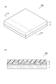
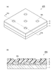
- FIGS. 1 to 5 are schematic views (schematic perspective view and schematic end view) showing an embodiment of a manufacturing process of a semiconductor element having a multilayer wiring structure.
- FIGS. 1 to 5 (a) is a schematic perspective view, and (b) is a schematic end view showing the Ib-Ib to Vb-Vb end faces in (a), respectively.
- the structure 100 shown in FIG. 1 is prepared.
- the structure 100 has a semiconductor substrate 1 such as a Si substrate having a circuit element, a protective film 2 such as a silicon oxide film having a predetermined pattern in which the circuit element is exposed and covering the semiconductor substrate 1, and an exposed circuit element.
- the first conductor layer 3 formed above and the interlayer insulating layer 4 made of a polyimide resin or the like formed on the protective film 2 and the first conductor layer 3 by a spin coating method or the like are provided.
- the structure 200 shown in FIG. 2 is obtained by forming the photosensitive resin layer 5 having the window portion 6A on the interlayer insulating layer 4.
- the photosensitive resin layer 5 is formed by applying, for example, a photosensitive resin such as a rubber chloride type, a phenol novolac type, a polyhydroxystyrene type, or a polyacrylic acid ester type by a spin coating method.
- the window portion 6A is formed by a known photographic engraving technique so that the interlayer insulating layer 4 of a predetermined portion is exposed.
- the photosensitive resin layer 5 is removed to obtain the structure 300 shown in FIG.
- a dry etching means using a gas such as oxygen or carbon tetrafluoride can be used for etching the interlayer insulating layer 4.
- the photosensitive resin layer 5 is removed using an etching solution that corrodes only the photosensitive resin layer 5 without corroding the first conductor layer 3 exposed from the window portion 6B.
- the second conductor layer 7 is formed in the portion corresponding to the window portion 6B to obtain the structure 400 shown in FIG.
- a known photographic engraving technique can be used to form the second conductor layer 7.
- the second conductor layer 7 and the first conductor layer 3 are electrically connected.
- the surface protective layer 8 is formed on the interlayer insulating layer 4 and the second conductor layer 7, and the semiconductor element 500 shown in FIG. 5 is obtained.
- the surface protective layer 8 is formed as follows. First, the above-mentioned photosensitive resin composition is applied onto the interlayer insulating layer 4 and the second conductor layer 7 by a spin coating method, and dried to form a resin film. Next, after irradiating a predetermined portion with light through a mask on which a pattern corresponding to the window portion 6C is drawn, the exposed resin film is developed with an alkaline aqueous solution to form a pattern resin film. After that, the pattern resin film is cured by heating to form a pattern cured film used as the surface protective layer 8.
- the surface protective layer 8 protects the first conductor layer 3 and the second conductor layer 7 from external stress, ⁇ rays, and the like, and the semiconductor element 500 using the surface protective layer 8 of the present embodiment is reliable. Excellent in sex.
- a method for manufacturing a semiconductor element having a two-layer wiring structure is shown.
- the above steps are repeated to form each layer.
- not only the surface protective layer 8 but also the interlayer insulating layer 4 can be formed by using the photosensitive resin composition of the present embodiment.
- the electronic device of the present embodiment is not limited to the one having a surface protective layer, a cover coat layer or an interlayer insulating layer formed by using the above-mentioned photosensitive resin composition, and can have various structures.
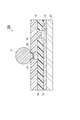
- FIGS. 6 and 7 are schematic cross-sectional views showing an embodiment of a semiconductor device. More specifically, it is a schematic cross-sectional view showing one embodiment of a semiconductor element having a rewiring structure. Since the photosensitive resin composition of the present embodiment is also excellent in stress relaxation property, adhesiveness, etc., it can be used in a semiconductor device having a rewiring structure shown in FIGS. 6 and 7 which has been recently developed.
- the semiconductor element 600 shown in FIG. 6 has an Al having a pattern including a silicon substrate 23, an interlayer insulating layer 11 provided on one surface side of the silicon substrate 23, and a pad portion 15 formed on the interlayer insulating layer 11.
- the wiring layer 12, the insulating layer 13 (for example, P—SiN layer) and the surface protective layer 14 sequentially laminated on the interlayer insulating layer 11 and the Al wiring layer 12 while forming an opening on the pad portion 15, and the surface protection.
- the island-shaped core 18 arranged in the vicinity of the opening on the layer 14 is in contact with the pad portion 15 in the opening of the insulating layer 13 and the surface protection layer 14, and is in contact with the surface of the core 18 opposite to the surface protection layer 14.
- a rewiring layer 16 extending over the surface protective layer 14 is provided. Further, the semiconductor element 600 is formed by covering the surface protection layer 14, the core 18, and the rewiring layer 16, and has a cover coat layer 19 and a cover coat in which an opening is formed in a portion of the rewiring layer 16 on the core 18.
- a conductive ball 17 connected to the rewiring layer 16 with a barrier metal 20 sandwiched between the openings of the layer 19, a collar 21 for holding the conductive ball, and a cover coat layer 19 around the conductive ball 17 are provided.
- the underfill 22 is provided.
- the conductive ball 17 is used as an external connection terminal and is formed of solder, gold, or the like.
- the underfill 22 is provided to relieve stress when mounting the semiconductor element 600.
- an Al wiring layer (not shown) and a pad portion 15 of the Al wiring layer are formed on the silicon substrate 23, and an insulating layer 13 is formed on the pad portion 15 of the Al wiring layer.
- the surface protective layer 14 is formed.
- a rewiring layer 16 is formed on the pad portion 15, and the rewiring layer 16 extends to the upper part of the connecting portion 24 with the conductive ball 17. Further, a cover coat layer 19 is formed on the surface protective layer 14. The rewiring layer 16 is connected to the conductive ball 17 via the barrier metal 20.
- the photosensitive resin composition is a material for forming not only the interlayer insulating layer 11 and the surface protective layer 14, but also the cover coat layer 19, the core 18, the collar 21, the underfill 22, and the like. Can be used as.
- the pattern cured film using the photosensitive resin composition of the present embodiment has excellent adhesion to metal layers such as Al wiring layer 12 and rewiring layer 16, and a sealing agent, and has a high stress relaxation effect.
- Semiconductor devices in which the pattern curing film is used for the interlayer insulating layer 11, the surface protective layer 14, the cover coat layer 19, the core 18, the collar 21 such as solder, the underfill 22 used in flip chips, etc. are extremely reliable. It becomes a thing.
- the photosensitive resin composition of the present embodiment is preferably used for the interlayer insulating layer 11, the surface protective layer 14 and / or the cover coat layer 19 of the semiconductor element having the rewiring layer 16 in FIGS. 6 and 7.
- the film thickness of the interlayer insulating layer 11, the surface protective layer 14, and the cover coat layer 19 may be 3 to 20 ⁇ m or 5 to 15 ⁇ m.
- the electronic device of this embodiment has the semiconductor element of this embodiment.
- the electronic device includes the above-mentioned semiconductor elements, and examples thereof include mobile phones, smartphones, tablet terminals, personal computers, and hard disk suspensions. Since the pattern cured film formed by the photosensitive resin composition of the present embodiment has excellent adhesion to copper, it is possible to provide a semiconductor element and an electronic device having excellent reliability.
- [(A) component] A1 100 parts by mass of p-tert-butoxystyrene and styrene (molar ratio 80:20) are dissolved in 150 parts by mass of propylene glycol monomethyl ether and then kept at 70 ° C. under a nitrogen atmosphere to azobisisobutyro. 4 parts by mass of nitrile was added, and polymerization was carried out for 10 hours while stirring at a stirring rotation speed of about 160 rpm. Then, sulfuric acid was added to the polymerization solution to maintain the reaction temperature at 90 ° C. for 10 hours to deprotect the tert-butoxy group and convert it into a hydroxy group.
- a homopolymer A2 of p-hydroxystyrene was obtained in the same manner as in the synthesis of A1 except that 100 parts by mass of p-tert-butoxystyrene was dissolved in 150 parts by mass of propylene glycol monomethyl ether.
- the Mw of A2 was 10,000.
- THF Tetrahydrofuran
- B1 Bisallyl nadiimide (manufactured by Maruzen Petrochemical Co., Ltd., trade name "BANI-X")
- B2 Bisallyl nadiimide (manufactured by Maruzen Petrochemical Co., Ltd., trade name "BANI-M”)
- C1 A compound in which R 1 to R 6 of the formula (7) are all methyl groups (hexakis (methoxymethyl) melamine, manufactured by Sanwa Chemical Co., Ltd., trade name "Nicarac MW-30HM”).
- C2 A compound in which R 1a to R 6a of the formula (8) are all methyl groups (manufactured by Honshu Chemical Industry Co., Ltd., trade name "HMOM-TPPA”).
- D1 1,1-bis (4-hydroxyphenyl) -1- [4- ⁇ 1- (4-hydroxyphenyl) -1-methylethyl ⁇ phenyl] 1-naphthoquinone-2-diazide-5-sulfonic acid of ethane Ester (esterification rate: about 90%, manufactured by Daito Kemix Co., Ltd., trade name "PA28”)
- LA 2.2 g, acrylic acid (AA) 3.9 g, hydroxybutyl acrylate (HBA) 2.6 g and 1,2,2,6,6-pentamethylpiperidin-4-ylmethacrylate (trade name: FA-) 1.7 g of 711MM (manufactured by Hitachi Kasei Co., Ltd.) and 0.29 g of azobisisobutyronitrile were added.
- Nitrogen gas was added at a flow rate of 400 mL / min while stirring at room temperature at a stirring speed of about 160 rpm. It was allowed to flow for 1 minute to remove dissolved oxygen. After that, the inflow of nitrogen gas was stopped, the flask was sealed, and the temperature was raised to 65 ° C.
- F1 Etherdiamine 4000 (manufactured by BASF) (0.02 mol), 1,12-diaminododecane (0.08 mol) and N in a 500 mL four-necked flask equipped with a thermometer, a stirrer and a calcium chloride tube.
- -Methyl-2-pyrrolidone 150 g was added and stirred at 60 ° C. to obtain a uniform diamine solution.
- 2,2-Bis [4- (3,4-dicarboxyphenoxy) phenyl] propane dianhydride (0.1 mol) was added little by little to the diamine solution, and the mixture was reacted at 60 ° C. for 1 hour.
- reaction solution was heated at 170 ° C. while blowing nitrogen gas, and water was azeotropically removed with a part of the solvent to obtain a solution of the polyimide resin F1.
- F2 4,4'-Bismaleimide diphenylmethane (manufactured by Daiwa Kasei Kogyo Co., Ltd.)
- Examples 1 to 9 After mixing the components (A) to (E) in the blending amount (parts by mass) shown in Table 1, 120 parts by mass of ethyl lactate as a solvent, and 1 part by mass of KBM-403 (manufactured by Shin-Etsu Chemical Industry Co., Ltd.) as a coupling agent. , 0.2 ⁇ m pore Teflon (registered trademark) filter was used for pressure filtration to prepare a photosensitive resin composition.
- the photosensitive resin composition is spin-coated on a copper substrate (a substrate in which TiN is sputtered on a silicon substrate and then copper is sputtered on the TiN) and heated at 120 ° C. for 4 minutes to obtain a film thickness of 11.
- a resin film of ⁇ 13 ⁇ m was formed.
- a vertical diffusion furnace manufactured by Koyo Thermo System Co., Ltd., trade name " ⁇ -TF"
- heat treatment curing
- the adhesion of the cured film to copper was evaluated by the following cross-cut test.
- A There is no peeling at the intersection of the cuts and the square at a glance, and the area of the defect is less than 1% of the total square area.
- B There is a slight peeling at the intersection of the cuts, there is no peeling at a glance of the square, and the area of the defective portion is less than 5% of the total square area.
- C There is peeling at both sides and intersections of the cut, and the area of the defect is 5 to 50% of the total square area.
- D The width of peeling due to a cut is large, and the area of the defect is larger than 50% of the total square area.
- the copper substrate on which the cured film was formed by the above method was heated on a hot plate at 260 ° C. for 3 minutes 5 times, and then using ETAC WINTECH NT1010 (manufactured by Kusumoto Kasei Co., Ltd.) at -65 ° C./ A 100-cycle thermal shock test was performed with 30 minutes to 150 ° C./30 minutes as one cycle. After the heat treatment test, a cross-cut test was performed to evaluate the adhesion of the cured film to copper.
- the photosensitive resin composition was spin-coated on a silicon substrate and heated at 120 ° C. for 4 minutes to form a resin film having a film thickness of about 12 to 14 ⁇ m.
- a proximity exposure machine manufactured by Canon Inc., trade name "PLA-600FA"
- the resin film was exposed to the resin film at 600 mJ / cm 2 at all wavelengths through a mask.
- development was carried out using a 2.38% TMAH aqueous solution to obtain a pattern resin film having a width of 10 mm.
- a silicon substrate on which a pattern resin film is formed is used in a vertical diffusion furnace (manufactured by Koyo Thermo System Co., Ltd., trade name " ⁇ -TF") in nitrogen at a temperature of 230 ° C. (heating time: 1.5 hours) for 2 hours. Heat treatment was performed to obtain a cured film having a film thickness of about 10 ⁇ m.
- the cured film was peeled off from the silicon substrate, and the elongation at break of the cured film was measured using the trade name "Autograph AGS-H100N" manufactured by Shimadzu Corporation.
- the width of the sample was 10 mm, the film thickness was about 10 ⁇ m, and the distance between the chucks was 20 mm.
- the tensile speed was 5 mm / min, and the measurement temperature was about room temperature (20 ° C to 25 ° C).
- the average from the top three points of the measured values of the five test pieces obtained from the cured film obtained under the same conditions was defined as the elongation at break. It is preferable that the cured film has a large breaking elongation.
- the silicon substrate on which the cured film was formed by the above method was heat-treated by repeating heating on a hot plate at 260 ° C. for 3 minutes 5 times, and then the cured film was peeled off from the silicon substrate.
- the elongation at break of the cured film was measured in the same manner as above.
- the breaking elongation of the dura mater after the heat treatment is preferably large, and the difference from the breaking elongation of the cured film before the heat treatment is preferably small.
- residual stress The residual stress of the silicon substrate on which the cured film was formed by the same method as the measurement of the elongation at break was measured using a stress measuring device (manufactured by KLA Tencor Co., Ltd., FLX-2320 type). The smaller the residual stress, the better.
- Tg The cured film was peeled off from the silicon substrate on which the cured film was formed in the same manner as in the measurement of elongation at break, and the Tg of the cured film was measured with a dynamic viscoelasticity measuring device (manufactured by TA Instruments, RSA-G2). At the time of measurement, the width of the sample was 10 mm, the film thickness was about 10 ⁇ m, and the distance between the chucks was 20 mm. The heating rate was 5 ° C./min.
- the Tg of the cured film is preferably high.
- the photosensitive resin composition was spin-coated on a silicon substrate and heated at 120 ° C. for 4 minutes to form a resin film having a film thickness of 11 to 13 ⁇ m. Then, using an i-line stepper (manufactured by Canon Inc., trade name "FPA-3000iW"), an i-line (365 nm) was formed on a resin film through a mask having a square hole pattern from 1 ⁇ m ⁇ 1 ⁇ m to 100 ⁇ m ⁇ 100 ⁇ m. On the other hand, reduced projection exposure was performed. The exposure amount was 600 mJ / cm 2 .
- the exposed resin film was developed with a 2.38% aqueous solution of TMAH and rinsed with water to obtain a patterned resin film.
- the openness of a 100 ⁇ m ⁇ 100 ⁇ m square hole pattern was evaluated according to the following criteria. A: The pattern is open, and there is no pattern peeling or undissolved opening. B: The pattern is open, but peeling of the pattern or undissolved residue can be confirmed in the opening. C: The pattern itself cannot be formed.
- the above pattern resin film is heat-treated in nitrogen at a temperature of 230 ° C. (heating time 1.5 hours) for 2 hours using a vertical diffusion furnace (manufactured by Koyo Thermo System Co., Ltd., trade name " ⁇ -TF") to obtain a pattern.
- the resolution of the cured film was evaluated.
- the minimum size of the square hole pattern from 1 ⁇ m ⁇ 1 ⁇ m to 100 ⁇ m ⁇ 100 ⁇ m was used as an index of microfabrication. The smaller the pattern size, the better the resolution and the finer the processing becomes.
- the photosensitive resin composition of the example had good adhesion and elongation at break before and after the heat treatment, and was also excellent in microfabrication.
- the resin composition of Comparative Example 1 had reduced adhesion and elongation at break after the heat treatment.
- the resin compositions of Comparative Examples 2 and 3 were cloudy, the cured film could not be evaluated.
Landscapes
- Physics & Mathematics (AREA)
- General Physics & Mathematics (AREA)
- Materials For Photolithography (AREA)
- Exposure And Positioning Against Photoresist Photosensitive Materials (AREA)
Abstract
Description
一実施形態に係る感光性樹脂組成物は、アルカリ可溶性樹脂(以下、「(A)成分」という場合がある。)と、式(1)で表されるナジイミド系化合物(以下、「(B)成分」という場合がある。)と、熱架橋剤(以下、「(C)成分」という場合がある。)と、光により酸を発生する化合物(以下、「(D)成分」という場合がある。)と、を含有する。感光性樹脂組成物は、ポジ型感光性樹脂組成物として好適に用いることができる。以下、ポジ感光性樹脂組成物の形態について、詳細に説明する。
本明細書において、アルカリ可溶性樹脂は、アルカリ水溶液(現像液)に対して可溶である樹脂を意味する。なお、アルカリ水溶液とは、テトラメチルアンモニウムヒドロキシド(TMAH)水溶液、金属水酸化物水溶液、有機アミン水溶液等のアルカリ性の溶液である。一般には、濃度が2.38質量%のTMAH水溶液が現像に用いられる。(A)成分がアルカリ現像液に可溶であることは、例えば、以下のようにして確認することができる。


(B)成分であるナジイミド化合物は、下記式(1)で表される構造単位を有することで、熱安定性の向上効果が得られ、(A)成分と相溶性が高い。

(C)成分である架橋剤は、パターン形成後の樹脂膜を加熱して硬化する際に、(A)成分と反応して橋架け構造(架橋構造)を形成し得る基を有する化合物である。これにより、樹脂膜の脆さ及び樹脂膜の溶融を防ぐことができる。(C)成分としては、例えば、2以上のアルコキシメチル基を有する化合物及び2以上のエポキシ基を有する化合物が挙げられる。

(D)成分である光によって(光を受けることにより)酸を生成する化合物は、感光性樹脂組成物において感光剤として機能する。(D)成分は、光照射を受けて酸を生成させ、光照射を受けた部分のアルカリ水溶液への可溶性を増大させる機能を有する。(D)成分としては、一般に光酸発生剤と称される化合物を用いることができる。(D)成分の具体例としては、o-キノンジアジド化合物、アリールジアゾニウム塩、ジアリールヨードニウム塩及びトリアリールスルホニウム塩が挙げられる。(D)成分は、これらの化合物のうちの1種のみを含んでもよく、2種以上を含んでもよい。これらの中で、感度が高いことから、(D)成分は、o-キノンジアジド化合物であってよい。
本実施形態の感光性樹脂組成物は、パターン硬化膜の柔軟性を向上する観点から、エラストマ(以下、「(E)成分」という場合がある。)を更に含有してもよい。




本実施形態の感光性樹脂組成物は、溶剤を含有することにより、基板上への塗布を容易にし、均一な厚さの樹脂膜を形成できるという効果を奏する。溶剤としては、例えば、γ-ブチロラクトン、乳酸エチル、プロピレングリコールモノメチルエーテルアセテート、酢酸ベンジル、n-ブチルアセテート、エトキシエチルプロピオナート、3-メチルメトキシプロピオナート、N-メチル-2-ピロリドン、N,N-ジメチルホルムアミド、N,N-ジメチルアセトアミド、ジメチルスルホキシド、ヘキサメチルホスホリルアミド、テトラメチレンスルホン、ジエチルケトン、ジイソブチルケトン、メチルアミルケトン、シクロヘキサノン、プロピレングリコールモノメチルエーテル、プロピレングリコールモノプロピルエーテル、プロピレングリコールモノブチルエーテル及びジプロピレングリコールモノメチルエーテルが挙げられる。これらの溶剤は1種を単独で又は2種以上を組み合わせて用いることができる。これらの中でも、各成分の溶解性と樹脂膜の均一性との点から、溶剤として、乳酸エチル又はプロピレングリコールモノメチルエーテルアセテートを用いることが好ましい。
加熱により酸を生成する化合物を用いることにより、パターン樹脂膜を加熱する際に酸を発生させることが可能となり、(A)成分と(C)成分との反応、すなわち熱架橋反応が促進され、パターン硬化膜の耐熱性が向上する。また、加熱により酸を生成する化合物は光照射によっても酸を発生するため、露光部のアルカリ水溶液への溶解性が増大する。よって、未露光部と露光部とのアルカリ水溶液に対する溶解性の差がさらに大きくなり、解像性がより向上する。
溶解促進剤を感光性樹脂組成物に配合することによって、樹脂膜をアルカリ水溶液で現像する際の露光部の溶解速度を増加させ、感度及び解像性を向上させることができる。溶解促進剤としては従来公知の化合物を用いることができる。溶解促進剤の具体例としては、カルボキシル基、スルホン酸又はスルホンアミド基を有する化合物が挙げられる。
溶解阻害剤を(A)成分のアルカリ水溶液に対する溶解性を阻害する化合物であり、残膜厚、現像時間及びコントラストをコントロールするために用いられる。溶解阻害剤としては、例えば、ジフェニルヨードニウムニトラート、ビス(p-tert-ブチルフェニル)ヨードニウムニトラート、ジフェニルヨードニウムブロミド、ジフェニルヨードニウムクロリド及びジフェニルヨードニウムヨージドが挙げられる。溶解阻害剤を用いる場合の含有量は、感度と現像時間の許容幅の点から、(A)成分100質量部に対して0.01~20質量部が好ましく、0.01~15質量部がより好ましく、0.05~10質量部が更に好ましい。
カップリング剤を感光性樹脂組成物に配合することによって、形成されるパターン硬化膜の基板との接着性をより高めることができる。カップリング剤としては、例えば、有機シラン化合物及びアルミキレート化合物が挙げられる。有機シラン化合物としては、例えば、KBM-403、KBM-803及びKBM-903(信越化学工業株式会社製、商品名)が挙げられる。カップリング剤を用いる場合の含有量は、(A)成分100質量部に対して、0.1~20質量部が好ましく、0.5~10質量部がより好ましい。
界面活性剤又はレベリング剤を感光性樹脂組成物に配合することによって、塗布性をより向上することができる。具体的には、例えば、界面活性剤又はレベリング剤を含有することで、ストリエーション(膜厚のムラ)をより防いだり、現像性をより向上させたりすることができる。界面活性剤又はレベリング剤としては、例えば、ポリオキシエチレンラウリルエーテル、ポリオキシエチレンステアリルエーテル、ポリオキシエチレンオレイルエーテル及びポリオキシエチレンオクチルフェノールエーテルが挙げられる。市販品としては、例えば、メガファックF-171、F-565、RS-78(DIC株式会社製、商品名)が挙げられる。
一実施形態のパターン硬化膜は、パターンを有し、パターンが上述の感光性樹脂組成物からなる樹脂膜の硬化物を含む。パターン硬化膜は、上述の感光性樹脂組成物を加熱することによって得られる。以下、パターン硬化膜の製造方法について説明する。
まず、本実施形態の感光性樹脂組成物を基板上に塗布し乾燥して樹脂膜を形成する。この工程では、ガラス基板、半導体、金属酸化物絶縁体(例えば、TiO2、SiO2)、窒化ケイ素等の基板上に、本実施形態の感光性樹脂組成物を、スピンナー等を用いて回転塗布し、塗膜を形成する。塗膜の厚さに特に制限されないが、0.1~40μmであってよい。この塗膜が形成された基板をホットプレート、オーブン等を用いて乾燥する。乾燥温度及び乾燥時間に特に制限はないが、80~140℃で1~7分間であってよい。これによって、支持基板上に樹脂膜が形成される。樹脂膜の厚さに特に制限はないが、0.1~40μmであってよい。
次に、露光工程では、基板上に形成した樹脂膜に、マスクを介して紫外線、可視光線、放射線等の活性光線を照射する。本実施形態の感光性樹脂組成物において、(A)成分はg、h、i線に対する透明性が高いので、g、h、i線のいずれか又は全てを照射に用いることができる。
現像工程では、露光工程後の樹脂膜の露光部を現像液で除去することによって、樹脂膜がパターン化され、パターン樹脂膜が得られる。現像液としては、例えば、炭酸ナトリウム、水酸化ナトリウム、水酸化カリウム、ケイ酸ナトリウム、アンモニア、エチルアミン、ジエチルアミン、トリエチルアミン、トリエタノールアミン、水酸化テトラメチルアンモニウム(TMAH)等のアルカリ水溶液が好適に用いられる。これらの水溶液の塩基濃度は、0.1~10質量%であってよい。上記現像液にアルコール類又は界面活性剤を添加して使用することもできる。これらはそれぞれ、現像液100質量部に対して、0.01~10質量部又は0.1~5質量部の範囲で配合してよい。現像液を用いて現像を行う場合は、例えば、シャワー現像、スプレー現像、浸漬現像、パドル現像等の方法によって、現像液を樹脂膜上に配し、18~40℃の条件下、30~360秒間放置する。放置後、水洗しスピン乾燥を行うことによってパターン樹脂膜を洗浄する。
次いで、加熱処理工程では、パターン樹脂膜を加熱処理することによって、パターン硬化膜を形成することができる。加熱処理工程における加熱温度は、半導体装置に対する熱によるダメージを充分に防止する点から、300℃以下、280℃以下、又は260℃以下であってよい。
本実施形態のパターン硬化膜は、半導体素子の層間絶縁層又は表面保護層として用いることができる。
一実施形態の半導体素子は、本実施形態の層間絶縁層又は表面保護層を備える。本実施形態の半導体素子は、特に制限されないが、多層配線構造、再配線構造等を有する、メモリ、パッケージ等のことを意味する。
本実施形態の電子デバイスは、本実施形態の半導体素子を有する。電子デバイスとは、上述の半導体素子を含むものであり、例えば、携帯電話、スマートフォン、タブレット型端末、パソコン及びハードディスクサスペンションが挙げられる。本実施形態の感光性樹脂組成物により形成されるパターン硬化膜は銅との密着性に優れているため、信頼性に優れた半導体素子及び電子デバイスを提供することができる。
A1:p-tert-ブトキシスチレン及びスチレン(モル比80:20)100質量部を、プロピレングリコールモノメチルエーテル150質量部に溶解した後、窒素雰囲気下、70℃に保持して、アゾビスイソブチロニトリル4質量部を添加して、約160rpmの攪拌回転数で攪拌しながら、10時間、重合を行った。その後、重合液に硫酸を加えて反応温度を90℃に保持して10時間反応させ、tert-ブトキシ基を脱保護してヒドロキシ基に変換した。反応液に酢酸エチルを加え、水洗を5回繰り返し、酢酸エチル相を分取し、溶剤を除去して、p-ヒドロキシスチレン/スチレンの共重合体A1を得た。A1のMwは10000であった。13C-NMR分析の結果、A1におけるp-ヒドロキシスチレン/スチレンのモル比は80/20であった。
A2:p-tert-ブトキシスチレン100質量部をプロピレングリコールモノメチルエーテル150質量部に溶解させた以外は、A1の合成と同様にして、p-ヒドロキシスチレンの単独重合体A2を得た。A2のMwは10000であった。
検出器:株式会社日立製作所製の「L4000UV」
ポンプ:株式会社日立製作所製の「L6000」
データ処理装置:株式会社島津製作所製C-R4A Chromatopac
カラム:Gelpack GL-S300MDT-5×2本
溶離液:LiBr(0.03mol/L)及びH3PO4(0.06mol/L)を含むテトラヒドロフラン(THF)
流速:1.0mL/分
測定波長:UV270nm
測定試料:試料0.5mgに対して溶媒[THF/DMF=1/1(容積比)]1mLを添加した試料液を用いた。
B1:ビスアリルナジイミド(丸善石油化学株式会社製、商品名「BANI-X」)
B2:ビスアリルナジイミド(丸善石油化学株式会社製、商品名「BANI-M」)
C1:式(7)のR1~R6が全てメチル基である化合物(ヘキサキス(メトキシメチル)メラミン、株式会社三和ケミカル製、商品名「ニカラックMW-30HM」)
C2:式(8)のR1a~R6aが全てメチル基である化合物(本州化学工業株式会社製、商品名「HMOM-TPPA」)
D1:1,1-ビス(4-ヒドロキシフェニル)-1-[4-{1-(4-ヒドロキシフェニル)-1-メチルエチル}フェニル]エタンの1-ナフトキノン-2-ジアジド-5-スルホン酸エステル(エステル化率約90%、ダイトーケミックス株式会社製、商品名「PA28」)
E1:攪拌機、窒素導入管及び温度計を備えた100mLの三口フラスコに、乳酸エチル55gを秤取し、別途に秤取したモノマ(アクリル酸n-ブチル(BA)34.7g、アクリル酸ラウリル(LA)2.2g、アクリル酸(AA)3.9g、アクリル酸ヒドロキシブチル(HBA)2.6g及び1,2,2,6,6-ペンタメチルピペリジン-4-イルメタクリレート(商品名:FA-711MM、日立化成株式会社製)1.7g、並びにアゾビスイソブチロニトリル0.29gを加えた。室温にて約160rpmの攪拌回転数で攪拌しながら、窒素ガスを400mL/分の流量で30分間流し、溶存酸素を除去した。その後、窒素ガスの流入を止め、フラスコを密閉し、恒温水槽にて約25分で65℃まで昇温した。同温度を10時間保持して重合反応を行い、アクリル系エラストマE1を得た。この際の重合率は99%であった。E1のMwは、約22000であった。E1におけるモノマのモル比は下記のとおりである。
BA/LA/AA/HBA/FA711MM=75.5/2.5/15/5/2(mol%)
E2:モノマの配合量を変更した以外は、E1と同様の重合反応を行い、アクリル系エラストマE2を得た。この際の重合率は99%であった。E2のMwは、約15000であった。E2におけるモノマのモル比は下記のとおりである。
BA/LA/AA/HBA/FA711MM=65.0/5.0/20/5/5(mol%)
F1:温度計、攪拌機及び塩化カルシウム管を備えた500mLの四つ口フラスコに、エーテルジアミン4000(BASF社製)(0.02モル)、1,12―ジアミノドデカン(0.08モル)及びN-メチル-2-ピロリドン150gを加え、60℃で攪拌して均一なジアミン溶液を得た。ジアミン溶液に2,2-ビス[4-(3,4-ジカルボキシフェノキシ)フェニル]プロパン二無水物(0.1モル)を少量ずつ添加し、60℃で1時間反応させた。次いで、反応液に窒素ガスを吹き込みながら170℃で加熱し、水を溶剤の一部と共沸除去して、ポリイミド樹脂F1の溶液を得た。
F2:4,4’-ビスマレイミドジフェニルメタン(大和化成工業株式会社製)
表1に示す配合量(質量部)の(A)~(E)成分、溶剤として乳酸エチル120質量部及びカップリング剤としてKBM-403(信越化学工業株式会社製)1質量部を混合した後、0.2μm孔のテフロン(登録商標)フィルターを用いて加圧ろ過して、感光性樹脂組成物を調製した。
表2に示した配合量の(A)、(C)~(F)成分を用いた以外は、実施例と同様にして、感光性樹脂組成物を調製した。
(外観)
感光性樹脂組成物の外観を目視で観察し、透明であれば「A」、若干白濁していれば「B」、酷く白濁していれば「C」と判定した。感光性樹脂組成物の白濁が「A」又は「B」であれば、感光性樹脂組成物を用いて形成したパターン硬化膜を有する半導体装置を製造する際の、基板上に記された位置合わせのための目印が認識できる。
感光性樹脂組成物を、銅基板(シリコン基板上にTiNをスパッタ形成後、更にそのTiN上に銅をスパッタ形成した基板)上にスピンコートして、120℃で4分間加熱し、膜厚11~13μmの樹脂膜を形成した。その後、縦型拡散炉(光洋サーモシステム株式会社製、商品名「μ-TF」)を用い、窒素中、温度230℃(昇温時間1.5時間)で2時間加熱処理(硬化)して、膜厚約10μmの硬化膜を得た。硬化膜の銅に対する密着性を以下のクロスカット試験によって評価した。
A:切り傷の交点、及び正方形の一目一目に剥がれがなく、欠損部の面積が全正方形面積の1%未満である。
B:切り傷の交点にわずかな剥がれがあって、正方形の一目一目に剥がれがなく、欠損部の面積が全正方形面積の5%未満である。
C:切り傷の両側と交点に剥がれがあって、欠損部の面積が全正方形面積の5~50%である。
D:切り傷による剥がれの幅が大きく、欠損部の面積が全正方形面積の50%よりも大きい。
感光性樹脂組成物をシリコン基板上にスピンコートして、120℃で4分間加熱し、膜厚約12~14μmの樹脂膜を形成した。プロキシミティ露光機(キャノン株式会社製、商品名「PLA-600FA」)を用いて、マスクを介して全波長で、600mJ/cm2で樹脂膜に対して露光を行った。露光後、2.38%のTMAH水溶液を用いて現像を行い、10mm幅のパターン樹脂膜を得た。パターン樹脂膜を形成したシリコン基板を縦型拡散炉(光洋サーモシステム株式会社製、商品名「μ-TF」)を用い、窒素中、温度230℃(昇温時間1.5時間)で2時間加熱処理し、膜厚約10μmの硬化膜を得た。
破断伸びの測定と同様の方法で硬化膜を形成したシリコン基板の残留応力を応力測定装置(ケーエルエー・テンコール株式会社製、FLX-2320型)を用いて測定した。残留応力は、数値が小さいほどよい。
破断伸びの測定と同様の方法で硬化膜を形成したシリコン基板から硬化膜を剥離し、硬化膜のTgを動的粘弾性測定装置(TA Instruments製、RSA-G2)で測定した。測定の際、試料の幅は10mm、膜厚は約10μmであり、チャック間は20mmとした。昇温速度は5℃/分であった。硬化膜のTgは高いことが好ましい。
感光性樹脂組成物をシリコン基板上にスピンコートして、120℃で4分間加熱し、膜厚11~13μmの樹脂膜を形成した。次いで、i線ステッパー(キャノン株式会社製、商品名「FPA-3000iW」)を用いて、1μm×1μmから100μm×100μmまでの正方形ホールパターンを有するマスクを介してi線(365nm)で樹脂膜に対して縮小投影露光した。露光量は、600mJ/cm2で行った。露光後の樹脂膜を2.38%のTMAH水溶液を用いて現像し、水でリンスしてパターン樹脂膜を得た。100μm×100μmの正方形ホールパターンの開口性を下記基準で評価した。
A:パターンが開口しており、パターン剥がれ及び開口部の溶け残りがない。
B:パターンが開口しているが、パターンの剥がれ又は開口部に溶け残りが確認できる。
C:パターン自体が形成できない。
上記パターン樹脂膜を縦型拡散炉(光洋サーモシステム社製、商品名「μ-TF」)を用い、窒素中、温度230℃(昇温時間1.5時間)で2時間加熱処理し、パターン硬化膜の解像度を評価した。1μm×1μmから100μm×100μmまでの正方形ホールパターンで開口している最小サイズを微細加工性の指標とした。パターンサイズが小さい程、解像性に優れ微細加工が可能となる。


Claims (9)
- アルカリ可溶性樹脂と、下記式(1)で表されるナジイミド化合物と、
熱架橋剤と、光によって酸を生成する化合物と、を含有する感光性樹脂組成物。

- 前記ナジイミド化合物が、下記式(2)で表される化合物である、請求項1に記載の感光性樹脂組成物。
- 前記光により酸を生成する化合物が、o-キノンジアジド化合物である、請求項1又は2に記載の感光性樹脂組成物。
- エラストマを更に含有する、請求項1~3のいずれか一項に記載の感光性樹脂組成物。
- 前記エラストマがアクリル系エラストマを含む、請求項4に記載の感光性樹脂組成物。
- パターンを有し、前記パターンが請求項1~5のいずれか一項に記載の感光性樹脂組成物からなる樹脂膜の硬化物を含む、パターン硬化膜。
- 請求項1~5のいずれか一項に記載の感光性樹脂組成物を基板の一部又は全部に塗布して樹脂膜を形成する工程と、
前記樹脂膜の一部又は全部を露光する工程と、
露光後の前記樹脂膜をアルカリ水溶液によって現像してパターン樹脂膜を形成する工程と、
前記パターン樹脂膜を加熱する工程と、
を備える、パターン硬化膜の製造方法。 - 請求項6に記載のパターン硬化膜を層間絶縁層又は表面保護層として備える、半導体素子。
- 請求項8に記載の半導体素子を備える、電子デバイス。
Priority Applications (2)
| Application Number | Priority Date | Filing Date | Title |
|---|---|---|---|
| JP2021504683A JP7287453B2 (ja) | 2019-03-12 | 2019-03-12 | 感光性樹脂組成物、パターン硬化膜及びその製造方法、半導体素子並びに電子デバイス |
| PCT/JP2019/010057 WO2020183617A1 (ja) | 2019-03-12 | 2019-03-12 | 感光性樹脂組成物、パターン硬化膜及びその製造方法、半導体素子並びに電子デバイス |
Applications Claiming Priority (1)
| Application Number | Priority Date | Filing Date | Title |
|---|---|---|---|
| PCT/JP2019/010057 WO2020183617A1 (ja) | 2019-03-12 | 2019-03-12 | 感光性樹脂組成物、パターン硬化膜及びその製造方法、半導体素子並びに電子デバイス |
Publications (1)
| Publication Number | Publication Date |
|---|---|
| WO2020183617A1 true WO2020183617A1 (ja) | 2020-09-17 |
Family
ID=72427406
Family Applications (1)
| Application Number | Title | Priority Date | Filing Date |
|---|---|---|---|
| PCT/JP2019/010057 Ceased WO2020183617A1 (ja) | 2019-03-12 | 2019-03-12 | 感光性樹脂組成物、パターン硬化膜及びその製造方法、半導体素子並びに電子デバイス |
Country Status (2)
| Country | Link |
|---|---|
| JP (1) | JP7287453B2 (ja) |
| WO (1) | WO2020183617A1 (ja) |
Citations (5)
| Publication number | Priority date | Publication date | Assignee | Title |
|---|---|---|---|---|
| JP2004062142A (ja) * | 2002-03-28 | 2004-02-26 | Hitachi Chemical Dupont Microsystems Ltd | ポジ型感光性樹脂組成物、パターンの製造方法及び電子部品 |
| WO2008123053A1 (ja) * | 2007-03-30 | 2008-10-16 | Toray Industries, Inc. | ポジ型感光性樹脂組成物 |
| WO2009145153A1 (ja) * | 2008-05-29 | 2009-12-03 | 旭化成イーマテリアルズ株式会社 | 感光性樹脂組成物 |
| JP2011013644A (ja) * | 2009-07-06 | 2011-01-20 | Asahi Kasei E-Materials Corp | 感光性樹脂組成物 |
| JP2017187752A (ja) * | 2016-03-31 | 2017-10-12 | 東京応化工業株式会社 | 層間絶縁膜形成用組成物、層間絶縁膜及び層間絶縁膜パターンの形成方法、並びにデバイス |
-
2019
- 2019-03-12 WO PCT/JP2019/010057 patent/WO2020183617A1/ja not_active Ceased
- 2019-03-12 JP JP2021504683A patent/JP7287453B2/ja active Active
Patent Citations (5)
| Publication number | Priority date | Publication date | Assignee | Title |
|---|---|---|---|---|
| JP2004062142A (ja) * | 2002-03-28 | 2004-02-26 | Hitachi Chemical Dupont Microsystems Ltd | ポジ型感光性樹脂組成物、パターンの製造方法及び電子部品 |
| WO2008123053A1 (ja) * | 2007-03-30 | 2008-10-16 | Toray Industries, Inc. | ポジ型感光性樹脂組成物 |
| WO2009145153A1 (ja) * | 2008-05-29 | 2009-12-03 | 旭化成イーマテリアルズ株式会社 | 感光性樹脂組成物 |
| JP2011013644A (ja) * | 2009-07-06 | 2011-01-20 | Asahi Kasei E-Materials Corp | 感光性樹脂組成物 |
| JP2017187752A (ja) * | 2016-03-31 | 2017-10-12 | 東京応化工業株式会社 | 層間絶縁膜形成用組成物、層間絶縁膜及び層間絶縁膜パターンの形成方法、並びにデバイス |
Also Published As
| Publication number | Publication date |
|---|---|
| JPWO2020183617A1 (ja) | 2020-09-17 |
| JP7287453B2 (ja) | 2023-06-06 |
Similar Documents
| Publication | Publication Date | Title |
|---|---|---|
| TWI461851B (zh) | 正型感光性樹脂組成物、光阻圖案的製造方法、半導體裝置以及電子元件 | |
| US10175577B2 (en) | Photosensitive resin composition, method for manufacturing patterned cured film, and electronic component | |
| KR101379057B1 (ko) | 포지티브형 감광성 수지 조성물, 레지스트 패턴의 제조 방법 및 전자 부품 | |
| TWI442184B (zh) | 正型感光性樹脂組成物、光阻圖案的製造方法及電子零件 | |
| KR102875401B1 (ko) | 감광성 수지 조성물, 패턴 경화막의 제조 방법, 패턴 경화막, 및 반도체 소자 | |
| TWI472875B (zh) | 感光性樹脂組成物、圖案硬化膜的製造方法以及電子零件 | |
| TW201615696A (zh) | 樹脂及感光性樹脂組成物 | |
| KR101290041B1 (ko) | 포지티브형 감광성 절연 수지 조성물, 그 경화물 및 전자부품 | |
| JP2012226044A (ja) | ポジ型感光性樹脂組成物、レジストパターンの製造方法、半導体装置及び電子デバイス | |
| JP5679095B2 (ja) | 感光性樹脂組成物、パターン硬化膜の製造方法、半導体素子及び電子デバイス | |
| JP4765951B2 (ja) | 絶縁膜を有する大型シリコンウエハおよびその製造方法 | |
| JP2013134346A (ja) | 感光性樹脂組成物、パターン硬化膜の製造方法、半導体装置及び電子部品 | |
| JP7092121B2 (ja) | ポジ型感光性樹脂組成物、ポジ型感光性樹脂用熱架橋剤、パターン硬化膜及びその製造方法、半導体素子、並びに電子デバイス | |
| JP2020158703A (ja) | 樹脂組成物、硬化物、半導体素子及び電子デバイス | |
| JP6513596B2 (ja) | 感光性樹脂組成物、パターン硬化膜の製造方法、半導体装置及び電子部品 | |
| JP7287453B2 (ja) | 感光性樹脂組成物、パターン硬化膜及びその製造方法、半導体素子並びに電子デバイス | |
| JP2013167693A (ja) | 感光性樹脂組成物、パターン硬化膜の製造方法、及び、該パターン硬化膜を有する半導体装置 | |
| JP2018028690A (ja) | 感光性樹脂組成物、パターン硬化膜の製造方法、半導体装置及び電子部品 | |
| JP2022043573A (ja) | 感光性樹脂組成物、パターン硬化膜及びその製造方法、半導体素子、並びに半導体デバイス | |
| WO2025134386A1 (ja) | ポジ型感光性樹脂組成物、絶縁樹脂膜、絶縁樹脂膜を形成する方法、及び半導体装置 | |
| WO2025134385A1 (ja) | ポジ型感光性樹脂組成物、絶縁樹脂膜、絶縁樹脂膜を形成する方法、及び半導体装置 | |
| JP2024002706A (ja) | 感光性樹脂組成物、パターン硬化膜の製造方法、パターン硬化膜、及び半導体素子 |
Legal Events
| Date | Code | Title | Description |
|---|---|---|---|
| 121 | Ep: the epo has been informed by wipo that ep was designated in this application |
Ref document number: 19918857 Country of ref document: EP Kind code of ref document: A1 |
|
| ENP | Entry into the national phase |
Ref document number: 2021504683 Country of ref document: JP Kind code of ref document: A |
|
| NENP | Non-entry into the national phase |
Ref country code: DE |
|
| 32PN | Ep: public notification in the ep bulletin as address of the adressee cannot be established |
Free format text: NOTING OF LOSS OF RIGHTS PURSUANT TO RULE 112(1) EPC (EPO FORM 1205A DATED 10/12/2021) |
|
| 122 | Ep: pct application non-entry in european phase |
Ref document number: 19918857 Country of ref document: EP Kind code of ref document: A1 |