WO2020183589A1 - 表示装置、表示装置の製造方法 - Google Patents
表示装置、表示装置の製造方法 Download PDFInfo
- Publication number
- WO2020183589A1 WO2020183589A1 PCT/JP2019/009804 JP2019009804W WO2020183589A1 WO 2020183589 A1 WO2020183589 A1 WO 2020183589A1 JP 2019009804 W JP2019009804 W JP 2019009804W WO 2020183589 A1 WO2020183589 A1 WO 2020183589A1
- Authority
- WO
- WIPO (PCT)
- Prior art keywords
- layer
- region
- adhesive layer
- display
- area
- Prior art date
- Legal status (The legal status is an assumption and is not a legal conclusion. Google has not performed a legal analysis and makes no representation as to the accuracy of the status listed.)
- Ceased
Links
Images





Classifications
-
- H—ELECTRICITY
- H10—SEMICONDUCTOR DEVICES; ELECTRIC SOLID-STATE DEVICES NOT OTHERWISE PROVIDED FOR
- H10K—ORGANIC ELECTRIC SOLID-STATE DEVICES
- H10K77/00—Constructional details of devices covered by this subclass and not covered by groups H10K10/80, H10K30/80, H10K50/80 or H10K59/80
- H10K77/10—Substrates, e.g. flexible substrates
- H10K77/111—Flexible substrates
-
- G—PHYSICS
- G09—EDUCATION; CRYPTOGRAPHY; DISPLAY; ADVERTISING; SEALS
- G09F—DISPLAYING; ADVERTISING; SIGNS; LABELS OR NAME-PLATES; SEALS
- G09F9/00—Indicating arrangements for variable information in which the information is built-up on a support by selection or combination of individual elements
-
- H—ELECTRICITY
- H10—SEMICONDUCTOR DEVICES; ELECTRIC SOLID-STATE DEVICES NOT OTHERWISE PROVIDED FOR
- H10K—ORGANIC ELECTRIC SOLID-STATE DEVICES
- H10K50/00—Organic light-emitting devices
- H10K50/80—Constructional details
- H10K50/84—Passivation; Containers; Encapsulations
- H10K50/844—Encapsulations
-
- H—ELECTRICITY
- H10—SEMICONDUCTOR DEVICES; ELECTRIC SOLID-STATE DEVICES NOT OTHERWISE PROVIDED FOR
- H10K—ORGANIC ELECTRIC SOLID-STATE DEVICES
- H10K59/00—Integrated devices, or assemblies of multiple devices, comprising at least one organic light-emitting element covered by group H10K50/00
- H10K59/10—OLED displays
- H10K59/12—Active-matrix OLED [AMOLED] displays
-
- H—ELECTRICITY
- H10—SEMICONDUCTOR DEVICES; ELECTRIC SOLID-STATE DEVICES NOT OTHERWISE PROVIDED FOR
- H10K—ORGANIC ELECTRIC SOLID-STATE DEVICES
- H10K71/00—Manufacture or treatment specially adapted for the organic devices covered by this subclass
-
- H—ELECTRICITY
- H10—SEMICONDUCTOR DEVICES; ELECTRIC SOLID-STATE DEVICES NOT OTHERWISE PROVIDED FOR
- H10K—ORGANIC ELECTRIC SOLID-STATE DEVICES
- H10K71/00—Manufacture or treatment specially adapted for the organic devices covered by this subclass
- H10K71/80—Manufacture or treatment specially adapted for the organic devices covered by this subclass using temporary substrates
-
- H—ELECTRICITY
- H10—SEMICONDUCTOR DEVICES; ELECTRIC SOLID-STATE DEVICES NOT OTHERWISE PROVIDED FOR
- H10K—ORGANIC ELECTRIC SOLID-STATE DEVICES
- H10K2102/00—Constructional details relating to the organic devices covered by this subclass
- H10K2102/301—Details of OLEDs
- H10K2102/311—Flexible OLED
-
- H—ELECTRICITY
- H10—SEMICONDUCTOR DEVICES; ELECTRIC SOLID-STATE DEVICES NOT OTHERWISE PROVIDED FOR
- H10K—ORGANIC ELECTRIC SOLID-STATE DEVICES
- H10K59/00—Integrated devices, or assemblies of multiple devices, comprising at least one organic light-emitting element covered by group H10K50/00
- H10K59/10—OLED displays
- H10K59/12—Active-matrix OLED [AMOLED] displays
- H10K59/1201—Manufacture or treatment
-
- H—ELECTRICITY
- H10—SEMICONDUCTOR DEVICES; ELECTRIC SOLID-STATE DEVICES NOT OTHERWISE PROVIDED FOR
- H10K—ORGANIC ELECTRIC SOLID-STATE DEVICES
- H10K59/00—Integrated devices, or assemblies of multiple devices, comprising at least one organic light-emitting element covered by group H10K50/00
- H10K59/40—OLEDs integrated with touch screens
-
- H—ELECTRICITY
- H10—SEMICONDUCTOR DEVICES; ELECTRIC SOLID-STATE DEVICES NOT OTHERWISE PROVIDED FOR
- H10K—ORGANIC ELECTRIC SOLID-STATE DEVICES
- H10K71/00—Manufacture or treatment specially adapted for the organic devices covered by this subclass
- H10K71/40—Thermal treatment, e.g. annealing in the presence of a solvent vapour
-
- Y—GENERAL TAGGING OF NEW TECHNOLOGICAL DEVELOPMENTS; GENERAL TAGGING OF CROSS-SECTIONAL TECHNOLOGIES SPANNING OVER SEVERAL SECTIONS OF THE IPC; TECHNICAL SUBJECTS COVERED BY FORMER USPC CROSS-REFERENCE ART COLLECTIONS [XRACs] AND DIGESTS
- Y02—TECHNOLOGIES OR APPLICATIONS FOR MITIGATION OR ADAPTATION AGAINST CLIMATE CHANGE
- Y02P—CLIMATE CHANGE MITIGATION TECHNOLOGIES IN THE PRODUCTION OR PROCESSING OF GOODS
- Y02P70/00—Climate change mitigation technologies in the production process for final industrial or consumer products
- Y02P70/50—Manufacturing or production processes characterised by the final manufactured product
Definitions
- the present invention has a display area for displaying an image, a frame area surrounding the display area, a terminal area in which the frame area is arranged on the edge of the frame area, and the display area and the terminal.
- the present invention relates to a display device including a bent area bent in a substantially J shape with the area, and a method for manufacturing the display device.
- the frame area is narrowed.
- a configuration is known in which a bent region bent in a substantially J shape is provided between the display region and the terminal region. Then, in order to protect the bent region after bending from stress, the resin is applied to a portion corresponding to the outer circumference of the bent region.
- Patent Document 1 a protective layer for protecting the display portion provided in the display area is provided from the display area to the bent area.
- One aspect of the present invention is to bend the display device into a narrow frame area by a simple configuration and process.
- the display device has a display area for displaying an image and a frame area surrounding the display area, and the frame area is a terminal area arranged on the edge of the frame area and the display.
- a display device including a bent region folded between a region and the terminal region, wherein a substrate arranged in the display region and the frame region, a TFT layer formed on the substrate, and the above-mentioned A light emitting element layer formed in the display region above the TFT layer, a sealing layer formed in the display region so as to cover the light emitting element layer, and a sealing layer formed in the display region above the sealing layer.
- the adhesive layer is provided with a functional layer formed in the display region above the adhesive layer, and a flexible sheet formed on the opposite side of the substrate to the TFT layer, and the TFT layer is at least one layer inorganic.
- the inorganic insulating film includes an insulating film, the inorganic insulating film has a first slit extending the bent region along the edge of the frame region, and the flexible sheet extends the bent region along the edge of the frame region.
- a filling resin layer having two slits and formed so as to fill the first slit is further provided, and the adhesive layer extends from the display area to the frame area to form the first slit and the second slit. It is characterized in that it is formed so as to overlap.
- the method for manufacturing a display device has a display area for displaying an image and a frame area surrounding the display area, and the frame area is a terminal area arranged on the edge of the frame area.
- a method of manufacturing a display device including a bent region folded between the display region and the terminal region, wherein a TFT layer is formed on a substrate arranged in the display region and the frame region.
- a second film in which the adhesive layer and the separator are laminated is attached onto the sealing layer formed in the display region and the TFT layer formed in the display region and the frame region.
- the display device can be bent into a narrow frame region by a simple configuration and process.
- FIG. 5 is a plan view of the display device according to the first embodiment before bending. It is sectional drawing of the said display device. It is a top view of the display device after bending. It is a top view of the display device. It is a flowchart which shows the manufacturing method of the said display device. It is sectional drawing before bending of the modification of the said display device. It is sectional drawing after bending of the modification of the said display device. It is a flowchart which shows the manufacturing method of the modification of the said display device. It is sectional drawing of another modification of the said display device.
- FIG. 5 is a plan view of the display device according to the second embodiment before bending. It is sectional drawing before bending of the said display device.
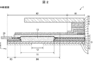
- FIG. 1 is a plan view of the display device 1 according to the first embodiment before bending, and FIG. 2 is a cross-sectional view thereof.
- FIG. 3 is a plan view of the display device 1 after bending, and
- FIG. 4 is a cross-sectional view thereof.
- the display device 1 has a display area R1 for displaying an image and a frame area R2 surrounding the display area R1.
- the frame area R2 includes a terminal area R3 arranged on the edge of the frame area R2, and a bent area R4 bent in a substantially J shape between the display area R1 and the terminal area R3.
- a wiring board (COF, ChipOnFilm) 29 is connected to the terminal area R3.
- the display device 1 has a resin layer 2 (substrate) arranged over the display area R1 and the frame area R2, a TFT layer (thin film transistor layer) 3 formed on the resin layer 2, and a TFT layer 3 on the display device 1.
- the light emitting element layer 4 formed in the display area R1, the sealing layer 5 formed in the display area R1 so as to cover the light emitting element layer 4, and the first formed in the display area R1 above the sealing layer 5.
- the adhesive layer 6 adheresive layer
- the functional layer 7 formed in the display region R1 above the first adhesive layer (OCA, Optical Clear Adhesive) 6, and the resin layer 2 formed on the opposite side of the TFT layer 3.
- a flexible sheet 8 is provided.
- the functional layer 7 includes a touch panel, an antireflection layer (a laminated film of a 1 / 4 ⁇ plate and a linearly polarizing plate), and the like.
- the flexible sheet 8 can be made of a lamination film.
- the resin layer 2 can be made of, for example, polyimide.
- the TFT layer 3 has a base coat layer 20, a semiconductor layer, a gate insulating layer 21, a first metal layer 22, a first inorganic insulating layer 14 (inorganic insulating layer), a second metal layer, and a second inorganic on a substrate.
- the insulating layer 23, the third metal layer, and the flattening layer 24 are formed in this order.
- the base coat layer 20, the gate insulating layer 21, the first inorganic insulating layer 14, and the second inorganic insulating layer 23 are inorganic insulating films such as silicon oxide, silicon nitride, and silicon oxynitride.
- the first metal layer 22, the second metal layer, and the third metal layer are metal layers containing Mo (including molybdenum nitride), Ti, Cu, Al, and the like. It may be a single layer such as Mo, or a laminated film such as Cu / Ti or Ti / Al / Ti in which Ti is formed under Cu.
- the first metal layer 22 constitutes a gate electrode and a scanning signal line.
- the second metal layer constitutes an initialization power line.
- the third metal layer constitutes a data signal line and a high power supply voltage line.
- the above is an example and is not particularly limited.
- the semiconductor layer is made of amorphous silicon, polysilicon, oxide semiconductor, etc.
- the light emitting element layer 4 includes a first electrode, an edge cover that covers the periphery of the first electrode, a light emitting layer, and a second electrode.
- the light emitting layer is composed of an organic EL (ElectroLuminescence), an inorganic EL provided with an inorganic light emitting diode, a QLED (Quantum dot Light Emitting Diode), or the like.
- the sealing layer 5 is formed by providing, for example, an organic resin film between two layers of inorganic insulating films.
- a second adhesive layer (OCA) 25 On the functional layer 7, a second adhesive layer (OCA) 25, a circularly polarizing plate 26, and a third adhesive layer (OCA) 27 are formed in the display region R1 in this order.
- a cover glass 28 is arranged on the third adhesive layer 27 from the display area R1 to the frame area R2.
- the cover glass 28 may be a cover made of a transparent plastic such as polycarbonate or acrylic.
- the first inorganic insulating layer 14 has a first slit 11 extending the bent region R4 along the edge of the frame region R2 in the y direction.
- the first slit 11 is a BCR (Base Coat Rejection) formed by removing the first inorganic insulating layer 14 which is a base coat film.
- the filled resin layer 13 is formed so as to fill the first slit 11.
- the flexible sheet 8 has a second slit 12 extending the bent region R4 along the edge of the frame region R2 in the y direction.
- the first adhesive layer 6 for attaching the functional layer 7 to the sealing layer 5 is formed so as to extend from the display region R1 to the frame region R2 and overlap with the first slit 11 and the second slit 12. There is.
- the second adhesive layer 25 may be extended from the display area R1 to the frame area R2 and formed so as to overlap the first slit 11 and the second slit 12.
- the film thickness of the adhesive layer that protects the TFT layer 3 of the bent region R4 can be increased by stretching the two adhesive layers of the first adhesive layer 6 and the second adhesive layer 25 to the bent region R4. it can.
- the spacer 9 of D1 is arranged.
- the display of the first adhesive layer 10 (adhesive layer) having a thickness D2 for adhering a part of the second slit 12 of the flexible sheet 8 on the display area R1 side and the spacer 9 and the second slit 12 of the flexible sheet 8
- a second adhesive layer 32 having a thickness D3 for adhering the spacer 9 to another part on the opposite side of the region R1 is provided.
- FIG. 5 is a flowchart showing a manufacturing method of the display device 1.
- a TFT layer 3 including a resin layer 2 and a base coat layer 20 is formed on a support substrate (glass substrate) (not shown) (step S1).
- the light emitting element layer 4 is formed on the TFT layer 3 (step S2).
- the sealing layer 5 is formed on the TFT layer 3 so as to cover the light emitting element layer 4 (step S3).
- the first film (first lamination film) is attached to the forming surface side of the sealing layer 5 (step S4).
- the support substrate is peeled from the resin layer 2 (step S5).
- the flexible sheet (second lamination film) 8 is attached to the non-formed surface side of the resin layer 2 (step S6).
- the display element is separated into individual pieces by dividing the resin layer 2 along the direction perpendicular to the resin layer 2, and the terminals are taken out (step S7).
- the flexible sheet 8 of the individualized display element is irradiated with a laser to form the second slit 12 (step S8).
- the wiring board (COF, ChipOnFilm) 29 is mounted on the terminal region R3 of the display element (step S9).
- the first film (first lamination film) is peeled from the sealing layer 5 (step S10).
- the first adhesive layer 6 is attached on the sealing layer 5 (step S11).
- the second film (separator) on the upper layer of the first adhesive layer 6 is peeled off (step S12).
- the functional layer 7 is attached on the first adhesive layer 6 (step S13).
- the functional layer 7 includes an optical compensation function, a touch sensor function, a protection function, and the like.
- the second adhesive layer 25 is attached onto the functional layer 7 (step S14).
- step S15 the circularly polarizing plate 26 is attached onto the second adhesive layer 25 (step S15).
- step S16 the third adhesive layer 27 is attached onto the circularly polarizing plate 26 (step S16).
- step S17 the cover glass 28 is attached onto the third adhesive layer 27 (step S17).
- the bent region R4 of the frame region R2 is bent into a substantially J shape as shown in FIG. 4 (step S18). Then, the first adhesive layer 6 in the bent region R4 is irradiated with ultraviolet rays (UV) 19 along the direction shown in FIG. 4 to cure the first adhesive layer 6 and maintain the bent shape (step S19). The region of the first adhesive layer 6 covered by the cover glass 28 is not cured because the irradiated ultraviolet rays 19 do not reach it.
- UV ultraviolet rays
- FIG. 6 is a cross-sectional view of a modified example of the display device before bending
- FIG. 7 is a cross-sectional view after bending.
- the same components as those described above are designated by the same reference numerals, and the detailed description thereof will not be repeated.
- the first adhesive layer 6A of the display device 1A includes a thick film adhesive portion 16 arranged in the display region R1 and a thin film adhesive portion 17 arranged in the frame region R2 and thinner than the thick film adhesive portion 16. As a result, the first adhesive layer 6A in the bent region R4 becomes thin, so that the display device 1A can be easily bent in the bent region R4.
- the adhesive for adhering the spacer 9 to the flexible sheet 8 is only the first adhesive layer 10, and the second adhesive layer 32 described above in FIG. 4 can be deleted to obtain a single-sided adhesive specification. Therefore, the interval after bending of the flexible sheet 8 is (thickness D1 of the spacer 9) + (thickness D2 of the first adhesive layer 10) + (thickness D3 of the second adhesive layer 32) shown in FIG. The thickness of the spacer 9 is reduced to D1) + (thickness of the first adhesive layer 10 is D2), and the display device can be made thinner.
- FIG. 8 is a flowchart showing a manufacturing method of a modified example of the display device.
- the same components as those described above are designated by the same reference numerals, and the detailed description thereof will not be repeated.
- Steps S1 to S10 shown in FIG. 8 are the same as steps S1 to S10 described in FIG.
- the first adhesive layer 6A is attached onto the sealing layer 5 (step S11A).
- the second film (separator) on the upper layer of the first adhesive layer 6A is peeled off (step S12A).
- the first adhesive layer 6A in the region between the display region R1 and the terminal region R3 is irradiated with a carbon dioxide gas laser to form a thin film adhesive portion 17 (step S43).
- the functional layer 7 is attached on the first adhesive layer 6A (step S13).
- steps S14 to S19 are the same as steps S14 to S19 described with reference to FIG.
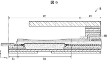
- FIG. 9 is a cross-sectional view of another modified example of the display device.
- the same components as those described above are designated by the same reference numerals, and the detailed description thereof will not be repeated.
- the first adhesive layer 6B is preferably formed to be thinner in the bent region R4 as it approaches the center of the bent region R4. As a result, the first adhesive layer 6B in the bent region R4 becomes thin, so that the display device 1B can be easily bent in the bent region R4.
- FIG. 10 is a plan view of the display device 1C according to the second embodiment before bending, and FIG. 11 is a cross-sectional view thereof.
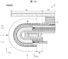
- FIG. 12 is a plan view of the display device 1C after bending, and FIG. 13 is a cross-sectional view thereof.
- the same components as those described above are designated by the same reference numerals, and the detailed description thereof will not be repeated.
- the separator 18 is formed in the frame region R2 above the first adhesive layer 6 so as to overlap the first slit 11 and the second slit 12.
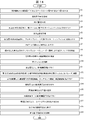
- FIG. 14 is a flowchart showing a manufacturing method of the display device 1C.
- the same components as those described above are designated by the same reference numerals, and the detailed description thereof will not be repeated.
- Steps S1 to S11 shown in FIG. 14 are the same as steps S1 to S11 described with reference to FIG.
- the first adhesive layer 6 has a separator (second film) 18 formed on the upper layer thereof.
- the separator 18 in a region other than the region between the display region R1 and the terminal region R3 on the upper layer of the first adhesive layer 6 is peeled off (step S72).
- the separator 18 remains in the region between the display region R1 and the terminal region R3.
- steps S13 to S19 are the same as steps S13 to S19 described with reference to FIG.
- the first adhesive layer 6 in the bent region R4 is transmitted through the separator 18 and irradiated with ultraviolet rays 19 (UV) to cure the first adhesive layer 6.
- UV ultraviolet rays 19
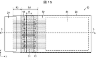
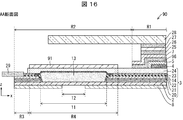
- FIG. 15 is a plan view of the display device 90 according to the comparative example before bending, and FIG. 16 is a cross-sectional view thereof.
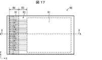
- FIG. 17 is a plan view of the display device 90 after bending, and
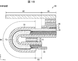
- FIG. 18 is a cross-sectional view thereof.
- the same components as those described above are designated by the same reference numerals, and the detailed description thereof will not be repeated.
- the first adhesive layer 96 is formed in the display region R1 on the flattening layer 24 of the TFT layer 3 so as to cover the sealing layer 5. Then, a resin film 91 for protecting the bent region R4 of the flattening layer 24 is formed in the bent region R4 above the flattening layer 24.
- the resin film 91 needs to be formed by adding a step different from the step of forming the first adhesive layer 96 and the like. Therefore, there arises a problem that man-hours and the number of parts increase.
- the first adhesive layers 6.6A and 6B are stretched from the display area R1 to the frame area R2 and formed so as to overlap the first slit 11 and the second slit 12. Therefore, the first adhesive layers 6.6A and 6B extend from the display region R1 so as to cover the region of the resin film 91 according to the comparative example. Therefore, only the step of forming the first adhesive layer 6 and the like is sufficient, and the need to add a separate step for forming the resin film 91 disappears. Therefore, the display devices 1, 1A, and 1B can be bent to form a narrow frame region by a simple configuration and process.
- the display device of the first aspect has a display area for displaying an image and a frame area surrounding the display area, and the frame area is a terminal area arranged on the edge of the frame area and the display area.
- a display device including a bent region folded between the terminal region and the terminal region, the substrate arranged in the display region and the frame region, a TFT layer formed on the substrate, and the TFT.
- a light emitting element layer formed in the display region above the layer, a sealing layer formed in the display region so as to cover the light emitting element layer, and a sealing layer formed in the display region above the sealing layer.
- the inorganic insulating film includes a film, the inorganic insulating film has a first slit extending the bent region along the edge of the frame region, and the flexible sheet extends the bent region along the edge of the frame region. Further provided with a filling resin layer having a slit and formed so as to fill the first slit, the adhesive layer extends from the display area to the frame area and overlaps with the first slit and the second slit. It is formed to do.
- the display device of the second aspect is arranged between a part of the flexible sheet on the display area side of the second slit and another part of the flexible sheet on the opposite side of the second slit on the opposite side of the display area.
- an adhesive layer for adhering the spacer is arranged between a part of the flexible sheet on the display area side of the second slit and another part of the flexible sheet on the opposite side of the second slit on the opposite side of the display area.
- the adhesive layer adheres a part of the flexible sheet on the display area side of the second slit to the spacer.
- the display device of the fourth aspect further includes a separator formed so as to overlap the first slit and the second slit in the frame region on the adhesive layer.
- the display device of the fifth aspect includes a uncured adhesive portion in which the adhesive layer is arranged in the display region and a cured adhesive portion arranged in the frame region and harder than the uncured adhesive portion.
- the display device of the sixth aspect includes a thick film adhesive portion in which the adhesive layer is arranged in the display region and a thin film adhesive portion arranged in the frame region and thinner than the thick film adhesive portion.
- the adhesive layer is formed thinner as it approaches the center of the bent region in the bent region.
- the method of manufacturing the display device includes a display area for displaying an image, a frame area surrounding the display area, and a terminal area in which the frame area is arranged on the edge of the frame area.
- a method of manufacturing a display device including a bent region folded between the display region and the terminal region, wherein a TFT layer is formed on a substrate arranged in the display region and the frame region.
- the method for manufacturing the display device according to the ninth aspect further includes a step of adhering a spacer to a part of the flexible sheet on the display area side via an adhesive layer before the bending step.
- the spacer comes into contact with another part of the flexible sheet on the opposite side of the display area without using an adhesive.
- a separator overlapping with the bent region remains on the adhesive layer.
- the TFT layer in the step of forming the TFT layer, includes at least one layer of an inorganic insulating film and has a first slit extending the bent region along the edge of the frame region.
- the thickness of the adhesive layer that overlaps with the first slit between the steps of forming on the inorganic insulating film and peeling from the adhesive layer and the step of bending is superimposed on the display area.
- the step of irradiating the surface of the adhesive layer overlapping with the first slit with a laser is further included in order to make the thickness thinner.
- the laser in the step of irradiating the laser, is applied to the surface of the adhesive layer so that the adhesive layer is formed thinner as it approaches the center of the bent region in the bent region. Irradiate.
- Display device Resin layer (board) 3 TFT layer 4 Light emitting element layer 5 Sealing layer 6 First adhesive layer (adhesive layer) 7 Functional layer 8 Flexible sheet 9 Spacer 10 First adhesive layer (adhesive layer) 11 1st slit 12 2nd slit 13 Filled resin layer 14 1st inorganic insulating layer (inorganic insulating film) 16 Thick film adhesive part 17 Thin film adhesive part 18 Separator 19 Ultraviolet ray R1 Display area R2 Frame area R3 Terminal area R4 Bending area
Landscapes
- Engineering & Computer Science (AREA)
- Manufacturing & Machinery (AREA)
- Physics & Mathematics (AREA)
- Optics & Photonics (AREA)
- Microelectronics & Electronic Packaging (AREA)
- General Physics & Mathematics (AREA)
- Theoretical Computer Science (AREA)
- Electroluminescent Light Sources (AREA)
Abstract
封止層(5)の上の表示領域(R1)に形成された第1粘着層(6)と樹脂層(2)のTFT層(3)と反対側に形成されたフレキシブルシート(8)とを備え、第1無機絶縁層(14)が第1スリット(11)を有し、フレキシブルシート(8)が第2スリット(12)を有し、第1粘着層(6)が、表示領域(R1)から額縁領域(R2)へ延伸し、第1スリット(11)及び第2スリット(12)と重畳するように形成されている。
Description
本発明は、画像を表示するための表示領域と、前記表示領域を囲む額縁領域とを有し、前記額縁領域が、前記額縁領域の縁に配置される端子領域と、前記表示領域と前記端子領域との間で略J字状に折り曲げられた折り曲げ領域とを含む表示装置、表示装置の製造方法に関する。
従来、画像を表示するための表示領域と、前記表示領域を囲む額縁領域とを有し、前記額縁領域が、前記額縁領域の縁に配置される端子領域を含む表示装置において、狭額縁領域化を目的に、前記表示領域と前記端子領域との間で略J字状に折り曲げられた折り曲げ領域を設ける構成が知られている。そして、折り曲げ後の折り曲げ領域をストレスから保護するために、折り曲げ領域の外周に相当する箇所に樹脂が塗布される。
また、表示領域に設けられた表示部を保護する保護層を表示領域から折り曲げ領域にわたって設ける構成が知られている(特許文献1)。
しかしながら、上記折り曲げ領域の外周に相当する箇所に樹脂が塗布される構成では、樹脂を塗布する領域を折り曲げ領域内に確保しなければならないという問題がある。また、表示装置の狭額縁領域化を目的として折り曲げ領域を折り曲げるために、樹脂を塗布する工程を別途追加しなければならないという問題がある。
本発明の一態様は、簡素な構成及び工程により表示装置を折り曲げて狭額縁領域化することを目的とする。
本発明に係る表示装置は、画像を表示するための表示領域と、前記表示領域を囲む額縁領域とを有し、前記額縁領域が、前記額縁領域の縁に配置される端子領域と、前記表示領域と前記端子領域との間で折り曲げられた折り曲げ領域とを含む表示装置であって、前記表示領域及び前記額縁領域に配置された基板と、前記基板の上に形成されたTFT層と、前記TFT層の上の前記表示領域に形成された発光素子層と、前記発光素子層を覆うように前記表示領域に形成された封止層と、前記封止層の上の前記表示領域に形成された粘着層と、前記粘着層の上の前記表示領域に形成された機能層と、前記基板の前記TFT層と反対側に形成されたフレキシブルシートとを備え、前記TFT層が、少なくとも一層の無機絶縁膜を含み、前記無機絶縁膜が、前記折り曲げ領域を前記額縁領域の縁に沿って延びる第1スリットを有し、前記フレキシブルシートが、前記折り曲げ領域を前記額縁領域の縁に沿って延びる第2スリットを有し、前記第1スリットを埋めるように形成された充填樹脂層をさらに備え、前記粘着層が、前記表示領域から前記額縁領域へ延伸し、前記第1スリット及び前記第2スリットと重畳するように形成されていることを特徴とする。
本発明に係る表示装置の製造方法は、画像を表示するための表示領域と、前記表示領域を囲む額縁領域とを有し、前記額縁領域が、前記額縁領域の縁に配置される端子領域と、前記表示領域と前記端子領域との間で折り曲げられた折り曲げ領域とを含む表示装置の製造方法であって、前記表示領域及び前記額縁領域に配置された基板の上にTFT層を形成する工程と、前記TFT層の上の前記表示領域に発光素子層を形成する工程と、前記発光素子層を覆うように前記表示領域に封止層を形成する工程と、前記封止層の上に第1フィルムを貼り付ける工程と、前記基板を前記TFT層から剥離する工程と、前記TFT層の前記発光素子層と反対側にフレキシブルシートを貼り付ける工程と、前記封止層の上の第1フィルムを剥離する工程と、粘着層とセパレータとが積層された第2フィルムを、前記表示領域に形成された封止層と、前記表示領域及び前記額縁領域に形成されたTFT層の上に貼り付ける工程と、少なくとも前記表示領域と重畳するセパレータを前記粘着層から剥離する工程と、機能層を、前記粘着層を介して前記表示領域に貼り付ける工程と、前記折り曲げ領域において、前記フレキシブルシート、前記TFT層、及び前記粘着層を前記表示領域と前記端子領域との間で折り曲げる工程と、前記折り曲げ領域の前記粘着層に紫外線を照射して前記粘着層を硬化させる工程とを包含することを特徴とする。
本発明の一態様によれば、簡素な構成及び工程により表示装置を折り曲げて狭額縁領域化することができる。
(実施形態1)
(表示装置1の構成)
図1は実施形態1に係る表示装置1の折り曲げ前の平面図であり、図2はその断面図である。図3は表示装置1の折り曲げ後の平面図であり、図4はその断面図である。
(表示装置1の構成)
図1は実施形態1に係る表示装置1の折り曲げ前の平面図であり、図2はその断面図である。図3は表示装置1の折り曲げ後の平面図であり、図4はその断面図である。
表示装置1は、画像を表示するための表示領域R1と、表示領域R1を囲む額縁領域R2とを有する。額縁領域R2は、額縁領域R2の縁に配置される端子領域R3と、表示領域R1と端子領域R3との間で略J字状に折り曲げられた折り曲げ領域R4とを含む。端子領域R3に配線基板(COF、Chip On Film)29が接続される。
表示装置1は、表示領域R1及び額縁領域R2に亘って配置された樹脂層2(基板)と、樹脂層2の上に形成されたTFT層(薄膜トランジスタ層)3と、TFT層3の上の表示領域R1に形成された発光素子層4と、発光素子層4を覆うように表示領域R1に形成された封止層5と、封止層5の上の表示領域R1に形成された第1粘着層6(粘着層)と、第1粘着層(OCA、Optical Clear Adhesive)6の上の表示領域R1に形成された機能層7と、樹脂層2のTFT層3と反対側に形成されたフレキシブルシート8とを備える。機能層7は、タッチパネル及び反射防止層(1/4λ板と直線偏光板との積層膜)などを含む。フレキシブルシート8はラミネーションフィルムで構成することが出来る。樹脂層2は例えば、ポリイミドで構成することができる。
TFT層3は、一例として、基板上に、ベースコート層20、半導体層、ゲート絶縁層21、第1金属層22、第1無機絶縁層14(無機絶縁層)、第2金属層、第2無機絶縁層23、第3金属層、及び平坦化層24がこの順番に形成されている。
ベースコート層20、ゲート絶縁層21、第1無機絶縁層14、及び第2無機絶縁層23は、酸化シリコン、窒化シリコン、酸窒化シリコンなどの無機絶縁膜である。
第1金属層22、第2金属層、及び第3金属層は、Mo(窒化モリブデンを含む)、Ti、Cu、及びAlなどを含む金属層である。Moなどの単層でもよく、Cuの下にTiが形成されるCu/Ti、又はTi/Al/Tiなどの積層膜でもよい。
第1金属層22は、ゲート電極や走査信号線を構成する。第2金属層は、初期化電源線を構成する。第3金属層は、データ信号線や高電源電圧線を構成する。但し、上記は例示であって、特に限定されるものではない。
半導体層は、アモルファスシリコン、ポリシリコン、酸化物半導体などから成る。
発光素子層4は、第1電極、第1電極の周囲を覆うエッジカバー、発光層、及び第2電極を含む。発光層は、有機EL(Electro Luminescence:エレクトロルミネッセンス)、無機発光ダイオードを備えた無機EL、QLED(Quantum dot Light Emitting Diode:量子ドット発光ダイオード)などから成る。
封止層5は、例えば、2層の無機絶縁膜の間に有機樹脂膜を設けて形成される。
機能層7の上に、第2粘着層(OCA)25、円偏光板26、及び第3粘着層(OCA)27が表示領域R1にこの順番に形成されている。第3粘着層27の上に、カバーガラス28が表示領域R1から額縁領域R2に亘って配置されている。カバーガラス28は、ポリカーボネードやアクリルなどの透明プラスチックのカバーでもよい。
第1無機絶縁層14は、折り曲げ領域R4を額縁領域R2の縁に沿ってy方向に延びる第1スリット11を有する。第1スリット11は、ベースコート膜である第1無機絶縁層14を取り除いて形成したBCR(Base Coat Rejection)である。第1スリット11を埋めるように充填樹脂層13が形成される。フレキシブルシート8は、折り曲げ領域R4を額縁領域R2の縁に沿ってy方向に延びる第2スリット12を有する。
そして、機能層7を封止層5に貼り付けるための第1粘着層6は、表示領域R1から額縁領域R2へ延伸し、第1スリット11及び第2スリット12と重畳するように形成されている。
なお、第2粘着層25を、表示領域R1から額縁領域R2へ延伸し、第1スリット11及び第2スリット12と重畳するように形成してもよい。この場合、第1粘着層6と第2粘着層25との2つの粘着層を折り曲げ領域R4まで延伸させることにより、折り曲げ領域R4のTFT層3を保護する粘着層の膜厚を増大させることができる。
図4に示す折り曲げられたフレキシブルシート8の第2スリット12の表示領域R1側の一部と、フレキシブルシート8の第2スリット12の表示領域R1の反対側の他の一部との間に厚みD1のスペーサ9が配置される。
そして、フレキシブルシート8の第2スリット12の表示領域R1側の一部とスペーサ9とを接着する厚みD2の第1接着層10(接着層)、及び、フレキシブルシート8の第2スリット12の表示領域R1の反対側の他の一部とスペーサ9とを接着する厚みD3の第2接着層32とが設けられる。
(表示装置1の製造方法)
図5は表示装置1の製造方法を示すフローチャートである。まず、図示しない支持基板(ガラス基板)の上に、樹脂層2、及び、ベースコート層20を含むTFT層3を形成する(ステップS1)。そして、発光素子層4をTFT層3の上に形成する(ステップS2)。次に、封止層5を、発光素子層4を覆うようにTFT層3の上に形成する(ステップS3)。
図5は表示装置1の製造方法を示すフローチャートである。まず、図示しない支持基板(ガラス基板)の上に、樹脂層2、及び、ベースコート層20を含むTFT層3を形成する(ステップS1)。そして、発光素子層4をTFT層3の上に形成する(ステップS2)。次に、封止層5を、発光素子層4を覆うようにTFT層3の上に形成する(ステップS3)。
その後、封止層5の形成面側に、第1フィルム(第1ラミネーションフィルム)を貼り付ける(ステップS4)。そして、支持基板を樹脂層2から剥離する(ステップS5)。次に、樹脂層2の非形成面側にフレキシブルシート(第2ラミネーションフィルム)8を貼り付ける(ステップS6)。その後、樹脂層2に垂直な方向に沿って分断することにより表示素子に個片化し、端子出しを行う(ステップS7)。
そして、個片化された表示素子のフレキシブルシート8にレーザを照射して第2スリット12を形成する(ステップS8)。次に、表示素子の端子領域R3に配線基板(COF、Chip On Film)29を実装する(ステップS9)。その後、第1フィルム(第1ラミネーションフィルム)を封止層5から剥離する(ステップS10)。
そして、封止層5の上に第1粘着層6を貼り付ける(ステップS11)。次に、第1粘着層6の上層の第2フィルム(セパレータ)を剥離する(ステップS12)。その後、第1粘着層6の上に機能層7を貼り付ける(ステップS13)。機能層7は、光学補償機能、タッチセンサ機能、及び保護機能等を含む。そして、機能層7の上に第2粘着層25を貼り付ける(ステップS14)。
次に、第2粘着層25の上に円偏光板26を貼り付ける(ステップS15)。その後、円偏光板26の上に第3粘着層27を貼り付ける(ステップS16)。そして、第3粘着層27の上にカバーガラス28を貼り合わせる(ステップS17)。
次に、額縁領域R2の折り曲げ領域R4を図4に示すように略J字形状に折り曲げる(ステップS18)。その後、折り曲げ領域R4における第1粘着層6に紫外線(UV)19を図4に示す方向に沿って照射して上記第1粘着層6を硬化させ、折り曲げ形状を維持する(ステップS19)。カバーガラス28により覆われている第1粘着層6の領域は、照射された紫外線19が到達しないので硬化しない。
(変形例)
図6は表示装置の変形例の折り曲げ前の断面図であり、図7はその折り曲げ後の断面図である。前述した構成要素と同様の構成要素には同様の参照符号を付し、その詳細な説明は繰り返さない。
図6は表示装置の変形例の折り曲げ前の断面図であり、図7はその折り曲げ後の断面図である。前述した構成要素と同様の構成要素には同様の参照符号を付し、その詳細な説明は繰り返さない。
表示装置1Aの第1粘着層6Aは、表示領域R1に配置された厚膜粘着部16と、額縁領域R2に配置されて厚膜粘着部16よりも薄い薄膜粘着部17とを含む。これにより、折り曲げ領域R4における第1粘着層6Aが薄くなるので、折り曲げ領域R4において表示装置1Aを折り曲げやすくなる。
さらに、スペーサ9をフレキシブルシート8に接着するための接着剤は第1接着層10のみでよく、図4で前述した第2接着層32を削除して片面接着剤仕様とすることができる。このため、フレキシブルシート8の折り曲げ後の間隔が、図4に示される(スペーサ9の厚みD1)+(第1接着層10の厚みD2)+(第2接着層32の厚みD3)から、(スペーサ9の厚みD1)+(第1接着層10の厚みD2)に減少し、表示装置をより薄型化することができる。
図8は表示装置の変形例の製造方法を示すフローチャートである。前述した構成要素と同様の構成要素には同様の参照符号を付し、その詳細な説明は繰り返さない。
図8に示すステップS1~S10は、図5で説明したステップS1~S10と同様である。次に、封止層5の上に第1粘着層6Aを貼り付ける(ステップS11A)。その後、第1粘着層6Aの上層の第2フィルム(セパレータ)を剥離する(ステップS12A)。そして、表示領域R1と端子領域R3との間の領域の第1粘着層6Aに炭酸ガスレーザを照射して薄膜化した薄膜粘着部17を形成する(ステップS43)。次に、第1粘着層6Aの上に機能層7を貼り付ける(ステップS13)。そして、ステップS14~S19は、図5で説明したステップS14~S19と同様である。
図9は表示装置の他の変形例の断面図である。前述した構成要素と同様の構成要素には同様の参照符号を付し、その詳細な説明は繰り返さない。
第1粘着層6Bは、図9に示すように、折り曲げ領域R4において折り曲げ領域R4の中央に近づくに従って薄肉に形成されていることが好ましい。これにより、折り曲げ領域R4における第1粘着層6Bが薄くなるので、折り曲げ領域R4において表示装置1Bを折り曲げやすくなる。
(実施形態2)
図10は実施形態2に係る表示装置1Cの折り曲げ前の平面図であり、図11はその断面図である。図12は表示装置1Cの折り曲げ後の平面図であり、図13はその断面図である。前述した構成要素と同様の構成要素には同様の参照符号を付し、その詳細な説明は繰り返さない。
図10は実施形態2に係る表示装置1Cの折り曲げ前の平面図であり、図11はその断面図である。図12は表示装置1Cの折り曲げ後の平面図であり、図13はその断面図である。前述した構成要素と同様の構成要素には同様の参照符号を付し、その詳細な説明は繰り返さない。
第1粘着層6の上の額縁領域R2にセパレータ18が、第1スリット11及び第2スリット12と重畳するように形成される。
図14は表示装置1Cの製造方法を示すフローチャートである。前述した構成要素と同様の構成要素には同様の参照符号を付し、その詳細な説明は繰り返さない。
図14に示すステップS1~S11は、図5で説明したステップS1~S11と同様である。第1粘着層6は、その上層に形成されたセパレータ(第2フィルム)18を有している。そして、第1粘着層6の上層の表示領域R1と端子領域R3との間の領域以外の領域におけるセパレータ18を剥離する(ステップS72)。この結果、表示領域R1と端子領域R3との間の領域におけるセパレータ18が残る。そして、ステップS13~S19は、図5で説明したステップS13~S19と同様である。
なお、折り曲げ領域R4における第1粘着層6にセパレータ18を透過して紫外線19(UV)を照射して上記第1粘着層6を硬化させる。
(比較例)
図15は比較例に係る表示装置90の折り曲げ前の平面図であり、図16はその断面図である。図17は表示装置90の折り曲げ後の平面図であり、図18はその断面図である。前述した構成要素と同様の構成要素には同様の参照符号を付し、その詳細な説明は繰り返さない。
図15は比較例に係る表示装置90の折り曲げ前の平面図であり、図16はその断面図である。図17は表示装置90の折り曲げ後の平面図であり、図18はその断面図である。前述した構成要素と同様の構成要素には同様の参照符号を付し、その詳細な説明は繰り返さない。
封止層5を覆うようにTFT層3の平坦化層24の上の表示領域R1に第1粘着層96が形成される。そして、平坦化層24の上の折り曲げ領域R4に、平坦化層24の折り曲げ領域R4を保護するための樹脂膜91が形成される。この樹脂膜91は、第1粘着層96等を形成する工程とは別個の工程を追加して形成する必要が生じる。このため、工数、部品点数が増大するという問題が生じる。
これに対して、実施形態1及び2によれば、第1粘着層6・6A・6Bを表示領域R1から額縁領域R2に延伸させ、第1スリット11及び第2スリット12と重畳するように形成するので、第1粘着層6・6A・6Bが、比較例に係る樹脂膜91の領域をカバーするように表示領域R1から延伸する。このため、第1粘着層6等を形成する工程だけで済み、樹脂膜91を形成するための別個の工程を追加する必要が消滅する。このため、簡素な構成及び工程により表示装置1・1A・1Bを折り曲げて狭額縁領域化することができる。
〔まとめ〕
態様1の表示装置は、画像を表示するための表示領域と、前記表示領域を囲む額縁領域とを有し、前記額縁領域が、前記額縁領域の縁に配置される端子領域と、前記表示領域と前記端子領域との間で折り曲げられた折り曲げ領域とを含む表示装置であって、前記表示領域及び前記額縁領域に配置された基板と、前記基板の上に形成されたTFT層と、前記TFT層の上の前記表示領域に形成された発光素子層と、前記発光素子層を覆うように前記表示領域に形成された封止層と、前記封止層の上の前記表示領域に形成された粘着層と、前記粘着層の上の前記表示領域に形成された機能層と、前記基板の前記TFT層と反対側に形成されたフレキシブルシートとを備え、前記TFT層が、少なくとも一層の無機絶縁膜を含み、前記無機絶縁膜が、前記折り曲げ領域を前記額縁領域の縁に沿って延びる第1スリットを有し、前記フレキシブルシートが、前記折り曲げ領域を前記額縁領域の縁に沿って延びる第2スリットを有し、前記第1スリットを埋めるように形成された充填樹脂層をさらに備え、前記粘着層が、前記表示領域から前記額縁領域へ延伸し、前記第1スリット及び前記第2スリットと重畳するように形成されている。
態様1の表示装置は、画像を表示するための表示領域と、前記表示領域を囲む額縁領域とを有し、前記額縁領域が、前記額縁領域の縁に配置される端子領域と、前記表示領域と前記端子領域との間で折り曲げられた折り曲げ領域とを含む表示装置であって、前記表示領域及び前記額縁領域に配置された基板と、前記基板の上に形成されたTFT層と、前記TFT層の上の前記表示領域に形成された発光素子層と、前記発光素子層を覆うように前記表示領域に形成された封止層と、前記封止層の上の前記表示領域に形成された粘着層と、前記粘着層の上の前記表示領域に形成された機能層と、前記基板の前記TFT層と反対側に形成されたフレキシブルシートとを備え、前記TFT層が、少なくとも一層の無機絶縁膜を含み、前記無機絶縁膜が、前記折り曲げ領域を前記額縁領域の縁に沿って延びる第1スリットを有し、前記フレキシブルシートが、前記折り曲げ領域を前記額縁領域の縁に沿って延びる第2スリットを有し、前記第1スリットを埋めるように形成された充填樹脂層をさらに備え、前記粘着層が、前記表示領域から前記額縁領域へ延伸し、前記第1スリット及び前記第2スリットと重畳するように形成されている。
態様2の表示装置は、前記フレキシブルシートの前記第2スリットの前記表示領域側の一部と、前記フレキシブルシートの前記第2スリットの前記表示領域の反対側の他の一部との間に配置されたスペーサと、前記フレキシブルシートの前記第2スリットの前記表示領域側の一部、及び、前記フレキシブルシートの前記第2スリットの前記表示領域の反対側の他の一部のうちの何れか一方と、前記スペーサとを接着する接着層とをさらに備える。
態様3の表示装置は、前記接着層が、前記フレキシブルシートの前記第2スリットの前記表示領域側の一部と前記スペーサとを接着する。
態様4の表示装置は、前記粘着層の上の前記額縁領域に前記第1スリット及び前記第2スリットと重畳するように形成されたセパレータをさらに備える。
態様5の表示装置は、前記粘着層が、前記表示領域に配置された非硬化粘着部と、前記額縁領域に配置されて前記非硬化粘着部よりも硬い硬化粘着部とを含む。
態様6の表示装置は、前記粘着層が、前記表示領域に配置された厚膜粘着部と、前記額縁領域に配置されて前記厚膜粘着部よりも薄い薄膜粘着部とを含む。
態様7の表示装置は、前記粘着層が、前記折り曲げ領域において前記折り曲げ領域の中央に近づくに従って薄肉に形成されている。
態様8の表示装置の製造方法は、画像を表示するための表示領域と、前記表示領域を囲む額縁領域とを有し、前記額縁領域が、前記額縁領域の縁に配置される端子領域と、前記表示領域と前記端子領域との間で折り曲げられた折り曲げ領域とを含む表示装置の製造方法であって、前記表示領域及び前記額縁領域に配置された基板の上にTFT層を形成する工程と、前記TFT層の上の前記表示領域に発光素子層を形成する工程と、前記発光素子層を覆うように前記表示領域に封止層を形成する工程と、前記封止層の上に第1フィルムを貼り付ける工程と、前記基板を前記TFT層から剥離する工程と、前記TFT層の前記発光素子層と反対側にフレキシブルシートを貼り付ける工程と、前記封止層の上の第1フィルムを剥離する工程と、粘着層とセパレータとが積層された第2フィルムを、前記表示領域に形成された封止層と、前記表示領域及び前記額縁領域に形成されたTFT層の上に貼り付ける工程と、少なくとも前記表示領域と重畳するセパレータを前記粘着層から剥離する工程と、機能層を、前記粘着層を介して前記表示領域に貼り付ける工程と、前記折り曲げ領域において、前記フレキシブルシート、前記TFT層、及び前記粘着層を前記表示領域と前記端子領域との間で折り曲げる工程と、前記折り曲げ領域の前記粘着層に紫外線を照射して前記粘着層を硬化させる工程とを包含する。
態様9の表示装置の製造方法は、前記折り曲げる工程の前に、前記フレキシブルシートの前記表示領域側の一部にスペーサを、接着層を介して接着する工程をさらに包含する。
態様10の表示装置の製造方法は、前記折り曲げる工程において、前記スペーサは、前記フレキシブルシートの前記表示領域の反対側の他の一部と接着材を介さずに接触する。
態様11の表示装置の製造方法は、前記粘着層から剥離する工程において、前記折り曲げ領域と重畳するセパレータが前記粘着層の上に残存する。
態様12の表示装置の製造方法は、前記TFT層を形成する工程において、前記TFT層が、少なくとも一層の無機絶縁膜を含み、前記折り曲げ領域を前記額縁領域の縁に沿って延びる第1スリットを前記無機絶縁膜に形成し、前記粘着層から剥離する工程と前記折り曲げる工程との間に、前記第1スリットと重畳する前記粘着層の厚さを、前記表示領域と重畳する前記粘着層の厚さよりも薄くするために、前記第1スリットと重畳する前記粘着層の表面にレーザを照射する工程をさらに包含する。
態様13の表示装置の製造方法は、前記レーザを照射する工程において、前記粘着層が前記折り曲げ領域において前記折り曲げ領域の中央に近づくに従って薄肉に形成されるように、前記粘着層の表面にレーザを照射する。
本発明は上述した各実施形態に限定されるものではなく、請求項に示した範囲で種々の変更が可能であり、異なる実施形態にそれぞれ開示された技術的手段を適宜組み合わせて得られる実施形態についても本発明の技術的範囲に含まれる。さらに、各実施形態にそれぞれ開示された技術的手段を組み合わせることにより、新しい技術的特徴を形成することができる。
1 表示装置
2 樹脂層(基板)
3 TFT層
4 発光素子層
5 封止層
6 第1粘着層(粘着層)
7 機能層
8 フレキシブルシート
9 スペーサ
10 第1接着層(接着層)
11 第1スリット
12 第2スリット
13 充填樹脂層
14 第1無機絶縁層(無機絶縁膜)
16 厚膜粘着部
17 薄膜粘着部
18 セパレータ
19 紫外線
R1 表示領域
R2 額縁領域
R3 端子領域
R4 折り曲げ領域
2 樹脂層(基板)
3 TFT層
4 発光素子層
5 封止層
6 第1粘着層(粘着層)
7 機能層
8 フレキシブルシート
9 スペーサ
10 第1接着層(接着層)
11 第1スリット
12 第2スリット
13 充填樹脂層
14 第1無機絶縁層(無機絶縁膜)
16 厚膜粘着部
17 薄膜粘着部
18 セパレータ
19 紫外線
R1 表示領域
R2 額縁領域
R3 端子領域
R4 折り曲げ領域
Claims (13)
- 画像を表示するための表示領域と、前記表示領域を囲む額縁領域とを有し、前記額縁領域が、前記額縁領域の縁に配置される端子領域と、前記表示領域と前記端子領域との間で折り曲げられた折り曲げ領域とを含む表示装置であって、
前記表示領域及び前記額縁領域に配置された基板と、
前記基板の上に形成されたTFT層と、
前記TFT層の上の前記表示領域に形成された発光素子層と、
前記発光素子層を覆うように前記表示領域に形成された封止層と、
前記封止層の上の前記表示領域に形成された粘着層と、
前記粘着層の上の前記表示領域に形成された機能層と、
前記基板の前記TFT層と反対側に形成されたフレキシブルシートとを備え、
前記TFT層が、少なくとも一層の無機絶縁膜を含み、
前記無機絶縁膜が、前記折り曲げ領域を前記額縁領域の縁に沿って延びる第1スリットを有し、
前記フレキシブルシートが、前記折り曲げ領域を前記額縁領域の縁に沿って延びる第2スリットを有し、
前記第1スリットを埋めるように形成された充填樹脂層をさらに備え、
前記粘着層が、前記表示領域から前記額縁領域へ延伸し、前記第1スリット及び前記第2スリットと重畳するように形成されている表示装置。 - 前記フレキシブルシートの前記第2スリットの前記表示領域側の一部と、前記フレキシブルシートの前記第2スリットの前記表示領域の反対側の他の一部との間に配置されたスペーサと、
前記フレキシブルシートの前記第2スリットの前記表示領域側の一部、及び、前記フレキシブルシートの前記第2スリットの前記表示領域の反対側の他の一部のうちの何れか一方と、前記スペーサとを接着する接着層とをさらに備える請求項1に記載の表示装置。 - 前記接着層が、前記フレキシブルシートの前記第2スリットの前記表示領域側の一部と前記スペーサとを接着する請求項2に記載の表示装置。
- 前記粘着層の上の前記額縁領域に前記第1スリット及び前記第2スリットと重畳するように形成されたセパレータをさらに備える請求項1から3の何れか一項に記載の表示装置。
- 前記粘着層が、前記表示領域に配置された非硬化粘着部と、前記額縁領域に配置されて前記非硬化粘着部よりも硬い硬化粘着部とを含む請求項1から4の何れか一項に記載の表示装置。
- 前記粘着層が、前記表示領域に配置された厚膜粘着部と、前記額縁領域に配置されて前記厚膜粘着部よりも薄い薄膜粘着部とを含む請求項1から5の何れか一項に記載の表示装置。
- 前記粘着層が、前記折り曲げ領域において前記折り曲げ領域の中央に近づくに従って薄肉に形成されている請求項1から6の何れか一項に記載の表示装置。
- 画像を表示するための表示領域と、前記表示領域を囲む額縁領域とを有し、前記額縁領域が、前記額縁領域の縁に配置される端子領域と、前記表示領域と前記端子領域との間で折り曲げられた折り曲げ領域とを含む表示装置の製造方法であって、
前記表示領域及び前記額縁領域に配置された基板の上にTFT層を形成する工程と、
前記TFT層の上の前記表示領域に発光素子層を形成する工程と、
前記発光素子層を覆うように前記表示領域に封止層を形成する工程と、
前記封止層の上に第1フィルムを貼り付ける工程と、
前記基板を前記TFT層から剥離する工程と、
前記TFT層の前記発光素子層と反対側にフレキシブルシートを貼り付ける工程と、
前記封止層の上の第1フィルムを剥離する工程と、
粘着層とセパレータとが積層された第2フィルムを、前記表示領域に形成された封止層と、前記表示領域及び前記額縁領域に形成されたTFT層の上に貼り付ける工程と、
少なくとも前記表示領域と重畳するセパレータを前記粘着層から剥離する工程と、
機能層を、前記粘着層を介して前記表示領域に貼り付ける工程と、
前記折り曲げ領域において、前記フレキシブルシート、前記TFT層、及び前記粘着層を前記表示領域と前記端子領域との間で折り曲げる工程と、
前記折り曲げ領域の前記粘着層に紫外線を照射して前記粘着層を硬化させる工程とを包含する表示装置の製造方法。 - 前記折り曲げる工程の前に、前記フレキシブルシートの前記表示領域側の一部にスペーサを、接着層を介して接着する工程をさらに包含する請求項8に記載の表示装置の製造方法。
- 前記折り曲げる工程において、前記スペーサは、前記フレキシブルシートの前記表示領域の反対側の他の一部と接着材を介さずに接触する請求項9に記載の表示装置の製造方法。
- 前記粘着層から剥離する工程において、前記折り曲げ領域と重畳するセパレータが前記粘着層の上に残存する請求項8から10の何れか1項に記載の表示装置の製造方法。
- 前記TFT層を形成する工程において、前記TFT層が、少なくとも一層の無機絶縁膜を含み、前記折り曲げ領域を前記額縁領域の縁に沿って延びる第1スリットを前記無機絶縁膜に形成し、
前記粘着層から剥離する工程と前記折り曲げる工程との間に、前記第1スリットと重畳する前記粘着層の厚さを、前記表示領域と重畳する前記粘着層の厚さよりも薄くするために、前記第1スリットと重畳する前記粘着層の表面にレーザを照射する工程をさらに包含する請求項8から11の何れか1項に記載の表示装置の製造方法。 - 前記レーザを照射する工程において、前記粘着層が前記折り曲げ領域において前記折り曲げ領域の中央に近づくに従って薄肉に形成されるように、前記粘着層の表面にレーザを照射する請求項12に記載の表示装置の製造方法。
Priority Applications (2)
| Application Number | Priority Date | Filing Date | Title |
|---|---|---|---|
| US17/437,339 US11974454B2 (en) | 2019-03-11 | 2019-03-11 | Display device and method for manufacturing display device |
| PCT/JP2019/009804 WO2020183589A1 (ja) | 2019-03-11 | 2019-03-11 | 表示装置、表示装置の製造方法 |
Applications Claiming Priority (1)
| Application Number | Priority Date | Filing Date | Title |
|---|---|---|---|
| PCT/JP2019/009804 WO2020183589A1 (ja) | 2019-03-11 | 2019-03-11 | 表示装置、表示装置の製造方法 |
Publications (1)
| Publication Number | Publication Date |
|---|---|
| WO2020183589A1 true WO2020183589A1 (ja) | 2020-09-17 |
Family
ID=72426217
Family Applications (1)
| Application Number | Title | Priority Date | Filing Date |
|---|---|---|---|
| PCT/JP2019/009804 Ceased WO2020183589A1 (ja) | 2019-03-11 | 2019-03-11 | 表示装置、表示装置の製造方法 |
Country Status (2)
| Country | Link |
|---|---|
| US (1) | US11974454B2 (ja) |
| WO (1) | WO2020183589A1 (ja) |
Cited By (2)
| Publication number | Priority date | Publication date | Assignee | Title |
|---|---|---|---|---|
| JP2025118496A (ja) * | 2024-01-31 | 2025-08-13 | エルジー ディスプレイ カンパニー リミテッド | 発光表示装置 |
| WO2026074635A1 (ja) * | 2024-10-02 | 2026-04-09 | シャープ株式会社 | 表示装置 |
Families Citing this family (5)
| Publication number | Priority date | Publication date | Assignee | Title |
|---|---|---|---|---|
| KR20220008983A (ko) * | 2020-07-14 | 2022-01-24 | 삼성디스플레이 주식회사 | 표시 장치 및 그것의 제조 방법 |
| KR102859408B1 (ko) * | 2020-09-24 | 2025-09-15 | 삼성디스플레이 주식회사 | 표시 장치 및 그 제조 방법 |
| KR20230007598A (ko) * | 2021-07-05 | 2023-01-13 | 삼성디스플레이 주식회사 | 표시 장치 및 그 제조 방법 |
| US20230403910A1 (en) * | 2022-06-10 | 2023-12-14 | Samsung Display Co., Ltd. | Display device |
| CN117316954A (zh) * | 2022-06-22 | 2023-12-29 | 群创光电股份有限公司 | 可挠曲电子装置 |
Citations (6)
| Publication number | Priority date | Publication date | Assignee | Title |
|---|---|---|---|---|
| JP2016224118A (ja) * | 2015-05-27 | 2016-12-28 | 株式会社ジャパンディスプレイ | 表示装置 |
| US20170271616A1 (en) * | 2016-03-21 | 2017-09-21 | Samsung Display Co., Ltd. | Display device |
| JP2017187580A (ja) * | 2016-04-04 | 2017-10-12 | 株式会社ジャパンディスプレイ | 表示装置 |
| US20180151662A1 (en) * | 2016-11-25 | 2018-05-31 | Lg Display Co., Ltd. | Flexible electroluminescent display device |
| US20180182829A1 (en) * | 2016-12-22 | 2018-06-28 | Lg Display Co., Ltd. | Organic Light Emitting Display Device |
| WO2018179332A1 (ja) * | 2017-03-31 | 2018-10-04 | シャープ株式会社 | 表示デバイス、表示デバイスの製造方法、表示デバイスの製造装置 |
Family Cites Families (1)
| Publication number | Priority date | Publication date | Assignee | Title |
|---|---|---|---|---|
| JP2018120087A (ja) | 2017-01-25 | 2018-08-02 | 株式会社ジャパンディスプレイ | 表示装置の製造方法および表示装置 |
-
2019
- 2019-03-11 US US17/437,339 patent/US11974454B2/en active Active
- 2019-03-11 WO PCT/JP2019/009804 patent/WO2020183589A1/ja not_active Ceased
Patent Citations (6)
| Publication number | Priority date | Publication date | Assignee | Title |
|---|---|---|---|---|
| JP2016224118A (ja) * | 2015-05-27 | 2016-12-28 | 株式会社ジャパンディスプレイ | 表示装置 |
| US20170271616A1 (en) * | 2016-03-21 | 2017-09-21 | Samsung Display Co., Ltd. | Display device |
| JP2017187580A (ja) * | 2016-04-04 | 2017-10-12 | 株式会社ジャパンディスプレイ | 表示装置 |
| US20180151662A1 (en) * | 2016-11-25 | 2018-05-31 | Lg Display Co., Ltd. | Flexible electroluminescent display device |
| US20180182829A1 (en) * | 2016-12-22 | 2018-06-28 | Lg Display Co., Ltd. | Organic Light Emitting Display Device |
| WO2018179332A1 (ja) * | 2017-03-31 | 2018-10-04 | シャープ株式会社 | 表示デバイス、表示デバイスの製造方法、表示デバイスの製造装置 |
Cited By (3)
| Publication number | Priority date | Publication date | Assignee | Title |
|---|---|---|---|---|
| JP2025118496A (ja) * | 2024-01-31 | 2025-08-13 | エルジー ディスプレイ カンパニー リミテッド | 発光表示装置 |
| JP7832278B2 (ja) | 2024-01-31 | 2026-03-17 | エルジー ディスプレイ カンパニー リミテッド | 発光表示装置 |
| WO2026074635A1 (ja) * | 2024-10-02 | 2026-04-09 | シャープ株式会社 | 表示装置 |
Also Published As
| Publication number | Publication date |
|---|---|
| US11974454B2 (en) | 2024-04-30 |
| US20220181581A1 (en) | 2022-06-09 |
Similar Documents
| Publication | Publication Date | Title |
|---|---|---|
| WO2020183589A1 (ja) | 表示装置、表示装置の製造方法 | |
| EP3633658B1 (en) | Display device, glass substrate, and method for manufacturing glass substrate | |
| US10854828B2 (en) | Display device including a bent portion and method for manufacturing the same | |
| JP6305759B2 (ja) | 表示装置 | |
| US9048444B2 (en) | Flexible display device and method of fabricating the same | |
| TWI615952B (zh) | 顯示裝置及其製造方法 | |
| EP3488478B1 (en) | Method of fabricating display panel | |
| JP6826881B2 (ja) | 保護部材、表示装置および表示装置の製造方法 | |
| KR101952132B1 (ko) | 표시 패널 및 이의 제조 방법 | |
| JP5424964B2 (ja) | 表示装置 | |
| US20190341433A1 (en) | Display device | |
| US9941261B2 (en) | Display device | |
| US9820340B2 (en) | Organic light emitting diode display device and fabrication method thereof | |
| KR20150033461A (ko) | 표시 장치용 커버 윈도우 및 이를 포함하는 표시 장치 | |
| KR102841165B1 (ko) | 가이드 필름 및 디스플레이 장치의 제조 방법 | |
| KR20160130043A (ko) | 플렉서블 디스플레이 장치 및 이의 제조 방법 | |
| WO2013035298A1 (ja) | 表示装置及びその製造方法 | |
| KR20180033344A (ko) | 표시 장치 및 이의 제조 방법 | |
| US20180277573A1 (en) | Display device and method for producing display device | |
| KR102859408B1 (ko) | 표시 장치 및 그 제조 방법 | |
| KR20180124828A (ko) | 윈도우 기판의 제조 방법 | |
| CN203983288U (zh) | 一种柔性显示面板、显示装置 | |
| CN107589873A (zh) | 触控显示装置的制造方法 | |
| CN114678319A (zh) | 阵列基板母板、显示面板及其制作方法、显示装置 | |
| JP2017044715A (ja) | 表示装置 |
Legal Events
| Date | Code | Title | Description |
|---|---|---|---|
| 121 | Ep: the epo has been informed by wipo that ep was designated in this application |
Ref document number: 19919369 Country of ref document: EP Kind code of ref document: A1 |
|
| NENP | Non-entry into the national phase |
Ref country code: DE |
|
| 122 | Ep: pct application non-entry in european phase |
Ref document number: 19919369 Country of ref document: EP Kind code of ref document: A1 |
|
| NENP | Non-entry into the national phase |
Ref country code: JP |