WO2020179494A1 - Dispositif à semi-conducteur et dispositif d'imagerie - Google Patents
Dispositif à semi-conducteur et dispositif d'imagerie Download PDFInfo
- Publication number
- WO2020179494A1 WO2020179494A1 PCT/JP2020/007048 JP2020007048W WO2020179494A1 WO 2020179494 A1 WO2020179494 A1 WO 2020179494A1 JP 2020007048 W JP2020007048 W JP 2020007048W WO 2020179494 A1 WO2020179494 A1 WO 2020179494A1
- Authority
- WO
- WIPO (PCT)
- Prior art keywords
- substrate
- wirings
- wiring
- semiconductor substrate
- insulating film
- Prior art date
Links
- 239000004065 semiconductor Substances 0.000 title claims abstract description 193
- 238000003384 imaging method Methods 0.000 title claims description 144
- 239000000463 material Substances 0.000 claims abstract description 52
- 239000000758 substrate Substances 0.000 claims description 324
- 239000010410 layer Substances 0.000 claims description 273
- 238000012546 transfer Methods 0.000 claims description 59
- 238000009792 diffusion process Methods 0.000 claims description 48
- 238000007667 floating Methods 0.000 claims description 42
- 238000012545 processing Methods 0.000 claims description 42
- 230000003321 amplification Effects 0.000 claims description 36
- 238000003199 nucleic acid amplification method Methods 0.000 claims description 36
- 238000000034 method Methods 0.000 claims description 31
- 238000006243 chemical reaction Methods 0.000 claims description 27
- 239000011229 interlayer Substances 0.000 claims description 24
- 230000008569 process Effects 0.000 claims description 14
- 239000011800 void material Substances 0.000 claims description 13
- 229910052814 silicon oxide Inorganic materials 0.000 claims description 8
- VYPSYNLAJGMNEJ-UHFFFAOYSA-N Silicium dioxide Chemical compound O=[Si]=O VYPSYNLAJGMNEJ-UHFFFAOYSA-N 0.000 claims description 6
- 238000005498 polishing Methods 0.000 claims description 6
- LIVNPJMFVYWSIS-UHFFFAOYSA-N silicon monoxide Chemical compound [Si-]#[O+] LIVNPJMFVYWSIS-UHFFFAOYSA-N 0.000 claims description 5
- 229910020177 SiOF Inorganic materials 0.000 claims description 3
- 238000012986 modification Methods 0.000 description 82
- 230000004048 modification Effects 0.000 description 82
- 238000010586 diagram Methods 0.000 description 30
- 238000004519 manufacturing process Methods 0.000 description 27
- 229910052751 metal Inorganic materials 0.000 description 27
- 239000002184 metal Substances 0.000 description 27
- 238000001514 detection method Methods 0.000 description 23
- 230000000875 corresponding effect Effects 0.000 description 19
- 238000004891 communication Methods 0.000 description 17
- 238000005516 engineering process Methods 0.000 description 16
- 239000010949 copper Substances 0.000 description 13
- 230000003287 optical effect Effects 0.000 description 11
- 229910052782 aluminium Inorganic materials 0.000 description 10
- XAGFODPZIPBFFR-UHFFFAOYSA-N aluminium Chemical compound [Al] XAGFODPZIPBFFR-UHFFFAOYSA-N 0.000 description 10
- 230000004888 barrier function Effects 0.000 description 10
- 230000000694 effects Effects 0.000 description 9
- 238000002955 isolation Methods 0.000 description 9
- 239000004020 conductor Substances 0.000 description 8
- 238000002674 endoscopic surgery Methods 0.000 description 8
- 230000006870 function Effects 0.000 description 8
- 229910021332 silicide Inorganic materials 0.000 description 8
- FVBUAEGBCNSCDD-UHFFFAOYSA-N silicide(4-) Chemical compound [Si-4] FVBUAEGBCNSCDD-UHFFFAOYSA-N 0.000 description 8
- 239000010936 titanium Substances 0.000 description 8
- 239000012535 impurity Substances 0.000 description 7
- 239000011159 matrix material Substances 0.000 description 7
- RYGMFSIKBFXOCR-UHFFFAOYSA-N Copper Chemical compound [Cu] RYGMFSIKBFXOCR-UHFFFAOYSA-N 0.000 description 6
- XUIMIQQOPSSXEZ-UHFFFAOYSA-N Silicon Chemical compound [Si] XUIMIQQOPSSXEZ-UHFFFAOYSA-N 0.000 description 6
- 230000005540 biological transmission Effects 0.000 description 6
- 239000000470 constituent Substances 0.000 description 6
- 229910052802 copper Inorganic materials 0.000 description 6
- 238000010030 laminating Methods 0.000 description 6
- 230000002093 peripheral effect Effects 0.000 description 6
- 229910052710 silicon Inorganic materials 0.000 description 6
- 239000010703 silicon Substances 0.000 description 6
- 239000007769 metal material Substances 0.000 description 5
- 230000000149 penetrating effect Effects 0.000 description 5
- 238000003860 storage Methods 0.000 description 5
- 239000000126 substance Substances 0.000 description 5
- 229910019001 CoSi Inorganic materials 0.000 description 4
- 229910005883 NiSi Inorganic materials 0.000 description 4
- RTAQQCXQSZGOHL-UHFFFAOYSA-N Titanium Chemical compound [Ti] RTAQQCXQSZGOHL-UHFFFAOYSA-N 0.000 description 4
- 229910045601 alloy Inorganic materials 0.000 description 4
- 239000000956 alloy Substances 0.000 description 4
- 230000001276 controlling effect Effects 0.000 description 4
- 230000006866 deterioration Effects 0.000 description 4
- 238000005530 etching Methods 0.000 description 4
- 230000005284 excitation Effects 0.000 description 4
- 230000007246 mechanism Effects 0.000 description 4
- 238000000206 photolithography Methods 0.000 description 4
- 229910052715 tantalum Inorganic materials 0.000 description 4
- GUVRBAGPIYLISA-UHFFFAOYSA-N tantalum atom Chemical compound [Ta] GUVRBAGPIYLISA-UHFFFAOYSA-N 0.000 description 4
- 229910052719 titanium Inorganic materials 0.000 description 4
- WFKWXMTUELFFGS-UHFFFAOYSA-N tungsten Chemical compound [W] WFKWXMTUELFFGS-UHFFFAOYSA-N 0.000 description 4
- 229910052721 tungsten Inorganic materials 0.000 description 4
- 239000010937 tungsten Substances 0.000 description 4
- 208000005646 Pneumoperitoneum Diseases 0.000 description 3
- 230000008859 change Effects 0.000 description 3
- 239000007772 electrode material Substances 0.000 description 3
- 238000010336 energy treatment Methods 0.000 description 3
- 239000000203 mixture Substances 0.000 description 3
- 230000003647 oxidation Effects 0.000 description 3
- 238000007254 oxidation reaction Methods 0.000 description 3
- 230000001681 protective effect Effects 0.000 description 3
- 238000000926 separation method Methods 0.000 description 3
- 238000009825 accumulation Methods 0.000 description 2
- 230000009471 action Effects 0.000 description 2
- 210000004204 blood vessel Anatomy 0.000 description 2
- 239000003153 chemical reaction reagent Substances 0.000 description 2
- 238000005401 electroluminescence Methods 0.000 description 2
- MOFVSTNWEDAEEK-UHFFFAOYSA-M indocyanine green Chemical compound [Na+].[O-]S(=O)(=O)CCCCN1C2=CC=C3C=CC=CC3=C2C(C)(C)C1=CC=CC=CC=CC1=[N+](CCCCS([O-])(=O)=O)C2=CC=C(C=CC=C3)C3=C2C1(C)C MOFVSTNWEDAEEK-UHFFFAOYSA-M 0.000 description 2
- 229960004657 indocyanine green Drugs 0.000 description 2
- 238000009434 installation Methods 0.000 description 2
- 230000001678 irradiating effect Effects 0.000 description 2
- 230000003071 parasitic effect Effects 0.000 description 2
- 238000007747 plating Methods 0.000 description 2
- 230000009467 reduction Effects 0.000 description 2
- 238000004544 sputter deposition Methods 0.000 description 2
- 238000001356 surgical procedure Methods 0.000 description 2
- 230000002194 synthesizing effect Effects 0.000 description 2
- 240000004050 Pentaglottis sempervirens Species 0.000 description 1
- 235000004522 Pentaglottis sempervirens Nutrition 0.000 description 1
- 229910052581 Si3N4 Inorganic materials 0.000 description 1
- GWEVSGVZZGPLCZ-UHFFFAOYSA-N Titan oxide Chemical compound O=[Ti]=O GWEVSGVZZGPLCZ-UHFFFAOYSA-N 0.000 description 1
- 230000001133 acceleration Effects 0.000 description 1
- 230000000740 bleeding effect Effects 0.000 description 1
- 230000000903 blocking effect Effects 0.000 description 1
- 238000004364 calculation method Methods 0.000 description 1
- 238000002485 combustion reaction Methods 0.000 description 1
- 230000000295 complement effect Effects 0.000 description 1
- 239000002131 composite material Substances 0.000 description 1
- 150000001875 compounds Chemical class 0.000 description 1
- 230000002596 correlated effect Effects 0.000 description 1
- 238000013461 design Methods 0.000 description 1
- 238000011161 development Methods 0.000 description 1
- 230000005684 electric field Effects 0.000 description 1
- 239000000284 extract Substances 0.000 description 1
- 238000002073 fluorescence micrograph Methods 0.000 description 1
- 229910000449 hafnium oxide Inorganic materials 0.000 description 1
- WIHZLLGSGQNAGK-UHFFFAOYSA-N hafnium(4+);oxygen(2-) Chemical compound [O-2].[O-2].[Hf+4] WIHZLLGSGQNAGK-UHFFFAOYSA-N 0.000 description 1
- 238000005286 illumination Methods 0.000 description 1
- 238000005304 joining Methods 0.000 description 1
- 230000031700 light absorption Effects 0.000 description 1
- 239000004973 liquid crystal related substance Substances 0.000 description 1
- 238000012423 maintenance Methods 0.000 description 1
- 238000005259 measurement Methods 0.000 description 1
- 229910044991 metal oxide Inorganic materials 0.000 description 1
- 150000004706 metal oxides Chemical class 0.000 description 1
- 239000003595 mist Substances 0.000 description 1
- 230000000116 mitigating effect Effects 0.000 description 1
- 238000002156 mixing Methods 0.000 description 1
- 239000013307 optical fiber Substances 0.000 description 1
- TWNQGVIAIRXVLR-UHFFFAOYSA-N oxo(oxoalumanyloxy)alumane Chemical compound O=[Al]O[Al]=O TWNQGVIAIRXVLR-UHFFFAOYSA-N 0.000 description 1
- BPUBBGLMJRNUCC-UHFFFAOYSA-N oxygen(2-);tantalum(5+) Chemical compound [O-2].[O-2].[O-2].[O-2].[O-2].[Ta+5].[Ta+5] BPUBBGLMJRNUCC-UHFFFAOYSA-N 0.000 description 1
- 229910021420 polycrystalline silicon Inorganic materials 0.000 description 1
- 229920005591 polysilicon Polymers 0.000 description 1
- 230000000750 progressive effect Effects 0.000 description 1
- 230000002441 reversible effect Effects 0.000 description 1
- 238000005070 sampling Methods 0.000 description 1
- 238000007789 sealing Methods 0.000 description 1
- HQVNEWCFYHHQES-UHFFFAOYSA-N silicon nitride Chemical compound N12[Si]34N5[Si]62N3[Si]51N64 HQVNEWCFYHHQES-UHFFFAOYSA-N 0.000 description 1
- 239000002356 single layer Substances 0.000 description 1
- 239000002344 surface layer Substances 0.000 description 1
- 229910001936 tantalum oxide Inorganic materials 0.000 description 1
- 230000002123 temporal effect Effects 0.000 description 1
- OGIDPMRJRNCKJF-UHFFFAOYSA-N titanium oxide Inorganic materials [Ti]=O OGIDPMRJRNCKJF-UHFFFAOYSA-N 0.000 description 1
- 230000000007 visual effect Effects 0.000 description 1
- 229910052845 zircon Inorganic materials 0.000 description 1
- GFQYVLUOOAAOGM-UHFFFAOYSA-N zirconium(iv) silicate Chemical compound [Zr+4].[O-][Si]([O-])([O-])[O-] GFQYVLUOOAAOGM-UHFFFAOYSA-N 0.000 description 1
Images


Classifications
-
- H—ELECTRICITY
- H01—ELECTRIC ELEMENTS
- H01L—SEMICONDUCTOR DEVICES NOT COVERED BY CLASS H10
- H01L27/00—Devices consisting of a plurality of semiconductor or other solid-state components formed in or on a common substrate
- H01L27/14—Devices consisting of a plurality of semiconductor or other solid-state components formed in or on a common substrate including semiconductor components sensitive to infrared radiation, light, electromagnetic radiation of shorter wavelength or corpuscular radiation and specially adapted either for the conversion of the energy of such radiation into electrical energy or for the control of electrical energy by such radiation
- H01L27/144—Devices controlled by radiation
- H01L27/146—Imager structures
- H01L27/14601—Structural or functional details thereof
- H01L27/14636—Interconnect structures
-
- H—ELECTRICITY
- H01—ELECTRIC ELEMENTS
- H01L—SEMICONDUCTOR DEVICES NOT COVERED BY CLASS H10
- H01L21/00—Processes or apparatus adapted for the manufacture or treatment of semiconductor or solid state devices or of parts thereof
- H01L21/02—Manufacture or treatment of semiconductor devices or of parts thereof
- H01L21/04—Manufacture or treatment of semiconductor devices or of parts thereof the devices having potential barriers, e.g. a PN junction, depletion layer or carrier concentration layer
- H01L21/18—Manufacture or treatment of semiconductor devices or of parts thereof the devices having potential barriers, e.g. a PN junction, depletion layer or carrier concentration layer the devices having semiconductor bodies comprising elements of Group IV of the Periodic Table or AIIIBV compounds with or without impurities, e.g. doping materials
- H01L21/30—Treatment of semiconductor bodies using processes or apparatus not provided for in groups H01L21/20 - H01L21/26
- H01L21/31—Treatment of semiconductor bodies using processes or apparatus not provided for in groups H01L21/20 - H01L21/26 to form insulating layers thereon, e.g. for masking or by using photolithographic techniques; After treatment of these layers; Selection of materials for these layers
- H01L21/3205—Deposition of non-insulating-, e.g. conductive- or resistive-, layers on insulating layers; After-treatment of these layers
-
- H—ELECTRICITY
- H01—ELECTRIC ELEMENTS
- H01L—SEMICONDUCTOR DEVICES NOT COVERED BY CLASS H10
- H01L21/00—Processes or apparatus adapted for the manufacture or treatment of semiconductor or solid state devices or of parts thereof
- H01L21/70—Manufacture or treatment of devices consisting of a plurality of solid state components formed in or on a common substrate or of parts thereof; Manufacture of integrated circuit devices or of parts thereof
- H01L21/71—Manufacture of specific parts of devices defined in group H01L21/70
- H01L21/768—Applying interconnections to be used for carrying current between separate components within a device comprising conductors and dielectrics
-
- H—ELECTRICITY
- H01—ELECTRIC ELEMENTS
- H01L—SEMICONDUCTOR DEVICES NOT COVERED BY CLASS H10
- H01L21/00—Processes or apparatus adapted for the manufacture or treatment of semiconductor or solid state devices or of parts thereof
- H01L21/70—Manufacture or treatment of devices consisting of a plurality of solid state components formed in or on a common substrate or of parts thereof; Manufacture of integrated circuit devices or of parts thereof
- H01L21/77—Manufacture or treatment of devices consisting of a plurality of solid state components or integrated circuits formed in, or on, a common substrate
- H01L21/78—Manufacture or treatment of devices consisting of a plurality of solid state components or integrated circuits formed in, or on, a common substrate with subsequent division of the substrate into plural individual devices
- H01L21/82—Manufacture or treatment of devices consisting of a plurality of solid state components or integrated circuits formed in, or on, a common substrate with subsequent division of the substrate into plural individual devices to produce devices, e.g. integrated circuits, each consisting of a plurality of components
- H01L21/822—Manufacture or treatment of devices consisting of a plurality of solid state components or integrated circuits formed in, or on, a common substrate with subsequent division of the substrate into plural individual devices to produce devices, e.g. integrated circuits, each consisting of a plurality of components the substrate being a semiconductor, using silicon technology
- H01L21/8232—Field-effect technology
- H01L21/8234—MIS technology, i.e. integration processes of field effect transistors of the conductor-insulator-semiconductor type
-
- H—ELECTRICITY
- H01—ELECTRIC ELEMENTS
- H01L—SEMICONDUCTOR DEVICES NOT COVERED BY CLASS H10
- H01L23/00—Details of semiconductor or other solid state devices
- H01L23/52—Arrangements for conducting electric current within the device in operation from one component to another, i.e. interconnections, e.g. wires, lead frames
- H01L23/522—Arrangements for conducting electric current within the device in operation from one component to another, i.e. interconnections, e.g. wires, lead frames including external interconnections consisting of a multilayer structure of conductive and insulating layers inseparably formed on the semiconductor body
- H01L23/532—Arrangements for conducting electric current within the device in operation from one component to another, i.e. interconnections, e.g. wires, lead frames including external interconnections consisting of a multilayer structure of conductive and insulating layers inseparably formed on the semiconductor body characterised by the materials
-
- H—ELECTRICITY
- H01—ELECTRIC ELEMENTS
- H01L—SEMICONDUCTOR DEVICES NOT COVERED BY CLASS H10
- H01L27/00—Devices consisting of a plurality of semiconductor or other solid-state components formed in or on a common substrate
-
- H—ELECTRICITY
- H01—ELECTRIC ELEMENTS
- H01L—SEMICONDUCTOR DEVICES NOT COVERED BY CLASS H10
- H01L27/00—Devices consisting of a plurality of semiconductor or other solid-state components formed in or on a common substrate
- H01L27/02—Devices consisting of a plurality of semiconductor or other solid-state components formed in or on a common substrate including semiconductor components specially adapted for rectifying, oscillating, amplifying or switching and having potential barriers; including integrated passive circuit elements having potential barriers
- H01L27/04—Devices consisting of a plurality of semiconductor or other solid-state components formed in or on a common substrate including semiconductor components specially adapted for rectifying, oscillating, amplifying or switching and having potential barriers; including integrated passive circuit elements having potential barriers the substrate being a semiconductor body
- H01L27/08—Devices consisting of a plurality of semiconductor or other solid-state components formed in or on a common substrate including semiconductor components specially adapted for rectifying, oscillating, amplifying or switching and having potential barriers; including integrated passive circuit elements having potential barriers the substrate being a semiconductor body including only semiconductor components of a single kind
- H01L27/085—Devices consisting of a plurality of semiconductor or other solid-state components formed in or on a common substrate including semiconductor components specially adapted for rectifying, oscillating, amplifying or switching and having potential barriers; including integrated passive circuit elements having potential barriers the substrate being a semiconductor body including only semiconductor components of a single kind including field-effect components only
- H01L27/088—Devices consisting of a plurality of semiconductor or other solid-state components formed in or on a common substrate including semiconductor components specially adapted for rectifying, oscillating, amplifying or switching and having potential barriers; including integrated passive circuit elements having potential barriers the substrate being a semiconductor body including only semiconductor components of a single kind including field-effect components only the components being field-effect transistors with insulated gate
-
- H—ELECTRICITY
- H01—ELECTRIC ELEMENTS
- H01L—SEMICONDUCTOR DEVICES NOT COVERED BY CLASS H10
- H01L27/00—Devices consisting of a plurality of semiconductor or other solid-state components formed in or on a common substrate
- H01L27/14—Devices consisting of a plurality of semiconductor or other solid-state components formed in or on a common substrate including semiconductor components sensitive to infrared radiation, light, electromagnetic radiation of shorter wavelength or corpuscular radiation and specially adapted either for the conversion of the energy of such radiation into electrical energy or for the control of electrical energy by such radiation
- H01L27/144—Devices controlled by radiation
- H01L27/146—Imager structures
- H01L27/14601—Structural or functional details thereof
- H01L27/14634—Assemblies, i.e. Hybrid structures
-
- H—ELECTRICITY
- H01—ELECTRIC ELEMENTS
- H01L—SEMICONDUCTOR DEVICES NOT COVERED BY CLASS H10
- H01L27/00—Devices consisting of a plurality of semiconductor or other solid-state components formed in or on a common substrate
- H01L27/14—Devices consisting of a plurality of semiconductor or other solid-state components formed in or on a common substrate including semiconductor components sensitive to infrared radiation, light, electromagnetic radiation of shorter wavelength or corpuscular radiation and specially adapted either for the conversion of the energy of such radiation into electrical energy or for the control of electrical energy by such radiation
- H01L27/144—Devices controlled by radiation
- H01L27/146—Imager structures
- H01L27/14683—Processes or apparatus peculiar to the manufacture or treatment of these devices or parts thereof
- H01L27/1469—Assemblies, i.e. hybrid integration
-
- H—ELECTRICITY
- H04—ELECTRIC COMMUNICATION TECHNIQUE
- H04N—PICTORIAL COMMUNICATION, e.g. TELEVISION
- H04N25/00—Circuitry of solid-state image sensors [SSIS]; Control thereof
Definitions
- the present disclosure relates to, for example, a semiconductor device having a gap between wirings and an imaging device including the semiconductor device.
- Patent Documents 1 and 2 disclose semiconductor devices in which a gap (air gap) is formed between wirings to reduce the capacitance between the wirings.
- the semiconductor device of one embodiment of the present disclosure is provided on a first wiring layer having a plurality of first wirings extending in one direction and a first wiring layer, and a gap is provided in at least a part between the plurality of wirings. Is formed, and a first insulating layer having a laminated region in which a first insulating film and a second insulating film made of different materials are laminated above the voids is laminated.
- the first semiconductor substrate has a first substrate having sensor pixels for photoelectric conversion
- the second semiconductor substrate has a pixel signal based on the charge output from the sensor pixels. It has a readout circuit for outputting the above, has a multilayer wiring layer laminated on the second semiconductor substrate, and has a second substrate laminated on the first substrate. It has the configuration of a semiconductor device of the form.
- the second imaging device includes a first semiconductor substrate having a sensor pixel that performs photoelectric conversion and a readout circuit that outputs a pixel signal based on the charge output from the sensor pixel, and a first semiconductor substrate.
- the first image pickup device of one embodiment, and the second image pickup device of one embodiment of the present disclosure on a first wiring layer having a plurality of first wires extending in one direction. And a first insulating layer forming a space between the plurality of wirings.
- the first insulating layer has a stacked region above the void in which a first insulating film and a second insulating film made of different materials are stacked. This reduces variation in the film thickness of the first insulating layer within the surface.
- FIG. 6 is a diagram illustrating an example of a manufacturing process of the semiconductor device illustrated in FIG. 1. It is a figure which shows an example of the manufacturing process following FIG. 4A. It is a figure which shows an example of the manufacturing process following FIG. 4B. It is a figure showing an example of the manufacturing process following FIG. 4C. It is a figure showing an example of the manufacturing process following FIG. 4D.
- FIG. 4E It is a figure which shows an example of the manufacturing process following FIG. 4E. It is a figure showing an example of the manufacturing process following FIG. 4F. It is a figure following FIG. 4G which shows an example of the manufacturing process of the semiconductor device shown in FIG. It is a figure showing an example of the manufacturing process following FIG. 5A. It is a figure which shows an example of the manufacturing process following FIG. 5B. It is a figure which shows an example of the cross-sectional structure in the vertical direction of the image pickup apparatus which concerns on embodiment of this disclosure. It is a figure which shows an example of the schematic structure of the image pickup apparatus shown in FIG. It is a figure which shows an example of the sensor pixel and the reading circuit shown in FIG.
- FIG. 7 is a diagram illustrating an example of a horizontal cross-sectional configuration of the imaging device illustrated in FIG. 6. It is a figure which shows an example of the cross-sectional structure in the horizontal direction of the image pickup apparatus shown in FIG. It is a figure which shows an example of the wiring layout in the horizontal plane of the image pickup apparatus shown in FIG.
- FIG. 7 is a diagram showing an example of a wiring layout in a horizontal plane of the image pickup apparatus shown in FIG. 6.
- FIG. 7 is a diagram showing an example of a wiring layout in a horizontal plane of the image pickup apparatus shown in FIG. 6.
- 7A and 7B are diagrams illustrating an example of a manufacturing process of the imaging device illustrated in FIG. 6. It is a figure which shows an example of the manufacturing process following FIG. 19A. It is a figure showing an example of the manufacturing process following FIG. 19B. It is a figure showing an example of the manufacturing process following FIG. 19C. It is a figure which shows an example of the manufacturing process following FIG. 19D.
- FIG. 19E It is a figure showing an example of the manufacturing process following FIG. 19E. It is a figure showing an example of the manufacturing process following FIG. 19F. It is a figure which shows an example of the manufacturing process of the semiconductor device which is a reference example. It is a figure showing an example of the manufacturing process following FIG. 20A. It is a figure explaining the main part of the manufacturing process of the semiconductor device of this embodiment. It is a figure which shows an example of the manufacturing revision following FIG. 21A. It is a figure which shows an example of the cross-sectional structure in the vertical direction of the image pickup apparatus which concerns on the modification 1 of this disclosure.
- FIG. 16 is a diagram illustrating an example of a vertical cross-sectional configuration of an imaging device according to a second modification of the present disclosure.
- FIG. 16 is a diagram illustrating an example of a horizontal cross-sectional configuration of an imaging device according to Modification 4 of the present disclosure. It is a figure which shows an example of the cross-sectional structure in the horizontal direction of the image pickup apparatus which concerns on the modification 5 of this disclosure.
- FIG. 16 is a diagram illustrating an example of a horizontal cross-sectional configuration of an imaging device according to Modification 6 of the present disclosure.
- FIG. 16 is a diagram illustrating another example of the horizontal cross-sectional configuration of the imaging device according to the modified example 6 of the present disclosure.
- FIG. 16 is a diagram illustrating another example of the horizontal cross-sectional configuration of the imaging device according to the modified example 6 of the present disclosure.
- FIG. 16 is a diagram illustrating an example of a circuit configuration of an image pickup device in an image pickup device according to a modified example 7 of the present disclosure.
- FIG. 32 is a diagram illustrating an example in which the imaging device of FIG. 31 according to Modification Example 8 of the present disclosure is configured by stacking three substrates. It is a figure which shows the example which formed the logic circuit which concerns on the modification 9 of this disclosure separately into the substrate which provided the sensor pixel, and the substrate which provided the readout circuit.
- FIG. 16 is a diagram illustrating an example in which a logic circuit according to Modification Example 10 of the present disclosure is formed on a third substrate. It is a figure which shows an example of the schematic structure of the image pickup system provided with the image pickup apparatus which concerns on the said Embodiment and the modification. It is a figure which shows an example of the imaging procedure in the imaging system of FIG. 35. It is a figure which shows the outline
- Embodiment an example of a semiconductor device having a stacked region in which insulating films made of different materials are stacked above a void provided between a plurality of wires extending in one direction
- Configuration of semiconductor device 1-2 Manufacturing method of semiconductor device 1-3.
- Configuration of imaging device 1-4 Manufacturing method of imaging device 1-5.
- Modification 1 (Example using flat TG) 2-2.
- Deformation example 2 (Example using Cu-Cu bonding at the outer edge of the panel) 2-3.
- Modification 3 (Example in which an offset is provided between the sensor pixel and the readout circuit) 2-4.
- Modification 4 (Example in which a silicon substrate provided with a readout circuit has an island shape) 2-5.
- Modification 5 (Example in which a silicon substrate provided with a readout circuit has an island shape) 2-6.
- Modification 6 (Example in which FD is shared by four sensor pixels) 2-7.
- Modification 7 (example in which the column signal processing circuit is configured by a general column ADC circuit) 2-8.
- Modification 8 (Example in which the imaging device is configured by laminating three substrates) 2-9.
- Modification 9 (Example in which logic circuits are provided on the first and second boards) 2-10.
- Modification 10 (Example in which a logic circuit is provided on a third substrate) 3.
- Application example 4. Application example
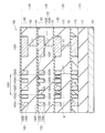
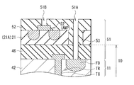
- FIG. 1 illustrates an example of a vertical cross-sectional configuration of a semiconductor device (semiconductor device 100) according to an embodiment of the present disclosure.
- FIG. 2 shows an example of a horizontal sectional configuration of the entire semiconductor device 100 shown in FIG.
- the semiconductor device 100 has, for example, a multilayer wiring structure in which a plurality of wiring layers are stacked, and is applicable to, for example, the imaging device 1 described later.
- the wiring layer 123 having a plurality of wirings (for example, wirings 123X1 to 123X5 and wirings 123Y) extending in one direction (for example, the Z-axis direction), for example, wirings 123X1 to 123X5.
- the insulating layer 132 that forms a gap G is laminated between them.
- the insulating layer 132 has a laminated region 100Y in which an insulating film 132A and an insulating film 132B made of different materials are laminated on a part of the plane, and the laminated region 100Y is provided between the wiring 123X1 and the wiring 123X5. It is provided above the formed gap G.
- the semiconductor device 100 has a configuration in which the first layer 110, the second layer 120, and the third layer 130 are laminated in this order on a support substrate 101 made of, for example, a silicon substrate.
- the first layer 110 and the second layer 120 have a wiring layer 113 and a wiring layer 123, each of which includes a plurality of wirings.
- the insulating layer 111 and the insulating layer 112 are laminated in this order, and the insulating layer 112 is formed by embedding a wiring layer 113 composed of a plurality of wirings (for example, wirings 113X1 to 113X5 and wirings 113Y).
- the insulating layer 111 is formed using, for example, silicon oxide (SiO x ) or silicon nitride (SiN x ).
- the insulating layer 112 is formed using, for example, a low dielectric constant material (Low-k material) having a relative dielectric constant (k) of 2.9 or less.
- the material of the insulating layer 112 include SiOC and the like.
- the wiring layer 113 is composed of, for example, a plurality of wirings extending in one direction, and is composed of, for example, wirings 113X1 to 113X5 and wirings 113Y extending in the Z-axis direction.
- the wirings 113X1 to 113X5 and the wiring 113Y are, for example, embedded in the opening 112H provided in the insulating layer 112, and for example, the barrier metal 113A and the metal for embedding the opening 112H formed in the side surface and the bottom surface of the opening 112H.
- the film 113B examples of the material of the barrier metal 113A include simple substances of Ti (titanium) or Ta (tantalum), alloys thereof, and the like.
- Examples of the material of the metal film 113B include a metal material mainly composed of a low resistance metal such as Cu (copper), W (tungsten) or aluminum (Al).
- an insulating layer 121 and an insulating layer 122 are laminated in this order, and a wiring layer 123 including a plurality of wirings (for example, wiring 123X1 to wiring 123X5 and wiring 123Y) is embedded and formed in the insulating layer 122.
- the wiring layer 123 corresponds to a specific but not limitative example of “first wiring layer” of the present disclosure.
- the insulating layer 121 is formed by using, for example, SiCN.
- the insulating layer 122 is formed by using, for example, a Low-k material having a relative permittivity (k) of 2.9 or less. Specifically, examples of the material of the insulating layer 122 include SiOC.
- the wiring layer 123 is composed of, for example, a plurality of wirings extending in one direction, and is composed of, for example, wirings 123X1 to 123X5 and wirings 123Y extending in the Z-axis direction, similarly to wirings 113X1 to 113X5 and wirings 113Y. ..
- the wirings 123X1 to 123X5 and the wiring 123Y are, for example, embedded in the opening 122H1 provided in the insulating layer 122, and for example, the barrier metal 123A and the metal for embedding the opening 122H1 formed in the side surface and the bottom surface of the opening 122H1. It is composed of a film 123B.
- the material of the barrier metal 123A include simple substances of Ti (titanium) or Ta (tantalum), alloys thereof, and the like.
- Examples of the material of the metal film 123B include a metal material mainly composed of a low resistance metal such as Cu (copper), W (tungsten) or aluminum (Al).
- Wiring 123X1 to 123X5 and wiring 123Y and wiring 113X1 to 113X5 and wiring 113Y of the wiring layer 113 are respectively laminated in the Y-axis direction, and are electrically stacked at a predetermined position via, for example, via V1. It is connected.
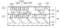
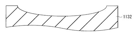
- the third layer 130 has an insulating layer 131 and an insulating layer 132 stacked in this order.
- the insulating layer 131 is formed by using, for example, SiCN.
- the insulating layer 122 constituting the second layer 120 is provided between the wirings of the wiring dense region 100X (for example, between the wirings 123X2 and 123X3, between the wirings 123X3 and 123X4, and the wirings 123X4 and wirings). Between 123X5) has an opening 122H2.
- the insulating layer 131 is continuously provided, for example, on the upper surfaces of the insulating layer 122 and the wirings 123X1 to 123X5 and the wiring 123Y, and the side surfaces and the bottom surface of the opening 122H2.
- the insulating layer 132 is provided on the insulating layer 131.
- the opening 122H2 provided between the wirings of the wiring dense region 100X of the second layer 120 is closed by the insulating layer 132.
- the gap G is formed between the wirings of the second layer 120 (for example, between the wiring 123X2 and the wiring 123X3, between the wiring 123X3 and the wiring 123X4, between the wiring 123X4 and the wiring 123X5).
- the opening 122H2 is formed so as to avoid the via V1 that electrically connects the wiring 113X1 to 113X5 and the wiring 123X1 to 123X5, that is, the region where the gap G is formed (the gap forming region 100Z). ) Is provided in the unformed region of the via V1 in the wiring dense region 100X in which the wirings 123X1 to 123X5 are formed in parallel, as shown in FIG.
- the insulating layer 132 has an insulating film 132 ⁇ /b>A and an insulating film 132 ⁇ /b>B that are partially made of different materials and are stacked in the plane.
- the insulating layer 132 corresponds to a specific example of the "first insulating layer" of the present disclosure, and the insulating film 132A and the insulating film 132B are the "first insulating film” and the "second insulating film” of the present disclosure, respectively.
- the insulating film 132A is formed of, for example, a Low-k material having a relative dielectric constant (k) of 2.9 or less.
- examples of the material of the insulating film 132A include SiOC and the like.
- the insulating film 132B As a material of the insulating film 132B, for example, a material having a higher polishing rate than that of the insulating film 132A is preferably used. Examples of such a material include silicon oxide (SiO x ), SiOC, SiOF or SiON.
- the insulating film 132B may be a single layer film made of any one of the above materials, or may be formed as a laminated film made of two or more kinds. As a result, as will be described in detail later, a part of the insulating film 132A enters along the side surface of the opening 122H2 so as to close the opening 122H2 provided between the wirings of the second layer 120, thereby above the opening 122H2. In other words, the step of the insulating film 132A formed above the void forming region 100Z is filled with the insulating film 132B. Therefore, the insulating layer 132 having a flat surface can be obtained.
- the third layer 130 may be formed by embedding a wiring layer composed of a plurality of wirings on the surface of the insulating layer 132.
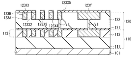
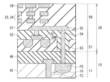
- FIG. 3 illustrates another example of the semiconductor device 100 of the present disclosure.
- a wiring layer 133 composed of a plurality of wirings (for example, wirings 133X1 to 133X5 and wirings 133Y) is embedded in the insulating layer 132 constituting the third layer 130, and the third layer 130 is formed.
- a fourth layer 140 having a wiring layer 143 is further laminated on the layer 130.
- the wiring layer 133 is composed of, for example, a plurality of wirings extending in one direction, and is composed of, for example, wirings 133X1 to 133X5 and wirings 133Y extending in the Z-axis direction, similarly to wirings 113X1 to 113X5 and wirings 113Y. There is.
- the wiring layer 133 corresponds to a specific but not limitative example of “second wiring layer” of the present disclosure.
- At least a part of the wiring 133X1 to the wiring 133X5 is formed in, for example, a laminated region 100Y in which the above-mentioned insulating film 132A and the insulating film 132B are laminated.
- the wiring 133X1 to the wiring 133X5 and the wiring 133Y are, for example, embedded in the opening 132H provided in the insulating layer 132, and for example, the metal for embedding the barrier metal 133A and the opening 122H1 formed on the side surface and the bottom surface of the opening 132H.
- the film 133B examples of the material of the barrier metal 133A include simple substances of Ti (titanium) or Ta (tantalum), alloys thereof, and the like.
- Examples of the material of the metal film 133B include a metal material mainly composed of a low resistance metal such as Cu (copper), W (tungsten) or aluminum (Al).
- the wiring 133Y and the wiring 123Y of the wiring layer 123 are electrically connected to each other via, for example, via V2.
- the insulating layer 141 and the insulating layer 142 are laminated in this order, and the wiring layer 143 composed of a plurality of wirings (for example, wiring 143X1 to wiring 143X5 and wiring 143Y) is embedded in the insulating layer 142.
- the insulating layer 141 is formed using, for example, SiCN.
- the insulating layer 142 is formed by using, for example, a Low-k material having a relative permittivity (k) of 2.9 or less. Specifically, examples of the material of the insulating layer 142 include SiOC and the like.
- the wiring layer 143 is composed of, for example, a plurality of wirings extending in one direction, and is composed of, for example, wirings 143X1 to 143X5 and wirings 143Y extending in the Z-axis direction, similarly to wirings 113X1 to 113X5 and wirings 113Y. There is.
- Wiring 143X1 to Wiring 143X5 and Wiring 143Y are, for example, embedded in an opening 142H provided in an insulating layer 142, and for example, a metal for embedding a barrier metal 143A and an opening 142H formed on the side surface and the bottom surface of the opening 142H. It is composed of a film 143B.
- the material of the barrier metal 143A include simple substances of Ti (titanium) or Ta (tantalum), alloys thereof, and the like.
- Examples of the material of the metal film 143B include a metal material mainly composed of a low resistance metal such as Cu (copper), W (tungsten) or aluminum (Al).
- the wiring 143Y and the wiring 133Y of the wiring layer 133 are electrically connected to each other, for example, via the via V3.
- the insulating layer 111 and the insulating layer 112 are formed in order on the support substrate 101, and then the wiring layer 113 composed of the wirings 113X1 to 113X5 and the wirings 113Y is embedded in the insulating layer 112 to form the first layer 110. Then, the insulating layer 121 and the insulating layer 122 are sequentially formed on the first layer 110. Next, as shown in FIG. 4A, the insulating layer 122 is patterned by, for example, photolithography and etching to form an opening 122H1.
- a barrier metal 123A is formed on the side surface and the bottom surface of the opening 122H1 by sputtering, and then a metal film 123B is formed in the opening 122H1 by plating, and then the surface surface.
- the second layer 120 in which the wirings 123X1 to 123X5 and the wirings 123Y are embedded is formed on the surface of the insulating layer 122.
- the SiCN film 131A and the insulating layer 122 are patterned by, for example, photolithography and etching.
- An opening 122H2 is formed between the wiring 123X2 and the wiring 123X3, between the wiring 123X3 and the wiring 123X4, and between the wiring 123X4 and the wiring 123X5.
- an SiCN film is formed again on the second layer 120 and on the side surface and the bottom surface of the opening 122H2 by using, for example, CVD to form an insulating layer 131 having a film thickness of, for example, 30 nm to 50 nm.
- an insulating film 132A having a film thickness of, for example, 400 nm to 500 nm, which is made of, for example, SiOC, is formed on the entire surface of the second layer 120 by using, for example, CVD.
- the opening 122H2 is closed, and a gap G is formed between the wiring 123X2 and the wiring 123X3, between the wiring 123X3 and the wiring 123X4, and between the wiring 123X4 and the wiring 123X5.
- the insulating film 132B is polished by using, for example, a CMP (Chemical Mechanical Polishing) method.
- the surface of the insulating layer 132 is flattened, and for example, gaps G formed between the wiring 123X2 and the wiring 123X3, between the wiring 123X3 and the wiring 123X4, and between the wiring 123X4 and the wiring 123X5, respectively.
- a laminated region 100Y in which the insulating film 132A and the insulating film 132B are laminated is formed.
- the semiconductor device 100 shown in FIG. 1 is completed.
- the third layer 130 and the fourth layer 140 having the wiring layer 133 and the wiring layer 143 are formed in order on the second layer 120 as in the semiconductor device 100 shown in FIG. 3, for example, It is manufactured as follows.
- the insulating layer 132 is patterned by, for example, photolithography and etching to form an opening 132H.
- sputtering is used to form a barrier metal 133A on the side surface and the bottom surface of the opening 132H, and then, for example, plating is used to form a metal film 133B inside the opening 132H, and then to the surface.
- plating is used to form a metal film 133B inside the opening 132H, and then to the surface.
- the wiring layer 133 including the wirings 133X1 to 133X5 and the wiring 133Y is formed on the surface of the insulating layer 132.
- a SiCN film 141 having a film thickness of 30 nm to 50 nm, for example, 141 is formed on the third layer 130 by, for example, CVD, and then, for example, SiOC (an example of a material) is used.
- An insulating layer 142 having a film thickness of, for example, 400 nm to 500 nm is formed.
- the insulating layer 142 is patterned by photolithography and etching to form the opening 142H.
- the wiring layer 143 is formed by using the same method as the wiring layer 133.
- FIG. 6 illustrates an example of a vertical cross-sectional configuration of the imaging device (imaging device 1) according to the embodiment of the present disclosure.
- FIG. 7 shows an example of a schematic configuration of the image pickup apparatus 1 shown in FIG.
- the image pickup apparatus 1 has a first substrate 10 having a sensor pixel 12 that performs photoelectric conversion on the semiconductor substrate 11, and a readout circuit 22 that outputs an image signal based on the charge output from the sensor pixel 12 on the semiconductor substrate 21. It is an image pickup apparatus having a three-dimensional structure in which a second substrate 20 is laminated.
- the multilayer wiring structure described in the semiconductor device 100 is applied to the wiring layer 56 stacked on the semiconductor substrate 21, for example.
- the image pickup apparatus 1 is a stack of three substrates (first substrate 10, second substrate 20, and third substrate 30) in this order.
- the first substrate 10 includes the semiconductor substrate 11 and the plurality of sensor pixels 12 that perform photoelectric conversion.
- the semiconductor substrate 11 corresponds to a specific but not limitative example of “first semiconductor substrate” of the present disclosure.
- the plurality of sensor pixels 12 are arranged in a matrix in the pixel region 13 of the first substrate 10.
- the second substrate 20 includes, on the semiconductor substrate 21, one reading circuit 22 that outputs a pixel signal based on the charges output from the sensor pixels 12 for each of the four sensor pixels 12.
- the semiconductor substrate 21 corresponds to a specific but not limitative example of “second semiconductor substrate” of the present disclosure.
- the second substrate 20 has a plurality of pixel drive lines 23 extending in the row direction and a plurality of vertical signal lines 24 extending in the column direction.
- the third substrate 30 includes a semiconductor substrate 31 and a logic circuit 32 that processes pixel signals.
- the semiconductor substrate 31 corresponds to a specific but not limitative example of “third semiconductor substrate” of the present disclosure.
- the logic circuit 32 has, for example, a vertical drive circuit 33, a column signal processing circuit 34, a horizontal drive circuit 35, and a system control circuit 36.
- the logic circuit 32 (specifically, the horizontal drive circuit 35) outputs the output voltage Vout for each sensor pixel 12 to the outside.
- a low resistance region made of silicide formed by using a salicide (Self Aligned Silicide) process such as CoSi 2 or NiSi is formed on the surface of the impurity diffusion region in contact with the source electrode and the drain electrode. May be.
- the vertical drive circuit 33 sequentially selects a plurality of sensor pixels 12 row by row, for example.
- the column signal processing circuit 34 performs, for example, Correlated Double Sampling (CDS) processing on the pixel signals output from each sensor pixel 12 in the row selected by the vertical drive circuit 33.
- CDS Correlated Double Sampling
- the column signal processing circuit 34 extracts the signal level of the pixel signal by performing CDS processing, for example, and holds pixel data according to the amount of light received by each sensor pixel 12.
- the horizontal drive circuit 35 sequentially outputs the pixel data held in the column signal processing circuit 34 to the outside, for example.
- the system control circuit 36 controls, for example, the drive of each block (vertical drive circuit 33, column signal processing circuit 34, and horizontal drive circuit 35) in the logic circuit 32.
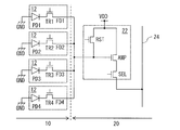
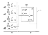
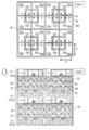
- FIG. 8 shows an example of the sensor pixel 12 and the readout circuit 22.
- shared means that the outputs of the four sensor pixels 12 are input to the common readout circuit 22.
- Each sensor pixel 12 has common constituent elements.
- identification numbers (1, 2, 3, 4) are given to the end of the reference numerals of the constituent elements of each sensor pixel 12.
- an identification number is added to the end of the code of the component of each sensor pixel 12, but the components of each sensor pixel 12 are distinguished from each other.
- the identification number at the end of the reference numeral of the constituent element of each sensor pixel 12 is omitted.
- Each sensor pixel 12 is, for example, a floating diffusion that temporarily holds the electric charge output from the photodiode PD, the transfer transistor TR electrically connected to the photodiode PD, and the electric charge output from the photodiode PD via the transfer transistor TR. It has an FD.
- the photodiode PD corresponds to a specific example of the "photoelectric conversion element" of the present disclosure.
- the photodiode PD performs photoelectric conversion to generate an electric charge according to the amount of received light.
- the cathode of the photodiode PD is electrically connected to the source of the transfer transistor TR, and the anode of the photodiode PD is electrically connected to the reference potential line (eg, ground).
- the drain of the transfer transistor TR is electrically connected to the floating diffusion FD, and the gate of the transfer transistor TR is electrically connected to the pixel drive line 23.
- the transfer transistor TR is, for example, a CMOS (Complementary Metal Oxide Semiconductor) transistor.
- the floating diffusion FDs of the sensor pixels 12 sharing one read circuit 22 are electrically connected to each other and are electrically connected to the input end of the common read circuit 22.
- the read circuit 22 has, for example, a reset transistor RST, a selection transistor SEL, and an amplification transistor AMP.
- the selection transistor SEL may be omitted if necessary.
- the source of the reset transistor RST (the input end of the read circuit 22) is electrically connected to the floating diffusion FD, and the drain of the reset transistor RST is electrically connected to the power line VDD and the drain of the amplification transistor AMP.
- the gate of the reset transistor RST is electrically connected to the pixel drive line 23.
- the source of the amplification transistor AMP is electrically connected to the drain of the selection transistor SEL, and the gate of the amplification transistor AMP is electrically connected to the source of the reset transistor RST.
- the source of the selection transistor SEL (the output end of the readout circuit 22) is electrically connected to the vertical signal line 24, and the gate of the selection transistor SEL is electrically connected to the pixel drive line 23.
- the transfer transistor TR transfers the charge of the photodiode PD to the floating diffusion FD when the transfer transistor TR is turned on.
- the gate of the transfer transistor TR (transfer gate TG) extends from the surface of the semiconductor substrate 11 to a depth that penetrates the p-well 42 and reaches the PD 41.
- the reset transistor RST resets the potential of the floating diffusion FD to a predetermined potential.
- the reset transistor RST is turned on, the potential of the floating diffusion FD is reset to the potential of the power supply line VDD.
- the selection transistor SEL controls the output timing of the pixel signal from the readout circuit 22.
- the amplification transistor AMP generates, as a pixel signal, a signal having a voltage corresponding to the level of the charge held in the floating diffusion FD.
- the amplification transistor AMP constitutes a source follower type amplifier, and outputs a pixel signal having a voltage corresponding to the level of electric charge generated by the photodiode PD.
- the selection transistor SEL When the selection transistor SEL is turned on, the amplification transistor AMP amplifies the potential of the floating diffusion FD and outputs a voltage corresponding to the potential to the column signal processing circuit 34 via the vertical signal line 24.
- the reset transistor RST, the amplification transistor AMP, and the selection transistor SEL are CMOS transistors, for example.
- the selection transistor SEL may be provided between the power supply line VDD and the amplification transistor AMP.
- the drain of the reset transistor RST is electrically connected to the power supply line VDD and the drain of the selection transistor SEL.
- the source of the selection transistor SEL is electrically connected to the drain of the amplification transistor AMP, and the gate of the selection transistor SEL is electrically connected to the pixel drive line 23.
- the source of the amplification transistor AMP (the output end of the readout circuit 22) is electrically connected to the vertical signal line 24, and the gate of the amplification transistor AMP is electrically connected to the source of the reset transistor RST.
- the FD transfer transistor FDG may be provided between the source of the reset transistor RST and the gate of the amplification transistor AMP.
- FD transfer transistor FDG is used when switching the conversion efficiency.
- FIG. 12 shows an example of a connection mode between the plurality of readout circuits 22 and the plurality of vertical signal lines 24.
- the plurality of read circuits 22 are arranged side by side in the extending direction (for example, the column direction) of the vertical signal lines 24, even if one of the plurality of vertical signal lines 24 is assigned to each read circuit 22. Good.
- the four vertical signal lines 24 are the read circuits 22. It may be assigned one for each.
- an identification number (1, 2, 3, 4) is added to the end of the code of each vertical signal line 24.
- the image pickup apparatus 1 has a configuration in which the first substrate 10, the second substrate 20, and the third substrate 30 are laminated in this order, and further, on the back surface (light incident surface) side of the first substrate 10. , A color filter 40 and a light receiving lens 50.
- the color filter 40 and the light receiving lens 50 are provided one by one for each sensor pixel 12, for example. That is, the imaging device 1 is a backside illumination type imaging device.
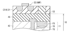
- the first substrate 10 is configured by laminating an insulating layer 46 on the surface (surface 11S1) of the semiconductor substrate 11.
- the first substrate 10 has an insulating layer 46 as a part of the interlayer insulating film 51.
- the insulating layer 46 is provided between the semiconductor substrate 11 and the semiconductor substrate 21 described later.
- the semiconductor substrate 11 is composed of a silicon substrate.
- the semiconductor substrate 11 has, for example, a p-well 42 in a part of the surface or in the vicinity thereof, and in a region other than the p-well 42 (a region deeper than the p-well 42), a conductive type PD 41 different from the p-well 42. have.
- the p well 42 is composed of a p-type semiconductor region.
- the PD 41 is composed of a semiconductor region of a conductivity type (specifically, n type) different from that of the p well 42.
- the semiconductor substrate 11 has a floating diffusion FD in the p-well 42 as a conductive type (specifically, n-type) semiconductor region different from the p-well 42.
- the first substrate 10 has a photodiode PD, a transfer transistor TR, and a floating diffusion FD for each sensor pixel 12.
- the first substrate 10 has a configuration in which a transfer transistor TR and a floating diffusion FD are provided on a part of the surface 11S1 side (the side opposite to the light incident surface side, the second substrate 20 side) of the semiconductor substrate 11. ..
- the first substrate 10 has an element isolation portion 43 that isolates each sensor pixel 12.
- the element isolation portion 43 is formed to extend in the normal direction of the semiconductor substrate 11 (direction perpendicular to the surface of the semiconductor substrate 11).
- the element isolation part 43 is provided between two sensor pixels 12 adjacent to each other.
- the element separating unit 43 electrically separates the sensor pixels 12 adjacent to each other.
- the element isolation portion 43 is made of, for example, silicon oxide.
- the element isolation portion 43 penetrates the semiconductor substrate 11, for example.
- the first substrate 10 further has, for example, a p-well layer 44 which is a side surface of the element separating portion 43 and is in contact with the surface on the photodiode PD side.
- the p well layer 44 is composed of a semiconductor region of a conductivity type (specifically, p type) different from that of the photodiode PD.
- the first substrate 10 further has, for example, a fixed charge film 45 in contact with the back surface (surface 11S2, other surface) of the semiconductor substrate 11.
- the fixed charge film 45 is negatively charged in order to suppress the generation of dark current due to the interface state on the light receiving surface side of the semiconductor substrate 11.
- the fixed charge film 45 is formed of, for example, an insulating film having a negative fixed charge.
- examples of the material for such an insulating film include hafnium oxide, zircon oxide, aluminum oxide, titanium oxide, and tantalum oxide.
- An electric field induced by the fixed charge film 45 forms a hole accumulation layer at the interface of the semiconductor substrate 11 on the light receiving surface side.
- the hole accumulation layer suppresses the generation of electrons from the interface.
- the color filter 40 is provided on the back surface side of the semiconductor substrate 11.
- the color filter 40 is provided, for example, in contact with the fixed charge film 45, and is provided at a position facing the sensor pixel 12 via the fixed charge film 45.
- the light receiving lens 50 is provided, for example, in contact with the color filter 40, and is provided at a position facing the sensor pixel 12 via the color filter 40 and the fixed charge film 45.
- the second substrate 20 is configured by laminating the insulating layer 52 on the semiconductor substrate 21.
- the second substrate 20 has the insulating layer 52 as a part of the interlayer insulating film 51.
- the insulating layer 52 is provided between the semiconductor substrate 21 and the semiconductor substrate 31.
- the semiconductor substrate 21 is composed of a silicon substrate.
- the second substrate 20 has one readout circuit 22 for every four sensor pixels 12.
- the second substrate 20 has a configuration in which the read circuit 22 is provided on a part of the front surface of the semiconductor substrate 21 (the surface 21S1 facing the third substrate 30, the one surface).
- the second substrate 20 is attached to the first substrate 10 with the back surface (surface 21S2) of the semiconductor substrate 21 facing the front surface (surface 11S1) of the semiconductor substrate 11.
- the second substrate 20 is bonded to the first substrate 10 by face-to-back.
- the second substrate 20 further has an insulating layer 53 penetrating the semiconductor substrate 21 in the same layer as the semiconductor substrate 21.
- the second substrate 20 has an insulating layer 53 as a part of the interlayer insulating film 51.
- the insulating layer 53 is provided so as to cover the side surface of the through wiring 54 described later.
- the laminate composed of the first substrate 10 and the second substrate 20 has an interlayer insulating film 51 and a through wiring 54 provided in the interlayer insulating film 51.
- the through wiring 54 corresponds to a specific example of the "first through wiring" of the present disclosure.
- the stacked body has one through wiring 54 for each sensor pixel 12.
- the through wiring 54 extends in the normal direction of the semiconductor substrate 21, and is provided so as to penetrate the portion of the interlayer insulating film 51 including the insulating layer 53.
- the first substrate 10 and the second substrate 20 are electrically connected to each other by a through wiring 54.
- the through wiring 54 is electrically connected to the floating diffusion FD and a connection wiring 55 described later.
- the stacked body including the first substrate 10 and the second substrate 20 further has through wirings 47 and 48 (see FIG. 13 described later) provided in the interlayer insulating film 51.
- the through wirings 47 and 48 correspond to a specific but not limitative example of “second through wiring” in the present disclosure.
- the laminated body has one through wiring 47 and one through wiring 48 for each sensor pixel 12.
- the through wirings 47 and 48 extend in the normal direction of the semiconductor substrate 21, respectively, and are provided so as to penetrate the portion of the interlayer insulating film 51 including the insulating layer 53.
- the first substrate 10 and the second substrate 20 are electrically connected to each other by through wirings 47 and 48.
- the through wiring 47 is electrically connected to the p well 42 of the semiconductor substrate 11 and the wiring in the second substrate 20.
- the through wiring 48 is electrically connected to the transfer gate TG and the pixel drive line 23.
- the second substrate 20 has, for example, a plurality of connecting portions 59 electrically connected to the readout circuit 22 and the semiconductor substrate 21 in the insulating layer 52.
- the second substrate 20 further has, for example, a wiring layer 56 on the insulating layer 52.
- the wiring layer 56 has, for example, an insulating layer 57, a plurality of pixel drive lines 23 provided in the insulating layer 57, and a plurality of vertical signal lines 24.
- the plurality of pixel drive lines 23 correspond to the wirings 113X1 to 113X5 in the semiconductor device 100
- the plurality of vertical signal lines 24 correspond to the wirings 123X1 to 123X5 in the semiconductor device 100.
- a gap G as shown in FIG.
- insulating layer 57 between the wirings of the plurality of vertical signal lines 24. Further, in the insulating layer 57, for example, a laminated region in which insulating films (insulating films 132A and 132B in FIG. 1) made of different materials are laminated on a part of the surface serving as a joint surface with the wiring layer 62 described later is provided. Have. This laminated region is provided between a plurality of pad electrodes 58 described later in FIG. 6, for example. The plurality of pad electrodes 58 correspond to, for example, the wirings 133X1 to 133X5 in the semiconductor device 100.
- the wiring layer 56 further has, for example, a plurality of connection wirings 55 in the insulating layer 57, one for each of the four sensor pixels 12.
- the connection wiring 55 electrically connects each through wiring 54 electrically connected to the floating diffusion FD included in the four sensor pixels 12 sharing the read circuit 22 to each other.
- the total number of the through wirings 54 and 48 is larger than the total number of the sensor pixels 12 included in the first substrate 10, and is twice the total number of the sensor pixels 12 included in the first substrate 10.
- the total number of the through wirings 54, 48, 47 is larger than the total number of the sensor pixels 12 included in the first substrate 10, and is three times the total number of the sensor pixels 12 included in the first substrate 10.
- the wiring layer 56 further has, for example, a plurality of pad electrodes 58 in the insulating layer 57.
- Each pad electrode 58 is made of, for example, a metal such as Cu (copper) or Al (aluminum).
- Each pad electrode 58 is exposed on the surface of the wiring layer 56.
- Each pad electrode 58 is used for electrical connection between the second substrate 20 and the third substrate 30 and for bonding the second substrate 20 and the third substrate 30.
- the plurality of pad electrodes 58 are provided, for example, one for each of the pixel drive line 23 and the vertical signal line 24.
- the total number of pad electrodes 58 (or the total number of bonds between the pad electrodes 58 and the pad electrodes 64 (described later) is smaller than the total number of sensor pixels 12 included in the first substrate 10 ).
- the third substrate 30 is configured by, for example, laminating an interlayer insulating film 61 on a semiconductor substrate 31. As will be described later, the third substrate 30 is attached to the second substrate 20 with the surfaces on the front side facing each other. Therefore, when explaining the configuration inside the third substrate 30, the upper and lower parts will be described. , It is the opposite of the vertical direction in the drawing.
- the semiconductor substrate 31 is composed of a silicon substrate.
- the third substrate 30 has a structure in which a logic circuit 32 is provided on a part of the front surface (face 31S1) of the semiconductor substrate 31.
- the third substrate 30 further has, for example, a wiring layer 62 on the interlayer insulating film 61.
- the wiring layer 62 has, for example, an insulating layer 63 and a plurality of pad electrodes 64 provided in the insulating layer 63.
- the plurality of pad electrodes 64 are electrically connected to the logic circuit 32.
- Each pad electrode 64 is formed of Cu (copper), for example.
- Each pad electrode 64 is exposed on the surface of the wiring layer 62.
- Each pad electrode 64 is used for electrical connection between the second substrate 20 and the third substrate 30 and for bonding the second substrate 20 and the third substrate 30. Further, the pad electrode 64 does not necessarily have to be plural, and even one pad electrode can be electrically connected to the logic circuit 32.
- the second substrate 20 and the third substrate 30 are electrically connected to each other by bonding the pad electrodes 58 and 64 to each other.
- the gate of the transfer transistor TR (transfer gate TG) is electrically connected to the logic circuit 32 via the through wiring 54 and the pad electrodes 58 and 64.
- the third substrate 30 is attached to the second substrate 20 with the surface (surface 31S1) of the semiconductor substrate 31 facing the surface (surface 21S1) side of the semiconductor substrate 21. That is, the third substrate 30 is attached to the second substrate 20 face to face.
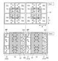
- FIG. 13 and 14 show an example of the cross-sectional configuration of the image pickup apparatus 1 in the horizontal direction.
- 13 and FIG. 14 are diagrams showing an example of the cross-sectional configuration at the cross section Sec1 of FIG. 1, and the bottom diagrams of FIG. 13 and FIG. 14 are the cross-sectional configuration at the cross section Sec2 of FIG. It is a figure which shows an example.
- FIG. 13 illustrates a configuration in which two sets of 2 ⁇ 2 four sensor pixels 12 are arranged in the second direction H
- FIG. 14 shows four sets of 2 ⁇ 2 four sensor pixels 12. A configuration in which they are arranged in the first direction V and the second direction H is illustrated. In the upper sectional views of FIGS.
- FIGS. 13 and 14 a diagram showing an example of the surface configuration of the semiconductor substrate 11 is superimposed on a diagram showing an example of the cross-sectional configuration in the cross section Sec1 of FIG. 1, and the insulating layer 46 Is omitted. Further, in the lower sectional views of FIGS. 13 and 14, a diagram showing an example of the surface configuration of the semiconductor substrate 21 is superimposed on a diagram showing an example of the cross-sectional configuration in the cross-sectional section Sec2 of FIG.
- the plurality of through wirings 54, the plurality of through wirings 48, and the plurality of through wirings 47 are in the plane of the first substrate 10 in the first direction V (vertical direction in FIG. 13, FIG. 14 are arranged side by side in a strip shape.
- FIGS. 13 and 14 illustrate a case where a plurality of through wires 54, a plurality of through wires 48, and a plurality of through wires 47 are arranged side by side in two rows in the first direction V.
- the first direction V is parallel to one of the two arrangement directions (for example, the row direction and the column direction) of the plurality of sensor pixels 12 arranged in a matrix.
- the four floating diffusion FDs are arranged close to each other, for example, via the element separation unit 43.
- the four transfer gates TGs are arranged so as to surround the four floating diffusion FDs, and for example, the four transfer gates TGs form a ring shape. ing.
- the insulating layer 53 is composed of a plurality of blocks extending in the first direction V.
- the semiconductor substrate 21 is composed of a plurality of island-shaped blocks 21A extending in the first direction V and arranged side by side in the second direction H orthogonal to the first direction V via an insulating layer 53. ..
- Each block 21A is provided with, for example, a plurality of sets of reset transistors RST, amplification transistor AMP, and selection transistor SEL.
- One read-out circuit 22 shared by the four sensor pixels 12 is composed of, for example, a reset transistor RST, an amplification transistor AMP, and a selection transistor SEL in a region facing the four sensor pixels 12.
- One readout circuit 22 shared by the four sensor pixels 12 includes, for example, an amplification transistor AMP in the block 21A adjacent to the left of the insulating layer 53, a reset transistor RST in the block 21A adjacent to the right of the insulating layer 53, and a selection transistor RST. It is composed of a transistor SEL.
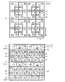
- FIG. 15, FIG. 16, FIG. 17, and FIG. 18 show an example of the wiring layout in the horizontal plane of the image pickup apparatus 1.
- 15 to 18 illustrate a case where one readout circuit 22 shared by the four sensor pixels 12 is provided in a region facing the four sensor pixels 12.
- the wirings shown in FIGS. 15 to 18 are provided in different layers of the wiring layer 56, for example.
- the four through wires 54 adjacent to each other are electrically connected to the connection wiring 55, for example, as shown in FIG.
- the four penetrating wirings 54 adjacent to each other are further connected to the gate of the amplification transistor AMP included in the left adjacent block 21A of the insulating layer 53 via the connecting wiring 55 and the connecting portion 59, as shown in FIG. 15, for example.
- And is electrically connected to the gate of the reset transistor RST included in the right adjacent block 21A of the insulating layer 53.
- the power supply line VDD is arranged at a position facing each read circuit 22 arranged side by side in the second direction H.
- the power line VDD is electrically connected to the drain of the amplification transistor AMP and the drain of the reset transistor RST of each readout circuit 22 arranged side by side in the second direction H via the connection portion 59. Is connected.
- the two pixel drive lines 23 are arranged at positions facing each of the read-out circuits 22 arranged side by side in the second direction H.
- One pixel drive line 23 (second control line) is electrically connected to the gate of the reset transistor RST of each read circuit 22 arranged side by side in the second direction H, for example, as shown in FIG. Wiring RSTG.
- the other pixel drive line 23 (third control line) is electrically connected to the gate of the selection transistor SEL of each readout circuit 22 arranged side by side in the second direction H, for example, as shown in FIG. Wiring SELG.
- the source of the amplification transistor AMP and the drain of the selection transistor SEL are electrically connected to each other via the wiring 25, for example, as shown in FIG.
- the two power supply lines VSS are arranged at positions facing the respective read circuits 22 arranged side by side in the second direction H, as shown in FIG. 17, for example.
- each power line VSS is electrically connected to a plurality of through wirings 47 at a position facing each sensor pixel 12 arranged side by side in the second direction H, for example.
- the four pixel drive lines 23 are arranged at positions facing the respective readout circuits 22 arranged side by side in the second direction H.
- Each of the four pixel drive lines 23 is, for example, one of the four sensor pixels 12 corresponding to the respective readout circuits 22 arranged side by side in the second direction H, as shown in FIG.
- the wiring TRG is electrically connected to the twelve through wirings 48.
- the four pixel drive lines 23 are electrically connected to the gate (transfer gate TG) of the transfer transistor TR of each sensor pixel 12 arranged side by side in the second direction H. ..
- an identifier (1, 2, 3, 4) is given to the end of each wiring TRG.
- the vertical signal line 24 is arranged at a position facing each read circuit 22 arranged side by side in the first direction V.
- the vertical signal line 24 (output line) is electrically connected to the output end (source of the amplification transistor AMP) of each read circuit 22 arranged side by side in the first direction V. ing.
- the p well 42, the element isolation portion 43, and the p well layer 44 are formed on the semiconductor substrate 11.
- the photodiode PD, the transfer transistor TR, and the floating diffusion FD are formed on the semiconductor substrate 11 (FIG. 19A).
- the sensor pixel 12 is formed on the semiconductor substrate 11.
- a material having high heat resistance include polysilicon.
- the insulating layer 46 is formed on the semiconductor substrate 11 (FIG. 19A). In this way, the first substrate 10 is formed.
- the semiconductor substrate 21 is bonded onto the first substrate 10 (insulating layer 46B) (FIG. 19B). Then, the semiconductor substrate 21 is thinned if necessary. At this time, the thickness of the semiconductor substrate 21 is set to a film thickness required for forming the readout circuit 22.
- the thickness of the semiconductor substrate 21 is generally about several hundreds nm. However, depending on the concept of the read circuit 22, an FD (Fully Depletion) type is also possible, and in that case, the thickness of the semiconductor substrate 21 can be in the range of several nm to several ⁇ m.
- the insulating layer 53 is formed in the same layer as the semiconductor substrate 21 (FIG. 19C).
- the insulating layer 53 is formed, for example, at a position facing the floating diffusion FD.
- a slit (opening 21H) penetrating the semiconductor substrate 21 is formed in the semiconductor substrate 21 to separate the semiconductor substrate 21 into a plurality of blocks 21A.
- the insulating layer 53 is formed so as to fill the slit.
- a readout circuit 22 including an amplification transistor AMP and the like is formed in each block 21A of the semiconductor substrate 21 (FIG. 19C).
- the gate insulating film of the readout circuit 22 can be formed by thermal oxidation.
- the insulating layer 52 is formed on the semiconductor substrate 21.
- the interlayer insulating film 51 composed of the insulating layers 46, 52, 53 is formed.
- through holes 51A and 51B are formed in the interlayer insulating film 51 (FIG. 19D).
- a through hole 51B penetrating the insulating layer 52 is formed at a portion of the insulating layer 52 facing the reading circuit 22.
- a through hole 51A penetrating the interlayer insulating film 51 is formed at a portion facing the floating diffusion FD (that is, a portion facing the insulating layer 53).
- the through wiring 54 is formed in the through hole 51A and the connecting portion 59 is formed in the through hole 51B (FIG. 19E). Further, on the insulating layer 52, the connection wiring 55 that electrically connects the through wiring 54 and the connection portion 59 to each other is formed (FIG. 19E). Then, the wiring layer 56 is formed on the insulating layer 52 (FIG. 19F). In this way, the second substrate 20 is formed.
- the second substrate 20 is attached to the third substrate 30 on which the logic circuit 32 and the wiring layer 62 are formed, with the surface of the semiconductor substrate 21 facing the surface side of the semiconductor substrate 31 (FIG. 19G).
- the pad electrode 58 of the second substrate 20 and the pad electrode 64 of the third substrate 30 are joined to each other to electrically connect the second substrate 20 and the third substrate 30 to each other. In this way, the image pickup apparatus 1 is manufactured.
- a step is formed on the surface of the insulating layer 1132 above the gap, for example, as shown in FIG. 20A.
- the insulating layer 1132 formed using the Low-k material generally has a low polishing rate.
- the step portion is preferentially polished as shown in FIG. 20B.
- the global step will deteriorate and the thickness of the insulating layer 1132 will vary widely in the plane. Deterioration of the global level difference and variation of the film thickness of the insulating layer 1132 within the surface cause variation of the wiring capacitance within the semiconductor device and variation of device characteristics between two or more semiconductor devices.
- the plurality of wirings 123X1 to 123X5 and the wiring 123Y that are formed in parallel in the Z-axis direction are stacked on the second layer 120, and the plurality of wirings 123X1 to 123X5 are formed.
- the insulating layer 132 forming the gap G between them was formed as a laminated film in which an insulating film 132A and an insulating film 132B made of different materials are laminated in a part of the plane.
- the laminated region 100Y in which the insulating film 132A and the insulating film 132B are laminated is provided above the gap G formed between the plurality of wirings 123X1 and 123X5.
- the insulating film 132A is more than the insulating film 132A.
- the insulating film 132B formed by using a material having a high polishing rate is further laminated. Then, for example, as shown in FIG. 21B, the surface is polished using, for example, the CMP method.
- the insulating film 132A is formed on the second layer 120, the insulating film 132A is formed on the surface of the insulating film 132A by entering into the openings 122H2 formed between the plurality of wirings 123X1 to 123X5.
- the step is buried by the insulating film 132B, and the surface of the third layer 130 can be flattened. That is, the variation in the film thickness of the insulating layer 132 in the plane is reduced.
- the insulating layer 132 for example, the wiring layer 133 of the second layer 120, for example, in the Z-axis direction.
- the imaging device 1 having excellent device characteristics.
- FIG. 22 illustrates an example of a vertical cross-sectional configuration of an imaging device (imaging device 1) according to a modification (modification 1) of the above embodiment.
- the transfer transistor TR has a planar transfer gate TG. Therefore, the transfer gate TG does not penetrate the p well 42 and is formed only on the surface of the semiconductor substrate 11. Even when the planar transfer gate TG is used for the transfer transistor TR, the imaging device 1 has the same effect as the above-described embodiment.
- FIG. 23 illustrates an example of a vertical cross-sectional configuration of an imaging device (imaging device 1) according to a modification (modification 2) of the above embodiment.
- the second substrate 20 and the third substrate 30 are electrically connected to each other in a region of the first substrate 10 facing the peripheral region 14.
- the peripheral region 14 corresponds to the frame region of the first substrate 10 and is provided on the periphery of the pixel region 13.
- the second substrate 20 has a plurality of pad electrodes 58 in the region facing the peripheral region 14, and the third substrate 30 has a plurality of pad electrodes 58 in the region facing the peripheral region 14. It has 64.
- the second substrate 20 and the third substrate 30 are electrically connected to each other by the bonding of the pad electrodes 58 and 64 provided in the region facing the peripheral region 14.
- the second substrate 20 and the third substrate 30 are electrically connected to each other by joining the pad electrodes 58 and 64 provided in the region facing the peripheral region 14.
- the pad electrodes 58 and 64 are bonded to each other in the region facing the pixel region 13. Therefore, in addition to the effects of the above-described embodiment, it is possible to provide the image pickup device 1 having a three-layer structure that does not hinder the miniaturization of the area per pixel with the same chip size as before.
- FIG. 24 illustrates an example of a vertical cross-sectional configuration of an imaging device (imaging device 1) according to a modification (modification 3) of the above embodiment.
- FIG. 25 illustrates another example of the vertical cross-sectional configuration of the imaging device (imaging device 1) according to the modification (modification 3) of the above embodiment.
- the upper view of FIGS. 24 and 25 is a modification of the cross-sectional configuration of the cross section Sec1 of FIG. 1, and the lower view of FIG. 24 is a modification of the cross-sectional configuration of the cross section Sec2 of FIG. is there.
- FIG. 1 is superimposed on a diagram showing a modified example of the cross-sectional configuration of the cross section Sec1 of FIG.
- the insulating layer 46 is omitted.
- a diagram showing a modified example of the surface configuration of the semiconductor substrate 21 is superimposed on a diagram showing a modified example of the cross-sectional configuration in the cross-sectional section Sec2 of FIG. There is.
- the plurality of through wires 54, the plurality of through wires 48, and the plurality of through wires 47 are the surfaces of the first substrate 10. Inside, they are arranged side by side in a strip shape in the first direction V (the left-right direction in FIGS. 24 and 25). Note that FIGS. 24 and 25 illustrate a case where a plurality of through wires 54, a plurality of through wires 48, and a plurality of through wires 47 are arranged side by side in two rows in the first direction V. In the four sensor pixels 12 sharing the readout circuit 22, the four floating diffusion FDs are arranged close to each other, for example, via the element separation unit 43.
- the four transfer gates TGs (TG1, TG2, TG3, TG4) are arranged so as to surround the four floating diffusion FDs, for example, the four transfer gates TGs. It has a ring shape.
- the insulating layer 53 is composed of a plurality of blocks extending in the first direction V.
- the semiconductor substrate 21 is composed of a plurality of island-shaped blocks 21A extending in the first direction V and arranged side by side in the second direction H orthogonal to the first direction V via an insulating layer 53. ..
- Each block 21A is provided with, for example, a reset transistor RST, an amplification transistor AMP, and a selection transistor SEL.
- One read-out circuit 22 shared by the four sensor pixels 12 is not arranged facing the four sensor pixels 12, for example, but is arranged so as to be offset in the second direction H.
- one read-out circuit 22 shared by the four sensor pixels 12 is a reset transistor in the second substrate 20 in which the region facing the four sensor pixels 12 is shifted in the second direction H. It is composed of an RST, an amplification transistor AMP and a selection transistor SEL.
- One readout circuit 22 shared by the four sensor pixels 12 is configured of, for example, the amplification transistor AMP, the reset transistor RST, and the selection transistor SEL in one block 21A.
- one read-out circuit 22 shared by the four sensor pixels 12 is a reset transistor in the second substrate 20 in which a region facing the four sensor pixels 12 is shifted in the second direction H. It is composed of RST, amplification transistor AMP, selection transistor SEL and FD transfer transistor FDG.
- One read-out circuit 22 shared by the four sensor pixels 12 is composed of, for example, an amplification transistor AMP, a reset transistor RST, a selection transistor SEL, and an FD transfer transistor FDG in one block 21A.
- one readout circuit 22 shared by the four sensor pixels 12 is not arranged to face the four sensor pixels 12, for example, and is second from a position facing the four sensor pixels 12. They are arranged so as to be offset in the direction H.
- the wiring 25 can be shortened, or the wiring 25 can be omitted and the source of the amplification transistor AMP and the drain of the selection transistor SEL can be configured in a common impurity region. ..
- FIG. 26 illustrates an example of a horizontal cross-sectional configuration of an imaging device (imaging device 1) according to a modification (modification 4) of the above embodiment.
- FIG. 26 shows a modified example of the cross-sectional configuration of FIG.
- the semiconductor substrate 21 is composed of a plurality of island-shaped blocks 21A arranged side by side in the first direction V and the second direction H via the insulating layer 53.
- Each block 21A is provided with, for example, a set of reset transistor RST, amplification transistor AMP, and selection transistor SEL.
- the crosstalk between the readout circuits 22 adjacent to each other can be suppressed by the insulating layer 53, and the deterioration of the image quality due to the resolution reduction and the color mixing on the reproduced image can be suppressed.
- FIG. 27 illustrates an example of a horizontal cross-sectional configuration of an imaging device (imaging device 1) according to a modification (modification 5) of the above embodiment.
- FIG. 27 shows a modified example of the cross-sectional configuration of FIG. 26.
- one read circuit 22 shared by the four sensor pixels 12 is not arranged, for example, directly facing the four sensor pixels 12, but is arranged so as to be displaced in the first direction V.
- the semiconductor substrate 21 is composed of a plurality of island-shaped blocks 21A arranged side by side in the first direction V and the second direction H via the insulating layer 53. There is.
- Each block 21A is provided with, for example, a set of reset transistor RST, amplification transistor AMP, and selection transistor SEL.
- the plurality of through wirings 47 and the plurality of through wirings 54 are further arranged in the second direction H.
- the plurality of through wirings 47 share four through wirings 54 that share a certain read circuit 22 and four through wirings that share another read circuit 22 adjacent to the read circuit 22 in the second direction H. 54 and 54.
- the crosstalk between the read circuits 22 adjacent to each other can be suppressed by the insulating layer 53 and the through wiring 47, and the deterioration of the resolution on the reproduced image and the deterioration of the image quality due to the color mixture can be suppressed. Can be done.
- FIG. 28 illustrates an example of a horizontal cross-sectional configuration of an imaging device (imaging device 1) according to a modification (modification 6) of the above embodiment.
- FIG. 28 shows a modified example of the cross-sectional configuration of FIG.
- the first substrate 10 has the photodiode PD and the transfer transistor TR for each sensor pixel 12, and the floating diffusion FD is shared by every four sensor pixels 12. Therefore, in this modification, one through wiring 54 is provided for each of the four sensor pixels 12.
- the first substrate 10 shares the through wiring 47 for each of the four sensor pixels 12A. Therefore, in this modified example, one through wiring 47 is provided for every four sensor pixels 12A.
- the first substrate 10 has an element isolation section 43 that isolates the photodiode PD and the transfer transistor TR for each sensor pixel 12.
- the element separation unit 43 does not completely surround the sensor pixel 12 when viewed from the normal direction of the semiconductor substrate 11, and has a gap (through wiring 54) and a gap (through wiring 47) in the vicinity of the floating diffusion FD (through wiring 54). (Unformed area). The gap allows the four sensor pixels 12 to share one through wiring 54 and the four sensor pixels 12A to share one through wiring 47.
- the second substrate 20 has the readout circuit 22 for each of the four sensor pixels 12 that share the floating diffusion FD.
- FIG. 29 illustrates another example of the horizontal cross-sectional configuration of the image pickup apparatus 1 according to the present modification.
- FIG. 29 shows a modification of the sectional configuration of FIG.
- the first substrate 10 has the photodiode PD and the transfer transistor TR for each sensor pixel 12, and the floating diffusion FD is shared by every four sensor pixels 12. Further, the first substrate 10 has an element isolation section 43 that isolates the photodiode PD and the transfer transistor TR for each sensor pixel 12.
- FIG. 30 illustrates another example of the horizontal cross-sectional configuration of the imaging device 1 according to the present modification.
- FIG. 30 shows a modification of the sectional configuration of FIG.
- the first substrate 10 has the photodiode PD and the transfer transistor TR for each sensor pixel 12, and the floating diffusion FD is shared by every four sensor pixels 12. Further, the first substrate 10 has an element isolation section 43 that isolates the photodiode PD and the transfer transistor TR for each sensor pixel 12.
- FIG. 31 shows an example of the circuit configuration of the imaging device (imaging device 1) according to the above-described embodiment and the modified examples (modified example 7) of the modified examples 1 to 6.
- the image pickup apparatus 1 according to this modification is a CMOS image sensor equipped with a column parallel ADC.
- the imaging device 1 in addition to the pixel region 13 in which a plurality of sensor pixels 12 including photoelectric conversion elements are two-dimensionally arranged in a matrix (matrix), vertical driving is performed.
- the circuit 33, the column signal processing circuit 34, the reference voltage supply unit 38, the horizontal drive circuit 35, the horizontal output line 37, and the system control circuit 36 are provided.
- the system control circuit 36 is based on the master clock MCK, and is a clock signal or control that serves as a reference for the operation of the vertical drive circuit 33, the column signal processing circuit 34, the reference voltage supply unit 38, the horizontal drive circuit 35, and the like.
- a signal or the like is generated and given to the vertical drive circuit 33, the column signal processing circuit 34, the reference voltage supply unit 38, the horizontal drive circuit 35, and the like.
- the vertical drive circuit 33 is also formed on the first substrate 10 together with the sensor pixels 12 in the pixel region 13, and is also formed on the second substrate 20 on which the readout circuit 22 is formed.
- the column signal processing circuit 34, the reference voltage supply unit 38, the horizontal drive circuit 35, the horizontal output line 37, and the system control circuit 36 are formed on the third substrate 30.
- the sensor pixel 12 has, for example, a configuration including a photodiode PD and a transfer transistor TR that transfers charges obtained by photoelectric conversion in the photodiode PD to the floating diffusion FD.
- the readout circuit 22 includes, for example, a reset transistor RST that controls the potential of the floating diffusion FD, an amplification transistor AMP that outputs a signal corresponding to the potential of the floating diffusion FD, and pixel selection.
- a 3-transistor configuration having a selection transistor SEL for performing the above can be used.
- the sensor pixels 12 are two-dimensionally arranged, and the pixel drive lines 23 are arranged in each row and the vertical signal lines 24 are arranged in each column with respect to the pixel arrangement of m rows and n columns. There is.
- One end of each of the plurality of pixel drive lines 23 is connected to each output end corresponding to each row of the vertical drive circuit 33.
- the vertical drive circuit 33 is composed of a shift register or the like, and controls the row address and the row scan of the pixel region 13 via the plurality of pixel drive lines 23.
- the column signal processing circuit 34 has, for example, ADCs (analog-digital conversion circuits) 34-1 to 34-m provided for each pixel column of the pixel region 13, that is, for each vertical signal line 24.
- ADCs analog-digital conversion circuits
- the reference voltage supply unit 38 has, for example, a DAC (digital-to-analog conversion circuit) 38A as a means for generating a reference voltage Vref of a so-called ramp (RAMP) waveform whose level changes in an inclined manner over time.
- DAC digital-to-analog conversion circuit
- the means for generating the reference voltage Vref having the ramp waveform is not limited to the DAC 38A.
- the DAC38A Under the control of the control signal CS1 given by the system control circuit 36, the DAC38A generates a reference voltage Vref of the lamp waveform based on the clock CK given by the system control circuit 36, and the ADC 34- of the column signal processing circuit 34. Supply for 1 to 34-m.
- the exposure time of the sensor pixel 12 is 1 / N as compared with the normal frame rate mode in the progressive scanning method for reading the information of all the sensor pixels 12 and the normal frame rate mode.
- the switching of the operation mode is executed under the control of the control signals CS2 and CS3 provided from the system control circuit 36. Further, the system control circuit 36 is provided with instruction information for switching between the normal frame rate mode and each operation mode of the high frame rate mode from an external system controller (not shown).
- the ADC 34-m is configured to include a comparator 34A, a counting means such as an up / down counter (denoted as U / DNT in the figure) 34B, a transfer switch 34C, and a memory device 34D.
- a comparator 34A a counting means such as an up / down counter (denoted as U / DNT in the figure) 34B, a transfer switch 34C, and a memory device 34D.
- the comparator 34A has a signal voltage Vx of the vertical signal line 24 corresponding to the signal output from each sensor pixel 12 in the nth column of the pixel area 13 and a reference voltage Vref of the lamp waveform supplied from the reference voltage supply unit 38.
- Vref the reference voltage
- the output Vco becomes the "H" level
- the reference voltage Vref is equal to or less than the signal voltage Vx
- the output Vco becomes the "L" level. ..
- the up / down counter 34B is an asynchronous counter, and a clock CK is given from the system control circuit 36 at the same time as the DAC18A under the control by the control signal CS2 given from the system control circuit 36, and is down in synchronization with the clock CK ( By performing the DOWN) count or the UP (UP) count, the comparison period from the start of the comparison operation in the comparator 34A to the end of the comparison operation is measured.
- the comparison time at the first read time is measured by down-counting at the first read operation, and the second read operation is performed.
- the comparison time at the time of the second reading is measured by performing an upcount at the time of the reading operation of.
- the count result for the sensor pixel 12 in a certain row is held as it is, and then the sensor pixel 12 in the next row is down-counted from the previous count result at the first read operation.
- the comparison time at the time of the first read is measured, and by counting up at the time of the second read operation, the comparison time at the time of the second read is measured.
- the transfer switch 34C is turned on (in the normal frame rate mode) when the counting operation of the up / down counter 34B for the sensor pixel 12 in a certain row is completed under the control by the control signal CS3 given from the system control circuit 36. In the closed state, the count result of the up / down counter 34B is transferred to the memory device 34D.
- the analog signal supplied from each sensor pixel 12 in the pixel region 13 via the vertical signal line 24 for each column is converted into the analog signal of the comparator 34A and the up/down counter 34B in the ADCs 34-1 to 34-m. By each operation, it is converted into an N-bit digital signal and stored in the memory device 34D.
- the horizontal drive circuit 35 is composed of a shift register or the like, and controls the column address and column scan of the ADCs 34-1 to 34-m in the column signal processing circuit 34. Under the control of the horizontal drive circuit 35, the N-bit digital signal AD-converted by each of the ADCs 34-1 to 34-m is sequentially read out to the horizontal output line 37, and passes through the horizontal output line 37. It is output as imaging data.
- a circuit or the like for performing various kinds of signal processing on the imaging data output via the horizontal output line 37 may be provided in addition to the above-described constituent elements. Is.
- the count result of the up / down counter 34B can be selectively transferred to the memory apparatus 34D via the transfer switch 34C, so that the up / down counter 34B can be up / down. It is possible to independently control the count operation of the down counter 34B and the read operation of the count result of the up/down counter 34B to the horizontal output line 37.
- FIG. 32 shows an example in which the image pickup apparatus of FIG. 31 is formed by stacking three substrates (first substrate 10, second substrate 20, third substrate 30).
- first substrate 10 a pixel region 13 including a plurality of sensor pixels 12 is formed in the central portion, and a vertical drive circuit 33 is formed around the pixel region 13.
- second substrate 20 a read circuit region 15 including a plurality of read circuits 22 is formed in the central portion, and a vertical drive circuit 33 is formed around the read circuit region 15.
- a column signal processing circuit 34, a horizontal drive circuit 35, a system control circuit 36, a horizontal output line 37, and a reference voltage supply unit 38 are formed on the third substrate 30.
- the vertical drive circuit 33 may be formed only on the first substrate 10 or only on the second substrate 20.
- FIG. 33 shows an example of the cross-sectional configuration of the imaging device (imaging device 1) according to the above-described embodiment and the modified examples (modified 9) of the modified examples 1 to 8.
- the image pickup apparatus 1 is configured by laminating three substrates (first substrate 10, second substrate 20, third substrate 30).
- the two substrates may be laminated.
- the logic circuit 32 may be formed separately in the first substrate 10 and the second substrate 20, as shown in FIG. 33, for example.
- a high dielectric constant film made of a material (for example, high-k) capable of withstanding a high temperature process and a metal gate electrode are laminated.
- a transistor having a gate structure is provided.
- the circuit 32B provided on the second substrate 20 side from the silicide formed on the surface of the impurity diffusion region in contact with the source electrode and the drain electrode by using a salicide (Self Aligned Silicide) process such as CoSi 2 or NiSi.
- the low resistance region 26 is formed.
- the low resistance region made of silicide is formed of a compound of a material of the semiconductor substrate and a metal.
- a high temperature process such as thermal oxidation can be used.
- a low resistance region 26 made of VDD is provided on the surface of the impurity diffusion region in contact with the source electrode and the drain electrode, contact is made. The resistance can be reduced. As a result, the calculation speed in the logic circuit 32 can be increased.
- FIG. 34 shows a modified example of the cross-sectional configuration of the image pickup apparatus 1 according to the first to fourth embodiments and the modified examples 1 to 8 thereof (modified example 10).
- a salicide (Self Aligned Silicide) process such as CoSi 2 or NiSi is performed on the surface of the impurity diffusion region in contact with the source electrode and the drain electrode.
- a low resistance region 37 made of VDD formed by using the above may be formed. Accordingly, when forming the sensor pixel 12, a high temperature process such as thermal oxidation can be used.
- the contact resistance can be reduced. As a result, the operation speed in the logic circuit 32 can be increased.
- the conductivity types may be reversed in the above-described embodiment and the modified examples 1 to 10.
- the p-type may be read as the n-type and the n-type may be read as the p-type. Even in such a case, the same effects as those of the above-described first to fifth embodiments and their modifications 1 to 10 can be obtained.
- FIG. 35 shows an example of a schematic configuration of an imaging system 7 including an imaging device (imaging device 1) according to the above-described embodiment and modifications 1 to 10 thereof.
- the imaging system 7 is, for example, an imaging device such as a digital still camera or a video camera, or an electronic device such as a mobile terminal device such as a smartphone or a tablet type terminal.
- the image pickup system 7 includes, for example, an optical system 241, a shutter device 242, an image pickup device 1, a DSP circuit 243, a frame memory 244, a display unit 245, a storage unit 246, an operation unit 247, and a power supply unit 248.
- the shutter device 242, the image pickup device 1, the DSP circuit 243, the frame memory 244, the display unit 245, the storage unit 246, the operation unit 247, and the power supply unit 248 are connected to each other via a bus line 249. ..
- the image pickup device 1 outputs image data according to incident light.
- the optical system 241 has one or a plurality of lenses, and guides light (incident light) from a subject to the imaging device 1 and forms an image on the light receiving surface of the imaging device 1.
- the shutter device 242 is arranged between the optical system 241 and the imaging device 1, and controls the light irradiation period and the light blocking period of the imaging device 1 under the control of the operation unit 247.
- the DSP circuit 243 is a signal processing circuit that processes a signal (image data) output from the imaging device 1.
- the frame memory 244 temporarily holds the image data processed by the DSP circuit 243 in frame units.
- the display unit 245 includes, for example, a panel-type display device such as a liquid crystal panel or an organic EL (Electro Luminescence) panel, and displays a moving image or a still image captured by the imaging device 1.
- the storage unit 246 records image data of a moving image or a still image captured by the image capturing apparatus 1 in a recording medium such as a semiconductor memory or a hard disk.
- the operation unit 247 issues operation commands for various functions of the imaging system 7 according to the operation by the user.
- the power supply unit 248 appropriately supplies various power sources serving as operating power sources for the image pickup device 1, the DSP circuit 243, the frame memory 244, the display unit 245, the storage unit 246, and the operation unit 247 to these supply targets.
- FIG. 36 shows an example of a flowchart of the imaging operation in the imaging system 7.
- the user instructs the start of imaging by operating the operation unit 247 (step S101).
- the operation unit 247 transmits an imaging command to the imaging device 1 (step S102).
- the image pickup apparatus 1 specifically, the system control circuit 36
- the image pickup device 1 outputs the light (image data) formed on the light receiving surface via the optical system 241 and the shutter device 242 to the DSP circuit 243.
- the image data is data for all pixels of the pixel signal generated based on the electric charge temporarily held in the floating diffusion FD.
- the DSP circuit 243 performs predetermined signal processing (for example, noise reduction processing) based on the image data input from the image pickup apparatus 1 (step S104).
- the DSP circuit 243 causes the frame memory 244 to hold the image data subjected to the predetermined signal processing, and the frame memory 244 causes the storage unit 246 to store the image data (step S105). In this way, the image pickup by the image pickup system 7 is performed.
- the imaging device 1 is applied to the imaging system 7.
- the image pickup apparatus 1 can be made smaller or have a higher definition, so that the image pickup system 7 having a smaller size or a higher definition can be provided.
- FIG. 37 is a diagram showing an outline of a configuration example of a non-stacked solid-state image sensor (solid-state image sensor 23210) and a stacked solid-state image sensor (solid-state image sensor 23020) to which the technique according to the present disclosure can be applied.
- FIG. 37A shows a schematic configuration example of a non-stacked solid-state image sensor.
- the solid-state imaging device 23010 has one die (semiconductor substrate) 23011 as shown in A of FIG.
- the die 23011 includes a pixel region 23012 in which pixels are arranged in an array, a control circuit 23013 for driving pixels and various other controls, and a logic circuit 23014 for signal processing.
- B and C in FIG. 37 show a schematic configuration example of a stacked solid-state image sensor.
- the solid-state image sensor 23020 is configured as one semiconductor chip by stacking two dies, a sensor die 23021 and a logic die 23024, and electrically connecting them.
- the sensor No. 23021 and the logic die 23024 correspond to specific examples of the “first substrate” and the “second substrate” of the present disclosure.
- the sensor die 23021 is equipped with a pixel region 23012 and a control circuit 23013, and the logic die 23024 is equipped with a logic circuit 23014 including a signal processing circuit that performs signal processing. Further, the sensor 20321 may be equipped with, for example, the reading circuit 22 described above.
- the sensor die 23021 is mounted with the pixel region 23012
- the logic die 23024 is mounted with the control circuit 23013 and the logic circuit 23014.
- FIG. 38 is a sectional view showing a first configuration example of the stacked solid-state imaging device 23020.
- the sensor die 23021 is formed with PDs (photodiodes), FDs (floating diffusion), Trs (MOS FETs), and Trs, which are control circuits 23013, that form pixels in the pixel area 23012. Further, the sensor die 23021 is formed with a wiring layer 23101 having a plurality of layers, in this example, three layers of wiring 23110. Note that the control circuit 23013 (which becomes Tr) can be configured in the logic die 23024 instead of the sensor die 23021.
- a Tr constituting the logic circuit 23014 is formed on the logic die 23024.
- the logic die 23024 is formed with a wiring layer 23161 having a plurality of layers, in this example, three layers of wiring 23170.
- the logic die 23024 is formed with a connection hole 23171 in which an insulating film 23172 is formed on the inner wall surface, and a connection conductor 23173 connected to the wiring 23170 or the like is embedded in the connection hole 23171.
- the sensor die 23021 and the logic die 23024 are attached to each other so that the wiring layers 23101 and 23161 face each other, thereby forming a laminated solid-state image sensor 23020 in which the sensor die 23021 and the logic die 23024 are laminated.
- a film 23191 such as a protective film is formed on a surface where the sensor die 23021 and the logic die 23024 are attached to each other.
- the sensor die 23021 is formed with a connection hole 23111 that penetrates the sensor die 23021 from the back surface side (the side where light is incident on the PD) (upper side) of the sensor die 23021 and reaches the wiring 23170 on the uppermost layer of the logic die 23024. Further, in the sensor die 23021, a connection hole 23121 is formed near the connection hole 23111 and reaching the wiring 23110 of the first layer from the back surface side of the sensor die 23021. An insulating film 23112 is formed on the inner wall surface of the connection hole 23111, and an insulating film 23122 is formed on the inner wall surface of the connection hole 23121. Then, the connecting conductors 23113 and 23123 are embedded in the connecting holes 23111 and 23121, respectively.
- the connecting conductor 23113 and the connecting conductor 23123 are electrically connected to each other on the back surface side of the sensor die 23021, whereby the sensor die 23021 and the logic die 23024 are connected to the wiring layer 23101, the connection hole 23121, the connection hole 23111, and the wiring layer. It is electrically connected via 23161.
- 39 is a cross-sectional view showing a second configuration example of the stacked solid-state imaging device 23020.
- the sensor die 23021 (wiring layer 23101 (wiring 23110)) and the logic die 23024 (wiring layer 23161 (wiring) are provided by one connection hole 2321 formed in the sensor die 23021. 23170)) is electrically connected.
- connection hole 2321 is formed so as to penetrate the sensor die 23021 from the back surface side of the sensor die 23021 and reach the wiring 23170 on the uppermost layer of the logic die 23024 and reach the wiring 23110 on the uppermost layer of the sensor die 23021. Will be done.
- An insulating film 23212 is formed on the inner wall surface of the connection hole 23211, and a connection conductor 23213 is embedded in the connection hole 23211.
- the sensor die 23021 and the logic die 23024 are electrically connected by the two connection holes 23111 and 23121, but in FIG. 39, the sensor die 23021 and the logic die 23024 are connected by one connection hole 23211. It is electrically connected.
- FIG. 40 is a cross-sectional view showing a third configuration example of the stacked solid-state imaging device 23020.
- the solid-state image sensor 23020 of FIG. 40 has a surface on which the sensor die 23021 and the logic die 23024 are bonded, in that a film 23191 such as a protective film is not formed on the surface on which the sensor die 23021 and the logic die 23024 are bonded. This is different from the case of FIG. 38 in which a film 23191 such as a protective film is formed.
- the sensor die 23021 and the logic die 23024 are overlapped with each other so that the wirings 23110 and 23170 are in direct contact with each other, heated while applying the required load, and the wirings 23110 and 23170 are directly joined. It is composed.
- FIG. 41 is a cross-sectional view showing another configuration example of the stacked solid-state imaging device to which the technology according to the present disclosure can be applied.
- the solid-state image sensor 23401 has a three-layer laminated structure in which three dies of a sensor die 23411, a logic die 23412, and a memory die 23413 are laminated.
- the memory die 23413 has, for example, a memory circuit that stores data that is temporarily necessary for signal processing performed by the logic die 23412.
- the logic die 23412 and the memory die 23413 are stacked under the sensor die 23411 in that order.
- the logic die 23412 and the memory die 23413 are arranged in the reverse order, that is, the memory die 23413 and the logic die 23412 in the order. It can be laminated below 23411.
- the sensor die 23411 is formed with a PD serving as a photoelectric conversion unit of a pixel and a source/drain region of the pixel Tr.
- a gate electrode is formed around the PD via a gate insulating film, and a pixel Tr 23421 and a pixel Tr 23422 are formed by a source/drain region paired with the gate electrode.
- the pixel Tr23421 adjacent to the PD is the transfer Tr, and one of the source/drain regions of the pair forming the pixel Tr23421 is the FD.
- An interlayer insulating film is formed on the sensor die 23411, and a connection hole is formed in the interlayer insulating film.
- a pixel Tr 23421 and a connection conductor 23431 connected to the pixel Tr 23422 are formed in the connection hole.
- the sensor die 23411 is formed with a wiring layer 23433 having a plurality of layers of wiring 23432 connected to each connection conductor 23431.
- an aluminum pad 23434 serving as an electrode for external connection is formed on the lowermost layer of the wiring layer 23433 of the sensor die 23411. That is, in the sensor die 23411, the aluminum pad 23434 is formed at a position closer to the bonding surface 23440 to the logic die 23412 than the wiring 23432.
- the aluminum pad 23434 is used as one end of the wiring related to the input / output of a signal to the outside.
- the sensor die 23411 is formed with a contact 23441 used for electrical connection with the logic die 23412.
- the contact 23441 is connected to the contact 23451 of the logic die 23412 and also to the aluminum pad 23442 of the sensor die 23411.
- the sensor die 23411 is formed with a pad hole 23443 so as to reach the aluminum pad 23442 from the back surface side (upper side) of the sensor die 23411.
- the wiring 23110 and the wiring layer 23161 may be provided with, for example, the plurality of pixel drive lines 23 and the plurality of vertical signal lines 24 described above.
- the gap G as shown in FIG. 1 between the wirings of the plurality of vertical signal lines 24, it is possible to reduce the capacitance between the wirings. Further, by suppressing the increase in the capacity between the wirings, it is possible to reduce the variation in the wiring capacity.
- Application example 1 The technology according to the present disclosure (this technology) can be applied to various products.
- the technology according to the present disclosure is realized as a device mounted on a moving body of any kind such as an automobile, an electric vehicle, a hybrid electric vehicle, a motorcycle, a bicycle, a personal mobility, an airplane, a drone, a ship, and a robot. May be.
- FIG. 42 is a block diagram showing a schematic configuration example of a vehicle control system that is an example of a mobile body control system to which the technology according to the present disclosure can be applied.
- the vehicle control system 12000 includes a plurality of electronic control units connected via a communication network 12001.
- the vehicle control system 12000 includes a drive system control unit 12010, a body system control unit 12020, an outside information detection unit 12030, an in-vehicle information detection unit 12040, and an integrated control unit 12050.
- a microcomputer 12051, an audio/video output unit 12052, and an in-vehicle network I/F (interface) 12053 are shown as the functional configuration of the integrated control unit 12050.
- the drive system control unit 12010 controls the operation of devices related to the drive system of the vehicle according to various programs.
- the drive system control unit 12010 provides a driving force generator for generating the driving force of the vehicle such as an internal combustion engine or a driving motor, a driving force transmission mechanism for transmitting the driving force to the wheels, and a steering angle of the vehicle. It functions as a steering mechanism for adjustment and a control device such as a braking device that generates a braking force of the vehicle.
- the body system control unit 12020 controls the operation of various devices mounted on the vehicle body according to various programs.
- the body system control unit 12020 functions as a keyless entry system, a smart key system, a power window device, or a control device for various lamps such as headlamps, back lamps, brake lamps, blinkers or fog lamps.
- the body system control unit 12020 may be input with radio waves transmitted from a portable device that substitutes for the key or signals of various switches.
- the body system control unit 12020 receives inputs of these radio waves or signals and controls a vehicle door lock device, a power window device, a lamp, and the like.
- the vehicle exterior information detection unit 12030 detects information outside the vehicle equipped with the vehicle control system 12000.
- the imaging unit 12031 is connected to the vehicle outside information detection unit 12030.
- the vehicle exterior information detection unit 12030 causes the image capturing unit 12031 to capture an image of the vehicle exterior and receives the captured image.
- the vehicle exterior information detection unit 12030 may perform object detection processing or distance detection processing such as people, vehicles, obstacles, signs, or characters on the road surface based on the received image.
- the imaging unit 12031 is an optical sensor that receives light and outputs an electric signal according to the amount of the light received.
- the imaging unit 12031 can output the electric signal as an image or as distance measurement information.
- the light received by the imaging unit 12031 may be visible light or invisible light such as infrared light.
- the in-vehicle information detection unit 12040 detects in-vehicle information.
- a driver state detection unit 12041 that detects the state of the driver is connected.
- the driver state detection unit 12041 includes, for example, a camera that images the driver, and the in-vehicle information detection unit 12040 determines the degree of fatigue or concentration of the driver based on the detection information input from the driver state detection unit 12041. It may be calculated or it may be determined whether the driver is asleep.
- the microcomputer 12051 calculates the control target value of the driving force generator, the steering mechanism, or the braking device based on the information inside and outside the vehicle acquired by the vehicle exterior information detection unit 12030 or the vehicle interior information detection unit 12040, and the drive system control unit.
- a control command can be output to 12010.
- the microcomputer 12051 realizes a function of ADAS (Advanced Driver Assistance System) that includes collision avoidance or impact mitigation of a vehicle, follow-up traveling based on an inter-vehicle distance, vehicle speed maintenance traveling, a vehicle collision warning, or a vehicle lane departure warning. It is possible to perform cooperative control for the purpose.
- ADAS Advanced Driver Assistance System
- the microcomputer 12051 controls the driving force generator, the steering mechanism, the braking device, and the like based on the information around the vehicle acquired by the vehicle exterior information detection unit 12030 or the vehicle interior information detection unit 12040. It is possible to perform cooperative control for the purpose of autonomous driving or the like that autonomously travels without depending on operation.
- the microcomputer 12051 can output a control command to the body system control unit 12020 based on the information outside the vehicle acquired by the outside information detection unit 12030.
- the microcomputer 12051 controls the headlamps according to the position of the preceding vehicle or the oncoming vehicle detected by the external information detection unit 12030, and performs cooperative control for the purpose of antiglare such as switching the high beam to the low beam. It can be carried out.
- the voice image output unit 12052 transmits an output signal of at least one of a voice and an image to an output device capable of visually or audibly notifying information to an occupant of the vehicle or the outside of the vehicle.
- an audio speaker 12061, a display unit 12062, and an instrument panel 12063 are illustrated as output devices.
- the display unit 12062 may include, for example, at least one of an onboard display and a head-up display.
- FIG. 43 is a diagram showing an example of the installation position of the imaging unit 12031.
- the vehicle 12100 includes image pickup units 12101, 12102, 12103, 12104, 12105 as the image pickup unit 12031.
- the imaging units 12101, 12102, 12103, 12104, 12105 are provided at positions such as the front nose, side mirrors, rear bumpers, back doors, and the upper part of the windshield in the vehicle interior of the vehicle 12100, for example.
- the image capturing unit 12101 provided on the front nose and the image capturing unit 12105 provided on the upper part of the windshield in the vehicle interior mainly acquire an image in front of the vehicle 12100.
- the imaging units 12102 and 12103 included in the side mirrors mainly acquire images of the side of the vehicle 12100.
- the imaging unit 12104 provided on the rear bumper or the back door mainly acquires an image of the rear of the vehicle 12100.
- the front images acquired by the imaging units 12101 and 12105 are mainly used for detecting a preceding vehicle or a pedestrian, an obstacle, a traffic signal, a traffic sign, a lane, or the like.
- FIG. 43 shows an example of the photographing range of the imaging units 12101 to 12104.
- the imaging range 12111 indicates the imaging range of the imaging unit 12101 provided on the front nose
- the imaging ranges 12112 and 12113 indicate the imaging ranges of the imaging units 12102 and 12103 provided on the side mirrors
- the imaging range 12114 indicates The imaging range of the imaging part 12104 provided in a rear bumper or a back door is shown.
- a bird's-eye view image of the vehicle 12100 viewed from above can be obtained.
- At least one of the image capturing units 12101 to 12104 may have a function of acquiring distance information.
- at least one of the image capturing units 12101 to 12104 may be a stereo camera including a plurality of image capturing elements, or may be an image capturing element having pixels for phase difference detection.
- the microcomputer 12051 has a distance to each three-dimensional object within the imaging range 12111 to 12114 based on the distance information obtained from the imaging units 12101 to 12104, and a temporal change of this distance (relative velocity with respect to the vehicle 12100).
- a predetermined speed for example, 0 km / h or more.
- the microcomputer 12051 can set an inter-vehicle distance to be secured in front of the preceding vehicle in advance, and can perform automatic braking control (including follow-up stop control), automatic acceleration control (including follow-up start control), and the like. In this way, it is possible to perform cooperative control for the purpose of autonomous driving or the like that autonomously travels without depending on the operation of the driver.
- the microcomputer 12051 converts three-dimensional object data related to a three-dimensional object into two-wheeled vehicles, ordinary vehicles, large vehicles, pedestrians, electric poles, and other three-dimensional objects based on the distance information obtained from the imaging units 12101 to 12104. It can be classified and extracted and used for automatic avoidance of obstacles. For example, the microcomputer 12051 identifies an obstacle around the vehicle 12100 into an obstacle visible to the driver of the vehicle 12100 and an obstacle difficult to see. Then, the microcomputer 12051 determines the collision risk indicating the risk of collision with each obstacle, and when the collision risk is equal to or higher than the set value and there is a possibility of collision, the microcomputer 12051 via the audio speaker 12061 or the display unit 12062. By outputting an alarm to the driver and performing forced deceleration and avoidance steering via the drive system control unit 12010, driving support for collision avoidance can be provided.
- At least one of the imaging units 12101 to 12104 may be an infrared camera that detects infrared rays.
- the microcomputer 12051 can recognize a pedestrian by determining whether or not a pedestrian is present in the images captured by the imaging units 12101 to 12104.
- pedestrian recognition includes, for example, a procedure for extracting feature points in an image captured by an imaging unit 12101 to 12104 as an infrared camera, and pattern matching processing for a series of feature points indicating the outline of an object to determine whether or not the pedestrian is a pedestrian. Is performed by the procedure for determining.
- the audio image output unit 12052 When the microcomputer 12051 determines that a pedestrian is present in the captured images of the imaging units 12101 to 12104 and recognizes the pedestrian, the audio image output unit 12052 outputs a square contour line for emphasizing the recognized pedestrian.
- the display unit 12062 is controlled so as to superimpose and display. Further, the audio image output unit 12052 may control the display unit 12062 so as to display an icon or the like indicating a pedestrian at a desired position.
- the above is an example of a mobile control system to which the technology according to the present disclosure can be applied.
- the technology according to the present disclosure can be applied to the imaging unit 12031 among the configurations described above.
- the imaging device 1 according to the above-described embodiment and its modification can be applied to the imaging unit 12031.
- FIG. 44 is a diagram illustrating an example of a schematic configuration of an endoscopic surgery system to which the technology (the technology) according to the present disclosure can be applied.
- FIG. 44 illustrates a situation in which an operator (doctor) 11131 is operating on a patient 11132 on a patient bed 11133 using the endoscopic surgery system 11000.
- the endoscopic surgery system 11000 includes an endoscope 11100, other surgical tools 11110 such as a pneumoperitoneum tube 11111 and an energy treatment tool 11112, and a support arm device 11120 that supports the endoscope 11100.
- a cart 11200 equipped with various devices for endoscopic surgery.
- the endoscope 11100 is composed of a lens barrel 11101 into which a region having a predetermined length from the distal end is inserted into the body cavity of the patient 11132, and a camera head 11102 connected to the base end of the lens barrel 11101.
- the endoscope 11100 configured as a so-called rigid mirror having the rigid barrel 11101 is illustrated, but the endoscope 11100 may be configured as a so-called flexible mirror having a flexible barrel. Good.
- An opening in which an objective lens is fitted is provided at the tip of the lens barrel 11101.
- a light source device 11203 is connected to the endoscope 11100, and the light generated by the light source device 11203 is guided to the tip of the lens barrel by a light guide extending inside the lens barrel 11101 to be an objective.
- the observation target in the body cavity of the patient 11132 is once irradiated through the lens.
- the endoscope 11100 may be a direct-viewing endoscope, or may be a perspective or side-viewing endoscope.
- An optical system and an image pickup device are provided inside the camera head 11102, and the reflected light (observation light) from the observation target is condensed on the image pickup device by the optical system.
- the observation light is photoelectrically converted by the imaging element, and an electric signal corresponding to the observation light, that is, an image signal corresponding to the observation image is generated.
- the image signal is transmitted to the camera control unit (CCU: Camera Control Unit) 11201 as RAW data.
- the CCU11201 is composed of a CPU (Central Processing Unit), a GPU (Graphics Processing Unit), and the like, and comprehensively controls the operations of the endoscope 11100 and the display device 11202. Further, the CCU 11201 receives an image signal from the camera head 11102, and performs various image processes on the image signal for displaying an image based on the image signal, such as development processing (demosaic processing).
- a CPU Central Processing Unit
- GPU Graphics Processing Unit
- the display device 11202 displays an image based on an image signal subjected to image processing by the CCU 11201 under the control of the CCU 11201.
- the light source device 11203 is composed of, for example, a light source such as an LED (Light Emitting Diode), and supplies irradiation light to the endoscope 11100 when photographing an operating part or the like.
- a light source such as an LED (Light Emitting Diode)
- LED Light Emitting Diode
- the input device 11204 is an input interface for the endoscopic surgery system 11000.
- the user can input various information and input instructions to the endoscopic surgery system 11000 via the input device 11204.
- the user inputs an instruction to change the imaging conditions (type of irradiation light, magnification, focal length, etc.) by the endoscope 11100.
- the treatment tool control device 11205 controls the drive of the energy treatment tool 11112 for cauterizing, incising, sealing a blood vessel, or the like of a tissue.
- the pneumoperitoneum device 11206 is used to inflate the body cavity of the patient 11132 through the pneumoperitoneum tube 11111 in order to inflate the body cavity of the patient 11132 for the purpose of securing the visual field by the endoscope 11100 and the working space of the operator.
- the recorder 11207 is a device capable of recording various information related to surgery.
- the printer 11208 is a device that can print various types of information regarding surgery in various formats such as text, images, or graphs.
- the light source device 11203 that supplies the irradiation light to the endoscope 11100 when photographing the surgical site can be composed of, for example, an LED, a laser light source, or a white light source composed of a combination thereof.
- a white light source is configured by combining RGB laser light sources, the output intensity and output timing of each color (each wavelength) can be controlled with high accuracy. Therefore, the light source device 11203 adjusts the white balance of the captured image. It can be carried out.
- the laser light from each of the RGB laser light sources is irradiated to the observation target in a time-division manner, and the drive of the image sensor of the camera head 11102 is controlled in synchronization with the irradiation timing to support each of RGB. It is also possible to capture the image in a time-division manner. According to this method, a color image can be obtained without providing a color filter on the image sensor.
- the drive of the light source device 11203 may be controlled so as to change the intensity of the output light at predetermined time intervals.
- the drive of the image sensor of the camera head 11102 in synchronization with the timing of changing the light intensity to acquire an image in a time-division manner and synthesizing the image, so-called high dynamic without blackout and overexposure. Images of the range can be generated.
- the light source device 11203 may be configured to be able to supply light in a predetermined wavelength band corresponding to special light observation.
- special light observation for example, by utilizing the wavelength dependence of light absorption in body tissue to irradiate light in a narrow band as compared with the irradiation light (that is, white light) in normal observation, the mucosal surface layer.
- a so-called narrow band imaging is performed in which a predetermined tissue such as a blood vessel is photographed with high contrast.
- fluorescence observation in which an image is obtained by the fluorescence generated by irradiating the excitation light may be performed.
- the body tissue is irradiated with excitation light to observe the fluorescence from the body tissue (autofluorescence observation), or a reagent such as indocyanine green (ICG) is locally injected into the body tissue and the body tissue is injected. It is possible to obtain a fluorescence image by irradiating excitation light corresponding to the fluorescence wavelength of the reagent.
- the light source device 11203 may be configured to be capable of supplying narrow band light and / or excitation light corresponding to such special light observation.
- FIG. 45 is a block diagram showing an example of the functional configuration of the camera head 11102 and the CCU 11201 shown in FIG.
- the camera head 11102 includes a lens unit 11401, an imaging unit 11402, a driving unit 11403, a communication unit 11404, and a camera head control unit 11405.
- CCU11201 has a communication unit 11411, an image processing unit 11412, and a control unit 11413.
- the camera head 11102 and CCU11201 are communicatively connected to each other by a transmission cable 11400.
- the lens unit 11401 is an optical system provided at a connection portion with the lens barrel 11101.
- the observation light taken in from the tip of the lens barrel 11101 is guided to the camera head 11102 and enters the lens unit 11401.
- the lens unit 11401 is configured by combining a plurality of lenses including a zoom lens and a focus lens.
- the image pickup unit 11402 includes an image pickup element.
- the image sensor constituting the image pickup unit 11402 may be one (so-called single plate type) or a plurality (so-called multi-plate type).
- each image pickup element may generate an image signal corresponding to each of RGB, and a color image may be obtained by synthesizing them.
- the image pickup unit 11402 may be configured to have a pair of image pickup elements for acquiring image signals for the right eye and the left eye corresponding to 3D (Dimensional) display, respectively.
- the 3D display enables the operator 11131 to more accurately grasp the depth of the biological tissue in the surgical site.
- a plurality of lens units 11401 may be provided corresponding to each image pickup element.
- the image pickup unit 11402 does not necessarily have to be provided in the camera head 11102.
- the imaging unit 11402 may be provided inside the lens barrel 11101 immediately after the objective lens.
- the drive unit 11403 is composed of an actuator, and moves the zoom lens and the focus lens of the lens unit 11401 by a predetermined distance along the optical axis under the control of the camera head control unit 11405. Accordingly, the magnification and focus of the image captured by the image capturing unit 11402 can be adjusted as appropriate.
- the communication unit 11404 is composed of a communication device for transmitting/receiving various information to/from the CCU 11201.
- the communication unit 11404 transmits the image signal obtained from the image pickup unit 11402 as RAW data to the CCU 11201 via the transmission cable 11400.
- the communication unit 11404 receives a control signal for controlling the drive of the camera head 11102 from the CCU 11201 and supplies the control signal to the camera head control unit 11405.
- the control signal includes, for example, information to specify the frame rate of the captured image, information to specify the exposure value at the time of imaging, and / or information to specify the magnification and focus of the captured image. Contains information about the condition.
- the image capturing conditions such as the frame rate, the exposure value, the magnification, and the focus may be appropriately designated by the user, or may be automatically set by the control unit 11413 of the CCU 11201 based on the acquired image signal. Good.
- the endoscope 11100 is equipped with so-called AE (Auto Exposure) function, AF (Auto Focus) function, and AWB (Auto White Balance) function.
- the camera head control unit 11405 controls the driving of the camera head 11102 based on the control signal from the CCU 11201 received via the communication unit 11404.
- the communication unit 11411 is composed of a communication device for transmitting and receiving various information to and from the camera head 11102.
- the communication unit 11411 receives the image signal transmitted from the camera head 11102 via the transmission cable 11400.
- the communication unit 11411 transmits a control signal for controlling the driving of the camera head 11102 to the camera head 11102.
- Image signals and control signals can be transmitted by telecommunications, optical communication, or the like.
- the image processing unit 11412 performs various types of image processing on the image signal that is the RAW data transmitted from the camera head 11102.
- the control unit 11413 performs various controls regarding imaging of a surgical site or the like by the endoscope 11100 and display of a captured image obtained by imaging the surgical site or the like. For example, the control unit 11413 generates a control signal for controlling the driving of the camera head 11102.
- the control unit 11413 also causes the display device 11202 to display a captured image of the surgical site or the like based on the image signal subjected to the image processing by the image processing unit 11412. At this time, the control unit 11413 may recognize various objects in the captured image by using various image recognition techniques. For example, the control unit 11413 detects the shape, color, etc. of the edge of an object included in the captured image to remove surgical tools such as forceps, a specific biological part, bleeding, mist when using the energy treatment tool 11112, and the like. Can be recognized. When displaying the captured image on the display device 11202, the control unit 11413 may superimpose and display various surgical support information on the image of the surgical unit by using the recognition result. By superimposing and displaying the operation support information and presenting it to the operator 11131, it is possible to reduce the burden on the operator 11131 and to allow the operator 11131 to proceed with the operation reliably.
- various image recognition techniques For example, the control unit 11413 detects the shape, color, etc. of the edge
- the transmission cable 11400 that connects the camera head 11102 and the CCU 11201 is an electric signal cable that supports electric signal communication, an optical fiber that supports optical communication, or a composite cable of these.
- wired communication is performed using the transmission cable 11400, but communication between the camera head 11102 and the CCU 11201 may be performed wirelessly.
- the above is an example of an endoscopic surgery system to which the technology according to the present disclosure can be applied.
- the technology according to the present disclosure can be suitably applied to the imaging unit 11402 provided in the camera head 11102 of the endoscope 11100 among the configurations described above.
- the image capturing unit 11402 can be downsized or high-definition, and thus a compact or high-definition endoscope 11100 can be provided.
- the present disclosure has been described above with reference to the embodiments and the modifications 1 to 10 thereof, application examples, and application examples, the present disclosure is not limited to the above-described embodiments and the like, and various modifications can be made. ..
- the plurality of pixel drive lines 23 extend in the row direction and the plurality of vertical signal lines extend in the column direction in the above embodiments and the like, they may extend in the same direction. .. Further, the extending direction of the pixel drive line 23 can be changed as appropriate, such as in the vertical direction.
- the present technology has been described by taking the imaging device 1 having a three-dimensional structure as an example, but the present invention is not limited to this.
- the present technology can be applied to any three-dimensional stacked large-scale integrated (LSI) semiconductor device.
- LSI large-scale integrated
- the present disclosure may also have the following structure.
- the present technology having the following configuration, on the first wiring layer having a plurality of first wirings extending in one direction, there are voids between the plurality of first wirings, and different materials are provided above the voids.
- the first insulating layer having a stacked region in which the first insulating film and the second insulating film are stacked is provided. This reduces the in-plane variation in film thickness of the first insulating layer. Therefore, it is possible to reduce the variation in the wiring capacity.
- the first insulating film is formed of a low dielectric constant material having a relative dielectric constant k of 2.9 or less.
- the semiconductor device according to any one of (1) to (3), wherein the second insulating film is formed using silicon oxide (SiO x ), SiOC, SiOF, or SiON.
- the first insulating layer is provided with a second wiring layer having a plurality of second wirings extending in the same direction as the plurality of first wirings provided in the first wiring layer, The semiconductor device according to any one of (1) to (4).
- (6) The semiconductor device according to (5), wherein at least a part of the second wiring layer is embedded in the stacked region.
- a first substrate having sensor pixels for photoelectric conversion on the first semiconductor substrate The second semiconductor substrate has a readout circuit that outputs a pixel signal based on the electric charge output from the sensor pixel, has a multilayer wiring layer that is laminated on the second semiconductor substrate, and is laminated on the first substrate.
- the multilayer wiring layer is A first wiring layer having a plurality of first wirings extending in one direction, A first insulating layer, which forms a void in at least a part of the plurality of wirings, and has a laminated region in which a first insulating film and a second insulating film made of different materials are laminated above the void.
- An imaging device in which layers are stacked.
- the image pickup device according to (8), wherein the second substrate further includes a logic circuit that processes the pixel signal.
- the third semiconductor substrate further includes a third substrate having at least one of a logic circuit that processes the pixel signal and a memory circuit that holds the pixel signal,
- the imaging device according to (8) or (9), wherein the first substrate, the second substrate, and the third substrate are laminated in this order.
- the third substrate penetrates the third semiconductor substrate by bonding the pad electrodes to each other.
- the imaging device according to (10), wherein the imaging device is electrically connected to each other by the second through wiring when the second through wiring is provided.
- the sensor pixel includes a photoelectric conversion element, a transfer transistor electrically connected to the photoelectric conversion element, and a floating diffusion that temporarily holds charges output from the photoelectric conversion element via the transfer transistor.
- the readout circuit includes a reset transistor that resets a potential of the floating diffusion to a predetermined potential, an amplification transistor that generates, as the pixel signal, a signal of a voltage corresponding to a level of charges held in the floating diffusion,
- the imaging device according to (11) further including a selection transistor that controls an output timing of the pixel signal from the amplification transistor.
- the first substrate has a configuration in which the photoelectric conversion element, the transfer transistor, and the floating diffusion are provided on one surface side of the first semiconductor substrate facing the second substrate
- the second substrate has a configuration in which the read circuit is provided on one surface side of the second semiconductor substrate, and the front second semiconductor is provided on the one surface side of the first semiconductor substrate.
- the imaging device according to (12) which is attached to the first substrate with the other surface of the substrate facing the one surface facing the other surface.
- the third substrate has a configuration in which the logic circuit is provided on one surface side of the third semiconductor substrate, and the third semiconductor substrate is provided on the one surface side of the second semiconductor substrate.
- the imaging device according to (13) which is attached to the second substrate with the other surface facing the one surface facing the other side.
- a laminated body including the first substrate and the second substrate includes an interlayer insulating film between the first semiconductor substrate and the second semiconductor substrate, and a first through wiring provided in the interlayer insulating film. Have The gate of the transfer transistor is electrically connected to the logic circuit via the first through wire and the pad electrode or the second through wire, according to (14) or (15). Imaging device.
- An interlayer insulating film is provided between the first semiconductor substrate and the second semiconductor substrate, and the first substrate has a gate wiring extending in a direction parallel to the first substrate in the interlayer insulating film.
- the imaging device according to any one of (14) to (16), wherein the gate of the transfer transistor is electrically connected to the logic circuit via the gate wiring.
- the second substrate has the readout circuit for each of the four sensor pixels.
- the imaging device according to (16) or (17), wherein the plurality of first through wirings are arranged side by side in a strip shape in the first direction on the surface of the first substrate.
- the sensor pixels are arranged in a matrix in the first direction and a second direction orthogonal to the first direction,
- the second substrate is A first control line electrically connected to a gate of a transfer transistor of each of the sensor pixels arranged side by side in the second direction;
- a second control line electrically connected to the gates of the reset transistors arranged side by side in the second direction;
- a third control line electrically connected to a gate of each of the selection transistors arranged side by side in the second direction,
- the second substrate further includes a plurality of pixel drive lines extending in the one direction, and a plurality of vertical signal lines extending in a vertical direction of the plurality of pixel drive lines,
- the imaging device according to any one of (8) to (19), wherein the void is provided in at least a part between wirings of the plurality of vertical signal lines.
- a first semiconductor substrate having a sensor pixel that performs photoelectric conversion and a readout circuit that outputs a pixel signal based on an electric charge output from the sensor pixel, and a first multilayer wiring layer laminated on the first semiconductor substrate.
- An imaging device in which layers are stacked.
- the first substrate further includes a plurality of pixel drive lines extending in the one direction, and a plurality of vertical signal lines extending in a vertical direction of the plurality of pixel drive lines,
Landscapes
- Engineering & Computer Science (AREA)
- Power Engineering (AREA)
- Physics & Mathematics (AREA)
- General Physics & Mathematics (AREA)
- Condensed Matter Physics & Semiconductors (AREA)
- Computer Hardware Design (AREA)
- Microelectronics & Electronic Packaging (AREA)
- Electromagnetism (AREA)
- Manufacturing & Machinery (AREA)
- Signal Processing (AREA)
- Multimedia (AREA)
- Internal Circuitry In Semiconductor Integrated Circuit Devices (AREA)
- Solid State Image Pick-Up Elements (AREA)
Abstract
Selon un mode de réalisation de la présente invention, un dispositif à semi-conducteur est pourvu d'une première couche de fils comprenant une pluralité de premiers fils s'étendant dans une direction, et d'une première couche isolante disposée sur la première couche de fils, la première couche isolante formant un entrefer au moins partiellement entre la pluralité de fils, et présentant une région empilée sur l'entrefer dans laquelle un premier film isolant et un second film isolant qui sont constitués de matériaux différents sont empilés.
Priority Applications (2)
| Application Number | Priority Date | Filing Date | Title |
|---|---|---|---|
| JP2021503968A JPWO2020179494A1 (fr) | 2019-03-07 | 2020-02-21 | |
| US17/433,796 US20220123040A1 (en) | 2019-03-07 | 2020-02-21 | Semiconductor device and imaging unit |
Applications Claiming Priority (2)
| Application Number | Priority Date | Filing Date | Title |
|---|---|---|---|
| JP2019-041133 | 2019-03-07 | ||
| JP2019041133 | 2019-03-07 |
Publications (1)
| Publication Number | Publication Date |
|---|---|
| WO2020179494A1 true WO2020179494A1 (fr) | 2020-09-10 |
Family
ID=72337942
Family Applications (1)
| Application Number | Title | Priority Date | Filing Date |
|---|---|---|---|
| PCT/JP2020/007048 WO2020179494A1 (fr) | 2019-03-07 | 2020-02-21 | Dispositif à semi-conducteur et dispositif d'imagerie |
Country Status (4)
| Country | Link |
|---|---|
| US (1) | US20220123040A1 (fr) |
| JP (1) | JPWO2020179494A1 (fr) |
| TW (1) | TW202044486A (fr) |
| WO (1) | WO2020179494A1 (fr) |
Cited By (3)
| Publication number | Priority date | Publication date | Assignee | Title |
|---|---|---|---|---|
| WO2022249596A1 (fr) * | 2021-05-26 | 2022-12-01 | ソニーセミコンダクタソリューションズ株式会社 | Élément d'imagerie et procédé de production d'élément d'imagerie |
| WO2022254824A1 (fr) * | 2021-05-31 | 2022-12-08 | ソニーセミコンダクタソリューションズ株式会社 | Élément d'imagerie |
| TWI817390B (zh) * | 2021-12-15 | 2023-10-01 | 南亞科技股份有限公司 | 具有複合中介結構的光學半導體元件 |
Citations (8)
| Publication number | Priority date | Publication date | Assignee | Title |
|---|---|---|---|---|
| JP2004193431A (ja) * | 2002-12-12 | 2004-07-08 | Renesas Technology Corp | 半導体装置およびその製造方法 |
| JP2006261440A (ja) * | 2005-03-17 | 2006-09-28 | Nec Electronics Corp | 半導体装置およびその製造方法 |
| US20070018075A1 (en) * | 2005-07-21 | 2007-01-25 | Stmicroelectronics S.A. | Image sensor |
| JP2012015400A (ja) * | 2010-07-02 | 2012-01-19 | Canon Inc | 固体撮像装置 |
| JP2013232647A (ja) * | 2012-04-27 | 2013-11-14 | Taiwan Semiconductor Manufacturing Co Ltd | 縦方向に集積化される背面照射型イメージセンサ装置 |
| US20140138752A1 (en) * | 2012-08-10 | 2014-05-22 | Taiwan Semiconductor Manufacturing Company, Ltd. | System and Method for Fabricating a 3D Image Sensor Structure |
| JP2014236183A (ja) * | 2013-06-05 | 2014-12-15 | 株式会社東芝 | イメージセンサ装置及びその製造方法 |
| JP2015023150A (ja) * | 2013-07-19 | 2015-02-02 | ルネサスエレクトロニクス株式会社 | 半導体装置の製造方法 |
-
2020
- 2020-02-21 JP JP2021503968A patent/JPWO2020179494A1/ja active Pending
- 2020-02-21 US US17/433,796 patent/US20220123040A1/en active Pending
- 2020-02-21 WO PCT/JP2020/007048 patent/WO2020179494A1/fr active Application Filing
- 2020-02-27 TW TW109106401A patent/TW202044486A/zh unknown
Patent Citations (8)
| Publication number | Priority date | Publication date | Assignee | Title |
|---|---|---|---|---|
| JP2004193431A (ja) * | 2002-12-12 | 2004-07-08 | Renesas Technology Corp | 半導体装置およびその製造方法 |
| JP2006261440A (ja) * | 2005-03-17 | 2006-09-28 | Nec Electronics Corp | 半導体装置およびその製造方法 |
| US20070018075A1 (en) * | 2005-07-21 | 2007-01-25 | Stmicroelectronics S.A. | Image sensor |
| JP2012015400A (ja) * | 2010-07-02 | 2012-01-19 | Canon Inc | 固体撮像装置 |
| JP2013232647A (ja) * | 2012-04-27 | 2013-11-14 | Taiwan Semiconductor Manufacturing Co Ltd | 縦方向に集積化される背面照射型イメージセンサ装置 |
| US20140138752A1 (en) * | 2012-08-10 | 2014-05-22 | Taiwan Semiconductor Manufacturing Company, Ltd. | System and Method for Fabricating a 3D Image Sensor Structure |
| JP2014236183A (ja) * | 2013-06-05 | 2014-12-15 | 株式会社東芝 | イメージセンサ装置及びその製造方法 |
| JP2015023150A (ja) * | 2013-07-19 | 2015-02-02 | ルネサスエレクトロニクス株式会社 | 半導体装置の製造方法 |
Cited By (3)
| Publication number | Priority date | Publication date | Assignee | Title |
|---|---|---|---|---|
| WO2022249596A1 (fr) * | 2021-05-26 | 2022-12-01 | ソニーセミコンダクタソリューションズ株式会社 | Élément d'imagerie et procédé de production d'élément d'imagerie |
| WO2022254824A1 (fr) * | 2021-05-31 | 2022-12-08 | ソニーセミコンダクタソリューションズ株式会社 | Élément d'imagerie |
| TWI817390B (zh) * | 2021-12-15 | 2023-10-01 | 南亞科技股份有限公司 | 具有複合中介結構的光學半導體元件 |
Also Published As
| Publication number | Publication date |
|---|---|
| JPWO2020179494A1 (fr) | 2020-09-10 |
| US20220123040A1 (en) | 2022-04-21 |
| TW202044486A (zh) | 2020-12-01 |
Similar Documents
| Publication | Publication Date | Title |
|---|---|---|
| TWI806909B (zh) | 攝像裝置 | |
| JP2020096225A (ja) | 撮像装置及び電子機器 | |
| JP7399105B2 (ja) | 固体撮像素子および映像記録装置 | |
| WO2020170936A1 (fr) | Dispositif d'imagerie | |
| WO2020100607A1 (fr) | Dispositif d'imagerie | |
| WO2020179494A1 (fr) | Dispositif à semi-conducteur et dispositif d'imagerie | |
| TWI774113B (zh) | 攝像元件及攝像元件之製造方法 | |
| WO2020100577A1 (fr) | Dispositif d'imagerie à semi-conducteur et appareil électronique | |
| WO2020241717A1 (fr) | Dispositif imageur à semi-conducteur | |
| JP7472032B2 (ja) | 撮像素子および電子機器 | |
| WO2020189473A1 (fr) | Dispositif de capture d'image, procédé de fabrication de dispositif de capture d'image, et dispositif semi-conducteur | |
| WO2020129712A1 (fr) | Dispositif d'imagerie | |
| WO2022014400A1 (fr) | Structure de câblage, son procédé de fabrication, et dispositif d'imagerie | |
| WO2022254824A1 (fr) | Élément d'imagerie | |
| WO2022014461A1 (fr) | Élément d'imagerie | |
| WO2023135934A1 (fr) | Élément d'imagerie et procédé de fabrication d'élément d'imagerie | |
| US20230275020A1 (en) | Wiring structure, method of manufacturing the same, and imaging device |
Legal Events
| Date | Code | Title | Description |
|---|---|---|---|
| 121 | Ep: the epo has been informed by wipo that ep was designated in this application |
Ref document number: 20767225 Country of ref document: EP Kind code of ref document: A1 |
|
| ENP | Entry into the national phase |
Ref document number: 2021503968 Country of ref document: JP Kind code of ref document: A |
|
| NENP | Non-entry into the national phase |
Ref country code: DE |
|
| 122 | Ep: pct application non-entry in european phase |
Ref document number: 20767225 Country of ref document: EP Kind code of ref document: A1 |