WO2020175214A1 - 光源装置 - Google Patents
光源装置 Download PDFInfo
- Publication number
- WO2020175214A1 WO2020175214A1 PCT/JP2020/006076 JP2020006076W WO2020175214A1 WO 2020175214 A1 WO2020175214 A1 WO 2020175214A1 JP 2020006076 W JP2020006076 W JP 2020006076W WO 2020175214 A1 WO2020175214 A1 WO 2020175214A1
- Authority
- WO
- WIPO (PCT)
- Prior art keywords
- semiconductor laser
- light
- unit
- optical element
- light source
- Prior art date
- Legal status (The legal status is an assumption and is not a legal conclusion. Google has not performed a legal analysis and makes no representation as to the accuracy of the status listed.)
- Ceased
Links
Classifications
-
- H—ELECTRICITY
- H01—ELECTRIC ELEMENTS
- H01S—DEVICES USING THE PROCESS OF LIGHT AMPLIFICATION BY STIMULATED EMISSION OF RADIATION [LASER] TO AMPLIFY OR GENERATE LIGHT; DEVICES USING STIMULATED EMISSION OF ELECTROMAGNETIC RADIATION IN WAVE RANGES OTHER THAN OPTICAL
- H01S5/00—Semiconductor lasers
- H01S5/06—Arrangements for controlling the laser output parameters, e.g. by operating on the active medium
- H01S5/068—Stabilisation of laser output parameters
- H01S5/0683—Stabilisation of laser output parameters by monitoring the optical output parameters
-
- H—ELECTRICITY
- H01—ELECTRIC ELEMENTS
- H01S—DEVICES USING THE PROCESS OF LIGHT AMPLIFICATION BY STIMULATED EMISSION OF RADIATION [LASER] TO AMPLIFY OR GENERATE LIGHT; DEVICES USING STIMULATED EMISSION OF ELECTROMAGNETIC RADIATION IN WAVE RANGES OTHER THAN OPTICAL
- H01S5/00—Semiconductor lasers
- H01S5/02—Structural details or components not essential to laser action
- H01S5/024—Arrangements for thermal management
-
- H—ELECTRICITY
- H01—ELECTRIC ELEMENTS
- H01S—DEVICES USING THE PROCESS OF LIGHT AMPLIFICATION BY STIMULATED EMISSION OF RADIATION [LASER] TO AMPLIFY OR GENERATE LIGHT; DEVICES USING STIMULATED EMISSION OF ELECTROMAGNETIC RADIATION IN WAVE RANGES OTHER THAN OPTICAL
- H01S5/00—Semiconductor lasers
- H01S5/06—Arrangements for controlling the laser output parameters, e.g. by operating on the active medium
- H01S5/062—Arrangements for controlling the laser output parameters, e.g. by operating on the active medium by varying the potential of the electrodes
-
- H—ELECTRICITY
- H01—ELECTRIC ELEMENTS
- H01S—DEVICES USING THE PROCESS OF LIGHT AMPLIFICATION BY STIMULATED EMISSION OF RADIATION [LASER] TO AMPLIFY OR GENERATE LIGHT; DEVICES USING STIMULATED EMISSION OF ELECTROMAGNETIC RADIATION IN WAVE RANGES OTHER THAN OPTICAL
- H01S5/00—Semiconductor lasers
- H01S5/0014—Measuring characteristics or properties thereof
- H01S5/0021—Degradation or life time measurements
-
- H—ELECTRICITY
- H01—ELECTRIC ELEMENTS
- H01S—DEVICES USING THE PROCESS OF LIGHT AMPLIFICATION BY STIMULATED EMISSION OF RADIATION [LASER] TO AMPLIFY OR GENERATE LIGHT; DEVICES USING STIMULATED EMISSION OF ELECTROMAGNETIC RADIATION IN WAVE RANGES OTHER THAN OPTICAL
- H01S5/00—Semiconductor lasers
- H01S5/06—Arrangements for controlling the laser output parameters, e.g. by operating on the active medium
- H01S5/0617—Arrangements for controlling the laser output parameters, e.g. by operating on the active medium using memorised or pre-programmed laser characteristics
-
- H—ELECTRICITY
- H01—ELECTRIC ELEMENTS
- H01S—DEVICES USING THE PROCESS OF LIGHT AMPLIFICATION BY STIMULATED EMISSION OF RADIATION [LASER] TO AMPLIFY OR GENERATE LIGHT; DEVICES USING STIMULATED EMISSION OF ELECTROMAGNETIC RADIATION IN WAVE RANGES OTHER THAN OPTICAL
- H01S5/00—Semiconductor lasers
- H01S5/30—Structure or shape of the active region; Materials used for the active region
- H01S5/3013—AIIIBV compounds
-
- H—ELECTRICITY
- H01—ELECTRIC ELEMENTS
- H01S—DEVICES USING THE PROCESS OF LIGHT AMPLIFICATION BY STIMULATED EMISSION OF RADIATION [LASER] TO AMPLIFY OR GENERATE LIGHT; DEVICES USING STIMULATED EMISSION OF ELECTROMAGNETIC RADIATION IN WAVE RANGES OTHER THAN OPTICAL
- H01S5/00—Semiconductor lasers
- H01S5/40—Arrangement of two or more semiconductor lasers, not provided for in groups H01S5/02 - H01S5/30
- H01S5/4025—Array arrangements, e.g. constituted by discrete laser diodes or laser bar
Definitions
- the present disclosure relates to a light source device including a semiconductor laser element.
- a laser light emitting device which is an example of a device including a laser element (semiconductor laser element) disclosed in Patent Document 1, includes a plurality of laser elements and a laser emitted from the plurality of laser elements.
- An optical element for making the light quantity distribution uniform, a light receiving element for receiving a part of the laser light output from each of the plurality of laser elements, a measurement section, and a control section.
- the measuring unit measures at least the operating current values of the plurality of laser elements and the relationship between the operating current values and the output value of the laser light.
- the control unit determines at least one laser element of the plurality of laser elements based on the operating current values of the plurality of laser elements measured by the measuring section and the relationship between the operating current value and the output value of the laser light. Operate it differently from the optical output of other laser devices.
- Patent Document 1 International Publication No. 2 0 0 8/0 4 1 6 4 8
- the conventional light source device even if the optical output of the laser light output from the conventional light source device changes due to deterioration of the optical system for controlling the distribution of the laser light, for example, It is impossible to distinguish whether the optical output changes due to the deterioration of the system or the optical output changes due to the deterioration of the semiconductor laser device.
- the present disclosure provides a light source device capable of discriminating whether a change in optical output due to deterioration of an optical system or a change in optical output due to deterioration of a semiconductor laser element.
- a semiconductor laser device includes a semiconductor laser element, an optical system having a first optical element that propagates light emitted from the semiconductor laser element, and at least the first optical element described above.
- a first light receiving section that receives the first propagating light that has propagated a part, a laser drive control section that controls the drive current of the semiconductor laser device, and a first light propagating light that is received by the first light receiving section.
- a first light receiving intensity measuring unit for measuring a first output value indicating a light receiving intensity, the first light receiving unit is arranged at a stage subsequent to the first optical element, and the laser drive control unit is provided with a plurality of different driving units.
- the semiconductor laser device is driven by a current, and the received light intensity measurement unit is configured to output the first output of each of the first propagating light received by the first light receiving unit with respect to the plurality of mutually different drive current values. Measure the value.
- the light source device it is possible to determine whether a change in optical output due to deterioration of an optical system or a change in optical output due to deterioration of a semiconductor laser element.
- FIG. 1 is a block diagram showing a characteristic functional configuration of the light source device according to the first embodiment. ⁇ 2020/175 214 3 (:171? 2020/006076
- FIG. 2 is a schematic view schematically showing an example of the light source device according to the first embodiment.
- FIG. 2 is a schematic view schematically showing an example of the light source device according to the first embodiment.
- FIG. 3 is a flow chart showing a processing procedure executed by the light source device according to the first embodiment to determine the degree of deterioration between the semiconductor laser element and the first optical element.
- FIG. 4 is a flow chart for explaining the details of the characteristic analysis processing executed by the light source device according to the first embodiment.
- FIG. 5 is a flowchart for explaining details of initial data storage processing executed by the light source device according to the first embodiment.
- FIG. 6 is a flow chart for explaining details of the data storage processing executed by the light source device according to the first embodiment.
- FIG. 7 is a table showing an example of a data table stored in the light source device according to the first embodiment.
- FIG. 8 is a flowchart for explaining details of the deterioration determination process executed by the light source device according to the first embodiment.
- FIG. 9 is a flow chart for explaining details of the failure determination processing executed by the light source device according to the first embodiment.
- FIG. 10 is a graph showing an example of changes in slope efficiency with respect to a threshold current value in the light source device according to the first embodiment.
- FIG. 11 is a flow chart for explaining the details of the life prediction processing executed by the light source device according to the first embodiment.
- FIG. 12 is a graph showing an example of an increase in the value of the threshold current with respect to the cumulative use time of the semiconductor laser device included in the light source device according to the first embodiment.
- FIG. 13 is a graph showing an example of a decrease in slope efficiency with respect to the cumulative use time of the semiconductor laser device included in the light source device according to the first embodiment.
- FIG. 14 shows an example of the first optical element in the example of the light source device according to the first embodiment. 20/175214 4 ⁇ (: 171? 2020 /006076
- FIG. 15 is a block diagram showing a characteristic functional configuration of the light source device according to the second embodiment.
- FIG. 16 is a block diagram for explaining details of an optical module unit included in the light source device according to the second embodiment.
- FIG. 17 is a schematic view schematically showing an example of a light source device according to the second embodiment.
- FIG. 18 is a flow chart showing a processing procedure executed by the light source device according to the second embodiment to determine the degree of deterioration of the semiconductor laser element and the first optical element and the second optical element.
- FIG. 19 is a flowchart for explaining details of the characteristic analysis processing executed by the light source device according to the second embodiment.
- FIG. 20 is a flowchart for explaining details of initial data storage processing executed by the light source device according to the second embodiment.
- FIG. 21 is a flowchart for explaining details of the data storage processing executed by the light source device according to the second embodiment.
- [22] 2 2 is a table showing _ example of data table stored in the light source device according to the second embodiment.
- FIG. 23 is a flowchart for explaining details of the deterioration determination process executed by the light source device according to the second embodiment.
- FIG. 24 is a flow chart for explaining the details of the failure determination processing executed by the light source device according to the second embodiment.
- FIG. 25 shows an example of the determination result of the degree of deterioration of the first optical element and the second optical element, which the determination unit included in the light source device according to the second embodiment performs based on the slope efficiency. It is a table.
- FIG. 26 is a flow chart for explaining the details of the life prediction process executed by the light source device according to the second embodiment.
- FIG. 27 shows a semiconductor laser device included in the light source device according to the second embodiment. ⁇ 2020/175 214 5 (:171? 2020/006076
- FIG. 28 is a graph showing another example of changes in slope efficiency with respect to cumulative use time of the semiconductor laser device included in the light source device according to the second embodiment.
- FIG. 29 is a schematic view schematically showing an example of an optical module section according to the first modification.
- FIG. 30 is a schematic view schematically showing an example of an optical module section according to Modification 2.
- FIG. 31 is a graph showing a specific example of the decrease in slope efficiency with respect to the cumulative use time of the semiconductor laser device included in the light source device according to Modification 3.
- FIG. 32 is a block diagram showing a characteristic functional configuration of a light source device according to Modification 3.
- FIG. 33 is a flow chart for explaining the details of the deterioration determination processing executed by the light source device according to Modification 3.
- each drawing is a schematic diagram, and is not necessarily strictly illustrated. Therefore, for example, the scales, etc. in each figure do not necessarily match. Further, in each drawing, the same reference numerals are given to the substantially same configurations, and the duplicate description of the substantially same configurations may be omitted or simplified.
- FIG. 1 is a block diagram showing a characteristic functional configuration of the light source device 100 according to the first embodiment. ⁇ 2020/175 214 6 ⁇ (:171? 2020 /006076
- FIG. 2 and FIG. 2 are schematic diagrams schematically showing an example of the light source device 100 according to the first embodiment.
- the light source device 100 is a device that outputs laser light.
- the light source device 100 is used, for example, in a laser processing machine for processing an irradiation object 410 shown in FIGS. 2 and 2 by a laser beam.
- FIGS. 28 and 2 show an example in which the light source device 100 includes four semiconductor laser elements 120, the semiconductor laser element 1 included in the light source device 100 is illustrated as an example.
- the number of 20 is not particularly limited.
- the light source device 100 may include one semiconductor laser device 120 or a plurality of semiconductor laser devices 120.
- the light source device 100 includes an optical module unit 110, a circuit unit 160, and a processing unit 190.
- the optical module section 110 is a light source section that outputs laser light.
- the optical module section 110 includes a semiconductor laser element 120, an optical system 130, a first light receiving section 140, a temperature adjusting section 150, and a stage 420.
- Semiconductor Laser Element 20 is a semiconductor element that outputs laser light.
- the number of semiconductor laser elements 120 provided in the optical module section 110 is not particularly limited as long as it is 1 or more.
- the optical module section 110 is provided with a plurality of semiconductor laser elements] 20 (more specifically, (1 ⁇ 1 3 2)). Note that, in FIG. 28 and FIG. 2, as an example, a case where the light source device 100 includes four semiconductor laser devices 120 is shown.
- the wavelength of laser light (emitted light) output from the semiconductor laser device 120 is, for example, 550 nm or less, and more preferably 550 nm or less.
- the semiconductor laser element 120 is composed of, for example, a nitride semiconductor.
- Each of the plurality of semiconductor laser devices 120 outputs laser light toward the optical system 130.
- the optical system 130 controls the light distribution of the laser light output from the semiconductor laser device 120. Specifically, the optical system 130 performs collimation, multiplexing, focusing, etc. of the laser light output from the semiconductor laser device 120, and ⁇ 2020/175 214 7 (:171? 2020/006076
- the laser light whose light distribution is controlled is output toward 414 or the first light receiving section 140.
- the optical system 1300 includes a first optical element 131.
- the optical system 1300 propagates the light 5500 emitted from the semiconductor laser device 1120 by the first optical device 1310.
- the first optical element 1 3 1 controls and propagates the light distribution of the laser light output from the semiconductor laser element 1 20, for example.
- the first optical element 1 3 1 includes at least one of a lens, a mirror, and an optical waveguide.
- the 1st optical element 1 3 1 the collimator lens 1 3 1 3 and 1 3 1 ⁇ , the condensing lens 1 3 1 0, the optical fiber 1 3 1 and,
- the processing head 1 3 1 6 is shown.
- the processing head 1 3 16 includes a collimator lens 1 3 1 and a condensing lens 1 3 1 9, which is an example of the first optical element 1 3 1.
- the first light receiving section 1440 is a light that receives the first propagating light 5103 that has propagated at least a part of the optical system 1300 (specifically, the first optical element 1331). It is a sensor.
- the first light receiving section 140 is connected to the circuit section 160 by a control line, and outputs the detected output value (analog value) to the circuit section 160.
- the first light receiving section 140 is connected to the measuring circuit (light receiving intensity measuring section) 180 of the circuit section 160 by a control line, and the detected output value is measured by the measuring circuit 180. Output to 0.
- the first light receiving section 140 is arranged in the subsequent stage of the first optical element 1 31.
- the first light receiving section 1 4 0 is located after all the optical elements included in the optical system 1 3 0, that is, It is placed after the optical system 1300.
- the temperature adjustment unit 150 is a temperature changer for controlling the temperature of the semiconductor laser device 120.
- the temperature adjusting unit 150 controls the temperature of the semiconductor laser device 120, for example, by heating or cooling the semiconductor laser device 120.
- the temperature adjustment unit 150 is, for example, a Peltier element.
- the semiconductor laser device 120 is mounted on the temperature adjusting unit 150, for example.
- the stage 420 holds the first light receiving section 140 and the irradiation object 410 brought in from outside the light source device 100.
- the first light receiving section 140 is a stage The first propagating light 5 1 O a, which will be described later, is irradiated while being held by the 4 20, and the irradiation target 4 10 is the first propagating light 5 1 which is described later while being held by the stage 4 20 ⁇ b is irradiated.
- the first propagating light 510a and the first propagating light 510b may be collectively referred to as the first propagating light 510.
- the circuit section 160 is connected to the processing section 190 and the optical module section 110, and controls the operation of the optical module section 110 based on an instruction from the processing section 190. To do.
- the circuit section 160 is, for example, an analog circuit, and functionally includes a drive circuit 170 and a measurement circuit 180.
- the drive circuit 170 is a circuit for driving the semiconductor laser device 120.
- the circuit section 160 has the same number of driving circuits 1700 as the semiconductor laser elements 120 so that each of the semiconductor laser elements 120 can be independently driven. Equipped with. For example, when the optical module section 110 has N semiconductor laser elements 120, the circuit section 160 has N drive circuits 170.
- the measurement circuit 180 measures the first output value indicating the received light intensity of the first propagating light 510a received by the first light receiving unit 140.
- the measurement circuit 180 is an A D (A n a l o g t o D i g i t a l) converter that converts the analog output value output from the first light receiving unit 140 into a digital output value.
- the measurement circuit 1800 outputs the first output value to the processing unit 190 (more specifically, the analysis unit 193 included in the processing unit 190).
- the processing unit 190 controls the operation of the circuit unit 160. Specifically, the processing unit 1
- the circuit 90 controls the driving current of the semiconductor laser device 120 by controlling the circuit section 160.
- the processing unit 190 is functionally composed of a setting unit 191, a control unit 192, and an analysis unit.
- a storage unit 194 a determination unit (deterioration determination unit) 195, and a communication unit 196 are provided.
- the setting unit 191 sets the value of the drive current of the semiconductor laser device 120.
- the setting unit 191 acquires information indicating the value of the drive current of the semiconductor laser device 1200 from the display device 200 operated by the user, and the acquired drive current value is stored in the storage unit 914. To memorize. Further, when the optical module section 1 1 10 has a plurality of semiconductor laser elements 1 2 0, the setting section 1 9 1 selects the semiconductor laser element 1 2 0 to be used. For example, the setting unit 1 91 acquires information indicating the semiconductor laser device 1 2 0 to be used from the display device 2 0 0 operated by the user, and stores the acquired information indicating the semiconductor laser device 1 2 0 to be used. Store in section 1 9.4.
- the setting unit 191 may have a communication interface and may be communicatively connected to the display device 200, or may communicate with the display device 200 through the communication unit 196. May be.
- the control unit 192 includes a laser drive control unit 192 3 which controls the drive current of the semiconductor laser element 1 20 and a temperature adjustment control unit 192 which controls the temperature adjustment unit 1 50. And a stage control unit 192 for controlling the drive of the first light receiving unit 140 and the stage 420 that holds the irradiation target 410.
- the laser drive control unit 1923 of the control unit 1922 controls the drive circuit 1770 included in the circuit unit 1660 so that the semiconductor used by the setting unit 1911 is set. A current is applied to the laser element 1 20 by the value of the drive current set by the setting unit 1 9 1, and the semiconductor laser element 1 20 is driven.
- the laser drive control unit 192 3 drives the semiconductor laser devices 1 20 one by one with a plurality of different drive currents.
- the measurement circuit 180 measures the respective first output values of the first propagating light 5 1 0 3 received by the first light receiving section 1 4 0 for a plurality of different drive current values.
- the laser drive control unit 1923 drives the plurality of semiconductor laser devices 120 at different timings.
- the first light receiving section 140 receives at least a part of the first propagating light 5 103 corresponding to the plurality of semiconductor laser elements 120 driven at different timings. Also, measuring circuit 1 ⁇ 2020/175 214 10 boxes (:171? 2020 /006076
- the 80 measures the output of each of the first light receiving sections 140 with respect to the plurality of values of the drive current for each of the plurality of semiconductor laser elements 120. That is, the control unit 192 drives the plurality of semiconductor laser devices 120 with different timings. Further, the first light receiving section 140 receives at least a part of the first propagating light 510 3 with respect to each of the plurality of semiconductor laser elements driven by mutually different timings. Further, the measurement circuit 180, for each of the plurality of semiconductor laser elements 1 20, outputs the first propagating light 5 10 3 received by the first light receiving portion 1 4 0 for different drive current values. Measure its first output value.
- temperature adjustment control unit 192 of the control unit 192 is, for example,
- the setting unit 1 91 may set the temperature of the semiconductor laser device 1 20.
- the setting unit 191 acquires information indicating the temperature of the semiconductor laser device 120 from the display device 200 operated by the user, and stores the acquired temperature in the storage unit 194.
- the temperature adjustment control unit 192 controls the temperature of the semiconductor laser device 1 2 0 by controlling the temperature adjustment unit 1 5 0 based on the temperature set by the setting unit 1 9 1, for example. ..
- the temperature of 120 is controlled within a range of ⁇ 5° of the reference temperature, which is a predetermined temperature, by controlling the temperature controller 150 by the temperature controller 192. ..
- the stage control unit 192 of the control unit 192 determines the position, height, temperature, etc. of the first light receiving unit 140 and the stage 420 holding the irradiation target 410. Control. Specifically, the first light receiving section 140 is irradiated with the first propagating light 513 propagated through the optical system 130, or the irradiation target 414 is propagated through the optical system 130. In order to irradiate the first propagation light 510, the position and height of the stage 420 are adjusted while holding the first light receiving unit 140 and the irradiation target 410.
- the seed light 5 1 O b is the first propagating light 5 10 emitted from the same semiconductor laser device and propagating through the same optical system 1 30 except that the irradiation target is different.
- the irradiation target 410 is, for example, a processing target brought in from outside the processing device when the light source device 100 is the processing device.
- control unit 192 controls the accumulated use time t, which is the total time of driving the semiconductor laser device 120 (that is, the time of outputting laser light to the semiconductor laser device 120). To measure.
- the control unit 192 may have a timer unit such as RTC (R e a l T i me C l o c k) for measuring time, for example.
- the control unit 192 stores the measured cumulative use time t, which is the time when the semiconductor laser device 120 is driven, in the storage unit 194.
- the analysis unit 193 determines the threshold current value (threshold current value th ) and the slope efficiency S based on the laser light output value of the semiconductor laser device 120 obtained from the measurement circuit 180. Calculate e and.
- the threshold current value th is the value of the current that oscillates the laser beam in the semiconductor laser device 120.
- the slope efficiency S e is the amount of change (that is, the slope) in the optical output with respect to the value of the current in the value of the current that oscillates the laser light.
- the analysis unit 193 obtains the optical output for two current values of the current value that oscillates the laser light in order to calculate the threshold current l th and the slope efficiency S e .
- the “I” control unit 192 causes the analysis unit 193 to acquire the optical output corresponding to the two current values of the current value that oscillates the laser light. In particular, it controls the drive circuit 1 70).
- the control unit 192 individually drives the plurality of semiconductor laser devices 120 so that the semiconductor laser devices 1 20
- the analyzing unit 193 is made to acquire the optical output for two current values of the current value of the laser light oscillation.
- the storage unit 194 stores the threshold current value th calculated by the analysis unit 193 and the slope efficiency S e . More specifically, the storage unit 1 94 is calculated by the analysis unit 1 93. The threshold current value th and the slope efficiency S e that have been output are stored at predetermined time intervals. For example, when the optical module section 110 has a plurality of semiconductor laser elements 120, the storage section 194 stores the threshold current calculated by the analysis section 193.
- the storage unit 194 stores, for example, the value of the drive current of the semiconductor laser device 120 set by the setting unit 191 and the semiconductor laser device 120 to be used.
- the storage unit 194 stores, for example, a control program executed by the processing unit 190.
- the storage unit 194 is, for example, an HDD (H ar d D i sk D r i v e), a non-volatile memory, or the like.
- HDD H ar d D i sk D r i v e
- the determination unit 195 determines the degree of deterioration of the semiconductor laser device 120 and the optical system 1 30 from the threshold current value th and the slope efficiency S e calculated by the analysis unit 193. Specifically, the determining unit 195 determines the degree of deterioration of the semiconductor laser device 120 from the threshold current value th , and the slope efficiency S e from the first optical element 1 3 1 of the optical system 1 30. Deterioration degree of is determined.
- the semiconductor laser device 120 and the first optical device 1 3 1 have different characteristics depending on the deterioration process.
- an increase in the threshold current I th and a decrease in the slope efficiency s e occur at the same time.
- the deterioration process of the first optical element 1 3 no increase in the threshold current value th is observed and only a decrease in the slope efficiency S e occurs. This is because the deterioration of the first optical element 1 3 1 is a phenomenon that the transmittance of the transmitted light 5 10 a decreases.
- the threshold current generated in the deterioration process of the semiconductor laser device 120 is
- the deterioration of the semiconductor laser device 120 and the deterioration of the first optical device 1 3 1 can be determined separately. can do. ⁇ 2020/175 214 13 ⁇ (:171? 2020/006076
- the amount of decrease in slope efficiency is larger than the amount of decrease in slope efficiency that is expected during the deterioration process of the semiconductor laser device 120 (for example, the amount of decrease determined by the amount of increase in the threshold current value ⁇ ). It can be determined that the first optical element 1 3 1 is deteriorated. Also, in the semiconductor laser element 1 2 0 degradation process composed of nitride semiconductor, unchanged scan port-loop efficiency 3 6 too, may indicate feature of increased threshold current ⁇ 1 is large Many. Therefore, the determination of the deterioration of the semiconductor laser device 120 and the deterioration of the first optical device 1 31 can be realized with higher accuracy.
- the determination unit 195 determines the degree of deterioration of the first optical element 1 3 1 based on the plurality of values of the drive current and the respective outputs corresponding to the plurality of values of the drive current.
- the determination unit 195 includes a plurality of driving current values different from each other, and a first propagating light 5 received by the first light receiving unit 140 for a plurality of driving current values different from each other.
- the degree of deterioration of the first optical element 1 3 1 is determined based on the respective first output values of 10 3.
- the determination unit 195 sets, for example, the change amount of two driving currents among a plurality of different driving currents as ⁇ check, and determines the change amount in the first light receiving unit 140 for the two driving currents.
- the change amount of each first output value of the received first propagating light 5 10 3 is ⁇ ⁇
- Deterioration degree of the first optical element 1 3 1 is determined based on the temperature.
- the determination unit 195 calculates, for example, the amount of change over time in the threshold current ⁇ at which the semiconductor laser element 120 oscillates, and calculates the calculated threshold current I 1 II.
- the change amount is used to distinguish between the life of the semiconductor laser device 120 and the degree of deterioration of the first optical device 1 31. More specifically, the determination unit 195 calculates, for example, the life of the semiconductor laser element 1 20 and determines the degree of deterioration of the first optical element 1 3 1.
- the processing unit 1900 is configured so that the determination unit 195 includes the first optical element 13
- the inspection mode for distinguishing from the deterioration degree of 31 and the operation mode for irradiating the irradiation object 410 with the propagation light propagating through the optical system 130 are repeatedly executed by switching.
- the control unit 192 determines the degree of deterioration of the first optical element 1 3 1 in the determination unit 1 9.5, determines the life of the semiconductor laser element 1 20 and determines the life of the first optical element 1 3 1.
- the control unit 1 9 2 drives the semiconductor laser element 1 2 0 so that the propagation light propagating through the optical system 1 3 0 is applied to the first light receiving unit 1 4 0.
- Inspection mode and drive the semiconductor laser device 1 2 0 to the control unit 1 9 2 so that the propagation light propagating through the optical system 1 3 0 without the determination unit 1 9 5 irradiates the irradiation target 4 1 0. Select the operation mode to be used and execute repeatedly.
- control unit 1 92 causes the first light receiving unit 1 4 0 to receive the first propagating light 5 10 3 that has propagated through the first optical element 1 3 1, and thus the first optical element 1 3 1 Determining the degree of deterioration and calculating the life of the semiconductor laser device 1 2 0
- the inspection mode and the 1st propagation light 5 1 0 propagated through the 1st optical device 1 3 1 Irradiation target 4 Repeat the operation by switching between the operation mode for irradiating 10 and the operation mode. That is, the control unit 192 drives the stage 420 to switch between the state (inspection mode) shown in FIG. 28 and the state (operation mode) shown in FIG.
- the output from the optical system 1 3 0 (more specifically, the processing head 1 3 1 6) is output.
- the first propagating light 5 1 0 3 is moved to a position where the 1 st propagating light 5 1 0 3 is irradiated, and the semiconductor laser elements 2 0 are individually driven to generate the 1 st propagating light 5 1 0 3 Irradiate the first light receiving section 140.
- the optical system 1 3 0 by driving the stage 4 2 0 (more specifically, the processing head 1 3 1 6) While moving the irradiation target 4100 to the position where the first propagating light 510 outputted from the target is irradiated and driving the gas ejector 400 to blow the gas onto the target, 1 Irradiation target 4 10 is laser-processed by irradiating irradiation target 4 10 with propagating light 5 10.
- the first light receiving section 140 is ⁇ 2020/175 214 15 ⁇ (:171? 2020/006076
- the first propagating light 5 1 0 3 on which the emitted light 5 0 0 is condensed by the 1st optical element 1 3 1 is displaced from the focus of the 1st propagating light 5 1 0 3 To receive light.
- the drive current corresponding to the first propagating light 5 103 received by the first light receiving unit 140 is smaller than the rated drive current.
- the control unit 1 92 sets the drive current corresponding to the first propagating light 5 10 3 received by the first light receiving unit 1 4 0 to be lower than the preset drive current that is arbitrarily set in advance.
- the semiconductor laser device 20 is driven so as to be small.
- the processing unit 190 can drive the stage 420 arbitrarily.
- the stage control unit 192 of the control unit 192 is connected to a drive unit (not shown) of the stage 420 by a communication line or the like, and moves the stage 420 to an arbitrary position.
- the change amount of two driving currents among a plurality of mutually different driving currents is ⁇ I
- the first propagating light 5 10 3 received by the first light receiving unit 140 for the two driving currents is
- the determination unit 195 determines that Based on this, at least one of the cumulative use time 1 in which the first optical element 1 3 1 is determined to be defective and the time taken until the first optical element 1 3 1 is determined to be defective are calculated.
- the determination unit 195 transmits, for example, the calculated life of the semiconductor laser device 120 to the external device (external computer) 300 through the communication unit 196.
- the determination unit 195 transmits the determined deterioration degree of the first optical element 1 3 1 to the external device 300 through the communication unit 1 96.
- the determination unit 195 waits until the first optical element 1 3 1 is determined to be defective. ⁇ 0 2020/175 214 16 horses (: 17 2020 /006076
- the time (that is, the service life) is transmitted to the external device 300 through the communication unit 1966.
- the determining section 195 determines a life of each of the plurality of semiconductor laser elements 1220.
- the communication unit 196 is a communication interface for the processing unit 190 and the external device 300 to communicate with each other via a network.
- the communication unit 1966 is communicably connected to the communication unit 3100 included in the external device 300.
- the communication unit 196 and the communication unit 310 may be communicably connected by a communication line. Further, the communication unit 196 and the communication unit 310 may be provided with a wireless module such as a wireless adapter and may be connected so as to be capable of wireless communication.
- the processing unit 190 for example, 1 ⁇ 6 3 3 1
- the control program is stored in the storage unit 194, for example.
- the processing unit 190 may be realized by a dedicated electronic circuit or the like.
- the setting unit 191, the control unit 192, the analysis unit 193, and the judgment unit 195 may be realized by one circle or by multiple 0IIs. May be.
- the display device 200 includes the semiconductor laser device 1 2 0 and the first laser light determined by the analysis unit 1 93 and the threshold current 1 and the slope efficiency 3 determination unit 1 95. Notify the user by displaying the judgment result of the degree of deterioration of scientific element 1 3 1.
- the display device 200 includes a display unit 210, a communication unit 220, an input unit 230, and a control unit 240.
- the display unit 210 is a semiconductor laser device 1 2 0 and a first optical device 1 3 which are judged by the threshold current calculated by the analysis unit 1 93 and the slope efficiency judgment unit 1 95. It is a display for displaying the judgment result of the degree of deterioration of 1 etc. as an image.
- the communication unit 220 receives information from the user received by the input unit 230 and the processing unit 1 Output to 90.
- the communication unit 220 is, for example, a communication interface capable of communicating with the communication unit 196 included in the processing unit 190.
- the input section 230 is used by the user to operate the semiconductor laser device 1
- the input unit 230 is, for example, a mouse, a keyboard, a touch panel, or the like.
- the control unit 240 executes various controls executed by the display device 200.
- the control unit 240 can transfer information received from the user by the input unit 230 to the communication unit.
- the control unit 240 is realized by, for example, C PU and a control program executed by C PU and stored in a memory (not shown) included in the display device.
- the external device 300 is a device that acquires and stores the information transmitted from the processing unit 190.
- the external device 300 is, for example, a computer such as a personal computer or a server device.
- the external device 300 includes, for example, a communication unit 310, a storage unit 320, and a control unit 3
- the communication unit 310 is a communication interface for communicating with the processing unit 190.
- the communication unit 310 is, for example, communicably connected to the communication unit 1966 included in the processing unit 190.
- the storage unit 320 is a storage device that stores information acquired from the processing unit 190 through the communication unit 310.
- the storage unit 320 is, for example, a nonvolatile memory such as a hard disk drive or a flash memory.
- the control unit 330 executes various controls executed by the external device 300.
- the control unit 330 causes the storage unit 320 to store the information acquired from the processing unit 190 through the communication unit 196.
- the control unit 330 is realized by, for example, C PU and the control program stored in the storage unit 320 and executed by the C PU.
- FIG. 3 is a semiconductor laser device executed by the light source device 100 according to the first embodiment.
- the light source device 100 includes a semiconductor laser element 120 and a first optical element 13
- step 3 Execute the characteristic analysis process of 1 (step 3 1). Specifically, in step 3 1, analyzer 1 9 3, the laser light outputted from the first optical element 1 3 1 calculates the threshold current ⁇ 1 and slope efficiency 3 6, stores Store in section 1 9.4.
- the light source device 100 includes the semiconductor laser device 120 and the first optical device 13
- Step 3 2 the analysis unit 193 calculates the threshold current value and slope efficiency calculated in Step 3 1 from the laser light output from the first optical element 1 3 1. The initial value of each of them is calculated, and based on the calculated initial value, the reference threshold current that serves as a reference for the deterioration degree judgment by the judgment unit 195. And the reference slope efficiency 0 are calculated and stored in the storage unit 1 94.
- Reference threshold current And the standard slope efficiency Is calculated, for example, by multiplying each initial value by a predetermined constant.
- the light source device 100 uses the optical module unit 110 in the operation mode (step 33). For example, in step 33, when the light source device 100 is used as the laser processing machine shown in FIGS. 2 and 2, the light source device 100 is applied to the irradiation target 410 as shown in FIG. By irradiating with laser light, the irradiation target 410 is processed.
- the light source device 100 is composed of the semiconductor laser element 120 and the first optical element 13 ⁇ 2020/175 214 19 ⁇ (:171? 2020/006076
- the characteristic analysis process of 1 is executed (step 34). Specifically, in Step 34, as in Step 31, the analysis unit 193 uses the laser light output from the first optical element 1 3 1 to detect the threshold current and slope efficiency. To calculate.
- the light source device 100 includes the semiconductor laser device 120 and the first optical device 13
- the data storage process of 1 is executed (step 35). Specifically, in step 35, the analyzing unit 193 calculates the threshold current ⁇ and slope efficiency calculated in step 34 from the laser light output from the first optical element 1 3 1, respectively. The value of is associated with the cumulative use time I, which is the time when the semiconductor laser device 120 is used, and stored in the storage unit 194.
- the light source device 100 is composed of the semiconductor laser device 120 and the first optical device 13
- step 36 The deterioration determination process of 1 is executed (step 36). Specifically, in step 36, the determination unit 195 determines that the threshold current ⁇ , slope efficiency, and cumulative operating time I stored in the storage unit 1 9.4 by the analysis unit 193 in step 35. From this, the degree of deterioration of the semiconductor laser device 120 and the first optical device 1 31 is determined.
- the light source device 100 determines whether or not to finish using the light source device 100 (step 37). For example, in Step 37, the control unit 192 continues to operate the optical module unit 110 in the operation mode based on the instruction obtained from the user via the input unit 230 and the communication unit 220. Determine whether to use.
- step 67 in step 63 the process is terminated.
- the process is returned to step 33, and the optical module is continued in the operation mode. Part 1 1 0 is used.
- FIG. 4 is a characteristic analysis process performed by the light source device 100 according to the first embodiment. ⁇ 2020/175 214 20 units (: 171? 2020 /006076
- Step 31 and step 34 differ only in whether or not they are the initial values of the semiconductor laser device 120, and FIG. 4 explains the details of step 31.
- the setting unit 191 selects and sets one semiconductor laser device 1 20 out of 1 ⁇ 1 semiconductor laser devices 1 20.
- ⁇ ! semiconductor laser devices 1 2 0 are numbered in advance from number 1 to number 1 ⁇ 1 so that 1 ⁇ ! semiconductor laser devices 1 2 0 can be distinguished from each other. Allocated
- the analysis unit 193 also stores the cumulative use time 1 of the semiconductor laser device 120 measured by the control unit 192 in the storage unit 193.
- the control unit 192 stores the cumulative use time 1 of the semiconductor laser device 120 measured by the control unit 192 in the storage unit 193.
- the setting unit 191 is the semiconductor laser device of the number (n + 1) next to the number n.
- control unit 192 determines whether the number n set by the setting unit 191 in step 3106 satisfies n >N, that is, 1 ⁇ 1 semiconductor laser included in the light source device 100. It is judged whether or not the maximum number set in element 1 20 is exceeded (step 31 07).
- step 3102. If the control unit 192 determines that the door is not >1 ⁇ 1 (1 ⁇ 10 in step 3107), the process returns to step 3102.
- the setting unit 191, the control unit 192, and the analyzing unit 193 repeat the processing from step 31 02 to step 31 07, so that the threshold current of each 1 ⁇ 1 semiconductor laser device 1 20 is increased. calculating a ⁇ and slope efficiency 3 6 into the storage unit 1 94.
- FIG. 5 is a flowchart for explaining details of initial data storage processing executed by the light source device 100 according to the first embodiment. Specifically, FIG. 5 is a flow chart showing details of step 32 shown in FIG.
- IV! is the order in which the threshold current and the efficiency of each of the 1 ⁇ ! semiconductor laser devices 120 are measured.
- the setting unit 191 is the semiconductor laser device of the number (n + 1) next to the number n.
- control unit 192 determines whether the number n set by the setting unit 191 in step 3208 satisfies n >N, that is, 1 ⁇ 1 provided in the light source device 100. It is determined whether or not the maximum number set for each semiconductor laser device 1 2 0 is exceeded (step 3209).
- the control unit 192 determines that the condition is not >> ⁇ 1 (! ⁇ 1 ⁇ in step 3209). ⁇ 2020/175 214 23 (:171? 2020/006076
- the setting unit 191, the control unit 192, and the analysis unit 193 repeat the processes of Step 3203 to Step 3207, and 1 ⁇ 1 semiconductor laser device 1 2 0 Create each data table 340.
- FIG. 6 is a flowchart for explaining details of the data storage processing (step 35) executed by the light source device 100 according to the first embodiment.
- the cumulative usage time I of the semiconductor laser device 120 may be acquired.
- the data table 3 4 1 (see Fig. 7) associated with the threshold current of 1 h , slope efficiency 3 6 and accumulated use time I, which is the second measurement result, is stored in the storage unit 1 9 4 (step 3 5 0 5).
- the second measurement result is stored in the storage unit 194 by the analysis unit 193 in step 34 shown in Fig. 3.
- the setting unit 191 is the semiconductor laser device of the number (n + 1) next to the number n.
- control unit 192 determines whether or not the number n set by the setting unit 191 in step 3506 satisfies n >N, that is, 1 ⁇ 1 provided in the light source device 100. It is determined whether or not the maximum number set in the semiconductor laser device 1 of 2 is exceeded (step 3507).
- control unit 192 determines that the condition is not >1 ⁇ 1 (1 ⁇ 10 in step 3507), the process returns to step 3502.
- the setting unit 191, the control unit 192, and the analyzing unit 193 repeat the processes of Step 352 to Step 357 to repeat 1 ⁇ 1 semiconductor laser device 1 2 0 Create data tables 3 4 1 and 3 4 2 (see Fig. 7) for each inspection number IV!.
- FIG. 7 is a table showing an example of the data tables 340, 341, 342 stored in the light source device 100 according to the first embodiment.
- the cumulative usage time of 1:, threshold current, and slope efficiency are included.
- the analysis unit 193 stores the data tables of all (1 ⁇ 1 in this embodiment) semiconductor laser devices 120.
- FIG. 8 shows a deterioration determination process (scanning) performed by the light source device 100 according to the first embodiment. ⁇ 2020/175 214 25 (:171? 2020/006076
- Step 36 This is a flow chart to explain the details of Step 36).
- the setting unit 191 is the semiconductor laser device of the number (n + 1) next to the number n.
- the determination unit 195 determines whether the number n set by the setting unit 191 in step 363 satisfies n>N, that is, 1 ⁇ 1 of the light source device 100 is provided. Determine whether the maximum number set in the semiconductor laser device 1 2 0 is exceeded (step 3 6 4) 0
- the judgment unit 195 determines that the control unit 192 does not satisfy n> N (step
- step 3 64 1 ⁇ 10), and the process is returned to step 3 61.
- the setting unit 191, the control unit 192, and the determination unit 195 repeat the processing from step 361 to step 364 to obtain 1 ⁇ 1 semiconductor laser device 1 2 0, respectively.
- the degree of deterioration of the first optical element 1 3 1 is determined. ⁇ 2020/175 214 26 (:171? 2020/006076
- Fig. 9 is a flowchart for explaining details of the failure determination processing (step 3 61) executed by the light source device 100 according to the first embodiment.
- the determination unit 195 is the semiconductor laser device 1 2 having the number n from the storage unit 194.
- step 3 61 for example, the judgment unit 195 obtains the threshold current 1 h and the slope efficiency 3 6 with the largest inspection number IV!.
- the judgment unit 195 determines the reference threshold current value which is the life judgment reference data of the semiconductor laser device 1 2 0 of number n. And standard slope efficiency And get (step 3 6 1 2).
- the judgment unit 195 has a threshold current value of 0 ⁇ reference threshold current value of It is determined whether or not (step 3 6 1 3).
- Judgment unit 195 has a threshold current value ⁇ ⁇ reference threshold current value ⁇ If it is determined that it is not (N 0 in step 3 6 1 3), the fact that the semiconductor laser device 1 2 0 of number n has reached the end of its life is displayed on the display unit 2 1 0 (step 3 6 1 4). In Step 3 6 1 4, for example, the determination unit 1 9 5 displays information indicating that the semiconductor laser device 1 2 0 of number n has reached the end of its life via the communication unit 1 9 6 on the display device 2 0. Send to 0.
- control unit 240 provided in the display device 200 sends information indicating that the semiconductor laser device 1 2 0 of number n has reached the end of its life from the processing unit 1 90 via the communication unit 2 20.
- the display unit 210 is caused to display an image showing that the semiconductor laser device 1120 having the number n has reached the end of its life.
- the determination unit 195 notifies the external device 300 that the semiconductor laser device 120 having the number n has reached the end of its life (step 3616).
- the determination unit 195 sends information indicating that the semiconductor laser device 1 2 0 of number n has reached the end of its life to the external device 3 0 0 via the communication unit 1 9 6.
- the external device 300 is, for example, a device operated by a user who performs maintenance of the light source device 100.
- the determination unit 195 notifies the external device 300 that the semiconductor laser device 1 2 0 having the number n has reached the end of its life, so that the user who performs maintenance of the light source device 100 can immediately You can see that 120 has reached the end of its life.
- the judgment unit 195 has a threshold current value of 0 ⁇ reference threshold current value of If it is determined that (step 6 6 1 3 6 3), the slope efficiency
- the judgment unit 195 is the slope efficiency. Standard slope efficiency If it is determined that it is not (N 0 in step 3 6 1 6), it is indicated that the first optical element 1 3 1 through which the laser beam output by the semiconductor laser element 1 2 5 of the number passes has reached the end of its life. Display it on 2 10 (step 3 6 1 7). In step 3 61 7, for example, the determination unit 195 sends information indicating that the first optical element 1 3 1 has reached the end of its life to the display device 2 0 0 via the communication unit 1 9 6. To do. For example, the control unit 240 provided in the display device 200 receives information indicating that the first optical element 1 3 1 has reached the end of its life from the processing unit 1 90 via the communication unit 2 20. In this case, by controlling the display unit 210, an image showing that the first optical element 1 3 1 has reached the end of its life is displayed on the display unit 210.
- the determination unit 195 notifies the external device 300 that the first optical element 1 3 1 has reached the end of its life (step 3 6 1 8).
- the judgment unit 195 sends information indicating that the first optical element 1 3 1 has reached the end of its life to the external device 300 through the communication unit 1 96. To do.
- the judgment unit 195 is the slope efficiency. Standard slope efficiency If it is determined that (step 3 6 1 6 is 6 3), it is determined that the semiconductor laser device 1 2 0 of the number 1 has not failed and the first optical device 1 3 1 has not failed. The processing ends.
- Figure 1 the threshold current ⁇ 4 in the light source apparatus 1 0 0 according to the first embodiment ⁇ 2020/175 214 28 ⁇ (:171? 2020 /006076
- the graph shown in Fig. 10 shows, for example, the threshold current and slope obtained by driving one semiconductor laser device 120 in the plurality of semiconductor laser devices 120 included in the light source device 100. It shows the efficiency change over time.
- the correlation between the threshold current I and the slope efficiency shown here indicates the case where only the semiconductor laser device 120 is deteriorated.
- the correlation between the threshold current and the slope efficiency can be known in advance by performing an aging test using a semiconductor laser device having the same manufacturing method and structure as the semiconductor laser device 120 used. .. As described above, the deterioration of the first optical element 1 31 causes only the slope efficiency to decrease.
- the determination unit 195 determines the degree of deterioration of the semiconductor laser device 120 based on the magnitude of the threshold current value.
- the threshold current ⁇ is the reference threshold current ⁇ If it is larger than the above, it is determined that the semiconductor laser device 120 has failed, and if the threshold current 1 h is equal to or less than the reference threshold current N , the semiconductor laser device 120 has failed.
- the degree of deterioration of the semiconductor laser device 20 is determined so that it is determined that no deterioration occurs.
- the threshold current value is the reference threshold current value. In the following cases, determine the degree of deterioration of the 1st optical element 1 3 1 from the slope efficiency. ⁇ 2020/175 214 29 ⁇ (:171? 2020 /006076
- the determination unit 195 is, for example, slope efficiency.
- the degree of deterioration of the first optical element 1 3 1 is determined so that it is determined that the first optical element 1 3 1 is out of order.
- the determination unit 195 determines that the semiconductor laser device 120 is out of order when the threshold current 1 h is equal to or higher than the reference threshold current N 0.
- Threshold current 1 is the reference threshold current
- the degree of deterioration of the semiconductor laser device 120 may be determined such that it is determined that the semiconductor laser device 120 is not in trouble if it is smaller than the following.
- the slope efficiency 3 6 is set to the reference slope efficiency 3 In the above cases, it is determined that the first optical element 1 3 1 has not failed, and the slope efficiency is The degree of deterioration of the first optical element 1 3 1 may be determined so that when it is smaller, it is determined that the first optical element 1 3 1 is out of order.
- FIG. 11 is a flowchart for explaining the details of the life prediction process (step 3 62) executed by the light source device 100 according to the first embodiment.
- the determination unit 195 determines up to which inspection number to trace back for use in life prediction.
- the 1 ⁇ / ⁇ in step 3 6 2 1 is a number that determines how many times the latest inspection number goes back.
- the usage conditions of each semiconductor laser element 120 that is, the optical output is not constant
- the progress of the deterioration degree of each of the semiconductor laser element 120 and the first optical element 1 3 1 progresses with time. Not constant. If the period of the inspection data used for life prediction of the semiconductor laser device 1 20 and the first optical device 1 3 1 is 1, and this is too small, the predicted life will be excessively long or shortened.
- the period 1 of inspection data used for life prediction is set to a certain length, for example, 500 hours or more, which is predetermined.
- the time is 0 hours.
- the time closest to the time indicated by 1 and I ⁇ 2020/175 214 30 units (:171? 2020 /006076
- the determination unit 195 substitutes 0 as the initial value of IV! (step 362).
- the judgment unit 195 performs the inspection in which the latest threshold current value etc. is stored.
- the cumulative usage time 1 (1 ⁇ — 1 ⁇ ) included in is acquired from the storage unit 194 (step 3623).
- the determination unit 195 (1 ⁇ — 1 ⁇ >1 is determined (step 3624).
- I (1 ⁇ / ⁇ is the cumulative use time included in inspection number IV!.
- the judgment unit 1 95 is I If so (NO in step 3624), the process is returned to step 3622, and steps 3622 to 3624 are repeated. By doing this, the judgment unit 195 Check number 1 ⁇ /1 _ IV! 9 including
- the determination unit 195 is I If it is determined that (1 ⁇ — 1 ⁇ )>1 (step 3624: 6 3 ), the life of the semiconductor laser device 1 20 with the number #20 is calculated to be 0 (step 3625).
- ⁇ (IV!) is the threshold current included in the inspection number 1 ⁇ /1.
- Is the inspection number Is the threshold current included in.
- the determination unit 195 is located at the subsequent stage of the semiconductor laser device 120 having the number n. ⁇ 0 2020/175 214 31 ⁇ (: 17 2020 /006076 Is calculated (steps 3 6 2 6).
- the 3 6 (1 ⁇ / ⁇ is a slope efficiency 3 6 to be included in the inspection number 1 ⁇ / 1 or, (IV -.! 1 ⁇ / ⁇ ) , the inspection number IV! - is a slope efficiency 3 6 that is included in the IV! 9
- step 3 6 2 7 the determination unit 1 995 is Ms. ⁇ , Ms. — (IV!) and, and ⁇ — (IV!) table / ”, device 2
- control unit 240 included in the display device 200 is output from the processing unit 190. , Ms. ⁇ , Ms. _ (IV!) and _ _ _ (
- the determination unit 195 (IV!), and Notify (IV!) to the external device 300 (step 3 6 2 8).
- the determination unit 1 995 is Ms. ⁇ , Ms. -(IV! and and _-Send (IV!) to external device 300.
- FIG. 12 shows a semiconductor laser device included in light source device 100 according to the first embodiment.
- FIG. 6 is a graph showing an example of an increase in the value of the threshold current I 0 with respect to the cumulative use time 1 of 120.
- Figure 1 3 is a graph showing an example of a decrease in slope efficiency 3 6 against accumulated use time 1 of semiconductors laser element 1 2 0 provided in the light source apparatus 1 0 0 according to the first embodiment.
- FIG. 12 shows the data when the semiconductor laser device 120 having the number n is driven. ⁇ 2020/175 214 32 units (:171? 2020 /006076
- the determination unit 195 uses the above equation (1) to determine, for example, the inspection number. Threshold current I (1 ⁇ — 1 ⁇ ) and the latest inspection number IV! threshold current I ⁇ (IV! and the reference threshold current I From this, the lifetime I ⁇ 0 and 0 of the semiconductor laser device 120 is calculated. In addition, the judging unit 195 is the time from the calculated life until the semiconductor laser element 120 reaches the end of its life (that is, the time until it is judged as a failure), if the end of the life is not reached.
- the judgment unit 195 uses the above equation (2) to, for example, the inspection number IV! Slope efficiency of 3 6 (IV!— And the difference of the latest inspection number IV! slope efficiency 3 6 (IV! and the reference slope efficiency 3 1st to 1st semiconductor laser device To calculate. In addition, the judgment unit 195 determines that the calculated life I From the nth semiconductor
- both the semiconductor laser device 120 and the first optical device 1 31 are deteriorated. It is expected that the first optical element 1 3 1 will be judged to be a failure earlier than the semiconductor laser element 1 2 0 when the cumulative use time 1 is about 100 hours. Furthermore, the semiconductor laser device 120 is also likely to be determined to be defective when the cumulative usage time 1 is about 1,700 hours. If the first optical element 1 31 is not deteriorated at all, only the semiconductor laser element 1 20 is deteriorated. In that case, the slope efficiency shown in Fig. 13 is the standard slope efficiency 3 It should take about 1,700 hours to reach. That is, semiconductor laser - The element At 2 time zero life end, the threshold current I ⁇ a scan port-loop efficiency 3 6 each reference threshold current ⁇ £ N 0 and the reference slope efficiency 3 snake. ['Arrive (Flexible.
- FIG. 14 is a schematic diagram for explaining a deteriorated portion 600 of the first optical element 1 31 in the example of the light source device 100 according to the first embodiment.
- Figure 14 ⁇ 2020/175 214 33 ⁇ (:171? 2020 /006076
- the semiconductor laser devices 1 2 1, 1 2 2, 1 2 3 and 1 2 4 shown in FIG. 1 are examples of the semiconductor laser device 1 2 0 shown in FIG. Further, in FIG. 14, among the plurality of collimator lenses included in the collimator lens 1 3 1 3, the collimator lens located in the subsequent stage of the semiconductor laser element 1 2 2 is called a collimator lens 1 3 1 3. In addition, in FIG. 14, among the plurality of collimator lenses included in the collimator lens 1 3 1 s, the collimator lens located after the semiconductor laser element 1 2 2 is referred to as the collimator lens 1 3 1 ss ..
- the determination unit 1 995 determines that the first laser positioned after the semiconductor laser device 1 2 2 is based on the results of the threshold current and the slope efficiency when the semiconductor laser device 1 2 2 is driven. It is assumed that the optical element 1 3 1 is determined to be defective. In this case, the determination unit 195 is included in the optical system 1300, and each is an example of the first optical element 131.
- the light source device 100 includes the semiconductor laser device 1 20 and the first optical device 1 3 that propagates the emitted light 5 00 from the semiconductor laser device 1 20.
- An optical system 1 30 having 1 and a first light receiving portion 1 4 0 for receiving the first propagating light 5 1 0 3 which propagates at least a part of the first optical element 1 3 1, and a semiconductor laser.
- Measure the 1st output value that indicates the received light intensity of the 1st propagating light 5 1 0 3 received by the 1st light receiving section 1 4 0 and the laser drive control section 1 9 2 3 that controls the drive current of the element 1 2 0
- a measuring circuit 1800 for The first light receiving section 140 is arranged in the subsequent stage of the first optical element 1 31.
- the laser drive control unit 192 3 drives the semiconductor laser device 1 20 with a plurality of different drive currents. Measuring circuit ⁇ 2020/175 214 34 ⁇ (: 171? 2020 /006076
- the threshold current and the slope efficiency can be calculated from at least two drive currents and the optical outputs corresponding to the two drive currents. Therefore, for example, the calculated threshold current and the slope effect And standard slope efficiency , And the degree of deterioration of the optical system 13 0 (specifically, the first optical element 1 3 1) and the semiconductor laser element by using the graph shown in FIG. The degree of deterioration of 120 can be determined respectively.
- a decrease in the optical output output from the light source device 100 is caused by the optical system 1300 that is positioned before the first light receiving unit 1440 (specifically, It is possible to determine whether the optical output change due to deterioration of the first optical element 1 3 1) or the optical output change due to deterioration of the semiconductor laser element 1 20.
- the first light receiving unit 140 is arranged in the subsequent stage of the optical system 1300.
- the optical system 1300 includes a plurality of first optical elements 1
- the degree of deterioration of the first optical device 131 in the optical system 1300 between the semiconductor laser device 120 and the first light receiving portion 1440 is It is possible to determine the deterioration degree of 120.
- the first optical element 1 3 1 includes at least one of a lens, a mirror, and an optical waveguide.
- the first optical element 1 3 1 may be any element capable of controlling the light distribution of the laser light emitted from the semiconductor laser element 1 2 0, combining, guiding, and the like.
- the light source device 100 can determine whether the change of the light output due to the deterioration of the first optical element 1 31 or the change of the light output due to the deterioration of the semiconductor laser element 1 20 is performed.
- the first light receiving section 140 is the first propagating light in which the outgoing light 550 is condensed by the first optical element 1 3 1 on the light receiving surface of the first light receiving section 140. 5 10 3 is received at a position deviated from the focus of the first propagating light 5 10 3.
- the light receiving surface of the first light receiving unit 140 is extremely reluctant. ⁇ 2020/175 214 35 units (: 171-1? 2020/006076
- the drive current corresponding to the first propagating light 5 103 received by the first light receiving unit 140 is smaller than the rated drive current.
- the semiconductor laser element 120 is oscillating and high optical output is not required. Therefore, according to such a configuration, it is possible to prevent the first light receiving section 140 from being irradiated with laser light having a high optical output. Therefore, the first light receiving unit 140 is less likely to fail.
- the light source device 100 is further provided with a temperature adjusting unit 150 for adjusting the temperature of the semiconductor laser device 120. Further, the light source device 100 is further provided with a temperature adjustment control unit 192213 that controls the temperature adjustment unit 150.
- the temperature adjustment control unit 192 3 controls the temperature of the semiconductor laser device 1 2 0 by controlling the temperature adjustment unit 1 50.
- the temperature adjustment control unit 1 9 2 13 controlling the temperature adjustment unit 1 50. The temperature is controlled within ⁇ 5° of the reference temperature, which is the specified temperature.
- the slope efficiency 3 6 are known to be temperature dependent. Therefore, according to such a configuration, the temperature of the semiconductor laser device 120 can be set to a value close to the reference temperature. Thus, the slope efficiency 3 6 may be issued calculated more accurately.
- the light source device 100 further includes a determination unit 195 that determines the degree of deterioration of the first optical element 1 3 1.
- the determination unit 1 995 may output different driving current values and the first propagating light 5 1 0 3 received by the first light receiving unit 1 4 0 for different driving current values.
- the deterioration degree of the first optical element 1 3 1 is determined based on the first output value of the. In other words, semi-0 tough 1 9 5, the threshold current ⁇ 1 and slope efficiency 3 6 for analyzing portion 1 9 3 was calculated, determining a first degree of deterioration of the optical element 1 3 1. ⁇ 2020/175 214 36 ⁇ (: 171? 2020 /006076
- the determination unit 195 included in the light source device 100 is provided without making the external device 300 or the like determine the degree of deterioration of the first optical element 1 31.
- the degree of deterioration of the first optical element 1 3 1 can be determined.
- the variation amount of two driving currents out of the plurality of different driving currents is ⁇ , and the first propagating light received by the first light receiving unit 140 for the two driving currents.
- the determination unit 195 Dry that is, the degree of deterioration of the first optical element 1 3 1 is determined based on the slope efficiency 3 0.
- the determination unit 1 9 5 may determine a first degree of deterioration of the optical element 1 3 1 from the slope efficiency 3 6.
- the determination unit 195 calculates the amount of change over time in the value of the threshold current ⁇ that the semiconductor laser element 120 oscillates, and calculates the calculated threshold current ⁇ O. Using the amount of change in the And the degree of deterioration of the first optical element 1 3 1 is determined.
- the determining unit 195 distinguishes the deterioration degree of the semiconductor laser device 120 from the change amount of the value of the threshold current ⁇ and determines the first optical device 1 3 Deterioration degree of 1 can be determined.
- the first optical element 1 3 1 propagates through the first optical element 1 3 1.
- the determination unit 195 uses, for example, a time period during which the irradiation target 410 is not irradiated with the laser beam, and the semiconductor laser device 120 is degraded. The degree and the deterioration degree of the first optical element 1 3 1 can be determined.
- the determination unit 195 transmits the calculated life of the semiconductor laser device 1 20 to the external device 300.
- the light source device 100 that uses the external device 300 is ⁇ 2020/175 214 37 (:171? 2020/006076
- the maintenance user can be notified whether or not the semiconductor laser element 120 of the light source device 100 needs to be maintained. Further, for example, the user can know from the life of the semiconductor laser device 120 when it is necessary to maintain the semiconductor laser device 120.
- the determination unit 195 transmits the determined degree of deterioration of the first optical element 1 3 1 to the external device 300.
- the change amount of two drive currents out of the plurality of drive currents different from each other is defined as ⁇ , and the first light receiving unit 140 for the two drive currents receives the first received light.
- the judgment unit 195 1st optical element based on the dry
- At least one of the cumulative use time 1 until 1 3 1 is determined to be a failure and the time taken until the first optical element 1 3 1 is determined to be a failure are calculated.
- a user who maintains the light source device 100 on the external device 300 accumulates until the first optical element 1 3 1 is determined as a failure.
- the user who uses the external device 300 performs maintenance of the light source device 100. Know when you need it. Therefore, for example, the user can easily determine a schedule for maintaining the light source device 100 before the light output of the light source device 100 is significantly reduced.
- the determination unit 195 transmits the calculated time taken until it is determined that the first optical element 1 31 is out of order to the external device 300.
- the light source device 100 includes a plurality of semiconductor laser elements 1 20. ⁇ 2020/175 214 38 ⁇ (:171? 2020 /006076
- the laser drive control unit 192 3 drives the plurality of semiconductor laser devices 1 20 at timings different from each other.
- the first light receiving section 140 receives at least a part of the first propagating light 5 103 for each of the plurality of semiconductor laser elements 1 20 driven at mutually different timings. ..
- the measurement circuit 1800 is configured so that, for each of the plurality of semiconductor laser devices 120, the first propagating light 5 1 0 3 of the first propagating light 5 10 Measure the output value.
- the determination unit 195 includes a plurality of semiconductor laser elements 1 2
- the semiconductor laser device 120 is composed of a nitride semiconductor.
- the semiconductor laser device 120 of nitride semiconductor is prone to deterioration, it is practically effective to be able to judge the degree of deterioration.
- the wavelength of the emitted light 500 is It is the following.
- the optical system 130 is prone to deterioration, especially when the wavelength of the emitted light 500 is short (that is, when the energy of one photon is large). Therefore, when the semiconductor laser element 120 emits light of a low wavelength such that the wavelength of the emitted light 500 is not more than 500 n, the light source device 100 according to the present disclosure executes It is effective to determine whether the change in optical output due to the deterioration of the optical system 1300 or the change in the optical output due to the deterioration of the semiconductor laser device 1120.
- the light source device 100 according to the second embodiment will be described.
- the difference from the light source device 100 according to the first embodiment will be mainly described, and the light source device 100 according to the first embodiment is the same as the light source device 100 according to the first embodiment.
- the same symbols are attached to the configurations of, and the description may be omitted or simplified.
- FIG. 15 is a block diagram showing a characteristic functional configuration of the light source device 1003 according to the second embodiment.
- Figure 1 6 is a block diagram for the light source device 1 0_Rei 3 illustrating details of the optical module unit 1 1 0 3 to obtain Bei according to the second embodiment.
- Figure 1 7 is a schematic diagram schematically showing one example of a light source device 1 0 0 3 according to the second embodiment.
- the light source device 108 is a device that outputs laser light.
- the light source device 108 is used, for example, in a laser processing machine that processes the irradiation object 410 shown in FIG. 17 with laser light.
- the light source device 103 has a plurality of light emitting points, that is, a semiconductor laser element (semiconductor laser array element) that outputs laser light from a plurality of locations in the same direction.
- the semiconductor laser device 125 has four light emitting points.
- the number of light emitting points included in the semiconductor laser device 125 is not particularly limited.
- the light source device 103 is an optical module unit 1
- the circuit unit 1603 and the processing unit 1903 are provided.
- Optical module section 1 1 Is a light source unit that outputs laser light.
- the optical module section 110 is composed of a semiconductor laser element 125, an optical system 1303, a first light receiving section 140, a second light receiving section 141, and a temperature adjusting section 150. , Stage 4 20 and so on.
- the semiconductor laser device 125 is a semiconductor device that outputs laser light.
- the number of light emitting points included in the semiconductor laser element 125 is not particularly limited as long as it is 1 or more.
- the optical module unit 1 1 Is equipped with one semiconductor laser device 125 having 1 ⁇ 1 light emitting points.
- FIG. 17 shows, as an example, a case where the semiconductor laser device 125 has four light emitting points. Further, the plurality of light emitting points are connected to the drive circuit 170 so that they can be driven independently.
- the wavelength of the laser light (emitted light) output by the semiconductor laser device 1 25 is, for example, ⁇ 0 2020/175 214 40 units (: 17 2020 /006076
- the semiconductor laser device 125 is composed of, for example, a nitride semiconductor.
- the semiconductor laser device 125 outputs laser light to the optical system 1308.
- the optical system 1330 controls the light distribution of the laser light output from the semiconductor laser device 1255. Specifically, the optical system 1303 performs collimation, combining, focusing, etc. of the laser light output from the semiconductor laser device 1 25, and the irradiation object 4 10 or the first light receiving unit 1 It outputs a laser beam whose light distribution is controlled toward 40.
- the optical system 1300 includes a first optical element 131 and a second optical element 132. Specifically, the optical system 1303 has a second optical element 1 3 2 in front of the first optical element 1 3 1.
- the second optical element 1 3 2 transmits the emitted light 5 0 0 from the semiconductor laser element 1 2 5.
- the second optical element 1 3 2 controls, for example, the light distribution control and propagation of the laser light output from the semiconductor laser element 1 25.
- the second optical element 1 3 2 includes at least one of a lens, a mirror, and an optical waveguide.
- FIG. 17 shows, as an example of the second optical element 1 3 2, the collimator lenses 1 3 2 3 and 1 3 2 and the condenser lens 1 3 2 0.
- each of the collimator lenses 1323 and 1332 is integrally formed as a lens array.
- the shapes of the first optical element 1 3 1 and the second optical element 1 3 2 adopted in the optical system 13 03 may be arbitrary.
- the second optical element 1 3 2 emits the second propagating light 5 2 0 toward the first optical element 1 3 1.
- the first optical element 1 3 1 propagates the second propagating light 5 20 to generate the first propagating light 5 1 0.
- the second light receiving section 1 41 has the first optical element 1 3 2 which propagates at least a part of
- the section 1 41 detects a part of the second propagating light 5 20 emitted from the second optical element 1 3 2 toward the first optical element 1 3 1.
- the second light receiving section 1 4 1 is the second propagating light 5 20 propagated through the second optical element 1 3 2 and is the propagating light before entering the first optical element 1 3 1.
- the second propagating light 520 is received.
- the second light receiving section 1 4 1 is connected to the circuit section 1 6 0 3 by a control line, and outputs the detected output value (analog value) to the circuit section 1 6 0 3.
- the second light receiving portion 1 4 1, the measuring circuit (received light intensity measurement unit) included in the circuit part 1 6_Rei 3 1 8 1 and the control line are connected, the measurement of the detected output value circuit Output to 1 8 1.
- the first light receiving section 140 is the first propagation that propagates at least a part of the optical system 133 0 (specifically, the first optical element 1 3 1 and the second optical element 1 3 2). It is an optical sensor that receives light 510 3.
- the temperature adjusting section 150 is a temperature controller for controlling the temperature of the semiconductor laser element 125.
- the semiconductor laser device 125 is mounted on the temperature adjusting unit 150 such as a Peltier device, for example.
- the circuit unit 1603 is connected to the processing unit 1903 and the optical module unit 1103, and based on the instruction from the processing unit 1903, the optical module unit 1103. Controls the operation of 3.
- the circuit unit 1603 is, for example, an analog circuit, and functionally includes a drive circuit 170, a measurement circuit 180, and a measurement circuit 181.
- the drive circuit 170 is a circuit for driving the semiconductor laser device 125.
- the circuit section 160 is configured to emit light from the semiconductor laser element 1 25 so that the plurality of light emitting points of the semiconductor laser element 1 25 can be independently output.
- the same number of drive circuits 170 as the number of points is provided. For example, when the optical module unit 1 103 has a semiconductor laser device 125 having 1 ⁇ 1 light emitting points, the circuit unit 160 has 1 ⁇ 1 driving circuits 1700.
- the measurement circuit 181 measures the second output value indicating the received light intensity of the second propagating light 520 received by the second light receiving section 141. Specifically, the measurement circuit 1 8 1 converts the analog output value output from the second light receiving unit 1 4 1 into a digital output value. ⁇ 0 2020/175 214 42 (: 17 2020/006076
- the measurement circuit 181 outputs the second output value to the processing unit 1903 (more specifically, the analysis unit 1938 included in the processing unit 1908).
- the processing unit 193 0 controls the operation of the circuit unit 163. Specifically, the processing unit 193 0 controls the driving current of the semiconductor laser device 1 2 5 by controlling the circuit unit 163.
- the processing unit 1 9 0 3 functionally includes a setting unit 1 9 1, a control unit 1 9 2, an analysis unit 1 9 3 3, a storage unit 1 9 4 3, the determination unit (deterioration Judgment unit) 195 3 and communication unit 196.
- the setting unit 191 sets the value of the drive current of the semiconductor laser device 1 25.
- the setting unit 191 acquires information indicating the value of the drive current of the semiconductor laser device 1 25 from the display device 200 operated by the user, and the acquired drive current value is stored in the storage unit 191.
- the optical module section 1 103 has a semiconductor laser element 1 25 having a plurality of light emitting points
- the setting section 1 91 selects a light emitting point in the semiconductor laser element 1 25 to be used.
- the setting unit 191 acquires information indicating the light emitting point of the semiconductor laser element 1 2 5 to be used from the display device 200 operated by the user, and the acquired light emitting point of the semiconductor laser element 1 2 5 to be used. Is stored in the storage unit 1944.
- the setting unit 191 may have a communication interface and be communicably connected to the display device 200, or may communicate with the display device 200 through the communication unit 196. Good.
- the control unit 1 92 is a laser drive control unit 1 9 2 3 that controls the drive current of the semiconductor laser device 1 2 5, a temperature adjustment control unit 1 9 2 that controls the temperature adjustment unit, and a semiconductor.
- a stage controller for controlling driving of a stage holding the laser element 120 and 1920 are provided.
- the laser drive control unit 192 3 of the control unit 1 92 controls the drive circuit 1 7 0 of the circuit unit 1 6 0 3 to use the setting set by the setting unit 1 9 1.
- a current is applied by the drive current value set by the setting unit 1 91 to drive an arbitrary light emitting point of the semiconductor laser element 1 25.
- the laser drive control unit 1 9 2 for example, test mode ⁇ 2020/175 214 43 (:171? 2020/006076
- a plurality of driving currents different from each other are used to drive a plurality of light emitting points of the semiconductor laser device 1 25 one by one.
- the measurement circuit 180 measures each first output value of the first propagating light 5 103 received by the first light receiving section 140 for a plurality of different drive current values.
- the measurement circuit 181 also measures the second output value, which indicates the received light intensity of the second propagating light 520 received by the second light receiving section 141, for different drive current values. To do.
- the analysis unit 193 3 3 determines the threshold current and slope effect based on the laser light output value of the semiconductor laser element 1 2 5 obtained from the measurement circuits 1 8 0 and 1 81. Rate 3 ⁇ , And calculate.
- the slope efficiency 3 is the amount of change (that is, the slope) in the optical output of the laser light received by the first light receiving unit 140 with respect to the value of the current at which the laser light oscillates.
- the slope efficiency 3 is the amount of change (that is, the slope) in the optical output of the laser light received by the second light receiving unit 1 41 with respect to the value of the current at which the laser light oscillates. is there.
- the analysis unit 193 3 calculates the slope efficiencies 3 6 1 and 3 6 2 for the laser light detected by the first light receiving unit 1 4 0 and the second light receiving unit 1 4 1, respectively.
- storage unit 1 9 4 3 the threshold current ⁇ 1 analyzer 1 9 3 3 has been calculated, Ro - stores and flop efficiency 3 6 1% 3.
- storage unit 1 9 4 for example,! !0 0, non-volatile memory, etc.
- the judgment unit 195 3 has the threshold current 1 and the slot calculated by the analysis unit 193 3. From this, the degree of deterioration of the semiconductor laser device 125 and the optical system 1303 is determined. Specifically, the determination unit 195 3 determines the degree of deterioration of the semiconductor laser device 1 25 from the threshold current ⁇ , and the slope efficiency 3 ⁇ determines the first optical element included in the optical system 1 3 0 3. The degree of deterioration of 1 3 1 is determined, and the degree of deterioration of the second optical element 1 3 2 of the optical system 1 3 0 3 is determined from the slope efficiency. ⁇ 2020/175 214 44 (:171? 2020/006076
- the determination unit 1 9 5 a plurality of values of the driving current, based on the respective outputs corresponding to the plurality of values of the driving currents, the first optical element 1 3 1 and the 2 Determine the degree of deterioration of optical element 1 3 2. More specifically, the determination unit 195 5 has a plurality of different drive current values and the first propagating light 5 1 received by the first light receiving unit 1 4 0 for the different drive current values. The degree of deterioration of the first optical element 1 3 1 is determined based on the respective first output values of 0 3, and the values of the plurality of different driving currents and the values of the plurality of different driving currents are different from each other. And the second output value of each of the second propagating light 5 20 received by the second light receiving section 1 4 1 for
- the light source device 10 As described above, in the light source device 103, the light source device 10 according to the first embodiment is
- step 0 the slope efficiency 3 is calculated based on the optical output of the second propagating light 5 20 received by the second light receiving unit 1 41, and the slope efficiency 3 is calculated based on the calculated slope efficiency 3. Calculate the degree of deterioration of the optical element 1 3 2.
- the light source device 1003 is the same as the light source device 100 according to the first embodiment, and therefore the description thereof is omitted.
- the processing unit 193 is realized by, for example, ⁇ II and a control program executed by ⁇ II, similarly to the processing unit 190.
- the control program is stored in, for example, the storage unit 1944.
- the processing unit 193 may be realized by a dedicated electronic circuit or the like.
- the setting unit 191, the control unit 192, the analysis unit 1933, and the judgment unit 19553 may be realized by one ⁇ II, or by multiple ⁇ II. May be realized.
- the semiconductor laser element 1 2 5 and the first optical element 1 3 1 and the second optical element 1 executed by the light source device 100 according to the second embodiment are executed.
- a processing procedure for determining the deterioration degree of 32 will be described.
- steps substantially similar to the processing procedure executed by the light source device 100 according to the first embodiment are denoted by the same reference numerals, and the description thereof may be omitted or simplified.
- FIG. 18 shows the degree of deterioration of the semiconductor laser device 1 25, the first optical device 1 3 1, and the second optical device 1 3 2 performed by the light source device 100 3 according to the second embodiment. It is a flow chart which shows the processing procedure to determine.
- the light source device 103 is composed of a semiconductor laser device 1 2 5 and a first optical device 1 3
- step 3 1 the characteristic analysis process of the second optical element 1 3 2 are executed (step 3 1 3)
- step 3 13 the analysis unit 193 3 calculates the threshold current value ⁇ , slope efficiency 3 and slope efficiency 3 and stores them in the storage unit 194 3.
- the light source device 103 is composed of a semiconductor laser device 1 2 5 and a first optical device 1 3
- Step 3 2 3 the analyzing unit 1 9 3 3 calculated in step 3 1 3 from the laser light outputted from the first optical element 1 3 1, threshold current ⁇ and slope efficiency
- the initial threshold value and the reference threshold current value are used as the criteria for determining the degree of deterioration by the determination unit 195 3 based on the calculated initial values.
- the standard slope efficiency 3 Calculate and
- the analysis unit 193 3 also calculates the initial value of the slop efficiency 3 calculated in step 3 13 from the laser light (second propagating light 520) output from the second optical element 1 3 2. Based on the calculated initial value, the reference slope efficiency 3 that serves as the reference for the deterioration degree judgment by the judgment unit 1 95 3 And are calculated and stored in the storage unit 1944.
- Standard slope efficiency And standard slope efficiency Is calculated, for example, by multiplying each initial value by a predetermined constant.
- the reference threshold current I and the reference slope efficiency And the standard slope effect May be specified in.
- step 3333 is similar to step 33.
- the light source device 103 is composed of the semiconductor laser device 1 2 5 and the first optical device 1 3
- Step 3 4 3 similarly to Step 3 1 3, the analyzing unit 1 9 3 3, the laser light outputted from the first optical element 1 3 1, the threshold current I ⁇ and slope The efficiency 3 is calculated, and the slope efficiency is calculated from the second propagating light 5 20 output from the second optical element 1 3 2.
- the light source device 103 is composed of the semiconductor laser device 1 2 5 and the first optical device 1 3
- step 3 5 3 the analysis unit 1933 returns the threshold current value ⁇ , slope efficiency, and slope efficiency calculated in step 343, respectively, to the semiconductor laser device 1 2 5 is stored in the storage unit 1 9 4 3 in association with the cumulative usage time 1 which is the usage time.
- the light source device 103 is composed of the semiconductor laser device 1 2 5 and the first optical device 1 3
- Step 3 6 3 the judgment unit 195 3 uses the threshold current 1 and the sloping current stored in the storage unit 193 4 3 by the analysis unit 193 3 in Step 3 53. From the efficiency 3 6!, slope efficiency 3 6 2 and cumulative operating time 1, the degree of deterioration of the semiconductor laser element 1 2 5, the first optical element 1 3 1 and the second optical element 1 3 2 is determined.
- step 3733 the light source device 1003 determines whether or not the use of the light source device 103 is terminated.
- step 37 3 is similar to the process of step 37.
- FIG. 19 is a flow chart for explaining the details of the characteristic analysis process (specifically, step 313 and step 343) executed by the light source device 1003 according to the second embodiment. It is a chart. Steps 3 1 3 and 3 4 3 differ only in whether or not they are the initial values of the semiconductor laser device 1 2 5, and FIG. 19 shows details of step 3 1 8.
- the setting unit 191 selects and sets one semiconductor laser element 1 2 5 out of 1 ⁇ 1 semiconductor laser element 1 2 5. That is, the setting unit 191 selects and sets the light emitting point of one semiconductor laser element 1 2 5 from the light emitting points of 1 ⁇ 1 semiconductor laser element 1 25.
- the emission points of the 1 ⁇ 1 semiconductor laser element 1 2 5 are numbered from 1 to 1 ⁇ 1 so that the emission points of the 1 ⁇ 1 semiconductor laser element 1 2 5 can be distinguished from each other. Numbers up to number 1 ⁇ ! are assigned in advance.
- the light emitting point of the semiconductor laser element 1 2 5 of number " n" may be simply referred to as the semiconductor laser element 1 2 5 of number n .
- step 3105 for example, the analysis unit 193 3 3
- the cumulative use time 1 of the semiconductor laser device 1 2 5 measured by 2 is calculated and stored in the storage unit 1 9 4 3.
- the threshold current value O may be calculated based on the intensity of light received by the second light receiving section 1 41.
- the setting unit 191 is the semiconductor laser device of the number 4+1) next to the number n.
- control unit 192 determines whether the number n set by the setting unit 191 in step 3106 satisfies n >N, that is, 1 ⁇ 1 provided in the light source device 1003. It is determined whether or not the maximum number set for the individual semiconductor laser devices 1 2 5 is exceeded (step 3107).
- control unit 192 determines that the condition is not> 1 ⁇ 1 (1 ⁇ 10 in step 3107), the process returns to step 31023. ⁇ 2020/175 214 49 ⁇ (:171? 2020 /006076
- control unit 192 determines that it is (6 3 in step 3107)
- the threshold current I ⁇ and slope of 1 ⁇ 1 semiconductor laser device 1 2 5 The processing is terminated assuming that the efficiency 3 6! And the slope efficiency 3 6 2 are stored in the storage unit 1 9 4 3.
- FIG. 20 is a flow chart for explaining the details of the initial data storage processing executed by the light source device 1003 according to the second embodiment. Specifically, FIG. 20 is a flow chart showing the details of step 328 shown in FIG.
- the setting unit 191 sets the threshold current I 0 of each 1 ⁇ 1 semiconductor laser device 1 2 5 analyzed by the analysis unit 193 3 in step 3 1 3 shown in Fig. 18.
- Set IV! 0 to the initial value of and the slope efficiency 3 and the initial value of slope efficiency 3 (steps 3 2 0 1 3).
- the attached data table 340 3 (see Fig. 22) is recorded in the storage unit 194 3. ⁇ 2020/175 214 50 (:171? 2020/006076
- Reference threshold current which is the life judgment reference data used to judge the degree of deterioration of the semiconductor laser device 125, the first optical device 1 3 1, and the second optical device 1 32.
- standard slope efficiency 3 and the reference sweep efficiency 3 are set (calculated) and stored in the storage unit 194 3 (
- the setting unit 191 is the semiconductor laser device of the number 4+1) next to the number n.
- control unit 192 determines whether the number n set by the setting unit 191 in step 3208 satisfies n >N, that is, 1 ⁇ 1 semiconductor laser included in the light source device 1003. It is determined whether the maximum number set in the element 125 is exceeded (step 3209).
- control unit 192 determines that the condition is not >1 ⁇ 1 (1 ⁇ 10 in step 3209), the process returns to step 32038.
- FIG. 21 is a flowchart for explaining details of the data storage processing (step 353) executed by the light source device 1003 according to the second embodiment.
- the data table 3 4 1 3 (see FIG. 7) associated with the cumulative use time 1 and the storage time 1 are stored in the storage unit 1 9 4 3 (step 3 5 0 5 3).
- the second measurement result is stored in the storage unit 193 4 3 by the analysis unit 193 3 in step 34 3 shown in Fig. 3.
- the setting unit 191 is the semiconductor laser device of the number 4+1) next to the number n.
- control unit 192 determines whether the number n set by the setting unit 191 in step 3208 satisfies n >N, that is, 1 ⁇ 1 provided in the light source device 1003. It is determined whether or not the maximum value of the numbers set for the individual semiconductor laser devices 1 2 5 is exceeded (step 3507).
- control unit 192 determines that the door is not >1 ⁇ 1 (1 ⁇ 10 in step 3507), the process returns to step 352028.
- FIG. 22 shows a data table 3408 stored in the light source device 1003 according to the second embodiment.
- 3 is a table showing an example of 3 4 2.
- FIG. 23 is a flowchart for explaining details of the deterioration determination process (step 3 63) executed by the light source device 1003 according to the second embodiment.
- the setting unit 191 is the semiconductor laser device of the number 4+1) next to the number n.
- the determination unit 195 5 determines whether the number n set by the setting unit 191 in step 3 63 satisfies n > N, that is, 1 ⁇ 1 provided in the light source device 1003. It is judged whether or not the maximum value of the numbers set in the individual semiconductor laser devices 1 2 5 is exceeded (step 3 64).
- control unit 192 determines that the control unit 192 does not satisfy n>N (1 ⁇ 10 in step 364), the determination unit 1953 returns the process to step 3618.
- FIG. 24 is a flowchart for explaining details of the failure determination processing (step 36 13) executed by the light source device 1003 according to the second embodiment.
- the determination unit 1953 determines the reference threshold current which is the life determination reference data of the semiconductor laser device 125 having the number n. And standard slope efficiency 3 And standard sweep efficiency And get (step 36 1 23).
- the determination unit 1953 determines that the threshold current value is less than the reference threshold current value. It is determined whether or not (step 36 1 3).
- Judgment unit 1 953 has a threshold current value ⁇ ⁇ reference threshold current value If it is determined that it is not (N 0 in step 36 1 3 ), the display unit 2 10 displays that the semiconductor laser device 125 with the number n has reached the end of its life (step 36 1 43).
- the determination unit 1953 may notify the external device 300 that the semiconductor laser device 125 with the number n has reached the end of its life, as in step 3615 shown in FIG.
- Judgment unit 1 953 has slope efficiency 3>reference slope efficiency. Undesignated it is determined (at Step 36 1 6 3 1 ⁇ 1_Rei), displays that you second optical element 1 32 in which the laser beam from the semiconductor laser element 1 25 numbered n is output passes has reached the life portion Display it on 210 (Step 36 1 73).
- the determination unit 1953 uses the second light as in step 36 18 shown in FIG. ⁇ 2020/175 214 54 (:171? 2020/006076)
- the external device 300 may be notified that the learning element 1 32 has reached the end of its life.
- Judgment unit 1 953 has slope efficiency 3> standard slope efficiency. If it is determined that (step 36 1 63: 63), the slope efficiency is Standard sweep efficiency It is determined whether or not (step 36 1 613).
- Judgment unit 1 953 has slope efficiency. Standard slope efficiency If it is determined that it is not (1 in step 36 1 613 1 ⁇ 10), the semiconductor laser device with number n is 1
- the determination unit 1953 may notify the external device 300 that the first optical element 1 3 1 has reached the end of its life, as in step 36 18 shown in FIG.
- Judgment part 1 953 is the slope efficiency. Standard slope efficiency If it is determined that the semiconductor laser element 125 of the number n has not failed, and the first optical element 1 3 1 and the second optical element 1 3 2 are Assuming that there is no failure, the process ends.
- FIG. 25, the determination unit 1 953 slope efficiency 3 provided in the light source apparatus 1 0_Rei 3 according to the second embodiment ⁇ , 9 is a table showing an example of the determination result of the degree of deterioration of the first optical element 1 3 1 and the second optical element 1 32, which is executed based on
- the judgment unit 1 953 has a normal slope efficiency 3 6 ], that is, the slope efficiency 3 61 >the reference slope efficiency 3 6 And the slope efficiency 3 is normal, that is, the slope efficiency 3 62 >reference slope effect. If the condition is satisfied, it is determined that the optical system 1 303 (the first optical element 1 3 1 and the second optical element 1 32) has not failed, that is, there is no deteriorated portion.
- the slope efficiency 3 is the reference value (reference slope efficiency
- the second optical element 1 It is determined that 32 is out of order, that is, the deterioration location is in the second optical element 1 32. ⁇ 2020/175 214 55 ⁇ (: 171? 2020 /006076
- the slope efficiency 3 is the reference value (reference slope efficiency
- slope efficiency 3 61 >reference slope efficiency 3 is not satisfied, and slope efficiency 3 is normal, that is, slope efficiency 3 >reference slope efficiency If the condition is satisfied, it is determined that the first optical element 1 3 1 is out of order, that is, the deterioration location is in the first optical element 1 3 1.
- FIG. 26 is a flowchart for explaining details of the life prediction process (step 3623) executed by the light source device 1003 according to the second embodiment.
- the judgment unit 1953 substitutes 0 as the initial value of IV! (step 36).
- the determination unit 1953 determines that the inspection number
- the determination unit 1953 It is determined whether or not >1 (step 3624).
- the determination unit 1953 If it is determined that the 1 ( ⁇ 63 in step 3624), calculates the lifetime ⁇ I £ teeth 0 of the semiconductor laser element 1 25 number ⁇ (step 3625).
- the judgment unit 1953 is composed of the semiconductor laser device 125 of the number n and the second light receiving unit.
- 3 62 (IV!— ⁇ 1) is the slope efficiency included in inspection number IV!— IV!.
- the determination unit 1953 is the semiconductor laser device 125 with the number n and the first light receiving unit.
- Step 36278 Display it on 2 1 0 (step 36278).
- the judgment unit 1953 determines via the communication unit 196 that Then, ⁇ is transmitted to the display device 200.
- the control unit 240 included in the display device 200 is Also, when t ⁇ N XX ⁇ is received via the communication unit 220, by controlling the display unit 210, ENDOFM and £ N 00 P ⁇ are displayed .
- the determination unit 1958 further includes (IV!) and and and
- the determination unit 1958 as in step 3628 shown in Fig. 11, 1_ 0 , ⁇ mi 0 1 , and tmi 0 2 are external devices 300 (may be notified.
- the determination unit 1953 further includes (! IV), and, Snake
- FIG. 27 is a graph showing an example of a slope efficiency 3 ⁇ changes to cumulative operating time 1 of the semiconductor laser element 1 25 provided in the light source apparatus 1 0_Rei 3 according to the second embodiment.
- Figure 28 is a graph showing another example of a change in the slope efficiency 3 for cumulative use time 1 of semiconductors laser element 1 25 provided in the light source apparatus 1 hundred 3 according to the second embodiment. Specifically, FIG. 27 and FIG. 28 show that the slope efficiency 3 ⁇ , It is a graph which shows change of.
- the slope efficiency does not change much with changes in the cumulative usage time I.
- the slope efficiency changes more greatly than the slope efficiency 3 with respect to the change of cumulative use time 1:.
- the deterioration degree of the first optical element 1 3 1 If it is larger, the judgment unit 1953 can judge.
- the light source device 1 00 3 in addition to the light source device 1 hundred configuration according to the shape condition first embodiment, furthermore, obtain Preparations second light receiving portions 1 4 1.
- the optical system 1 303 further includes a second optical element 1 32 in front of the first optical element 1 3 1.
- the second light receiving section 1 4 1 receives the second propagating light 520 that has propagated through the second optical element 1 32 and has not yet entered the first optical element 1 3 1.
- the measuring circuit 181 receives the intensity of the second propagating light 520 received by the second light receiving section 1 41 for a plurality of driving current values different from each other. ⁇ 2020/175 214 58 ⁇ (:171? 2020 /006076
- FIG. 29 is a schematic diagram schematically showing an example of the optical module unit 110 according to the first modification.
- the optical module unit 110 is used as a light source of a projector (scanning laser display device) that projects an image on the screen 700.
- a projector scanning laser display device
- the light source device according to the present disclosure may be adopted, for example, in addition to the light source of the laser processing machine shown in FIGS. 2 and 2.
- the optical module section 1 1 0 is a semiconductor laser device 1 2 6, 1 2 7, 1 2 8 and an optical system 1 3 0 table, a biaxial scanner 1 3 1 ", and a 1st light receiving section 1 40 and.
- the semiconductor laser elements 1 2 6, 1 2 7 and 1 2 8 are light sources that output laser light.
- the semiconductor laser device 1 2 6 when the optical module unit 110 is used as a light source of a projector that projects an image on the screen 700, for example, the semiconductor laser device 1 2 6 outputs red light and the semiconductor laser device 1 2 7 Outputs green light (for example, a wave length of about 5300 nm), and the semiconductor laser device 1 2 8 outputs blue light (for example, a wave length).
- the semiconductor laser device 1 2 6 outputs red light and the semiconductor laser device 1 2 7 Outputs green light (for example, a wave length of about 5300 nm), and the semiconductor laser device 1 2 8 outputs blue light (for example, a wave length).
- the output is about 450 nm.
- the semiconductor laser device 127 and the semiconductor laser device 128 are preferably made of a nitride semiconductor. Further, as described above, the wavelength output by the semiconductor laser element included in the light source device according to the present disclosure may be arbitrarily set according to the device in which the optical module unit 110 is adopted.
- the optical system 1300 has three collimator lenses 1 3 1 and three mirrors 1 3 1 each of which are dichroic mirrors as a first optical element.
- the plurality of first optical elements used in the optical system according to the present disclosure may be arbitrarily selected.
- the laser light output from the semiconductor laser devices 1 26, 1 27, and 1 28 passes through the collimator lens 1 3 1, is reflected by the mirror 1 3 1 ⁇ , and is biaxial scanner 1 3 1 On screen 700.
- the laser light is reflected to the first light receiving unit 140 by the biaxial scanner 1 3 1 ", and the first light receiving unit 140 detects the reflected laser light.
- the first light receiving section 140 is arranged at the rear stage of the first optical element (in this modification, the collimator lens 1 3 1 II and the mirror 1 3 1 1), and at least a part of the first optical element is provided. It is only necessary to be able to detect the light that has propagated (for example, the first propagating light 5 103 shown in FIG. 1).
- the term “propagated light” means not only light that has passed through optical elements such as the collimator lens 1 3 1 II, but also light that has been reflected by optical elements such as the mirror 1 3 1 ⁇ .
- FIG. 30 is a schematic diagram schematically showing an example of the optical module unit 110 according to the second modification.
- the optical module section 1100 is used as a light source of a projector (transmissive laser display device) that projects an image.
- the optical module section 1100 includes semiconductor laser elements 126, 127, 128, an optical system 1300, and a first light receiving section 140. ⁇ 2020/175 214 60 ⁇ (: 171? 2020 /006076
- the optical system 1300 has an expanded optical system 131 and two mirrors 131.
- the laser light output from the semiconductor laser devices 1 2 6, 1 2 7 and 1 2 8 passes through the expanding optical system 1 3 1 I consisting of multiple lenses, for example, and a part Is reflected by, passes through the LCD panel 1 3 1 and enters the dichroic prism 1 3 1 n.
- the laser light incident on the dichroic prism 1 3 1 n is emitted toward the projection lens 1 3 1 0, and the light distribution angle is controlled by the projection lens 1 3 1 0. Is emitted.
- the first light receiving section 140 is arranged, for example, on a movable stage or the like (not shown) and is movable. In the inspection mode, the first light receiving section 140 is moved, for example, between the dichroic prism 1 3 1 n and the projection lens 1 3 1 0, and the laser light emitted from the dichroic prism 1 3 1 n is detected. To detect. As described above, by making the first light receiving unit 140 movable, it is possible to prevent a part of the laser light from being irradiated onto the irradiation target 410 by the first light receiving unit 140 in the above-described operation mode. Can be suppressed.
- a movable stage may be communicatively connected to the processing unit 190 via a control line or the like so that the movement can be controlled by the control unit 192.
- control unit 192 may control the value of the drive current of the semiconductor laser device 120 based on the change in the value of the threshold current I 0 analyzed by the analysis unit 193.
- [0370] (3) and (distance) in Fig. 31 mean that the light source device 100 according to the modified example 3 including the semiconductor laser device 1203 and the semiconductor laser device 120 Te, semiconductor laser - a graph showing a specific example of a reduction of the laser device 1 2_Rei 3 and the semiconductor laser element 1 2 0 spoon increased and the slope efficiency of the threshold current ⁇ for cumulative use time between 1 3 6 is there. More specifically, the (3) is 3 1 is a graph showing a specific example of a time variation of the semiconductor laser element 1 2 0 3, 3 1 (spoon) is ⁇ 2020/175 214 61 ⁇ (:171? 2020/006076
- FIG. 2 is a graph showing a specific example of time change in a semiconductor laser device.
- semiconductor laser device 1 2 As shown in Fig. 31, semiconductor laser device 1 2
- the control unit 1 9 by reducing the value of the drive current towards the semiconductor laser element 1 2 0 spoon than the semiconductor laser element 1 2 0 3, the semiconductor laser element 1 2 0 1 2 0 Drives the slag. By doing so, the progress of deterioration of the semiconductor laser device 20 lags behind, and the threshold current between the semiconductor laser device 1 2 0 3 and the semiconductor laser device 1 1 approaches. In this case, as the light output of the laser light output from the light source device 1 0 0 13 it does not decrease, or increase the value of the driving current of the semiconductor laser element 1 2 0 3.
- FIG. 32 is a block diagram showing a characteristic functional configuration of the light source device 100 according to Modification 3.
- FIG. 33 is a flowchart for explaining the details of the deterioration determination process (step 36 shown in FIG. 8) executed by the light source device 100 according to Modification 3.
- the determination unit 195 predicts the life of each of the plurality of semiconductor laser devices 120 in step 362.
- the setting unit 191 determines the lifespan of each of the plurality of semiconductor laser devices 1 2 0 predicted by the determination unit 195.
- the drive currents of the respective semiconductor laser elements 120 may be set so as to be equal.
- the deterioration degrees of the plurality of semiconductor laser elements 120 are likely to be uniform.
- the total optical output of the laser light output from the light source device is The life of the one semiconductor laser device 120 can be extended without changing the value. Further, it is possible to make all the semiconductor laser devices 120 reach their lives almost at the same time.
- the light source devices 100 and 100a are the display devices 20
- the light source devices 100 and 100 a may include the display device 200.
- the constituent elements included in the processing units 190 and 190a may be configured by one or a plurality of electronic circuits.
- Each of the one or more electronic circuits may be a general-purpose circuit or a dedicated circuit.
- One or more electronic circuits include, for example, semiconductor devices, IC (I n t e g r a t e d C i r c u i t)
- LSI Large Scale Integration
- the IC or LSI may be integrated on one chip or on multiple chips.
- ⁇ C or LS ⁇ it is called ⁇ C or LS ⁇ , but the name changes depending on the degree of integration, and the system LS I, VLS I (V e ry L arge S caleln integration), Wi, U LSI (U ltra Large S cale n integration).
- an FPGA Field Programmable Gate Array
- the general or specific aspects of the present disclosure may be realized by a system, a device, a method, an integrated circuit, or a computer program.
- a computer-readable non-transitory recording medium such as an optical disk, an HDD, or a semiconductor memory in which the computer program is stored.
- It may also be realized by any combination of a system, a device, a method, an integrated circuit, a computer program and a recording medium.
- the light source device of the present disclosure can be applied to a light source device including a semiconductor laser element, and can be applied to, for example, a laser processing machine that processes an irradiation target using laser light.
Landscapes
- Physics & Mathematics (AREA)
- Condensed Matter Physics & Semiconductors (AREA)
- General Physics & Mathematics (AREA)
- Electromagnetism (AREA)
- Optics & Photonics (AREA)
- Semiconductor Lasers (AREA)
Abstract
光源装置(100)は、半導体レーザ素子(120)からの出射光(500)を伝播する第1光学素子(131)と、第1光学素子(131)を伝播した第1伝播光(510a)を受光する第1受光部(140)と、半導体レーザ素子(120)を制御するレーザ駆動制御部(192a)と、第1受光部(140)において受光された第1伝播光(510a)の受光強度を示す第1出力値を測定する測定回路(180)と、を備える。第1受光部(140)は、第1光学素子(131)の後段に配置される。レーザ駆動制御部(192a)は、互いに異なる複数の駆動電流で半導体レーザ素子(120)を駆動させる。測定回路(180)は、互いに異なる複数の駆動電流の値に対する第1受光部(140)において受光された第1伝播光(510a)のそれぞれの第1出力値を測定する。
Description
\¥0 2020/175214 1 卩(:17 2020 /006076 明 細 書
発明の名称 : 光源装置
技術分野
[0001 ] 本開示は、 半導体レーザ素子を備える光源装置に関する。
背景技術
[0002] 従来、 半導体レーザ素子等のレーザ素子から出力されたレーザ光を検出し て、 半導体レーザ素子に印加する電流の値を制御する装置がある (例えば、 特許文献 1参照) 。
[0003] 特許文献 1 に開示されているレーザ素子 (半導体レーザ素子) を備える装 置の一例であるレーザ発光装置 (光源装置) は、 複数のレーザ素子と、 複数 のレーザ素子から出射されるレーザ光量分布を均一化する光学素子と、 複数 のレーザ素子の各々が出力するレーザ光の一部を受光する受光素子と、 測定 部と、 制御部と、 を備える。 測定部は、 複数のレーザ素子の動作電流の値、 及び、 動作電流の値に対するレーザ光の出力値との関係を少なくとも測定す る。 制御部は、 測定部で測定した複数のレーザ素子の動作電流の値、 及び、 動作電流の値に対するレーザ光の出力値との関係に基づき、 複数のレーザ素 子の少なくとも 1つのレーザ素子を、 他のレーザ素子の光出力と異なるよう に動作させる。
[0004] これにより、 発光効率の低いレーザ素子に対して発光効率の高いレーザ素 子からの出力を大きく して動作させることができる。 すなわち、 高効率のレ —ザ素子を優先して用いることにより、 レーザ発光装置全体の消費電力を低 くすることができる。 また、 初期不良又は調整不良であるレーザ素子の出力 を抑えることで、 レーザ素子の寿命を長くすることができる。 そのため、 従 来のレーザ発光装置によれば、 時間変化に対して安定した光出力でレーザ光 を出力できる。
先行技術文献
特許文献
〇 2020/175214 2 卩(:171? 2020 /006076
[0005] 特許文献 1 :国際公開第 2 0 0 8 / 0 4 1 6 4 8号
発明の概要
発明が解決しようとする課題
[0006] しかしながら、 従来の光源装置では、 例えば、 レーザ光の配光を制御する ための光学系が劣化して従来の光源装置から出力されるレーザ光の光出力が 変化した場合においても、 光学系の劣化による光出力の変化か半導体レーザ 素子の劣化による光出力の変化かを判別することができない。
[0007] 本開示は、 光学系の劣化による光出力の変化か半導体レーザ素子の劣化に よる光出力の変化かを判別することができる光源装置を提供する。
課題を解決するための手段
[0008] 本開示の一態様に係る半導体レーザ装置は、 半導体レーザ素子と、 前記半 導体レーザ素子からの出射光を伝播する第 1光学素子を有する光学系と、 前 記第 1光学素子の少なくとも一部を伝播した第 1伝播光を受光する第 1受光 部と、 前記半導体レーザ素子の駆動電流を制御するレーザ駆動制御部と、 前 記第 1受光部において受光された前記第 1伝播光の受光強度を示す第 1出力 値を測定する受光強度測定部と、 を備え、 前記第 1受光部は、 前記第 1光学 素子の後段に配置され、 前記レーザ駆動制御部は、 互いに異なる複数の駆動 電流で前記半導体レーザ素子を駆動させ、 前記受光強度測定部は、 前記互い に異なる複数の駆動電流の値に対する前記第 1受光部において受光された前 記第 1伝播光のそれぞれの前記第 1出力値を測定する。
発明の効果
[0009] 本開示の一態様に係る光源装置によれば、 光学系の劣化による光出力の変 化か半導体レーザ素子の劣化による光出力の変化かを判別することができる 図面の簡単な説明
[0010] [図 1 ]図 1は、 実施の形態 1 に係る光源装置の特徴的な機能構成を示すブロッ ク図である。
〇 2020/175214 3 卩(:171? 2020 /006076
[図 2八]図 2 は、 実施の形態 1 に係る光源装置の一例を模式的に示す概略図 である。
[図 28]図 2巳は、 実施の形態 1 に係る光源装置の一例を模式的に示す概略図 である。
[図 3]図 3は、 実施の形態 1 に係る光源装置が実行する半導体レーザ素子と第 1光学素子との劣化度合いを判定する処理手順を示すフローチヤートである
[図 4]図 4は、 実施の形態 1 に係る光源装置が実行する特性解析処理の詳細を 説明するためのフローチヤートである。
[図 5]図 5は、 実施の形態 1 に係る光源装置が実行する初期データ記憶処理の 詳細を説明するためのフローチヤートである。
[図 6]図 6は、 実施の形態 1 に係る光源装置が実行するデータ記憶処理の詳細 を説明するためのフローチヤートである。
[図 7]図 7は、 実施の形態 1 に係る光源装置が記憶するデータテーブルの一例 を示す表である。
[図 8]図 8は、 実施の形態 1 に係る光源装置が実行する劣化判定処理の詳細を 説明するためのフローチヤートである。
[図 9]図 9は、 実施の形態 1 に係る光源装置が実行する故障判定処理の詳細を 説明するためのフローチヤートである。
[図 10]図 1 0は、 実施の形態 1 に係る光源装置におけるしきい値電流の値に 対するスロープ効率の変化の一例を示すグラフである。
[図 1 1]図 1 1は、 実施の形態 1 に係る光源装置が実行する寿命予測処理の詳 細を説明するためのフローチヤートである。
[図 12]図 1 2は、 実施の形態 1 に係る光源装置が備える半導体レーザ素子の 累積使用時間に対するしきい値電流の値の増加の一例を示すグラフである。 [図 13]図 1 3は、 実施の形態 1 に係る光源装置が備える半導体レーザ素子の 累積使用時間に対するスロープ効率の低下の一例を示すグラフである。
[図 14]図 1 4は、 実施の形態 1 に係る光源装置の一例において、 第 1光学素
20/175214 4 卩(:171? 2020 /006076
子の劣化箇所を説明するための概略図である。
[図 15]図 1 5は、 実施の形態 2に係る光源装置の特徴的な機能構成を示すブ ロツク図である。
[図 16]図 1 6は、 実施の形態 2に係る光源装置が備える光学モジュール部の 詳細を説明するためのブロツク図である。
[図 17]図 1 7は、 実施の形態 2に係る光源装置の一例を模式的に示す概略図 である。
[図 18]図 1 8は、 実施の形態 2に係る光源装置が実行する半導体レーザ素子 と第 1光学素子及び第 2光学素子との劣化度合いを判定する処理手順を示す フローチヤートである。
[図 19]図 1 9は、 実施の形態 2に係る光源装置が実行する特性解析処理の詳 細を説明するためのフローチヤートである。
[図 20]図 2 0は、 実施の形態 2に係る光源装置が実行する初期データ記憶処 理の詳細を説明するためのフローチヤートである。
[図 21]図 2 1は、 実施の形態 2に係る光源装置が実行するデータ記憶処理の 詳細を説明するためのフローチヤートである。
[図 22]図 2 2は、 実施の形態 2に係る光源装置が記憶するデータテーブルの _例を示す表である。
[図 23]図 2 3は、 実施の形態 2に係る光源装置が実行する劣化判定処理の詳 細を説明するためのフローチヤートである。
[図 24]図 2 4は、 実施の形態 2に係る光源装置が実行する故障判定処理の詳 細を説明するためのフローチヤートである。
[図 25]図 2 5は、 実施の形態 2に係る光源装置が備える判定部がスロープ効 率に基づいて実行する第 1光学素子及び第 2光学素子の劣化度合いの判定結 果の一例を示す表である。
[図 26]図 2 6は、 実施の形態 2に係る光源装置が実行する寿命予測処理の詳 細を説明するためのフローチヤートである。
[図 27]図 2 7は、 実施の形態 2に係る光源装置が備える半導体レーザ素子の
〇 2020/175214 5 卩(:171? 2020 /006076
累積使用時間に対するスロープ効率の変化の一例を示すグラフである。
[図 28]図 2 8は、 実施の形態 2に係る光源装置が備える半導体レーザ素子の 累積使用時間に対するスロープ効率の変化の別の一例を示すグラフである。 [図 29]図 2 9は、 変形例 1 に係る光学モジュール部の一例を模式的に示す概 略図である。
[図 30]図 3 0は、 変形例 2に係る光学モジュール部の一例を模式的に示す概 略図である。
[図 31]図 3 1は、 変形例 3に係る光源装置が備える半導体レーザ素子の累積 使用時間に対するスロープ効率の低下の具体例を示すグラフである。
[図 32]図 3 2は、 変形例 3に係る光源装置の特徴的な機能構成を示すブロッ ク図である。
[図 33]図 3 3は、 変形例 3に係る光源装置が実行する劣化判定処理の詳細を 説明するためのフローチヤートである。
発明を実施するための形態
[001 1] 以下、 図面を参照して、 本開示の実施の形態を詳細に説明する。 なお、 以 下で説明する実施の形態は、 いずれも本開示の一具体例を示すものである。 以下の実施の形態で示される数値、 形状、 材料、 構成要素、 構成要素の配置 位置及び接続形態、 ステップ、 ステップの順序等は、 一例であり、 本開示を 限定する主旨ではない。
[0012] なお、 各図は模式図であり、 必ずしも厳密に図示されたものではない。 し たがって、 例えば、 各図において縮尺等は必ずしも一致しない。 また、 各図 において、 実質的に同一の構成に対しては同一の符号を付しており、 実質的 に同一の構成に対する重複説明は省略又は簡略化する場合がある。
[0013] (実施の形態 1)
[構成]
まず、 図 1、 図 2八及び図 2巳を参照して、 実施の形態 1 に係る光源装置 の構成について説明する。
[0014] 図 1は、 実施の形態 1 に係る光源装置 1 0 0の特徴的な機能構成を示すブ
〇 2020/175214 6 卩(:171? 2020 /006076
ロック図である。 図 2 及び図 2巳は、 実施の形態 1 に係る光源装置 1 0 0 の一例を模式的に示す概略図である。
[0015] 光源装置 1 0 0は、 レーザ光を出力する装置である。 光源装置 1 0 0は、 例えば、 図 2 及び図 2巳に示す照射対象物 4 1 0をレーザ光によって加工 するレーザ加工機に用いられる。 なお、 図 2八及び図 2巳には、 一例として 、 光源装置 1 〇〇が半導体レーザ素子 1 2 0を 4つ備える場合を例示してい るが、 光源装置 1 〇〇が備える半導体レーザ素子 1 2 0の数は、 特に限定さ れない。 光源装置 1 〇〇は、 半導体レーザ素子 1 2 0を 1つ備えてもよいし 、 複数備えてもよい。
[0016] 図 1 に示すように、 光源装置 1 0 0は、 光学モジュール部 1 1 0と、 回路 部 1 6 0と、 処理部 1 9 0と、 を備える。
[0017] 光学モジュール部 1 1 0は、 レーザ光を出力する光源部である。 光学モジ ュール部 1 1 0は、 半導体レーザ素子 1 2 0と、 光学系 1 3 0と、 第 1受光 部 1 4 0と、 温度調整部 1 5 0と、 ステージ 4 2 0と、 を備える。
[0018] 半導体レ—ザ素子】 2 0は、 レーザ光を出力する半導体素子である。 光学 モジュール部 1 1 0が備える半導体レーザ素子 1 2 0の数は、 1以上であれ ばよく、 特に限定されない。 本実施の形態では、 光学モジュール部 1 1 0は 、 半導体レ—ザ素子】 2 0を複数 (より具体的には、 (1\1 ³ 2) 個) 備え る。 なお、 図 2八及び図 2巳には、 一例として、 光源装置 1 〇〇が半導体レ —ザ素子 1 2 0を 4つ備える場合を示している。
[0019] 半導体レーザ素子 1 2 0が出力するレーザ光 (出射光) の波長は、 例えば 、 5 5 0 n m以下、 より好ましくは 5 0 0 n 以下である。 半導体レーザ素 子 1 2 0は、 例えば、 窒化物半導体で構成される。
[0020] 複数の半導体レーザ素子 1 2 0は、 それぞれ光学系 1 3 0へ向けてレーザ 光を出力する。
[0021 ] 光学系 1 3 0は、 半導体レーザ素子 1 2 0から出力されたレーザ光の配光 を制御する。 具体的には、 光学系 1 3 0は、 半導体レーザ素子 1 2 0から出 力されたレーザ光のコリメート、 合波、 集光等を行い、 後述する照射対象物
〇 2020/175214 7 卩(:171? 2020 /006076
4 1 0又は第 1受光部 1 4 0に向けて配光を制御したレーザ光を出力する。
[0022] 光学系 1 3 0は、 第 1光学素子 1 3 1 を備える。
[0023] 光学系 1 3 0は、 第 1光学素子 1 3 1 によって、 半導体レーザ素子 1 2 0 からの出射光 5 0 0を伝播する。 第 1光学素子 1 3 1は、 例えば、 半導体レ —ザ素子 1 2 0から出力されたレーザ光の配光の制御や伝播を行う。 第 1光 学素子 1 3 1は、 レンズ、 ミラー、 及び、 光導波路の少なくとも 1つを含む 。 図 2八及び図 2巳には、 第 1光学素子 1 3 1の一例として、 コリメータレ ンズ 1 3 1 3、 1 3 1 匕、 集光レンズ 1 3 1 〇、 光ファイバ 1 3 1 、 及び 、 加工へッ ド 1 3 1 6を示している。 加工へッ ド 1 3 1 6は、 第 1光学素子 1 3 1の一例である、 コリメータレンズ 1 3 1 干及び集光レンズ 1 3 1 9を 含む。
[0024] 第 1受光部 1 4 0は、 光学系 1 3 0 (具体的には、 第 1光学素子 1 3 1) の少なくとも一部を伝播した第 1伝播光 5 1 0 3を受光する光センサである 。 第 1受光部 1 4 0は、 回路部 1 6 0と制御線で接続されており、 検出した 出力値 (アナログ値) を回路部 1 6 0に出力する。 具体的には、 第 1受光部 1 4 0は、 回路部 1 6 0が有する測定回路 (受光強度測定部) 1 8 0と制御 線で接続されており、 検出した出力値を測定回路 1 8 0に出力する。
[0025] 第 1受光部 1 4 0は、 第 1光学素子 1 3 1の後段に配置される。 例えば、 第 1受光部 1 4 0は、 光学系 1 3 0が第 1光学素子 1 3 1以外に複数の光学 素子を有する場合、 光学系 1 3 0が有する全ての光学素子の後段、 つまり、 光学系 1 3 0の後段に配置される。
[0026] 温度調整部 1 5 0は、 半導体レーザ素子 1 2 0の温度を制御するための変 温器である。 温度調整部 1 5 0は、 例えば、 半導体レーザ素子 1 2 0を加熱 又は冷却することで、 半導体レーザ素子 1 2 0の温度を制御する。 温度調整 部 1 5 0は、 例えば、 ペルチェ素子である。 半導体レーザ素子 1 2 0は、 例 えば、 温度調整部 1 5 0に搭載されている。
[0027] ステージ 4 2 0は、 第 1受光部 1 4 0、 及び、 光源装置 1 0 0の外部から 持ち込まれる照射対象物 4 1 0を保持する。 第 1受光部 1 4 0は、 ステージ
4 2 0に保持された状態で後述する第 1伝播光 5 1 O aを照射され、 照射対 象物 4 1 0は、 ステージ 4 2 0に保持された状態で後述する第 1伝播光 5 1 〇 bを照射される。
[0028] なお、 以下の説明においては、 第 1伝播光 5 1 0 aと第 1伝播光 5 1 0 b とをあわせて第 1伝播光 5 1 0と記載する場合がある。
[0029] 回路部 1 6 0は、 処理部 1 9 0及び光学モジュール部 1 1 0と接続されて おり、 処理部 1 9 0からの指示に基づいて、 光学モジュール部 1 1 0の動作 を制御する。 回路部 1 6 0は、 例えば、 アナログ回路であり、 機能的には、 駆動回路 1 7 0と、 測定回路 1 8 0と、 を備える。
[0030] 駆動回路 1 7 0は、 半導体レーザ素子 1 2 0を駆動するための回路である
。 本実施の形態では、 回路部 1 6 0は、 複数の半導体レーザ素子 1 2 0をそ れぞれ独立して駆動できるように、 半導体レーザ素子 1 2 0と同じ数だけの 駆動回路 1 7 0を備える。 例えば、 光学モジュール部 1 1 0が N個の半導体 レーザ素子 1 2 0を有する場合、 回路部 1 6 0は、 N個の駆動回路 1 7 0を 有する。
[0031 ] 測定回路 1 8 0は、 第 1受光部 1 4 0において受光された第 1伝播光 5 1 〇 aの受光強度を示す第 1出力値を測定する。 具体的には、 測定回路 1 8 0 は、 第 1受光部 1 4 0から出力されたアナログの出力値をデジタルの出力値 に変換する A D (A n a l o g t o D i g i t a l) 変換器である。 測 定回路 1 8 0は、 第 1出力値を処理部 1 9 0 (より具体的には、 処理部 1 9 〇が有する解析部 1 9 3) に出力する。
[0032] 処理部 1 9 0は、 回路部 1 6 0の動作を制御する。 具体的には、 処理部 1
9 0は、 回路部 1 6 0を制御することで、 半導体レーザ素子 1 2 0の駆動電 流を制御する。
[0033] 処理部 1 9 0は、 機能的には、 設定部 1 9 1 と、 制御部 1 9 2と、 解析部
1 9 3と、 記憶部 1 9 4と、 判定部 (劣化判定部) 1 9 5と、 通信部 1 9 6 と、 を備える。
[0034] 設定部 1 9 1は、 半導体レーザ素子 1 2 0の駆動電流の値を設定する。 例
〇 2020/175214 9 卩(:171? 2020 /006076
えば、 設定部 1 9 1は、 ユーザが操作する表示装置 2 0 0から半導体レーザ 素子 1 2 0の駆動電流の値を示す情報を取得し、 取得した駆動電流の値を記 憶部 1 9 4に記憶させる。 また、 設定部 1 9 1は、 光学モジュール部 1 1 0 が複数の半導体レーザ素子 1 2 0を有する場合、 使用する半導体レーザ素子 1 2 0を選択する。 例えば、 設定部 1 9 1は、 ユーザが操作する表示装置 2 0 0から使用する半導体レーザ素子 1 2 0を示す情報を取得し、 取得した使 用する半導体レーザ素子 1 2 0を示す情報を記憶部 1 9 4に記憶させる。 な お、 設定部 1 9 1は、 通信インターフェースを有し、 表示装置 2 0 0と通信 可能に接続されていてもよいし、 通信部 1 9 6を介して表示装置 2 0 0と通 信してもよい。
[0035] 制御部 1 9 2は、 半導体レーザ素子 1 2 0の駆動電流を制御するレーザ駆 動制御部 1 9 2 3と、 温度調整部 1 5 0を制御する温度調整制御部 1 9 2匕 と、 第 1受光部 1 4 0および照射対象物 4 1 0を保持するステージ 4 2 0の 駆動を制御するステージ制御部 1 9 2〇と、 を備える。 具体的には、 制御部 1 9 2のレーザ駆動制御部 1 9 2 3は、 回路部 1 6 0が有する駆動回路 1 7 0を制御することで、 設定部 1 9 1が設定した使用する半導体レーザ素子 1 2 0に、 設定部 1 9 1が設定した駆動電流の値だけ電流を半導体レーザ素子 1 2 0に印加させて、 半導体レーザ素子 1 2 0を駆動させる。 レーザ駆動制 御部 1 9 2 3は、 例えば、 後述する検査モードにおいては、 互いに異なる複 数の駆動電流で半導体レーザ素子 1 2 0を 1つずつ駆動させる。 この場合、 測定回路 1 8 0は、 互いに異なる複数の駆動電流の値に対する第 1受光部 1 4 0において受光された第 1伝播光 5 1 0 3のそれぞれの第 1出力値を測定 する。
[0036] 例えば、 レーザ駆動制御部 1 9 2 3は、 光学モジュール部 1 1 0が半導体 レーザ素子 1 2 0を複数備える場合、 複数の半導体レーザ素子 1 2 0をそれ それ異なるタイミングで駆動させる。 また、 第 1受光部 1 4 0は、 それぞれ 異なるタイミングで駆動された複数の半導体レーザ素子 1 2 0に対応する第 1伝播光 5 1 0 3の少なくとも一部をそれぞれ受光する。 また、 測定回路 1
〇 2020/175214 10 卩(:171? 2020 /006076
8 0は、 複数の半導体レーザ素子 1 2 0それぞれについて、 駆動電流の複数 の値に対する第 1受光部 1 4 0のそれぞれの出力を測定する。 つまり、 制御 部 1 9 2は、 複数の半導体レーザ素子 1 2 0をそれぞれ互いに異なるタイミ ングで駆動させる。 また、 第 1受光部 1 4 0は、 それぞれ互いに異なるタイ ミングで駆動された複数の半導体レーザ素子のそれぞれに対する第 1伝播光 5 1 0 3の少なくとも一部をそれぞれ受光する。 また、 測定回路 1 8 0は、 複数の半導体レーザ素子 1 2 0のそれぞれについて、 互いに異なる駆動電流 の値に対する第 1受光部 1 4 0において受光された第 1伝播光 5 1 0 3のそ れそれの第 1出力値を測定する。
[0037] また、 制御部 1 9 2の温度調整制御部 1 9 2匕は、 例えば、 温度調整部 1
5 0を制御することで、 半導体レーザ素子 1 2 0の温度を制御する。 設定部 1 9 1は、 半導体レーザ素子 1 2 0の温度を設定してもよい。 例えば、 設定 部 1 9 1は、 ユーザが操作する表示装置 2 0 0から半導体レーザ素子 1 2 0 の温度を示す情報を取得し、 取得した温度を記憶部 1 9 4に記憶させる。 温 度調整制御部 1 9 2匕は、 例えば、 設定部 1 9 1が設定した温度に基づいて 、 温度調整部 1 5 0を制御することで、 半導体レーザ素子 1 2 0の温度を制 御する。
[0038] 例えば、 測定回路 1 8 0が第 1出力値を測定するとき、 半導体レーザ素子
1 2 0の温度は、 温度調整制御部 1 9 2匕によって温度調整部 1 5 0が制御 されることで、 予め定められた温度である基準温度の ± 5 °〇の範囲内に制御 される。
[0039] また、 制御部 1 9 2のステージ制御部 1 9 2〇は、 第 1受光部 1 4 0及び 照射対象物 4 1 0を保持するステージ 4 2 0の位置、 高さ、 温度等を制御す る。 具体的には、 第 1受光部 1 4 0に光学系 1 3 0を伝播した第 1伝播光 5 1 〇 3を照射する、 または、 照射対象物 4 1 0に光学系 1 3 0を伝播した第 1伝播光 5 1 0匕を照射するため、 第 1受光部 1 4 0及び照射対象物 4 1 0 を保持した状態でステージ 4 2 0の位置及び高さを調整する。 第 1受光部 1 4 0を照射する第 1伝播光 5 1 0 3と、 照射対象物 4 1 〇を照射する第 1伝
播光 5 1 O bとは、 照射する対象が異なるだけで、 同じ半導体レーザ素子か ら出射され同じ光学系 1 30を伝播した第 1伝播光 5 1 0である。 照射対象 物 4 1 0は、 例えば、 光源装置 1 00が加工装置の場合、 加工装置の外部か ら持ち込まれる加工対象物である。
[0040] また、 制御部 1 92は、 半導体レーザ素子 1 20を駆動させた時間 (つま り、 半導体レ—ザ素子 1 20にレーザ光を出力させた時間) の合計である累 積使用時間 tを計測する。 制御部 1 92は、 例えば、 時間を計測するために 、 RTC (R e a l T i me C l o c k) 等の計時部を有していてもよ い。 制御部 1 92は、 計測した、 半導体レーザ素子 1 20を駆動させた時間 である累積使用時間 tを記憶部 1 94に記憶させる。
[0041] 解析部 1 93は、 測定回路 1 80から取得した半導体レーザ素子 1 20の レーザ光の出力値に基づいて、 しきい値電流の値 (しきい値電流丨 t h) と、 スロープ効率 Seとを算出する。
[0042] しきい値電流丨 t hは、 半導体レーザ素子 1 20においてレーザ光を発振す る電流の値である。
[0043] スロープ効率 Seは、 レーザ光を発振する電流の値における、 電流の値に対 する光出力の変化量 (つまり、 傾き) である。 解析部 1 93は、 しきい値電 流 l t hと、 スロープ効率 Seとを算出するために、 レーザ光を発振する電流の 値における、 2つの電流の値に対する光出力を取得する。 言い換えると、 芾 I」 御部 1 92は、 レーザ光を発振する電流の値における、 2つの電流の値に対 する光出力を解析部 1 93に取得させるように、 半導体レーザ素子 1 20 ( 具体的には、 駆動回路 1 70) を制御する。 光学モジュール部 1 1 0が半導 体レーザ素子 1 20を複数備える場合、 制御部 1 92は、 複数の半導体レー ザ素子 1 20をそれぞれ個別に駆動させることで、 半導体レーザ素子 1 20 それそれのレーザ光を発振する電流の値における、 2つの電流の値に対する 光出力を解析部 1 93に取得させる。
[0044] 記憶部 1 94は、 解析部 1 93が算出したしきい値電流丨 t hと、 スロープ 効率 Seとを記憶する。 より具体的には、 記憶部 1 94は、 解析部 1 93が算
出したしきい値電流丨 t hと、 スロープ効率 Seとを、 予め定められた時間ごと に記憶する。 記憶部 1 94は、 例えば、 光学モジュール部 1 1 〇が複数の半 導体レーザ素子 1 20を有する場合、 解析部 1 93が算出したしきい値電流
1 t hと、 スロープ効率 Seと、 半導体レーザ素子 1 20を駆動させた時間とを 、 後述する図 7に示すデータテーブル 340のように、 半導体レーザ素子 1
20ごとに関連付けて記憶する。
[0045] また、 記憶部 1 94は、 例えば、 設定部 1 9 1が設定した、 半導体レーザ 素子 1 20の駆動電流の値、 及び、 使用する半導体レーザ素子 1 20を記憶 する。
[0046] また、 記憶部 1 94は、 例えば、 処理部 1 90が実行する制御プログラム を記憶する。
[0047] 記憶部 1 94は、 例えば、 H DD (H a r d D i s k D r i v e) 、 不揮発性メモリ等である。
[0048] 判定部 1 95は、 解析部 1 93が算出した、 しきい値電流丨 t hとスロープ 効率 Seとから、 半導体レーザ素子 1 20及び光学系 1 30の劣化度合いを判 定する。 具体的には、 判定部 1 95は、 しきい値電流丨 t hから半導体レーザ 素子 1 20の劣化度合いを判定し、 且つ、 スロープ効率 Seから光学系 1 30 が有する第 1光学素子 1 3 1の劣化度合いを判定する。
[0049] 半導体レーザ素子 1 20と第 1光学素子 1 3 1 とでは、 それぞれ劣化の過 程で特徴が異なる。 半導体レーザ素子 1 20の劣化過程では、 しきい値電流 I t hの増大とスロープ効率 seの低下とが同時に発生する。 一方、 第 1光学素 子 1 3 1の劣化過程では、 しきい値電流丨 t hの増大は観測されず、 スロープ 効率 Seの低下のみが発生する。 なぜなら、 第 1光学素子 1 3 1の劣化は、 伝 搬光 5 1 0 aの透過率が低下する現象だからである。
[0050] したがって、 半導体レーザ素子 1 20の劣化過程で発生するしきい値電流
I t hの増大量とスロープ効率 S eの低下量との相関関係を事前に定量的に知っ ていれば、 半導体レーザ素子 1 20の劣化と第 1光学素子 1 3 1 との劣化を 切り分けて判断することができる。
〇 2020/175214 13 卩(:171? 2020 /006076
[0051 ] たとえば、 図 1 0の説明で後述するように、 しきい値電流丨 〇の増大とス ロープ効率 3 6の低下とがそれぞれ一定量あったとする。 このとき、 スロープ 効率 の低下量が、 半導体レーザ素子 1 2 0の劣化過程で想定されるスロー プ効率 の低下量 (例えば、 しきい値電流丨 ^の増大量から決まる低下量) よりも多いと、 第 1光学素子 1 3 1の劣化が発生していると判断できる。 ま た、 窒化物半導体で構成される半導体レーザ素子 1 2 0の劣化過程では、 ス 口ープ効率 3 6があまり変わらず、 しきい値電流丨 1 の増大が大きいという特 徴を示す場合が多い。 そのため、 半導体レーザ素子 1 2 0の劣化と第 1光学 素子 1 3 1の劣化とを切り分ける判断が、 より高い精度で実現できる。
[0052] 具体的には、 判定部 1 9 5は、 駆動電流の複数の値と、 駆動電流の複数の 値に対応するそれぞれの出力とに基づいて、 第 1光学素子 1 3 1の劣化度合 いを判定する。 より具体的には、 判定部 1 9 5は、 互いに異なる複数の駆動 電流の値と、 互いに異なる複数の駆動電流の値に対する第 1受光部 1 4 0に おいて受光された第 1伝播光 5 1 0 3のそれぞれの第 1出力値とに基づいて 、 第 1光学素子 1 3 1の劣化度合いを判定する。
[0053] 判定部 1 9 5は、 例えば、 互いに異なる複数の駆動電流のうちの 2つの駆 動電流の変化量を△ 丨 チとし、 2つの駆動電流に対する第 1受光部 1 4 0に おいて受光された第 1伝播光 5 1 0 3のそれぞれの第 1出力値の変化量を△ 〇 とした場合に、
 干に基づいて第 1光学素子 1 3 1の劣 化度合いを判定する。
[0054] また、 判定部 1 9 5は、 例えば、 半導体レーザ素子 1 2 0がレーザ発振す るしきい値電流丨 〇の時間に対する変化量を算出し、 算出したしきい値電流 I 1 IIの変化量を用いて、 半導体レーザ素子 1 2 0の寿命と第 1光学素子 1 3 1の劣化度合いとを区別して判定する。 より具体的には、 判定部 1 9 5は 、 例えば、 半導体レーザ素子 1 2 0の寿命を算出し、 且つ、 第 1光学素子 1 3 1の劣化度合いを判定する。
[0055] また、 例えば、 処理部 1 9 0は、 判定部 1 9 5において第 1光学素子 1 3
1の劣化度合いの判定と、 半導体レーザ素子 1 2 0の寿命と第 1光学素子 1
〇 2020/175214 14 卩(:171? 2020 /006076
3 1の劣化度合いとの区別とを行う検査モードと、 光学系 1 3 0を伝播した 伝播光を照射対象物 4 1 0に照射する動作モードとを、 切り替えて繰り返し 実行する。 具体的には、 制御部 1 9 2は、 判定部 1 9 5において第 1光学素 子 1 3 1の劣化度合いの判定と、 半導体レーザ素子 1 2 0の寿命と第 1光学 素子 1 3 1の劣化度合いとの区別とを行うために、 光学系 1 3 0を伝播した 伝播光を第 1受光部 1 4 0に照射するように制御部 1 9 2に半導体レーザ素 子 1 2 0を駆動させる検査モードと、 判定部 1 9 5を用いない光学系 1 3 0 を伝播した伝播光を照射対象物 4 1 0に照射するように制御部 1 9 2に半導 体レーザ素子 1 2 0を駆動させる動作モードとを、 切り替えて繰り返し実行 する。 より具体的には、 制御部 1 9 2は、 第 1光学素子 1 3 1 を伝播した第 1伝播光 5 1 0 3を第 1受光部 1 4 0に受光させることで、 第 1光学素子 1 3 1の劣化度合いの判定と、 半導体レーザ素子 1 2 0の寿命の算出とを行う 検査モードと、 第 1光学素子 1 3 1 を伝播した第 1伝播光 5 1 0匕を照射対 象物 4 1 0に照射させる動作モードとを、 切り替えて繰り返し実行する。 つ まり、 制御部 1 9 2は、 ステージ 4 2 0を駆動させることで、 図 2八に示す 状態 (検査モード) と、 図 2巳に示す状態 (動作モード) とを切り替える。
[0056] 図 2八に示すように、 例えば、 検査モードでは、 ステージ 4 2 0を駆動さ せることで光学系 1 3 0 (より具体的には、 加工へッ ド 1 3 1 6) から出力 される第 1伝播光 5 1 0 3が照射される位置に第 1受光部 1 4 0を移動させ 、 半導体レ—ザ素子】 2 0を個々に駆動させて第 1伝播光 5 1 0 3を第 1受 光部 1 4 0に照射する。
[0057] —方、 図 2巳に示すように、 例えば、 動作モードでは、 ステージ 4 2 0を 駆動させることで光学系 1 3 0 (より具体的には、 加工へッ ド 1 3 1 6) か ら出力される第 1伝播光 5 1 0匕が照射される位置に照射対象物 4 1 0を移 動させ、 ガス噴出器 4 0 0を駆動させてガスを対象物に吹き付けさせながら 、 第 1伝播光 5 1 0 を照射対象物 4 1 0に照射することにより照射対象物 4 1 0をレーザ加工する。
[0058] なお、 検査モードにおいては、 例えば、 第 1受光部 1 4 0は、 第 1受光部
〇 2020/175214 15 卩(:171? 2020 /006076
1 4 0の受光面において、 第 1光学素子 1 3 1 によって出射光 5 0 0が集光 された第 1伝播光 5 1 0 3を、 第 1伝播光 5 1 0 3の焦点からずれた位置で 受光する。
[0059] また、 例えば、 第 1受光部 1 4 0で受光する第 1伝播光 5 1 0 3に対応す る駆動電流は、 定格駆動電流よりも小さい。 例えば、 制御部 1 9 2は、 検査 モードにおいては、 第 1受光部 1 4 0が受光する第 1伝播光 5 1 0 3に対応 する駆動電流を、 予め任意に定められた定格駆動電流よりも小さくなるよう に、 半導体レ—ザ素子】 2 0を駆動させる。
[0060] また、 処理部 1 9 0は、 ステージ 4 2 0を任意に駆動できる。 例えば、 制 御部 1 9 2のステージ制御部 1 9 2〇は、 ステージ 4 2 0が有する図示しな い駆動部と通信線等により接続されており、 ステージ 4 2 0を任意の位置に 移動させる。
[0061 ] また、 判定部 1 9 5は、 例えば、 複数の異なる駆動電流の変化量を△ 丨 干 とし、 複数の出力の変化量を△ 〇 とした場合、
 干に基づ いて、 第 1光学素子 1 3 1が故障と判定される累積使用時間 1又は第 1光学 素子 1 3 1が故障と判定されるまでにかかる寿命を予測する。 つまり、 互い に異なる複数の駆動電流のうちの 2つの駆動電流の変化量を△ I チとし、 2 つの駆動電流に対する第 1受光部 1 4 0において受光された第 1伝播光 5 1 0 3のそれぞれ複数の第 1出力値の変化量を△ 〇 01とした場合、 判定部 1 9 5は、
 干に基づいて、 第 1光学素子 1 3 1が故障と判定さ れる累積使用時間 1、 及び、 第 1光学素子 1 3 1が故障と判定されるまでに かかる時間の少なくとも一方を算出する。
[0062] また、 判定部 1 9 5は、 例えば、 算出した半導体レーザ素子 1 2 0の寿命 を、 通信部 1 9 6を介して外部機器 (外部のコンピュータ) 3 0 0に送信す る。
[0063] また、 判定部 1 9 5は、 判定した第 1光学素子 1 3 1の劣化度合いを、 通 信部 1 9 6を介して外部機器 3 0 0に送信する。
[0064] また、 判定部 1 9 5は、 第 1光学素子 1 3 1が故障と判定されるまでかか
\¥0 2020/175214 16 卩(:17 2020 /006076
る時間 (つまり、 寿命) を、 通信部 1 9 6を介して外部機器 3 0 0に送信す る。
[0065] また、 判定部 1 9 5は、 例えば、 光学モジュール部 1 1 〇が複数の半導体 レーザ素子 1 2 0を有する場合、 複数の半導体レーザ素子 1 2 0それぞれの 寿命を判定する。
[0066] 通信部 1 9 6は、 処理部 1 9 0と外部機器 3 0 0とがネッ トワークを介し て通信するための通信インターフェースである。 通信部 1 9 6は、 外部機器 3 0 0が備える通信部 3 1 0と通信可能に接続されている。 通信部 1 9 6と 通信部 3 1 0とは、 通信線で通信可能に接続されていてもよい。 また、 通信 部 1 9 6と通信部 3 1 0とは、 それぞれ無線アダプタ等の無線モジュールを 備え、 無線通信可能に接続されていてもよい。
[0067] 処理部 1 9 0は、 例えば、
 1^〇〇 6 3 3 1 门
9 U n 丨 1:) と、 〇 IIが実行する制御プログラムとによって実現される 。 当該制御プログラムは、 例えば、 記憶部 1 9 4に記憶されている。 なお、 処理部 1 9 0は、 専用の電子回路等で実現されてもよい。 例えば、 設定部 1 9 1 と、 制御部 1 9 2と、 解析部 1 9 3と、 判定部 1 9 5とは、 1つの〇 リで実現されてもよいし、 複数の 0 IIで実現されてもよい。
[0068] 表示装置 2 0 0は、 解析部 1 9 3で算出されたしきい値電流丨 1 及びスロ —プ効率 3 判定部 1 9 5で判定された半導体レーザ素子 1 2 0及び第1光 学素子 1 3 1の劣化度合いの判定結果等を表示することで、 ユーザに通知す る。
[0069] 表示装置 2 0 0は、 表示部 2 1 0と、 通信部 2 2 0と、 入力部 2 3 0と、 制御部 2 4 0と、 を備える。
[0070] 表示部 2 1 0は、 解析部 1 9 3で算出されたしきい値電流し 及びスロー プ効率 判定部 1 9 5で判定された半導体レーザ素子 1 2 0及び第 1光学 素子 1 3 1の劣化度合いの判定結果等を画像で表示するためのディスプレイ である。
[0071 ] 通信部 2 2 0は、 入力部 2 3 0が受け付けたユーザからの情報を処理部 1
9 0へ出力する。 通信部 2 2 0は、 例えば、 処理部 1 9 0が有する通信部 1 9 6と通信可能な通信インターフェースである。
[0072] 入力部 2 3 0は、 ユーザが操作することで、 使用する半導体レーザ素子 1
2 0の選択結果、 半導体レーザ素子 1 2 0の駆動電流等を入力するための機 器である。 入力部 2 3 0は、 例えば、 マウス、 キーボード、 タッチパネル等 である。
[0073] 制御部 2 4 0は、 表示装置 2 0 0が実行する各種制御を実行する。 例えば 、 制御部 2 4 0は、 入力部 2 3 0が受け付けたューザからの情報を、 通信部
2 2 0を介して処理部 1 9 0へ出力する。 制御部 2 4 0は、 例えば、 C P U と、 C P Uが実行する、 表示装置が有する図示しないメモリに記憶された制 御プログラムとによって実現される。
[0074] 外部機器 3 0 0は、 処理部 1 9 0から送信された情報を取得して記憶する 機器である。 外部機器 3 0 0は、 例えば、 パーソナルコンピュータ、 サーバ 装置等のコンピュータである。
[0075] 外部機器 3 0 0は、 例えば、 通信部 3 1 0と、 記憶部 3 2 0と、 制御部 3
3 0と、 を備える。
[0076] 通信部 3 1 0は、 処理部 1 9 0と通信するための通信インターフェースで ある。 通信部 3 1 0は、 例えば、 処理部 1 9 0が有する通信部 1 9 6と通信 可能に接続されている。
[0077] 記憶部 3 2 0は、 通信部 3 1 0を介して処理部 1 9 0から取得した情報を 記憶する記憶装置である。 記憶部 3 2 0は、 例えば、 ハードディスクドライ ブやフラッシュメモリなどの不揮発メモリである。
[0078] 制御部 3 3 0は、 外部機器 3 0 0が実行する各種制御を実行する。 例えば 、 制御部 3 3 0は、 通信部 1 9 6を介して処理部 1 9 0から取得した情報を 、 記憶部 3 2 0に記憶させる。 制御部 3 3 0は、 例えば、 C P Uと、 C P U が実行する、 記憶部 3 2 0に記憶された制御プログラムとによって実現され る。
[0079] [処理手順]
〇 2020/175214 18 卩(:171? 2020 /006076
続いて、 図 3〜図 1 4を参照しながら、 実施の形態 1 に係る光源装置 1 0 〇が実行する半導体レーザ素子 1 2 0と第 1光学素子 1 3 1 との劣化度合い を判定する処理手順について説明する。
[0080] 図 3は、 実施の形態 1 に係る光源装置 1 0 0が実行する半導体レーザ素子
1 2 0と第 1光学素子 1 3 1 との劣化度合いを判定する処理手順を示すフロ _チヤ _卜である。
[0081 ] まず、 光源装置 1 0 0は、 半導体レーザ素子 1 2 0及び第 1光学素子 1 3
1の特性解析処理を実行する (ステップ 3 1) 。 具体的には、 ステップ 3 1 では、 解析部 1 9 3は、 第 1光学素子 1 3 1から出力されたレーザ光から、 しきい値電流丨 1 とスロープ効率 3 6とを算出して、 記憶部 1 9 4に記憶させ る。
[0082] 次に、 光源装置 1 0 0は、 半導体レーザ素子 1 2 0及び第 1光学素子 1 3
1の初期データ記憶処理を実行する (ステップ 3 2) 。 具体的には、 ステッ プ3 2では、 解析部 1 9 3は、 第 1光学素子 1 3 1から出力されたレーザ光 からステップ 3 1で算出した、 しきい値電流丨 〇とスロープ効率 とのそれ それの初期値を算出し、 算出した初期値に基づいて判定部 1 9 5による劣化 度合いの判定の基準となる基準しきい値電流丨
 と、 基準スロープ効率 0とを算出して、 記憶部 1 9 4に記憶させる。
[0083] 基準しきい値電流丨
 と、 基準スロープ効率
 とは、 例えば、 それぞ れの初期値に対して予め定められた定数を乗算することで算出される。 なお 、 基準しきい値電流 I
 と、 基準スロープ効率
 とは、 予め任意に定め られていてもよい。
[0084] 次に、 光源装置 1 0 0は、 動作モードで光学モジュール部 1 1 0を使用す る (ステップ 3 3) 。 例えば、 ステップ 3 3では、 光源装置 1 0 0は、 光源 装置 1 0 0が図 2 及び図 2巳に示すレーザ加工機として用いられる場合、 図 2 に示すように、 照射対象物 4 1 0にレーザ光を照射することで、 照射 対象物 4 1 0を加工する。
[0085] 次に、 光源装置 1 0 0は、 半導体レーザ素子 1 2 0及び第 1光学素子 1 3
〇 2020/175214 19 卩(:171? 2020 /006076
1の特性解析処理を実行する (ステップ 3 4) 。 具体的には、 ステップ 3 4 では、 ステップ 3 1 と同様に、 解析部 1 9 3は、 第 1光学素子 1 3 1から出 力されたレーザ光から、 しきい値電流丨 〇とスロープ効率 とを算出する。
[0086] 次に、 光源装置 1 0 0は、 半導体レーザ素子 1 2 0及び第 1光学素子 1 3
1のデータ記憶処理を実行する (ステップ 3 5) 。 具体的には、 ステップ 3 5では、 解析部 1 9 3は、 第 1光学素子 1 3 1から出力されたレーザ光から ステップ 3 4で算出した、 しきい値電流丨 〇とスロープ効率 とのそれぞれ の値を、 半導体レーザ素子 1 2 0が利用された時間である累積使用時間 Iに 紐づけて、 記憶部 1 9 4に記憶させる。
[0087] 次に、 光源装置 1 0 0は、 半導体レーザ素子 1 2 0及び第 1光学素子 1 3
1の劣化判定処理を実行する (ステップ 3 6) 。 具体的には、 ステップ 3 6 では、 判定部 1 9 5は、 ステップ 3 5で解析部 1 9 3が記憶部 1 9 4に記憶 させたしきい値電流丨 〇とスロープ効率 と累積使用時間 Iとから、 半導体 レーザ素子 1 2 0及び第 1光学素子 1 3 1の劣化度合いを判定する。
[0088] 次に、 光源装置 1 0 0は、 光源装置 1 0 0の使用を終了するか否かを判定 する (ステップ 3 7) 。 例えば、 ステップ 3 7では、 制御部 1 9 2は、 入力 部 2 3 0及び通信部 2 2 0を介してユーザから取得した指示に基づいて、 引 き続き動作モードで光学モジュール部 1 1 〇を使用するか否かを判定する。
[0089] 光源装置 1 0 0は、 光源装置 1 0 0の使用を終了すると判定した場合 (ス テップ3 7で丫6 3) 、 処理を終了する。
[0090] 一方、 光源装置 1 0 0は、 光源装置 1 0 0の使用を終了しないと判定した 場合 (ステップ 3 7で N0) 、 処理をステップ 3 3に戻し、 引き続き動作モ —ドで光学モジュール部 1 1 0を使用する。
[0091 ] 続いて、 図 3に示す各ステップの詳細について説明する。
[0092] なお、 以下で説明する図 4〜図 9及び図 1 1のフローチヤートでは、 光源 装置 1 0 0が !\!個の半導体レーザ素子 1 2 0を備える場合を例示して説明す る。
[0093] 図 4は、 実施の形態 1 に係る光源装置 1 0 0が実行する特性解析処理 (具
〇 2020/175214 20 卩(:171? 2020 /006076
体的には、 ステップ 3 1及びステップ 3 4) の詳細を説明するためのフロー チヤートである。 ステップ 3 1 とステップ 3 4とは、 半導体レーザ素子 1 2 0の初期値であるどうかが異なるのみであり、 図 4では、 ステップ 3 1の詳 細を説明する。
[0094] まず、 設定部 1 9 1は、 1\1個の半導体レーザ素子 1 2 0の中から 1つの半 導体レーザ素子 1 2 0を選択して設定する。 ここで、 例えば、 |\!個の半導体 レーザ素子 1 2 0には、 1\!個の半導体レーザ素子 1 2 0をそれぞれ区別でき るように、 番号 1から番号 1\1までの番号が予め割り振られている。 例えば、 設定部 1 9 1は、 1\1個の半導体レーザ素子 1 2 0の中から番号 n = 1の半導 体レーザ素子 1 2 0を選択して設定する (ステップ 3 1 0 1) 。
[0095] 次に、 制御部 1 9 2は、 ステップ 3 1 0 1で設定部 1 9 1が設定した番号 n = 1の半導体レーザ素子 1 2 0を駆動 (つまり、 レーザ光を出力) させる (ステップ3 1 0 2) 。
[0096] 次に、 解析部 1 9 3は、 番号 n = 1の半導体レーザ素子 1 2 0の丨 _ !_特 性 (駆動電流に対する光出力) を計測する (ステップ 3 1 0 3) 。 具体的に は、 解析部 1 9 3は、 測定回路 1 8 0から第 1受光部 1 4 0が受光した番号 n = 1の半導体レーザ素子 1 2 0の光出力を取得して、 且つ、 制御部 1 9 2 が番号 n = 1の半導体レ—ザ素子 1 2 0を駆動させている駆動電流を取得す る。
[0097] 次に、 解析部 1 9 3は、 ステップ 3 1 0 3で計測した番号 n = 1の半導体 レーザ素子 1 2 0の 1 特性から、 しきい値電流丨 〇とスロープ効率 と を算出する (ステップ 3 1 0 4) 。
[0098] 次に、 解析部 1 9 3は、 ステップ 3 1 0 4で算出した番号 n = 1の半導体 レーザ素子 1 2 0のしきい値電流丨 1 とスロープ効率 3 6とを記憶部 1 9 4に 記憶させる (ステップ 3 1 0 5) 。
[0099] なお、 ステップ 3 1 0 5では、 例えば、 解析部 1 9 3は、 制御部 1 9 2に よって計測されている半導体レーザ素子 1 2 0の累積使用時間 1をあわせて 記憶部 1 9 4に記憶させる。
〇 2020/175214 21 卩(:171? 2020 /006076
[0100] 次に、 設定部 1 9 1は、 番号 nの次の番号 (n + 1) の半導体レーザ素子
1 20を設定する (ステップ 31 06) 。 具体的には、 設定部 1 9 1は、 番 号 n = 1の次の番号 n = 2の半導体レーザ素子 1 20を設定する。
[0101] 次に、 制御部 1 92は、 ステップ 31 06で設定部 1 9 1が設定した番号 nが n>Nを満たすか、 つまり、 光源装置 1 00が備える 1\1個の半導体レー ザ素子 1 20に設定されている番号の最大値を超えるか否かを判定する (ス テップ31 07) 。
[0102] 制御部 1 92は、 门>1\1でないと判定した場合 (ステップ 31 07で 1\1〇 ) 、 処理をステップ31 02に戻す。 設定部 1 9 1、 制御部 1 92、 及び、 解析部 1 93は、 ステップ 31 02〜ステップ 31 07の処理を繰り返すこ とで、 1\1個の半導体レーザ素子 1 20それぞれのしきい値電流丨 〇とスロー プ効率 36とを算出して記憶部 1 94に記憶させる。
[0103] —方、 制御部 1 92は、
 ると判定した場合 (ステップ 31 07 で丫63) 、 1\1個の半導体レーザ素子 1 20のしきい値電流 I 〇とスロープ 効率 36とを記憶部 1 94に記憶させたとして、 処理を終了する。
[0104] 図 5は、 実施の形態 1 に係る光源装置 1 〇〇が実行する初期データ記憶処 理の詳細を説明するためのフローチヤートである。 具体的には、 図 5は、 図 3に示すステップ 32の詳細を示すフローチヤートである。
[0105] まず、 設定部 1 9 1は、 図 3に示すステップ 31で解析部 1 93が解析し た 1\1個の半導体レーザ素子 1 20それぞれのしきい値電流 I 〇の初期値とス 口ープ効率 の初期値とに 1\/1=0と設定する (ステップ 3201) 。 ここで 、 IV!とは、 1\!個の半導体レーザ素子 1 20それぞれのしきい値電流丨 〇とス 口ープ効率 とを測定した順番を示す。 ステップ 3201では、 設定部 1 9 1は、 図 3に示すステップ 31で解析部 1 93が解析した 1\1個の半導体レー ザ素子 1 20それぞれのしきい値電流丨 1 とスロープ効率 36とが初めて測定 した値であるため、 例えば、 1\/1=0と設定する。
[0106] 次に、 設定部 1 9 1は、 1\1個の半導体レーザ素子 1 20の中から番号 n =
1の半導体レーザ素子 1 20を選択して設定する (ステップ 3202) 。
〇 2020/175214 22 卩(:171? 2020 /006076
[0107] 次に、 解析部 1 9 3は、 ステップ 3 2 0 2で設定部 1 9 1が設定した番号 n = 1の半導体レーザ素子 1 2 0の累積使用時間 1を記憶部 1 9 4から取得 する (ステップ3 2 0 3) 。
[0108] 次に、 解析部 1 9 3は、 記憶部 1 9 4に記憶させている番号 n = 1の半導 体レーザ素子
 特性を取得する (ステップ 3 2 0 4) 。
[0109] 次に、 解析部 1 9 3は、 記憶部 1 9 4に記憶させている番号 n = 1の半導 体レーザ素子 1 2 0のしきい値電流 I 1 とスロープ効率 3 6とを算出 (取得) する (ステップ3 2 0 5) 。
[01 10] 次に、 解析部 1 9 3は、 取得した番号 n = 1の半導体レーザ素子 1 2 0の しきい値電流丨 とスロープ効率 と累積使用時間 Iと紐づけたデータテー ブル 3 4 0 (図 7参照) を記憶部 1 9 4に記憶させる (ステップ3 2 0 6)
。 こうすることで、 ステップ 3 2 0 6では、 解析部 1 9 3は、 番号 n = 1の 半導体レーザ素子 1 2 0の初期データ (!\/! = 0、 累積使用時間 1 = 0の場合 のしきい値電流丨 及びスロープ効率
 を記憶部 1 9 4に記憶させる。
[01 1 1 ] 次に、 解析部 1 9 3は、 ステップ 3 2 0 6で記憶部 1 9 4に記憶させた初 期データから、 番号门 = 1の半導体レーザ素子 1 2 0における、 判定部 1 9 5が番号 n = 1の半導体レーザ素子 1 2 0及び第 1光学素子 1 3 1の劣化度 合いを判定するために用いる寿命判定基準データである基準しきい値電流丨 £
 と基準ス ープ効率 とを設定 (算出) して、 記憶部 1 9 4に記憶させ る (ステップ 3 2 0 7) 。
[01 12] 次に、 設定部 1 9 1は、 番号 nの次の番号 (n + 1) の半導体レーザ素子
1 2 0を設定する (ステップ 3 2 0 8) 。 具体的には、 設定部 1 9 1は、 番 号 n = 1の次の番号 n = 2の半導体レーザ素子 1 2 0を設定する。
[01 13] 次に、 制御部 1 9 2は、 ステップ 3 2 0 8で設定部 1 9 1が設定した番号 nが n > Nを満たすか、 つまり、 光源装置 1 0 0が備える 1\1個の半導体レー ザ素子 1 2 0に設定されている番号の最大値を超えるか否かを判定する (ス テップ3 2 0 9)
[01 14] 制御部 1 9 2は、 门> !\1でないと判定した場合 (ステップ 3 2 0 9で !\1〇
〇 2020/175214 23 卩(:171? 2020 /006076
) 、 処理をステップ 3 2 0 3に戻す。 設定部 1 9 1、 制御部 1 9 2、 及び、 解析部 1 9 3は、 ステップ 3 2 0 3〜ステップ 3 2 0 7の処理を繰り返すこ とで、 1\1個の半導体レーザ素子 1 2 0それぞれのデータテーブル 3 4 0を作 成する。
[01 15] —方、 制御部 1 9 2は、
 ると判定した場合 (ステップ 3 2 0 9 で丫6 3) 、 1\1個の半導体レーザ素子 1 2 0のデータテーブル 3 4 0を記憶 部 1 9 4に記憶させたとして、 処理を終了する。
[01 16] 図 6は、 実施の形態 1 に係る光源装置 1 0 0が実行するデータ記憶処理 ( ステップ 3 5) の詳細を説明するためのフローチヤートである。
[01 17] まず、 設定部 1 9 1は、 1\1個の半導体レーザ素子 1 2 0の中から番号 n =
1の半導体レーザ素子 1 2 0を選択して設定する (ステップ 3 5 0 1) 。
[01 18] 次に、 解析部 1 9 3は、 検査番号
 する (ステップ
3 5 0 2) 。 例えば、 解析部 1 9 3は、 半導体レーザ素子 1 2 0それぞれの しきい値電流 I 〇等の測定が 2回目の場合には、 1回目の検査番号を 1\/1 = 0 としたとき、 ステップ 3 5 0 2では、
 とする。
とする。
[01 19] 次に、 解析部 1 9 3は、 制御部 1 9 2から番号 n = 1の半導体レーザ素子
1 2 0の累積使用時間 Iを取得する (ステップ3 5 0 3) 。 なお、 制御部 1 9 2が半導体レーザ素子 1 2 0の累積使用時間 1を記憶部 1 9 4に記憶させ ている場合、 解析部 1 9 3は、 記憶部 1 9 4から番号 n = 1の半導体レーザ 素子 1 2 0の累積使用時間 Iを取得してもよい。
[0120] 次に、 解析部 1 9 3は、 記憶部 1 9 4に記憶させている番号 n = 1の半導 体レ—ザ素子 1 2 0の 2回目の測定結果であるしきい値電流丨 1 とスロープ 効率 とを取得する (ステップ 3 5 0 4) 。
[0121 ] 次に、 解析部 1 9 3は、 取得した番号 n = 1の半導体レーザ素子 1 2 0の
2回目の測定結果であるしきい値電流丨 1 hとスロープ効率 3 6と累積使用時間 Iと紐づけたデータテーブル 3 4 1 (図 7参照) を記憶部 1 9 4に記憶させ る (ステップ 3 5 0 5) 。 こうすることで、 ステップ 3 5 0 5では、 解析部 1 9 3は、 番号 n = 1の半導体レーザ素子 1 2 0の 2回目の測定結果のデー
〇 2020/175214 24 卩(:171? 2020 /006076 夕 (IV! = 1の場合の累積使用時間 1、 しきい値電流丨 〇及びスロープ効率 ) を記憶部 1 9 4に記憶させる。
[0122] なお、 2回目の測定結果は、 図 3に示すステップ3 4で解析部 1 9 3が記 憶部 1 9 4に記憶させている。
[0123] 次に、 設定部 1 9 1は、 番号 nの次の番号 (n + 1) の半導体レーザ素子
1 2 0を設定する (ステップ 3 5 0 6) 。 具体的には、 設定部 1 9 1は、 番 号 n = 1の次の番号 n = 2の半導体レーザ素子 1 2 0を設定する。
[0124] 次に、 制御部 1 9 2は、 ステップ 3 5 0 6で設定部 1 9 1が設定した番号 nが n>Nを満たすか、 つまり、 光源装置 1 0 0が備える 1\1個の半導体レー ザ素子 1 2 0に設定されている番号の最大値を超えるか否かを判定する (ス 亍ップ 3 5 0 7) 。
[0125] 制御部 1 9 2は、 门>1\1でないと判定した場合 (ステップ 3 5 0 7で 1\1〇 ) 、 処理をステップ3 5 0 2に戻す。 設定部 1 9 1、 制御部 1 9 2、 及び、 解析部 1 9 3は、 ステップ 3 5 0 2〜ステップ 3 5 0 7の処理を繰り返すこ とで、 1\1個の半導体レーザ素子 1 2 0それぞれにおける検査番号 IV!のデータ テーブル 3 4 1、 3 4 2 (図 7参照) を作成する。
[0126] —方、 制御部 1 9 2は、 >1\1であると判定した場合 (ステップ 3 5 0 7 で丫6 3) 、 1\1個の半導体レーザ素子 1 2 0における検査番号 IV!のデータテ —ブル (例えば、 図 7に示すデータテーブル 3 4 0、 3 4 1、 3 4 2) を記 憶部 1 9 4に記憶させたとして、 処理を終了する。
[0127] 図 7は、 実施の形態 1 に係る光源装置 1 0 0が記憶するデータテーブル 3 4 0、 3 4 1、 3 4 2の一例を示す表である。
[0128] 図 7に示すように、 例えば、 データテーブル 3 4 0には、 番号 n = 1の半 導体レーザ素子 1 2 0の検査番号 1\/1 = 0から 1\/1 = 1 2までの、 累積使用時間 1:と、 しきい値電流丨 〇と、 スロープ効率 とが含まれている。 解析部 1 9 3は、 全ての (本実施の形態では、 1\1個の) 半導体レーザ素子 1 2 0のデー タテーブルを、 記憶する。
[0129] 図 8は、 実施の形態 1 に係る光源装置 1 〇〇が実行する劣化判定処理 (ス
〇 2020/175214 25 卩(:171? 2020 /006076
テップ3 6) の詳細を説明するためのフローチヤートである。
[0130] まず、 設定部 1 9 1は、 1\1個の半導体レーザ素子 1 2 0の中から番号 n =
1の半導体レーザ素子 1 2 0を選択して設定する (ステップ 3 6 0) 。
[0131 ] 次に、 判定部 1 9 5は、 番号 n = 1の半導体レーザ素子 1 2 0及び第1光 学素子 1 3 1の故障判定処理を実行する (ステップ 3 6 1) 。 具体的には、 ステップ 3 6 1では、 判定部 1 9 5は、 記憶部 1 9 4に記憶されたデータテ —ブルに基づいて、 番号 n = 1の半導体レーザ素子 1 2 0及び第 1光学素子 1 3 1が故障しているか否かを判定する。
[0132] 次に、 判定部 1 9 5は、 番号 n = 1の半導体レーザ素子 1 2 0及び第1光 学素子 1 3 1の寿命予測処理を実行する (ステップ 3 6 2) 。 具体的には、 ステップ 3 6 2では、 判定部 1 9 5は、 記憶部 1 9 4に記憶されたデータテ —ブルに基づいて、 番号 n = 1の半導体レーザ素子 1 2 0及び第 1光学素子 1 3 1の寿命を算出する。
[0133] つまり、 判定部 1 9 5は、 ステップ 3 6 1及びステップ 3 6 2では、 番号 n = 1の半導体レーザ素子 1 2 0及び第 1光学素子 1 3 1の劣化度合いを算 出する。
[0134] 次に、 設定部 1 9 1は、 番号 nの次の番号 (n + 1) の半導体レーザ素子
1 2 0を設定する (ステップ 3 6 3) 。 具体的には、 設定部 1 9 1は、 番号 n = 1の次の番号 n = 2の半導体レーザ素子 1 2 0を設定する。
[0135] 次に、 判定部 1 9 5は、 ステップ 3 6 3で設定部 1 9 1が設定した番号 n が n > Nを満たすか、 つまり、 光源装置 1 0 0が備える 1\1個の半導体レーザ 素子 1 2 0に設定されている番号の最大値を超えるか否かを判定する (ステ ップ 3 6 4) 0
[0136] 判定部 1 9 5は、 制御部 1 9 2が n > Nでないと判定した場合 (ステップ
3 6 4で 1\1〇) 、 処理をステップ3 6 1 に戻す。 設定部 1 9 1、 制御部 1 9 2、 及び、 判定部 1 9 5は、 ステップ 3 6 1〜ステップ 3 6 4の処理を繰り 返すことで、 1\1個の半導体レーザ素子 1 2 0それぞれ及び第 1光学素子 1 3 1 における劣化度合いの判定を行う。
〇 2020/175214 26 卩(:171? 2020 /006076
[0137] —方、 判定部 1 9 5は、 制御部 1 9 2が >1\1であると判定した場合 (ス テップ3 6 4で丫6 3) 、 1\1個の半導体レーザ素子 1 2 0及び第 1光学素子 1 3 1 における劣化度合いの判定をしたとして、 処理を終了する。
[0138] 図 9は、 実施の形態 1 に係る光源装置 1 〇〇が実行する故障判定処理 (ス テップ3 6 1) の詳細を説明するためのフローチヤートである。
[0139] まず、 判定部 1 9 5は、 記憶部 1 9 4から番号 nの半導体レーザ素子 1 2
0のしきい値電流丨 〇とスロープ効率 とを取得する (ステップ 3 6 1 1)
。 ステップ 3 6 1では、 例えば、 判定部 1 9 5は、 検査番号 IV!が最も大きい しきい値電流丨 1 hとスロープ効率 3 6とを取得する。
[0140] 次に、 判定部 1 9 5は、 番号 nの半導体レーザ素子 1 2 0の寿命判定基準 データである基準しきい値電流丨
 と基準スロープ効率
 とを取得する (ステップ3 6 1 2) 。
[0141 ] 次に、 判定部 1 9 5は、 しきい値電流丨 〇<基準しきい値電流丨
 である か否かを判定する (ステップ 3 6 1 3) 。
[0142] 判定部 1 9 5は、 しきい値電流丨 〇<基準しきい値電流丨
 でないと判定 した場合 (ステップ 3 6 1 3で N 0) 、 番号 nの半導体レーザ素子 1 2 0が 寿命に到達したことを表示部 2 1 0に表示させる (ステップ 3 6 1 4) 。 ス テップ3 6 1 4では、 例えば、 判定部 1 9 5は、 通信部 1 9 6を介して、 番 号 nの半導体レーザ素子 1 2 0が寿命に到達したことを示す情報を表示装置 2 0 0に送信する。 例えば、 表示装置 2 0 0が備える制御部 2 4 0は、 処理 部 1 9 0から番号 nの半導体レーザ素子 1 2 0が寿命に到達したことを示す 情報を、 通信部 2 2 0を介して受信した場合、 表示部 2 1 0を制御すること で、 表示部 2 1 0に番号 nの半導体レーザ素子 1 2 0が寿命に到達したこと を示す画像を表示させる。
[0143] また、 判定部 1 9 5は、 番号 nの半導体レーザ素子 1 2 0が寿命に到達し たことを外部機器 3 0 0に通知する (ステップ 3 6 1 5) 。 ステップ 3 6 1 5では、 例えば、 判定部 1 9 5は、 通信部 1 9 6を介して、 番号 nの半導体 レーザ素子 1 2 0が寿命に到達したことを示す情報を外部機器 3 0 0に送信
〇 2020/175214 27 卩(:171? 2020 /006076
する。
[0144] 外部機器 3 0 0は、 例えば、 光源装置 1 0 0のメンテナンスを行うユーザ が操作している機器である。 判定部 1 9 5が番号 nの半導体レーザ素子 1 2 0が寿命に到達したことを外部機器 3 0 0に通知することで、 光源装置 1 0 0のメンテナンスを行うユーザは、 すぐに半導体レーザ素子 1 2 0が寿命に 到達したことを知ることができる。
[0145] また、 判定部 1 9 5は、 しきい値電流丨 〇<基準しきい値電流丨
 である と判定した場合 (ステップ 3 6 1 3で丫6 3) 、 スロープ効率


[0146] 判定部 1 9 5は、 スロープ効率
 基準スロープ効率
 でないと判定 した場合 (ステップ 3 6 1 6で N 0) 、 番号门の半導体レーザ素子 1 2 5が 出力したレーザ光が通過する第 1光学素子 1 3 1が寿命に到達したことを表 示部 2 1 0に表示させる (ステップ 3 6 1 7) 。 ステップ 3 6 1 7では、 例 えば、 判定部 1 9 5は、 通信部 1 9 6を介して、 第 1光学素子 1 3 1が寿命 に到達したことを示す情報を表示装置 2 0 0に送信する。 例えば、 表示装置 2 0 0が備える制御部 2 4 0は、 処理部 1 9 0から第 1光学素子 1 3 1が寿 命に到達したことを示す情報を、 通信部 2 2 0を介して受信した場合、 表示 部 2 1 0を制御することで、 表示部 2 1 0に第 1光学素子 1 3 1が寿命に到 達したことを示す画像を表示させる。
[0147] また、 判定部 1 9 5は、 第 1光学素子 1 3 1が寿命に到達したことを外部 機器 3 0 0に通知する (ステップ 3 6 1 8) 。 ステップ 3 6 1 8では、 例え ば、 判定部 1 9 5は、 通信部 1 9 6を介して、 第 1光学素子 1 3 1が寿命に 到達したことを示す情報を外部機器 3 0 0に送信する。
[0148] 判定部 1 9 5は、 スロープ効率
 基準スロープ効率
 であると判定 した場合 (ステップ 3 6 1 6で丫6 3) 、 番号门の半導体レーザ素子 1 2 0 が故障しておらず、 且つ、 第 1光学素子 1 3 1が故障していないとして、 処 理を終了する。
[0149] 図 1 0は、 実施の形態 1 に係る光源装置 1 0 0におけるしきい値電流丨 4
〇 2020/175214 28 卩(:171? 2020 /006076
の値に対するスロープ効率 3 6の変化の一例を示すグラフである。 図 1 0に示 すグラフは、 例えば、 光源装置 1 〇〇が備える複数の半導体レーザ素子 1 2 0における、 1つの半導体レーザ素子 1 2 0を駆動させることで得られるし きい値電流丨 及びスロープ効率 の時間変化を示している。 ここに示した しきい値電流 I とスロープ効率 との相関関係は、 半導体レーザ素子 1 2 0のみが劣化した場合を示している。 しきい値電流丨 とスロープ効率 と の相関関係は、 使用している半導体レーザ素子 1 2 0と同じ製法および同じ 構造の半導体レーザ素子を用いてエージング試験をすることで事前に知るこ とができる。 前述したように、 第 1光学素子 1 3 1の劣化は、 スロープ効率 のみ低下を引き起こす。 したがって、 半導体レーザ素子 1 2 0のしきい値 電流丨 1 とスロープ効率 3 6との相関関係からはずれてスロープ効率 3 6が低 下すると、 第 1光学素子 1 3 1の劣化があると判断できる。 また、 窒化物半 導体を用いた半導体レーザ素子 1 2 0では、 スロープ効率 3 6があまり低下せ ずにしきい値電流丨 が増大しながら劣化することが多い。 そのため、 スロ —プ効率 3 6の低下をともなう第 1光学素子 1 3 1の劣化を検出しやすい。
[0150] 図 1 0に示すように、 しきい値電流丨 及びスロープ効率 の初期値 (図
1 〇に示す丸部分) から、 つまり、 検査番号 1\/1 = 0のしきい値電流丨 及び スロープ効率 3 6から、 累積使用時間 1:の増加にともなって、 白抜き矢印の方 向にしきい値電流丨 1 hが増加するとともに、 スロープ効率 3 6が減少したとす る。
[0151 ] ここで、 判定部 1 9 5は、 しきい値電流丨 の大きさに基づいて、 半導体 レーザ素子 1 2 0の劣化度合いを判定する。 判定部 1 9 5は、 例えば、 しき い値電流丨 〇が基準しきい値電流丨
 より大きい場合に、 半導体レーザ素子 1 2 0が故障していると判定し、 しきい値電流丨 1 hが基準しきい値電流丨 N 以下の場合に、 半導体レーザ素子 1 2 0が故障していないと判定するように 、 半導体レ—ザ素子】 2 0の劣化度合いを判定する。
[0152] また、 判定部 1 9 5は、 しきい値電流丨 が基準しきい値電流丨
 以下の 場合には、 スロープ効率 から、 第 1光学素子 1 3 1の劣化度合いを判定す
〇 2020/175214 29 卩(:171? 2020 /006076
以下の 場合には、 スロープ効率 から、 第 1光学素子 1 3 1の劣化度合いを判定す
〇 2020/175214 29 卩(:171? 2020 /006076
る。 判定部 1 9 5は、 例えば、 スロープ効率

り大きい場合に、 第 1光学素子 1 3 1が故障していないと判定し、 スロープ
 以下の場合に、 第 1光学素子 1 3 1が故障 していると判定するように、 第 1光学素子 1 3 1の劣化度合いを判定する。
[0153] なお、 判定部 1 9 5は、 しきい値電流丨 1 hが基準しきい値電流丨 巳 N 0以上の 場合に、 半導体レーザ素子 1 2 0が故障していると判定し、 しきい値電流丨 1 が基準しきい値電流丨
 以下小さい場合に、 半導体レーザ素子 1 2 0が故 障していないと判定するように、 半導体レーザ素子 1 2 0の劣化度合いを判 定してもよい。 同様に、 判定部 1 9 5は、 例えば、 スロープ効率 3 6が基準ス ロープ効率 3
 以上の場合に、 第 1光学素子 1 3 1が故障していないと判定 し、 スロープ効率
 より小さい場合に、 第 1光学 素子 1 3 1が故障していると判定するように、 第 1光学素子 1 3 1の劣化度 合いを判定してもよい。
[0154] 図 1 1は、 実施の形態 1 に係る光源装置 1 0 0が実行する寿命予測処理 ( ステップ 3 6 2) の詳細を説明するためのフローチヤートである。
[0155] まず、 判定部 1 9 5は、 寿命予測に使用するためにどこまでの検査番号ま でさかのぼるか決定する。 ステップ 3 6 2 1の1\/^は、 最新の検査番号から何 番さかのぼるかを決める番号である。 実際の装置では、 半導体レーザ素子 1 2 0それぞれの使用条件、 すなわち光出力が一定でないため、 半導体レーザ 素子 1 2 0それぞれ及び第 1光学素子 1 3 1の劣化度合いの進行は、 時間に 対して一定ではない。 半導体レーザ素子 1 2 0及び第 1光学素子 1 3 1の寿 命予測に使用する検査データの期間を 1 として、 これが小さすぎると、 予測 される寿命が過剰に長くなったり、 短くなったりする。 寿命予測に使用する 検査データの期間である 1 は、 ある程度長く、 例えば、 5 0 0時間以上とな るように、 予め定められている。
[0156] 本実施の形態では、 寿命予測に使用する検査データの期間である 1: は、 5
0 0時間であるとして、 予め記憶部 1 9 4に記憶されている。 なお、 1:卩が示 す時間と一致する検査番号がない場合、 1 が示す時間に最も近く、 かつ、 I
〇 2020/175214 30 卩(:171? 2020 /006076
?>500時間となる検査番号を参照すればよい。
[0157] まず、 判定部 1 95は、 IV! の初期値として 0を代入する (ステップ 362
1) 〇
[0158] 次に、 判定部 1 95は、
 とする計算をする (ステップ 362
2) 。
[0159] 次に、 判定部 1 95は、 最新のしきい値電流丨 〇等が記憶されている検査
 に含まれる累積 使用時間 1 (1^— 1^ ) を記憶部 1 94から取得する (ステップ 3623) 。
[0160] 次に、 判定部 1 95は、 I
 (1^— 1^ >1 であるか否かを判 定する (ステップ3624) 。
[0161] なお、 I (1\/〇 は、 検査番号 IV!に含まれる累積使用時間である。
[0162] 判定部 1 95は、 I
 した場合 ( ステップ 3624で N 0) 、 処理をステップ 3622に戻し、 ステップ 36 22〜ステップ 3624を繰り返し実行する。 こうすることで、 判定部 1 9 5は、
 を含む検査番 号1\/1 _ IV! 9を決定する。
[0163] また、 判定部 1 95は、 I
 (1^— 1^ ) >1 であると判定した 場合 (ステップ 3624で丫 6 3) 、 番号门の半導体レーザ素子 1 20の寿 命^ し0を算出する (ステップ 3625) 。
[0164] 寿命 ^0し0は、 以下に示す式 (1) で算出される。
[0165] [数 1]

[0166] ここで、 丨 〇 (IV!) は、 検査番号 1\/1に含まれるしきい値電流丨 である。
また、 丨 〇
 は、 検査番号
 に含まれるしきい値電流丨 で ある。
[0167] 次に、 判定部 1 95は、 番号 nの半導体レーザ素子 1 20の後段に位置す
\¥0 2020/175214 31 卩(:17 2020 /006076
 を算出する (ステップ 3 6 2 6) 。
[0168]
 以下に示す式 (2) で算出される。
[0169] [数 2] = 5 ) (:) X{七⑽ - - ^^)} + - Mp) 式( 2)
[0170] ここで、 3 6 (1\/〇 は、 検査番号 1\/1に含まれるスロープ効率 3 6である。 ま た、 (IV!— 1\/^) は、 検査番号 IV!— IV! 9に含まれるスロープ効率 3 6である
〇
[0171 ] 次 Iし、 判定部 1 9 5は、 巳 し。、 巳 〇?、
 (IV!) 、 及び、
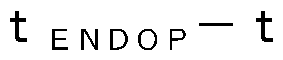 (1\/1) を表示部 2 1 0に表示させる (ステップ 3 6 2 7) 。 ステ ップ3 6 2 7では、 例えば、 判定部 1 9 5は、 通信部 1 9 6を介して、
 巳 〇 、 巳 し。— (IV!) 、 及び、 巳 〇 — (IV!) を表/」、装置 2
0 0に送信する。 例えば、 表示装置 2 0 0が備える制御部 2 4 0は、 処理部 1 9 0から 巳 し。、 巳 〇 、 巳 し。 _ (IV!) 、 及び、 巳 〇 _ ^ (
IV!) を、 通信部 2 2 0を介して受信した場合、 表示部 2 1 0を制御すること で、 表 部 2 1 0に 巳 し。、 巳 〇 、
 (IV!) 、 及び、 1 ^ ^〇 〇1= _ 1 (1\/1) を示す画像を表示させる。
[0172] また、 判定部 1 9 5は、
 (IV!) 、 及び、
 (IV!) を外部機器 3 0 0に通知する (ステップ 3 6 2 8) 。 ステ ップ3 6 2 8では、 例えば、 判定部 1 9 5は、 通信部 1 9 6を介して、
 巳 〇 、 巳 し。— (IV!) 、 及び、 巳 〇 — (IV!) を外部機器 3 0〇に送信する。
[0173] 図 1 2は、 実施の形態 1 に係る光源装置 1 〇〇が備える半導体レーザ素子
1 2 0の累積使用時間 1に対するしきい値電流 I 〇の値の増加の一例を示す グラフである。 図 1 3は、 実施の形態 1 に係る光源装置 1 0 0が備える半導 体レーザ素子 1 2 0の累積使用時間 1に対するスロープ効率 3 6の低下の一例 を示すグラフである。 例えば、 図 1 2は、 番号 nの半導体レーザ素子 1 2 0 を駆動させた場合のデータである。
〇 2020/175214 32 卩(:171? 2020 /006076
[0174] 判定部 1 9 5は、 図 1 2に示すように、 上記式 ( 1 ) を用いて、 例えば、 検査番号
 のしきい値電流 丨 (1^— 1^ ) と、 最新の検査番号 IV!のし きい値電流 I 〇 (IV!) の差分と、 基準しきい値電流 I
 とから半導体レーザ 素子 1 2 0の寿命 I ^ 0し0を算出する。 また、 判定部 1 9 5は、 算出した寿命 から、 半導体レーザ素子 1 2 0が寿命に到達していない場合、 寿命に 到達するまでの時間 (つまり、 故障と判定されるまでの時間) である

を算出する。
[0175] また、 判定部 1 9 5は、 図 1 3に示すように、 上記式 (2) を用いて、 例 えば、 検査番号 IV!—
 のスロープ効率 3 6 (IV!—
 と、 最新の検査番号 IV! のスロープ効率 3 6 (IV!) の差分と、 基準スロープ効率 3
 とから 1·!番目の 半導体レーザ素子
 を算出 する。 また、 判定部 1 9 5は、 算出した寿命 I
 から、 n番目の半導体レ
—ザ素子 1 2 0の後段に位置する寿命に到達していない場合、 寿命に到達す るまでの時間 (つまり、 故障と判定されるまでの時間) である
 - · I ( IV!) を算出する。
[0176] 図 1 2および図 1 3に示した例では、 半導体レーザ素子 1 2 0と第 1光学 素子 1 3 1 とは、 どちらも劣化が進んでいる。 累積使用時間 1が約 1 , 0 0 0時間の時点で第 1光学素子 1 3 1 が半導体レーザ素子 1 2 0よりもさきに 故障と判定される見込みとなる。 さらに、 半導体レーザ素子 1 2 0も累積使 用時間 1が約 1 , 7 0 0時間の時点で故障と判定される見込みとなる。 もし も、 第 1光学素子 1 3 1 の劣化がまったくなければ、 劣化するのは半導体レ —ザ素子 1 2 0のみである。 その場合、 図 1 3に示したスロープ効率 が基 準スロープ効率 3
 に到達する時間も約 1 , 7 0 0時間となるはずである。 つまり、 半導体レ—ザ素子】 2 0の寿命到達時点で、 しきい値電流 I 〇とス 口ープ効率 3 6とは、 それぞれ基準しきい値電流 丨 £ N 0と基準スロープ効率 3巳 。【' 到達すること(しなる。
[0177] 図 1 4は、 実施の形態 1 に係る光源装置 1 0 0の一例において、 第 1光学 素子 1 3 1 の劣化箇所 6 0 0を説明するための概略図である。 なお、 図 1 4
〇 2020/175214 33 卩(:171? 2020 /006076
に示す半導体レーザ素子 1 2 1、 1 2 2、 1 2 3、 1 2 4は、 それぞれ、 図 1 に示す半導体レーザ素子 1 2 0の一例である。 また、 図 1 4においては、 コリメータレンズ 1 3 1 3が有する複数のコリメータレンズのうち、 半導体 レーザ素子 1 2 2の後段に位置するコリメータレンズをコリメータレンズ 1 3 1 3と呼称している。 また、 図 1 4においては、 コリメータレンズ 1 3 1 匕が有する複数のコリメータレンズのうち、 半導体レーザ素子 1 2 2の後 段に位置するコリメータレンズをコリメータレンズ 1 3 1 匕匕と呼称してい る。
[0178] 例えば、 判定部 1 9 5は、 半導体レーザ素子 1 2 2を駆動させた場合のし きい値電流丨 〇及びスロープ効率 の結果から、 半導体レーザ素子 1 2 2の 後段に位置する第 1光学素子 1 3 1が故障していると判定したとする。 この 場合、 判定部 1 9 5は、 光学系 1 3 0に含まれ、 それぞれが第 1光学素子 1 3 1の一例である、 コリメータレンズ 1 3 1 3 3 , コリメータレンズ 1 3 1 匕匕、 及び、 集光レンズ 1 3 1 〇における半導体レーザ素子 1 2 2の後段に 位置する箇所 (つまり、 半導体レーザ素子 1 2 2が出力したレーザ光が通過 する箇所) を含む劣化箇所 6 0 0、 光ファイバ 1 3 1 、 コリメータレンズ 1 3 1 †, 並びに、 集光レンズ 1 3 1 9のいずれかが故障したことが分かる
[0179] [効果等]
以上説明したように、 実施の形態 1 に係る光源装置 1 〇〇は、 半導体レー ザ素子 1 2 0と、 半導体レーザ素子 1 2 0からの出射光 5 0 0を伝播する第 1光学素子 1 3 1 を有する光学系 1 3 0と、 第 1光学素子 1 3 1の少なくと も一部を伝播した第 1伝播光 5 1 0 3を受光する第 1受光部 1 4 0と、 半導 体レーザ素子 1 2 0の駆動電流を制御するレーザ駆動制御部 1 9 2 3と、 第 1受光部 1 4 0において受光された第 1伝播光 5 1 0 3の受光強度を示す第 1出力値を測定する測定回路 1 8 0と、 を備える。 第 1受光部 1 4 0は、 第 1光学素子 1 3 1の後段に配置される。 レーザ駆動制御部 1 9 2 3は、 互い に異なる複数の駆動電流で半導体レーザ素子 1 2 0を駆動させる。 測定回路
〇 2020/175214 34 卩(:171? 2020 /006076
1 8 0は、 互いに異なる複数の駆動電流の値に対する第 1受光部 1 4 0にお いて受光された第 1伝播光 5 1 0 3のそれぞれの第 1出力値を測定する。
[0180] このような構成によれば、 少なくとも 2つの駆動電流と、 当該 2つの駆動 電流に対応した光出力とから、 しきい値電流丨 〇と、 スロープ効率 とが算 出され得る。 そのため、 例えば、 算出されたしきい値電流丨 〇とスロープ効
 と基準スロープ効率
 とが予め任 意に定められていれば、 図 1 0に示すグラフを用いることで、 光学系 1 3 0 (具体的には、 第 1光学素子 1 3 1) の劣化度合いと、 半導体レーザ素子 1 2 0の劣化度合いとをそれぞれ判定できる。 そのため、 光源装置 1 0 0によ れば、 光源装置 1 〇〇から出力される光出力の低下が、 第 1受光部 1 4 0の 前段に位置する光学系 1 3 0 (具体的には、 第 1光学素子 1 3 1) の劣化に よる光出力の変化か半導体レーザ素子 1 2 0の劣化による光出力の変化かを 判別することができる。
[0181 ] また、 例えば、 第 1受光部 1 4 0は、 光学系 1 3 0の後段に配置される。
[0182] このような構成によれば、 例えば、 光学系 1 3 0が複数の第 1光学素子 1
3 1 を有する場合、 半導体レーザ素子 1 2 0と第 1受光部 1 4 0との間にあ る光学系 1 3 0が有する第 1光学素子 1 3 1の全ての劣化度合いと、 半導体 レーザ素子 1 2 0の劣化度合いとを判別することができる。
[0183] また、 例えば、 第 1光学素子 1 3 1は、 レンズ、 ミラー、 及び、 光導波路 の少なくともいずれかを含む。
[0184] つまり、 第 1光学素子 1 3 1は、 半導体レーザ素子 1 2 0から出射された レーザ光の配光の制御、 合波、 導波等ができる素子であればよい。 光源装置 1 0 0は、 このような第 1光学素子 1 3 1の劣化による光出力の変化か半導 体レーザ素子 1 2 0の劣化による光出力の変化かを判別することができる。
[0185] また、 例えば、 第 1受光部 1 4 0は、 第 1受光部 1 4 0の受光面において 、 第 1光学素子 1 3 1 によって出射光 5 0 0が集光された第 1伝播光 5 1 0 3を、 第 1伝播光 5 1 0 3の焦点からずれた位置で受光する。
[0186] このような構成によれば、 第 1受光部 1 4 0の受光面において、 極端にレ
〇 2020/175214 35 卩(:171? 2020 /006076
—ザ光が集中する箇所をなくすことができる。 そのため、 第 1受光部 1 4 0 が故障しにくくなる。
[0187] また、 例えば、 第 1受光部 1 4 0が受光する第 1伝播光 5 1 0 3に対応す る駆動電流は、 定格駆動電流よりも小さい。
[0188] 例えば、 しきい値電流 と、 スロープ効率 とを算出するためには、 半 導体レーザ素子 1 2 0がレーザ発振していればよく、 高い光出力は必要ない 。 そのため、 このような構成によれば、 第 1受光部 1 4 0に、 高い光出力の レーザ光が照射されることが抑制され得る。 そのため、 第 1受光部 1 4 0が さらに故障しにくくなる。
[0189] また、 例えば、 光源装置 1 0 0は、 さらに、 半導体レーザ素子 1 2 0の温 度を調整する温度調整部 1 5 0を備える。 また、 光源装置 1 0 0は、 さらに 、 温度調整部 1 5 0を制御する温度調整制御部 1 9 2 13を備える。 この場合 、 温度調整制御部 1 9 2 3は、 温度調整部 1 5 0を制御することで、 半導体 レーザ素子 1 2 0の温度を制御する。 例えば、 測定回路 1 8 0が第 1出力値 を測定するとき、 半導体レーザ素子 1 2 0の温度は、 温度調整制御部 1 9 2 13によって温度調整部 1 5 0が制御されることで、 予め定められた温度であ る基準温度の ± 5 °〇の範囲内に制御される。
[0190] スロープ効率 3 6には、 温度依存性があることが知られている。 そのため、 このような構成によれば、 半導体レーザ素子 1 2 0の温度を基準温度に近い 値にすることができる。 これにより、 スロープ効率 3 6は、 さらに精度よく算 出され得る。
[0191 ] また、 例えば、 光源装置 1 0 0は、 さらに、 第 1光学素子 1 3 1の劣化度 合いを判定する判定部 1 9 5を備える。 判定部 1 9 5は、 例えば、 互いに異 なる複数の駆動電流の値と、 互いに異なる複数の駆動電流の値に対する第 1 受光部 1 4 0において受光された第 1伝播光 5 1 0 3のそれぞれの第 1出力 値とに基づいて、 第 1光学素子 1 3 1の劣化度合いを判定する。 つまり、 半 0 定部 1 9 5は、 解析部 1 9 3が算出したしきい値電流丨 1 とスロープ効率 3 6 とから、 第 1光学素子 1 3 1の劣化度合いを判定する。
〇 2020/175214 36 卩(:171? 2020 /006076
[0192] このような構成によれば、 例えば、 第 1光学素子 1 3 1の劣化度合いの判 定を外部機器 3 0 0等にさせることなく、 光源装置 1 0 0が備える判定部 1 9 5によって、 第 1光学素子 1 3 1の劣化度合いを判定できる。
[0193] また、 例えば、 互いに異なる複数の駆動電流のうちの 2つの駆動電流の変 化量を△ 丨 チとし、 2つの駆動電流に対する第 1受光部 1 4 0において受光 された第 1伝播光 5 1 0 3のそれぞれの第 1出力値の変化量を△ 〇 とし た場合に、 判定部 1 9 5は、
 干 (つまり、 スロープ効率 3〇 に基づいて第 1光学素子 1 3 1の劣化度合いを判定する。
[0194] このような構成によれば、 判定部 1 9 5は、 スロープ効率 3 6から第 1光学 素子 1 3 1の劣化度合いを判定できる。
[0195] また、 例えば、 判定部 1 9 5は、 半導体レーザ素子 1 2 0がレーザ発振す るしきい値電流丨 〇の値の時間に対する変化量を算出し、 算出したしきい値 電流丨 〇の値の変化量を用いて、 半導体レーザ素子 1 2 0の寿命
 を 算出し、 且つ、 第 1光学素子 1 3 1の劣化度合いを判定する。
[0196] このような構成によれば、 判定部 1 9 5は、 半導体レーザ素子 1 2 0の劣 化度合いと区別して、 しきい値電流丨 〇の値の変化量から第 1光学素子 1 3 1の劣化度合いを判定できる。
[0197] また、 例えば、 判定部 1 9 5において、 第 1光学素子 1 3 1 を伝播した第
1伝播光 5 1 0 3を第 1受光部 1 4 0に受光させることで、 第 1光学素子 1 3 1の劣化度合いの判定と、 半導体レーザ素子 1 2 0の寿命の算出とを行う 検査モードと、 第 1光学素子 1 3 1 を伝播した第 1伝播光 5 1 0匕を照射対 象物 4 1 0に照射させる動作モードとを、 繰り返し行う。
[0198] このような構成によれば、 判定部 1 9 5は、 例えば、 照射対象物 4 1 0に レーザ光を照射していない時間帯を利用して、 半導体レーザ素子 1 2 0の劣 化度合いと第 1光学素子 1 3 1の劣化度合いとを判定できる。
[0199] また、 例えば、 判定部 1 9 5は、 算出した半導体レーザ素子 1 2 0の寿命 を外部機器 3 0 0に送信する。
[0200] このような構成によれば、 外部機器 3 0 0を使用する、 光源装置 1 0 0を
〇 2020/175214 37 卩(:171? 2020 /006076
メンテナンスするユーザに対して、 光源装置 1 0 0の半導体レーザ素子 1 2 0をメンテナンスする必要があるか否かを通知できる。 また、 例えば、 当該 ユーザは、 半導体レーザ素子 1 2 0の寿命から、 いつ半導体レーザ素子 1 2 〇をメンテナンスする必要があるかが分かる。
[0201 ] また、 例えば、 判定部 1 9 5は、 判定した第 1光学素子 1 3 1の劣化度合 いを外部機器 3 0 0に送信する。
[0202] このような構成によれば、 外部機器 3 0 0を使用する、 光源装置 1 0 0を メンテナンスするユーザに対して、 光源装置 1 0 0の第1光学素子 1 3 1 を メンテナンスする必要があるか否かを通知できる。
[0203] また、 例えば、 互いに異なる複数の駆動電流のうちの 2つの駆動電流の変 化量を△ 丨 チとし、 2つの駆動電流に対する第 1受光部 1 4 0において受光 された第

とした場合、 判定部 1 9 5は、
 干に基づいて、 第 1光学素子
1 3 1が故障と判定されるまでの累積使用時間 1、 及び、 第 1光学素子 1 3 1が故障と判定されるまでにかかる時間の少なくとも一方を算出する。
[0204] このような構成によれば、 例えば、 外部機器 3 0 0に光源装置 1 0 0をメ ンテナンスするユーザに対して、 第 1光学素子 1 3 1が故障と判定されるま での累積使用時間 1、 及び、 第 1光学素子 1 3 1が故障と判定されるまでに かかる時間を通知することで、 外部機器 3 0 0を使用する当該ユーザは、 光 源装置 1 〇〇のメンテナンスする必要がある時期が分かる。 そのため、 当該 ユーザは、 例えば、 光源装置 1 0 0をメンテナンスするスケジユールを光源 装置 1 0 0の光出力が著しく低下する前に決定しやすくなる。
[0205] また、 例えば、 判定部 1 9 5は、 算出した第 1光学素子 1 3 1が故障と判 定されるまでにかかる時間を外部機器 3 0 0に送信する。
[0206] このような構成によれば、 外部機器 3 0 0を使用する、 光源装置 1 0 0を メンテナンスするユーザは、 光源装置 1 〇〇の第 1光学素子 1 3 1 をメンテ ナンスすべき時期が分かる。
[0207] また、 例えば、 光源装置 1 0 0は、 半導体レーザ素子 1 2 0を複数備える
〇 2020/175214 38 卩(:171? 2020 /006076
。 この場合、 例えば、 レーザ駆動制御部 1 9 2 3は、 複数の半導体レーザ素 子 1 2 0をそれぞれ互いに異なるタイミングで駆動させる。 また、 例えば、 第 1受光部 1 4 0は、 それぞれ互いに異なるタイミングで駆動された複数の 半導体レーザ素子 1 2 0のそれぞれに対する第 1伝播光 5 1 0 3の少なくと も一部をそれぞれ受光する。 測定回路 1 8 0は、 複数の半導体レーザ素子 1 2 0のそれぞれについて、 互いに異なる駆動電流の値に対する第 1受光部 1 4 0において受光された第 1伝播光 5 1 0 3のそれぞれの第 1出力値を測定 する。
[0208] このような構成によれば、 判定部 1 9 5は、 複数の半導体レーザ素子 1 2
0それぞれの劣化度合いと、 複数の半導体レーザ素子 1 2 0それぞれの後段 に位置する第 1光学素子 1 3 1の劣化度合いを区別して判定できる。
[0209] また、 例えば、 半導体レーザ素子 1 2 0は、 窒化物半導体で構成される。
窒化物半導体の半導体レーザ素子 1 2 0は劣化しやすいため、 その劣化度合 いを判定できることは実用上有効である。
[0210] また、 例えば、 出射光 5 0 0の波長は、
 以下である。
[021 1 ] 光学系 1 3 0は、 特に、 出射光 5 0 0の波長が短い場合 (つまり、 1個の 光子のエネルギーが大きい場合) に、 劣化しやすい。 そのため、 出射光 5 0 0の波長が 5 0 0 n 以下であるような、 低波長の光を半導体レーザ素子 1 2 0が出射する場合に、 特に、 本開示に係る光源装置 1 〇〇が実行する光学 系 1 3 0の劣化による光出力の変化か半導体レーザ素子 1 2 0の劣化による 光出力の変化かを判別することが有効である。
[0212] (実施の形態 2)
続いて、 実施の形態 2に係る光源装置について説明する。 なお、 実施の形 態 2に係る光源装置の説明においては、 実施の形態 1 に係る光源装置 1 0 0 との差異点を中心に説明し、 実施の形態 1 に係る光源装置 1 0 0と同様の構 成については同様の符号を付し、 説明を省略又は簡略化する場合がある。
[0213] [構成]
まず、 図 1 5〜図 1 7を参照して、 実施の形態 2に係る光源装置の構成に
〇 2020/175214 39 卩(:171? 2020 /006076
ついて説明する。
[0214] 図 1 5は、 実施の形態 2に係る光源装置 1 0 0 3の特徴的な機能構成を示 すブロック図である。 図 1 6は、 実施の形態 2に係る光源装置 1 0〇 3が備 える光学モジュール部 1 1 0 3の詳細を説明するためのブロック図である。 図 1 7は、 実施の形態 2に係る光源装置 1 0 0 3の一例を模式的に示す概略 図である。
[0215] 光源装置 1 0 0 8は、 レーザ光を出力する装置である。 光源装置 1 0 0 8 は、 例えば、 図 1 7に示す照射対象物 4 1 0をレーザ光によって加工するレ —ザ加工機に用いられる。 なお、 図 1 7には、 一例として、 光源装置 1 0 0 3が複数の発光点を有する、 つまり、 複数の箇所から同じ方向にレーザ光を 出力する半導体レーザ素子 (半導体レ—ザアレイ素子) 】 2 5を 1つ備える 場合を例示している。 本実施の形態では、 半導体レーザ素子 1 2 5は、 4つ の発光点を有する。 もちろん、 半導体レーザ素子 1 2 5が有する発光点の数 は、 特に限定されない。
[0216] 図 1 5に示すように、 光源装置 1 0 0 3は、 光学モジュール部 1

、 回路部 1 6 0 3と、 処理部 1 9 0 3と、 を備える。
[0217] 光学モジュール部 1 1
 は、 レーザ光を出力する光源部である。 光学モ ジュール部 1 1 0は、 半導体レーザ素子 1 2 5と、 光学系 1 3 0 3と、 第 1 受光部 1 4 0と、 第 2受光部 1 4 1 と、 温度調整部 1 5 0と、 ステージ 4 2 〇と、 を備える。
[0218] 半導体レーザ素子 1 2 5は、 レーザ光を出力する半導体素子である。 半導 体レーザ素子 1 2 5が有する発光点の数は、 1以上であればよく、 特に限定 されない。 本実施の形態では、 光学モジュール部 1 1
 は、 1\1個の発光点 を有する半導体レーザ素子 1 2 5を 1つ備える。 なお、 図 1 7には、 一例と して、 半導体レ—ザ素子 1 2 5が発光点を 4つ備える場合を示している。 ま た、 複数の発光点は、 それぞれ独立して駆動可能なように、 駆動回路 1 7 0 と接続されている。
[0219] 半導体レーザ素子 1 2 5が出力するレーザ光 (出射光) の波長は、 例えば
\¥0 2020/175214 40 卩(:17 2020 /006076
、 5 0 0 n m以下である。 半導体レーザ素子 1 2 5は、 例えば、 窒化物半導 体で構成される。
[0220] 半導体レーザ素子 1 2 5は、 光学系 1 3 0 8へ向けてレーザ光を出力する
[0221 ] 光学系 1 3 0 3は、 半導体レーザ素子 1 2 5から出力されたレーザ光の配 光を制御する。 具体的には、 光学系 1 3 0 3は、 半導体レーザ素子 1 2 5か ら出力されたレーザ光のコリメート、 合波、 集光等を行い、 照射対象物 4 1 0又は第 1受光部 1 4 0に向けて配光を制御したレーザ光を出力する。
[0222] 光学系 1 3 0 3は、 第 1光学素子 1 3 1 と、 第 2光学素子 1 3 2と、 を備 える。 具体的には、 光学系 1 3 0 3は、 第 1光学素子 1 3 1の前段に第 2光 学素子 1 3 2を有する。
[0223] 第 2光学素子 1 3 2は、 半導体レーザ素子 1 2 5からの出射光 5 0 0を伝 播する。 第 2光学素子 1 3 2は、 例えば、 半導体レーザ素子 1 2 5から出力 されたレーザ光の配光の制御、 伝播等を制御する。 第 2光学素子 1 3 2は、 レンズ、 ミラー、 及び、 光導波路の少なくとも 1つを含む。 図 1 7には、 第 2光学素子 1 3 2の一例として、 コリメータレンズ 1 3 2 3、 1 3 2匕、 及 び、 集光レンズ 1 3 2〇を示している。
[0224] なお、 図 1 7に示すように、 コリメータレンズ 1 3 2 3、 1 3 2匕の各々 は、 レンズアレイとして、 一体的に形成されている。 このように、 光学系 1 3 0 3に採用される第 1光学素子 1 3 1及び第 2光学素子 1 3 2の形状は、 任意でよい。
[0225] 第 2光学素子 1 3 2は、 第 1光学素子 1 3 1 に向けて第 2伝播光 5 2 0を 出射する。
[0226] 第 1光学素子 1 3 1は、 第 2伝播光 5 2 0を伝播して、 第 1伝播光 5 1 0
3を第 1受光部 1 4 0に、 第 1伝播光 5 1 0匕を照射対象物 4 1 0に向けて 出射する。
[0227] 第 2受光部 1 4 1は、 第 2光学素子 1 3 2の少なくとも一部を伝播した第
2伝播光 5 2 0を受光する光センサである。 図 1 6に示すように、 第 2受光
〇 2020/175214 41 卩(:171? 2020 /006076
部 1 4 1は、 第 1光学素子 1 3 1 に向けて第 2光学素子 1 3 2から出射され た第 2伝播光 5 2 0の一部を検出する。 このように、 第 2受光部 1 4 1は、 第 2光学素子 1 3 2を伝播した第 2伝播光 5 2 0であって、 第 1光学素子 1 3 1 に入射する前の伝播光である第 2伝播光 5 2 0を受光する。 第 2受光部 1 4 1は、 回路部 1 6 0 3と制御線で接続されており、 検出した出力値 (ア ナログ値) を回路部 1 6〇 3に出力する。 具体的には、 第 2受光部 1 4 1は 、 回路部 1 6〇 3が有する測定回路 (受光強度測定部) 1 8 1 と制御線で接 続されており、 検出した出力値を測定回路 1 8 1 に出力する。
[0228] 第 1受光部 1 4 0は、 光学系 1 3 0 3 (具体的には、 第 1光学素子 1 3 1 及び第 2光学素子 1 3 2) の少なくとも一部を伝播した第 1伝播光 5 1 0 3 を受光する光センサである。
[0229] 温度調整部 1 5 0は、 半導体レーザ素子 1 2 5の温度を制御するための変 温器である。 半導体レーザ素子 1 2 5は、 例えば、 ペルチェ素子等の温度調 整部 1 5 0に搭載されている。
[0230] 回路部 1 6 0 3は、 処理部 1 9 0 3及び光学モジュール部 1 1 0 3と接続 されており、 処理部 1 9 0 3からの指示に基づいて、 光学モジュール部 1 1 0 3の動作を制御する。 回路部 1 6 0 3は、 例えば、 アナログ回路であり、 機能的には、 駆動回路 1 7 0と、 測定回路 1 8 0と、 測定回路 1 8 1 と、 を 備える。
[0231 ] 駆動回路 1 7 0は、 半導体レーザ素子 1 2 5を駆動するための回路である 。 本実施の形態では、 回路部 1 6 0は、 半導体レーザ素子 1 2 5が有する複 数の発光点をそれぞれ独立して光出力させることができるように、 半導体レ —ザ素子 1 2 5の発光点の数と同じ数だけの駆動回路 1 7 0を備える。 例え ば、 光学モジュール部 1 1 〇 3が1\1個の発光点を有する半導体レーザ素子 1 2 5を有する場合、 回路部 1 6 0は、 1\1個の駆動回路 1 7 0を有する。
[0232] 測定回路 1 8 1は、 第 2受光部 1 4 1 において受光された第 2伝播光 5 2 〇の受光強度を示す第 2出力値を測定する。 具体的には、 測定回路 1 8 1は 、 第 2受光部 1 4 1から出力されたアナログの出力値をデジタルの出力値に
\¥0 2020/175214 42 卩(:17 2020 /006076
変換する 変換器である。 測定回路 1 8 1は、 第 2出力値を処理部 1 9〇 3 (より具体的には、 処理部 1 9 0 8が有する解析部 1 9 3 8) に出力する
[0233] 処理部 1 9 0 3は、 回路部 1 6 0 3の動作を制御する。 具体的には、 処理 部 1 9 0 3は、 回路部 1 6 0 3を制御することで、 半導体レーザ素子 1 2 5 の駆動電流を制御する。
[0234] 処理部 1 9 0 3は、 機能的には、 設定部 1 9 1 と、 制御部 1 9 2と、 解析 部 1 9 3 3と、 記憶部 1 9 4 3と、 判定部 (劣化判定部) 1 9 5 3と、 通信 部 1 9 6と、 を備える。
[0235] 設定部 1 9 1は、 半導体レーザ素子 1 2 5の駆動電流の値を設定する。 例 えば、 設定部 1 9 1は、 ユーザが操作する表示装置 2 0 0から半導体レーザ 素子 1 2 5の駆動電流の値を示す情報を取得し、 取得した駆動電流の値を記 憶部 1 9 4 3に記憶させる。 また、 設定部 1 9 1は、 光学モジュール部 1 1 〇 3が複数の発光点を有する半導体レーザ素子 1 2 5を有する場合、 使用す る半導体レーザ素子 1 2 5における発光点を選択する。 例えば、 設定部 1 9 1は、 ユーザが操作する表示装置 2 0 0から使用する半導体レーザ素子 1 2 5の発光点を示す情報を取得し、 取得した使用する半導体レーザ素子 1 2 5 の発光点を示す情報を記憶部 1 9 4 3に記憶させる。 なお、 設定部 1 9 1は 、 通信インターフェースを有し、 表示装置 2 0 0と通信可能に接続されてい てもよいし、 通信部 1 9 6を介して表示装置 2 0 0と通信してもよい。
[0236] 制御部 1 9 2は、 半導体レーザ素子 1 2 5の駆動電流を制御するレーザ駆 動制御部 1 9 2 3と、 温度調整部を制御する温度調整制御部 1 9 2 と、 半 導体レーザ素子 1 2 0を保持するステージの駆動を制御するステージ制御部 と 1 9 2〇を備える。 具体的には、 制御部 1 9 2のレーザ駆動制御部 1 9 2 3は、 回路部 1 6〇 3が有する駆動回路 1 7 0を制御することで、 設定部 1 9 1が設定した使用する半導体レーザ素子 1 2 5の発光点に、 設定部 1 9 1 が設定した駆動電流の値だけ電流に印加させて、 半導体レーザ素子 1 2 5の 任意の発光点を駆動させる。 レーザ駆動制御部 1 9 2 3は、 例えば、 検査モ
〇 2020/175214 43 卩(:171? 2020 /006076
-ドにおいては、 互いに異なる複数の駆動電流で半導体レーザ素子 1 2 5の 複数の発光点を 1つずつ駆動させる。 この場合、 測定回路 1 8 0は、 互いに 異なる複数の駆動電流の値に対する第 1受光部 1 4 0において受光された第 1伝播光 5 1 0 3のそれぞれの第 1出力値を測定する。 また、 測定回路 1 8 1は、 互いに異なる複数の駆動電流の値に対する、 第 2受光部 1 4 1 におい て受光された第 2伝播光 5 2 0の受光強度を示す第 2出力値をそれぞれ測定 する。
[0237] 解析部 1 9 3 3は、 測定回路 1 8 0、 1 8 1から取得した半導体レーザ素 子 1 2 5のレーザ光の出力値に基づいて、 しきい値電流丨 〇と、 スロープ効 率 3 ^、
 とを算出する。
[0238] スロープ効率 3 は、 レーザ光を発振する電流の値における、 電流の値に 対する第 1受光部 1 4 0で受光されたレーザ光の光出力の変化量 (つまり、 傾き) である。
[0239] また、 スロープ効率 3 は、 レーザ光を発振する電流の値における、 電流 の値に対する第 2受光部 1 4 1で受光されたレーザ光の光出力の変化量 (つ まり、 傾き) である。
[0240] このように、 解析部 1 9 3 3は、 第 1受光部 1 4 0及び第 2受光部 1 4 1 のそれぞれで検出されたレーザ光に対するスロープ効率 3 6 1 , 3 6 2を算出す る。
[0241 ] 記憶部 1 9 4 3は、 解析部 1 9 3 3が算出したしきい値電流丨 1 と、 スロ —プ効率 3 6 1 % 3 とを記憶する。
[0242] 記憶部 1 9 4 3は、 例えば、 !! 0 0、 不揮発性メモリ等である。
[0243] 判定部 1 9 5 3は、 解析部 1 9 3 3が算出した、 しきい値電流丨 1 とスロ
 とから、 半導体レーザ素子 1 2 5及び光学系 1 3〇 3の 劣化度合いを判定する。 具体的には、 判定部 1 9 5 3は、 しきい値電流丨 〇 から半導体レーザ素子 1 2 5の劣化度合いを判定し、 スロープ効率 3 ^から 光学系 1 3 0 3が有する第 1光学素子 1 3 1の劣化度合いを判定し、 且つ、 スロープ効率 から光学系 1 3 0 3が有する第 2光学素子 1 3 2の劣化度
〇 2020/175214 44 卩(:171? 2020 /006076
とから、 半導体レーザ素子 1 2 5及び光学系 1 3〇 3の 劣化度合いを判定する。 具体的には、 判定部 1 9 5 3は、 しきい値電流丨 〇 から半導体レーザ素子 1 2 5の劣化度合いを判定し、 スロープ効率 3 ^から 光学系 1 3 0 3が有する第 1光学素子 1 3 1の劣化度合いを判定し、 且つ、 スロープ効率 から光学系 1 3 0 3が有する第 2光学素子 1 3 2の劣化度
〇 2020/175214 44 卩(:171? 2020 /006076
合いを判定する。
[0244] 具体的には、 判定部 1 9 5 3は、 駆動電流の複数の値と、 駆動電流の複数 の値に対応するそれぞれの出力とに基づいて、 第 1光学素子 1 3 1及び第 2 光学素子 1 3 2の劣化度合いを判定する。 より具体的には、 判定部 1 9 5 3 は、 互いに異なる複数の駆動電流の値と、 互いに異なる複数の駆動電流の値 に対する第 1受光部 1 4 0において受光された第 1伝播光 5 1 0 3のそれぞ れの第 1出力値とに基づいて、 第 1光学素子 1 3 1の劣化度合いを判定し、 且つ、 互いに異なる複数の駆動電流の値と、 互いに異なる複数の駆動電流の 値に対する第 2受光部 1 4 1 において受光された第 2伝播光 5 2 0のそれぞ れの第 2出力値とに基づいて、 第 2光学素子 1 3 2の劣化度合いを判定する
[0245] 以上のように、 光源装置 1 0 0 3では、 実施の形態 1 に係る光源装置 1 0
0の処理に、 さらに、 第 2受光部 1 4 1で受光された第 2伝播光 5 2 0の光 出力に基づいて、 スロープ効率 3 を算出し、 算出したスロープ効率 3 に 基づいて、 第 2光学素子 1 3 2の劣化度合いを算出する。 他の構成要素及び 処理に関しては、 光源装置 1 0 0 3は、 実施の形態 1 に係る光源装置 1 0 0 と同様であるため、 説明を省略する。
[0246] 処理部 1 9 0 3は、 処理部 1 9 0と同様に、 例えば、 〇 IIと、 〇 IIが 実行する制御プログラムとによって実現される。 当該制御プログラムは、 例 えば、 記憶部 1 9 4 3に記憶されている。 なお、 処理部 1 9 0 3は、 専用の 電子回路等で実現されてもよい。 例えば、 設定部 1 9 1 と、 制御部 1 9 2と 、 解析部 1 9 3 3と、 判定部 1 9 5 3とは、 1つの〇 IIで実現されてもよ いし、 複数の〇 IIで実現されてもよい。
[0247] [処理手順]
続いて、 図 1 8〜図 2 8を参照しながら、 実施の形態 2に係る光源装置 1 0〇 3が実行する半導体レーザ素子 1 2 5と第 1光学素子 1 3 1 と第 2光学 素子 1 3 2の劣化度合いを判定する処理手順について説明する。
[0248] なお、 以下で説明する実施の形態 2に係る光源装置 1 0 0 3が実行する処
〇 2020/175214 45 卩(:171? 2020 /006076
理手順において、 実施の形態 1 に係る光源装置 1 〇〇が実行する処理手順と 実質的に同様のステップについては、 同様の符号を付し、 説明を省略又は簡 略化する場合がある。
[0249] 図 1 8は、 実施の形態 2に係る光源装置 1 0 0 3が実行する半導体レーザ 素子 1 2 5と第 1光学素子 1 3 1 と第 2光学素子 1 3 2との劣化度合いを判 定する処理手順を示すフローチヤートである。
[0250] まず、 光源装置 1 0 0 3は、 半導体レーザ素子 1 2 5、 第 1光学素子 1 3
1、 及び第 2光学素子 1 3 2の特性解析処理を実行する (ステップ 3 1 3)
。 具体的には、 ステップ 3 1 3では、 解析部 1 9 3 3は、 しきい値電流丨 〇 とスロープ効率 3 とスロープ効率 3 とを算出して、 記憶部 1 9 4 3に記 憶させる。
[0251 ] 次に、 光源装置 1 0 0 3は、 半導体レーザ素子 1 2 5、 第 1光学素子 1 3
1、 及び、 第 2光学素子 1 3 2の初期データ記憶処理を実行する (ステップ 3 2 3) 。 具体的には、 ステップ 3 2 3では、 解析部 1 9 3 3は、 第 1光学 素子 1 3 1から出力されたレーザ光からステップ 3 1 3で算出した、 しきい 値電流丨 〇とスロープ効率 とのそれぞれの初期値を算出し、 算出した初 期値に基づいて判定部 1 9 5 3による劣化度合いの判定の基準となる基準し きい値電流丨
 と、 基準スロープ効率 3
 とを算出して、 記憶部 1 9 4
3に記憶させる。 また、 解析部 1 9 3 3は、 第 2光学素子 1 3 2から出力さ れたレーザ光 (第 2伝播光 5 2 0) からステップ 3 1 3で算出した、 スロー プ効率 3 の初期値を算出し、 算出した初期値に基づいて判定部 1 9 5 3に よる劣化度合いの判定の基準となる基準スロープ効率 3
 とを算出して、 記憶部 1 9 4 3に記憶させる。
[0252] 基準スロープ効率
 と基準スロープ効率
 とは、 例えば、 それぞ れの初期値に対して予め定められた定数を乗算することで算出される。 なお 基準しきい値電流 I と、 基準スロープ効率
 と、 基準スロープ効
 に定められていてもよい。
[0253] 次に、 光源装置 1 0 0 3は、 動作モードで光学モジュール部 1
〇 2020/175214 46 卩(:171? 2020 /006076
用する (ステップ 3 3 3) 。 例えば、 ステップ 3 3 3は、 ステップ 3 3の処 理と同様である。
[0254] 次に、 光源装置 1 0 0 3は、 半導体レーザ素子 1 2 5、 第 1光学素子 1 3
1、 及び、 第 2光学素子 1 3 2の特性解析処理を実行する (ステップ 3 4 3 ) 。 具体的には、 ステップ 3 4 3では、 ステップ 3 1 3と同様に、 解析部 1 9 3 3は、 第 1光学素子 1 3 1から出力されたレーザ光から、 しきい値電流 I 〇とスロープ効率 3 とを算出し、 且つ、 第 2光学素子 1 3 2から出力さ れた第 2伝播光 5 2 0から、 スロープ効率 を算出する。
[0255] 次に、 光源装置 1 0 0 3は、 半導体レーザ素子 1 2 5、 第 1光学素子 1 3
1、 及び、 第 2光学素子 1 3 2のデータ記憶処理を実行する (ステップ 3 5 3) 。 具体的には、 ステップ 3 5 3では、 解析部 1 9 3 3は、 ステップ 3 4 3で算出した、 しきい値電流丨 〇とスロープ効率 とスロープ効率 と のそれぞれの値を、 半導体レーザ素子 1 2 5が利用された時間である累積使 用時間 1に紐づけて、 記憶部 1 9 4 3に記憶させる。
[0256] 次に、 光源装置 1 0 0 3は、 半導体レーザ素子 1 2 5、 第 1光学素子 1 3
1、 及び、 第 2光学素子 1 3 2の劣化判定処理を実行する (ステップ 3 6 3 ) 。 具体的には、 ステップ 3 6 3では、 判定部 1 9 5 3は、 ステップ 3 5 3 で解析部 1 9 3 3が記憶部 1 9 4 3に記憶させたしきい値電流丨 1 とスロー プ効率 3 6 !とスロープ効率 3 6 2と累積使用時間 1とから、 半導体レーザ素子 1 2 5、 第 1光学素子 1 3 1、 及び、 第 2光学素子 1 3 2の劣化度合いを判 定する。
[0257] 次に、 光源装置 1 0 0 3は、 光源装置 1 0 0 3の使用を終了するか否かを 判定する (ステップ 3 7 3) 。 例えば、 ステップ 3 7 3は、 ステップ 3 7の 処理と同様である。
[0258] 続いて、 図 1 8に示す各ステップの詳細について説明する。
[0259] なお、 以下で説明する図 1 9〜図 2 6のフローチヤートでは、 光源装置 1 〇〇 3が1\1個の発光点を有する半導体レーザ素子 1 2 5を備える場合を例示 して説明する。
〇 2020/175214 47 卩(:171? 2020 /006076
[0260] 図 1 9は、 実施の形態 2に係る光源装置 1 0 0 3が実行する特性解析処理 (具体的には、 ステップ 3 1 3及びステップ 3 4 3) の詳細を説明するため のフローチヤートである。 ステップ 3 1 3とステップ 3 4 3とは、 半導体レ —ザ素子 1 2 5の初期値であるどうかが異なるのみであり、 図 1 9では、 ス テップ3 1 8の詳細を説明する。
[0261 ] まず、 設定部 1 9 1は、 1\1個の半導体レーザ素子 1 2 5の中から 1つの半 導体レーザ素子 1 2 5を選択して設定する。 つまり、 設定部 1 9 1は、 1\1個 の半導体レーザ素子 1 2 5の発光点の中から 1つの半導体レーザ素子 1 2 5 の発光点を選択して設定する。
[0262] ここで、 例えば、 1\1個の半導体レーザ素子 1 2 5の発光点には、 1\1個の半 導体レーザ素子 1 2 5の発光点をそれぞれ区別できるように、 番号 1から番 号 1\!までの番号が予め割り振られている。 例えば、 設定部 1 9 1は、 1\1個の 半導体レーザ素子 1 2 5の発光点の中から番号 n = 1の半導体レーザ素子 1 2 5の発光点を選択して設定する (ステップ 3 1 0 1 3) 。
[0263] なお、 以下では、 番号门の半導体レーザ素子 1 2 5の発光点を、 単に、 番 号 nの半導体レーザ素子 1 2 5と記載する場合がある。
[0264] 次に、 制御部 1 9 2は、 ステップ 3 1 0 1 3で設定部 1 9 1が設定した番 号 n = 1の半導体レーザ素子 1 2 5を駆動 (つまり、 レーザ光を出力) させ る (ステップ3 1 0 2 3) 。
[0265] 次に、 解析部 1 9 3 3は、 第 2受光部 1 4 1での受光強度に基づく番号 n = 1の半導体レ—ザ素子】 2 5の I 特性 (駆動電流に対する光出力) を 計測する (ステップ 3 1 0 3 3) 。 具体的には、 解析部 1 9 3 3は、 測定回 路 1 8 1から第 2受光部 1 4 1が受光した番号 n = 1の半導体レーザ素子 1 2 5の光出力を取得して、 且つ、 制御部 1 9 2が番号 n = 1の半導体レーザ 素子 1 2 5を駆動させている駆動電流を取得する。
[0266] 次に、 解析部 1 9 3 3は、 ステップ 3 1 0 3 3で計測した番号 n = 1の半 導体レーザ素子 1 2 5の丨 特性から、 スロープ効率 3 を算出する (ス テップ 3 1 0 4 8) 。
〇 2020/175214 48 卩(:171? 2020 /006076
[0267] 次に、 解析部 1 9 3 3は、 ステップ 3 1 0 4 3で算出した番号 n = 1の半 導体レーザ素子 1 2 5のスロープ効率 3 を記憶部 1 9 4 3に記憶させる ( ステップ 3 1 0 5 3) 。
[0268] なお、 ステップ 3 1 0 5 3では、 例えば、 解析部 1 9 3 3は、 制御部 1 9
2によって計測されている半導体レーザ素子 1 2 5の累積使用時間 1をあわ せて記憶部 1 9 4 3に記憶させる。
[0269] 次に、 解析部 1 9 3 3は、 第 1受光部 1 4 0での受光強度に基づく番号 n = 1の半導体レ—ザ素子】 2 5の I 特性 (駆動電流に対する光出力) を 計測する (ステップ 3 1 0 3匕) 。 具体的には、 解析部 1 9 3 3は、 測定回 路 1 8 0から第 1受光部 1 4 0が受光した番号 n = 1の半導体レーザ素子 1 2 5の光出力を取得して、 且つ、 制御部 1 9 2が番号 n = 1の半導体レーザ 素子 1 2 5を駆動させている駆動電流を取得する。
[0270] 次に、 解析部 1 9 3 3は、 ステップ 3 1 0 3 3で計測した番号 n = 1の半 導体レーザ素子 1 2 5の I _ I -特性から、 しきい値電流丨 1 とスロープ効率 とを算出する (ステップ 3 1 0 4 1〇) 。
[0271 ] 次に、 解析部 1 9 3 3は、 ステップ 3 1 〇 4匕で算出した番号 n = 1の半 導体レ—ザ素子 1 2 5のしきい値電流丨 1 とスロープ効率 3 6〗とを記憶部 1 9 4 3に記憶させる (ステップ 3 1 0 5匕) 。
[0272] なお、 しきい値電流丨 〇は、 第 2受光部 1 4 1での受光強度に基づいて算 出されてもよい。
[0273] 次に、 設定部 1 9 1は、 番号 nの次の番号 4 + 1) の半導体レーザ素子
1 2 5を設定する (ステップ 3 1 0 6) 。
[0274] 次に、 制御部 1 9 2は、 ステップ3 1 0 6で設定部 1 9 1が設定した番号 nが n > Nを満たすか、 つまり、 光源装置 1 0 0 3が備える 1\1個の半導体レ —ザ素子 1 2 5に設定されている番号の最大値を超えるか否かを判定する ( ステップ 3 1 0 7) 。
[0275] 制御部 1 9 2は、 门> 1\1でないと判定した場合 (ステップ 3 1 0 7で 1\1〇 ) 、 処理をステップ3 1 0 2 3に戻す。
〇 2020/175214 49 卩(:171? 2020 /006076
[0276] —方、 制御部 1 9 2は、 ると判定した場合 (ステップ 3 1 0 7 で丫6 3) 、 1\1個の半導体レーザ素子 1 2 5のしきい値電流 I 〇とスロープ 効率 3 6 !とスロープ効率 3 6 2とを記憶部 1 9 4 3に記憶させたとして、 処理 を終了する。
[0277] 図 2 0は、 実施の形態 2に係る光源装置 1 0 0 3が実行する初期データ記 憶処理の詳細を説明するためのフローチヤートである。 具体的には、 図 2 0 は、 図 1 8に示すステップ 3 2 8の詳細を示すフローチヤートである。
[0278] まず、 設定部 1 9 1は、 図 1 8に示すステップ 3 1 3で解析部 1 9 3 3が 解析した 1\1個の半導体レーザ素子 1 2 5それぞれのしきい値電流 I 〇の初期 値とスロープ効率 3 とスロープ効率 3 の初期値とに IV! = 0と設定する ( ステップ 3 2 0 1 3) 。
[0279] 次に、 設定部 1 9 1は、 1\1個の半導体レーザ素子 1 2 5の中から番号 n =
1の半導体レーザ素子 1 2 5を選択して設定する (ステップ 3 2 0 2 3) 。
[0280] 次に、 解析部 1 9 3 3は、 ステップ 3 2 0 2 3で設定部 1 9 1が設定した 番号 n = 1の半導体レ—ザ素子】 2 5の累積使用時間 1を記憶部 1 9 4 3か ら取得する (ステップ 3 2 0 3 3) 。
[0281 ] 次に、 解析部 1 9 3 3は、 記憶部 1 9 4 3に記憶させている番号门 = 1の 半導体レーザ素子 1 2 5の丨 -特性を取得する (ステップ 3 2 0 4 3) 。 ステップ 3 2 0 4 3では、 解析部 1 9 3 3は、 記憶部 1 9 4 3に記憶させて いる番号 n = 1の半導体レーザ素子 1 2 5の第 1受光部 1 4 0での受光強度 に基づく 丨 特性と、 第 2受光部 1 4 1での受光強度に基づく 丨 特性 とを取得する。
[0282] 次に、 解析部 1 9 3 3は、 記憶部 1 9 4 3に記憶させている番号门 = 1の 半導体レーザ素子 1 2 5のしきい値電流 I 〇とスロープ効率 とスロープ 効率 とを取得する (ステップ 3 2 0 5 3) 。
[0283] 次に、 解析部 1 9 3 3は、 取得した番号 n = 1の半導体レ—ザ素子】 2 5 のしきい値電流丨 〇とスロープ効率 3 とスロープ効率 と累積使用時間 1と紐づけたデータテーブル 3 4 0 3 (図 2 2参照) を記憶部 1 9 4 3に記
〇 2020/175214 50 卩(:171? 2020 /006076
憶させる (ステップ 32063) 。
[0284] 次に、 解析部 1 933は、 ステップ 32063で記憶部 1 943に記憶さ せた初期データから、 番号门 = 1の半導体レーザ素子 1 25における、 判定 部 1 953が番号 n = 1の半導体レ—ザ素子 1 25、 第 1光学素子 1 3 1、 及び、 第 2光学素子 1 32の劣化度合いを判定するために用いる寿命判定基 準データである基準しきい値電流丨
 と基準スロープ効率 3
 と基準ス ープ効率 3 とを設定 (算出) して、 記憶部 1 943に記憶させる (ス

[0285] 次に、 設定部 1 9 1は、 番号 nの次の番号 4 + 1) の半導体レーザ素子
1 25を設定する (ステップ 3208) 。
[0286] 次に、 制御部 1 92は、 ステップ 3208で設定部 1 9 1が設定した番号 nが n>Nを満たすか、 つまり、 光源装置 1 003が備える 1\1個の半導体レ —ザ素子 1 25に設定されている番号の最大値を超えるか否かを判定する ( ステップ 3209) 。
[0287] 制御部 1 92は、 门>1\1でないと判定した場合 (ステップ 3209で 1\1〇 ) 、 処理をステップ 32038に戻す。
[0288] —方、 制御部 1 92は、 n>Nであると判定した場合 (ステップ 3209 で丫63) 、 1\!個の半導体レーザ素子 1 25のデータテーブル 3403、 3 4 1 3、 3423を記憶部 1 943に記憶させたとして、 処理を終了する。
[0289] 図 2 1は、 実施の形態 2に係る光源装置 1 003が実行するデータ記憶処 理 (ステップ 353) の詳細を説明するためのフローチヤートである。
[0290] まず、 設定部 1 9 1は、 1\1個の半導体レーザ素子 1 25の中から番号 n =
1の半導体レーザ素子 1 25を選択して設定する (ステップ 3501 3) 。
[0291] 次に、 解析部 1 933は、 検査番号 IV!を更新 (1\/1 = 1\/1+ 1) する (ステッ プ35023) 〇
[0292] 次に、 解析部 1 933は、 制御部 1 92から番号 n = 1の半導体レーザ素 子 1 25の累積使用時間 Iを取得する (ステップ35033) 。
[0293] 次に、 解析部 1 933は、 記憶部 1 943に記憶させている番号门 = 1の
〇 2020/175214 51 卩(:171? 2020 /006076
半導体レ—ザ素子 1 2 5の 2回目の測定結果であるしきい値電流丨 1 とスロ —プ効率 3 とスロープ効率 3 とを取得する (ステップ 3 5 0 4 3) 。
[0294] 次に、 解析部 1 9 3 3は、 取得した番号 n = 1の半導体レーザ素子 1 2 5 の 2回目の測定結果であるしきい値電流丨 1 とスロープ効率 3 6 !とスロープ 効率 と累積使用時間 1と紐づけたデータテーブル 3 4 1 3 (図 7参照) を記憶部 1 9 4 3に記憶させる (ステップ3 5 0 5 3) 。
[0295] なお、 2回目の測定結果は、 図 3に示すステップ 3 4 3で解析部 1 9 3 3 が記憶部 1 9 4 3に記憶させている。
[0296] 次に、 設定部 1 9 1は、 番号 nの次の番号 4 + 1) の半導体レーザ素子
1 2 5を設定する (ステップ 3 5 0 6) 。
[0297] 次に、 制御部 1 9 2は、 ステップ 3 2 0 8で設定部 1 9 1が設定した番号 nが n>Nを満たすか、 つまり、 光源装置 1 0 0 3が備える 1\1個の半導体レ —ザ素子 1 2 5に設定されている番号の最大値を超えるか否かを判定する ( ステップ 3 5 0 7) 。
[0298] 制御部 1 9 2は、 门>1\1でないと判定した場合 (ステップ 3 5 0 7で 1\1〇 ) 、 処理をステップ 3 5 0 2 8に戻す。
[0299] —方、 制御部 1 9 2は、 >1\1であると判定した場合 (ステップ 3 5 0 7 で丫6 3) 、 1\1個の半導体レーザ素子 1 2 5における検査番号 IV!のデータテ —ブル (例えば、 図 2 2に示すデータテーブル 3 4 0 3、 3 4 1 3、 3 4 2 a) を記憶部 1 9 4 3に記憶させたとして、 処理を終了する。
[0300] 図 2 2は、 実施の形態 2に係る光源装置 1 0 0 3が記憶するデータテーブ ル 3 4 0 8、
 3 4 2 3の一例を示す表である。
[0301 ] 図 2 2に示すように、 例えば、 データテーブル 3 4 0 3には、 番号 n = 1 の半導体レーザ素子 1 2 5の検査番号 IV! = 0から IV! = 1 2までの、 累積使用 時間 と、 しきい値電流丨 〇と、 スロープ効率 3 と、 スロープ効率 と が含まれている。
[0302] つまり、 例えば、 図 7に示すデータテーブル 3 4 0とは、 データテーブル
3 4 0 3は、 2つのスロープ効率 3 6 1、 3 を含んでいる点が異なる。
〇 2020/175214 52 卩(:171? 2020 /006076
[0303] 図 2 3は、 実施の形態 2に係る光源装置 1 0 0 3が実行する劣化判定処理 (ステップ3 6 3) の詳細を説明するためのフローチヤートである。
[0304] まず、 設定部 1 9 1は、 1\1個の半導体レーザ素子 1 2 5の中から番号 n =
1の半導体レーザ素子 1 2 5を選択して設定する (ステップ 3 6 0 3) 。
[0305] 次に、 判定部 1 9 5 3は、 番号 n = 1の半導体レーザ素子 1 2 5、 第 1光 学素子 1 3 1、 及び、 第 2光学素子 1 3 2の故障判定処理を実行する (ステ ップ 3 6 1 3) 。 具体的には、 ステップ 3 6 1 3では、 判定部 1 9 5 3は、 記憶部 1 9 4 3に記憶されたデータテーブルに基づいて、 番号 n = 1の半導 体レーザ素子 1 2 5、 第 1光学素子 1 3 1、 及び、 第 2光学素子 1 3 2が故 障しているか否かを判定する。
[0306] 次に、 判定部 1 9 5 3は、 番号 n = 1の半導体レーザ素子 1 2 5、 第 1光 学素子 1 3 1、 及び、 第 2光学素子 1 3 2の寿命予測処理を実行する (ステ ップ 3 6 2 3) 。 具体的には、 ステップ 3 6 2では、 判定部 1 9 5 3は、 記 憶部 1 9 4 3に記憶されたデータテーブルに基づいて、 番号 n = 1の半導体 レーザ素子 1 2 5、 第 1光学素子 1 3 1、 及び、 第 2光学素子 1 3 2の寿命 を算出する。
[0307] つまり、 判定部 1 9 5 3は、 ステップ 3 6 1 3及びステップ3 6 2 3では 、 番号 n = 1の半導体レ—ザ素子 1 2 5、 第 1光学素子 1 3 1、 及び、 第 2 光学素子 1 3 2の劣化度合いを算出する。
[0308] 次に、 設定部 1 9 1は、 番号 nの次の番号 4 + 1) の半導体レーザ素子
1 2 5を設定する (ステップ 3 6 3) 。
[0309] 次に、 判定部 1 9 5 3は、 ステップ 3 6 3で設定部 1 9 1が設定した番号 nが n > Nを満たすか、 つまり、 光源装置 1 0 0 3が備える 1\1個の半導体レ —ザ素子 1 2 5に設定されている番号の最大値を超えるか否かを判定する ( ステップ3 6 4) 。
[0310] 判定部 1 9 5 3は、 制御部 1 9 2が n > Nでないと判定した場合 (ステッ プ 3 6 4で 1\1〇) 、 処理をステップ 3 6 1 8に戻す。
[031 1 ] —方、 判定部 1 9 5 3は、 制御部 1 9 2が n > Nであると判定した場合 (
〇 2020/175214 53 卩(:171? 2020 /006076
ステップ 364で丫 6 3) 、 1\1個の半導体レーザ素子 1 25、 第 1光学素子 1 3 1、 及び、 第 2光学素子 1 32における劣化度合いの判定をしたとして 、 処理を終了する。
[0312] 図 24は、 実施の形態 2に係る光源装置 1 003が実行する故障判定処理 (ステップ 36 1 3) の詳細を説明するためのフローチヤートである。
[0313] まず、 判定部 1 953は、 記憶部 1 943から番号 nの半導体レーザ素子
1 25のしきい値電流丨 〇とスロープ効率
 とを取得する (ステッ プ36 1 1 3) 0
[0314] 次に、 判定部 1 953は、 番号 nの半導体レーザ素子 1 25の寿命判定基 準データである基準しきい値電流丨
 と基準スロープ効率 3
 と基準ス 口ープ効率
 とを取得する (ステップ 36 1 23) 。
[0315] 次に、 判定部 1 953は、 しきい値電流丨 〇<基準しきい値電流丨
 であ るか否かを判定する (ステップ 36 1 3) 。
[0316] 判定部 1 953は、 しきい値電流丨 〇<基準しきい値電流丨
 でないと判 定した場合 (ステップ 36 1 3で N 0) 、 番号 nの半導体レーザ素子 1 25 が寿命に到達したことを表示部 2 1 0に表示させる (ステップ 36 1 43)
[0317] なお、 判定部 1 953は、 図 9に示すステップ 36 1 5のように、 番号 n の半導体レーザ素子 1 25が寿命に到達したことを外部機器 300に通知し てもよい。
[0318] —方、 判定部 1 953は、 しきい値電流丨 〇<基準しきい値電流丨
 であ ると判定した場合 (ステップ 36 1 3で丫63) 、 スロープ効率 3 >基準 スロープ効率 3
 であるか否かを判定する (ステップ 36 1 63) 。
[0319] 判定部 1 953は、 スロープ効率 3 >基準スロープ効率
 でないと 判定した場合 (ステップ 36 1 63で1\1〇) 、 番号 nの半導体レーザ素子 1 25が出力したレーザ光が通過する第 2光学素子 1 32が寿命に到達したこ とを表示部 2 1 0に表示させる (ステップ 36 1 73) 。
[0320] なお、 判定部 1 953は、 図 9に示すステップ 36 1 8のように、 第 2光
〇 2020/175214 54 卩(:171? 2020 /006076 学素子 1 32が寿命に到達したことを外部機器 300に通知してもよい。
[0321] 判定部 1 953は、 スロープ効率 3 >基準スロープ効率
 であると 判定した場合 (ステップ 36 1 63で丫63) 、 スロープ効率
 基準ス 口ープ効率
 るか否かを判定する (ステップ 36 1 613) 。
[0322] 判定部 1 953は、 スロープ効率
 基準スロープ効率
 でないと 判定した場合 (ステップ 36 1 613で1\1〇) 、 番号 nの半導体レーザ素子 1
25が出力したレーザ光が通過する第 1光学素子 1 3 1が寿命に到達したこ とを表示部 2 1 0に表示させる (ステップ 36 1 7匕) 。
[0323] なお、 判定部 1 953は、 図 9に示すステップ 36 1 8のように、 第 1光 学素子 1 3 1が寿命に到達したことを外部機器 300に通知してもよい。
[0324] 判定部 1 953は、 スロープ効率
 基準スロープ効率
 であると 判定した場合 (ステップ 36 1 6匕で丫63) 、 番号 nの半導体レーザ素子 1 25が故障しておらず、 且つ、 第 1光学素子 1 3 1及び第 2光学素子 1 3 2が故障していないとして、 処理を終了する。
[0325] 図 25は、 実施の形態 2に係る光源装置 1 0〇 3が備える判定部 1 953 がスロープ効率 3^、
 に基づいて実行する第 1光学素子 1 3 1及び第 2 光学素子 1 32の劣化度合いの判定結果の一例を示す表である。
[0326] 図 25に示すように、 判定部 1 953は、 スロープ効率 36】が正常であり 、 つまり、 スロープ効率 361>基準スロープ効率 3
 を満たし、 且つ、 ス 口ープ効率 3 が正常である、 つまり、 スロープ効率 362>基準スロープ効
 を満たす場合、 光学系 1 303 (第 1光学素子 1 3 1及び第 2光学 素子 1 32) は故障していない、 つまり、 劣化箇所がないと判定する。
[0327] また、 判定部 1 953は、 スロープ効率 3 が基準値 (基準スロープ効率
3^01) より低下しており、 つまり、 スロープ効率
 基準スロープ効率
3 を満たさず、 且つ、 スロープ効率 3 が基準値 (基準スロープ効率 3 02) より低下している、 つまり、 スロープ効率 362>基準スロープ効率 3 02を満たさない場合、 第 2光学素子 1 32が故障している、 つまり、 劣化 箇所が第 2光学素子 1 32にあると判定する。
〇 2020/175214 55 卩(:171? 2020 /006076
[0328] また、 判定部 1 953は、 スロープ効率 3 が基準値 (基準スロープ効率
3^01) より低下しており、 つまり、 スロープ効率 361>基準スロープ効率 3 を満たさず、 且つ、 スロープ効率 3 が正常である、 つまり、 スロー プ効率 3 >基準スロープ効率
 を満たす場合、 第 1光学素子 1 3 1が 故障している、 つまり、 劣化箇所が第 1光学素子 1 3 1 にあると判定する。
[0329] 図 26は、 実施の形態 2に係る光源装置 1 003が実行する寿命予測処理 (ステップ 3623) の詳細を説明するためのフローチヤートである。
[0330] まず、 判定部 1 953は、 IV! の初期値として 0を代入する (ステップ 36
2 1) 。
[0331] 次に、 判定部
 とする計算をする (ステップ 36
22) 。
[0332] 次に、 判定部 1 953は、 最新のしきい値電流丨 〇等が記憶されている検 査番号|\/|から1\/1[3回前の検査番号 (つまり、 検査番号 IV!— 1^ ) に含まれる累 積使用時間 1 (1^— 1^ を記憶部 1 943から取得する (ステップ 3623
[0333] 次に、 判定部 1 953は、
 >1 であるか否かを 判定する (ステップ 3624) 。
[0334] 判定部 1 953は、 I (1\/〇 — I (IV!— 1\^) >1 ?でないと判定した場合 (ステップ 3624で 1\1〇) 、 処理をステップ 3622に戻し、 ステップ 3 622〜ステップ 3624を繰り返し実行する。
[0335] また、 判定部 1 953は、
 >1 であると判定し た場合 (ステップ 3624で丫 63) 、 番号门の半導体レーザ素子 1 25の 寿命· I £ し0を算出する (ステップ 3625) 。
[0336]
 上記した式 (1) で算出される。
[0337] 次に、 判定部 1 953は、 番号 nの半導体レーザ素子 1 25と第 2受光部
1 4 1 との間に位置する第 2光学素子 1 32の寿命 I 〇〇 を算出する (ス テップ36268) 。
[0338]
 以下に示す式 (3) で算出される。
\¥02020/175214 56 卩(:17 2020 /006076
以下に示す式 (3) で算出される。
\¥02020/175214 56 卩(:17 2020 /006076
[0339] [数 3]
- _ _ ¾ 2 -5 62〇^) _▽ ⑽ - t(M - 1^)} + 1:( - ) 式 (3)
^〇〇?2 562〔1\〇-562(]^_1^)
[0340] ここで、 362
 は、 検査番号 1\/1に含まれるスロープ効率 3 である。
また、 362 (IV!— ^1 ) は、 検査番号 IV!— IV! に含まれるスロープ効率 で ある。
[0341] 次に、 判定部 1 953は、 番号 nの半導体レーザ素子 1 25と第 1受光部
1 40との間に位置する第
 を算出する (ス テップ3626匕) 。
[0342]
 以下に示す式 (4) で算出される。
[0343] [数 4]

[0344] ここで、 361 (IV!) は、 検査番号
 である。
である。
また、 36 ] (IV!— 1\/^) は、 検査番号 IV!— IV! に含まれるスロープ効率 361で ある。
[0345] 次に、 判定部 1 953は、
 及び、 t £ N 00 P 2を表 部
2 1 〇に表示させる (ステップ 36278) 。 ステップ 36278では、 例 えば、 判定部 1 953は、 通信部 1 96を介して、 巳 し 、
 及 び、 ^〇^を表示装置 200に送信する。 例えば、 表示装置 200が備え る制御部 240は、 処理部
 及び、 t ^ N〇〇 ^を、 通信部 220を介して受信した場合、 表示部 2 1 0を制御することで 、
 ENDOFM、 及び、 £ N 00 P ^を す画像を表 させる。
[0346] なお、 判定部 1 958は、 さらに、
 ( IV!) 、 及び、 巳|\|00?2— (IV!) を算出して、
 (IV!) 、 巳|\|00 P 1— t (IV!) 、 及び、
 (IV!) を表示部 2 1 0に表示させてもよ
\¥02020/175214 57 卩(:17 2020 /006076
(IV!) を表示部 2 1 0に表示させてもよ
\¥02020/175214 57 卩(:17 2020 /006076
い。
[0347] また、 判定部 1 958は、 図 1 1 に示すステップ 3628のように、
 1_0、 ^巳 0 1、 及び、 t巳 0 2を外部機器 300 (し通知してもよい。
[0348] また、 判定部 1 953は、 さらに、
 ( IV!) 、 及び、 巳|\|[3〇 2 _ ^ (IV!) を算出して、
 (IV!) 、 巳|\|[3〇 1 _ (IV!) 、 及び、 巳 〇〇 2 _ (IV!) を外部機器 300に通知してもよ い。
[0349] 図 27は、 実施の形態 2に係る光源装置 1 0〇 3が備える半導体レーザ素 子 1 25の累積使用時間 1に対するスロープ効率 3 ^の変化の一例を示すグ ラフである。 図 28は、 実施の形態 2に係る光源装置 1 〇〇 3が備える半導 体レーザ素子 1 25の累積使用時間 1に対するスロープ効率 3 の変化の別 の一例を示すグラフである。 具体的には、 図 27及び図 28は、 同じ番号 n の半導体レーザ素子 1 25における、 スロープ効率 3^、
 の変化を示す グラフである。
[0350] 図 27及び図 28に示す例では、 スロープ効率 は、 累積使用時間 Iの 変化に対してあまり変化しない。 一方、 スロープ効率 は、 累積使用時間 1:の変化に対してスロープ効率 3 よりも変化が大きい。 このように、 スロ
 が累積使用時間 1の変化に対してあまり変化せず、 且つ、 スロ —プ効率 3 ^が累積使用時間 1の変化に対して大きく変化する場合、 第 1光 学素子 1 3 1の劣化度合いが大きい、 と、 判定部 1 953は、 判定できる。
[0351] [効果等]
以上説明したように、 実施の形態 2に係る光源装置 1 003は、 実施の形 態 1 に係る光源装置 1 〇〇の構成に加えて、 さらに、 第 2受光部 1 4 1 を備 える。 光学系 1 303は、 第 1光学素子 1 3 1の前段に第 2光学素子 1 32 をさらに有する。 第 2受光部 1 4 1は、 第 2光学素子 1 32を伝播した第 2 伝播光 520であって、 第 1光学素子 1 3 1 に入射する前の第 2伝播光 52 〇を受光する。 また、 測定回路 1 81は、 互いに異なる複数の駆動電流の値 に対する、 第 2受光部 1 4 1 において受光された第 2伝播光 520の受光強
〇 2020/175214 58 卩(:171? 2020 /006076
度を示す第 2出力値をそれぞれ測定する。
[0352] このような構成によれば、 光学系 1 3〇 3が有する光学素子 (本実施の形 態では、 第 1光学素子 1 3 1及び第 2光学素子 1 3 2) のうち、 どの光学素 子が劣化しているかを特定しやすくすることができる。
[0353] (変形例)
続いて、 本開示に係る光源装置の変形例について説明する。 なお、 変形例 の説明においては、 実施の形態 1及び 2に係る光源装置 1 0 0、 1 0 0 3と の差異点を中心に説明し、 実施の形態 1及び 2に係る光源装置 1 0 0、 1 0 0 3と同様の構成については同様の符号を付し、 説明を省略又は簡略化する 場合がある。
[0354] なお、 以下で説明する変形例 1及び 2は、 実施の形態 1及び 2と、 光学モ ジュール部の構成のみがことなる。 そのため、 以下では、 光学モジュール部 について説明する。
[0355] [変形例 1 ]
図 2 9は、 変形例 1 に係る光学モジュール部 1 1 0匕の一例を模式的に示 す概略図である。
[0356] 光学モジュール部 1 1 0匕は、 スクリーン 7 0 0に映像を投影するプロジ ェクタ (走査型レーザディスプレイ装置) の光源として用いられる。 このよ うに、 本開示に係る光源装置は、 例えば、 図 2 及び図 2巳に示すレーザ加 エ機の光源以外に採用されてもよい。
[0357] 光学モジュール部 1 1 〇匕は、 半導体レーザ素子 1 2 6、 1 2 7、 1 2 8 と、 光学系 1 3 0匕と、 二軸スキャナ 1 3 1 」 と、 第 1受光部 1 4 0と、 を 備える。
[0358] 半導体レーザ素子 1 2 6、 1 2 7、 1 2 8は、 レーザ光を出力する光源で ある。 例えば、 光学モジュール部 1 1 0匕がスクリーン 7 0 0に映像を投影 するプロジェクタの光源として採用される場合、 例えば、 半導体レーザ素子 1 2 6は、 赤色光を出力し、 半導体レーザ素子 1 2 7は、 緑色光 (例えば波 長約 5 3 0 n m) を出力し、 半導体レーザ素子 1 2 8は、 青色光 (例えば波
〇 2020/175214 59 卩(:171? 2020 /006076
長約 450 n m) を出力する。 特に、 半導体レーザ素子 1 27と半導体レー ザ素子 1 28とは、 窒化物半導体で構成されることが好ましい。 また、 この ように、 光学モジュール部 1 1 0匕が採用される装置に合わせて、 本開示に 係る光源装置が備える半導体レーザ素子が出力する波長は、 任意に設定され てよい。
[0359] 光学系 1 30匕は、 3つのコリメータレンズ 1 3 1 と、 それぞれがダイ クロイツクミラーである 3つのミラー 1 3 1 丨 と、 を第 1光学素子として有 する。
[0360] このように、 本開示に係る光学系に採用される複数の第 1光学素子は、 任 意に選択されてよい。
[0361] 動作モードにおいて、 半導体レーザ素子 1 26、 1 27、 1 28が出力し たレーザ光は、 コリメータレンズ 1 3 1 を通過してミラー 1 3 1 丨で反射 され、 二軸スキヤナ 1 3 1 」によってスクリーン 700上で走査される。
[0362] 検査モードにおいて、 例えば、 二軸スキャナ 1 3 1 」でレーザ光は第 1受 光部 1 40へ反射され、 第 1受光部 1 40は反射されたレーザ光を検出する 。 このように、 第 1受光部 1 40は、 第 1光学素子 (本変形例では、 コリメ —タレンズ 1 3 1 II及びミラー 1 3 1 1) の後段に配置され、 第 1光学素子 の少なくとも一部を伝播した光 (例えば、 図 1 に示す第 1伝播光 5 1 03) を検出できればよい。 なお、 「伝播した光」 とは、 コリメータレンズ 1 3 1 II等の光学素子を通過した光だけでなく、 ミラー 1 3 1 丨等の光学素子で反 射された光も意味する。
[0363] [変形例 2 ]
図 30は、 変形例 2に係る光学モジュール部 1 1 0〇の一例を模式的に示 す概略図である。
[0364] 光学モジュール部 1 1 0〇は、 映像を投影するプロジェクタ (透過型レー ザディスプレイ装置) の光源として用いられる。
[0365] 光学モジュール部 1 1 0〇は、 半導体レーザ素子 1 26、 1 27、 1 28 と、 光学系 1 30〇と、 第 1受光部 1 40と、 を備える。
〇 2020/175214 60 卩(:171? 2020 /006076
[0366] 光学系 1 3 0〇は、 エクスパンド光学系 1 3 1 丨 と、 2つのミラー 1 3 1
1<と、 3つの液晶パネル 1 3 1 と、 ダイクロイツクプリズム 1 3 1 nと、 投射レンズ 1 3 1 〇を有する。
[0367] 半導体レーザ素子 1 2 6、 1 2 7、 1 2 8が出力したレーザ光は、 例えば 複数のレンズからなるエクスパンド光学系 1 3 1 I を通過して、 一部はミラ - 1 3 1 で反射され、 液晶パネル 1 3 1 を通過して、 ダイクロイツクプ リズム 1 3 1 nに入射される。 ダイクロイツクプリズム 1 3 1 nに入射され たレーザ光は、 投射レンズ 1 3 1 〇に向けて出射されて、 投射レンズ 1 3 1 〇に配光角度が制御されて、 投射レンズ 1 3 1 〇から出射される。
[0368] また、 第 1受光部 1 4 0は、 例えば、 図示しない可動ステージ等に配置さ れており、 移動可能となっている。 検査モードにおいて、 第 1受光部 1 4 0 は、 例えば、 ダイクロイツクプリズム 1 3 1 nと投射レンズ 1 3 1 〇との間 に移動され、 ダイクロイツクプリズム 1 3 1 nから出射されたレーザ光を検 出する。 このように、 第 1受光部 1 4 0を移動可能とすることで、 上述した 動作モードにおいて、 第 1受光部 1 4 0によってレーザ光の一部が照射対象 物 4 1 0に照射されないことを抑制することができる。 例えば、 図示しない 可動ステージは、 制御部 1 9 2によって移動が制御できるように、 処理部 1 9 0と制御線等によって通信可能に接続されていてもよい。
[0369] [変形例 3 ]
例えば、 制御部 1 9 2は、 解析部 1 9 3が解析したしきい値電流 I 〇の値 の変化に基づいて、 半導体レーザ素子 1 2 0の駆動電流の値を制御してもよ い。
[0370] 図 3 1の (3) と (匕) とは、 それぞれ、 半導体レーザ素子 1 2 0 3と半 導体レーザ素子 1 2 0匕とを備える変形例 3に係る光源装置 1 0 0匕におい て、 半導体レ—ザ素子 1 2〇 3と半導体レーザ素子 1 2 0匕との累積使用時 間 1に対するしきい値電流丨 〇の増加とスロープ効率 3 6との低下の具体例を 示すグラフである。 より具体的には、 図 3 1の (3) は、 半導体レーザ素子 1 2 0 3における時間変化の具体例を示すグラフであり、 図 3 1の (匕) は
〇 2020/175214 61 卩(:171? 2020 /006076
、 半導体レ—ザ素子】 2 0匕における時間変化の具体例を示すグラフである
[0371 ] 図 3 1 に示すように、 累積使用時間 I 1 において、 半導体レーザ素子 1 2
0匕の方が半導体レーザ素子 1 2 0 3よりもしきい値電流丨 〇の上昇が大き いとする。 つまり、 半導体レーザ素子 1 2 0匕の方が半導体レーザ素子 1 2 0 3よりも劣化度合いが大きいとする。 この場合、 制御部 1 9 2は、 半導体 レーザ素子 1 2 0 3よりも半導体レーザ素子 1 2 0匕の方の駆動電流の値を 小さく して、 半導体レーザ素子 1 2 0
 1 2 0匕を駆動させる。 こうする ことで、 半導体レ—ザ素子】 2 0匕の劣化の進行が遅れ、 累積使用時間 I 2 において、 半導体レーザ素子 1 2 0 3と半導体レーザ素子 1 2 0匕とのしき い値電流丨 1 が近づく。 なお、 この場合、 光源装置 1 0 0 13から出力される レーザ光の光出力が低下しないように、 半導体レーザ素子 1 2 0 3の駆動電 流の値を大きく してもよい。
[0372] 図 3 2は、 変形例 3に係る光源装置 1 0 0匕の特徴的な機能構成を示すブ ロック図である。 図 3 3は、 変形例 3に係る光源装置 1 〇〇匕が実行する劣 化判定処理 (図 8に示すステップ 3 6) の詳細を説明するためのフローチヤ —卜である。 例えば、 光源装置 1 〇〇匕が半導体レーザ素子 1 2 0を複数備 える場合、 判定部 1 9 5は、 ステップ 3 6 2において、 複数の半導体レーザ 素子 1 2 0それぞれの寿命を予測する。 全半導体レーザ素子 1 2 0の寿命を 予測した後、 ステップ 3 6 5において、 例えば、 設定部 1 9 1は、 判定部 1 9 5によって予測された複数の半導体レーザ素子 1 2 0それぞれの寿命が等 しくなるように、 それぞれの半導体レーザ素子 1 2 0の駆動電流を設定しな おしてもよい。
[0373] 具体的には、 例えば、 図 3 1 に示す累積使用時間 1 1 まで、 半導体レーザ 素子 1 2 0 3と半導体レーザ素子 1 2 0匕とは、 各々 2 \^で駆動し、 累積使 用時間 1 1以降、 半導体レーザ素子 1 2 0 3は 3 で、 半導体レーザ素子 1 2 0匕は 1 で駆動する。 このような駆動条件を設定すれば、 累積使用時間 から累積使用時間 1 2までの期間は、 負荷の大きな半導体レーザ素子 1
20 aの劣化は速く進行し、 負荷の小さな半導体レーザ素子 1 2 O bの劣化 は遅く進行する。
[0374] このような構成によれば、 本開示に係る光源装置が複数の半導体レーザ素 子 1 20を備える場合、 複数の半導体レーザ素子 1 20それぞれの劣化度合 いが均等になりやすい。 これにより、 例えば、 複数の半導体レーザ素子 1 2 0のうちの 1つの半導体レーザ素子 1 20が極端に劣化の進行が早い場合に おいても、 光源装置から出力されるレーザ光の光出力の合計値を変えずに、 当該 1つの半導体レーザ素子 1 20の寿命を延ばすことができる。 また、 す ベての半導体レーザ素子 1 20がほぼ同時に寿命に到達するようにすること ができる。
[0375] (その他の実施の形態)
以上、 本開示の実施の形態に係る光源装置について、 各実施の形態及び変 形例に基づいて説明したが、 本開示は、 これらの実施の形態及び変形例に限 定されるものではない。 本開示の趣旨を逸脱しない限り、 当業者が思いつく 各種変形を各実施の形態及び変形例に施したもの、 又は、 異なる実施の形態 及び変形例における構成要素を組み合わせて構築される形態も、 一つ又は複 数の態様の範囲内に含まれてもよい。
[0376] また、 上記実施の形態では、 光源装置 1 〇〇、 1 00 aは、 表示装置 20
0を備えないものとして示したが、 光源装置 1 〇〇、 1 00 aは、 表示装置 200を備えてもよい。
[0377] また、 例えば、 処理部 1 90、 1 90 aが有する構成要素は、 1つ又は複 数の電子回路で構成されてもよい。 1つ又は複数の電子回路は、 それぞれ、 汎用的な回路でもよいし、 専用の回路でもよい。 1つ又は複数の電子回路に は、 例えば、 半導体装置、 I C ( I n t e g r a t e d C i r c u i t )
、 又は、 LS I (L a r g e S c a l e I n t e g r a t i o n) 等が 含まれてもよい。 I C又は LS I は、 1つのチップに集積されてもよく、 複 数のチップに集積されてもよい。 ここでは、 丨 C又は LS 丨 と呼んでいるが 、 集積の度合いによって呼び方が変わり、 システム LS I、 VLS I (V e
r y L a r g e S c a l e l n t e g r a t i o n) 、 Wi、 U LS I (U l t r a L a r g e S c a l e I n t e g r a t i o n) と呼 ばれるかもしれない。 また、 L S 丨の製造後にプログラムされる F P G A ( F i e l d P r o g r amm a b l e G a t e A r r a y) も同じ目 的で使うことができる。
[0378] また、 本開示の全般的又は具体的な態様は、 システム、 装置、 方法、 集積 回路又はコンビュータプログラムで実現されてもよい。 或いは、 当該コンビ ュータプログラムが記憶された光学ディスク、 H D D若しくは半導体メモリ 等のコンピュータ読み取り可能な非一時的記録媒体で実現されてもよい。 ま た、 システム、 装置、 方法、 集積回路、 コンピュータプログラム及び記録媒 体の任意な組み合わせで実現されてもよい。
産業上の利用可能性
[0379] 本開示の光源装置は、 半導体レーザ素子を備える光源装置に利用でき、 例 えば、 レーザ光を用いて照射対象物を加工するレーザ加工機に適用できる。 符号の説明
[0380] 1 00、 1 00 a、 1 00 b 光源装置
1 1 0、 1 1 0 a、 1 1 0 b、 1 1 0 c 光学モジュール部
1 20、 1 2 1、 1 22、 1 23、 1 24、 1 26, 1 27、 1 28、 1 20 a、 1 20 b、 1 2 O x 半導体レーザ素子
1 25 半導体レーザ素子 (半導体レーザアレイ素子)
1 30、 1 30 a、 1 30 b、 1 30 c 光学系
1 3 1 第 1光学素子
1 3 1 a、 1 3 1 a a、 1 3 1 b、 1 3 1 b b、 1 3 1 f 、 1 3 1 h コ リメータレンズ
1 3 1 c, 1 3 1 g 集光レンズ
1 3 1 d 光ファイバ
1 3 1 e 加エヘッ ド
1 3 1 i、 1 3 1 k ミラー
175214 64 卩(:171? 2020 /006076
1 3 1 」 二軸スキャナ
1 3 1 1 エクスパンド光学系
1 3 1 〇! 液晶パネル
1 3 1 1^ ダイクロイツクプリズム
1 3 1 〇 投射レンズ
1 32 第 2光学素子
1 323、 1 32匕 コリメータレンズ
1 32〇 集光レンズ
1 40 第 1受光部
1 4 1 第 2受光部
1 50 温度調整部
1 60、 1 603 回路部
1 70 駆動回路
1 80、 1 81 測定回路 (受光強度測定部)
1 90、 1 903、 1 90匕 処理部
1 9 1 設定部
1 92 制御部
1 923 レーザ駆動制御部
1 92 温度調整制御部
1 92〇 ステージ制御部
1 93、 1 933 解析部
1 94、 1 943 記憶部
1 95、 1 953 判定部 (劣化判定部)
1 96、 220、 3 1 0 通信部
00 表示装置
1 0 表示部
30 入力部
40、 330 制御部
〇 2020/175214 65 2020 /006076
300 外部機器 (外部のコンピュータ)
320 記憶部
340、 3403、 34 1、 34 1 3、 342、 3423 データテーブ
400 ガス噴出器
4 1 0 照射対象物
420 ステージ
500 出射光
5 1 0、 5 1 03、 5 1 0匕 第 1伝播光
520 第 2伝播光
600 劣化箇所
700 スクリーン
Claims
[請求項 1 ] 半導体レーザ素子と、
前記半導体レーザ素子からの出射光を伝播する第 1光学素子を有す る光学系と、
前記第 1光学素子の少なくとも一部を伝播した第 1伝播光を受光す る第 1受光部と、
前記半導体レーザ素子の駆動電流を制御するレーザ駆動制御部と、 前記第 1受光部において受光された前記第 1伝播光の受光強度を示 す第 1出力値を測定する受光強度測定部と、 を備え、 前記第 1受光部は、 前記第 1光学素子の後段に配置され、 前記レーザ駆動制御部は、 互いに異なる複数の駆動電流で前記半導 体レーザ素子を駆動させ、
前記受光強度測定部は、 前記互いに異なる複数の駆動電流の値に対 する前記第 1受光部において受光された前記第 1伝播光のそれぞれの 前記第 1出力値を測定する
光源装置。
[請求項 2] 前記第 1受光部は、 前記光学系の後段に配置される
請求項 1 に記載の光源装置。
[請求項 3] 前記第 1光学素子は、 レンズ、 ミラー、 及び、 光導波路の少なくと もいずれかを含む
請求項 1又は 2に記載の光源装置。
[請求項 4] 前記第 1受光部は、 前記第 1受光部の受光面において、 前記第 1光 学素子によって前記出射光が集光された前記第 1伝播光を、 前記第 1 伝播光の焦点からずれた位置で受光する
請求項 1から 3のいずれか 1項に記載の光源装置。
[請求項 5] 前記第 1受光部が受光する前記第 1伝播光に対応する前記駆動電流 は、 定格駆動電流よりも小さい
請求項 1から 4のいずれか 1項に記載の光源装置。
〇 2020/175214 67 卩(:171? 2020 /006076
[請求項 6] さらに、 前記半導体レーザ素子の温度を調整する温度調整部と、 前 記温度調整部を制御する温度調整制御部と、 を備え、 前記温度調整制御部は、 前記温度調整部を制御することで、 前記半 導体レーザ素子の温度を制御し、
前記受光強度測定部が前記第 1出力値を測定するとき、 前記半導体 レーザ素子の温度は、 前記温度調整制御部によって前記温度調整部が 制御されることで、 予め定められた温度である基準温度の ± 5 °〇の範 囲内に制御される
請求項 1から 5のいずれか 1項に記載の光源装置。
[請求項 7] さらに、 前記第 1光学素子の劣化度合いを判定する劣化判定部を備 え、
前記劣化判定部は、 前記互いに異なる複数の駆動電流の値と、 前記 互いに異なる複数の駆動電流の値に対する前記第 1受光部において受 光された前記第 1伝播光のそれぞれの前記第 1出力値とに基づいて、 前記第 1光学素子の劣化度合いを判定する
請求項 1から 6のいずれか 1項に記載の光源装置。
[請求項 8] 前記互いに異なる複数の駆動電流のうちの 2つの駆動電流の変化量 を△ 丨 チとし、 前記 2つの駆動電流に対する前記第 1受光部において 受光された前記第 1伝播光のそれぞれの前記第 1出力値の変化量を△ 〇 01とした場合に、
前記劣化判定部は、
 チに基づいて前記第 1光学素子 の劣化度合いを判定する
請求項 7に記載の光源装置。
[請求項 9] 前記劣化判定部は、
前記半導体レーザ素子がレーザ発振するしきい値電流の値の時間に 対する変化量を算出し、
算出した前記しきい値電流の値の変化量を用いて、 前記半導体レ ザ素子の寿命を算出し、 且つ、 前記第 1光学素子の劣化度合いを判定
〇 2020/175214 68 卩(:171? 2020 /006076
する
請求項 7又は 8に記載の光源装置。
[請求項 10] 前記劣化判定部において、 前記第 1光学素子を伝播した前記第 1伝 播光を前記第 1受光部に受光させることで、 前記第 1光学素子の劣化 度合いの判定と、 前記半導体レーザ素子の寿命の算出とを行う検査モ -ドと、
前記第 1光学素子を伝播した前記第 1伝播光を照射対象物に照射さ せる動作モードとを繰り返し行う
請求項 9に記載の光源装置。
[請求項 1 1 ] 前記劣化判定部は、 算出した前記半導体レーザ素子の寿命を外部の コンビユータに送信する
請求項 9又は 1 0に記載の光源装置。
[請求項 12] 前記劣化判定部は、 判定した前記第 1光学素子の劣化度合いを外部 のコンビユータに送信する
請求項 7から 1 1のいずれか 1項に記載の光源装置。
[請求項 13] 前記互いに異なる複数の駆動電流のうちの 2つの駆動電流の変化量 を△ 丨 チとし、 前記 2つの駆動電流に対する前記第 1受光部において 受光された前記第 1伝播光のそれぞれ複数の前記第 1出力値の変化量 を△ 〇 01とした場合、
前記劣化判定部は、
 チに基づいて、 前記第 1光学素 子が故障と判定される累積使用時間、 及び、 前記第 1光学素子が故障 と判定されるまでにかかる時間の少なくとも一方を算出する
請求項 7から 1 2のいずれか 1項に記載の光源装置。
[請求項 14] 前記劣化判定部は、 算出した前記第 1光学素子が故障と判定される までにかかる時間を外部のコンピュータに送信する 請求項 1 3に記載の光源装置。
[請求項 15] 第 2受光部をさらに備え、
前記光学系は、 前記第 1光学素子の前段に第 2光学素子をさらに有
〇 2020/175214 69 卩(:171? 2020 /006076
し、
前記第 2受光部は、 前記第 2光学素子を伝播した第 2伝播光であっ て、 前記第 1光学素子に入射する前の第 2伝播光を受光し、
前記受光強度測定部は、 前記互いに異なる複数の駆動電流の値に対 する、 前記第 2受光部において受光された前記第 2伝播光の受光強度 を示す第 2出力値をそれぞれ測定する
請求項 1 から 1 4のいずれか 1項に記載の光源装置。
[請求項 16] 前記半導体レ—ザ素子を複数備え、
前記レーザ駆動制御部は、 複数の前記半導体レーザ素子をそれぞれ 互いに異なるタイミングで駆動させ、
前記第 1 受光部は、 それぞれ互いに異なるタイミングで駆動された 複数の前記半導体レーザ素子のそれぞれに対する前記第 1伝播光の少 なくとも一部をそれぞれ受光し、
前記受光強度測定部は、 複数の前記半導体レーザ素子のそれぞれに ついて、 互いに異なる駆動電流の値に対する前記第 1 受光部において 受光された前記第 1伝播光のそれぞれの前記第 1 出力値を測定する 請求項 1 から 1 5のいずれか 1項に記載の光源装置。
[請求項 17] 前記半導体レーザ素子は、 窒化物半導体で構成される
請求項 1 から 1 6のいずれか 1項に記載の光源装置。
[請求項 18] 前記出射光の波長は、 5 0 0 1^〇!以下である
請求項 1 から 1 7のいずれか 1項に記載の光源装置。
[請求項 1 9] 前記半導体レ—ザ素子を複数備え、
前記劣化判定部は、 複数の前記半導体レーザ素子それぞれの寿命を 判定し、
前記レーザ駆動制御部は、 前記劣化判定部によって判定された複数 の前記半導体レーザ素子の寿命に基づいて、 複数の前記半導体レーザ 素子それぞれに投入する駆動電流を制御する
請求項 9から 1 1 のいずれか 1項に記載の光源装置。
Priority Applications (2)
| Application Number | Priority Date | Filing Date | Title |
|---|---|---|---|
| JP2021501985A JP7422731B2 (ja) | 2019-02-27 | 2020-02-17 | 光源装置 |
| US17/410,109 US12278458B2 (en) | 2019-02-27 | 2021-08-24 | Light emitting assembly with a degradation determiner for the laser elements and for the optical system |
Applications Claiming Priority (2)
| Application Number | Priority Date | Filing Date | Title |
|---|---|---|---|
| JP2019-034777 | 2019-02-27 | ||
| JP2019034777 | 2019-02-27 |
Related Child Applications (1)
| Application Number | Title | Priority Date | Filing Date |
|---|---|---|---|
| US17/410,109 Continuation US12278458B2 (en) | 2019-02-27 | 2021-08-24 | Light emitting assembly with a degradation determiner for the laser elements and for the optical system |
Publications (1)
| Publication Number | Publication Date |
|---|---|
| WO2020175214A1 true WO2020175214A1 (ja) | 2020-09-03 |
Family
ID=72239479
Family Applications (1)
| Application Number | Title | Priority Date | Filing Date |
|---|---|---|---|
| PCT/JP2020/006076 Ceased WO2020175214A1 (ja) | 2019-02-27 | 2020-02-17 | 光源装置 |
Country Status (3)
| Country | Link |
|---|---|
| US (1) | US12278458B2 (ja) |
| JP (1) | JP7422731B2 (ja) |
| WO (1) | WO2020175214A1 (ja) |
Cited By (1)
| Publication number | Priority date | Publication date | Assignee | Title |
|---|---|---|---|---|
| JP7522173B2 (ja) | 2022-12-16 | 2024-07-24 | 日機装株式会社 | 発光装置の光出力推定方法 |
Citations (4)
| Publication number | Priority date | Publication date | Assignee | Title |
|---|---|---|---|---|
| JP2007141879A (ja) * | 2005-11-14 | 2007-06-07 | Fanuc Ltd | レーザ発振器及びレーザ発振器の劣化部品判定方法 |
| US20070286609A1 (en) * | 2006-01-13 | 2007-12-13 | Quazi Ikram | Bias circuit for Burst-Mode/TDM systems with power save feature |
| WO2008041648A1 (en) * | 2006-09-29 | 2008-04-10 | Panasonic Corporation | Laser light emitting device and image display device using the same |
| JP2016004597A (ja) * | 2014-06-17 | 2016-01-12 | 三菱電機株式会社 | ディスク装置 |
Family Cites Families (13)
| Publication number | Priority date | Publication date | Assignee | Title |
|---|---|---|---|---|
| US5163063A (en) * | 1990-02-07 | 1992-11-10 | Copal Co., Ltd. | Semiconductor laser driving circuit |
| US5381103A (en) * | 1992-10-13 | 1995-01-10 | Cree Research, Inc. | System and method for accelerated degradation testing of semiconductor devices |
| US7850083B2 (en) * | 1999-12-24 | 2010-12-14 | Jorge Sanchez-Olea | Digital control system for an electro-optical device |
| JP2001338433A (ja) * | 2000-05-24 | 2001-12-07 | Hitachi Ltd | 光ヘッド及びそれを用いた光ディスク装置 |
| US7292955B2 (en) * | 2002-04-24 | 2007-11-06 | Semiconductor Energy Laboratory Co., Ltd. | Method and apparatus for examining semiconductor apparatus and method for designing semiconductor apparatus |
| JP2004254240A (ja) * | 2003-02-21 | 2004-09-09 | Fujitsu Ltd | レーザダイオード管理装置およびレーザダイオード管理方法 |
| WO2007007733A1 (ja) * | 2005-07-11 | 2007-01-18 | Matsushita Electric Industrial Co., Ltd. | 光源、光源装置、レーザ画像形成装置、および集積回路 |
| US20080286609A1 (en) * | 2007-05-15 | 2008-11-20 | Surace Kevin J | Low embodied energy wallboards and methods of making same |
| US8294484B1 (en) * | 2007-05-31 | 2012-10-23 | Finisar Corporation | Pulse voltage age acceleration of a laser for determining reliability |
| JP5428485B2 (ja) * | 2009-04-22 | 2014-02-26 | 富士ゼロックス株式会社 | 面発光型半導体レーザ素子のバーンイン方法およびそのプログラム |
| JP6021307B2 (ja) * | 2011-09-06 | 2016-11-09 | キヤノン株式会社 | 半導体レーザの劣化兆候検出装置及び半導体レーザの劣化兆候検出方法 |
| JP6032075B2 (ja) | 2013-03-18 | 2016-11-24 | 富士通株式会社 | 光伝送装置および光伝送システム |
| JP6760311B2 (ja) | 2016-02-09 | 2020-09-23 | 株式会社リコー | 画像表示装置、車載システム及び画像表示方法 |
-
2020
- 2020-02-17 JP JP2021501985A patent/JP7422731B2/ja active Active
- 2020-02-17 WO PCT/JP2020/006076 patent/WO2020175214A1/ja not_active Ceased
-
2021
- 2021-08-24 US US17/410,109 patent/US12278458B2/en active Active
Patent Citations (4)
| Publication number | Priority date | Publication date | Assignee | Title |
|---|---|---|---|---|
| JP2007141879A (ja) * | 2005-11-14 | 2007-06-07 | Fanuc Ltd | レーザ発振器及びレーザ発振器の劣化部品判定方法 |
| US20070286609A1 (en) * | 2006-01-13 | 2007-12-13 | Quazi Ikram | Bias circuit for Burst-Mode/TDM systems with power save feature |
| WO2008041648A1 (en) * | 2006-09-29 | 2008-04-10 | Panasonic Corporation | Laser light emitting device and image display device using the same |
| JP2016004597A (ja) * | 2014-06-17 | 2016-01-12 | 三菱電機株式会社 | ディスク装置 |
Cited By (1)
| Publication number | Priority date | Publication date | Assignee | Title |
|---|---|---|---|---|
| JP7522173B2 (ja) | 2022-12-16 | 2024-07-24 | 日機装株式会社 | 発光装置の光出力推定方法 |
Also Published As
| Publication number | Publication date |
|---|---|
| US12278458B2 (en) | 2025-04-15 |
| US20210384697A1 (en) | 2021-12-09 |
| JP7422731B2 (ja) | 2024-01-26 |
| JPWO2020175214A1 (ja) | 2020-09-03 |
Similar Documents
| Publication | Publication Date | Title |
|---|---|---|
| JP6782775B2 (ja) | 繰り返し率依存の性能変数のオンライン較正 | |
| EP3766623A1 (en) | Laser power control device, laser processing device, and laser power control method | |
| JP2018077461A (ja) | 焦点監視及び制御を用いた可変焦点距離レンズシステム | |
| JP2003167183A (ja) | 合焦状態信号出力装置 | |
| US11278183B2 (en) | Light source device and imaging system | |
| WO2020175214A1 (ja) | 光源装置 | |
| KR20170030483A (ko) | 레이저 시스템 | |
| CN112799235A (zh) | 准直调光模组和调光装置 | |
| JP6152754B2 (ja) | 光源装置 | |
| JP7266195B2 (ja) | 照明システム及び照明システムの制御方法 | |
| JP2005347645A (ja) | 光量制御装置及び光照射装置 | |
| US7222032B2 (en) | Laser diode management apparatus and method | |
| JP2024073935A (ja) | 粒子計測装置及び粒子計測方法 | |
| JP2024157431A (ja) | レーザ加工装置 | |
| TWI571341B (zh) | An auto focus system and method that can focus on beam sensitivity | |
| US20260118277A1 (en) | High throughput optical measurement system | |
| NL2034100B1 (en) | Extreme ultraviolet light generation system and electronic device manufacturing method | |
| US20260029635A1 (en) | Optical apparatus and control method of the same | |
| JP2012053073A (ja) | 光学式欠陥検査装置 | |
| US20260063885A1 (en) | Micro-Raman Apparatus and Method for Controlling Micro- Raman Apparatus | |
| US20050274876A1 (en) | Voltage monitoring apparatus and laser equipment with the same | |
| JP2021022593A (ja) | レーザ加工装置 | |
| JP2007279021A (ja) | 光学式欠陥検査装置 | |
| KR101138647B1 (ko) | 고속기판검사장치 및 이를 이용한 고속기판검사방법 | |
| CN120513452A (zh) | 显示方法及显示装置 |
Legal Events
| Date | Code | Title | Description |
|---|---|---|---|
| 121 | Ep: the epo has been informed by wipo that ep was designated in this application |
Ref document number: 20763872 Country of ref document: EP Kind code of ref document: A1 |
|
| ENP | Entry into the national phase |
Ref document number: 2021501985 Country of ref document: JP Kind code of ref document: A |
|
| NENP | Non-entry into the national phase |
Ref country code: DE |
|
| 122 | Ep: pct application non-entry in european phase |
Ref document number: 20763872 Country of ref document: EP Kind code of ref document: A1 |