WO2020171022A1 - 透明導電基体及びこれを含むタッチパネル - Google Patents
透明導電基体及びこれを含むタッチパネル Download PDFInfo
- Publication number
- WO2020171022A1 WO2020171022A1 PCT/JP2020/006098 JP2020006098W WO2020171022A1 WO 2020171022 A1 WO2020171022 A1 WO 2020171022A1 JP 2020006098 W JP2020006098 W JP 2020006098W WO 2020171022 A1 WO2020171022 A1 WO 2020171022A1
- Authority
- WO
- WIPO (PCT)
- Prior art keywords
- transparent conductive
- film
- conductive substrate
- substrate according
- protective film
- Prior art date
- Legal status (The legal status is an assumption and is not a legal conclusion. Google has not performed a legal analysis and makes no representation as to the accuracy of the status listed.)
- Ceased
Links
Images

Classifications
-
- H—ELECTRICITY
- H01—ELECTRIC ELEMENTS
- H01B—CABLES; CONDUCTORS; INSULATORS; SELECTION OF MATERIALS FOR THEIR CONDUCTIVE, INSULATING OR DIELECTRIC PROPERTIES
- H01B1/00—Conductors or conductive bodies characterised by the conductive materials; Selection of materials as conductors
- H01B1/20—Conductive material dispersed in non-conductive organic material
- H01B1/22—Conductive material dispersed in non-conductive organic material the conductive material comprising metals or alloys
-
- B—PERFORMING OPERATIONS; TRANSPORTING
- B32—LAYERED PRODUCTS
- B32B—LAYERED PRODUCTS, i.e. PRODUCTS BUILT-UP OF STRATA OF FLAT OR NON-FLAT, e.g. CELLULAR OR HONEYCOMB, FORM
- B32B15/00—Layered products comprising a layer of metal
- B32B15/14—Layered products comprising a layer of metal next to a fibrous or filamentary layer
-
- C—CHEMISTRY; METALLURGY
- C08—ORGANIC MACROMOLECULAR COMPOUNDS; THEIR PREPARATION OR CHEMICAL WORKING-UP; COMPOSITIONS BASED THEREON
- C08J—WORKING-UP; GENERAL PROCESSES OF COMPOUNDING; AFTER-TREATMENT NOT COVERED BY SUBCLASSES C08B, C08C, C08F, C08G or C08H
- C08J7/00—Chemical treatment or coating of shaped articles made of macromolecular substances
- C08J7/04—Coating
- C08J7/042—Coating with two or more layers, where at least one layer of a composition contains a polymer binder
-
- C—CHEMISTRY; METALLURGY
- C08—ORGANIC MACROMOLECULAR COMPOUNDS; THEIR PREPARATION OR CHEMICAL WORKING-UP; COMPOSITIONS BASED THEREON
- C08J—WORKING-UP; GENERAL PROCESSES OF COMPOUNDING; AFTER-TREATMENT NOT COVERED BY SUBCLASSES C08B, C08C, C08F, C08G or C08H
- C08J7/00—Chemical treatment or coating of shaped articles made of macromolecular substances
- C08J7/04—Coating
- C08J7/044—Forming conductive coatings; Forming coatings having anti-static properties
-
- C—CHEMISTRY; METALLURGY
- C08—ORGANIC MACROMOLECULAR COMPOUNDS; THEIR PREPARATION OR CHEMICAL WORKING-UP; COMPOSITIONS BASED THEREON
- C08K—Use of inorganic or non-macromolecular organic substances as compounding ingredients
- C08K3/00—Use of inorganic substances as compounding ingredients
- C08K3/02—Elements
- C08K3/08—Metals
-
- C—CHEMISTRY; METALLURGY
- C08—ORGANIC MACROMOLECULAR COMPOUNDS; THEIR PREPARATION OR CHEMICAL WORKING-UP; COMPOSITIONS BASED THEREON
- C08K—Use of inorganic or non-macromolecular organic substances as compounding ingredients
- C08K7/00—Use of ingredients characterised by shape
- C08K7/02—Fibres or whiskers
- C08K7/04—Fibres or whiskers inorganic
- C08K7/06—Elements
-
- G—PHYSICS
- G06—COMPUTING OR CALCULATING; COUNTING
- G06F—ELECTRIC DIGITAL DATA PROCESSING
- G06F3/00—Input arrangements for transferring data to be processed into a form capable of being handled by the computer; Output arrangements for transferring data from processing unit to output unit, e.g. interface arrangements
- G06F3/01—Input arrangements or combined input and output arrangements for interaction between user and computer
- G06F3/03—Arrangements for converting the position or the displacement of a member into a coded form
- G06F3/041—Digitisers, e.g. for touch screens or touch pads, characterised by the transducing means
-
- G—PHYSICS
- G06—COMPUTING OR CALCULATING; COUNTING
- G06F—ELECTRIC DIGITAL DATA PROCESSING
- G06F3/00—Input arrangements for transferring data to be processed into a form capable of being handled by the computer; Output arrangements for transferring data from processing unit to output unit, e.g. interface arrangements
- G06F3/01—Input arrangements or combined input and output arrangements for interaction between user and computer
- G06F3/03—Arrangements for converting the position or the displacement of a member into a coded form
- G06F3/041—Digitisers, e.g. for touch screens or touch pads, characterised by the transducing means
- G06F3/044—Digitisers, e.g. for touch screens or touch pads, characterised by the transducing means by capacitive means
-
- H—ELECTRICITY
- H01—ELECTRIC ELEMENTS
- H01B—CABLES; CONDUCTORS; INSULATORS; SELECTION OF MATERIALS FOR THEIR CONDUCTIVE, INSULATING OR DIELECTRIC PROPERTIES
- H01B5/00—Non-insulated conductors or conductive bodies characterised by their form
- H01B5/14—Non-insulated conductors or conductive bodies characterised by their form comprising conductive layers or films on insulating-supports
-
- C—CHEMISTRY; METALLURGY
- C08—ORGANIC MACROMOLECULAR COMPOUNDS; THEIR PREPARATION OR CHEMICAL WORKING-UP; COMPOSITIONS BASED THEREON
- C08J—WORKING-UP; GENERAL PROCESSES OF COMPOUNDING; AFTER-TREATMENT NOT COVERED BY SUBCLASSES C08B, C08C, C08F, C08G or C08H
- C08J2365/00—Characterised by the use of macromolecular compounds obtained by reactions forming a carbon-to-carbon link in the main chain; Derivatives of such polymers
-
- C—CHEMISTRY; METALLURGY
- C08—ORGANIC MACROMOLECULAR COMPOUNDS; THEIR PREPARATION OR CHEMICAL WORKING-UP; COMPOSITIONS BASED THEREON
- C08J—WORKING-UP; GENERAL PROCESSES OF COMPOUNDING; AFTER-TREATMENT NOT COVERED BY SUBCLASSES C08B, C08C, C08F, C08G or C08H
- C08J2439/00—Characterised by the use of homopolymers or copolymers of compounds having one or more unsaturated aliphatic radicals, each having only one carbon-to-carbon double bond, and at least one being terminated by a single or double bond to nitrogen or by a heterocyclic ring containing nitrogen; Derivatives of such polymers
- C08J2439/04—Homopolymers or copolymers of monomers containing heterocyclic rings having nitrogen as ring member
- C08J2439/06—Homopolymers or copolymers of N-vinyl-pyrrolidones
-
- C—CHEMISTRY; METALLURGY
- C08—ORGANIC MACROMOLECULAR COMPOUNDS; THEIR PREPARATION OR CHEMICAL WORKING-UP; COMPOSITIONS BASED THEREON
- C08J—WORKING-UP; GENERAL PROCESSES OF COMPOUNDING; AFTER-TREATMENT NOT COVERED BY SUBCLASSES C08B, C08C, C08F, C08G or C08H
- C08J2475/00—Characterised by the use of polyureas or polyurethanes; Derivatives of such polymers
- C08J2475/04—Polyurethanes
- C08J2475/06—Polyurethanes from polyesters
-
- C—CHEMISTRY; METALLURGY
- C08—ORGANIC MACROMOLECULAR COMPOUNDS; THEIR PREPARATION OR CHEMICAL WORKING-UP; COMPOSITIONS BASED THEREON
- C08K—Use of inorganic or non-macromolecular organic substances as compounding ingredients
- C08K3/00—Use of inorganic substances as compounding ingredients
- C08K3/02—Elements
- C08K3/08—Metals
- C08K2003/0806—Silver
-
- C—CHEMISTRY; METALLURGY
- C08—ORGANIC MACROMOLECULAR COMPOUNDS; THEIR PREPARATION OR CHEMICAL WORKING-UP; COMPOSITIONS BASED THEREON
- C08K—Use of inorganic or non-macromolecular organic substances as compounding ingredients
- C08K2201/00—Specific properties of additives
- C08K2201/001—Conductive additives
-
- C—CHEMISTRY; METALLURGY
- C08—ORGANIC MACROMOLECULAR COMPOUNDS; THEIR PREPARATION OR CHEMICAL WORKING-UP; COMPOSITIONS BASED THEREON
- C08K—Use of inorganic or non-macromolecular organic substances as compounding ingredients
- C08K2201/00—Specific properties of additives
- C08K2201/011—Nanostructured additives
Definitions
- the present invention relates to a transparent conductive substrate and a touch panel including the same.
- the transparent conductive film is a liquid crystal display (LCD), a plasma display panel (PDP), an organic electroluminescence type display, a transparent electrode of a solar cell (PV) and a touch panel (TP), an antistatic (ESD) film and an electromagnetic wave shielding (EMI). It is used in various fields such as films.
- LCD liquid crystal display
- PDP plasma display panel
- PV organic electroluminescence type display
- PV transparent electrode of a solar cell
- TP touch panel
- ESD antistatic film
- EMI electromagnetic wave shielding
- a foldable transparent conductive film that is, a transparent conductive film having excellent bending resistance is essential.
- the radius of curvature at the time of folding be as small as possible, and that the performance (resistance) change be as small as possible even after repeated folding.
- ITO used in the conventional transparent conductive film for touch panels is a metal oxide, it has a drawback that it breaks when bent and conductivity deteriorates significantly.
- a metal nanowire film is being developed as a next-generation transparent conductive film that solves this problem.
- Patent Document 1 discloses a silver nanowire film that maintains conductivity even after a mandrel test in which the film is bent into a cylindrical shape.
- the radius of curvature is as large as 5 mm, and the number of repetitions is evaluated only about 20 times.
- Patent Documents 2 and 3 show silver nanowire-cycloolefin polymer (COP) films having excellent flexibility, but Patent Document 2 does not show the results of actual bending tests, and Patent Document 3 It is merely wound around a cylinder having a radius of curvature of 3 mm, the radius of curvature is large, and it is not shown whether it can withstand repeated bending.
- COP silver nanowire-cycloolefin polymer
- Patent Document 4 discloses a transparent conductive substrate having a protective film formed on the substrate.
- Patent Document 4 does not mention the problem of flex resistance, and how to develop the flex resistance. There is no description or suggestion as to whether or not such a configuration is suitable.
- An object of the present invention is to provide a transparent conductive substrate having excellent optical characteristics and electrical characteristics as well as excellent bending resistance, and a touch panel including the same.
- the present invention includes the following embodiments.
- a transparent substrate a transparent conductive film containing a binder resin and conductive fibers formed on at least one main surface of the transparent substrate, and a protective film formed on the transparent conductive film.
- the transparent conductive substrate, wherein the protective film is a cured film of a curable resin composition and has a thickness of more than 100 nm and 1 ⁇ m or less.
- the protective film is a thermosetting film of a curable resin composition containing (A) a carboxyl group-containing polyurethane, (B) an epoxy compound, and (C) a curing accelerator, [1] To [3], which is the transparent conductive substrate.
- the present invention it is possible to provide a transparent conductive substrate which is excellent in bending resistance in addition to good optical characteristics and electrical characteristics, and a touch panel including the same.
- a transparent conductive substrate is formed on a transparent base material, a transparent conductive film containing a binder resin and conductive fibers formed on at least one main surface of the transparent base material, and formed on the transparent conductive film.
- the protective film is a cured film of a curable resin composition, and the thickness of the protective film is more than 100 nm and 1 ⁇ m or less.
- transparent means that the total light transmittance is 75% or more.
- the transparent substrate may be colored, but it is preferable that the total light transmittance (transparency to visible light) is high, and the total light transmittance is preferably 80% or more.
- polyester polyethylene terephthalate [PET], polyethylene naphthalate [PEN] and the like
- polycarbonate polycarbonate
- acrylic resin polymethyl methacrylate [PMMA] and the like
- cycloolefin polymer and other resin films can be preferably used.
- a layer having a function such as easy adhesion, optical adjustment (anti-glare, anti-reflection), hard coat or the like may be formed on the transparent substrate as a single layer or as long as it does not impair optical properties, electrical properties and bending resistance.
- polyethylene terephthalate and cycloolefin polymer are preferably used from the viewpoints of excellent light transmittance (transparency), flexibility, mechanical properties and the like.
- cycloolefin polymer hydrogenated ring-opening metathesis polymerization type cycloolefin polymer of norbornene (ZEONOR (registered trademark, manufactured by Nippon Zeon Co., Ltd.), ZEONEX (registered trademark, manufactured by Nippon Zeon Co., Ltd.), ARTON (registered trademark, manufactured by JSR Co.) Etc.) or norbornene/ethylene addition copolymerization type cycloolefin polymer (APEL (registered trademark, manufactured by Mitsui Chemicals, Inc.), TOPAS (registered trademark, manufactured by Polyplastics))
- Tg glass transition temperature
- the thickness is preferably 1 to 20 ⁇ m, more preferably 5 to 20 ⁇ m, and further preferably 8 to 20 ⁇ m.
- the conductive fibers that form the transparent conductive film include metal nanowires and carbon fibers, and metal nanowires can be preferably used.
- the metal nanowire is a metal having a diameter on the order of nanometers, and is a conductive material having a wire-like shape.
- metal nanotubes which are conductive materials having a porous or non-porous tubular shape, may be used together with (mixed with) the metal nanowires or instead of the metal nanowires.
- both "wire-like” and “tube-like” are linear, but the former is intended not to have a hollow center, and the latter is intended to have a hollow center.
- the property may be flexible or rigid.
- the former is referred to as a “narrowly defined metal nanowire” and the latter is referred to as a “narrowly defined metal nanotube”.
- the “metal nanowire” is used to include a narrowly defined metal nanowire and a narrowly defined metal nanotube.
- the metal nanowires in the narrow sense and the metal nanotubes in the narrow sense may be used alone or in combination.
- a known manufacturing method can be used.
- silver nanowires can be synthesized by reducing silver nitrate in the presence of polyvinylpyrrolidone using a polyol (Poly-ol) method (see Chem. Mater., 2002, 14, 4736).
- Gold nanowires can be similarly synthesized by reducing hydrated chloroauric acid in the presence of polyvinylpyrrolidone (see J. Am. Chem. Soc., 2007, 129, 1733).
- a detailed description of techniques for large-scale synthesis and purification of silver nanowires and gold nanowires can be found in WO 2008/073143 and WO 2008/046058.
- Gold nanotubes having a porous structure can be synthesized by using a silver nanowire as a template and reducing a chloroauric acid solution.
- the silver nanowire used as a template is dissolved in a solution by a redox reaction with chloroauric acid, and as a result, a gold nanotube having a porous structure is formed (J. Am. Chem. Soc., 2004, 126, 3892). -3901).
- the average diameter of the metal nanowires is preferably 1 to 500 nm, more preferably 5 to 200 nm, further preferably 5 to 100 nm, and particularly preferably 10 to 50 nm.
- the average of the major axes of the metal nanowires is preferably 1 to 100 ⁇ m, more preferably 1 to 80 ⁇ m, further preferably 2 to 70 ⁇ m, and particularly preferably 5 to 50 ⁇ m.
- the metal nanowires have an average diameter thickness and an average long axis length satisfying the above ranges, and an average aspect ratio of preferably greater than 5, more preferably 10 or more, and 100 or more. It is more preferable that it is 200 or more, and it is particularly preferable that it is 200 or more.
- the aspect ratio is a value obtained by a/b when the average diameter of the metal nanowires is approximated to b and the average length of the major axis is approximated to a.
- a and b can be measured using a scanning electron microscope (SEM) and an optical microscope.
- SEM scanning electron microscope
- b average diameter
- JSM-7000F field emission scanning electron microscope JSM-7000F
- a shape measuring laser microscope VK-X200 manufactured by KEYENCE CORPORATION was used, and the dimensions of 100 arbitrarily selected silver nanowires were measured and calculated as the arithmetic average value thereof. be able to.
- a material of such a metal nanowire at least one selected from the group consisting of gold, silver, platinum, copper, nickel, iron, cobalt, zinc, ruthenium, rhodium, palladium, cadmium, osmium, and iridium, and these metals Alloys in which the above are combined are included.
- the optimal embodiment includes silver nanowires.
- the transparent conductive film contains conductive fibers and binder resin.
- the binder resin can be applied without limitation as long as it has bending resistance, which is the subject of the present invention, and transparency, but when using a metal nanowire using the polyol method as the conductive fiber, for its production From the viewpoint of compatibility with the solvent (polyol), it is preferable to use a binder resin soluble in alcohol, water or a mixed solvent of alcohol and water.
- water-soluble cellulosic resins such as poly-N-vinylpyrrolidone, methyl cellulose, hydroxyethyl cellulose, carboxymethyl cellulose, butyral resin, and poly-N-vinyl acetamide (PNVA (registered trademark)) can be used.
- Poly-N-vinylacetamide is a homopolymer of N-vinylacetamide (NVA), but it is also possible to use a copolymer having N-vinylacetamide (NVA) of 70 mol% or more.
- NVA N-vinylacetamide
- Examples of the monomer copolymerizable with NVA include N-vinylformamide, N-vinylpyrrolidone, acrylic acid, methacrylic acid, sodium acrylate, sodium methacrylate, acrylamide, acrylonitrile and the like.
- the monomer unit derived from N-vinylacetamide is preferably contained in the polymer in an amount of 70 mol% or more, more preferably 80 mol% or more, and further preferably 90 mol% or more.
- the absolute molecular weight of such a polymer is preferably 30,000 to 4,000,000, more preferably 100,000 to 3,000,000, and further preferably 300,000 to 1,500,000. The absolute molecular weight is measured by the following method.
- the above resins may be used alone or in combination of two or more. When two or more kinds are combined, simple mixing may be used or a copolymer may be used.
- the transparent conductive film is formed by printing the conductive ink containing the conductive fiber, the binder resin and the solvent on at least one main surface of the transparent substrate and removing the solvent by drying.
- the solvent is not particularly limited as long as the conductive fiber exhibits good dispersibility and the binder resin is dissolved, but when the metal nanowire synthesized by the polyol method is used as the conductive fiber, it is used for its production.
- alcohol, water or a mixed solvent of alcohol and water is preferable.
- the binder resin it is preferable to use a binder resin soluble in alcohol, water, or a mixed solvent of alcohol and water. It is more preferable to use a mixed solvent of alcohol and water because the drying rate of the binder resin can be easily controlled.
- a saturated monohydric alcohol having 1 to 3 carbon atoms represented by C n H 2n+1 OH (n is an integer of 1 to 3) (methanol, ethanol, normal propanol and isopropanol) [hereinafter, simply referred to as "carbon "Saturated monohydric alcohol having 1 to 3 atoms" is included. It is preferable that a saturated monohydric alcohol having 1 to 3 carbon atoms is contained in an amount of 40% by mass or more based on all alcohols. Use of a saturated monohydric alcohol having 3 or less carbon atoms facilitates drying and is convenient in terms of process. As the alcohol, an alcohol other than a saturated monohydric alcohol having 1 to 3 carbon atoms can be used in combination.
- Alcohols other than saturated monohydric alcohols having 1 to 3 carbon atoms that can be used in combination include ethylene glycol, propylene glycol, ethylene glycol monomethyl ether, ethylene glycol monoethyl ether, propylene glycol monomethyl ether, propylene glycol monoethyl ether, and the like.
- the drying speed can be adjusted by using in combination with the saturated monohydric alcohol having 1 to 3 carbon atoms.
- the content of all alcohols in the mixed solvent is preferably 5 to 90% by mass. If the content of the alcohol in the mixed solvent is less than 5% by mass or more than 90% by mass, a striped pattern (coating unevenness) will be generated during coating, which is not suitable.
- the conductive ink can be produced by stirring and mixing the binder resin, the conductive fiber and the solvent with a rotation/revolution agitator or the like.
- the content of the binder resin contained in the conductive ink is preferably in the range of 0.01 to 1.0% by mass.
- the content of the conductive fiber contained in the conductive ink is preferably in the range of 0.01 to 1.0% by mass.
- the content of the solvent contained in the conductive ink is preferably in the range of 98.0 to 99.98% by mass.
- Printing of conductive ink can be performed by a printing method such as a bar coating method, a spin coating method, a spray coating method, a gravure method, or a slit coating method.
- the shape of the printed film or pattern formed at this time is not particularly limited, but the shape of the wiring or electrode pattern formed on the base material, or the film covering the whole surface or a part of the surface of the base material. The shape and the like as (solid pattern) may be mentioned.
- the formed pattern can be made conductive by heating and drying the solvent.
- the preferred thickness of the transparent conductive film or transparent conductive pattern obtained after solvent drying is 10 to 300 nm, more preferably 30 to 200 nm, depending on the diameter of the conductive fibers used and the desired surface resistance value.
- the formed conductive pattern can be made conductive by heating and drying the solvent, but the conductive pattern may be appropriately irradiated with light as necessary.
- the protective film that protects the transparent conductive film is a cured film of a curable resin composition.
- the curable resin composition preferably contains (A) a carboxyl group-containing polyurethane, (B) an epoxy compound, (C) a curing accelerator, and (D) a solvent.
- the curable resin composition is formed on the transparent conductive film by printing, coating or the like and cured to form a protective film.
- the curable resin composition can be cured by heating and drying the thermosetting resin composition.
- a photocurable resin composition when used as the curable resin composition, it absorbs light and cures, so that the component that absorbs light remains in the cured film. Therefore, it is preferably used in a range where the total light transmittance and the bending resistance are balanced.
- the weight average molecular weight of the (A) carboxy group-containing polyurethane is preferably 1,000 to 100,000, more preferably 2,000 to 70,000, and 3,000 to 50, It is more preferably 000.
- the molecular weight is a polystyrene-equivalent value measured by gel permeation chromatography (hereinafter referred to as GPC). If the molecular weight is less than 1,000, the elongation, flexibility, and strength of the coating film after printing may be impaired. If it exceeds 100,000, the solubility of polyurethane in a solvent will be low and it will dissolve. However, since the viscosity becomes too high, restrictions on use may increase.
- the GPC measurement conditions are as follows unless otherwise specified.
- Device name HPLC unit HSS-2000 manufactured by JASCO Corporation Column: Shodex column LF-804
- Mobile phase Tetrahydrofuran flow rate: 1.0 mL/min Detector: RI-2031Plus manufactured by JASCO Corporation Temperature: 40.0°C
- Sample amount Sample loop 100 ⁇ l
- Sample concentration Prepared to about 0.1% by mass
- the acid value of the (A) carboxyl group-containing polyurethane is preferably 10 to 140 mg-KOH/g, and more preferably 15 to 130 mg-KOH/g.
- the acid value is less than 10 mg-KOH/g, the curability is low and the solvent resistance is poor.
- it exceeds 140 mg-KOH/g the solubility of the urethane resin in the solvent is low, and even if it is dissolved, the viscosity becomes too high and handling is difficult. Further, since the cured product becomes too hard, problems such as warpage are likely to occur depending on the substrate film.
- the acid value of the resin is a value measured by the following method.
- Acid value (mg-KOH/g) [B ⁇ f ⁇ 5.611]/S B: amount of 0.1N potassium hydroxide-ethanol solution used (ml) f: Factor S of 0.1N potassium hydroxide-ethanol solution: Sampling amount of sample (g)
- the (A) carboxy group-containing polyurethane is, more specifically, a polyurethane synthesized by using (a1) a polyisocyanate compound, (a2) a polyol compound, and (a3) a dihydroxy compound having a carboxy group as a monomer. is there. From the viewpoint of light resistance and weather resistance, it is desirable that (a1), (a2), and (a3) do not contain a functional group having a conjugated property such as an aromatic compound.
- each monomer will be described in more detail.
- (A1) Polyisocyanate compound As the (a1) polyisocyanate compound, a diisocyanate having two isocyanato groups per molecule is usually used.
- the polyisocyanate compound include aliphatic polyisocyanate, alicyclic polyisocyanate, and the like, and one of these may be used alone or two or more thereof may be used in combination.
- a small amount of polyisocyanate having three or more isocyanato groups can be used as long as the (A) carboxy group-containing polyurethane does not gel.
- aliphatic polyisocyanate examples include 1,3-trimethylene diisocyanate, 1,4-tetramethylene diisocyanate, 1,6-hexamethylene diisocyanate, 1,9-nonamethylene diisocyanate, 1,10-decamethylene diisocyanate, 2 2,2,4-trimethylhexamethylene diisocyanate, 2,4,4-trimethylhexamethylene diisocyanate, lysine diisocyanate, 2,2′-diethyl ether diisocyanate and dimer acid diisocyanate.
- Examples of the alicyclic polyisocyanate include 1,4-cyclohexane diisocyanate, 1,3-bis(isocyanatomethyl)cyclohexane, 1,4-bis(isocyanatomethyl)cyclohexane, and 3-isocyanatomethyl-3,5. ,5-trimethylcyclohexyl isocyanate (IPDI, isophorone diisocyanate), bis-(4-isocyanatocyclohexyl)methane (hydrogenated MDI), hydrogenated (1,3- or 1,4-)xylylene diisocyanate, norbornane diisocyanate, etc. Can be mentioned.
- the polyisocyanate compound formed from the polyurethane resin according to the embodiment is particularly suitable at high temperature and high humidity, and is suitable for members of electronic equipment parts.
- 1,4-cyclohexane diisocyanate 1,4-cyclohexane diisocyanate, isophorone diisocyanate, bis-(4-isocyanatocyclohexyl)methane, 1,3-bis(isocyanatomethyl)cyclohexane, 1,4-bis( Isocyanatomethyl)cyclohexane is preferred.
- the (a1) polyisocyanate compound As mentioned above, from the viewpoint of weather resistance and light resistance, it is preferable to use a compound having no aromatic ring as the (a1) polyisocyanate compound. Therefore, when an aromatic polyisocyanate or an araliphatic polyisocyanate is used as necessary, 50 mol% or less based on the total amount (100 mol%) of the (a1) polyisocyanate compound in the (a1) polyisocyanate compound. , Preferably 30 mol% or less, more preferably 10 mol% or less.
- (A2) Polyol compound (a2) Polyol compound (however, (a2) polyol compound does not include (a3) a dihydroxy compound having a carboxy group described later) has a number average molecular weight of usually 250 to 50,000. It is preferably 400 to 10,000, more preferably 500 to 5,000. This molecular weight is a polystyrene-equivalent value measured by GPC under the conditions described above.
- Examples of the (a2) polyol compound include polycarbonate polyols, polyether polyols, polyester polyols, polylactone polyols, both-end hydroxylated poly-silicones, and C18 (C18) unsaturated fatty acids derived from vegetable fats and oils and It is a polyol compound having 18 to 72 carbon atoms, which is obtained by hydrogenating a polyvalent carboxylic acid derived from the polymer to convert the carboxylic acid into a hydroxyl group.
- polycarbonate polyol is preferable in consideration of the balance of water resistance as a protective film, insulation reliability, and adhesion to a substrate.
- the polycarbonate polyol can be obtained by reacting a diol having 3 to 18 carbon atoms with a carbonic acid ester or phosgene, and is represented by, for example, the following structural formula (1).
- R 3 is a residue obtained by removing a hydroxyl group from the corresponding diol (HO—R 3 —OH) and is an alkylene group having 3 to 18 carbon atoms, and n 3 is a positive integer, preferably Is 2 to 50.
- polycarbonate polyol represented by the formula (1) examples include 1,3-propanediol, 1,4-butanediol, 1,5-pentanediol, 1,6-hexanediol and 3-methyl-1.
- ,5-Pentanediol, 1,8-octanediol, 1,3-cyclohexanedimethanol, 1,4-cyclohexanedimethanol, 1,9-nonanediol, 2-methyl-1,8-octanediol, 1,10 -It can be produced by using decamethylene glycol or 1,2-tetradecanediol as a raw material.
- the above polycarbonate polyol may be a polycarbonate polyol having a plurality of kinds of alkylene groups in its skeleton (copolymerized polycarbonate polyol).
- the use of the copolymerized polycarbonate polyol is often advantageous from the viewpoint of preventing crystallization of the polyurethane containing the carboxyl group (A).
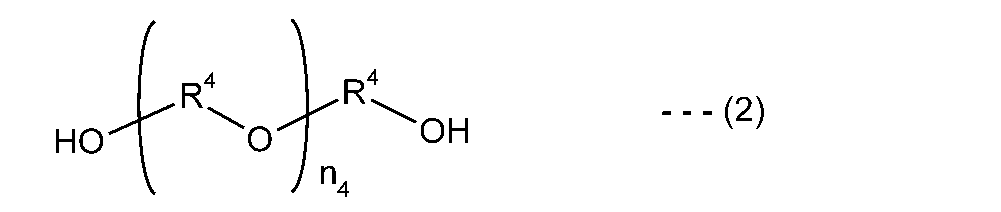
- the above-mentioned polyether polyol is obtained by dehydration condensation of a diol having 2 to 12 carbon atoms or ring-opening polymerization of an oxirane compound, oxetane compound or tetrahydrofuran compound having 2 to 12 carbon atoms. It is represented by the following structural formula (2).
- R 4 is a residue obtained by removing a hydroxyl group from the corresponding diol (HO—R 4 —OH) and is an alkylene group having 2 to 12 carbon atoms, and n 4 is a positive integer, preferably Is 4 to 50.
- the above diols having 2 to 12 carbon atoms may be used alone as a homopolymer or as a copolymer by using two or more kinds in combination.
- polyether polyol represented by the above formula (2) examples include polyethylene glycol, polypropylene glycol, poly-1,2-butylene glycol, polytetramethylene glycol (poly 1,4-butanediol), Examples thereof include polyalkylene glycols such as poly-3-methyltetramethylene glycol and polyneopentyl glycol. Further, for the purpose of improving the hydrophobicity of the polyether polyol, a copolymer of these, for example, a copolymer of 1,4-butanediol and neopentyl glycol can be used.
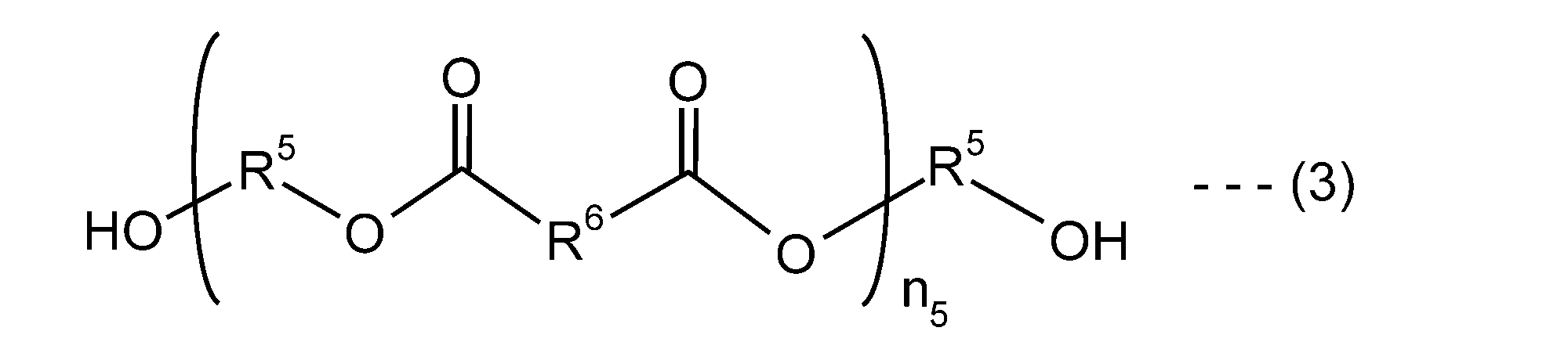
- the polyester polyol is obtained by dehydration condensation of dicarboxylic acid and diol or transesterification reaction of esterified product of lower alcohol of dicarboxylic acid and diol, and is represented by the following structural formula (3).
- R 5 is a residue obtained by removing a hydroxyl group from the corresponding diol (HO—R 5 —OH) and is an alkylene group having 2 to 10 carbon atoms or an organic group
- R 6 is a corresponding group.
- n 5 is a positive integer, preferably 2 to 50 Is.
- diol examples include ethylene glycol, 1,2-propanediol, 1,3-propanediol, 1,2-butanediol, 1,3-butanediol, and 1 ,4-butanediol, 1,5-pentanediol, 1,6-hexanediol, 3-methyl-1,5-pentanediol, 1,8-octanediol, 1,3-cyclohexanedimethanol, 1,4- Cyclohexanedimethanol, 1,9-nonanediol, 2-methyl-1,8-octanediol, 1,10-decamethylene glycol or 1,2-tetradecanediol, 2,4-diethyl-1,5-pentanediol, Butylethyl propane diol, 1,3-cyclohexane dimethanol, diethylene glycol, triethylene glycol
- dicarboxylic acid examples include succinic acid, glutaric acid, adipic acid, azelaic acid, sebacic acid, decanedicarboxylic acid, brassic acid, and 1,4-cyclohexanedicarboxylic acid.
- succinic acid glutaric acid, adipic acid, azelaic acid, sebacic acid, decanedicarboxylic acid, brassic acid, and 1,4-cyclohexanedicarboxylic acid.
- Hexahydrophthalic acid methyltetrahydrophthalic acid, endomethylenetetrahydrophthalic acid, methylendomethylenetetrahydrophthalic acid, chlorendic acid, fumaric acid, maleic acid, itaconic acid, citraconic acid.
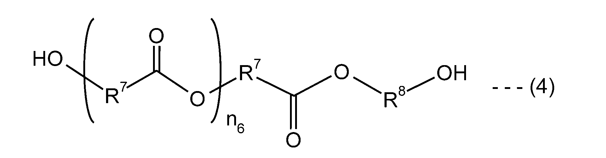
- the polylactone polyol is obtained by a condensation reaction between a ring-opening polymer of a lactone and a diol or a condensation reaction between a diol and a hydroxyalkanoic acid, and is represented by the following structural formula (4).
- R 7 is a residue obtained by removing a hydroxyl group and a carboxy group from the corresponding hydroxyalkanoic acid (HO—R 7 —COOH) and is an alkylene group having 4 to 8 carbon atoms
- R 8 is It is a residue obtained by removing a hydroxyl group from the corresponding diol (HO—R 8 —OH) and is an alkylene group having 2 to 10 carbon atoms
- n 6 is a positive integer, preferably 2 to 50.
- hydroxyalkanoic acid examples include 3-hydroxybutanoic acid, 4-hydroxypentanoic acid and 5-hydroxyhexanoic acid.
- lactone examples include ⁇ -caprolactone.
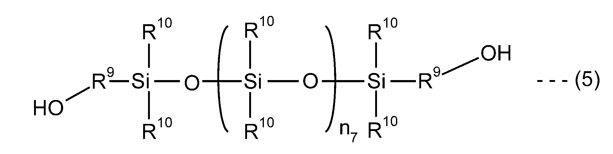
- both-end hydroxyl group-containing silicone is represented by, for example, the following structural formula (5).
- R 9 is independently an aliphatic hydrocarbon divalent residue having 2 to 50 carbon atoms
- n 7 is a positive integer, preferably 2 to 50.
- R 10's each independently represent an aliphatic hydrocarbon group having 1 to 12 carbon atoms.
- examples of commercially available products of the above-mentioned hydroxyl-terminated poly-silicone include "X-22-160AS, KF6001, KF6002, KF-6003" manufactured by Shin-Etsu Chemical Co., Ltd.
- polyol compound having 18 to 72 carbon atoms which is obtained by hydrogenating a polyvalent carboxylic acid derived from a C18 unsaturated fatty acid and a polymer thereof using a vegetable oil as a raw material and converting the carboxylic acid into a hydroxyl group
- polyol compound having 18 to 72 carbon atoms which is obtained by hydrogenating a polyvalent carboxylic acid derived from a C18 unsaturated fatty acid and a polymer thereof using a vegetable oil as a raw material and converting the carboxylic acid into a hydroxyl group
- diol compounds having a hydrogenated skeleton of dimer acid examples of commercially available products thereof include "Sovermol (registered trademark) 908" manufactured by Cognis.
- a diol having a molecular weight of 300 or less which is usually used as a diol component when synthesizing a polyester or a polycarbonate, can be used as the (a2) polyol compound.
- a low molecular weight diol include ethylene glycol, 1,2-propanediol, 1,3-propanediol, 1,2-butanediol, 1,3-butanediol and 1,4-butane.
- Diol 1,5-pentanediol, 1,6-hexanediol, 3-methyl-1,5-pentanediol, 1,8-octanediol, 1,3-cyclohexanedimethanol, 1,4-cyclohexanedimethanol, 1,9-nonanediol, 2-methyl-1,8-octanediol, 1,10-decamethylene glycol, 1,2-tetradecanediol, 2,4-diethyl-1,5-pentanediol, butylethylpropanediol , 1,3-cyclohexanedimethanol, diethylene glycol, triethylene glycol, dipropylene glycol and the like.
- (A3) Carboxyl group-containing dihydroxy compound (a3) The carboxy group-containing dihydroxy compound has a molecular weight of 200 or less having two selected from a hydroxy group and a hydroxyalkyl group having 1 or 2 carbon atoms.
- the carboxylic acid or aminocarboxylic acid is preferable because the crosslinking point can be controlled. Specific examples include 2,2-dimethylolpropionic acid, 2,2-dimethylolbutanoic acid, N,N-bishydroxyethylglycine, N,N-bishydroxyethylalanine, etc. From the solubility of 2,2-dimethylolpropionic acid and 2,2-dimethylolbutanoic acid are particularly preferable.
- These (a3) carboxy group-containing dihydroxy compounds can be used alone or in combination of two or more.
- the aforementioned (A) carboxy group-containing polyurethane can be synthesized from only the above-mentioned three components ((a1), (a2) and (a3)). In addition, it can also be synthesized by further reacting the (a4) monohydroxy compound and/or the (a5) monoisocyanate compound. From the viewpoint of light resistance, it is preferable to use a compound containing no aromatic ring or carbon-carbon double bond in the molecule.
- (A4) Monohydroxy compound examples include compounds having a carboxylic acid such as glycolic acid and hydroxypivalic acid.
- the (a4) monohydroxy compound may be used alone or in combination of two or more kinds.
- (a4) monohydroxy compounds include methanol, ethanol, n-propanol, isopropanol, n-butanol, isobutanol, sec-butanol, t-butanol, amyl alcohol, hexyl alcohol, octyl alcohol and the like.
- (A5) Monoisocyanate compound examples include hexyl isocyanate and dodecyl isocyanate.
- the above-mentioned (A) carboxy group-containing polyurethane is a polyisocyanate compound (a1) as described above, (a1) using a suitable organic solvent in the presence or absence of a known urethanization catalyst such as dibutyltin dilaurylate. Synthesis can be performed by reacting a2) a polyol compound and (a3) a carboxy group-containing dihydroxy compound, but it is preferable to react without a catalyst because it is not necessary to consider tin and the like in the end.
- the organic solvent is not particularly limited as long as it has low reactivity with an isocyanate compound, but does not contain a basic functional group such as amine, and has a boiling point of 50°C or higher, preferably 80°C or higher, more preferably 100°C or higher. Certain solvents are preferred.
- Examples of such a solvent include toluene, xylene, ethylbenzene, nitrobenzene, cyclohexane, isophorone, diethylene glycol dimethyl ether, ethylene glycol diethyl ether, ethylene glycol monomethyl ether acetate, propylene glycol monomethyl ether acetate, Propylene glycol monoethyl ether acetate, dipropylene glycol monomethyl ether acetate, diethylene glycol monoethyl ether acetate, methyl methoxypropionate, ethyl methoxypropionate, methyl ethoxypropionate, ethyl ethoxypropionate, ethyl acetate, acetic acid Examples thereof include n-butyl, isoamyl acetate, ethyl lactate, acetone, methyl ethyl ketone, cyclohexanone, N,N-dimethylformamide, N
- an organic solvent having a low solubility of the generated polyurethane is not preferable and that polyurethane is used as a raw material of the ink for a protective film in electronic material applications, among these, particularly, propylene glycol monomethyl ether acetate.
- Preferred are propylene glycol monoethyl ether acetate, dipropylene glycol monomethyl ether acetate, diethylene glycol monoethyl ether acetate and ⁇ -butyrolactone.
- the raw materials are charged, but usually (a2) the polyol compound and (a3) the dihydroxy compound having a carboxy group are charged in advance and dissolved or dispersed in a solvent, and then 20 to 150° C. More preferably, the polyisocyanate compound (a1) is added dropwise at 60 to 120° C., and then they are reacted at 30 to 160° C., more preferably 50 to 130° C.
- the charged molar ratio of the raw materials is adjusted according to the molecular weight and acid value of the desired polyurethane.
- the terminal of the polyurethane molecule should be an isocyanato group, It is necessary to use the polyisocyanate compound (a1) in excess of the polyol compound (a2) and the dihydroxy compound having a carboxyl group (a3) (so that the isocyanato groups are in excess of the total of the hydroxyl groups).
- the (a5) monoisocyanate compound is introduced into the polyurethane, the (a1) polyisocyanate compound rather than the (a2) polyol compound and the (a3) carboxy-containing dihydroxy compound so that the terminal of the polyurethane molecule becomes a hydroxy group. Should be used in a smaller amount (so that there are less isocyanato groups than the total of hydroxyl groups).
- these charging molar ratios are such that (a1) isocyanato group of polyisocyanate compound: ((a2) hydroxyl group of polyol compound+(a3) hydroxyl group of dihydroxy compound having carboxy group) is 0.5 to 1 0.5:1, preferably 0.8 to 1.2:1, more preferably 0.95 to 1.05:1.
- the hydroxyl group of the (a2) polyol compound is 1:0.1 to 30, preferably 1:0.3 to 10.
- the number of moles of the (a1) polyisocyanate compound is made larger than the number of moles of ((a2) polyol compound + (a3) dihydroxy compound having a carboxy group), and (a4) It is preferable to use the monohydroxy compound in a molar amount of 0.5 to 1.5 times, preferably 0.8 to 1.2 times the molar amount of the excess isocyanato group.
- the number of moles of ((a2) polyol compound+(a3) dihydroxy compound having a carboxy group) is set to be larger than the number of moles of (a1) polyisocyanate compound, and an excess of hydroxyl groups is obtained. It is preferably used in an amount of 0.5 to 1.5 times, and preferably 0.8 to 1.2 times the molar amount.
- the reaction between the (a2) polyol compound and the (a3) carboxy group-containing dihydroxy compound and the (a1) polyisocyanate compound is almost the same.
- the (a4) monohydroxy compound was added to the reaction solution in an amount of 20%. Dropwise at ⁇ 150° C., more preferably 70 ⁇ 120° C., then hold at the same temperature to complete the reaction.
- Examples of the (B) epoxy compound include bisphenol A type epoxy compound, hydrogenated bisphenol A type epoxy resin, bisphenol F type epoxy resin, novolac type epoxy resin, phenol novolac type epoxy resin, cresol novolac type epoxy resin, N-glycidyl type.
- Epoxy resin bisphenol A novolac type epoxy resin, chelate type epoxy resin, glyoxal type epoxy resin, amino group containing epoxy resin, rubber modified epoxy resin, dicyclopentadiene phenolic type epoxy resin, silicone modified epoxy resin, ⁇ -caprolactone modified epoxy resin
- An epoxy compound having two or more epoxy groups in one molecule such as a resin, an aliphatic epoxy resin containing a glycidyl group, and an alicyclic epoxy resin containing a glycidyl group can be mentioned.
- an epoxy compound having three or more epoxy groups in one molecule can be more preferably used.
- examples of such epoxy compounds include EHPE (registered trademark) 3150 (manufactured by Daicel Chemical Co., Ltd.), jER604 (manufactured by Mitsubishi Chemical Co., Ltd.), EPICLON EXA-4700 (manufactured by DIC Corporation), EPICLON HP-7200 (manufactured by DIC Corporation) , Pentaerythritol tetraglycidyl ether, pentaerythritol triglycidyl ether, TEPIC-S (manufactured by Nissan Chemical Co., Ltd.) and the like.
- the (B) epoxy compound may have an aromatic ring in the molecule, in which case the mass of (B) is 20 mass% or less with respect to the total mass of (A) and (B). preferable.
- the compounding ratio of the (A) carboxy group-containing polyurethane to the (B) epoxy compound is 0.5 to 1.5 in terms of the equivalent ratio of the carboxy group in the polyurethane to the epoxy group of the (B) epoxy compound. It is preferably 0.7 to 1.3, more preferably 0.9 to 1.1.
- curing accelerator (C) examples include phosphine compounds such as triphenylphosphine and tributylphosphine (manufactured by Kitako Chemical Co., Ltd.), Cureazole (registered trademark) (imidazole epoxy resin curing agent: manufactured by Shikoku Kasei Co., Ltd.), and 2-phenyl. -4-Methyl-5-hydroxymethylimidazole, U-CAT (registered trademark) SA series (DBU salt: manufactured by San-Apro), Irgacure (registered trademark) 184 and the like can be mentioned.
- phosphine compounds such as triphenylphosphine and tributylphosphine (manufactured by Kitako Chemical Co., Ltd.)
- Cureazole registered trademark
- imidazole epoxy resin curing agent manufactured by Shikoku Kasei Co., Ltd.
- 2-phenyl. -4-Methyl-5-hydroxymethylimidazole U-CAT
- the amount added is 0.1 to 10% with respect to the total mass of (A) and (B). 10% by mass, more preferably 0.5 to 6% by mass, even more preferably 0.5 to 5% by mass, particularly preferably 0.5 to 3% by mass.
- a curing aid may be used in combination.
- the curing aid include polyfunctional thiol compounds and oxetane compounds.
- polyfunctional thiol compounds are pentaerythritol tetrakis(3-mercaptopropionate), tris-[(3-mercaptopropionyloxy)-ethyl]-isocyanurate, trimethylolpropane tris(3-mercaptopropionate), Karens (Registered trademark) MT series (manufactured by Showa Denko KK) and the like.
- oxetane compound examples include Aron oxetane (registered trademark) series (manufactured by Toagosei Co., Ltd.), ETERNACOLL (registered trademark) OXBP, and OXMA (manufactured by Ube Industries).
- Aron oxetane registered trademark
- ETERNACOLL registered trademark
- OXBP registered trademark
- OXMA manufactured by Ube Industries
- the curable resin composition preferably contains the solvent (D) in an amount of 95.0% by mass or more and 99.9% by mass or less, more preferably 96% by mass or more and 99.7% by mass or less, and 97% by mass or more. It is more preferable that the content is 99.5% by mass or less.
- the solvent (D) the solvent used for synthesizing the polyurethane containing the carboxyl group (A) may be used as it is, or another solvent may be used for adjusting the solubility and printability of the polyurethane resin. Can also When another solvent is used, the reaction solvent may be distilled off before and after adding a new solvent to replace the solvent.
- the boiling point of the solvent is preferably 80°C to 300°C, more preferably 80°C to 250°C.
- the boiling point is less than 80°C, it is easy to dry during printing and unevenness is likely to occur.
- the boiling point is higher than 300°C, heat treatment at a high temperature for a long time is required at the time of drying and curing, which is not suitable for industrial production.
- solvent (D) examples include propylene glycol monomethyl ether acetate (boiling point 146° C.), ⁇ -butyrolactone (boiling point 204° C.), diethylene glycol monoethyl ether acetate (boiling point 218° C.), tripropylene glycol dimethyl ether (boiling point 243).
- solvents may be used alone or in combination of two or more.
- the solubility of the polyurethane resin, epoxy resin, etc. to be used is taken into consideration to cause aggregation or precipitation. It is preferable to use a solvent having a hydroxyl group having a boiling point of more than 100° C. or a solvent having a boiling point of 100° C. or less from the viewpoint of ink drying property.
- the curable resin composition comprises the above (A) carboxy group-containing polyurethane, (B) epoxy compound, (C) curing accelerator, (D) solvent, and (D) solvent content. It can be produced by mixing 95.0% by mass or more and 99.9% by mass or less and stirring the mixture so as to be uniform.
- the solid content concentration in such a curable resin composition varies depending on the desired film thickness and printing method, but is preferably 0.1 to 10% by mass, and 0.5 to 5% by mass. Is more preferable.
- the solid content concentration is in the range of 0.1 to 10% by mass, the problem that electrical contact cannot be made due to the film thickness becoming too thick when applied on the transparent conductive film, and sufficient A protective film having weather resistance and light resistance can be obtained.
- a protective film ((A) a carboxyl group-containing polyurethane which is a solid content in the curable resin composition, (B) an epoxy compound, and (C) a curing residue in a curing accelerator)
- the ratio of the aromatic ring-containing compound defined by the following formula contained therein is preferably suppressed to 15% by mass or less.
- the term "(C) curing residue in the curing accelerator” as used herein means that some or all of the (C) curing accelerator disappears (decomposes, volatilizes, etc.) depending on the curing conditions, so it is protected under the curing conditions. It means (C) a curing accelerator remaining in the film.
- the "aromatic ring-containing compound” means a compound having at least one aromatic ring in the molecule.
- Ratio of aromatic ring-containing compound [(amount of aromatic ring-containing compound used)/(mass of protective film (mass of polyurethane containing (A) carboxy group + mass of (B) epoxy compound + (C) curing residue in curing accelerator) Group)] ⁇ 100 (%)
- a curable resin composition on a substrate having a metal nanowire layer formed by a printing method such as a bar coating printing method, a gravure printing method, an inkjet method, or a slit coating method.
- a printing method such as a bar coating printing method, a gravure printing method, an inkjet method, or a slit coating method.
- the solvent is dried and removed, and then the curable resin is cured to form a protective film.
- the thickness of the protective film obtained after curing is more than 100 nm and 1 ⁇ m or less.
- the thickness of the protective film is preferably more than 100 nm and not more than 500 nm, more preferably more than 100 nm and not more than 200 nm, further preferably more than 100 nm and not more than 150 nm, particularly preferably more than 100 nm and not more than 120 nm. If the thickness exceeds 1 ⁇ m, it becomes difficult to establish electrical continuity with the wiring in the subsequent process.
- the transparent conductive substrate obtained by sequentially forming the transparent conductive film (silver nanowire layer) and the protective film on the transparent substrate has excellent bending resistance.
- the bending test with respect to the resistance value (R 0 ) of the transparent conductive substrate before being subjected to the bending test of bending the transparent conductive substrate 200,000 times
- the ratio (R/R 0 ) of the resistance value (R) after being subjected to the heat treatment is preferably 2.0 or less, more preferably 1.5 or less, and further preferably 1.2 or less. preferable.
- the obtained silver nanowire coarse dispersion is dispersed in 2000 ml of methanol, and a tabletop small tester (manufactured by NGK Insulators Co., Ltd., using a ceramic membrane filter sepilt, membrane area 0.24 m 2 , pore diameter 2.0 ⁇ m, size ⁇ 30 mm ⁇ 250 mm, filtration)
- the mixture was poured into a differential pressure of 0.01 MPa) and subjected to cross-flow filtration at a circulation flow rate of 12 L/min and a dispersion liquid temperature of 25° C. to remove impurities to obtain silver nanowires (average diameter: 26 nm, average length: 20 ⁇ m). ..
- a field emission scanning electron microscope JSM-7000F (made by JEOL Ltd.) was used to measure the diameters of 100 arbitrarily selected silver nanowires, and the arithmetic mean thereof was calculated. It was calculated as a value.
- the shape measurement laser microscope VK-X200 (manufactured by KEYENCE CORPORATION) was used to calculate the average length of the obtained silver nanowires, and the length of 100 silver nanowires arbitrarily selected was measured and the arithmetic operation was performed. It was calculated as an average value.
- methanol, ethylene glycol, AgNO 3 , and FeCl 3 reagents manufactured by Fuji Film Wako Pure Chemical Industries, Ltd. were used.
- the thermal decomposition starting temperature of PNVA (registered trademark) was measured using TG-DTA2000 manufactured by NETZSCH. Put about 10mg of sample into a platinum pan and measure it in air atmosphere as follows. Temperature above 120°C (Because the sample is not pre-dried, weight loss due to moisture absorbed by the sample near 100°C is reduced. Was observed, and the effect of ignoring the influence was noted), and the temperature at which a weight loss of 1% occurred was determined as the thermal decomposition start temperature. Air atmosphere, temperature conditions: room temperature ⁇ (10°C/min) ⁇ 700°C (compressor air 100 mL/min)
- the thermal decomposition starting temperature of PNVA (registered trademark) used in the preparation of the silver nanowire ink was 270°C.
- Table 1 shows the concentration of silver nanowires contained in the obtained silver nanowire ink.
- the obtained silver concentration was measured with a Varian AA280Z Zeeman atomic absorption spectrophotometer.
- a plasma treatment device AP-T03 manufactured by Sekisui Chemical Co., Ltd.
- ZF14-013 manufactured by Zeon Corporation, glass transition temperature 136° C. [catalog value], thickness 13 ⁇ m
- TQC automatic film applicator standard manufactured by Cotec Corp.
- wireless bar coater OSP-CN wireless bar coater
- the film thickness of the silver nanowire layer was measured using a film thickness measurement system F20-UV (manufactured by Filmetrics Co., Ltd.) based on the optical interference method. The measurement point was changed and the average value of three points was used as the film thickness. A spectrum from 450 nm to 800 nm was used for the analysis. According to this measuring system, the film thickness (T c ) of the silver nanowire layer formed on the transparent substrate can be directly measured. The measurement results are shown in Table 1.
- the temperature of the reaction solution was lowered to 70° C., and Desmodur (registered trademark)-W (bis-(4-isocyanatocyclohexyl)methane) as polyisocyanate, manufactured by Sumika Covestro Urethane Co., Ltd., was added with a dropping funnel to give 59.69 g. Was added dropwise over 30 minutes.
- the temperature was raised to 120° C. and the reaction was carried out at 120° C. for 6 hours.
- 0.5 g of isobutanol was added, and the reaction was further conducted at 120° C. for 6 hours. went.
- the weight average molecular weight of the obtained carboxy group-containing polyurethane determined by GPC was 32300, and the acid value of the resin solution was 35.8 mgKOH/g.
- Comparative Synthesis Example 1 Synthesis of Original Resin Used in Curable Resin Composition PH-50
- the polyol compound in Working Synthesis Example 1 was converted into PH-50 (produced by Ube Industries, Ltd., polycarbonate diol, average molecular weight of about 500) from 42.32 g of C-1015N. )
- a carboxy group-containing polyurethane was obtained by performing the same operation except that the amount of Desmodur (registered trademark)-W 59.69 g was changed to 66.64 g instead of 35.37 g.
- the weight average molecular weight was 33100, and the acid value of the resin solution was 35.3 mgKOH/g.
- Implementation curable resin composition 1 (OC022) 10.0 g of a solution of the polyurethane containing carboxy group (A) (carboxyl group-containing polyurethane content: 45% by mass) obtained in the above Synthesis Example 1 was weighed into a poly container and 1-hexanol was used as the solvent (D). 85.3 g and ethyl acetate 85.2 g were added, and the mixture was stirred with Mix Rotor VMR-5R (manufactured by As One Co., Ltd.) for 12 hours at room temperature in the atmosphere (rotation speed 100 rpm).
- Mix Rotor VMR-5R manufactured by As One Co., Ltd.
- Comparative curable resin composition 1 (PH-50) 10.0 g of the (A) carboxy group-containing polyurethane solution (carboxyl group-containing polyurethane content: 45% by mass) obtained in Comparative Synthesis Example 1 above was weighed into a poly container, and (D) 1-hexanol was used as a solvent. 85.0 g and ethyl acetate 85.0 g were added, and the mixture was stirred with a mix rotor VMR-5R (manufactured by As One Co., Ltd.) for 12 hours at room temperature in the atmosphere (rotation speed 100 rpm).
- VMR-5R manufactured by As One Co., Ltd.
- Comparative Examples 1 and 2 were coated using a wireless bar coater OSP-CN-05M so that the wet film thickness was 5 ⁇ m. These wet film thicknesses are adjusted so that the thickness of the protective film after drying has a desired value. Then, hot air drying (thermosetting) was performed for 1 minute at 80° C. in a thermostat HISPEC HS350 (manufactured by Kusumoto Kasei Co., Ltd.) in an air atmosphere to form a protective film to prepare a transparent conductive substrate.
- a wireless bar coater OSP-CN-05M so that the wet film thickness was 5 ⁇ m. These wet film thicknesses are adjusted so that the thickness of the protective film after drying has a desired value. Then, hot air drying (thermosetting) was performed for 1 minute at 80° C. in a thermostat HISPEC HS350 (manufactured by Kusumoto Kasei Co., Ltd.) in an air atmosphere to form a protective film to prepare a transparent conductive substrate.
- the film thickness of the protective film was measured using the film thickness measurement system F20-UV (manufactured by Filmetrics Co., Ltd.) based on the optical interference method like the film thickness of the silver nanowire layer described above. The measurement point was changed and the average value of three points was used as the film thickness. A spectrum from 450 nm to 800 nm was used for the analysis.
- the total film thickness of the film thickness of the silver nanowire layer formed on the transparent substrate (T c) and the thickness of the protective film formed thereon (T p) (T c + T p ) can be directly measured, the film thickness (T p ) of the protective film can be obtained by subtracting the film thickness (T c ) of the silver nanowire layer previously measured from this measured value.
- Table 1 The measurement results are summarized in Table 1.
- a clamshell-type endurance tester (Small tabletop endurance test system Tension-Free (registered trademark) Folding Clamshell-type (manufactured by Yuasa System Instruments Co., Ltd.)) capable of 180° bending test was used.
- a test piece was prepared by cutting a size of 15 mm ⁇ 150 mm from the A4 size transparent conductive substrate and forming a terminal portion with silver paste so that the distance between terminals was 80 mm.
- a conductive paste DW-420L-2A (manufactured by Toyobo Co., Ltd.) was applied by hand coating in an area of about 2 mm square, and then a thermostat HISPEC HS350 (manufactured by Kusumoto Kasei) was used at 80° C. for 30 minutes in the atmosphere.
- the terminal portion was formed by drying with hot air in an atmosphere.
- the produced test piece was fixed with a tape so that the center of the distance between the terminals and the center of the bent portion of the device were aligned.
- the change in resistance between terminals was evaluated.
- the resistance value between the silver paste terminals formed by the above-described method was measured by using a digital multimeter PC5000a (manufactured by Sanwa Electric Keiki Co., Ltd.), and the resistance value (R 0 ) before the bending test and the bending test (20
- the change in resistance was evaluated by measuring the resistance value (R) after each folding and folding operation repeatedly and calculating the ratio (R/R 0 ) of the resistance value after the bending test before the start of the bending test.
- Examples 1 and 3 and Comparative Examples 1 and 2 were attached so that the coated surface faces upward (valley fold), and Example 2 is attached such that the coated surface faces downward (mountain fold).
- Table 1 The evaluation results are summarized in Table 1.
- a transparent conductive film having excellent flexibility can be realized, which is suitable for a bendable touch panel application.
- FIG. 1(a), (b), (a) shows a configuration of a typical out-cell (a system in which a touch panel is attached to a display) capacitive touch panel in which the transparent conductive substrate of the present invention is considered. It is shown in c).
- 1A and 1B show a capacitive touch panel having a structure in which two layers of sensor electrodes are formed on a film substrate (COP) which is a transparent substrate
- FIG. 1C shows a film substrate ( It is a capacitive touch panel having a structure in which two films each having one sensor electrode formed on a COP) are laminated.
- 1A, 1 ⁇ /b>B, and 1 ⁇ /b>C is an active matrix drive type organic EL (Active Matrics Organic Light Emitting Diode) to which the capacitive touch panel according to this embodiment is attached. ) Represents a display.
- organic EL Active Matrics Organic Light Emitting Diode
- the capacitive touch panel 10 is attached on the AMOLED 100 via the thin film sealing 102.
- the capacitive touch panel 10 is attached to the thin film encapsulation 102 with an adhesive sheet (optical glue) 12.
- an adhesive sheet optical glue
- a protective film 14 On the adhesive sheet 12, a protective film 14, a transparent conductive film (silver nanowire layer) 16y, a cycloolefin polymer (COP) film 18, a transparent conductive film 16x, a protective film 14, a circularly polarizing plate 20, an adhesive sheet 12, a cover film.
- COP cycloolefin polymer
- the transparent conductive film 16x constitutes a sensor electrode in the x direction and the transparent conductive film 16y constitutes a sensor electrode in the y direction.
- the cycloolefin polymer (COP) film 18, the transparent conductive film 16xy, the protective film 14 are provided on the adhesive sheet 12 to which the thin film encapsulation 102 and the capacitive touch panel 10 are attached.
- the insulating film 24, the bridge electrode 26, the circularly polarizing plate 20, the adhesive sheet 12, and the cover film 22 are laminated in this order to form the bridge electrode type capacitive touch panel 10.
- the transparent conductive film 16xy is a transparent conductive film having sensor electrodes in the x direction and the y direction formed on the same surface.
- the cycloolefin polymer (COP) film 18, the transparent conductive film 16 y, the protective film 14 are provided on the adhesive sheet 12 to which the thin film encapsulation 102 and the capacitive touch panel 10 are attached.
- the adhesive sheet 12, the cycloolefin polymer (COP) film 18, the transparent conductive film 16x, the protective film 14, the circularly polarizing plate 20, the adhesive sheet 12, and the cover film 22 are laminated in this order to form the capacitive touch panel 10. I am configuring.
- FIG. 1C the cycloolefin polymer (COP) film 18, the transparent conductive film 16 y, the protective film 14 are provided on the adhesive sheet 12 to which the thin film encapsulation 102 and the capacitive touch panel 10 are attached.
- the adhesive sheet 12, the cycloolefin polymer (COP) film 18, the transparent conductive film 16x, the protective film 14, the circularly polarizing plate 20, the adhesive sheet 12, and the cover film 22 are laminated in this order to form the capacitive touch panel
- the cycloolefin polymer (COP) film 18, the transparent conductive film 16y, and the protective film 14 are laminated in this order on the transparent conductive film 16y and the cycloolefin polymer (COP) film.
- the transparent conductive film 16x, and the protective film 14 are laminated in this order to the cycloolefin polymer (COP) film 18 of the laminate, and the adhesive sheet 12 is interposed between the film substrate (the cycloolefin polymer (COP) film
- the combination of the cycloolefin polymer (COP) film 18, the transparent conductive films 16x, 16y or 16xy, and the protective film 14 provides the transparent conductive substrate according to the embodiment. They are formed, and can be manufactured by the method of forming the silver nanowire layer and the protective film of the above-described examples.
Landscapes
- Engineering & Computer Science (AREA)
- Chemical & Material Sciences (AREA)
- General Engineering & Computer Science (AREA)
- Theoretical Computer Science (AREA)
- Polymers & Plastics (AREA)
- Organic Chemistry (AREA)
- Physics & Mathematics (AREA)
- Health & Medical Sciences (AREA)
- Chemical Kinetics & Catalysis (AREA)
- Medicinal Chemistry (AREA)
- General Physics & Mathematics (AREA)
- Human Computer Interaction (AREA)
- Dispersion Chemistry (AREA)
- Spectroscopy & Molecular Physics (AREA)
- Laminated Bodies (AREA)
- Non-Insulated Conductors (AREA)
Abstract
Description
上記透明基材は着色していてもよいが、全光線透過率(可視光に対する透明性)は高い方が好ましく、全光線透過率が80%以上であることが好ましい。例えば、ポリエステル(ポリエチレンテレフタレート[PET]、ポリエチレンナフタレート[PEN]等)、ポリカーボネート、アクリル樹脂(ポリメチルメタクリレート[PMMA]等)、シクロオレフィンポリマー等の樹脂フィルムを好適に使用することができる。また、これら透明基材には光学特性、電気的特性や耐屈曲性を損なわない範囲で、易接着、光学調整(アンチグレア、アンチリフレクションなど)、ハードコートなどの機能を有する層を、単一または複数備えていてもよく、片面または両面に備えていてもよい。これらの樹脂フィルムの中でも、優れた光透過性(透明性)や柔軟性、機械的特性などの点からポリエチレンテレフタレート、シクロオレフィンポリマーを用いることが好ましい。シクロオレフィンポリマーとしては、ノルボルネンの水素化開環メタセシス重合型シクロオレフィンポリマー(ZEONOR(登録商標、日本ゼオン社製)、ZEONEX(登録商標、日本ゼオン社製)、ARTON(登録商標、JSR社製)等)やノルボルネン/エチレン付加共重合型シクロオレフィンポリマー(APEL(登録商標、三井化学社製)、TOPAS(登録商標、ポリプラスチックス社製))を用いることができる。これらの中でもガラス転移温度(Tg)が90~170℃のものが引き出し配線やコネクタ部分などの後工程における加熱に耐えうるため好ましく、125~145℃のものがより好ましい。厚みは1~20μmであることが好ましく、5~20μmであることがより好ましく、8~20μmがさらに好ましい。
透明導電膜を構成する上記導電性繊維としては、金属ナノワイヤ、カーボン繊維などが挙げられ、金属ナノワイヤを好適に使用することができる。金属ナノワイヤは、径がナノメーターオーダーのサイズである金属であり、ワイヤ状の形状を有する導電性材料である。なお、本実施形態では、金属ナノワイヤとともに(混合して)、または金属ナノワイヤに代えて、ポーラスあるいはノンポーラスのチューブ状の形状を有する導電性材料である金属ナノチューブを使用してもよい。本明細書において、「ワイヤ状」と「チューブ状」はいずれも線状であるが、前者は中央が中空ではないもの、後者は中央が中空であるものを意図する。性状は、柔軟であってもよく、剛直であってもよい。前者を「狭義の金属ナノワイヤ」、後者を「狭義の金属ナノチューブ」と呼び、以下、本願明細書において、「金属ナノワイヤ」は狭義の金属ナノワイヤと狭義の金属ナノチューブとを包括する意味で用いる。狭義の金属ナノワイヤ、狭義の金属ナノチューブは、単独で用いてもよく、混合して用いてもよい。
下記溶離液にバインダー樹脂を溶解させ、20時間静置した。この溶液におけるバインダー樹脂の濃度は0.05質量%である。
GPC:昭和電工株式会社製Shodex(登録商標)SYSTEM21
カラム:東ソー株式会社製TSKgel(登録商標)G6000PW
カラム温度:40℃
溶離液:0.1mol/L NaH2PO4水溶液+0.1mol/L Na2HPO4水溶液
流速 :0.64mL/min
試料注入量:100μL
MALS検出器:ワイアットテクノロジーコーポレーション、DAWN(登録商標) DSP
レーザー波長:633nm
多角度フィット法:Berry法
透明導電膜を保護する保護膜は、硬化性樹脂組成物の硬化膜である。硬化性樹脂組成物としては、(A)カルボキシ基を含有するポリウレタンと、(B)エポキシ化合物と、(C)硬化促進剤と、(D)溶媒と、を含むものが好ましい。硬化性樹脂組成物を上記透明導電膜上に印刷、塗布等により形成し、硬化させて保護膜を形成する。硬化性樹脂組成物の硬化は、例えば熱硬化性樹脂組成物を用いる場合、これを加熱・乾燥させることにより行うことができる。
装置名:日本分光株式会社製HPLCユニット HSS-2000
カラム:ShodexカラムLF-804
移動相:テトラヒドロフラン
流速 :1.0mL/min
検出器:日本分光株式会社製 RI-2031Plus
温度 :40.0℃
試料量:サンプルル-プ 100μリットル
試料濃度:約0.1質量%に調製
酸価(mg-KOH/g)=〔B×f×5.611〕/S
B:0.1N水酸化カリウム-エタノール溶液の使用量(ml)
f:0.1N水酸化カリウム-エタノール溶液のファクター
S:試料の採取量(g)
(a1)ポリイソシアネート化合物としては、通常、1分子当たりのイソシアナト基が2個であるジイソシアネートが用いられる。ポリイソシアネート化合物としては、たとえば、脂肪族ポリイソシアネート、脂環式ポリイソシアネート等が挙げられ、これらの1種を単独でまたは2種以上を組み合わせて用いることができる。(A)カルボキシ基を含有するポリウレタンがゲル化をしない範囲で、イソシアナト基を3個以上有するポリイソシアネートも少量使用することができる。
(a2)ポリオール化合物(ただし、(a2)ポリオール化合物には、後述する(a3)カルボキシ基を有するジヒドロキシ化合物は含まれない。)の数平均分子量は通常250~50,000であり、好ましくは400~10,000、より好ましくは500~5,000である。この分子量は前述した条件でGPCにより測定したポリスチレン換算の値である。

(a3)カルボキシ基を含有するジヒドロキシ化合物としては、ヒドロキシ基、炭素数が1または2のヒドロキシアルキル基から選択されるいずれかを2つ有する分子量が200以下のカルボン酸またはアミノカルボン酸であることが架橋点を制御できる点で好ましい。具体的には2,2-ジメチロ-ルプロピオン酸、2,2-ジメチロ-ルブタン酸、N,N-ビスヒドロキシエチルグリシン、N,N-ビスヒドロキシエチルアラニン等が挙げられ、この中でも、溶媒への溶解度から、2,2-ジメチロ-ルプロピオン酸、2,2-ジメチロ-ルブタン酸が特に好ましい。これらの(a3)カルボキシ基を含有するジヒドロキシ化合物は、1種単独でまたは2種以上を組み合わせて用いることができる。
(a4)モノヒドロキシ化合物として、グリコール酸、ヒドロキシピバリン酸等カルボン酸を有する化合物が挙げられる。
(a5)モノイソシアネート化合物としては、ヘキシルイソシアネート、ドデシルイソシアネート等が挙げられる。
銀ナノワイヤインクを作製したのち、透明基材の一方の主面上に塗布、乾燥して銀ナノワイヤ層を形成した。続いて硬化性樹脂組成物を作製したのち、前記銀ナノワイヤ層の上に塗布、乾燥して保護膜を形成し、透明導電基体を作製した。この透明導電基体に対し、屈曲試験をはじめとする各種性能評価試験を行った。
ポリビニルピロリドンK-90((株)日本触媒社製)(0.98g)、AgNO3(1.04g)及びFeCl3(0.8mg)を、エチレングリコール(250ml)に溶解し、150℃で1時間加熱反応した。得られた銀ナノワイヤ粗分散液をメタノール2000mlに分散させ、卓上小型試験機(日本ガイシ株式会社製、セラミック膜フィルター セフィルト使用、膜面積0.24m2、孔径2.0μm、寸法Φ30mm×250mm、ろ過差圧0.01MPa)に流し入れ、循環流速12L/min、分散液温度25℃にてクロスフロー濾過を実施し不純物を除去し、銀ナノワイヤ(平均直径:26nm、平均長さ:20μm)を得た。得られた銀ナノワイヤの平均径の算出には、電界放出形走査電子顕微鏡JSM-7000F(日本電子株式会社製)を用い、任意に選択した100本の銀ナノワイヤの直径を測定し、その算術平均値として求めた。また、得られた銀ナノワイヤの平均長の算出には、形状測定レーザマイクロスコープVK-X200(キーエンス株式会社製)を用い、任意に選択した100本の銀ナノワイヤの長さを測定し、その算術平均値として求めた。また、上記メタノール、エチレングリコール、AgNO3、FeCl3は富士フィルム和光純薬株式会社製試薬を用いた。
上記ポリオール法で合成した銀ナノワイヤの水/メタノール/エタノール混合溶媒の分散液11g(銀ナノワイヤ濃度0.62質量%、水/メタノール/エタノール=10:20:70[質量比])、水2.4g、メタノール3.6g(富士フィルム和光純薬株式会社製)、エタノール8.3g(富士フィルム和光純薬株式会社製)、プロピレングリコールモノメチルエーテル(PGME、富士フィルム和光純薬株式会社製)12.8g、プロピレングリコール1.2g(PG、AGC株式会社製)、PNVA(登録商標)水溶液(昭和電工株式会社製、固形分濃度10質量%、重量平均分子量90万)0.7gを混合し、ミックスローターVMR-5R(アズワン株式会社製)で1時間、室温、大気雰囲気下で撹拌(回転速度100rpm)して銀ナノワイヤインク40gを作製した。
空気雰囲気、温度条件:室温→(10℃/min)→700℃(コンプレッサーエアー100mL/min)
プラズマ処理装置(積水化学工業株式会社製AP-T03)を用いてプラズマ処理(使用ガス:窒素、搬送速度:50mm/sec、処理時間:6sec、設定電圧:400V)した、透明基材としてのA4サイズのシクロオレフィンポリマーフィルムZF14-013(日本ゼオン株式会社製、ガラス転移温度136℃[カタログ値]、厚み13μm)上に、TQC自動フィルムアプリケータースタンダード(コーテック株式会社製)とワイヤレスバーコータOSP-CN-22L(コーテック株式会社製)とを用い、ウェット膜厚が22μmとなるように銀ナノワイヤインクを透明基材(ZF14-013)の全面に塗布した(塗工速度100mm/sec)。その後、恒温器HISPEC HS350(楠本化成製)で80℃、1分間、大気雰囲気下で熱風乾燥し、銀ナノワイヤ層を形成した。
銀ナノワイヤ層の膜厚は光干渉法に基づく膜厚測定システムF20-UV(フィルメトリクス株式会社製)を用いて測定した。測定箇所を変え、3点測定した平均値を膜厚として用いた。解析には450nmから800nmのスペクトルを用いた。この測定システムによると、透明基材上に形成された銀ナノワイヤ層の膜厚(Tc)が直接測定できる。測定結果を表1に示す。
(A)カルボキシ基を含有するポリウレタンの合成例
実施合成例1 硬化性樹脂組成物OC022に用いる元樹脂の合成
攪拌装置、温度計、コンデンサーを備えた2L三口フラスコに、ポリオール化合物としてC-1015N(株式会社クラレ製、ポリカーボネートジオール、原料ジオールモル比:1,9-ノナンジオール:2-メチル-1,8-オクタンジオール=15:85、分子量964)42.32g、カルボキシ基を含有するジヒドロキシル化合物として2,2-ジメチロールブタン酸(日本化成株式会社製)27.32g、および溶媒としてジエチレングリコールモノエチルエーテルアセテート(株式会社ダイセル製)158gを仕込み、90℃で前記2,2-ジメチロールブタン酸を溶解させた。
実施合成例1におけるポリオール化合物をC-1015N 42.32gからPH-50(宇部興産株式会社製、ポリカーボネートジオール、平均分子量約500)35.37gに変え、デスモジュール(登録商標)-W 59.69gを66.64gとした以外は、同様の操作を行い、カルボキシ基含有ポリウレタンを得た。重量平均分子量は33100、その樹脂溶液の酸価は35.3mgKOH/gであった。
上記実施合成例1で得られた(A)カルボキシ基を含有するポリウレタンの溶液(カルボキシ基含有ポリウレタン含有率:45質量%)10.0gをポリ容器に量り取り、(D)溶媒として1-ヘキサノール85.3gと酢酸エチル85.2gを加え、ミックスローターVMR-5R(アズワン株式会社製)で12時間、室温、大気雰囲気下で撹拌(回転速度100rpm)した。均一であることを目視で確認したのち、(B)エポキシ化合物としてペンタエリスリトールテトラグリシジルエーテル(昭和電工製)0.63g、(C)硬化促進剤として、U-CAT5003(サンアプロ製)0.31gを加え、再度ミックスローターを用いて1時間撹拌し、実施硬化性樹脂組成物1を得た。実施硬化性樹脂組成物1の固形分(実施硬化性樹脂組成物1により形成した保護膜)中の芳香環含有化合物の割合は、5.7質量%である。
上記比較合成例1で得られた(A)カルボキシ基を含有するポリウレタンの溶液(カルボキシ基含有ポリウレタン含有率:45質量%)10.0gをポリ容器に量り取り、(D)溶媒として1-ヘキサノール85.0gと酢酸エチル85.0gを加え、ミックスローターVMR-5R(アズワン株式会社製)で12時間、室温、大気雰囲気下で撹拌(回転速度100rpm)した。均一であることを目視で確認したのち、(B)エポキシ化合物としてペンタエリスリトールテトラグリシジルエーテル(昭和電工製)0.62g、(C)硬化促進剤として、U-CAT5003(サンアプロ製)0.31gを加え、再度ミックスローターを用いて1時間撹拌し、比較硬化性樹脂組成物1を得た。比較硬化性樹脂組成物1の固形分(比較硬化性樹脂組成物1により形成した保護膜)中の芳香環含有化合物の割合は5.7質量%である。
透明基材上に形成した銀ナノワイヤ層の上に、TQC自動フィルムアプリケータースタンダード(コーテック株式会社製)により、以下のように実施硬化性樹脂組成物1及び比較硬化性樹脂組成物1を塗布した(塗工速度100mm/sec)。すなわち実施例1、2はワイヤレスバーコータOSP-CN-07Mを用いてウェット膜厚が7μmになるように塗布し、実施例3はワイヤレスバーコータOSP-CN-06Mを用いてウェット膜厚が6μmになるように塗布した。比較例1、2はワイヤレスバーコータOSP-CN-05Mを用いてウェット膜厚が5μmになるように塗布した。これらのウェット膜厚は乾燥後の保護膜の厚みが所望の値となるように調整したものである。その後、恒温器HISPEC HS350(楠本化成製)で80℃、1分間、大気雰囲気下で熱風乾燥(熱硬化)し、保護膜を形成して透明導電基体を作製した。
保護膜の膜厚は、前述の銀ナノワイヤ層の膜厚同様光干渉法に基づく膜厚測定システムF20-UV(フィルメトリクス株式会社製)を用いて測定した。測定箇所を変え、3点測定した平均値を膜厚として用いた。解析には450nmから800nmのスペクトルを用いた。この測定システムによると、透明基材上に形成された銀ナノワイヤ層の膜厚(Tc)とその上に形成された保護膜の膜厚(Tp)との総膜厚(Tc+Tp)が直接測定できるので、この測定値から先に測定した銀ナノワイヤ層の膜厚(Tc)を差し引くことにより保護膜の膜厚(Tp)が得られる。測定結果を表1にまとめて示す。
屈曲試験には180°折り曲げ試験が可能な、クラムシェル型耐久試験機(小型卓上型耐久試験システムTension-Free(登録商標)Folding Clamshell -type(ユアサシステム機器株式会社製))を用いた。試験片はA4サイズの上記透明導電基体から15mm×150mmのサイズを切り出し、端子間距離が80mmとなるように銀ペーストで端子部分を形成することにより作製した。銀ペーストは導電性ペーストDW-420L-2A(東洋紡株式会社製)を用い、これを手塗りで約2mm四方に塗布したのち、恒温器HISPEC HS350(楠本化成製)で80℃、30分間、大気雰囲気下で熱風乾燥することで端子部分を形成した。
上記A4サイズのCOPフィルムに全面塗布した銀ナノワイヤフィルム(保護膜形成前)から3cm×3cmの試験片を切り出し、試験片の中心部に手動式非破壊抵抗測定器EC-80P(ナプソン株式会社製)の端子を当てて測定した。測定結果を表1にまとめて示す。
上記3cm×3cmの試験片を用い、ヘーズメーターNDH2000(日本電色工業株式会社製)で測定した。測定結果を表1にまとめて示す。

Claims (15)
- 透明基材と、
前記透明基材の少なくとも一方の主面上に形成された、バインダー樹脂および導電性繊維を含む透明導電膜と、
前記透明導電膜上に形成された保護膜と、を有し、
前記保護膜が、硬化性樹脂組成物の硬化膜であって、厚みが100nm超1μm以下であることを特徴とする透明導電基体。 - 前記導電性繊維が金属ナノワイヤである、請求項1に記載の透明導電基体。
- 前記金属ナノワイヤが銀ナノワイヤである、請求項2に記載の透明導電基体。
- 前記保護膜が(A)カルボキシ基を含有するポリウレタンと、(B)エポキシ化合物と、(C)硬化促進剤と、を含む硬化性樹脂組成物の熱硬化膜である、請求項1から3のいずれかに記載の透明導電基体。
- 前記バインダー樹脂がアルコール、水、あるいはアルコールと水との混合溶媒に可溶なバインダー樹脂である、請求項1から4のいずれかに記載の透明導電基体。
- 前記バインダー樹脂が、ポリ-N-ビニルピロリドン、水溶性セルロース系樹脂、ブチラール樹脂、ポリ-N-ビニルアセトアミドのいずれかを含む、請求項5に記載の透明導電基体。
- 前記透明基材が、シクロオレフィンポリマー(COP)フィルムである、請求項1から6のいずれに記載の透明導電基体。
- 前記COPフィルムの厚みが5~20μmである、請求項7に記載の透明導電基体。
- 前記COPフィルムのガラス転移温度(Tg)が90~170℃にある、請求項7または8に記載の透明導電基体。
- 前記COPフィルムのガラス転移温度(Tg)が125~145℃にある、請求項7または8に記載の透明導電基体。
- 前記保護膜の厚みが100nm超200nm以下である、請求項1~10のいずれかに記載の透明導電基体。
- 前記保護膜の厚みが100nm超120nm以下である、請求項1~10のいずれかに記載の透明導電基体。
- 前記保護膜となる硬化性樹脂組成物の固形分中の芳香環含有化合物の含有割合が15質量%以下である、請求項1~12のいずれかに記載の透明導電基体。
- 曲率半径1mmに設定したクラムシェル型耐久試験機を用いて、前記透明導電基体を20万回屈曲する屈曲試験に供される前の前記透明導電基体の抵抗値(R0)に対する、前記屈曲試験に供された後の抵抗値(R)の比(R/R0)が2.0以下である、請求項1~13のいずれかに記載の透明導電基体。
- 請求項1~14のいずれかに記載の透明導電基体を含むタッチパネル。
Priority Applications (4)
| Application Number | Priority Date | Filing Date | Title |
|---|---|---|---|
| CN202080012880.8A CN113396053A (zh) | 2019-02-18 | 2020-02-17 | 透明导电基体及包含该透明导电基体的触摸面板 |
| KR1020217024288A KR20210110672A (ko) | 2019-02-18 | 2020-02-17 | 투명 도전 기체 및 이것을 포함하는 터치패널 |
| JP2021501986A JPWO2020171022A1 (ja) | 2019-02-18 | 2020-02-17 | 透明導電基体及びこれを含むタッチパネル |
| US17/431,496 US20220139591A1 (en) | 2019-02-18 | 2020-02-17 | Transparent conductive film, and touch panel including same |
Applications Claiming Priority (2)
| Application Number | Priority Date | Filing Date | Title |
|---|---|---|---|
| JP2019-026552 | 2019-02-18 | ||
| JP2019026552 | 2019-02-18 |
Publications (1)
| Publication Number | Publication Date |
|---|---|
| WO2020171022A1 true WO2020171022A1 (ja) | 2020-08-27 |
Family
ID=72144947
Family Applications (1)
| Application Number | Title | Priority Date | Filing Date |
|---|---|---|---|
| PCT/JP2020/006098 Ceased WO2020171022A1 (ja) | 2019-02-18 | 2020-02-17 | 透明導電基体及びこれを含むタッチパネル |
Country Status (6)
| Country | Link |
|---|---|
| US (1) | US20220139591A1 (ja) |
| JP (1) | JPWO2020171022A1 (ja) |
| KR (1) | KR20210110672A (ja) |
| CN (1) | CN113396053A (ja) |
| TW (1) | TW202100355A (ja) |
| WO (1) | WO2020171022A1 (ja) |
Cited By (3)
| Publication number | Priority date | Publication date | Assignee | Title |
|---|---|---|---|---|
| CN112492770A (zh) * | 2020-11-24 | 2021-03-12 | 绍兴德汇半导体材料有限公司 | 一种应用于覆铜陶瓷基板的osp处理方法 |
| JPWO2022138882A1 (ja) * | 2020-12-24 | 2022-06-30 | ||
| WO2023120620A1 (ja) * | 2021-12-24 | 2023-06-29 | 株式会社レゾナック | タッチパネル及びタッチパネルの製造方法 |
Families Citing this family (2)
| Publication number | Priority date | Publication date | Assignee | Title |
|---|---|---|---|---|
| CN111752415B (zh) * | 2020-06-24 | 2024-01-19 | 京东方科技集团股份有限公司 | 一种触控模组、其制备方法及显示装置 |
| US11513638B2 (en) * | 2020-12-18 | 2022-11-29 | Cambrios Film Solutions Corporation | Silver nanowire protection layer structure and manufacturing method thereof |
Citations (2)
| Publication number | Priority date | Publication date | Assignee | Title |
|---|---|---|---|---|
| WO2009035059A1 (ja) * | 2007-09-12 | 2009-03-19 | Kuraray Co., Ltd. | 導電膜、導電部材および導電膜の製造方法 |
| WO2018101334A1 (ja) * | 2016-12-01 | 2018-06-07 | 昭和電工株式会社 | 透明導電基板及びその製造方法 |
Family Cites Families (10)
| Publication number | Priority date | Publication date | Assignee | Title |
|---|---|---|---|---|
| US6833180B1 (en) * | 1997-07-04 | 2004-12-21 | Nippon Zeon Company, Ltd. | Adhesive for semiconductor part |
| JP2007297604A (ja) * | 2006-04-03 | 2007-11-15 | Showa Denko Kk | 熱硬化性樹脂組成物 |
| JP2012066580A (ja) * | 2010-08-18 | 2012-04-05 | Toray Ind Inc | 透明導電積層体 |
| JP2012069515A (ja) * | 2010-08-25 | 2012-04-05 | Toray Ind Inc | 透明導電積層体およびその製造方法 |
| JP2012171232A (ja) * | 2011-02-22 | 2012-09-10 | Teijin Dupont Films Japan Ltd | 導電性フィルム |
| JP2013137982A (ja) * | 2011-04-14 | 2013-07-11 | Fujifilm Corp | 導電性部材、導電性部材の製造方法、タッチパネルおよび太陽電池 |
| CN103597550B (zh) * | 2011-04-28 | 2017-06-30 | 富士胶片株式会社 | 导电性构件、导电性构件的制造方法、组成物、触摸屏及太阳电池 |
| JP2015114919A (ja) | 2013-12-12 | 2015-06-22 | Jsr株式会社 | 透明導電性フィルム及びその製造方法、並びに表示装置 |
| US20150255186A1 (en) * | 2014-03-06 | 2015-09-10 | Panasonic Intellectual Property Management Co., Ltd. | Base material with a transparent conductive film, method for manufacturing the same, touch panel, and solar cell |
| JP6890920B2 (ja) | 2014-12-08 | 2021-06-18 | 日東電工株式会社 | 粘着剤層付き透明導電性フィルム |
-
2020
- 2020-02-17 CN CN202080012880.8A patent/CN113396053A/zh active Pending
- 2020-02-17 WO PCT/JP2020/006098 patent/WO2020171022A1/ja not_active Ceased
- 2020-02-17 US US17/431,496 patent/US20220139591A1/en not_active Abandoned
- 2020-02-17 JP JP2021501986A patent/JPWO2020171022A1/ja active Pending
- 2020-02-17 KR KR1020217024288A patent/KR20210110672A/ko not_active Ceased
- 2020-02-18 TW TW109105151A patent/TW202100355A/zh unknown
Patent Citations (2)
| Publication number | Priority date | Publication date | Assignee | Title |
|---|---|---|---|---|
| WO2009035059A1 (ja) * | 2007-09-12 | 2009-03-19 | Kuraray Co., Ltd. | 導電膜、導電部材および導電膜の製造方法 |
| WO2018101334A1 (ja) * | 2016-12-01 | 2018-06-07 | 昭和電工株式会社 | 透明導電基板及びその製造方法 |
Cited By (6)
| Publication number | Priority date | Publication date | Assignee | Title |
|---|---|---|---|---|
| CN112492770A (zh) * | 2020-11-24 | 2021-03-12 | 绍兴德汇半导体材料有限公司 | 一种应用于覆铜陶瓷基板的osp处理方法 |
| JPWO2022138882A1 (ja) * | 2020-12-24 | 2022-06-30 | ||
| WO2022138882A1 (ja) * | 2020-12-24 | 2022-06-30 | 昭和電工株式会社 | 透明導電フィルム積層体 |
| CN116325027A (zh) * | 2020-12-24 | 2023-06-23 | 株式会社力森诺科 | 透明导电膜叠层体 |
| JP7435831B2 (ja) | 2020-12-24 | 2024-02-21 | 株式会社レゾナック | 透明導電フィルム積層体 |
| WO2023120620A1 (ja) * | 2021-12-24 | 2023-06-29 | 株式会社レゾナック | タッチパネル及びタッチパネルの製造方法 |
Also Published As
| Publication number | Publication date |
|---|---|
| JPWO2020171022A1 (ja) | 2021-12-16 |
| US20220139591A1 (en) | 2022-05-05 |
| KR20210110672A (ko) | 2021-09-08 |
| TW202100355A (zh) | 2021-01-01 |
| CN113396053A (zh) | 2021-09-14 |
Similar Documents
| Publication | Publication Date | Title |
|---|---|---|
| US11154902B2 (en) | Transparent conductive substrate and method for producing same | |
| JP6732161B1 (ja) | 透明導電フィルム積層体及びその加工方法 | |
| JP7061734B2 (ja) | 透明導電フィルム積層体及びその加工方法 | |
| US20220139591A1 (en) | Transparent conductive film, and touch panel including same | |
| JP6855647B1 (ja) | 透明導電フィルムの製造方法 | |
| US20240059832A1 (en) | Transparent conducting film laminate | |
| TWI749570B (zh) | 透明導電膜之製造方法 | |
| TWI775458B (zh) | 透明導電基體 | |
| US11538603B2 (en) | Method for producing transparent conducting film | |
| CN211578399U (zh) | 透明导电基板 | |
| WO2021060149A1 (ja) | 透明ポリウレタン及びその製造方法並びに透明ポリウレタンを含む熱硬化性組成物及び透明導電フィルム |
Legal Events
| Date | Code | Title | Description |
|---|---|---|---|
| 121 | Ep: the epo has been informed by wipo that ep was designated in this application |
Ref document number: 20759464 Country of ref document: EP Kind code of ref document: A1 |
|
| ENP | Entry into the national phase |
Ref document number: 2021501986 Country of ref document: JP Kind code of ref document: A |
|
| ENP | Entry into the national phase |
Ref document number: 20217024288 Country of ref document: KR Kind code of ref document: A |
|
| NENP | Non-entry into the national phase |
Ref country code: DE |
|
| 122 | Ep: pct application non-entry in european phase |
Ref document number: 20759464 Country of ref document: EP Kind code of ref document: A1 |