WO2020171000A1 - 樹脂基板を有する装置及びその製造方法 - Google Patents
樹脂基板を有する装置及びその製造方法 Download PDFInfo
- Publication number
- WO2020171000A1 WO2020171000A1 PCT/JP2020/005979 JP2020005979W WO2020171000A1 WO 2020171000 A1 WO2020171000 A1 WO 2020171000A1 JP 2020005979 W JP2020005979 W JP 2020005979W WO 2020171000 A1 WO2020171000 A1 WO 2020171000A1
- Authority
- WO
- WIPO (PCT)
- Prior art keywords
- layer
- substrate
- resin substrate
- organic
- polyimide
- Prior art date
- Legal status (The legal status is an assumption and is not a legal conclusion. Google has not performed a legal analysis and makes no representation as to the accuracy of the status listed.)
- Ceased
Links
Images








Classifications
-
- H—ELECTRICITY
- H10—SEMICONDUCTOR DEVICES; ELECTRIC SOLID-STATE DEVICES NOT OTHERWISE PROVIDED FOR
- H10K—ORGANIC ELECTRIC SOLID-STATE DEVICES
- H10K77/00—Constructional details of devices covered by this subclass and not covered by groups H10K10/80, H10K30/80, H10K50/80 or H10K59/80
- H10K77/10—Substrates, e.g. flexible substrates
- H10K77/111—Flexible substrates
-
- C—CHEMISTRY; METALLURGY
- C03—GLASS; MINERAL OR SLAG WOOL
- C03C—CHEMICAL COMPOSITION OF GLASSES, GLAZES OR VITREOUS ENAMELS; SURFACE TREATMENT OF GLASS; SURFACE TREATMENT OF FIBRES OR FILAMENTS MADE FROM GLASS, MINERALS OR SLAGS; JOINING GLASS TO GLASS OR OTHER MATERIALS
- C03C17/00—Surface treatment of glass, not in the form of fibres or filaments, by coating
- C03C17/34—Surface treatment of glass, not in the form of fibres or filaments, by coating with at least two coatings having different compositions
- C03C17/42—Surface treatment of glass, not in the form of fibres or filaments, by coating with at least two coatings having different compositions at least one coating of an organic material and at least one non-metal coating
-
- C—CHEMISTRY; METALLURGY
- C03—GLASS; MINERAL OR SLAG WOOL
- C03C—CHEMICAL COMPOSITION OF GLASSES, GLAZES OR VITREOUS ENAMELS; SURFACE TREATMENT OF GLASS; SURFACE TREATMENT OF FIBRES OR FILAMENTS MADE FROM GLASS, MINERALS OR SLAGS; JOINING GLASS TO GLASS OR OTHER MATERIALS
- C03C27/00—Joining pieces of glass to pieces of other inorganic material; Joining glass to glass other than by fusing
- C03C27/04—Joining glass to metal by means of an interlayer
- C03C27/042—Joining glass to metal by means of an interlayer consisting of a combination of materials selected from glass, glass-ceramic or ceramic material with metals, metal oxides or metal salts
- C03C27/046—Joining glass to metal by means of an interlayer consisting of a combination of materials selected from glass, glass-ceramic or ceramic material with metals, metal oxides or metal salts of metals, metal oxides or metal salts only
-
- G—PHYSICS
- G09—EDUCATION; CRYPTOGRAPHY; DISPLAY; ADVERTISING; SEALS
- G09F—DISPLAYING; ADVERTISING; SIGNS; LABELS OR NAME-PLATES; SEALS
- G09F9/00—Indicating arrangements for variable information in which the information is built-up on a support by selection or combination of individual elements
-
- G—PHYSICS
- G09—EDUCATION; CRYPTOGRAPHY; DISPLAY; ADVERTISING; SEALS
- G09F—DISPLAYING; ADVERTISING; SIGNS; LABELS OR NAME-PLATES; SEALS
- G09F9/00—Indicating arrangements for variable information in which the information is built-up on a support by selection or combination of individual elements
- G09F9/30—Indicating arrangements for variable information in which the information is built-up on a support by selection or combination of individual elements in which the desired character or characters are formed by combining individual elements
-
- H—ELECTRICITY
- H05—ELECTRIC TECHNIQUES NOT OTHERWISE PROVIDED FOR
- H05B—ELECTRIC HEATING; ELECTRIC LIGHT SOURCES NOT OTHERWISE PROVIDED FOR; CIRCUIT ARRANGEMENTS FOR ELECTRIC LIGHT SOURCES, IN GENERAL
- H05B33/00—Electroluminescent light sources
- H05B33/02—Details
-
- H—ELECTRICITY
- H05—ELECTRIC TECHNIQUES NOT OTHERWISE PROVIDED FOR
- H05B—ELECTRIC HEATING; ELECTRIC LIGHT SOURCES NOT OTHERWISE PROVIDED FOR; CIRCUIT ARRANGEMENTS FOR ELECTRIC LIGHT SOURCES, IN GENERAL
- H05B33/00—Electroluminescent light sources
- H05B33/10—Apparatus or processes specially adapted to the manufacture of electroluminescent light sources
-
- H—ELECTRICITY
- H10—SEMICONDUCTOR DEVICES; ELECTRIC SOLID-STATE DEVICES NOT OTHERWISE PROVIDED FOR
- H10K—ORGANIC ELECTRIC SOLID-STATE DEVICES
- H10K59/00—Integrated devices, or assemblies of multiple devices, comprising at least one organic light-emitting element covered by group H10K50/00
- H10K59/10—OLED displays
- H10K59/12—Active-matrix OLED [AMOLED] displays
- H10K59/1201—Manufacture or treatment
-
- H—ELECTRICITY
- H10—SEMICONDUCTOR DEVICES; ELECTRIC SOLID-STATE DEVICES NOT OTHERWISE PROVIDED FOR
- H10K—ORGANIC ELECTRIC SOLID-STATE DEVICES
- H10K59/00—Integrated devices, or assemblies of multiple devices, comprising at least one organic light-emitting element covered by group H10K50/00
- H10K59/80—Constructional details
- H10K59/87—Passivation; Containers; Encapsulations
- H10K59/871—Self-supporting sealing arrangements
- H10K59/8722—Peripheral sealing arrangements, e.g. adhesives, sealants
-
- H—ELECTRICITY
- H10—SEMICONDUCTOR DEVICES; ELECTRIC SOLID-STATE DEVICES NOT OTHERWISE PROVIDED FOR
- H10K—ORGANIC ELECTRIC SOLID-STATE DEVICES
- H10K71/00—Manufacture or treatment specially adapted for the organic devices covered by this subclass
- H10K71/20—Changing the shape of the active layer in the devices, e.g. patterning
-
- H—ELECTRICITY
- H10—SEMICONDUCTOR DEVICES; ELECTRIC SOLID-STATE DEVICES NOT OTHERWISE PROVIDED FOR
- H10K—ORGANIC ELECTRIC SOLID-STATE DEVICES
- H10K71/00—Manufacture or treatment specially adapted for the organic devices covered by this subclass
- H10K71/80—Manufacture or treatment specially adapted for the organic devices covered by this subclass using temporary substrates
-
- C—CHEMISTRY; METALLURGY
- C03—GLASS; MINERAL OR SLAG WOOL
- C03C—CHEMICAL COMPOSITION OF GLASSES, GLAZES OR VITREOUS ENAMELS; SURFACE TREATMENT OF GLASS; SURFACE TREATMENT OF FIBRES OR FILAMENTS MADE FROM GLASS, MINERALS OR SLAGS; JOINING GLASS TO GLASS OR OTHER MATERIALS
- C03C2217/00—Coatings on glass
- C03C2217/20—Materials for coating a single layer on glass
- C03C2217/21—Oxides
- C03C2217/213—SiO2
-
- C—CHEMISTRY; METALLURGY
- C03—GLASS; MINERAL OR SLAG WOOL
- C03C—CHEMICAL COMPOSITION OF GLASSES, GLAZES OR VITREOUS ENAMELS; SURFACE TREATMENT OF GLASS; SURFACE TREATMENT OF FIBRES OR FILAMENTS MADE FROM GLASS, MINERALS OR SLAGS; JOINING GLASS TO GLASS OR OTHER MATERIALS
- C03C2217/00—Coatings on glass
- C03C2217/70—Properties of coatings
- C03C2217/77—Coatings having a rough surface
-
- C—CHEMISTRY; METALLURGY
- C03—GLASS; MINERAL OR SLAG WOOL
- C03C—CHEMICAL COMPOSITION OF GLASSES, GLAZES OR VITREOUS ENAMELS; SURFACE TREATMENT OF GLASS; SURFACE TREATMENT OF FIBRES OR FILAMENTS MADE FROM GLASS, MINERALS OR SLAGS; JOINING GLASS TO GLASS OR OTHER MATERIALS
- C03C2218/00—Methods for coating glass
- C03C2218/30—Aspects of methods for coating glass not covered above
- C03C2218/32—After-treatment
- C03C2218/328—Partly or completely removing a coating
-
- Y—GENERAL TAGGING OF NEW TECHNOLOGICAL DEVELOPMENTS; GENERAL TAGGING OF CROSS-SECTIONAL TECHNOLOGIES SPANNING OVER SEVERAL SECTIONS OF THE IPC; TECHNICAL SUBJECTS COVERED BY FORMER USPC CROSS-REFERENCE ART COLLECTIONS [XRACs] AND DIGESTS
- Y02—TECHNOLOGIES OR APPLICATIONS FOR MITIGATION OR ADAPTATION AGAINST CLIMATE CHANGE
- Y02E—REDUCTION OF GREENHOUSE GAS [GHG] EMISSIONS, RELATED TO ENERGY GENERATION, TRANSMISSION OR DISTRIBUTION
- Y02E10/00—Energy generation through renewable energy sources
- Y02E10/50—Photovoltaic [PV] energy
- Y02E10/549—Organic PV cells
-
- Y—GENERAL TAGGING OF NEW TECHNOLOGICAL DEVELOPMENTS; GENERAL TAGGING OF CROSS-SECTIONAL TECHNOLOGIES SPANNING OVER SEVERAL SECTIONS OF THE IPC; TECHNICAL SUBJECTS COVERED BY FORMER USPC CROSS-REFERENCE ART COLLECTIONS [XRACs] AND DIGESTS
- Y02—TECHNOLOGIES OR APPLICATIONS FOR MITIGATION OR ADAPTATION AGAINST CLIMATE CHANGE
- Y02P—CLIMATE CHANGE MITIGATION TECHNOLOGIES IN THE PRODUCTION OR PROCESSING OF GOODS
- Y02P70/00—Climate change mitigation technologies in the production process for final industrial or consumer products
- Y02P70/50—Manufacturing or production processes characterised by the final manufactured product
Definitions
- the present invention relates to a flexible substrate that can be bent, and a method for manufacturing the same, relating to a display device.
- the organic EL display device and the liquid crystal display device can be bent and used by thinning the display device.
- a flexible display device can be obtained by forming the substrate with a resin such as polyimide. Since the organic EL display device does not require a backlight, it is advantageous as a thin display device.
- the display device will be flexible, but it will be difficult to go through the manufacturing process. Therefore, in the manufacturing process of a display device, a resin substrate is formed on a glass substrate having a thickness of about 0.5 mm or 0.7 mm, and a display element is formed thereon. After the display device is completed, the interface between the glass substrate and the resin substrate is irradiated with laser to cause ablation of the resin to separate the glass substrate and the resin substrate.
- Patent Document 1 describes a technique for separating a glass substrate and a resin substrate by using a laser.
- the peeling method using a laser has a problem in terms of manufacturing yield because the cost of the laser device is high and it is difficult to control the laser irradiation accurately at the interface between the glass substrate and the resin substrate.
- Patent Documents 2 and 3 propose the following method for peeling a glass substrate and a resin substrate without using a laser. That is, a release layer that easily separates from the resin substrate is formed on the glass substrate in a portion other than the portion corresponding to the peripheral portion of the resin substrate. The resin substrate and the glass substrate are strongly adhered to each other around the resin substrate, and the adhesion between the resin substrate and the glass substrate is maintained during the manufacturing process. Then, in the final step, the portion of the resin substrate that is bonded to the glass substrate is cut off. Then, since the resin substrate is bonded only to the peeling layer, the resin substrate can be easily separated from the glass substrate.
- patent document 3 further describes a configuration in which the glass substrate can be recycled and used.
- Patent Document 2 it is necessary to lay out the mother substrate so as to leave a portion where the resin substrate and the glass substrate are bonded, and there is a problem in material yield.
- An object of the present invention is to realize a method for manufacturing an organic EL display device that can increase the material yield without using a laser device and does not require expensive equipment.
- the present invention overcomes the above-mentioned problems, and typical means are as follows.
- a display device having a resin substrate, wherein the resin substrate has a front surface on which a layer for image display is formed and a back surface opposite to the front surface, and the back surface is a peripheral region, A display device having an inner region inside the peripheral region, and a region having a rougher surface than the inner region is formed in the peripheral region.
- FIG. 4 is a top view of an organic EL display device. It is sectional drawing of the display area of an organic EL display device. It is a top view of a mother substrate.
- FIG. 4 is a sectional view taken along line AA of FIG. 3. 4 is a table showing configurations of a first layer, a second layer, and a third layer. It is sectional drawing which shows the state which formed the polyimide substrate with respect to the structure of FIG. It is sectional drawing which shows the state which formed the organic EL array layer with respect to the structure of FIG. It is a top view of a mother panel.
- FIG. 4 is a cross-sectional view of each organic EL display device separated from the mother panel.
- FIG. 12 is a schematic cross-sectional view corresponding to the BB cross section of FIG. 11.
- FIG. 11 is a cross-sectional view of an individual organic EL display device in a state of being separated from a mother panel in another form.
- FIG. 11 is a cross-sectional view of an individual organic EL display device in a state of being separated from a mother panel in another form.
- It is a top view showing other forms of the 3rd layer.
- It is a top view showing other forms of the 3rd layer.
- It is a top view showing other forms of the 3rd layer.
- the present invention can be applied to other display devices using a resin substrate such as a liquid crystal display device.
- FIG. 1 is a plan view of an organic EL display device to which the present invention is applied.
- the organic EL display device of the present invention is a display device that can be flexibly curved. Therefore, the TFT substrate 100 on which the TFT (Thin Film Transistor), the scanning line, the power supply line, the video signal line, the pixel electrode, the organic EL light emitting layer and the like are formed is made of resin.
- TFT Thin Film Transistor
- scanning line drive circuits 80 are formed on both sides of the display area 90.
- the scanning lines 91 extend in the horizontal direction (x direction) and are arranged in the vertical direction (y direction).
- the video signal line 92 and the power supply line 93 extend in the vertical direction and are arranged in the horizontal direction.
- a region surrounded by the scanning line 91, the video signal line 92, and the power supply line 93 is a pixel 95.
- a driving transistor formed by a TFT, a switching transistor, and organic EL light emission that emits light. Layers and the like are formed.
- the TFT substrate 100 is made of resin.
- the resins polyimide has excellent properties as a substrate of a display device because of its heat resistance and mechanical strength. Therefore, hereinafter, polyimide will be described as a resin forming the TFT substrate 100, but the present invention can be applied to a case where the TFT substrate 100 is formed of a resin other than polyimide.
- the TFT substrate 100 may be referred to as the polyimide substrate 100.
- the thickness of the TFT substrate 100 is, for example, 10 to 20 ⁇ m.
- a polyimide film 101 for further flattening the surface is formed on the polyimide substrate 100 with a thickness of 2 to 3 ⁇ m.
- An inorganic base film 102 is formed on the polyimide film 101 to prevent moisture and impurities from entering the organic EL layer from the resin substrate 100.
- An oxide semiconductor 103 forming a switching TFT is formed on the inorganic base film 102.
- a connection electrode 104 for protecting the oxide semiconductor 103 is formed of Ti, MoW, or the like.
- a gate insulating film 105 is formed so as to cover the oxide semiconductor 103, and a gate electrode 106 is formed on the gate insulating film 105.
- An interlayer insulating film 107 is formed so as to cover the gate electrode 106, and a drain electrode 108 and a source electrode 109 are formed on the interlayer insulating film 107.
- the drain electrode 108 connects the oxide semiconductor 103 and the video signal line 92.
- the source electrode 109 is connected to the oxide semiconductor 103 and the lower electrode 111 for the organic EL layer 113.
- An organic passivation film 112 is formed with a thickness of 2 to 3 ⁇ m so as to cover the drain electrode 108 and the source electrode 109.
- Polyimide, acrylic, or the like is used for the organic passivation film 110.
- Through holes 1101 are formed in the organic passivation film 110, and the source electrode 109 and the lower electrode 111 can be connected to each other.
- the lower electrode 111 is formed of ITO (Indium Tin Oxide) whose lower layer is a reflective electrode having a metal and whose upper layer serves as an anode.
- a bank 112 is formed so as to cover the periphery of the lower electrode 111.
- the bank 112 is formed on the entire display area with a resin such as polyimide or acrylic, and then a hole 1121 is formed in a portion corresponding to the lower electrode 111.
- a bank 112 is formed between the holes 1121 and 1121.
- An organic EL layer 113 to be a light emitting element is formed in the hole 1121, and an upper electrode 114 to be a cathode is formed thereon by a transparent conductive film such as ITO (Indium, Tin, Oxide).
- ITO Indium, Tin, Oxide
- a protective film 115 is formed on the upper electrode 114 to protect the organic EL layer 113 from moisture or the like from the outside.
- the protective film 115 is formed of, for example, a laminated film of an inorganic film such as SiN and an organic film such as polyimide or acrylic.
- the organic EL display device described in FIGS. 1 and 2 is a very flexible display device because it is formed on the substrate 100 formed of resin such as polyimide having a thickness of 10 to 20 ⁇ m.
- the organic EL display device having such a thin resin substrate 100 is formed by the following manufacturing method.
- polyimide raw material containing polyamic acid to the surface of a mother glass substrate, which can be formed with many organic EL display devices, using a slit coater or the like.
- the polyimide material is, for example, “Semicofine SP-020” manufactured by Toray Industries, and the specific components are 85% N-methylpyrrodoline and 15% polyamic acid. Of these, polyamic acid is imidized to form polyimide. This material is applied, for example, after firing to a thickness of about 10 ⁇ m to form the TFT substrate 100.
- a layer as described in FIG. 2 is formed to form an organic EL display device.
- a large number of organic EL display devices are formed on the mother glass substrate.
- this is called a mother panel.
- the individual organic EL display devices are separated from the mother panel, and the glass substrate is peeled off from the organic EL display device including the resin substrate.
- the present invention is characterized by a method for separating a glass substrate and a resin substrate.
- FIG. 3 is a plan view of the mother substrate 10 according to the present invention, showing a state in which three metal layers for separating the organic EL display device and the glass substrate are formed on the mother glass substrate 11. ..
- a large number of organic EL display devices will be formed on the mother substrate 10.
- a mother glass substrate 11 a large glass substrate on which a large number of organic EL display devices are formed
- three metal layers for peeling are formed on the mother glass substrate 11.
- This state is called a mother substrate 10
- a state in which a large number of organic EL display devices are formed on the mother substrate 10 is called a mother panel 20.
- a first layer 12, a second layer 13, and a third layer 14 made of a metal or a metal oxide are formed on a mother glass substrate 11.
- the term "metal” includes alloys.
- the first layer 12 and the second layer 13 are formed in a planar shape on the entire surface of the mother glass substrate 11.
- a dotted line indicates a line that separates each organic EL display device from the mother panel 20 after a large number of organic EL display devices are formed on the mother substrate 10.
- the third layer 14 is formed in a frame shape along the peripheral portion of each organic EL display device.
- FIG. 4 is a sectional view taken along line AA of FIG.
- the first layer 12 is formed in a plane shape on the mother glass substrate 11
- the second layer 13 is formed in a plane shape on the mother glass substrate 11
- the third layer 14 is formed in a thin stripe shape on the second layer 13. ing.
- the first layer 12 and the second layer 13 are formed on the entire surface of the mother glass substrate 11.
- the third layer 14 is formed on the entire surface and then patterned by etching or the like.
- the first layer 12 is also referred to as a first adhesive layer.
- the first layer 12 has a strong adhesive force with both the lower glass substrate 11 and the upper second layer 13.
- the material of the first layer 12 is SiN, ITO, AlO or the like.
- the first layer 12 is formed by sputtering, for example, and has a thickness t1 of about 50 nm to 100 nm.
- the adhesive force between the first layer 12 and the glass substrate 11 and the adhesive force between the first layer 12 and the second layer 13 are used when the organic EL display device is later peeled from the second layer 13 and the third layer 14. Stronger than peel strength.
- the sum of the adhesive force of the second layer 13 and the adhesive force of the third layer 14 of the organic EL display device is the adhesive force of the glass substrate 11 and the first layer 12, and the adhesive force of the first layer 12 and the second layer 13. Less than the adhesive strength with.
- the second layer 13 is formed on the first layer 12 so as to cover the entire surface of the mother glass substrate 11.
- the second layer 13 is also referred to as a peeling layer.
- the second layer 13 has a strong adhesive force with the first layer 12 as a base, but has a weak adhesive force with the resin substrate 100 formed thereon, and the resin substrate 100 is easily pulled from the second layer. Can be peeled off.
- the second layer 13 is formed by sputtering, for example, and has a thickness t2 of about 50 nm to 100 nm.
- the third layer 14 is formed in a frame shape on the second layer 13 at a portion corresponding to the peripheral portion of each organic EL display device.
- the third layer 14 is first formed on the second layer 13 so as to cover the entire surface of the mother glass substrate 11, and then is patterned by etching.
- the third layer 14 has a strong adhesive force to both the second layer 13 and the polyimide substrate 100, but the adhesive force between the third layer 14 and the second layer 13 is stronger than that of the third layer 14 and the polyimide substrate 100. Stronger than the adhesive strength of. This is because the third layer 14 remains on the second layer 13 when the organic EL display device is peeled off.
- the third layer 14 is formed by sputtering, for example, and has a thickness t3 of about 10 nm to 50 nm. Since the third layer 14 has a role of holding the polyimide substrate 100 on the mother glass substrate 11 in the manufacturing process, an adhesive force with the polyimide substrate 100 is necessary. This adhesive force is the line of the third layer 14. It is also affected by the width w.
- the line width is, for example, about 0.1 mm to 5 mm.
- FIG. 6 is a cross-sectional view showing a state in which a TFT substrate 100 for an organic EL display device, that is, a polyimide substrate 100 is formed on the mother substrate 10 shown in FIGS. 3 and 4.
- the polyimide substrate 100 is formed by the coating method described with reference to FIG. 2 so that the thickness after firing is 10 ⁇ m to 20 ⁇ m.
- an organic base film 101, a TFT layer, an organic EL layer 113, a protective film 115 and the like are sequentially formed on the polyimide substrate 100.
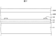
- FIG. 7 is a cross-sectional view showing a state in which an organic EL array layer 150 that is a layer forming the organic EL display device as shown in FIG.
- the organic EL array layer 150 in FIG. 7 is a layer including the organic base film 101 to the protective layer 115, as shown in FIG.
- the polyimide substrate 100 and the mother substrate 10 need to be stably bonded. This adhesive force is mainly maintained by the polyimide substrate 100 and the third layer 14 formed on the mother substrate 10.
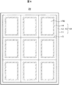
- FIG. 8 is a plan view showing the mother panel 20 in which a plurality of organic EL display devices are formed on the mother substrate 10.
- the organic EL display device is represented by the organic EL array layer 150.
- the third layer (second adhesive layer) 14 that acts as the main adhesive force between the polyimide substrate 100 and the mother substrate 10 is shown by a dotted line.
- solid lines 15 indicate boundaries of individual organic EL display devices.
- the individual organic EL display devices are separated from the mother panel by dicing or the like.
- the third layer 14 formed on the mother substrate 10 is formed slightly inside the separation line 15, for example, within a range of about 5 mm from the end.
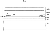
- FIG. 9 is a cross-sectional view showing a state where individual organic EL display devices are separated from the mother panel 20 of FIG.
- the glass substrate 31 is in a state of being cut out from the mother glass substrate 11 to the size of each organic EL display device.
- the first layer 12, the second layer 13, and the third layer 14 are formed on the glass substrate 31.
- the first layer 12 and the second layer 13 are formed on the entire surface, but the third layer 14 is formed in a frame shape along the inner circumference of the organic EL display device with a width w.
- a polyimide substrate 100 is formed so as to cover the second layer 13 and the third layer 14, and an organic EL array layer 150 is formed thereon. Of these, the polyimide substrate 100 and the organic EL array layer 150 form an organic EL display device. Then, the glass substrate 31, the first layer 12, the second layer 13, and the third layer 14 need to be separated from the polyimide substrate 100.
- the feature of the present invention is that the adhesion between the polyimide substrate 100 and the mother substrate 10 or the glass substrate 31 is mainly maintained by the third layer 14.
- the end portions are often separated from the glass substrate 31 side.
- peeling at the end portion occurs when the individual organic EL display devices are separated from the mother panel 20 by dicing or the like, and the mother panel 20 does not have this peeling during the manufacturing process. Since such peeling has not occurred, there is no problem.
- the organic EL display device is peeled off from the glass substrate 31, for example, manually by using the peeling portion at the end as shown in FIG.
- FIG. 10 is a cross-sectional view showing a state where the organic EL display device including the polyimide substrate 100 and the organic EL array layer 150 is peeled off from the glass substrate 31.
- SiN is used as the first layer 12
- Cu is used as the second layer 13
- AlO is used as the third layer 14.
- the glass substrate 31 and the SiN film 12 are firmly bonded.
- the Cu film 13 is firmly adhered to the SiN film 12.
- the Cu film 13 has a weak adhesion to the polyimide substrate 100. Therefore, the polyimide substrate 100 is easily separated from the second layer 13 made of Cu.
- the patterned third layer 14 is formed of AlO, and the adhesive force between the AlO film 14 and the polyimide substrate 100 is strong. Therefore, when the mother substrate 10 passes through the manufacturing process, most of the adhesive force of the polyimide substrate 100 to the mother substrate 10 is maintained by the third layer 14. On the other hand, the adhesion between the AlO film 14 and the Cu film 13, which is the second layer 13, is strong. Since the adhesive force between the AlO film 14 and the Cu film 13 is stronger than the adhesive force between the AlO film 14 and the polyimide substrate 100, even when the polyimide substrate 100 is peeled off from the AlO film 14, the AlO film 14 is formed by the Cu film 13 The bond with is maintained. Therefore, the polyimide substrate 100 is separated from the AlO film 14.
- the adhesive force between the third layer 14 and the polyimide substrate 100 is too strong, it cannot be peeled off. If it is too weak, there is a risk that the polyimide substrate 100 may be separated from the mother substrate 10 during the manufacturing process.
- the adhesive strength is evaluated by 90° peel strength according to ASTM (American Society for Testing and Material) D1876-01 standard, the adhesive strength between the polyimide substrate and the Cu film as the second layer is 0.01 to 0. It is 0.1 N/cm.
- the adhesive force between the polyimide substrate and the AlO film as the third layer is 2 to 4 N/cm, which is 40 to 200 times the adhesive force between the polyimide and Cu.
- An advantage of the present invention is that the adhesive force between the polyimide substrate 100 and the mother substrate 10 can be easily controlled by controlling, for example, the width of the third layer 14. If the patterning of the third layer 14 is the same, the adhesive force is considered to be proportional to the width of the third layer 14, so if the width w of the third layer 14 can be changed from about 0.1 mm to about 5 mm, it will be 1 time.
- the adhesive strength can be controlled to 50 times.
- the planar shape of the third layer 14 can be freely changed. Therefore, various shapes can be formed in consideration of the adhesive force in the process and the ease of peeling in the peeling process.
- the first layer 12, the second layer 13, and the third layer 14 do not remain in the organic EL display device after peeling. Therefore, since the influence of these layers is not visually observed, the commercial value is not spoiled apparently. However, microscopically, traces of this process remain on the bottom surface of the polyimide substrate 100.
- FIG. 11 is a rear view of the completed organic EL display device viewed from the polyimide substrate 100 side.
- the frame-shaped portion shown by the dotted line in FIG. 11 is the place where the third layer 14 was present in the mother substrate 10. Further, this place is a portion where the third layer 14 exists on the glass substrate 31 in FIG. 9. Since the third layer 14 has a thickness of 10 nm to 50 nm, there is no change in appearance when viewed from the polyimide substrate 100 having a thickness of 10 ⁇ m to 20 ⁇ m. However, microscopically, the concave portion of the portion where the third layer 14 was present is present.
- the third layer 14 is rough on the polyimide substrate 100 side due to the strong peeling. Face 160 is created. That is, the roughness of the back surface of the polyimide substrate 100 at the portion where the third layer 14 and the polyimide substrate 100 contact each other is larger than the roughness when the second layer 13 and the polyimide substrate 100 contact each other.
- the surface roughness is stipulated in JIS standard, and there are parameters such as Ra, Rz, and Rms, but any of them may be used for comparison.
- the surface roughness can be measured using a surface roughness meter such as Surfcom or an atomic force microscope (AFM).
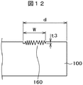
- FIG. 12 is a schematic sectional view corresponding to the BB sectional view of FIG. 11.
- a portion where the polyimide substrate 100 was in contact with the third layer 14 of the mother substrate 10 was formed with a recess by a thickness t3, and a rough surface 160 was formed in the recess.
- the rough surface 160 is formed when the polyimide substrate 100 is peeled off from the third layer 14. Ra of the rough surface in the recess is larger than the depth of the recess.
- the inner portion of the frame-shaped portion shown by the dotted line in FIG. 11 is the place where the second layer 13 of the mother substrate 10 was present.
- This portion is a portion where the second layer 13 and the polyimide substrate 100 are in contact with each other, and the components of the second layer 13 diffuse into the polyimide substrate 100 during the process, leaving a trace such as a deposit.
- Cu copper
- Cu atoms are diffused in the polyimide substrate 100 and bonded with oxygen contained in the polyimide substrate 100 to precipitate copper oxide.
- TEM transmission electron microscope
- 11 and 12 d is the distance between the polyimide substrate 100 and the third layer 14 of the mother substrate 10, that is, the distance from the inside of the rough surface 160 to the edge of the polyimide substrate 100.
- the value of d is usually 5 mm or less.
- the organic EL display device shown in FIG. 9 has a total thickness of 20 ⁇ m to 30 ⁇ m of the polyimide substrate 100 and the organic EL array layer 150, and since it has no rigidity, it may be difficult to handle in the process after peeling the glass substrate 31.
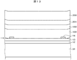
- the supporting resin substrate 200 may be attached on the organic EL array layer 150 via the adhesive material 201.
- FIG. 13 is a sectional view showing the configuration in this case.
- FIG. 13 is a cross-sectional view showing a state in which each organic EL display device is cut out from the mother panel 20 by dicing or the like. Even in such a case, the relationship between the first layer 12, the second layer 13, and the third layer 14 formed on the TFT substrate 100 and the glass substrate 30 is the same.
- the supporting resin substrate 200 can have a thickness of, for example, about 100 ⁇ m.
- FIG. 14 shows a state in which the organic EL display device is peeled off from the glass substrate 31 from the state of FIG. This operation is the same as the peeling step described with reference to FIG. As shown in FIG. 14, after peeling, the supporting resin substrate 200 is peeled off if necessary.
- a circularly polarizing plate may be arranged on the organic EL array layer 150 to suppress reflection of external light. This circularly polarizing plate can also serve the role of the supporting resin substrate 200.
- 15 to 20 are plan views showing an example of the shape of the third layer 14 formed on the mother substrate 10.
- 15 to 20 describe the glass substrate 31 of each organic EL display device, the same applies to the case of the mother substrate 10. 15 to 20, it is common that the first layer 12 and the second layer 13 are formed on the entire surface of the glass substrate 31.
- the difference between FIGS. 15 to 20 is the shape of the third layer 14.
- the materials of the first layer 12, the second layer 13, and the third layer 14 are as described with reference to FIG.
- the adhesive force between the third layer 14 and the polyimide substrate 100 can be freely determined not only by the width of the third layer 14 but also by the planar shape of the third layer 14.
- the adhesion between the third layer 14 and the polyimide substrate 100 needs to balance the adhesive force in the manufacturing process and the ease of peeling in the peeling process, but in the present invention, the shape of the third layer 14 is changed.
- the adhesive force can be controlled also by this, so that there is a large degree of freedom.
- the third layer 14 is formed along the side of the organic EL display device, but the third layer 14 is not a closed curve, and there is a portion where only the gap g1 is opened at the corner. Due to the existence of the gap g1, when the organic EL display device is separated from the mother panel 20 by dicing or the like, a peeling portion is apt to occur between the polyimide substrate 100 and the glass substrate 31 at the corner portion, and this portion is removed.
- the organic EL display device including the polyimide substrate 100 as a starting point can be easily peeled off from the glass substrate 31.
- this portion becomes an abnormal point, but since the thickness of the third layer 14 is 10 nm to 50 nm and the thickness of the polyimide substrate 100 is 10 ⁇ m to 20 ⁇ m, this abnormal point is present. Does not really matter. The same applies to the cases of FIGS. 16 to 20.
- FIG. 16 shows a case in which, in the third layer 14, in addition to the gap g1 at the corner portion, the gap g2 is formed at the side portion.
- the gap g2 can balance the adhesive force and the ease of peeling.
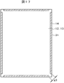
- FIG. 17 is an example in which the third layer 14 is formed along the edge of the side of the glass substrate 31.
- the gap g3 is formed at the corner portion to remove the polyimide substrate 100 from the corner portion. It can be peeled off from the glass substrate 31.
- FIG. 18 is the same as FIG. 17 in that the third layer 14 is formed up to the edge of the side of the glass substrate 31, but the gap g2 and the gap g3 are arranged only on one side. Thereby, the edge of the polyimide substrate 100 can be easily peeled off from the glass substrate 31 always on a specific side. Then, with this portion as a starting point, the polyimide substrate 100 and the glass substrate 31 are separated.
- the third layer 14 in the present invention exists on the glass substrate 39 side and does not remain on the polyimide substrate 100 side after the polyimide substrate 100 is separated from the glass substrate 31. Microscopically or by analysis, traces of the third layer 14 remain, but they cannot be visually recognized. Therefore, the third layer 14 can also be formed in a region corresponding to the display region. Since the third layer 14 can be formed in the area corresponding to the display area, the degree of freedom in adjusting the adhesive force between the polyimide substrate 100 and the glass substrate 31 becomes very large.
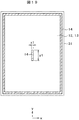
- FIG. 19 shows an example in which the third layer 14 is formed over a width x1 and a length y1 in a portion corresponding to substantially the center of the display area of the organic EL display device.
- x1 and y1 it is possible to balance the adhesive force and the ease of peeling.
- FIG. 20 is an example in which the third layer 14 is formed over a width y2 and a length x2 in a portion corresponding to substantially the center of the display area of the organic EL display device.
- x2 and y2 it is possible to balance the adhesive force and the ease of peeling.
- the third layer 14 can be formed in various positions corresponding to the display area and in various sizes and shapes. Further, a plurality of third layers can be formed in the portion corresponding to the display area.
Landscapes
- Engineering & Computer Science (AREA)
- Chemical & Material Sciences (AREA)
- Manufacturing & Machinery (AREA)
- Chemical Kinetics & Catalysis (AREA)
- Life Sciences & Earth Sciences (AREA)
- General Chemical & Material Sciences (AREA)
- Geochemistry & Mineralogy (AREA)
- Materials Engineering (AREA)
- Organic Chemistry (AREA)
- Ceramic Engineering (AREA)
- Physics & Mathematics (AREA)
- General Physics & Mathematics (AREA)
- Theoretical Computer Science (AREA)
- Microelectronics & Electronic Packaging (AREA)
- Electroluminescent Light Sources (AREA)
- Devices For Indicating Variable Information By Combining Individual Elements (AREA)
Abstract
樹脂基板を有するフレキシブル表示装置を高歩留まりで製造することを目的とする。このために、本発明は次のような構成を有する。すなわち、樹脂基板100を有する表示装置の製造方法であって、ガラス基板31上に金属または金属酸化物からなる第1層12を形成し、前記第1層12の上に金属または金属酸化物からなる第2層13を形成し、前記第2層13の上に金属または金属酸化物からなる第3層14を形成し、前記第3層14をパターニングし、前記第3層14の上に樹脂基板100を形成し、前記樹脂基板の上に画像を形成するための層を形成し、その後、前記樹脂基板100を、前記第2層13および第3層14の層から剥離することを特徴とする表示装置の製造方法である。
Description
本発明は表示装置に係る、湾曲させることができるフレキシブル基板及びその製造方法に関する。
有機EL表示装置や液晶表示装置は表示装置を薄くすることによって、湾曲させて使用することができる。また、基板をポリイミド等の樹脂によって形成することでフレキシブルな表示装置とすることができる。有機EL表示装置はバックライトが不要な分、薄型表示装置としては有利である。
基板を10μm乃至20μm程度の薄い樹脂で形成した場合、表示装置としてはフレキシブルなものとなるが、製造工程を通すことは難しい。そこで、表示装置の製造工程においては、厚さ0.5mmあるいは0.7mm程度のガラス基板の上に樹脂基板を形成し、その上に表示素子を形成する。そして、表示装置が完成後、ガラス基板と樹脂基板の界面にレーザを照射し、樹脂にアブレーションを生じさせて、ガラス基板と樹脂基板を分離することが行われている。
特許文献1には、レーザを用いてガラス基板と樹脂基板を分離する技術が記載されている。
レーザを用いた剥離方法は、レーザ装置が高コストであること、また、ガラス基板と樹脂基板との界面に正確にレーザ照射を行うための制御が難しく、製造歩留りの点で課題が存在する。
特許文献2及び特許文献3には、レーザを用いず、ガラス基板と樹脂基板をはく離する方法として、次のような方法が提案されている。すなわち、ガラス基板に樹脂基板と容易に剥離する剥離層を、樹脂基板の周辺部分に対応する部分以外に形成しておく。樹脂基板の周辺において、樹脂基板とガラス基板が強く接着しており、製造工程中は、樹脂基板とガラス基板の接着を維持する。その後、最終工程において、樹脂基板のガラス基板と接着した部分を切り離す。そうすると、樹脂基板は剥離層とのみ接着していることになるので、樹脂基板はガラス基板から容易に離すことが出来る。上記の特許文献の内、特許文献3には、さらに、ガラス基板を再生して使うことが出来る構成が記載されている。
特許文献2、特許文献3のいずれも樹脂基板とガラス基板が接着した部分を残すようにマザー基板をレイアウトする必要があり、材料歩留り的には、課題がある。
本発明の課題は、レーザ装置を用いることなく、また、材料歩留りを上げることが可能で、かつ、高価な設備を必要としない有機EL表示装置の製造方法を実現することである。
本発明は上記課題を克服するものであり、代表的な手段は次のとおりである。
(1)樹脂基板を有する表示装置であって、前記樹脂基板は、画像表示のための層が形成された表面と、前記表面とは裏側の、裏面を有し、前記裏面は周辺領域と、前記周辺領域よりも内側の内側領域を有し、前記周辺領域には、前記内側領域よりも粗面になっている領域が形成されていることを特徴とする表示装置。
(2)樹脂基板を有する表示装置の製造方法であって、ガラス基板上に金属または金属酸化物からなる第1層を形成し、前記第1層の上に金属または金属酸化物からなる第2層を形成し、前記第2層の上に金属または金属酸化物からなる第3層を形成し、前記第3層をパターニングし、前記第3層の上に樹脂基板を形成し、前記樹脂基板の上に画像を形成するための層を形成し、その後、前記樹脂基板を、前記第2層および第3層の層から剥離することを特徴とする表示装置の製造方法。
以下に実施例を用いて本発明の内容を詳細に説明する。実施例は有機EL表示装置について説明しているが、本発明は、液晶表示装置等、樹脂基板を用いた他の表示装置にも適用することが出来る。
図1は本発明が適用される有機EL表示装置の平面図である。本発明の有機EL表示装置は、フレキシブルに湾曲させることが出来る表示装置である。したがって、TFT(Thin Film Transistor)、走査線、電源線、映像信号線、画素電極、有機EL発光層等が形成されているTFT基板100は樹脂で形成されている。
図1において、表示領域90の両側には走査線駆動回路80が形成されている。表示領域90には、横方向(x方向)に走査線91が延在し、縦方向(y方向)に配列している。映像信号線92及び電源線93が縦方向に延在し、横方向に配列している。走査線91と、映像信号線92及び電源線93で囲まれた領域が画素95となっており、画素95内には、TFTで形成された駆動トランジスタ、スイッチングトランジスタ、光を発光する有機EL発光層等が形成されている。
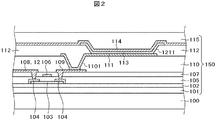
図2は図1に示す有機EL表示装置の表示領域の断面図である。図2において、TFT基板100は樹脂で形成されている。樹脂の中でもポリイミドは、耐熱性、機械的強度等から、表示装置の基板としては優れた特性を有している。したがって、以後は、TFT基板100を構成する樹脂としては、ポリイミドを前提として説明するが、本発明は、ポリイミド以外の樹脂でTFT基板100を構成した場合にも適用することが出来る。なお、本明細書では、TFT基板100をポリイミド基板100と呼ぶこともある。TFT基板100の厚さは例えば10乃至20μmである。
ポリイミド基板100の上には、表面をさらに平坦化するためのポリイミド膜101が2乃至3μmの厚さで形成されている。ポリイミド膜101の上に、有機EL層に樹脂基板100から水分や不純物が侵入することを防止するための無機下地膜102が形成されている。無機下地膜102の上にスイッチングTFTを構成する酸化物半導体103が形成されている。酸化物半導体103のドレイン部及びソース部には、酸化物半導体103を保護するための、接続電極104がTiあるいはMoW等で形成されている。
酸化物半導体103を覆ってゲート絶縁膜105が形成され、ゲート絶縁膜105の上にゲート電極106が形成されている。ゲート電極106を覆って層間絶縁膜107が形成され、層間絶縁膜107の上にドレイン電極108とソース電極109が形成される。ドレイン電極108は酸化物半導体103と映像信号線92とを接続している。ソース電極109は酸化物半導体103と有機EL層113のための下部電極111と接続している。
ドレイン電極108及びソース電極109を覆って有機パッシベーション膜112が2乃至3μmの厚さで形成される。有機パッシベーション膜110には、ポリイミド、アクリル等が使用される。有機パッシベーション膜110にはスルーホール1101が形成され、ソース電極109と下部電極111を接続することを可能にしている。下部電極111は、下層が金属である反射電極で、上層が陽極となるITO(Indium Tin Oxide)で形成されている。
下部電極111の周辺を覆ってバンク112が形成されている。バンク112は、ポリイミドあるいはアクリル等の樹脂によって表示領域全面に形成された後、下部電極111に対応する部分にホール1121を形成する。ホール1121とホール1121の間がバンク112となる。ホール1121内に発光素子となる有機EL層113を形成し、その上にカソードとなる上部電極114が、ITO(Indium、Tin、Oxide)等の透明導電膜によって形成される。上部電極113は表示領域全面に形成される。
上部電極114の上に、有機EL層113を外部からの水分等から保護するための、保護膜115が形成される。保護膜115は、例えば、SiN等の無機膜及びポリイミドあるいはアクリル等の有機膜の積層膜によって形成される。
図1及び図2で説明した有機EL表示装置は厚さが10乃至20μmの、ポリイミド等の樹脂で形成された基板100に形成されているので、非常にフレキシブルな表示装置である。このような薄い樹脂基板100を有する有機EL表示装置は、次のような製造方法によって形成される。
有機EL表示装置を多数形成することが出来るマザーガラス基板の表面にポリアミック酸を含むポリイミドの原料をスリットコータ等で塗布する。ポリイミド材料は、例えば、東レ製の「セミコファインSP-020」であり、具体的な成分は、N-メチルピロドリン85%、ポリアミック酸15%である。このうち、ポリアミック酸がイミド化し、ポリイミドとなる。この材料を例えば、焼成後、厚さが10μm程度になるように塗布してTFT基板100を形成する。
このポリイミドによるTFT基板100の上に、図2で述べたような層を形成し、有機EL表示装置を形成する。この状態は、マザーガラス基板の上に多数の有機EL表示装置が形成された状態である。本明細書では、これをマザーパネルと呼ぶ。その後、マザーパネルから個々の有機EL表示装置を分離し、さらに、樹脂基板を含む有機EL表示装置からガラス基板を剥離する。本発明は、ガラス基板と樹脂基板の剥離方法に特徴がある。
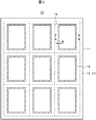
図3は、本発明によるマザー基板10の平面図であり、マザーガラス基板11の上に、有機EL表示装置とガラス基板とを剥離するための、3層の金属層が形成された状態である。マザー基板10の上に多数の有機EL表示装置が形成されることになる。本明細書では、多数の有機EL表示装置が形成されていることになる大型のガラス基板をマザーガラス基板11と言い、マザーガラス基板11の上に剥離のための3層の金属層が形成された状態をマザー基板10とよび、マザー基板10の上に多数の有機EL表示装置が形成された状態をマザーパネル20と呼ぶ。
図3において、マザーガラス基板11の上に、金属あるいは金属酸化物からなる、第1層12、第2層13、第3層14が形成されている。なお、金属という場合は、合金も含む意味である。マザーガラス基板11側から、第1層12及び第2層13はマザーガラス基板11全面に平面状に形成される。図3において、点線は、マザー基板10の上に多数の有機EL表示装置が形成された後のマザーパネル20から、個々の有機EL表示装置が分離される線を示している。第3層14は、個々の有機EL表示装置の周辺部に沿って枠状に形成されている。
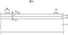
図4は図3のA-A断面図である。図4において、マザーガラス基板11の上に第1層12が平面状に形成され、その上に第2層13が平面状に形成され、その上に第3層14が細いストライプ状に形成されている。第1層12と第2層13はマザーガラス基板11の全面に形成される。第3層14は全面に形成された後、エッチング等によってパターニングされる。
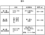
本明細書では、第1層12を第1接着層ともいう。第1層12は、下層のガラス基板11、上層の第2層13とのいずれとも、強い接着力を有する。図5に示すように、第1層12の材料としては、SiN、ITO、AlO等が使用される。第1層12は、例えばスパッタリングによって形成され、厚さt1は、50nm乃至100nm程度である。
第1層12とガラス基板11の接着力、及び、第1層12と第2層13との接着力は、後に、有機EL表示装置を第2層13及び第3層14から引き剥がすときの剥離強度よりも強い。言い換えると、有機EL表示装置の第2層13の接着力と第3層14の接着力の合計は、ガラス基板11と第1層12の接着力、及び、第1層12と第2層13との接着力よりも小さい。
第2層13は第1層12の上にマザーガラス基板11の全面を覆って形成される。本明細書では、第2層13は剥離層とも呼ぶ。第2層13は、下地である第1層12とは強い接着力を有するが、上に形成される樹脂基板100とは弱い接着力を有し、樹脂基板100は第2層から容易に引き剥がすことが出来る。図5に示すように、第2層13の材料としては、Cu、CuO、Mg、MgO、Ni、NiO、Au等が使用される。第2層13は、例えばスパッタリングによって形成され、厚さt2は、50nm乃至100nm程度である。
第3層14は第2層13の上に、個々の有機EL表示装置の周辺部に対応する部分に、枠状に形成される。第3層14は、まず、第2層13の上において、マザーガラス基板11全面を覆うように形成され、その後、エッチングによってパターニングする。第3層14は、第2層13とポリイミド基板100との双方に対して強い接着力を有するが、第3層14と第2層13の接着力のほうが第3層14とポリイミド基板100との接着力よりも強い。有機EL表示装置を剥離したときに、第3層14を第2層13上に残留させるためである。
図5に示すように、第3層14の材料としては、AlO、SiN、ITO、Cr、Ti等が使用される。第3層14は、例えばスパッタリングによって形成され、厚さt3は、10nm乃至50nm程度である。第3層14は、製造工程において、ポリイミド基板100をマザーガラス基板11に保持する役割があるので、ポリイミド基板100との接着力は必要であるが、この接着力は、第3層14の線幅wによっても影響される。線幅は例えば、0.1mmから5mm程度である。
図6は、図3及び図4に示すマザー基板10に有機EL表示装置用のTFT基板100、すなわち、ポリイミド基板100を形成した状態を示す断面図である。ポリイミド基板100は、図2で説明したような塗布方法によって、焼成後の厚さが10μm乃至20μmになるように形成される。このポリイミド基板100の上に、図2で示すように、有機下地膜101、TFT層、有機EL層113、保護膜115等が順番に成される。
図7は、ポリイミド基板100の上に、図2に示すような有機EL表示装置を構成する層である有機ELアレイ層150を形成した状態を示す断面図である。図7の有機ELアレイ層150は、図2に示すように、有機下地膜101から保護層115を含む層をいう。製造工程を通過する間、ポリイミド基板100とマザー基板10とは安定に接着している必要がある。この接着力は、主に、ポリイミド基板100とマザー基板10に形成された第3層14によって維持される。
図8は、マザー基板10に複数の有機EL表示装置を形成した状態のマザーパネル20を示す平面図である。図8において、有機EL表示装置は、有機ELアレイ層150によって表されている。また、ポリイミド基板100とマザー基板10の間の主たる接着力として作用する第3層(第2接着層)14が点線で示されている。
図8において、実線15は、個々の有機EL表示装置の境界を示す。この線において、ダイシング等によって、個々の有機EL表示装置がマザーパネルから分離される。マザー基板10に形成された第3層14は分離線15よりも若干内側、例えば端部から5mm程度範囲内に形成されている。
図9は、図8のマザーパネル20から個々の有機EL表示装置を分離した状態を示す断面図である。図9においてガラス基板31は、マザーガラス基板11から個々の有機EL表示装置の大きさに切り出された状態である。ガラス基板31の上に第1層12、第2層13、第3層14が形成されている。第1層12、第2層13は全面に形成されているが、第3層14は、幅wで有機EL表示装置の内周に沿って枠状に形成されている。
第2層13、第3層14を覆ってポリイミド基板100が形成され、その上に有機ELアレイ層150が形成されている。このうち、ポリイミド基板100と有機ELアレイ層150が有機EL表示装置となる。そして、ガラス基板31、第1層12、第2層13、第3層14はポリイミド基板100から剥離する必要がある。
本発明の特徴は、ポリイミド基板100とマザー基板10あるいはガラス基板31との接着は主に、第3層14によって維持されていることである。そして、ポリイミド基板100の大部分の面と接触している第2層13は、ポリイミド基板100との接着力が弱く、容易に剥離する。例えば、図9の矢印で示すように、ダイシング等によって、個々の有機EL表示装置をマザーパネル20から分離する際、端部がガラス基板31側から剥離することが多い。但しこのような端部での剥離は、ダイシング等によって、個々の有機EL表示装置を、マザーパネル20から分離する際に生ずるものであって、製造工程を通る間は、マザーパネル20にはこのような剥離は生じていないので、問題はない。
本発明では、図9に示すような、端部の剥離部を利用して、例えば人手によって、ガラス基板31から有機EL表示装置を引き剥がす。この様子を図10に示す。図10は、ポリイミド基板100と有機ELアレイ層150からなる有機EL表示装置をガラス基板31から引き剥がしている状態を示す断面図である。
図10では、第1層12としてSiNを用い、第2層13としてCuを用い、第3層14としてAlOを用いた例である。図10において、ガラス基板31とSiN膜12は強固に接着している。Cu膜13はSiN膜12と強固に接着している。しかし、Cu膜13はポリイミド基板100との接着力は弱い。したがって、ポリイミド基板100は、Cuで形成された第2層13とは容易に剥離する。
パターニングされた第3層14はAlOで形成され、AlO膜14とポリイミド基板100との接着力は強い。したがって、マザー基板10が製造工程を通過するときは、ポリイミド基板100のマザー基板10への接着力は大部分が第3層14によって維持されている。一方、AlO膜14と第2層13であるCu膜13との接着は強固である。AlO膜14とCu膜13との接着力は、AlO膜14とポリイミド基板100との接着力よりも強いので、ポリイミド基板100をAlO膜14から剥離するときも、AlO膜14は、Cu膜13との接着は維持している。したがって、ポリイミド基板100はAlO膜14から剥離される。
ここで、第3層14とポリイミド基板100の接着力は、強すぎると、剥離できなくなる。また、弱すぎると製造工程中にポリイミド基板100がマザー基板10から剥離する危険がある。接着力をASTM(American Society for Testing and Material) D1876-01規格に準拠した、90°ピール強度で評価した場合、ポリイミド基板と第2層であるCu膜との接着力は、0.01乃至0.1N/cmである。一方、ポリイミド基板と第3層であるAlO膜との接着力は2乃至4N/cmであり、ポリイミドとCuの接着力の40乃至200倍である。
したがって、ポリイミド基板100とガラス基板31あるいはマザー基板10との接着力の大部分はポリイミド基板100と第3層14との接着力によって維持されている。本発明の優れた点は、第3層14の例えば、幅をコントロールすることによって、簡単にポリイミド基板100とマザー基板10の接着力を制御できるということである。第3層14のパターニングが同一であれば接着力は、第3層14の幅に比例すると考えられるので、第3層14の幅wを0.1mmから5mm程度まで変化出来るとすると、1倍から50倍の接着強度に制御することが出来る。
さらに、第3層14は、エッチングによってパターニングされるので、第3層14の平面形状は自由に変化させることが出来る。したがって、工程中での接着力、ピーリング工程における剥離のし易さを考慮して色々な形状とすることが出来る。
このように、剥離後の有機EL表示装置には、第1層12、第2層13、第3層14とも残っていない。したがって、目視では、これらの層の影響は見られないので、外見上商品価値を損なうことはない。しかし、微視的にみると、ポリイミド基板100の底面には、本プロセスの痕跡は残っている。
図11は、完成した有機EL表示装置をポリイミド基板100側から視た裏面図である。図11において点線で示した枠状の部分がマザー基板10における第3層14が存在していた場所である。また、この場所は、図9において、ガラス基板31の上に第3層14が存在している部分である。第3層14は厚さ10nm乃至50nmであるので、厚さ10μm乃至20μmのポリイミド基板100から視たら、外見上は、全く変化は無い。しかし、微視的には、第3層14が存在していた部分の凹部は存在している。
さらにこの第3層14は、ポリイミド基板100との接着力が第2層13のポリイミド基板100との接着力よりも格段に大きいので、ポリイミド基板100側に、強い力で引き剥がしたことによる粗面160が生ずる。つまり、第3層14とポリイミド基板100が接触した部分のポリイミド基板100の裏面の粗さは、第2層13とポリイミド基板100が接触した時の粗さよりも大きくなっている。
表面粗さは、JIS規格に規定されており、Ra、Rz、Rms等のパラメータがあるが、そのいずれを用いて比較してもよい。表面粗さは、サーフコム等の表面粗さ計または原子間力顕微鏡(AFM)を用いて測定することができる。
但し、表面粗さ計では、第3層14の厚さである10nm乃至50nmの凹凸の測定は困難である。また、粗面の度合いが小さい場合も表面粗さ計では測定は困難である。このような場合も、走査型電子顕微鏡(SEM)あるいは、透過型電子顕微鏡(TEM)を用いることによって測定可能である。
図12は、図11のB-B断面図に相当する断面模式図である。図12において、ポリイミド基板100がマザー基板10の第3層14と接触していた部分は、厚さt3だけ凹部が形成され、その凹部の中にラフな面160が形成されている。ラフな面160は、ポリイミド基板100を第3層14から引き剥がす時に形成されたものである。凹部の中の粗面のRaは凹部の深さよりも大きい。
また、図11において点線で示した枠状の部分の内側の部分はマザー基板10における第2層13が存在していた場所である。この部分は第2層13とポリイミド基板100が接触していた部分であり、工程中に第2層13の成分がポリイミド基板100に拡散し、析出物等の痕跡を残す。例えば、第2層13にCu(銅)を用いた場合、ポリイミド基板100中にCuの原子が拡散し、ポリイミド基板100中に含まれる酸素と結合し銅の酸化物が析出する。この析出物等は透過型電子顕微鏡(TEM)により観察可能であり、電子線、X線等による成分分析によっても測定することができる。
図11及び図12のdは、ポリイミド基板100にマザー基板10の第3層14が接触した部分、すなわち、ラフな面160の内側からポリイミド基板100の端部までの距離である。dの値は、通常は5mm以下である。
図9に示す有機EL表示装置はポリイミド基板100と有機ELアレイ層150を合計しても20μm乃至30μmであり、剛性が無いのでガラス基板31を剥離した後の工程において扱いにくい場合がある。この対策として、有機ELアレイ層150上に粘着材201を介して支持樹脂基板200を取り付ける場合がある。
図13はこの場合の構成を示す断面図である。図13は、マザーパネル20から個々の有機EL表示装置をダイシング等によって切り出した状態を示す断面図である。このような場合であっても、TFT基板100とガラス基板30の上に形成された第1層12、第2層13、第3層14の関係は同じである。支持樹脂基板200の厚さは、例えば、100μm程度にすることが出来る。
図14は、図13の状態から、有機EL表示装置をガラス基板31から引き剥がしている状態である。この動作は、図10で説明した剥離工程と同じである。図14のように、剥離をした後、支持樹脂基板200は必要に応じて剥離される。ところで、有機EL表示装置においても、外光の反射は、画像を著しく劣化させる。そこで、有機ELアレイ層150の上に円偏光板を配置して、外光の反射を抑える場合がある。支持樹脂基板200の役割をこの円偏光板によって兼用させることも出来る。
図15乃至図20はマザー基板10に形成される第3層14の形状の例を示す平面図である。図15乃至図20は個々の有機EL表示装置のガラス基板31について説明するが、マザー基板10の場合も同じである。そして、図15乃至図20はガラス基板31の上、全面に第1層12と第2層13が形成されていることは共通である。図15乃至図20で異なる点は、第3層14の形状である。なお、第1層12、第2層13、第3層14の材料は図5等で説明したとおりである。
本発明では、第3層14とポリイミド基板100との接着力は、第3層14の幅のみでなく、第3層14の平面形状によっても自由に決めることが出来る。第3層14とポリイミド基板100との接着は、製造工程における接着力と、剥離工程における剥離のし易さとのバランスをとる必要があるが、本発明では、第3層14の形状を変化させることによっても、接着力を制御できるので、大きな自由度を有している。
図15は、第3層14は有機EL表示装置の辺に沿って形成されているが、第3層14は閉曲線ではなく、コーナー部において、ギャップg1だけ解放されている箇所がある。このギャップg1の存在によって、ダイシング等によって、有機EL表示装置をマザーパネル20から分離したときに、コーナー部において、ポリイミド基板100とガラス基板31との間に剥離箇所が生じやすくなり、この部分を起点にしてポリイミド基板100を含む有機EL表示装置をガラス基板31から引き剥がし易くなる。
なお、解放箇所g1が存在している場合、この部分は異常点になるが、第3層14の膜厚が10nm乃至50nmであり、ポリイミド基板100の厚さは10μm乃至20μmなので、この異常点が実際に問題になることは無い。図16乃至図20の場合も同様である。
図16は、第3層14において、コーナー部におけるギャップg1に加え、辺部にギャップg2を形成した場合である。ギャップg2によって、接着力と剥離のし易さのバランスをとることが出来る。
図17は、第3層14をガラス基板31の辺の端部に沿って形成した例である。但し、全周にわたって第3層14を辺の端部に形成すると、ポリイミド基板100とガラス基板31の剥離が困難になるので、コーナー部にギャップg3を形成して、コーナー部からポリイミド基板100をガラス基板31から剥離できるようにしている。
図17は、第3層14をガラス基板31の辺の端部に沿って形成した例である。但し、全周にわたって第3層14を辺の端部に形成すると、ポリイミド基板100とガラス基板31の剥離が困難になるので、コーナー部にギャップg3を形成して、コーナー部からポリイミド基板100をガラス基板31から剥離できるようにしている。
図18は、第3層14をガラス基板31の辺の端部にまで形成していることは図17と同じであるが、ギャップg2、ギャップg3を1辺側にのみ配置している。これによって、常に特定の辺において、ポリイミド基板100の端部がガラス基板31から剥離しやすくすることが出来る。そして、この部分を起点にしてポリイミド基板100とガラス基板31を剥離する。
本発明における第3層14は、ポリイミド基板100をガラス基板31から剥離した後は、ガラス基板39側に存在し、ポリイミド基板100側には残らない。顕微鏡的には、あるいは、分析をすれば、第3層14の痕跡は残るが、目視では認識できない。したがって、第3層14は表示領域と対応する領域にも形成することが出来る。表示領域と対応する領域にも、第3層14を形成できることによって、ポリイミド基板100とガラス基板31との接着力を調整する自由度は非常に大きくなる。
図19は、有機EL表示装置の表示領域のほぼ中央に対応する部分に幅x1、長さy1にわたって第3層14を形成した例である。x1とy1によって、接着力と剥離のし易さのバランスをとることが出来る。図20は、有機EL表示装置の表示領域のほぼ中央に対応する部分に幅y2、長さx2にわたって第3層14を形成した例である。x2とy2によって、接着力と剥離のし易さのバランスをとることが出来る。
図19あるいは図20の形状に限らず、表示領域に対応する種々の位置に、また、種々の大きさ、形状に第3層14を形成することが出来る。また、表示領域に対応する部分に複数の第3層を形成することが出来る。
10…マザー基板、 11…マザーガラス基板、 12…第1層(第1接着層)、 13…第2層(剥離層)、 14…第3層(第2接着層)、15…切断線、16…AlOバリア層、 20…マザーパネル、 31…ガラス基板、 80…走査線駆動回路、 90…表示領域、 91…走査線、 92…映像信号線、 93…電源線、 95…画素、 100…TFT基板、 101…有機下地膜、 102…無機下地膜、 103…半導体層、 104…金属保護層、 105…ゲート絶縁膜、 106…ゲート電極、 107…層間絶縁膜、 108…ドレイン電極、 109…ソース電極、 110…有機パッシベーション膜、 111…下部電極、 112…バンク、 113…有機EL層、 114…上部電極、 115…保護膜、 150…有機ELアレイ層、 160…粗面、 200…支持樹脂基板、 201…粘着材、 400…フレキシブル配線基板、 1101…スルーホール、 1121…ホール
Claims (17)
- 樹脂基板を有する装置であって、
前記樹脂基板は、機能層が形成された表面と、前記表面に対して背面側の、裏面を有し、
前記裏面は周辺領域と、前記周辺領域よりも内側の内側領域を有し、
前記周辺領域には、前記内側領域よりも粗面になっている領域が形成されていることを特徴とする樹脂基板を有する装置。 - 前記粗面になっている領域は、前記樹脂基板の辺に沿って形成されていることを特徴とする請求項1に記載の樹脂基板を有する装置。
- 前記粗面になっている領域は、前記樹脂基板の端部から5mm以内に形成されていることを特徴とする請求項1に記載の樹脂基板を有する装置。
- 前記樹脂基板はポリイミド基板であることを特徴とする請求項1に記載の樹脂基板を有する装置。
- 樹脂基板を有する装置の製造方法であって、
ガラス基板上に金属または金属酸化物からなる第1層を形成し、
前記第1層の上に金属または金属酸化物からなる第2層を形成し、
前記第2層の上に金属または金属酸化物からなる第3層を形成し、
前記第3層をパターニングし、
前記第3層の上に樹脂基板を形成し、
前記樹脂基板の上に機能層を形成し、
その後、前記樹脂基板を、前記第2層および第3層の層から剥離することを特徴とする樹脂基板を有する装置の製造方法。 - 前記第3層の前記樹脂基板との接着力は、前記第2層と前記樹脂基板との接着力よりも強いことを特徴とする請求項5に記載の樹脂基板を有する装置の製造方法。
- 前記第2層の前記第1層との接着力は、前記第2層の前記ポリイミド基板との接着力よりも強いことを特徴とする請求項5に記載の樹脂基板を有する装置の製造方法。
- 前記第3層の前記第2層との接着力は、前記第3層の前記ポリイミド基板との接着力よりも強いことを特徴とする請求項5に記載の樹脂基板を有する装置の製造方法。
- 前記第1層の前記ガラス基板との接着力は、前記第3層の前記ポリイミド基板との接着力よりも強いことを特徴とする請求項5に記載の樹脂基板を有する装置の製造方法。
- 前記第1層は、SiN、ITO、AlOのいずれかであることを特徴とする請求項5に記載の樹脂基板を有する装置の製造方法。
- 前記第2層は、Cu、CuO、Mg、MgO、Ni、NiO、Auのいずれかであることを特徴とする請求項5に記載の樹脂基板を有する装置の製造方法。
- 前記第3層は、AlO、SiN、ITO、Cr、Tiのいずれかであることを特徴とする請求項5に記載の樹脂基板を有する装置の製造方法。
- 前記第1層は、SiNであり、前記第2層はNiであり、前記第3層はAlOであることを特徴とする請求項5に記載の樹脂基板を有する装置の製造方法。
- 前記樹脂基板はポリイミド基板であることを特徴とする請求項5に記載の樹脂基板を有する装置の製造方法。
- 前記ガラス基板は、周辺領域と、前記周辺領域の内側である、内側領域を有し、
前記第3層は、前記周辺領域に前記ガラス基板の辺に沿って形成されていることを特徴とする請求項5に記載の樹脂基板を有する装置の製造方法。 - 前記第3層は、前記周辺領域において、前記ガラス基板の4つの辺に沿って形成されていることを特徴とする請求項15に記載の樹脂基板を有する装置の製造方法。
- 前記第3層は、前記内側領域に、島状に形成されていることを特徴とする請求項15に記載の樹脂基板を有する装置の製造方法。
Priority Applications (2)
| Application Number | Priority Date | Filing Date | Title |
|---|---|---|---|
| CN202080014901.XA CN113424247B (zh) | 2019-02-19 | 2020-02-17 | 具有树脂基板的装置及其制造方法 |
| US17/391,518 US20210367172A1 (en) | 2019-02-19 | 2021-08-02 | Device having resin substrate and manufacturing method thereof |
Applications Claiming Priority (2)
| Application Number | Priority Date | Filing Date | Title |
|---|---|---|---|
| JP2019-027234 | 2019-02-19 | ||
| JP2019027234A JP7306835B2 (ja) | 2019-02-19 | 2019-02-19 | 樹脂基板を有する装置及びその製造方法 |
Related Child Applications (1)
| Application Number | Title | Priority Date | Filing Date |
|---|---|---|---|
| US17/391,518 Continuation US20210367172A1 (en) | 2019-02-19 | 2021-08-02 | Device having resin substrate and manufacturing method thereof |
Publications (1)
| Publication Number | Publication Date |
|---|---|
| WO2020171000A1 true WO2020171000A1 (ja) | 2020-08-27 |
Family
ID=72145083
Family Applications (1)
| Application Number | Title | Priority Date | Filing Date |
|---|---|---|---|
| PCT/JP2020/005979 Ceased WO2020171000A1 (ja) | 2019-02-19 | 2020-02-17 | 樹脂基板を有する装置及びその製造方法 |
Country Status (4)
| Country | Link |
|---|---|
| US (1) | US20210367172A1 (ja) |
| JP (1) | JP7306835B2 (ja) |
| CN (1) | CN113424247B (ja) |
| WO (1) | WO2020171000A1 (ja) |
Families Citing this family (1)
| Publication number | Priority date | Publication date | Assignee | Title |
|---|---|---|---|---|
| KR102822185B1 (ko) * | 2020-05-21 | 2025-06-19 | 삼성디스플레이 주식회사 | 플렉서블 커버 윈도우 및 폴더블 디스플레이 장치 |
Citations (2)
| Publication number | Priority date | Publication date | Assignee | Title |
|---|---|---|---|---|
| US20140150244A1 (en) * | 2012-11-30 | 2014-06-05 | General Electric Company | Adhesive-free carrier assemblies for glass substrates |
| JP2017065161A (ja) * | 2015-09-30 | 2017-04-06 | 新日鉄住金化学株式会社 | 長尺ポリイミド積層体フィルム及びその製造方法、並びに機能層付きポリイミドフィルムの製造方法 |
Family Cites Families (7)
| Publication number | Priority date | Publication date | Assignee | Title |
|---|---|---|---|---|
| JP5150138B2 (ja) * | 2007-05-23 | 2013-02-20 | 株式会社ジャパンディスプレイイースト | 表示装置の製造方法 |
| KR101617280B1 (ko) * | 2009-10-21 | 2016-05-03 | 엘지디스플레이 주식회사 | 플라스틱 기판을 이용한 표시장치 제조 방법 |
| TWI664087B (zh) * | 2012-09-27 | 2019-07-01 | 日商日鐵化學材料股份有限公司 | 顯示裝置之製造方法 |
| KR101709422B1 (ko) * | 2012-11-08 | 2017-02-22 | 아사히 가세이 이-매터리얼즈 가부시키가이샤 | 플렉서블 디바이스용 기판, 플렉서블 디바이스 및 그 제조 방법, 적층체 및 그 제조 방법, 그리고 수지 조성물 |
| WO2016168341A1 (en) * | 2015-04-13 | 2016-10-20 | Royole Corporation | Support and detachment of flexible substrates |
| JP6283062B2 (ja) * | 2016-05-31 | 2018-02-21 | 株式会社Nsc | 表示装置製造方法 |
| CN109065581B (zh) * | 2018-08-01 | 2021-01-15 | 武汉华星光电半导体显示技术有限公司 | 一种柔性基板及其制备方法、阵列基板 |
-
2019
- 2019-02-19 JP JP2019027234A patent/JP7306835B2/ja active Active
-
2020
- 2020-02-17 CN CN202080014901.XA patent/CN113424247B/zh active Active
- 2020-02-17 WO PCT/JP2020/005979 patent/WO2020171000A1/ja not_active Ceased
-
2021
- 2021-08-02 US US17/391,518 patent/US20210367172A1/en not_active Abandoned
Patent Citations (2)
| Publication number | Priority date | Publication date | Assignee | Title |
|---|---|---|---|---|
| US20140150244A1 (en) * | 2012-11-30 | 2014-06-05 | General Electric Company | Adhesive-free carrier assemblies for glass substrates |
| JP2017065161A (ja) * | 2015-09-30 | 2017-04-06 | 新日鉄住金化学株式会社 | 長尺ポリイミド積層体フィルム及びその製造方法、並びに機能層付きポリイミドフィルムの製造方法 |
Also Published As
| Publication number | Publication date |
|---|---|
| CN113424247B (zh) | 2023-03-28 |
| CN113424247A (zh) | 2021-09-21 |
| JP2020136046A (ja) | 2020-08-31 |
| JP7306835B2 (ja) | 2023-07-11 |
| US20210367172A1 (en) | 2021-11-25 |
Similar Documents
| Publication | Publication Date | Title |
|---|---|---|
| KR102745476B1 (ko) | 표시 장치 및 이의 제조 방법 | |
| KR102579458B1 (ko) | 표시 장치 | |
| KR102589245B1 (ko) | 표시장치와 그의 제조방법 | |
| US20170338291A1 (en) | Display device and manufacturing method of the same | |
| CN118510326A (zh) | 具有基板孔的显示设备 | |
| US20150050758A1 (en) | Method for manufacturing flexible display device | |
| CN111668393B (zh) | 显示装置及其制造方法 | |
| CN106887447A (zh) | 柔性显示装置 | |
| KR20190070424A (ko) | 표시장치와 그의 제조방법 | |
| JP7289744B2 (ja) | 表示装置、及びその製造方法 | |
| KR102900181B1 (ko) | 표시 장치 | |
| KR20170125639A (ko) | 플렉서블 디스플레이 장치 및 그 제조 방법 | |
| JP2018105977A (ja) | 表示装置 | |
| KR20180129097A (ko) | 유기 발광 표시 장치 | |
| US20180004053A1 (en) | Display device | |
| US20210195812A1 (en) | Display apparatus | |
| US9575380B2 (en) | Display panel including wiring protection pattern and display device | |
| WO2020171000A1 (ja) | 樹脂基板を有する装置及びその製造方法 | |
| KR102678760B1 (ko) | 표시장치와 그의 제조방법 | |
| US20120133860A1 (en) | Active matrix substrate, liquid crystal display panel, liquid crystal display device, and method for manufacturing active matrix substrate | |
| US20120127396A1 (en) | Active matrix substrate, liquid crystal display panel, liquid crystal display device, and method for manufacturing active matrix substrate | |
| JP2019101224A (ja) | 表示装置 | |
| TW202121025A (zh) | 觸控顯示裝置及其製造方法 | |
| WO2019082592A1 (ja) | 表示装置の製造方法及び表示装置 | |
| JP2019113601A (ja) | 表示装置 |
Legal Events
| Date | Code | Title | Description |
|---|---|---|---|
| 121 | Ep: the epo has been informed by wipo that ep was designated in this application |
Ref document number: 20759675 Country of ref document: EP Kind code of ref document: A1 |
|
| NENP | Non-entry into the national phase |
Ref country code: DE |
|
| 122 | Ep: pct application non-entry in european phase |
Ref document number: 20759675 Country of ref document: EP Kind code of ref document: A1 |