WO2020170860A1 - 半導体装置、固体撮像装置、及び半導体装置の製造方法 - Google Patents
半導体装置、固体撮像装置、及び半導体装置の製造方法 Download PDFInfo
- Publication number
- WO2020170860A1 WO2020170860A1 PCT/JP2020/004856 JP2020004856W WO2020170860A1 WO 2020170860 A1 WO2020170860 A1 WO 2020170860A1 JP 2020004856 W JP2020004856 W JP 2020004856W WO 2020170860 A1 WO2020170860 A1 WO 2020170860A1
- Authority
- WO
- WIPO (PCT)
- Prior art keywords
- layer
- silicide
- semiconductor device
- semiconductor
- insulating film
- Prior art date
- Legal status (The legal status is an assumption and is not a legal conclusion. Google has not performed a legal analysis and makes no representation as to the accuracy of the status listed.)
- Ceased
Links
Images










Classifications
-
- H—ELECTRICITY
- H10—SEMICONDUCTOR DEVICES; ELECTRIC SOLID-STATE DEVICES NOT OTHERWISE PROVIDED FOR
- H10D—INORGANIC ELECTRIC SEMICONDUCTOR DEVICES
- H10D1/00—Resistors, capacitors or inductors
- H10D1/60—Capacitors
- H10D1/68—Capacitors having no potential barriers
- H10D1/692—Electrodes
-
- H—ELECTRICITY
- H10—SEMICONDUCTOR DEVICES; ELECTRIC SOLID-STATE DEVICES NOT OTHERWISE PROVIDED FOR
- H10F—INORGANIC SEMICONDUCTOR DEVICES SENSITIVE TO INFRARED RADIATION, LIGHT, ELECTROMAGNETIC RADIATION OF SHORTER WAVELENGTH OR CORPUSCULAR RADIATION
- H10F39/00—Integrated devices, or assemblies of multiple devices, comprising at least one element covered by group H10F30/00, e.g. radiation detectors comprising photodiode arrays
- H10F39/80—Constructional details of image sensors
- H10F39/803—Pixels having integrated switching, control, storage or amplification elements
- H10F39/8037—Pixels having integrated switching, control, storage or amplification elements the integrated elements comprising a transistor
-
- H—ELECTRICITY
- H04—ELECTRIC COMMUNICATION TECHNIQUE
- H04N—PICTORIAL COMMUNICATION, e.g. TELEVISION
- H04N25/00—Circuitry of solid-state image sensors [SSIS]; Control thereof
- H04N25/70—SSIS architectures; Circuits associated therewith
- H04N25/76—Addressed sensors, e.g. MOS or CMOS sensors
- H04N25/78—Readout circuits for addressed sensors, e.g. output amplifiers or A/D converters
-
- H—ELECTRICITY
- H10—SEMICONDUCTOR DEVICES; ELECTRIC SOLID-STATE DEVICES NOT OTHERWISE PROVIDED FOR
- H10D—INORGANIC ELECTRIC SEMICONDUCTOR DEVICES
- H10D30/00—Field-effect transistors [FET]
- H10D30/01—Manufacture or treatment
- H10D30/021—Manufacture or treatment of FETs having insulated gates [IGFET]
- H10D30/027—Manufacture or treatment of FETs having insulated gates [IGFET] of lateral single-gate IGFETs
- H10D30/0277—Manufacture or treatment of FETs having insulated gates [IGFET] of lateral single-gate IGFETs forming conductor-insulator-semiconductor or Schottky barrier source or drain regions
-
- H—ELECTRICITY
- H10—SEMICONDUCTOR DEVICES; ELECTRIC SOLID-STATE DEVICES NOT OTHERWISE PROVIDED FOR
- H10D—INORGANIC ELECTRIC SEMICONDUCTOR DEVICES
- H10D64/00—Electrodes of devices having potential barriers
- H10D64/60—Electrodes characterised by their materials
- H10D64/64—Electrodes comprising a Schottky barrier to a semiconductor
- H10D64/647—Schottky drain or source electrodes for IGFETs
-
- H—ELECTRICITY
- H10—SEMICONDUCTOR DEVICES; ELECTRIC SOLID-STATE DEVICES NOT OTHERWISE PROVIDED FOR
- H10P—GENERIC PROCESSES OR APPARATUS FOR THE MANUFACTURE OR TREATMENT OF DEVICES COVERED BY CLASS H10
- H10P14/00—Formation of materials, e.g. in the shape of layers or pillars
- H10P14/40—Formation of materials, e.g. in the shape of layers or pillars of conductive or resistive materials
-
- H—ELECTRICITY
- H10—SEMICONDUCTOR DEVICES; ELECTRIC SOLID-STATE DEVICES NOT OTHERWISE PROVIDED FOR
- H10W—GENERIC PACKAGES, INTERCONNECTIONS, CONNECTORS OR OTHER CONSTRUCTIONAL DETAILS OF DEVICES COVERED BY CLASS H10
- H10W20/00—Interconnections in chips, wafers or substrates
- H10W20/01—Manufacture or treatment
-
- H—ELECTRICITY
- H10—SEMICONDUCTOR DEVICES; ELECTRIC SOLID-STATE DEVICES NOT OTHERWISE PROVIDED FOR
- H10W—GENERIC PACKAGES, INTERCONNECTIONS, CONNECTORS OR OTHER CONSTRUCTIONAL DETAILS OF DEVICES COVERED BY CLASS H10
- H10W20/00—Interconnections in chips, wafers or substrates
- H10W20/40—Interconnections external to wafers or substrates, e.g. back-end-of-line [BEOL] metallisations or vias connecting to gate electrodes
- H10W20/45—Interconnections external to wafers or substrates, e.g. back-end-of-line [BEOL] metallisations or vias connecting to gate electrodes characterised by their insulating parts
- H10W20/48—Insulating materials thereof
-
- H—ELECTRICITY
- H10—SEMICONDUCTOR DEVICES; ELECTRIC SOLID-STATE DEVICES NOT OTHERWISE PROVIDED FOR
- H10W—GENERIC PACKAGES, INTERCONNECTIONS, CONNECTORS OR OTHER CONSTRUCTIONAL DETAILS OF DEVICES COVERED BY CLASS H10
- H10W20/00—Interconnections in chips, wafers or substrates
- H10W20/40—Interconnections external to wafers or substrates, e.g. back-end-of-line [BEOL] metallisations or vias connecting to gate electrodes
- H10W20/49—Adaptable interconnections, e.g. fuses or antifuses
- H10W20/493—Fuses, i.e. interconnections changeable from conductive to non-conductive
-
- H—ELECTRICITY
- H04—ELECTRIC COMMUNICATION TECHNIQUE
- H04N—PICTORIAL COMMUNICATION, e.g. TELEVISION
- H04N25/00—Circuitry of solid-state image sensors [SSIS]; Control thereof
- H04N25/70—SSIS architectures; Circuits associated therewith
- H04N25/79—Arrangements of circuitry being divided between different or multiple substrates, chips or circuit boards, e.g. stacked image sensors
-
- H—ELECTRICITY
- H10—SEMICONDUCTOR DEVICES; ELECTRIC SOLID-STATE DEVICES NOT OTHERWISE PROVIDED FOR
- H10D—INORGANIC ELECTRIC SEMICONDUCTOR DEVICES
- H10D1/00—Resistors, capacitors or inductors
- H10D1/60—Capacitors
- H10D1/62—Capacitors having potential barriers
- H10D1/66—Conductor-insulator-semiconductor capacitors, e.g. MOS capacitors
-
- H—ELECTRICITY
- H10—SEMICONDUCTOR DEVICES; ELECTRIC SOLID-STATE DEVICES NOT OTHERWISE PROVIDED FOR
- H10D—INORGANIC ELECTRIC SEMICONDUCTOR DEVICES
- H10D30/00—Field-effect transistors [FET]
- H10D30/60—Insulated-gate field-effect transistors [IGFET]
-
- H—ELECTRICITY
- H10—SEMICONDUCTOR DEVICES; ELECTRIC SOLID-STATE DEVICES NOT OTHERWISE PROVIDED FOR
- H10D—INORGANIC ELECTRIC SEMICONDUCTOR DEVICES
- H10D84/00—Integrated devices formed in or on semiconductor substrates that comprise only semiconducting layers, e.g. on Si wafers or on GaAs-on-Si wafers
- H10D84/80—Integrated devices formed in or on semiconductor substrates that comprise only semiconducting layers, e.g. on Si wafers or on GaAs-on-Si wafers characterised by the integration of at least one component covered by groups H10D12/00 or H10D30/00, e.g. integration of IGFETs
- H10D84/811—Combinations of field-effect devices and one or more diodes, capacitors or resistors
- H10D84/813—Combinations of field-effect devices and capacitor only
-
- H—ELECTRICITY
- H10—SEMICONDUCTOR DEVICES; ELECTRIC SOLID-STATE DEVICES NOT OTHERWISE PROVIDED FOR
- H10F—INORGANIC SEMICONDUCTOR DEVICES SENSITIVE TO INFRARED RADIATION, LIGHT, ELECTROMAGNETIC RADIATION OF SHORTER WAVELENGTH OR CORPUSCULAR RADIATION
- H10F39/00—Integrated devices, or assemblies of multiple devices, comprising at least one element covered by group H10F30/00, e.g. radiation detectors comprising photodiode arrays
- H10F39/80—Constructional details of image sensors
- H10F39/803—Pixels having integrated switching, control, storage or amplification elements
-
- H—ELECTRICITY
- H10—SEMICONDUCTOR DEVICES; ELECTRIC SOLID-STATE DEVICES NOT OTHERWISE PROVIDED FOR
- H10P—GENERIC PROCESSES OR APPARATUS FOR THE MANUFACTURE OR TREATMENT OF DEVICES COVERED BY CLASS H10
- H10P95/00—Generic processes or apparatus for manufacture or treatments not covered by the other groups of this subclass
Definitions
- the present disclosure relates to a semiconductor device, a solid-state imaging device, and a method of manufacturing a semiconductor device, and more particularly, to a semiconductor device, a solid-state imaging device, and a method of manufacturing a semiconductor device capable of improving the gate capacitance type voltage dependency.
- MOM Metal-Oxide-Metal
- MIM Metal-Insulator-Metal
- gate capacitance type elements are known as capacitance elements.
- Patent Document 1 discloses a structure including a silicide layer formed on the surface of a silicon layer by reacting the silicon layer and a metal. Further, Patent Document 2 discloses a Schottky source/drain structure.
- the gate capacitance type element is inferior in voltage dependency to other capacitance elements, it is required to improve the voltage dependency.
- the present disclosure has been made in view of such a situation, and is intended to improve the gate capacitance type voltage dependency.
- a semiconductor device includes a compound layer formed on a surface of a semiconductor layer, the compound layer formed by reacting the semiconductor layer with a metal, an insulating film layer in contact with the compound layer, and the insulating film layer.
- a compound layer formed on a surface of a semiconductor layer and formed by reacting the semiconductor layer with a metal, an insulating film layer in contact with the compound layer, and the insulating film layer A laminated structure in which an electrode layer formed on the above is laminated is included.
- a solid-state imaging device includes a pixel unit in which pixels having a photoelectric conversion unit are two-dimensionally arranged, and an AD conversion unit that converts an analog signal from the plurality of pixels into a digital signal.
- a plurality of the pixels and the AD converter are formed on a semiconductor layer, and a compound layer formed on the surface of the semiconductor layer and formed by reacting the semiconductor layer with a metal is in contact with the compound layer.
- a solid-state imaging device having a laminated structure in which an insulating film layer and an electrode layer formed on the insulating film layer are stacked.
- a solid-state imaging device includes a pixel unit in which pixels each having a photoelectric conversion unit are two-dimensionally arranged, and an AD conversion unit that converts an analog signal from the plurality of pixels into a digital signal.
- a plurality of the pixels and the AD converter are formed in the semiconductor layer.
- a laminated structure in which the layers are laminated is included.
- a method for manufacturing a semiconductor device is to form an electrode layer on an insulating film layer, and form the semiconductor layer and a metal by reacting with each other so as to contact the insulating film layer on the surface of the semiconductor layer. And a method of manufacturing a semiconductor device for forming a compound layer.
- an electrode layer is formed on an insulating film layer, and the semiconductor layer reacts with a metal so as to contact the insulating film layer on the surface of the semiconductor layer.
- the formed compound layer is formed.
- semiconductor device and the solid-state imaging device may be independent devices or may be internal blocks configuring one device.
- FIG. 4 is a cross-sectional view showing a first example of a main configuration of a semiconductor device to which the technology according to the present disclosure is applied.
- FIG. 9 is a cross-sectional view showing a second example of the main configuration of a semiconductor device to which the technology according to the present disclosure is applied.
- It is sectional drawing which represented the state before and behind electromigration (EM) typically.
- EM electromigration
- It is a circuit diagram which shows the example of the circuit which blows by electromigration (EM).
- EM electromigration
- It is sectional drawing which shows the 1st example of diffusion of a silicide.
- FIG. 9 is a cross-sectional view showing a third example of the main configuration of a semiconductor device to which the technology according to the present disclosure is applied.
- FIG. 14 is a cross-sectional view showing a fourth example of the main configuration of a semiconductor device to which the technology according to the present disclosure is applied. It is the figure which represented the example of a fin structure in three dimensions.
- FIG. 20 is a block diagram showing an example of a configuration of a solid-state imaging device to which the technology according to the present disclosure is applied. It is a circuit diagram which shows the example of a structure of the pixel arrange
- FIG. 6 is a circuit diagram showing an example of a configuration of a comparator of an AD conversion unit.
- FIG. It is a circuit diagram which shows the example of another structure of the pixel arrange
- FIG. 20 is a block diagram showing an example of a configuration of an electronic device equipped with a solid-state imaging device to which the technology according to the present disclosure is applied. It is a figure which shows an example of a schematic structure of an endoscopic surgery system. It is a block diagram showing an example of functional composition of a camera head and CCU. It is a block diagram showing an example of a schematic structure of a vehicle control system. It is explanatory drawing which shows an example of the installation position of a vehicle exterior information detection part and an imaging part.
- Embodiment 2 of the present technology Application example to solid-state imaging device
- Application example to electronic equipment Application example to electronic equipment 4.
- Example of application to endoscopic surgery system Application example to mobile
- FIG. 1 is a diagram illustrating a first example of a main configuration of a semiconductor device to which the technology according to the present disclosure is applied.
- a semiconductor device to which the present technology is applied has a laminated structure in which a compound layer 11, an insulating film layer 12, and an electrode layer 13 are laminated.
- the compound layer 11 is a layer formed on the surface of the semiconductor layer 10 such as silicon (Si) and formed by reacting the semiconductor layer 10 with a metal.
- the compound layer 11 is composed of a silicide layer using a metal silicide composed of metal and silicon (Si).
- the silicide layer contains, for example, at least one metal selected from titanium (Ti), cobalt (Co), and nickel (Ni).
- the insulating film layer 12 is composed of, for example, an insulating film including a silicon oxide film (SiO 2 ) and a hafnium oxide film (HfO 2 ).
- the electrode layer 13 is composed of, for example, an electrode containing polycrystalline silicon (Poly-Si: Polysilicon), tungsten (W), tantalum (Ta), hafnium (Hf), or silicide.
- the structure in which the compound layer 11, the insulating film layer 12, and the electrode layer 13 are stacked that is, the metal (electrode), the insulating film (oxide film), the metal silicide ( It has a three-layer structure of silicide and has a structure like a MOM (Metal-Oxide-Metal) type by siliciding the semiconductor substrate side (the surface of the semiconductor layer 10). Therefore, when the gate capacitance type structure is used, the voltage dependence can be improved.
- MOM Metal-Oxide-Metal
- the MOM type is known as a structure having a small voltage dependency in the capacitive element.
- the semiconductor device to which the present technology is applied has a three-layer structure of an electrode, an oxide film, and a silicide, and the semiconductor substrate side is a silicide. Since it is realized, a capacitance having a characteristic that the capacitance change with respect to the gate voltage can be almost ignored is realized, and the voltage dependency can be improved even when the gate capacitance type structure is used.
- the three-layer structure shown in FIG. 1 not only enables the layout area to be reduced, but also improves the capacitance characteristic as compared with the general MOM type structure (the capacitance is sufficiently large. Therefore, it is possible to enjoy the advantages of both the gate capacitance type and the MOM type.
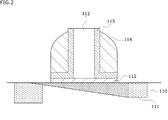
- FIG. 2 is a diagram showing a second example of the main configuration of a semiconductor device to which the technology according to the present disclosure is applied.
- the semiconductor device has a planar structure, and has a laminated structure in which a silicide 111, an insulating film 112, and a gate electrode 113 are laminated as part of the planar structure.
- the silicide 111 is a compound layer formed on the surface of the semiconductor layer 110 such as silicon (Si) and formed by reacting the semiconductor layer 110 with a metal. That is, the silicide 111 is a silicide layer using a metal silicide made of metal and silicon (Si).
- the silicide 111 contains, for example, at least one metal selected from titanium (Ti), cobalt (Co), and nickel (Ni).
- the silicide 111 corresponds to an area represented by a dot pattern (including areas of coarse dots and fine dots), but is formed asymmetrically.
- the left and right square regions represent the silicide formed in the manufacturing process, and are triangular regions in contact with the insulating film 112 (fine dot regions). ) Represents the diffused silicide.
- the insulating film 112 is composed of, for example, an insulating film including a silicon oxide film (SiO 2 ) and a hafnium oxide film (HfO 2 ).
- the gate electrode 113 is composed of, for example, an electrode containing polycrystalline silicon (Poly-Si), tungsten (W), tantalum (Ta), hafnium (Hf), or silicide.
- the sidewall 114 is formed of a silicon nitride film (SiN) or the like as a sidewall of the gate.
- An insulating film 115 such as a silicon oxide film (SiO 2 ) is formed on a portion of the sidewall 114 that is in contact with the gate electrode 113. Note that the sidewall 114 may have a structure in which the insulating film 115 is not formed.
- the semiconductor device shown in FIG. 2 has a planar structure using a silicide 111 based on a CMOS (Complementary Metal Oxide Semiconductor) process
- the silicide 111 formed on the surface of the semiconductor layer 110 is Is formed by forming an electric field effect transistor (FET: Field Effect Transistor) including the silicide 111 on the semiconductor layer 110, and then using electromigration (EM) at the timing of its evaluation or the like.
- FET Field Effect Transistor
- 3A shows a cross-sectional structure of the field effect transistor 151 formed on the semiconductor layer 110.
- silicides 111 are formed on the left and right source and drain portions with respect to the gate electrode 113, respectively.
- electro-migration is performed, for example, in the direction from the drain side to the source side (or from the source side to the drain side). Will be diffused.
- 3B shows a structure of a cross section after the silicide 111 formed in the source and drain portions is diffused by electromigration (EM).
- EM electromigration
- the diffused silicide 111 is formed on the surface of the semiconductor layer 110 as a left-right asymmetric region (a dot pattern region including coarse dots and fine dots) that is in contact with the insulating film 112.
- a laminated structure three-layer structure in which the silicide 111, the insulating film 112, and the gate electrode 113 are laminated is formed.
- Fig. 4 shows an example of a circuit that blows by electromigration (EM).
- EM electromigration
- This blow circuit is driven not at the manufacturing process of the field effect transistors 151-1 to 151-3 but at the timing of its evaluation, and forms a capacitive element (capacitor) to which the present technology is applied by electromigration (EM). is there. Further, the field effect transistors 151-1 to 151-3 have the structure shown in FIG. 3A, and the silicide 111 is formed in each of the source and drain portions.
- the drain is connected to the power supply voltage 161 via the power supply line Vdd, and the source is connected to the power supply line Vss.
- a field effect transistor 162-1 is connected between the drain of the field effect transistor 151-1 and the power supply line Vdd.
- the field effect transistor 162-1 is turned on according to the voltage Vctrl applied to its gate, so that the blow current Ib from the power supply voltage 161 flows from the drain side to the source side of the field effect transistor 151-1. To do so.
- driving the blow circuit causes a positive charge to be applied to the drain of the field effect transistor 151-1. Therefore, the silicide of the channel is supplied from the source side, and the drain is supplied from the source side by electromigration (EM). The silicide 111 is diffused in the side direction.
- EM electromigration
- the field effect transistors 151-2 and 151-3 similarly to the field effect transistor 151-1, the field effect transistors 162-2 and 162-3 are turned on and blown from the power supply voltage 161.
- the silicide 111 is diffused in the direction from the source side to the drain side by electromigration (EM).
- electromigration occurs when metal ions have momentum due to accelerated electrons and move in the semiconductor substrate. That is, in the blow circuit shown in FIG. 4, since the diffusion of the silicide is performed from the negative side to the positive side (electron wind), the channel silicide is supplied from the source side, After the formation, the gate and source terminals can be operated as a capacitive element (capacitor).
- Fig. 5 shows an example of the circuit after blowing by electromigration (EM).
- each of the field effect transistors 162-1 to 162-3 is turned off according to the voltage Vctrl applied to its gate, so that the field effect transistors 151-1 to 151 shown in FIG. -3 and the power supply voltage 161 are separated from each other.
- the capacitor element 152-1 can be operated.
- the silicide 111 is formed immediately below the insulating film 112 of the gate electrode 113, the carrier concentration of the semiconductor substrate can be kept high regardless of the gate voltage, and the voltage dependence can be maintained. The sex can be eased.
- the capacitor elements 152-2 and 152-3 can be operated.
- circuit diagrams of FIGS. 4 and 5 exemplify the case where the field effect transistors 151-1 to 151-3 are formed in the semiconductor device in the manufacturing process, two or less or four or more field effect transistors 151 are formed. When formed, it can be similarly configured.
- the gate and the source and the gate and the drain are short-circuited before and after electromigration (EM). Can be prevented.
- EM electromigration
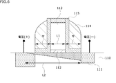
- FIG. 6 shows a structure of a cross section when diffusion of the silicide 111 by electromigration (EM) is appropriate. Further, FIG. 7 shows a top view corresponding to the cross-sectional view shown in FIG.
- EM electromigration
- the EM diffusion length L2 is generally determined by the voltage and the temperature.
- the voltage for example, in the blow circuit (FIG. 4) described above, the voltage (comparison Higher voltage).
- the temperature for example, by setting a higher temperature, the silicide 111 can be diffused further, and the diffusion length L2 can be increased.
- the EM diffusion length L2 can be determined so that the condition of Expression (1) is satisfied at least by the voltage.
- the gate length L1 is shorter than the diffusion length L2.
- the silicide 111 when the voltage is applied from the voltage (+) side to the voltage ( ⁇ ) side, that is, from the source side to the drain side, the silicide 111 is extracted so as to be extracted from the voltage ( ⁇ ) side to the voltage (+) side. Represents the movement of. That is, in this example, the silicide 111 in the voltage ( ⁇ ) side region diffuses (stretches and extends) from the voltage ( ⁇ ) side toward the voltage (+) side, and It reaches the silicide 111.
- the area of the silicide 111 (area of dot pattern including coarse dots and fine dots) includes areas having different densities.
- the material of the silicide 111 for example, metals such as titanium (Ti), cobalt (Co), and nickel (Ni) can be used, as described above. Then, nickel (Ni) is the most diffusive metal, and it is sufficient to apply a voltage that satisfies the condition of the formula (1) in consideration of it.
- the EM diffusion length L2 determined by the voltage and the like has the relationship of Expression (1), and the diffusion of the silicide 111 reaches from the voltage ( ⁇ ) side to the voltage (+) side. Therefore, the gate and drain terminals can operate as a capacitor.
- the voltage (+) side is the source side and the voltage ( ⁇ ) side is the drain side in FIG. 6, the structure is the same regardless of which side the source or the drain is applied. Therefore, the source and the drain may be reversed.
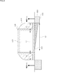
- FIG. 8 shows a cross-sectional structure when the diffusion of the silicide 111 due to electromigration (EM) is short.
- the EM diffusion length L2 determined by the voltage or the like has the relationship of the equation (2), and the diffusion of the silicide 111 from the voltage ( ⁇ ) side region to the voltage (+) side region is performed. Has not reached.
- the silicide 111 is formed on the surface of the semiconductor layer 110, although it is inferior in terms of characteristics and variations as compared with the case of satisfying the relation of the above expression (1).
- the characteristics and the like can be improved.
- a voltage is applied between the drain and the source of a desired gate capacitance, so that the silicide is (selectively) formed by electromigration (EM).
- EM electromigration
- 111 is diffused to form a laminated structure (three-layer structure) in which the silicide 111, the insulating film 112, and the gate electrode 113 are laminated.
- planar structure using the silicide 111 based on the CMOS process is illustrated, but the present technology is not limited to the planar structure and can be applied to other structures. Therefore, next, a case where the present technology is applied to a structure other than the planar structure will be described with reference to FIGS. 9 to 11.
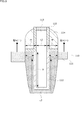
- FIG. 9 shows a trench gate type structure (trench gate structure) in which a trench is formed in the semiconductor layer 110 and the gate electrode 113 is embedded therein.
- the silicide 111 is diffused by electromigration (EM), and the channel is silicided. There is. Accordingly, even in the case of the trench gate structure, a laminated structure (three-layer structure) in which the silicide 111, the insulating film 112, and the gate electrode 113 are laminated is formed.
- EM electromigration
- the EM diffusion length L2 determined by the voltage or the like has the relationship of, for example, the formula (3), and when the diffusion of the silicide 111 reaches between the source and the drain, the capacitive element It is possible to operate as.
- FIGS. 10 and 11 show a three-dimensional structure (fin structure) in which channels are surrounded by gates from multiple directions.
- silicide is formed in the channel region, and the capacitive element (gate capacitive element) having the three-layer structure of the electrode, the oxide film, and the silicide is included.
- the capacitive element since the semiconductor substrate side is silicidized, a capacitance having a characteristic that the capacitance change with respect to the gate voltage can be almost ignored is realized, and the voltage dependence is improved even when the gate capacitance type structure is used. It becomes possible to do.
- Patent Documents 1 and 2 disclose a structure including a silicide layer formed by the reaction of a silicon layer and a metal on the surface of the silicon layer, and a Schottky source/drain structure, There is no disclosure regarding a three-layer structure (electrode, oxide film, silicide) to which the present technique is applied.
- a single slope integration type ADC is often used as an AD conversion circuit (ADC: Analog to Digital Converter).
- ADC Analog to Digital Converter
- the capacitance element used in this AD conversion circuit is generally the MOM type using a wiring layer or the gate capacitance type because of the affinity with the CMOS process, but the MOM type has a large area penalty.
- the gate capacitance type although the area can be saved, there is a problem that the voltage dependency is poor and nonlinear distortion occurs.
- the voltage dependency of the gate capacitance type can be improved to some extent by increasing the substrate impurity concentration to the 20th power or higher, but a deterioration of about 1% remains.
- a high-concentration N-type impurity is introduced and then a high temperature process such as oxidation or a polysilicon gate is processed, variations due to out-diffusion also pose a problem.
- the silicide is diffused by electromigration (EM), and the channel is silicidized.
- EM electromigration
- a capacitor (gate capacitor) having a three-layer structure of a film and a silicide is formed.
- the carrier concentration of the semiconductor substrate can be kept high regardless of the gate voltage, so that the voltage dependence is relaxed. can do.
- the capacitive element excellent in this voltage dependency as a capacitive element used in, for example, an AD conversion circuit, it becomes possible to reduce the non-linear distortion in the ADC, and in a solid-state imaging device such as a CMOS image sensor.
- a solid-state imaging device such as a CMOS image sensor.
- the image quality of a captured image obtained by capturing an image of a subject can be improved.
- the configuration of the solid-state imaging device including the capacitive element having such a three-layer structure will be described.
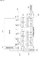
- FIG. 12 shows an example of the configuration of a solid-state imaging device to which the technology according to the present disclosure is applied.
- the solid-state imaging device 200 includes a pixel section 210, a vertical scanning circuit 220, a horizontal transfer scanning circuit 230, a timing control circuit 240, an AD conversion circuit 250, a DAC/bias circuit 260, an amplifier circuit 270, and a signal processing circuit 280.
- a pixel section 210 a vertical scanning circuit 220, a horizontal transfer scanning circuit 230, a timing control circuit 240, an AD conversion circuit 250, a DAC/bias circuit 260, an amplifier circuit 270, and a signal processing circuit 280.
- the pixel portion 210 is configured by arranging pixels including a photodiode (PD: Photodiode) and pixel transistors in a two-dimensional (matrix) shape.
- PD photodiode
- pixel transistors in a two-dimensional (matrix) shape. The detailed configuration of the pixels arranged in the pixel portion 210 will be described later with reference to FIG.
- a timing control circuit 240 that generates an internal clock and a vertical scanning circuit 220 that controls a row address and a row scanning are provided as a control circuit for sequentially reading out signals of (the pixels arranged in) the pixel section 210.
- a horizontal transfer scanning circuit 230 for controlling column addresses and column scanning is provided.
- the timing control circuit 240 generates and supplies necessary timing signals to the pixel section 210, vertical scanning circuit 220, horizontal transfer scanning circuit 230, AD conversion circuit 250, DAC/bias circuit 260, and signal processing circuit 280.
- the pixel section 210 for example, photons are accumulated and discharged using a line shutter to photoelectrically convert the image image for each pixel row, and the resulting analog signal is output to the AD conversion circuit 250 via the vertical signal line VSL. ..
- the ramp signal (RAMP) from the DAC (Digital to Analog Converter) 261 included in the DAC/bias circuit 260 is used for the analog signal from the pixel unit 210 in each ADC block (each column unit). Integral type ADC and Correlated Double Sampling (CDS) are performed and the digital signal (of several bits) is output.
- RAMP ramp signal
- CDS Correlated Double Sampling
- a comparator 251 that compares the ramp signal generated by the DAC 261 with an analog signal (potential VSL) obtained from the pixel via the vertical signal line VSL for each row line, and a comparison time.
- a plurality of ADCs each including a counter 252 that counts the count and a latch 253 that holds the count result are arrayed.
- the ramp signal is a reference voltage Vslop that is a ramp waveform (RAMP) obtained by stepwise changing the reference voltage generated by the DAC 261.
- the AD conversion circuit 250 has an n-bit digital conversion function and is arranged for each vertical signal line VSL to form a column parallel ADC block.
- the output of each latch 253 is connected to, for example, a horizontal transfer line LTFR having a 2n-bit width. Further, 2n amplifier circuits 270 and a signal processing circuit 280 corresponding to the horizontal transfer line LTFR are arranged.
- the detailed configuration of the comparator 251 included in the AD conversion circuit 250 will be described later with reference to FIG.
- the analog signal (potential VSL) read to the vertical signal line VSL is changed by the reference voltage Vslop (linear change with a certain slope) by the comparator 251 arranged for each column (each column).
- Ramp signal which is a slope waveform that At this time, the counters 252 arranged in columns are operating similarly to the comparator 251, and the ramp signal (potential Vslop) having a ramp waveform and the counter value change in a one-to-one correspondence to change the vertical direction.
- the analog signal (potential VSL) of the signal line VSL is converted into a digital signal.
- the change in the reference voltage Vslop is to convert the change in voltage into a change in time, and the time is counted in a certain cycle (clock) to be converted into a digital value. Then, when the analog signal (potential VSL) and the ramp signal (reference voltage Vslop) intersect, the output of the comparator 251 is inverted and the input clock of the counter 252 is stopped, or the clock whose input is stopped is counted. Input to 252 to complete AD conversion.
- the signal held in the latch 253 is transferred to the horizontal transfer line LTFR by the horizontal transfer scanning circuit 230 and input to the signal processing circuit 280 via the amplifier circuit 270.
- the signal processing circuit 280 predetermined signal processing (for example, correction of vertical line defect or point defect) is performed on the signal input thereto, and the image signal obtained by the signal processing is output to the subsequent stage. ..
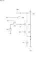
- FIG. 13 shows an example of a detailed configuration of the pixels 211 arranged two-dimensionally in the pixel section 210 of FIG.
- the pixel 211 has a photodiode 212 as a photoelectric conversion element, and has four pixel transistors of a transfer transistor 213, an amplification transistor 214, a selection transistor 215, and a reset transistor 216 for the photodiode 212.
- the photodiode 212 photoelectrically converts incident light into electric charge according to the amount of light.
- the transfer transistor 213 is connected between the photodiode 212 and the floating diffusion FD, and when a transfer control signal (TG) is applied to its gate, the transfer transistor 213 transfers the charge photoelectrically converted by the photodiode 212 to the floating diffusion FD. ..
- the gate of the amplification transistor 214 is connected to the floating diffusion FD.
- the amplification transistor 214 is connected to the vertical signal line VSL via the selection transistor 215, and constitutes a constant current source 217 outside the pixel section 210 and a source follower.
- the amplification transistor 214 amplifies the potential of the floating diffusion FD and outputs a voltage corresponding to the potential. Output to the vertical signal line VSL.
- the signal voltage (analog signal) output from the pixel 211 is input to the AD conversion circuit 250 via the vertical signal line VSL.
- the reset transistor 216 is connected between the power supply line Vdd and the floating diffusion FD, and when a reset control signal (RST) is applied to its gate, resets the potential of the floating diffusion FD to the potential of the power supply line Vdd.
- RST reset control signal
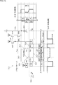
- FIG. 14 shows an example of a detailed configuration of the comparator 251 included in the AD conversion circuit 250 of FIG.
- a first amplifier 251A having a function of performing a low-speed signal comparison operation in the first stage to narrow the operation band and a second amplifier 251B having a function of increasing the output of the first amplifier 251A are provided. Cascaded.
- the comparator 251 outputs the first AZ (initialization) signal PSEL for the first amplifier 251A, which is applied to the AZ switch for determining the operating point to each column at the start of the row operation, in the horizontal direction (of the comparator).
- the AZ switch of the non-operation comparator is fixed to OFF at the start of the non-operation row by independently controlling the intermittent operation basic units in the array direction and the column direction) in parallel.
- the first amplifier 251A has PMOS transistors 291A to 291E, NMOS transistors 292A to 292D, and capacitors 293A and 293B that are AZ level sampling capacitors.
- the PMOS transistors 291A and 291B configure a current mirror circuit
- the NMOS transistors 292A and 292B configure a differential comparison unit using the NMOS transistor 292C as a current source.
- the PMOS transistors 291C and 291D function as AZ switches
- the capacitors 293A and 293B function as AZ level sampling capacitors.
- capacitors 293A and 293B capacitors to which the present technology is applied, that is, capacitors having a three-layer structure of an electrode, an oxide film, and a silicide can be used.
- the second amplifier 251B has a PMOS transistor 294A, NMOS transistors 295A and 295B, and a capacitor 296A which is an AZ level sampling capacitance.
- the PMOS transistor 294A constitutes an input and current source circuit.
- the NMOS transistor 295B functions as an AZ switch
- the capacitor 296A functions as an AZ level sampling capacity.
- the capacitor 296A a capacitor to which the present technique is applied, that is, a capacitor having a three-layer structure of an electrode, an oxide film, and a silicide can be used.
- the capacitors 293A, 293B, and 296A provided in (the comparator 251 of) the AD conversion circuit 250 As described above, in the solid-state imaging device 200, as the capacitors 293A, 293B, and 296A provided in (the comparator 251 of) the AD conversion circuit 250, a capacitive element having a three-layer structure (electrode, oxide film, silicide) to which the present technology is applied. By using (capacitance element with improved gate capacitance type voltage dependency), nonlinear distortion in the ADC can be reduced, and as a result, the quality of the captured image can be improved.
- FIG. 15 shows an example of a detailed configuration of the pixel 311 as another configuration of the pixels arranged two-dimensionally in the pixel portion 210 of FIG.
- the pixel 311 has a photodiode 312, and for this photodiode 312, a first transfer transistor 313, a second transfer gate unit 314, a third transfer gate unit 315, a reset transistor 316, and a first charge storage A portion 317, a second charge storage portion 318, an amplification transistor 319, a selection transistor 320, and a charge discharge transistor 321 are included.
- a first charge storage section 317 and a second charge storage section 318 are provided as areas for storage.
- an embedded MOS capacitor can be used as the first charge storage unit 317, and a MOS capacitor having a larger capacitance value per unit area than the first charge storage unit 317 can be used as the second charge storage unit 318.
- the photodiode 312 photoelectrically converts incident light into electric charges according to the amount of light.
- the first transfer transistor 313 is connected between the photodiode 312 and the first charge storage unit 317, and when a transfer control signal (TG) is applied to the gate of the first transfer transistor 313, the first photoelectrically converted charge of the photodiode 312 is transferred to the first transfer transistor 313.
- the charge is transferred to the 1-charge storage unit 317.
- the first charge storage unit 317 temporarily stores the charges transferred from the first transfer transistor 313.
- the second transfer gate unit 314 is connected to the first charge storage unit 317 and the floating diffusion FD.
- the transfer control signal (FG) is applied to the gate of the second transfer gate unit 314, the charge stored in the first charge storage unit 317 is floated. Transfer to the diffusion FD.
- the third transfer gate unit 315 is connected between the first charge storage unit 317 and the second charge storage unit 318, and when the transfer control signal (CG) is applied to its gate, the third transfer gate unit 317 and the first charge storage unit 317 are connected to each other. The potentials of the two charge storage units 318 are combined.
- the reset transistor 316 is connected between the power supply line Vdr and the floating diffusion FD, and when a reset control signal (RST) is given to its gate, the potential of the floating diffusion FD is reset to the potential of the power supply line Vdr.
- RST reset control signal
- the gate of the amplification transistor 319 is connected to the floating diffusion FD.
- the amplification transistor 319 is connected to the vertical signal line VSL via the selection transistor 320, and constitutes a constant current source 322 outside the pixel portion 210 (FIG. 12) and a source follower.
- the amplification transistor 319 amplifies the potential of the floating diffusion FD and outputs a voltage corresponding to the potential.
- the signal is output to the AD conversion circuit 250 (FIG. 12) via the vertical signal line VSL.
- charge discharging transistor 321 is connected between the photodiode 312 and the power supply line Vdd (charge discharging unit), and when the charge discharging control signal (PG) is given to its gate, the charge stored in the photodiode 312 is charged. Is selectively discharged.
- FIG. 16 is a schematic diagram showing the configuration of the pixel 311, and the same reference numerals are given to the portions corresponding to FIG. Note that FIG. 16 shows a plane pattern showing a pixel layout, a sectional view taken along the line AA′ of the plane pattern, and a sectional view taken along the line BB′ of the plane pattern.
- a capacitor to which the present technology is applied is used as a capacitor forming the second charge storage unit 318, that is, a capacitor having a three-layer structure of an electrode, an oxide film, and a silicide (gate capacitance It is possible to use a capacitive element having improved mold voltage dependency.
- the pixel section 210 and the peripheral circuit section including the AD conversion circuit 250 and the like may be formed on the same substrate or may be formed on different substrates. That is, in the solid-state imaging device 200 (for example, a back-illuminated CMOS image sensor), for example, the pixel portion 210 is formed in the first semiconductor layer and the second semiconductor is formed by using a structure in which a plurality of semiconductor layers are stacked. A structure in which a peripheral circuit portion including the AD conversion circuit 250 and the like is formed in a layer can be used.
- the solid-state imaging device 200 (FIG. 12) described above is, for example, various electronic devices such as an imaging device such as a digital still camera or a digital video camera, a mobile phone or a smartphone having an imaging function, or another device having an imaging function. Can be applied to.
- an imaging device such as a digital still camera or a digital video camera
- a mobile phone or a smartphone having an imaging function or another device having an imaging function. Can be applied to.
- FIG. 17 is a block diagram showing an example of the configuration of an electronic device equipped with a solid-state imaging device to which the technology according to the present disclosure is applied.
- an electronic device 1000 includes an optical system 1001, a shutter device 1002, a solid-state imaging device 1003, a control circuit 1004, a signal processing circuit 1005, a monitor 1006, and a memory 1007, and captures a still image or a moving image. It is possible.
- the optical system 1001 is configured to have one or a plurality of lenses, guides light (incident light) from a subject to the solid-state imaging device 1003, and forms an image on the light-receiving surface of the solid-state imaging device 1003.
- the shutter device 1002 is arranged between the optical system 1001 and the solid-state imaging device 1003, and controls the light irradiation period and the shielding period to the solid-state imaging device 1003 under the control of the control circuit 1004.
- the solid-state imaging device 1003 is configured, for example, as a package including the above-described solid-state imaging device 200 (FIG. 12). Under the control of the control circuit 1004, the solid-state imaging device 1003 accumulates a charge corresponding to the light imaged on the light receiving surface via the optical system 1001 and the shutter device 1002 and reads it out at a predetermined timing to perform AD conversion or predetermined conversion. An image signal is generated by performing the signal processing of (1) and is supplied to the signal processing circuit 1005.
- the control circuit 1004 generates a drive signal that controls the shutter operation of the shutter device 1002 and the transfer operation of the solid-state imaging device 1003, and drives the shutter device 1002 and the solid-state imaging device 1003.
- the signal processing circuit 1005 is configured as, for example, a camera ISP (Image Signal Processor) or the like.
- the signal processing circuit 1005 uses the image signal output from the solid-state imaging device 1003 to perform various kinds of signal processing such as demosaicing, color space conversion, resolution conversion, and codec.
- the signal processing circuit 1005 supplies the image data (of the captured image) obtained by the signal processing to the monitor 1006 or the memory 1007.
- the monitor 1006 is composed of a display device such as a liquid crystal display or an OLED (Organic Light Emitting Diode) display.
- the monitor 1006 displays an image corresponding to the image data supplied from the signal processing circuit 1005.
- the memory 1007 is composed of a storage device such as a semiconductor memory.
- the memory 1007 stores the image data supplied from the signal processing circuit 1005.
- the AD conversion circuit 250 (comparator 251 thereof) and the global shutter are supported.
- a capacitor provided in (the pixel 311 of) the formed pixel portion 210 a capacitive element having a three-layer structure (electrode, oxide film, silicide) to which the present technology is applied (capacitive element with improved gate capacitance type voltage dependency) is used. To be Therefore, the non-linear distortion in the ADC can be reduced, and as a result, the image quality of the captured image can be improved.
- the technology according to the present disclosure (this technology) can be applied to various products.
- the technology according to the present disclosure may be applied to an endoscopic surgery system.
- FIG. 18 is a diagram showing an example of a schematic configuration of an endoscopic surgery system to which the technology according to the present disclosure (the present technology) can be applied.
- FIG. 18 illustrates a situation in which an operator (doctor) 11131 is operating on a patient 11132 on a patient bed 11133 using the endoscopic surgery system 11000.
- the endoscopic surgery system 11000 includes an endoscope 11100, other surgical tools 11110 such as a pneumoperitoneum tube 11111 and an energy treatment tool 11112, and a support arm device 11120 that supports the endoscope 11100.
- a cart 11200 on which various devices for endoscopic surgery are mounted.
- the endoscope 11100 is composed of a lens barrel 11101 into which a region having a predetermined length from the distal end is inserted into the body cavity of the patient 11132, and a camera head 11102 connected to the base end of the lens barrel 11101.
- the endoscope 11100 configured as a so-called rigid mirror having the rigid barrel 11101 is illustrated, but the endoscope 11100 may be configured as a so-called flexible mirror having a flexible barrel. Good.
- An opening in which an objective lens is fitted is provided at the tip of the lens barrel 11101.
- a light source device 11203 is connected to the endoscope 11100, and light generated by the light source device 11203 is guided to the tip of the lens barrel by a light guide extending inside the lens barrel 11101. It is irradiated toward the observation target in the body cavity of the patient 11132 via the lens.
- the endoscope 11100 may be a direct-viewing endoscope, or may be a perspective or side-viewing endoscope.
- An optical system and an image pickup device are provided inside the camera head 11102, and the reflected light (observation light) from the observation target is condensed on the image pickup device by the optical system.
- the observation light is photoelectrically converted by the imaging element, and an electric signal corresponding to the observation light, that is, an image signal corresponding to the observation image is generated.
- the image signal is transmitted as RAW data to a camera control unit (CCU: Camera Control Unit) 11201.
- CCU Camera Control Unit
- the CCU 11201 is configured by a CPU (Central Processing Unit), a GPU (Graphics Processing Unit), and the like, and integrally controls the operations of the endoscope 11100 and the display device 11202. Further, the CCU 11201 receives the image signal from the camera head 11102, and performs various image processing such as development processing (demosaic processing) on the image signal for displaying an image based on the image signal.
- image processing such as development processing (demosaic processing)
- the display device 11202 displays an image based on an image signal subjected to image processing by the CCU 11201 under the control of the CCU 11201.
- the light source device 11203 is configured by a light source such as an LED (Light Emitting Diode), and supplies the endoscope 11100 with irradiation light when imaging a surgical site or the like.
- a light source such as an LED (Light Emitting Diode)
- LED Light Emitting Diode
- the input device 11204 is an input interface for the endoscopic surgery system 11000.
- the user can input various kinds of information and instructions to the endoscopic surgery system 11000 via the input device 11204.
- the user inputs an instruction to change the imaging conditions (type of irradiation light, magnification, focal length, etc.) by the endoscope 11100.
- the treatment instrument control device 11205 controls driving of the energy treatment instrument 11112 for cauterization of tissue, incision, sealing of blood vessel, or the like.
- the pneumoperitoneum device 11206 is used to inflate the body cavity of the patient 11132 through the pneumoperitoneum tube 11111 in order to inflate the body cavity of the patient 11132 for the purpose of securing the visual field by the endoscope 11100 and the working space of the operator.
- the recorder 11207 is a device capable of recording various information regarding surgery.
- the printer 11208 is a device that can print various types of information regarding surgery in various formats such as text, images, or graphs.
- the light source device 11203 that supplies the endoscope 11100 with irradiation light when imaging a surgical site can be configured by, for example, an LED, a laser light source, or a white light source configured by a combination thereof.
- a white light source is formed by a combination of RGB laser light sources
- the output intensity and output timing of each color (each wavelength) can be controlled with high accuracy, so that the light source device 11203 adjusts the white balance of the captured image. It can be carried out.
- the laser light from each of the RGB laser light sources is time-divisionally irradiated to the observation target, and the drive of the image pickup device of the camera head 11102 is controlled in synchronization with the irradiation timing to correspond to each of RGB. It is also possible to take the captured image in a time division manner. According to this method, a color image can be obtained without providing a color filter on the image sensor.
- the drive of the light source device 11203 may be controlled so as to change the intensity of the output light at predetermined time intervals.
- the drive of the image sensor of the camera head 11102 in synchronism with the timing of changing the intensity of the light to acquire an image in a time-division manner and synthesizing the images, a high dynamic image without so-called blackout and overexposure Images of the range can be generated.
- the light source device 11203 may be configured to be able to supply light in a predetermined wavelength band corresponding to special light observation.
- special light observation for example, by utilizing the wavelength dependence of absorption of light in body tissues, by irradiating a narrow band of light as compared with irradiation light (that is, white light) in normal observation, the mucosal surface layer
- the so-called narrow band imaging is performed in which a predetermined tissue such as a blood vessel is imaged with high contrast.
- fluorescence observation in which an image is obtained by the fluorescence generated by irradiating the excitation light may be performed.
- the body tissue is irradiated with excitation light to observe the fluorescence from the body tissue (autofluorescence observation), or a reagent such as indocyanine green (ICG) is locally injected into the body tissue and the body tissue is injected.
- the excitation light corresponding to the fluorescence wavelength of the reagent can be irradiated to obtain a fluorescence image or the like.
- the light source device 11203 may be configured to be able to supply the narrow band light and/or the excitation light corresponding to such special light observation.
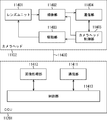
- FIG. 19 is a block diagram showing an example of the functional configuration of the camera head 11102 and the CCU 11201 shown in FIG.
- the camera head 11102 includes a lens unit 11401, an imaging unit 11402, a driving unit 11403, a communication unit 11404, and a camera head control unit 11405.
- the CCU 11201 has a communication unit 11411, an image processing unit 11412, and a control unit 11413.
- the camera head 11102 and the CCU 11201 are communicably connected to each other via a transmission cable 11400.
- the lens unit 11401 is an optical system provided at the connecting portion with the lens barrel 11101.
- the observation light taken in from the tip of the lens barrel 11101 is guided to the camera head 11102 and enters the lens unit 11401.
- the lens unit 11401 is configured by combining a plurality of lenses including a zoom lens and a focus lens.
- the image pickup unit 11402 includes an image pickup element.
- the number of image pickup elements forming the image pickup unit 11402 may be one (so-called single-plate type) or plural (so-called multi-plate type).
- image signals corresponding to R, G, and B may be generated by the respective image pickup elements, and these may be combined to obtain a color image.
- the image capturing unit 11402 may be configured to have a pair of image capturing elements for respectively acquiring image signals for the right eye and the left eye corresponding to 3D (Dimensional) display.
- the 3D display enables the operator 11131 to more accurately grasp the depth of the living tissue in the operation site.
- a plurality of lens units 11401 may be provided corresponding to each image pickup element.
- the image pickup unit 11402 does not necessarily have to be provided in the camera head 11102.
- the imaging unit 11402 may be provided inside the lens barrel 11101 immediately after the objective lens.
- the drive unit 11403 is composed of an actuator, and moves the zoom lens and the focus lens of the lens unit 11401 by a predetermined distance along the optical axis under the control of the camera head control unit 11405. Accordingly, the magnification and focus of the image captured by the image capturing unit 11402 can be adjusted as appropriate.
- the communication unit 11404 is composed of a communication device for transmitting/receiving various information to/from the CCU 11201.
- the communication unit 11404 transmits the image signal obtained from the imaging unit 11402 as RAW data to the CCU 11201 via the transmission cable 11400.
- the communication unit 11404 receives a control signal for controlling the driving of the camera head 11102 from the CCU 11201, and supplies it to the camera head control unit 11405.
- the control signal includes, for example, information that specifies the frame rate of the captured image, information that specifies the exposure value at the time of capturing, and/or information that specifies the magnification and focus of the captured image. Contains information about the condition.
- the image capturing conditions such as the frame rate, the exposure value, the magnification, and the focus may be appropriately designated by the user, or may be automatically set by the control unit 11413 of the CCU 11201 based on the acquired image signal. Good. In the latter case, the so-called AE (Auto Exposure) function, AF (Auto Focus) function, and AWB (Auto White Balance) function are installed in the endoscope 11100.
- AE Auto Exposure
- AF Auto Focus
- AWB Auto White Balance
- the camera head control unit 11405 controls the driving of the camera head 11102 based on the control signal from the CCU 11201 received via the communication unit 11404.
- the communication unit 11411 is composed of a communication device for transmitting and receiving various information to and from the camera head 11102.
- the communication unit 11411 receives the image signal transmitted from the camera head 11102 via the transmission cable 11400.
- the communication unit 11411 transmits a control signal for controlling the driving of the camera head 11102 to the camera head 11102.
- the image signal and the control signal can be transmitted by electric communication, optical communication, or the like.
- the image processing unit 11412 performs various types of image processing on the image signal that is the RAW data transmitted from the camera head 11102.
- the control unit 11413 performs various controls regarding imaging of a surgical site or the like by the endoscope 11100 and display of a captured image obtained by imaging the surgical site or the like. For example, the control unit 11413 generates a control signal for controlling the driving of the camera head 11102.
- the control unit 11413 also causes the display device 11202 to display a captured image of the surgical site or the like based on the image signal subjected to the image processing by the image processing unit 11412. At this time, the control unit 11413 may recognize various objects in the captured image using various image recognition techniques. For example, the control unit 11413 detects a surgical instrument such as forceps, a specific body part, bleeding, and a mist when the energy treatment instrument 11112 is used by detecting the shape and color of the edge of the object included in the captured image. Can be recognized. When displaying the captured image on the display device 11202, the control unit 11413 may use the recognition result to superimpose and display various types of surgery support information on the image of the operation unit. By displaying the surgery support information in a superimposed manner and presenting it to the operator 11131, the burden on the operator 11131 can be reduced, and the operator 11131 can reliably proceed with the surgery.
- a surgical instrument such as forceps, a specific body part, bleeding, and a mist when
- the transmission cable 11400 that connects the camera head 11102 and the CCU 11201 is an electric signal cable compatible with electric signal communication, an optical fiber compatible with optical communication, or a composite cable of these.
- wired communication is performed using the transmission cable 11400, but communication between the camera head 11102 and the CCU 11201 may be performed wirelessly.
- the example of the endoscopic surgery system to which the technology according to the present disclosure can be applied has been described above.
- the technology according to the present disclosure may be applied to the endoscope 11100 and (the imaging unit 11402 of) the camera head 11102 among the configurations described above.
- the solid-state imaging device 200 of FIG. 12 can be applied to, for example, the imaging unit 11402.
- the technique according to the present disclosure to the imaging unit 11402, for example, it is possible to reduce the nonlinear distortion in the ADC and obtain a clearer surgical region image, so that the surgeon can more reliably detect the surgical region. It becomes possible to confirm.
- the technology according to the present disclosure (this technology) can be applied to various products.
- the technology according to the present disclosure is realized as a device mounted on any type of moving body such as an automobile, an electric vehicle, a hybrid electric vehicle, a motorcycle, a bicycle, personal mobility, an airplane, a drone, a ship, and a robot. May be.
- FIG. 20 is a block diagram showing a schematic configuration example of a vehicle control system that is an example of a mobile body control system to which the technology according to the present disclosure can be applied.
- the vehicle control system 12000 includes a plurality of electronic control units connected via a communication network 12001.
- the vehicle control system 12000 includes a drive system control unit 12010, a body system control unit 12020, a vehicle exterior information detection unit 12030, a vehicle interior information detection unit 12040, and an integrated control unit 12050.
- a microcomputer 12051 As a functional configuration of the integrated control unit 12050, a microcomputer 12051, a voice image output unit 12052, and an in-vehicle network I/F (Interface) 12053 are shown.
- the drive system control unit 12010 controls the operation of devices related to the drive system of the vehicle according to various programs.
- the drive system control unit 12010 includes a drive force generation device for generating a drive force of a vehicle such as an internal combustion engine or a drive motor, a drive force transmission mechanism for transmitting the drive force to wheels, and a steering angle of the vehicle. It functions as a steering mechanism for adjustment and a control device such as a braking device that generates a braking force of the vehicle.
- the body system control unit 12020 controls the operation of various devices mounted on the vehicle body according to various programs.
- the body system control unit 12020 functions as a keyless entry system, a smart key system, a power window device, or a control device for various lamps such as a head lamp, a back lamp, a brake lamp, a winker, or a fog lamp.
- the body system control unit 12020 may receive radio waves or signals of various switches transmitted from a portable device that substitutes for a key.
- the body system control unit 12020 receives input of these radio waves or signals and controls the vehicle door lock device, power window device, lamp, and the like.
- the vehicle exterior information detection unit 12030 detects information outside the vehicle equipped with the vehicle control system 12000.
- the imaging unit 12031 is connected to the vehicle outside information detection unit 12030.
- the vehicle exterior information detection unit 12030 causes the image capturing unit 12031 to capture an image of the vehicle exterior and receives the captured image.
- the vehicle exterior information detection unit 12030 may perform object detection processing or distance detection processing such as people, vehicles, obstacles, signs, or characters on the road surface based on the received image.
- the image pickup unit 12031 is an optical sensor that receives light and outputs an electric signal according to the amount of received light.
- the imaging unit 12031 can output the electric signal as an image or as distance measurement information.
- the light received by the imaging unit 12031 may be visible light or invisible light such as infrared light.
- the in-vehicle information detection unit 12040 detects in-vehicle information.
- a driver state detection unit 12041 that detects the state of the driver is connected.
- the driver state detection unit 12041 includes, for example, a camera that images the driver, and the in-vehicle information detection unit 12040 determines the degree of fatigue or concentration of the driver based on the detection information input from the driver state detection unit 12041. It may be calculated or it may be determined whether the driver is asleep.
- the microcomputer 12051 calculates a control target value of the driving force generation device, the steering mechanism, or the braking device based on the information inside or outside the vehicle acquired by the outside information detection unit 12030 or the inside information detection unit 12040, and the drive system control unit.
- a control command can be output to 12010.
- the microcomputer 12051 realizes functions of ADAS (Advanced Driver Assistance System) including collision avoidance or shock mitigation of a vehicle, follow-up traveling based on an inter-vehicle distance, vehicle speed maintenance traveling, a vehicle collision warning, or a vehicle lane departure warning. It is possible to perform cooperative control for the purpose.
- ADAS Advanced Driver Assistance System
- the microcomputer 12051 controls the driving force generation device, the steering mechanism, the braking device, or the like based on the information around the vehicle acquired by the vehicle exterior information detection unit 12030 or the vehicle interior information detection unit 12040, so that the driver's It is possible to perform cooperative control for the purpose of autonomous driving or the like that autonomously travels without depending on the operation.
- the microcomputer 12051 can output a control command to the body system control unit 12020 based on the information outside the vehicle acquired by the outside information detection unit 12030.
- the microcomputer 12051 controls the headlamp according to the position of the preceding vehicle or the oncoming vehicle detected by the vehicle exterior information detection unit 12030, and performs cooperative control for the purpose of antiglare such as switching the high beam to the low beam. It can be carried out.
- the voice image output unit 12052 transmits an output signal of at least one of a voice and an image to an output device capable of visually or audibly notifying information to an occupant of the vehicle or the outside of the vehicle.
- an audio speaker 12061, a display unit 12062, and an instrument panel 12063 are illustrated as output devices.
- the display unit 12062 may include, for example, at least one of an onboard display and a head-up display.
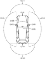
- FIG. 21 is a diagram showing an example of the installation position of the imaging unit 12031.
- the imaging unit 12031 includes imaging units 12101, 12102, 12103, 12104, and 12105.
- the image capturing units 12101, 12102, 12103, 12104, and 12105 are provided, for example, at positions such as the front nose of the vehicle 12100, the side mirrors, the rear bumper, the back door, and the upper portion of the windshield inside the vehicle.
- the image capturing unit 12101 provided on the front nose and the image capturing unit 12105 provided on the upper part of the windshield in the vehicle interior mainly acquire images in front of the vehicle 12100.
- the image capturing units 12102 and 12103 provided in the side mirrors mainly acquire images of the side of the vehicle 12100.
- the imaging unit 12104 provided on the rear bumper or the back door mainly acquires an image of the rear of the vehicle 12100.
- the imaging unit 12105 provided on the upper part of the windshield in the vehicle interior is mainly used for detecting a preceding vehicle, a pedestrian, an obstacle, a traffic signal, a traffic sign, a lane, or the like.
- FIG. 21 shows an example of the shooting range of the imaging units 12101 to 12104.
- the imaging range 12111 indicates the imaging range of the imaging unit 12101 provided on the front nose
- the imaging ranges 12112 and 12113 indicate the imaging ranges of the imaging units 12102 and 12103 provided on the side mirrors
- the imaging range 12114 indicates The imaging range of the imaging part 12104 provided in a rear bumper or a back door is shown.
- a bird's-eye view image of the vehicle 12100 viewed from above can be obtained.
- At least one of the image capturing units 12101 to 12104 may have a function of acquiring distance information.
- at least one of the image capturing units 12101 to 12104 may be a stereo camera including a plurality of image capturing elements, or may be an image capturing element having pixels for phase difference detection.
- the microcomputer 12051 based on the distance information obtained from the image capturing units 12101 to 12104, the distance to each three-dimensional object in the image capturing ranges 12111 to 12114 and the temporal change of this distance (relative speed with respect to the vehicle 12100).
- the closest three-dimensional object on the traveling path of the vehicle 12100 which is traveling at a predetermined speed (for example, 0 km/h or more) in the substantially same direction as the vehicle 12100, can be extracted as a preceding vehicle. it can.
- the microcomputer 12051 can set an inter-vehicle distance to be secured in front of the preceding vehicle, and can perform automatic brake control (including follow-up stop control), automatic acceleration control (including follow-up start control), and the like. In this way, it is possible to perform cooperative control for the purpose of autonomous driving or the like that autonomously travels without depending on the operation of the driver.
- the microcomputer 12051 uses the distance information obtained from the imaging units 12101 to 12104 to convert three-dimensional object data regarding a three-dimensional object into another three-dimensional object such as a two-wheeled vehicle, an ordinary vehicle, a large vehicle, a pedestrian, and a utility pole. It can be classified and extracted and used for automatic avoidance of obstacles. For example, the microcomputer 12051 distinguishes obstacles around the vehicle 12100 into obstacles visible to the driver of the vehicle 12100 and obstacles difficult to see. Then, the microcomputer 12051 determines the collision risk indicating the risk of collision with each obstacle, and when the collision risk is equal to or more than the set value and there is a possibility of collision, the microcomputer 12051 outputs the audio through the audio speaker 12061 and the display unit 12062. A driver can be assisted for collision avoidance by outputting an alarm to the driver and by performing forced deceleration or avoidance steering through the drive system control unit 12010.
- At least one of the imaging units 12101 to 12104 may be an infrared camera that detects infrared rays.
- the microcomputer 12051 can recognize a pedestrian by determining whether or not a pedestrian is present in the images captured by the imaging units 12101 to 12104.
- a procedure of extracting a feature point in an image captured by the image capturing units 12101 to 12104 as an infrared camera and a pattern matching process on a series of feature points indicating the contour of an object are performed to determine whether the pedestrian is a pedestrian. Is performed by the procedure for determining.
- the audio image output unit 12052 causes the recognized pedestrian to have a rectangular contour line for emphasis.
- the display unit 12062 is controlled so as to superimpose and display. Further, the audio image output unit 12052 may control the display unit 12062 so as to display an icon indicating a pedestrian or the like at a desired position.
- the technology according to the present disclosure can be applied to (the image capturing unit 12101 and the like of) the image capturing unit 12031 among the configurations described above.
- the solid-state imaging device 200 of FIG. 12 can be applied to, for example, the imaging unit 12031.
- linear distortion in the ADC can be reduced and a clearer captured image can be obtained. Therefore, for example, more accurately, people, vehicles, and obstacles can be obtained. It is possible to recognize an object such as a sign or a character on the road surface.
- the technology according to the present disclosure can have the following configurations.
- the insulating film layer includes a silicon oxide film (SiO 2 ), The semiconductor device according to (1), wherein the compound layer includes a silicide layer using metal silicide.
- the silicide layer contains at least one metal selected from titanium (Ti), cobalt (Co), and nickel (Ni).
- the silicide layer includes regions having different concentrations.
- the electrode layer is configured as a gate electrode, The semiconductor device according to (4), wherein the silicide layer has a different concentration in the left and right regions with respect to the gate electrode.
- the electrode layer is configured as a gate electrode, The semiconductor device according to any one of (1) to (5), wherein the stacked structure is configured as a part of a structure corresponding to a field effect transistor.
- the semiconductor device according to (6), wherein the structure includes a planar structure, a trench gate structure, or a fin structure.
- the semiconductor layer includes at least a first semiconductor layer and a second semiconductor layer, A plurality of the pixels are formed on the first semiconductor layer, The solid-state imaging device according to (8) or (9), wherein the AD conversion unit is formed on the second semiconductor layer.
- An electrode layer is formed on the insulating film layer, A method of manufacturing a semiconductor device, comprising: forming a compound layer formed on a surface of a semiconductor layer so as to contact the insulating film layer, the compound layer being formed by a reaction between the semiconductor layer and a metal.
- the electrode layer is used as a gate electrode, and a field effect transistor containing silicide is formed in the semiconductor layer, The method for manufacturing a semiconductor device according to (11), wherein the silicide is diffused by electromigration to form the compound layer.
- the insulating film layer includes a silicon oxide film (SiO 2 ), The method for manufacturing a semiconductor device according to (12), wherein the silicide contains at least one metal selected from titanium (Ti), cobalt (Co), and nickel (Ni).
- the method of manufacturing a semiconductor device according to (14), wherein the silicide has a different concentration in right and left regions with respect to the gate electrode.
Landscapes
- Engineering & Computer Science (AREA)
- Multimedia (AREA)
- Signal Processing (AREA)
- Metal-Oxide And Bipolar Metal-Oxide Semiconductor Integrated Circuits (AREA)
- Insulated Gate Type Field-Effect Transistor (AREA)
- Solid State Image Pick-Up Elements (AREA)
- Transforming Light Signals Into Electric Signals (AREA)
- Internal Circuitry In Semiconductor Integrated Circuit Devices (AREA)
- Semiconductor Integrated Circuits (AREA)
Abstract
本開示は、ゲート容量型の電圧依存性を改善することができるようにする半導体装置、固体撮像装置、及び半導体装置の製造方法に関する。 半導体層の表面に形成され、半導体層と金属とが反応して形成された化合物層と、化合物層と接する絶縁膜層と、絶縁膜層の上に形成される電極層とが積層された積層構造を有する半導体装置が提供される。本技術は、例えば、固体撮像装置に含まれるAD変換部に適用することができる。
Description
本開示は、半導体装置、固体撮像装置、及び半導体装置の製造方法に関し、特に、ゲート容量型の電圧依存性を改善することができるようにした半導体装置、固体撮像装置、及び半導体装置の製造方法に関する。
例えば、容量素子として、MOM(Metal-Oxide-Metal)型やMIM(Metal-Insulator-Metal)型、ゲート容量型などの素子が知られている。
特許文献1には、シリコン層の表面に、シリコン層と金属とが反応して形成されたシリサイド層を含む構造が開示されている。また、特許文献2には、ショットキーソース・ドレイン構造について開示されている。
ところで、ゲート容量型の素子は、他の容量素子と比べて電圧依存性が劣るため、電圧依存性を改善することが求められている。
本開示はこのような状況に鑑みてなされたものであり、ゲート容量型の電圧依存性を改善することができるようにするものである。
本開示の一側面の半導体装置は、半導体層の表面に形成され、前記半導体層と金属とが反応して形成された化合物層と、前記化合物層と接する絶縁膜層と、前記絶縁膜層の上に形成される電極層とが積層された積層構造を有する半導体装置である。
本開示の一側面の半導体装置においては、半導体層の表面に形成され、前記半導体層と金属とが反応して形成された化合物層と、前記化合物層と接する絶縁膜層と、前記絶縁膜層の上に形成される電極層とが積層された積層構造が含まれる。
本開示の一側面の固体撮像装置は、光電変換部を有する画素が2次元状に配列された画素部と、複数の前記画素からのアナログ信号をデジタル信号に変換するAD変換部とを備え、半導体層に、複数の前記画素と、前記AD変換部とが形成され、前記半導体層の表面に形成され、前記半導体層と金属とが反応して形成された化合物層と、前記化合物層と接する絶縁膜層と、前記絶縁膜層の上に形成される電極層とが積層された積層構造を有する固体撮像装置が提供される。
本開示の一側面の固体撮像装置においては、光電変換部を有する画素が2次元状に配列された画素部と、複数の前記画素からのアナログ信号をデジタル信号に変換するAD変換部とを備え、半導体層に、複数の前記画素と、前記AD変換部とが形成される。また、半導体層の表面に形成され、前記半導体層と金属とが反応して形成された化合物層と、前記化合物層と接する絶縁膜層と、前記絶縁膜層の上に形成される電極層とが積層された積層構造が含まれる。
本開示の一側面の半導体装置の製造方法は、絶縁膜層の上に電極層を形成し、半導体層の表面に前記絶縁膜層と接するように、前記半導体層と金属とが反応して形成される化合物層を形成する半導体装置の製造方法である。
本開示の一側面の半導体装置の製造方法においては、絶縁膜層の上に電極層が形成され、半導体層の表面に前記絶縁膜層と接するように、前記半導体層と金属とが反応して形成される化合物層が形成される。
なお、本開示の一側面の半導体装置、及び固体撮像装置は、独立した装置であってもよいし、1つの装置を構成している内部ブロックであってもよい。
以下、図面を参照しながら本開示に係る技術(本技術)の実施の形態について説明する。なお、説明は以下の順序で行うものとする。
1.本技術の実施の形態
2.固体撮像装置への適用例
3.電子機器への適用例
4.内視鏡手術システムへの応用例
5.移動体への応用例
2.固体撮像装置への適用例
3.電子機器への適用例
4.内視鏡手術システムへの応用例
5.移動体への応用例
<1.本技術の実施の形態>
(半導体装置の構成)
図1は、本開示に係る技術を適用した半導体装置の要部構成の第1の例を示す図である。
図1は、本開示に係る技術を適用した半導体装置の要部構成の第1の例を示す図である。
図1において、本技術を適用した半導体装置は、化合物層11と、絶縁膜層12と、電極層13とが積層された積層構造を有する。
化合物層11は、シリコン(Si)等の半導体層10の表面に形成され、半導体層10と金属とが反応して形成された層である。例えば、化合物層11は、金属とシリコン(Si)からなる金属シリサイドを用いたシリサイド層から構成される。このシリサイド層は、例えば、チタン(Ti)、コバルト(Co)、及びニッケル(Ni)のうち、少なくとも1種類以上の金属を含む。
絶縁膜層12は、例えば、シリコン酸化膜(SiO2)、ハフニウム酸化膜(HfO2)等を含む絶縁膜から構成される。電極層13は、例えば、多結晶シリコン(Poly-Si:ポリシリコン)、タングステン(W)、タンタル(Ta)、ハフニウム(Hf)、又はシリサイド等を含む電極から構成される。
このように、本技術を適用した半導体装置では、化合物層11と、絶縁膜層12と、電極層13とを積層した構造、すなわち、金属(電極)、絶縁膜(酸化膜)、金属シリサイド(シリサイド)の3層構造を有し、半導体基板側(半導体層10の表面)がシリサイド化されることで、あたかも、MOM(Metal-Oxide-Metal)型のような構造を有している。そのため、ゲート容量型の構造を用いる場合において、電圧依存性を改善することができる。
すなわち、容量素子のうち電圧依存性の少ない構造として、MOM型が知られているが、本技術を適用した半導体装置では、電極、酸化膜、シリサイドの3層構造を有し、半導体基板側がシリサイド化されているため、ゲート電圧に対する容量変化がほぼ無視できるような特性を持つ容量が実現され、ゲート容量型の構造を用いる場合でも、電圧依存性を改善することが可能となる。
換言すれば、図1に示した3層構造では、一般的なMOM型の構造と比べて、レイアウトの省面積化が可能になるだけなく、容量の特性が改善される(十分に容量が大きくなる)ため、ゲート容量型とMOM型の両方式のメリットを享受することができる。
図2は、本開示に係る技術を適用した半導体装置の要部構成の第2の例を示す図である。
図2において、半導体装置では、プレーナ構造が形成され、その構造の一部として、シリサイド111と、絶縁膜112と、ゲート電極113とが積層された積層構造を有する。
シリサイド111は、シリコン(Si)等の半導体層110の表面に形成され、半導体層110と金属とが反応して形成された化合物層である。つまり、シリサイド111は、金属とシリコン(Si)からなる金属シリサイドを用いたシリサイド層である。シリサイド111は、例えば、チタン(Ti)、コバルト(Co)、及びニッケル(Ni)のうち、少なくとも1種類以上の金属を含む。
図2において、シリサイド111は、ドットパターン(粗いドットと細かいドットの領域を含む)で表された領域に対応しているが、左右非対称に形成されている。なお、詳細は後述するが、シリサイド111のうち、左右の四角の領域(粗いドットの領域)は、製造プロセスで形成されるシリサイドを表し、絶縁膜112と接した三角形の領域(細かいドットの領域)は、拡散したシリサイドを表している。
絶縁膜112は、例えば、シリコン酸化膜(SiO2)、ハフニウム酸化膜(HfO2)等を含む絶縁膜から構成される。ゲート電極113は、例えば、多結晶シリコン(Poly-Si)、タングステン(W)、タンタル(Ta)、ハフニウム(Hf)、又はシリサイド等を含む電極から構成される。
サイドウォール114は、例えば、シリコン窒化膜(SiN)等によって、ゲートの側壁として構成される。サイドウォール114において、ゲート電極113と接する部分には、例えばシリコン酸化膜(SiO2)等の絶縁膜115が形成される。なお、サイドウォール114としては、絶縁膜115を形成しない構造を用いてもよい。
ここで、図2に示した半導体装置は、CMOS(Complementary Metal Oxide Semiconductor)プロセスをベースにして、シリサイド111を使用したプレーナ構造を有しているが、半導体層110の表面に形成されるシリサイド111は、半導体層110上にシリサイド111を含む電界効果トランジスタ(FET:Field Effect Transistor)を形成した後に、その評価等のタイミングで、エレクトロマイグレーション(EM:Electromigration)を用いて形成されるものである。
そこで、次に、図3ないし図5を参照しながら、エレクトロマイグレーション(EM)を用いてシリサイド111を拡散させることで、半導体層110の表面に、絶縁膜112と接するシリサイド111を形成する方法について説明する。
図3のAは、半導体層110上に形成された電界効果トランジスタ151の断面の構造を示している。この電界効果トランジスタ151では、ゲート電極113に対する左右のソースとドレインの部分に、シリサイド111がそれぞれ形成されている。
このとき、ソースとドレインの部分に形成されたシリサイド111に電圧を印加することで、エレクトロマイグレーション(EM)によって、例えばドレイン側からソース側の方向(又はソース側からドレイン側の方向)にシリサイド111が拡散することになる。
図3のBは、エレクトロマイグレーション(EM)によって、ソースとドレインの部分に形成されたシリサイド111を拡散させた後の断面の構造を示している。
図3のBにおいて、拡散されたシリサイド111は、半導体層110の表面に、絶縁膜112と接する左右非対称な領域(粗いドットと細かいドットを含むドットパターンの領域)として形成されており、この拡散によって、シリサイド111と絶縁膜112とゲート電極113とを積層した積層構造(3層構造)が形成されることになる。
図4は、エレクトロマイグレーション(EM)によるブローを行う回路の例を示している。図4に示したブロー回路では、Eフューズ(E-Fuse)と同様に、ブローされる電界効果トランジスタ151-1ないし151-3が並列に接続されている。
このブロー回路は、電界効果トランジスタ151-1ないし151-3の製造プロセスではなく、その評価のタイミングで駆動され、エレクトロマイグレーション(EM)により本技術を適用した容量素子(キャパシタ)を形成するものである。また、電界効果トランジスタ151-1ないし151-3は、図3のAに示した構造を有し、ソースとドレインの部分に、シリサイド111がそれぞれ形成されている。
電界効果トランジスタ151-1において、ドレインは、電源線Vddを介して電源電圧161に接続され、ソースは、電源線Vssに接続される。また、電界効果トランジスタ151-1のドレインと、電源線Vddとの間には、電界効果トランジスタ162-1が接続される。
電界効果トランジスタ162-1は、そのゲートに印加される電圧Vctrlに応じてオン状態になることで、電源電圧161からのブロー電流Ibが、電界効果トランジスタ151-1のドレイン側からソース側に流れるようにする。
この例では、ブロー回路を駆動することで、電界効果トランジスタ151-1では、ドレインに正電荷がかかるため、チャネルのシリサイドは、ソース側から供給され、エレクトロマイグレーション(EM)によって、ソース側からドレイン側の方向にシリサイド111が拡散されることになる。
また、電界効果トランジスタ151-2,151-3においては、電界効果トランジスタ151-1と同様に、電界効果トランジスタ162-2,162-3のそれぞれがオン状態となって、電源電圧161からのブロー電流Ibが流れることで、エレクトロマイグレーション(EM)によって、ソース側からドレイン側の方向にシリサイド111がそれぞれ拡散されることになる。
ここで、エレクトロマイグレーション(EM)は、加速された電子により金属イオンが運動量を持ち、半導体基板中を移動することで生じるものである。つまり、図4に示したブロー回路では、シリサイドの拡散として、マイナス側からプラス側への拡散(electron wind)が行われる場合を示すため、チャネルのシリサイドは、ソース側から供給され、当該シリサイドを形成した後は、ゲートとソースの端子により容量素子(キャパシタ)として動作させることが可能となる。
図5は、エレクトロマイグレーション(EM)によるブロー後の回路の例を示している。
図5においては、電界効果トランジスタ162-1ないし162-3のそれぞれが、そのゲートに印加される電圧Vctrlに応じてオフ状態になることで、図4に示した電界効果トランジスタ151-1ないし151-3のそれぞれと、電源電圧161とが切り離された状態となっている。
これにより、電界効果トランジスタ151-1に対応する部分では、シリサイド111と絶縁膜112とゲート電極113とを積層した3層構造が形成され、ゲート端子(電圧:Vgate)とソース端子(電圧:Vss)によって、容量素子152-1として動作させることができる。
ここで、この3層構造では、ゲート電極113の絶縁膜112の直下に、シリサイド111が形成されているため、半導体基板のキャリア濃度を、ゲート電圧に関わらず高く保持することができ、電圧依存性を緩和することができる。
また、電界効果トランジスタ151-2,151-3に対応する部分においても同様に、シリサイド111と絶縁膜112とゲート電極113とを積層した3層構造がそれぞれ形成され、ゲート端子(電圧:Vgate)とソース端子(電圧:Vss)によって、容量素子152-2,152-3として動作させることが可能とされる。
なお、図4及び図5の回路図では、製造プロセスで、半導体装置に電界効果トランジスタ151-1ないし151-3が形成された場合を例示したが、2以下又は4以上の電界効果トランジスタ151が形成された場合にも同様に構成することができる。
また、電界効果トランジスタ151では、サイドウォール114に、ゲート電極113に接して絶縁膜115を形成することで、ゲートとソース、及びゲートとドレインが、エレクトロマイグレーション(EM)の前後でショートするのを防止することができる。
次に、図6ないし図8を参照しながら、エレクトロマイグレーション(EM)によるシリサイド111の拡散の例を説明する。
図6は、エレクトロマイグレーション(EM)によるシリサイド111の拡散が適切な場合の断面の構造を示している。また、図7には、図6に示した断面図に対応した上面図を示している。
図6においては、ゲート電極113のゲート長をL1、サイドウォール114の幅をWとし、エレクトロマイグレーション(EM)によるシリサイド111の拡散長(以下、EM拡散長ともいう)をL2としたときに、下記の式(1)の関係を有している。
L2 > L1+W×2 ・・・(1)
ここで、EM拡散長L2は、一般に電圧と温度により決定されるが、電圧としては、例えば、上述したブロー回路(図4)において、上述した式(1)の条件を満たすような電圧(比較的高めの電圧)をかければよい。また、温度としては、例えばより高い温度とすることで、シリサイド111をより拡散させることが可能となり、拡散長L2を大きくすることができる。
なお、本技術では、少なくとも電圧によって、式(1)の条件を満たすように、EM拡散長L2を決定することができる。ただし、ゲート長L1は、拡散長L2と比べて短くなる。
図6では、電圧(+)側から電圧(-)側、すなわち、ソース側からドレイン側に電圧をかけたときに、電圧(-)側から電圧(+)側に引き抜かれるように、シリサイド111が移動する様子を表している。つまり、この例では、電圧(-)側の領域のシリサイド111が、電圧(-)側から電圧(+)側の方向に拡散して(先細りで伸びて)、電圧(+)側の領域のシリサイド111にまで到達している。
このとき、シリサイド111の領域(粗いドットと細かいドットを含むドットパターンの領域)には、濃度が異なる領域を含んでいる。
例えば、図6では、電圧(+)側と電圧(-)側に電圧をかけたとき、電圧(-)側からシリサイド111が引き抜かれているため、電圧(-)側の領域のシリサイド111の濃度は、電圧(+)側の領域のシリサイド111の濃度と比べて薄くなる。つまり、電圧(-)側の領域のシリサイド111と、電圧(+)側の領域のシリサイド111とでは、濃度が異なっている。
また、シリサイド111の材料としては、例えば、チタン(Ti)、コバルト(Co)、及びニッケル(Ni)等の金属を用いることができるのは先に述べた通りであるが、これらの金属の中では、ニッケル(Ni)が最も拡散しやすい金属であり、例えば、それを考慮して式(1)の条件を満たすような電圧をかければよい。
このように、図6では、電圧等により決定されるEM拡散長L2が、式(1)の関係を有し、電圧(-)側から電圧(+)側までシリサイド111の拡散が到達しているため、ゲートとドレインの端子により容量素子として動作が可能とされる。
なお、図6においては、電圧(+)側をソース側とし、電圧(-)側をドレイン側として説明したが、ソースとドレインのどちら側から電圧をかけても、構造的には同じであるため、ソースとドレインを逆にして構成してもよい。
また、図8は、エレクトロマイグレーション(EM)によるシリサイド111の拡散が短い場合の断面の構造を示している。
図8においては、図6と同様に、ゲート長、側壁幅、EM拡散長のそれぞれを、L1,W,L2としたときに、下記の式(2)の関係を有している。
L2 < L1+W×2 ・・・(2)
すなわち、図8では、電圧等により決定されるEM拡散長L2が、式(2)の関係を有し、電圧(-)側の領域から電圧(+)側の領域に、シリサイド111の拡散が達していない。ここで、式(2)の関係を満たす場合には、上述した式(1)の関係を満たす場合と比べて、特性やバラツキ等の面では劣るものの、半導体層110の表面にシリサイド111を形成していない場合(本技術を適用した3層構造を有していない場合)と比べれば、その特性等を向上させることができる。
以上のように、通常のCMOSプロセスのフローにより電界効果トランジスタ151を製造した後に、所望のゲート容量のドレイン・ソース間に電圧を印加することで、エレクトロマイグレーション(EM)によって(選択的に)シリサイド111を拡散させて、シリサイド111と絶縁膜112とゲート電極113とを積層した積層構造(3層構造)を形成している。
これにより、この3層構造を含む容量素子が形成されるが、絶縁膜112の直下に、シリサイド111が形成された構造となっているため、半導体基板のキャリア濃度をゲート端子の電圧(Vgate)に関わらず、高く保持でき、ゲート容量型の電圧依存性を改善することができる。
(半導体装置の他の構成)
上述した説明では、CMOSプロセスをベースにしてシリサイド111を使用したプレーナ構造を例示したが、本技術は、プレーナ構造に限らず、他の構造にも適応することができる。そこで、次に、図9ないし図11を参照しながら、本技術を、プレーナ構造以外の他の構造に適用した場合について説明する。
上述した説明では、CMOSプロセスをベースにしてシリサイド111を使用したプレーナ構造を例示したが、本技術は、プレーナ構造に限らず、他の構造にも適応することができる。そこで、次に、図9ないし図11を参照しながら、本技術を、プレーナ構造以外の他の構造に適用した場合について説明する。
図9には、半導体層110に溝部を形成してその中にゲート電極113を埋め込んだトレンチゲート型の構造(トレンチゲート構造)を示している。
このトレンチゲート構造においては、上述したプレーナ構造と同様に、チャネル部分を、ソース・ドレイン間に電圧を印加することで、エレクトロマイグレーション(EM)によってシリサイド111を拡散させて、チャネルをシリサイド化させている。これにより、トレンチゲート構造の場合においても、シリサイド111と絶縁膜112とゲート電極113とが積層された積層構造(3層構造)が形成される。
また、図9においては、ゲート電極113のゲート長をL1、サイドウォール114の幅をW、トレンチの深さをDとし、EM拡散長をL2としたときに、例えば、下記の式(3)の関係が成立する。
L2 > L1+D×2+W×2 ・・・(3)
すなわち、図9では、電圧等により決定されるEM拡散長L2が、例えば、式(3)の関係を有し、ソースとドレインの間でシリサイド111の拡散が到達している場合に、容量素子として動作させることが可能とされる。
図10及び図11には、チャネルを多方向からゲートで囲った3次元立体構造(フィン構造)を示している。
このフィン構造においては、上述したプレーナ構造と同様に、チャネル部分を、ソース・ドレイン間に電圧を印加することで、エレクトロマイグレーション(EM)によってシリサイド111を拡散させて、チャネルをシリサイド化させている。これにより、フィン構造の場合においても、シリサイド111と絶縁膜112とゲート電極113とが積層された積層構造(3層構造)が形成される。
また、図10においては、ゲート電極113のゲート長をL1、サイドウォール114の幅をWとし、EM拡散長をL2としたときに、例えば、下記の式(4)の関係が成立する。
L2 > L1+W×2 ・・・(4)
すなわち、図10では、電圧等により決定されるEM拡散長L2が、式(4)の関係を有し、ソースとドレインの間でシリサイド111の拡散が到達している場合に、容量素子として動作させることが可能とされる。
以上のように、本技術を適用した半導体装置では、シリサイドをチャネル領域に形成して、電極、酸化膜、シリサイドの3層構造からなる容量素子(ゲート容量素子)を有している。この容量素子では、半導体基板側がシリサイド化されているため、ゲート電圧に対する容量変化がほぼ無視できるような特性を持った容量が実現され、ゲート容量型の構造を用いる場合でも、電圧依存性を改善することが可能となる。
なお、上述した特許文献1,2には、シリコン層の表面にシリコン層と金属とが反応して形成されたシリサイド層を含む構造や、ショットキーソース・ドレイン構造については開示されているが、本技術を適用した3層構造(電極、酸化膜、シリサイド)に関する開示はなされていない。
<2.固体撮像装置への適用例>
ところで、CMOSイメージセンサを含む固体撮像装置では、AD変換回路(ADC:Analog to Digital Converter)として、シングルスロープ積分型のADCが使用されることが多い。シングルスロープ積分型のADCを用いることで、レイアウトの省面積化を図ることができるなどのメリットがある。
このAD変換回路で使用される容量素子は、CMOSプロセスとの親和性から配線層を使ったMOM型や、ゲート容量型を使用することが一般的であるが、MOM型は、面積ペナルティが大きくなるという問題がある一方で、ゲート容量型では、省面積化は可能であるが、電圧依存性に劣り、非直線性ひずみが生じるという問題がある。
ゲート容量型の電圧依存性は、基板不純物濃度を20乗以上に増加させることである程度は改善するが、1%程度の劣化が残る。また、形成プロセス上、高濃度のN型不純物を導入した後に、酸化やポリシリコンゲート等の高温プロセスを処理するため、外方拡散によるバラツキも問題となる。
ここでは、半導体基板側に半導体よりも電導度の高い金属(例えばシリサイド等)を使用できれば、解決することができるが、現状では、シリサイドプロセス後に酸化膜を成膜することができないため、このような手法は実現には至っていない。
そこで、本技術では、上述したように、チャネル部分を、ソース・ドレイン間に電圧を印加することで、エレクトロマイグレーション(EM)によってシリサイドを拡散させて、チャネルをシリサイド化させることで、電極、酸化膜、シリサイドの3層構造を有する容量素子(ゲート容量素子)を形成している。
この容量素子では、ゲート電極の酸化膜の直下に、シリサイドが形成されているため、半導体基板のキャリア濃度を、ゲート電圧に関わらず、高く保持することが可能となるため、電圧依存性を緩和することができる。
そして、この電圧依存性に優れる容量素子を、例えばAD変換回路で使用される容量素子として用いることで、ADCにおける非直線性ひずみを低減することが可能となり、CMOSイメージセンサ等の固体撮像装置では、被写体を撮像して得られる撮像画像の画質を向上させることができる。以下、このような3層構造を有する容量素子を含む固体撮像装置の構成を説明する。
(固体撮像装置の構成)
図12は、本開示に係る技術を適用した固体撮像装置の構成の例を示している。
図12は、本開示に係る技術を適用した固体撮像装置の構成の例を示している。
図12において、固体撮像装置200は、画素部210、垂直走査回路220、水平転送走査回路230、タイミング制御回路240、AD変換回路250、DAC・バイアス回路260、アンプ回路270、信号処理回路280を有する。
画素部210は、フォトダイオード(PD:Photodiode)と画素トランジスタを含む画素が2次元状(行列状)に配置されて構成される。なお、画素部210に配置される画素の詳細な構成は、図13を参照して後述する。
固体撮像装置200においては、画素部210(に配置された画素)の信号を順次読み出すための制御回路として、内部クロックを生成するタイミング制御回路240、行アドレスや行走査を制御する垂直走査回路220、列アドレスや列走査を制御する水平転送走査回路230が設けられる。
タイミング制御回路240は、画素部210、垂直走査回路220、水平転送走査回路230、AD変換回路250、DAC・バイアス回路260、及び信号処理回路280に必要なタイミング信号を生成し、供給する。
画素部210では、例えばラインシャッタを使用した光子蓄積、排出により、画像イメージを画素行ごとに光電変換し、その結果得られるアナログ信号を、垂直信号線VSLを介してAD変換回路250に出力する。
AD変換回路250では、ADCブロック(各カラム部)でそれぞれ、画素部210からのアナログ信号を、DAC・バイアス回路260に含まれるDAC(Digital to Analog Converter)261からのランプ信号(RAMP)を用いた積分型のADC、及び相関二重サンプリング(CDS:Correlated Double Sampling)を行い、(数ビットの)デジタル信号を出力する。
ここで、AD変換回路250では、DAC261により生成されるランプ信号と、行線ごとに画素から垂直信号線VSLを介して得られるアナログ信号(電位VSL)とを比較する比較器251と、比較時間をカウントするカウンタ252と、カウント結果を保持するラッチ253とからなるADCが複数列配列されている。なお、ランプ信号は、DAC261により生成される参照電圧を階段状に変化させたランプ波形(RAMP)である参照電圧Vslopとされる。
AD変換回路250は、nビットのデジタル変換機能を有し、垂直信号線VSLごとに配置され、列並列ADCブロックが構成される。各ラッチ253の出力は、例えば、2nビット幅の水平転送線LTFRに接続される。また、この水平転送線LTFRに対応した2n個のアンプ回路270、及び信号処理回路280が配置される。なお、AD変換回路250に含まれる比較器251の詳細な構成は、図14を参照して後述する。
AD変換回路250においては、垂直信号線VSLに読み出されたアナログ信号(電位VSL)は、列ごと(カラムごと)に配置された比較器251で参照電圧Vslop(ある傾きを持った線形に変化するスロープ波形であるランプ信号)と比較される。このとき、比較器251と同様に列ごとに配置されたカウンタ252が動作しており、ランプ波形のあるランプ信号(電位Vslop)とカウンタ値が一対一の対応をとりながら変化することで、垂直信号線VSLのアナログ信号(電位VSL)をデジタル信号に変換する。
ここで、参照電圧Vslop(ランプ信号)の変化は電圧の変化を時間の変化に変換するものであり、その時間をある周期(クロック)で数えることでデジタル値に変換するものである。そして、アナログ信号(電位VSL)とランプ信号(参照電圧Vslop)とが交わったとき、比較器251の出力が反転し、カウンタ252の入力クロックを停止し、又は入力を停止していたクロックをカウンタ252に入力し、AD変換を完了させる。
以上のAD変換期間の終了後、水平転送走査回路230によって、ラッチ253に保持された信号が、水平転送線LTFRに転送され、アンプ回路270を経て信号処理回路280に入力される。信号処理回路280では、そこに入力される信号に対し、所定の信号処理(例えば、縦線欠陥や点欠陥の補正等)が行われ、当該信号処理で得られる画像信号が後段に出力される。
(画素の構成)
図13は、図12の画素部210に2次元状に配置される画素211の詳細な構成の例を示している。
図13は、図12の画素部210に2次元状に配置される画素211の詳細な構成の例を示している。
図13において、画素211は、光電変換素子としてフォトダイオード212を有し、このフォトダイオード212に対し、転送トランジスタ213、増幅トランジスタ214、選択トランジスタ215、及びリセットトランジスタ216の4つの画素トランジスタを有する。
フォトダイオード212は、入射光をその光量に応じた電荷に光電変換する。転送トランジスタ213は、フォトダイオード212とフローティングディフュージョンFDとの間に接続され、そのゲートに転送制御信号(TG)が与えられると、フォトダイオード212で光電変換された電荷を、フローティングディフュージョンFDに転送する。
フローティングディフュージョンFDには、増幅トランジスタ214のゲートが接続される。増幅トランジスタ214は、選択トランジスタ215を介して垂直信号線VSLに接続され、画素部210の外部の定電流源217とソースフォロアを構成している。
そして、選択トランジスタ215のゲートに、選択制御信号(SEL)が与えられ、選択トランジスタ215がオン状態になると、増幅トランジスタ214は、フローティングディフュージョンFDの電位を増幅してその電位に応じた電圧を、垂直信号線VSLに出力する。画素211から出力された信号電圧(アナログ信号)は、垂直信号線VSLを介してAD変換回路250に入力される。
なお、リセットトランジスタ216は、電源線VddとフローティングディフュージョンFDとの間に接続され、そのゲートにリセット制御信号(RST)が与えられると、フローティングディフュージョンFDの電位を電源線Vddの電位にリセットする。
(比較器の構成)
図14は、図12のAD変換回路250に含まれる比較器251の詳細な構成の例を示している。
図14は、図12のAD変換回路250に含まれる比較器251の詳細な構成の例を示している。
図14において、比較器251では、初段で低速信号比較動作を行って動作帯域を狭くする機能を有する第1アンプ251Aと、第1アンプ251Aの出力をゲインアップする機能を有する第2アンプ251Bが縦続接続されている。
そして、比較器251は、行動作開始時に各カラムに動作点を決めるためのAZスイッチに印加する第1アンプ251Aのための第1のAZ(初期化)信号PSELを、水平方向(比較器の配列方向、列方向)の間欠動作基本単位分だけ並列に独立して制御することで、非動作比較器のAZスイッチのみ非動作行開始時にオフに固定するように構成されている。
第1アンプ251Aは、PMOSトランジスタ291Aないし291Eと、NMOSトランジスタ292Aないし292Dと、AZレベルのサンプリング容量であるキャパシタ293A,293Bを有する。
このような構成を有する第1アンプ251Aにおいて、PMOSトランジスタ291A,291Bによりカレントミラー回路が構成され、NMOSトランジスタ292A,292BによりNMOSトランジスタ292Cを電流源とする差動の比較部が構成される。
また、PMOSトランジスタ291C,291DがAZスイッチとして機能し、キャパシタ293A,293BがAZレベルのサンプリング容量として機能する。ここで、キャパシタ293A,293Bとして、本技術を適用したキャパシタ、すなわち、電極、酸化膜、シリサイドの3層構造を有する容量素子を用いることができる。
第2アンプ251Bは、PMOSトランジスタ294Aと、NMOSトランジスタ295A,295Bと、AZレベルのサンプリング容量であるキャパシタ296Aを有する。
このような構成を有する第2アンプ251Bにおいて、PMOSトランジスタ294Aにより入力及び電流源回路が構成される。
また、NMOSトランジスタ295BがAZスイッチとして機能し、キャパシタ296AがAZレベルのサンプリング容量として機能する。ここで、キャパシタ296Aとして、本技術を適用したキャパシタ、すなわち、電極、酸化膜、シリサイドの3層構造を有する容量素子を用いることができる。
このように、固体撮像装置200では、AD変換回路250(の比較器251)に設けられるキャパシタ293A,293B,296Aとして、本技術を適用した3層構造(電極、酸化膜、シリサイド)の容量素子(ゲート容量型の電圧依存性を改善した容量素子)を用いることで、ADCにおける非直線性ひずみを低減することができ、結果として撮像画像の画質を向上させることができる。
(画素の他の構成)
図15は、図12の画素部210に2次元状に配置される画素の他の構成として、画素311の詳細な構成の例を示している。
図15は、図12の画素部210に2次元状に配置される画素の他の構成として、画素311の詳細な構成の例を示している。
図15において、画素311は、フォトダイオード312を有し、このフォトダイオード312に対し、第1転送トランジスタ313、第2転送ゲート部314、第3転送ゲート部315、リセットトランジスタ316、第1電荷蓄積部317、第2電荷蓄積部318、増幅トランジスタ319、選択トランジスタ320、及び電荷排出トランジスタ321を有する。
ここで、画素311では、画素部210における全画素に対して同一のタイミングで露光開始と露光終了とを行うグローバルシャッタを実現するために、光電変換素子としてのフォトダイオード312とは別に、電荷を蓄積する領域として、第1電荷蓄積部317と第2電荷蓄積部318を設けている。例えば、第1電荷蓄積部317として埋め込み型のMOSキャパシタを用い、第2電荷蓄積部318として第1電荷蓄積部317よりも単位面積当たりの容量値が大きいMOSキャパシタを用いることができる。
フォトダイオード312は、入射光をその光量に応じた電荷に光電変換する。第1転送トランジスタ313は、フォトダイオード312と第1電荷蓄積部317との間に接続され、そのゲートに転送制御信号(TG)が与えられると、フォトダイオード312で光電変換された電荷を、第1電荷蓄積部317に転送する。第1電荷蓄積部317は、第1転送トランジスタ313から転送される電荷を一時的に蓄積する。
第2転送ゲート部314は、第1電荷蓄積部317とフローティングディフュージョンFDに接続され、そのゲートに転送制御信号(FG)が与えられると、第1電荷蓄積部317に蓄積された電荷を、フローティングディフュージョンFDに転送する。第3転送ゲート部315は、第1電荷蓄積部317と第2電荷蓄積部318との間に接続され、そのゲートに転送制御信号(CG)が与えられると、第1電荷蓄積部317と第2電荷蓄積部318のポテンシャルを結合する。
リセットトランジスタ316は、電源線VdrとフローティングディフュージョンFDとの間に接続され、そのゲートにリセット制御信号(RST)が与えられると、フローティングディフュージョンFDの電位を電源線Vdrの電位にリセットする。
増幅トランジスタ319は、そのゲートがフローティングディフュージョンFDに接続される。増幅トランジスタ319は、選択トランジスタ320を介して垂直信号線VSLに接続され、画素部210(図12)の外部の定電流源322とソースフォロアを構成している。
そして、選択トランジスタ320のゲートに、選択制御信号(SEL)が与えられ、選択トランジスタ320がオン状態になると、増幅トランジスタ319は、フローティングディフュージョンFDの電位を増幅してその電位に応じた電圧を、垂直信号線VSLを介してAD変換回路250(図12)に出力する。
なお、電荷排出トランジスタ321は、フォトダイオード312と電源線Vdd(電荷排出部)との間に接続され、そのゲートに電荷排出制御信号(PG)が与えられると、フォトダイオード312に蓄積された電荷を選択的に排出する。
また、図16は、画素311の構成を示す概略図であり、図15に対応する部分には同一の符号を付している。なお、図16には、画素レイアウトを示す平面パターンと、当該平面パターンにおけるA-A'矢視断面図、及びB-B'矢視断面図をそれぞれ示している。
以上のように構成される画素311においては、第2電荷蓄積部318を構成するキャパシタとして、本技術を適用したキャパシタ、すなわち、電極、酸化膜、シリサイドの3層構造を有する容量素子(ゲート容量型の電圧依存性を改善した容量素子)を用いることができる。
なお、固体撮像装置200において、画素部210と、AD変換回路250等を含む周辺回路部とは、同一の基板に形成してもよいし、異なる基板に構成してもよい。すなわち、固体撮像装置200(例えば裏面照射型のCMOSイメージセンサ等)では、複数の半導体層を積層した構造を用いて、例えば、第1の半導体層に画素部210が形成され、第2の半導体層にAD変換回路250等を含む周辺回路部が形成される構造を用いることができる。
<3.電子機器への適用例>
上述した固体撮像装置200(図12)は、例えば、デジタルスチルカメラやデジタルビデオカメラ等の撮像装置、撮像機能を備えた携帯電話機やスマートフォン、又は撮像機能を備えた他の機器といった各種の電子機器に適用することができる。
(電子機器の構成)
図17は、本開示に係る技術を適用した固体撮像装置を搭載した電子機器の構成の例を示すブロック図である。
図17は、本開示に係る技術を適用した固体撮像装置を搭載した電子機器の構成の例を示すブロック図である。
図17において、電子機器1000は、光学系1001、シャッタ装置1002、固体撮像装置1003、制御回路1004、信号処理回路1005、モニタ1006、及びメモリ1007を含んで構成され、静止画像又は動画像を撮像可能である。
光学系1001は、1又は複数枚のレンズを有して構成され、被写体からの光(入射光)を固体撮像装置1003に導き、固体撮像装置1003の受光面に結像させる。
シャッタ装置1002は、光学系1001と固体撮像装置1003との間に配置され、制御回路1004からの制御に従い、固体撮像装置1003への光照射期間及び遮蔽期間を制御する。
固体撮像装置1003は、例えば、上述した固体撮像装置200(図12)を含むパッケージとして構成される。固体撮像装置1003は、制御回路1004からの制御に従い、光学系1001及びシャッタ装置1002を介して受光面に結像される光に応じた電荷を蓄積して所定のタイミングで読み出し、AD変換や所定の信号処理を行うことで、画像信号を生成し、信号処理回路1005に供給する。
制御回路1004は、シャッタ装置1002のシャッタ動作、及び固体撮像装置1003の転送動作を制御する駆動信号を生成して、シャッタ装置1002及び固体撮像装置1003を駆動する。
信号処理回路1005は、例えばカメラISP(Image Signal Processor)等として構成される。信号処理回路1005は、固体撮像装置1003から出力される画像信号を用いて、例えば、デモザイクや色空間変換、解像度変換、コーデック等の各種の信号処理を行う。信号処理回路1005は、当該信号処理で得られる(撮像画像の)画像データを、モニタ1006又はメモリ1007に供給する。
モニタ1006は、例えば、液晶ディスプレイや、OLED(Organic Light Emitting Diode)ディスプレイ等の表示装置から構成される。モニタ1006は、信号処理回路1005から供給される画像データに対応する画像を表示する。
メモリ1007は、例えば半導体メモリ等の記憶装置から構成される。メモリ1007は、信号処理回路1005から供給される画像データを記憶する。
以上のように構成される電子機器1000においては、固体撮像装置1003として、固体撮像装置200(図12)を含むことで、例えば、AD変換回路250(の比較器251)や、グローバルシャッタに対応した画素部210(の画素311)に設けられるキャパシタとして、本技術を適用した3層構造(電極、酸化膜、シリサイド)の容量素子(ゲート容量型の電圧依存性を改善した容量素子)が用いられる。そのため、ADCにおける非直線性ひずみを低減することができ、結果として撮像画像の画質を向上させることができる。
<4.内視鏡手術システムへの応用例>
本開示に係る技術(本技術)は、様々な製品へ応用することができる。例えば、本開示に係る技術は、内視鏡手術システムに適用されてもよい。
図18は、本開示に係る技術(本技術)が適用され得る内視鏡手術システムの概略的な構成の一例を示す図である。
図18では、術者(医師)11131が、内視鏡手術システム11000を用いて、患者ベッド11133上の患者11132に手術を行っている様子が図示されている。図示するように、内視鏡手術システム11000は、内視鏡11100と、気腹チューブ11111やエネルギー処置具11112等の、その他の術具11110と、内視鏡11100を支持する支持アーム装置11120と、内視鏡下手術のための各種の装置が搭載されたカート11200と、から構成される。
内視鏡11100は、先端から所定の長さの領域が患者11132の体腔内に挿入される鏡筒11101と、鏡筒11101の基端に接続されるカメラヘッド11102と、から構成される。図示する例では、硬性の鏡筒11101を有するいわゆる硬性鏡として構成される内視鏡11100を図示しているが、内視鏡11100は、軟性の鏡筒を有するいわゆる軟性鏡として構成されてもよい。
鏡筒11101の先端には、対物レンズが嵌め込まれた開口部が設けられている。内視鏡11100には光源装置11203が接続されており、当該光源装置11203によって生成された光が、鏡筒11101の内部に延設されるライトガイドによって当該鏡筒の先端まで導光され、対物レンズを介して患者11132の体腔内の観察対象に向かって照射される。なお、内視鏡11100は、直視鏡であってもよいし、斜視鏡又は側視鏡であってもよい。
カメラヘッド11102の内部には光学系及び撮像素子が設けられており、観察対象からの反射光(観察光)は当該光学系によって当該撮像素子に集光される。当該撮像素子によって観察光が光電変換され、観察光に対応する電気信号、すなわち観察像に対応する画像信号が生成される。当該画像信号は、RAWデータとしてカメラコントロールユニット(CCU:Camera Control Unit)11201に送信される。
CCU11201は、CPU(Central Processing Unit)やGPU(Graphics Processing Unit)等によって構成され、内視鏡11100及び表示装置11202の動作を統括的に制御する。さらに、CCU11201は、カメラヘッド11102から画像信号を受け取り、その画像信号に対して、例えば現像処理(デモザイク処理)等の、当該画像信号に基づく画像を表示するための各種の画像処理を施す。
表示装置11202は、CCU11201からの制御により、当該CCU11201によって画像処理が施された画像信号に基づく画像を表示する。
光源装置11203は、例えばLED(Light Emitting Diode)等の光源から構成され、術部等を撮影する際の照射光を内視鏡11100に供給する。
入力装置11204は、内視鏡手術システム11000に対する入力インタフェースである。ユーザは、入力装置11204を介して、内視鏡手術システム11000に対して各種の情報の入力や指示入力を行うことができる。例えば、ユーザは、内視鏡11100による撮像条件(照射光の種類、倍率及び焦点距離等)を変更する旨の指示等を入力する。
処置具制御装置11205は、組織の焼灼、切開又は血管の封止等のためのエネルギー処置具11112の駆動を制御する。気腹装置11206は、内視鏡11100による視野の確保及び術者の作業空間の確保の目的で、患者11132の体腔を膨らめるために、気腹チューブ11111を介して当該体腔内にガスを送り込む。レコーダ11207は、手術に関する各種の情報を記録可能な装置である。プリンタ11208は、手術に関する各種の情報を、テキスト、画像又はグラフ等各種の形式で印刷可能な装置である。
なお、内視鏡11100に術部を撮影する際の照射光を供給する光源装置11203は、例えばLED、レーザ光源又はこれらの組み合わせによって構成される白色光源から構成することができる。RGBレーザ光源の組み合わせにより白色光源が構成される場合には、各色(各波長)の出力強度及び出力タイミングを高精度に制御することができるため、光源装置11203において撮像画像のホワイトバランスの調整を行うことができる。また、この場合には、RGBレーザ光源それぞれからのレーザ光を時分割で観察対象に照射し、その照射タイミングに同期してカメラヘッド11102の撮像素子の駆動を制御することにより、RGBそれぞれに対応した画像を時分割で撮像することも可能である。当該方法によれば、当該撮像素子にカラーフィルタを設けなくても、カラー画像を得ることができる。
また、光源装置11203は、出力する光の強度を所定の時間ごとに変更するようにその駆動が制御されてもよい。その光の強度の変更のタイミングに同期してカメラヘッド11102の撮像素子の駆動を制御して時分割で画像を取得し、その画像を合成することにより、いわゆる黒つぶれ及び白とびのない高ダイナミックレンジの画像を生成することができる。
また、光源装置11203は、特殊光観察に対応した所定の波長帯域の光を供給可能に構成されてもよい。特殊光観察では、例えば、体組織における光の吸収の波長依存性を利用して、通常の観察時における照射光(すなわち、白色光)に比べて狭帯域の光を照射することにより、粘膜表層の血管等の所定の組織を高コントラストで撮影する、いわゆる狭帯域光観察(Narrow Band Imaging)が行われる。あるいは、特殊光観察では、励起光を照射することにより発生する蛍光により画像を得る蛍光観察が行われてもよい。蛍光観察では、体組織に励起光を照射し当該体組織からの蛍光を観察すること(自家蛍光観察)、又はインドシアニングリーン(ICG)等の試薬を体組織に局注するとともに当該体組織にその試薬の蛍光波長に対応した励起光を照射し蛍光像を得ること等を行うことができる。光源装置11203は、このような特殊光観察に対応した狭帯域光及び/又は励起光を供給可能に構成され得る。
図19は、図18に示すカメラヘッド11102及びCCU11201の機能構成の一例を示すブロック図である。
カメラヘッド11102は、レンズユニット11401と、撮像部11402と、駆動部11403と、通信部11404と、カメラヘッド制御部11405と、を有する。CCU11201は、通信部11411と、画像処理部11412と、制御部11413と、を有する。カメラヘッド11102とCCU11201とは、伝送ケーブル11400によって互いに通信可能に接続されている。
レンズユニット11401は、鏡筒11101との接続部に設けられる光学系である。鏡筒11101の先端から取り込まれた観察光は、カメラヘッド11102まで導光され、当該レンズユニット11401に入射する。レンズユニット11401は、ズームレンズ及びフォーカスレンズを含む複数のレンズが組み合わされて構成される。
撮像部11402は、撮像素子で構成される。撮像部11402を構成する撮像素子は、1つ(いわゆる単板式)であってもよいし、複数(いわゆる多板式)であってもよい。撮像部11402が多板式で構成される場合には、例えば各撮像素子によってRGBそれぞれに対応する画像信号が生成され、それらが合成されることによりカラー画像が得られてもよい。あるいは、撮像部11402は、3D(Dimensional)表示に対応する右目用及び左目用の画像信号をそれぞれ取得するための1対の撮像素子を有するように構成されてもよい。3D表示が行われることにより、術者11131は術部における生体組織の奥行きをより正確に把握することが可能になる。なお、撮像部11402が多板式で構成される場合には、各撮像素子に対応して、レンズユニット11401も複数系統設けられ得る。
また、撮像部11402は、必ずしもカメラヘッド11102に設けられなくてもよい。例えば、撮像部11402は、鏡筒11101の内部に、対物レンズの直後に設けられてもよい。
駆動部11403は、アクチュエータによって構成され、カメラヘッド制御部11405からの制御により、レンズユニット11401のズームレンズ及びフォーカスレンズを光軸に沿って所定の距離だけ移動させる。これにより、撮像部11402による撮像画像の倍率及び焦点が適宜調整され得る。
通信部11404は、CCU11201との間で各種の情報を送受信するための通信装置によって構成される。通信部11404は、撮像部11402から得た画像信号をRAWデータとして伝送ケーブル11400を介してCCU11201に送信する。
また、通信部11404は、CCU11201から、カメラヘッド11102の駆動を制御するための制御信号を受信し、カメラヘッド制御部11405に供給する。当該制御信号には、例えば、撮像画像のフレームレートを指定する旨の情報、撮像時の露出値を指定する旨の情報、並びに/又は撮像画像の倍率及び焦点を指定する旨の情報等、撮像条件に関する情報が含まれる。
なお、上記のフレームレートや露出値、倍率、焦点等の撮像条件は、ユーザによって適宜指定されてもよいし、取得された画像信号に基づいてCCU11201の制御部11413によって自動的に設定されてもよい。後者の場合には、いわゆるAE(Auto Exposure)機能、AF(Auto Focus)機能及びAWB(Auto White Balance)機能が内視鏡11100に搭載されていることになる。
カメラヘッド制御部11405は、通信部11404を介して受信したCCU11201からの制御信号に基づいて、カメラヘッド11102の駆動を制御する。
通信部11411は、カメラヘッド11102との間で各種の情報を送受信するための通信装置によって構成される。通信部11411は、カメラヘッド11102から、伝送ケーブル11400を介して送信される画像信号を受信する。
また、通信部11411は、カメラヘッド11102に対して、カメラヘッド11102の駆動を制御するための制御信号を送信する。画像信号や制御信号は、電気通信や光通信等によって送信することができる。
画像処理部11412は、カメラヘッド11102から送信されたRAWデータである画像信号に対して各種の画像処理を施す。
制御部11413は、内視鏡11100による術部等の撮像、及び、術部等の撮像により得られる撮像画像の表示に関する各種の制御を行う。例えば、制御部11413は、カメラヘッド11102の駆動を制御するための制御信号を生成する。
また、制御部11413は、画像処理部11412によって画像処理が施された画像信号に基づいて、術部等が映った撮像画像を表示装置11202に表示させる。この際、制御部11413は、各種の画像認識技術を用いて撮像画像内における各種の物体を認識してもよい。例えば、制御部11413は、撮像画像に含まれる物体のエッジの形状や色等を検出することにより、鉗子等の術具、特定の生体部位、出血、エネルギー処置具11112の使用時のミスト等を認識することができる。制御部11413は、表示装置11202に撮像画像を表示させる際に、その認識結果を用いて、各種の手術支援情報を当該術部の画像に重畳表示させてもよい。手術支援情報が重畳表示され、術者11131に提示されることにより、術者11131の負担を軽減することや、術者11131が確実に手術を進めることが可能になる。
カメラヘッド11102及びCCU11201を接続する伝送ケーブル11400は、電気信号の通信に対応した電気信号ケーブル、光通信に対応した光ファイバ、又はこれらの複合ケーブルである。
ここで、図示する例では、伝送ケーブル11400を用いて有線で通信が行われていたが、カメラヘッド11102とCCU11201との間の通信は無線で行われてもよい。
以上、本開示に係る技術が適用され得る内視鏡手術システムの一例について説明した。本開示に係る技術は、以上説明した構成のうち、内視鏡11100や、カメラヘッド11102(の撮像部11402)に適用され得る。具体的には、図12の固体撮像装置200は、例えば、撮像部11402に適用することができる。撮像部11402に本開示に係る技術を適用することにより、例えば、ADCにおける非直線性ひずみを低減して、より鮮明な術部画像を得ることができるため、より確実に術者が術部を確認することが可能となる。
なお、ここでは、一例として内視鏡手術システムについて説明したが、本開示に係る技術は、その他、例えば、顕微鏡手術システム等に適用されてもよい。
<5.移動体への応用例>
本開示に係る技術(本技術)は、様々な製品へ応用することができる。例えば、本開示に係る技術は、自動車、電気自動車、ハイブリッド電気自動車、自動二輪車、自転車、パーソナルモビリティ、飛行機、ドローン、船舶、ロボット等のいずれかの種類の移動体に搭載される装置として実現されてもよい。
図20は、本開示に係る技術が適用され得る移動体制御システムの一例である車両制御システムの概略的な構成例を示すブロック図である。
車両制御システム12000は、通信ネットワーク12001を介して接続された複数の電子制御ユニットを備える。図20に示した例では、車両制御システム12000は、駆動系制御ユニット12010、ボディ系制御ユニット12020、車外情報検出ユニット12030、車内情報検出ユニット12040、及び統合制御ユニット12050を備える。また、統合制御ユニット12050の機能構成として、マイクロコンピュータ12051、音声画像出力部12052、及び車載ネットワークI/F(Interface)12053が図示されている。
駆動系制御ユニット12010は、各種プログラムにしたがって車両の駆動系に関連する装置の動作を制御する。例えば、駆動系制御ユニット12010は、内燃機関又は駆動用モータ等の車両の駆動力を発生させるための駆動力発生装置、駆動力を車輪に伝達するための駆動力伝達機構、車両の舵角を調節するステアリング機構、及び、車両の制動力を発生させる制動装置等の制御装置として機能する。
ボディ系制御ユニット12020は、各種プログラムにしたがって車体に装備された各種装置の動作を制御する。例えば、ボディ系制御ユニット12020は、キーレスエントリシステム、スマートキーシステム、パワーウィンドウ装置、あるいは、ヘッドランプ、バックランプ、ブレーキランプ、ウィンカー又はフォグランプ等の各種ランプの制御装置として機能する。この場合、ボディ系制御ユニット12020には、鍵を代替する携帯機から発信される電波又は各種スイッチの信号が入力され得る。ボディ系制御ユニット12020は、これらの電波又は信号の入力を受け付け、車両のドアロック装置、パワーウィンドウ装置、ランプ等を制御する。
車外情報検出ユニット12030は、車両制御システム12000を搭載した車両の外部の情報を検出する。例えば、車外情報検出ユニット12030には、撮像部12031が接続される。車外情報検出ユニット12030は、撮像部12031に車外の画像を撮像させるとともに、撮像された画像を受信する。車外情報検出ユニット12030は、受信した画像に基づいて、人、車、障害物、標識又は路面上の文字等の物体検出処理又は距離検出処理を行ってもよい。
撮像部12031は、光を受光し、その光の受光量に応じた電気信号を出力する光センサである。撮像部12031は、電気信号を画像として出力することもできるし、測距の情報として出力することもできる。また、撮像部12031が受光する光は、可視光であっても良いし、赤外線等の非可視光であっても良い。
車内情報検出ユニット12040は、車内の情報を検出する。車内情報検出ユニット12040には、例えば、運転者の状態を検出する運転者状態検出部12041が接続される。運転者状態検出部12041は、例えば運転者を撮像するカメラを含み、車内情報検出ユニット12040は、運転者状態検出部12041から入力される検出情報に基づいて、運転者の疲労度合い又は集中度合いを算出してもよいし、運転者が居眠りをしていないかを判別してもよい。
マイクロコンピュータ12051は、車外情報検出ユニット12030又は車内情報検出ユニット12040で取得される車内外の情報に基づいて、駆動力発生装置、ステアリング機構又は制動装置の制御目標値を演算し、駆動系制御ユニット12010に対して制御指令を出力することができる。例えば、マイクロコンピュータ12051は、車両の衝突回避あるいは衝撃緩和、車間距離に基づく追従走行、車速維持走行、車両の衝突警告、又は車両のレーン逸脱警告等を含むADAS(Advanced Driver Assistance System)の機能実現を目的とした協調制御を行うことができる。
また、マイクロコンピュータ12051は、車外情報検出ユニット12030又は車内情報検出ユニット12040で取得される車両の周囲の情報に基づいて駆動力発生装置、ステアリング機構又は制動装置等を制御することにより、運転者の操作に拠らずに自律的に走行する自動運転等を目的とした協調制御を行うことができる。
また、マイクロコンピュータ12051は、車外情報検出ユニット12030で取得される車外の情報に基づいて、ボディ系制御ユニット12020に対して制御指令を出力することができる。例えば、マイクロコンピュータ12051は、車外情報検出ユニット12030で検知した先行車又は対向車の位置に応じてヘッドランプを制御し、ハイビームをロービームに切り替える等の防眩を図ることを目的とした協調制御を行うことができる。
音声画像出力部12052は、車両の搭乗者又は車外に対して、視覚的又は聴覚的に情報を通知することが可能な出力装置へ音声及び画像のうちの少なくとも一方の出力信号を送信する。図20の例では、出力装置として、オーディオスピーカ12061、表示部12062及びインストルメントパネル12063が例示されている。表示部12062は、例えば、オンボードディスプレイ及びヘッドアップディスプレイの少なくとも一つを含んでいてもよい。
図21は、撮像部12031の設置位置の例を示す図である。
図21では、撮像部12031として、撮像部12101、12102、12103、12104、12105を有する。
撮像部12101、12102、12103、12104、12105は、例えば、車両12100のフロントノーズ、サイドミラー、リアバンパ、バックドア及び車室内のフロントガラスの上部等の位置に設けられる。フロントノーズに備えられる撮像部12101及び車室内のフロントガラスの上部に備えられる撮像部12105は、主として車両12100の前方の画像を取得する。サイドミラーに備えられる撮像部12102、12103は、主として車両12100の側方の画像を取得する。リアバンパ又はバックドアに備えられる撮像部12104は、主として車両12100の後方の画像を取得する。車室内のフロントガラスの上部に備えられる撮像部12105は、主として先行車両又は、歩行者、障害物、信号機、交通標識又は車線等の検出に用いられる。
なお、図21には、撮像部12101ないし12104の撮影範囲の一例が示されている。撮像範囲12111は、フロントノーズに設けられた撮像部12101の撮像範囲を示し、撮像範囲12112,12113は、それぞれサイドミラーに設けられた撮像部12102,12103の撮像範囲を示し、撮像範囲12114は、リアバンパ又はバックドアに設けられた撮像部12104の撮像範囲を示す。例えば、撮像部12101ないし12104で撮像された画像データが重ね合わせられることにより、車両12100を上方から見た俯瞰画像が得られる。
撮像部12101ないし12104の少なくとも1つは、距離情報を取得する機能を有していてもよい。例えば、撮像部12101ないし12104の少なくとも1つは、複数の撮像素子からなるステレオカメラであってもよいし、位相差検出用の画素を有する撮像素子であってもよい。
例えば、マイクロコンピュータ12051は、撮像部12101ないし12104から得られた距離情報を基に、撮像範囲12111ないし12114内における各立体物までの距離と、この距離の時間的変化(車両12100に対する相対速度)を求めることにより、特に車両12100の進行路上にある最も近い立体物で、車両12100と略同じ方向に所定の速度(例えば、0km/h以上)で走行する立体物を先行車として抽出することができる。さらに、マイクロコンピュータ12051は、先行車の手前に予め確保すべき車間距離を設定し、自動ブレーキ制御(追従停止制御も含む)や自動加速制御(追従発進制御も含む)等を行うことができる。このように運転者の操作に拠らずに自律的に走行する自動運転等を目的とした協調制御を行うことができる。
例えば、マイクロコンピュータ12051は、撮像部12101ないし12104から得られた距離情報を元に、立体物に関する立体物データを、2輪車、普通車両、大型車両、歩行者、電柱等その他の立体物に分類して抽出し、障害物の自動回避に用いることができる。例えば、マイクロコンピュータ12051は、車両12100の周辺の障害物を、車両12100のドライバが視認可能な障害物と視認困難な障害物とに識別する。そして、マイクロコンピュータ12051は、各障害物との衝突の危険度を示す衝突リスクを判断し、衝突リスクが設定値以上で衝突可能性がある状況であるときには、オーディオスピーカ12061や表示部12062を介してドライバに警報を出力することや、駆動系制御ユニット12010を介して強制減速や回避操舵を行うことで、衝突回避のための運転支援を行うことができる。
撮像部12101ないし12104の少なくとも1つは、赤外線を検出する赤外線カメラであってもよい。例えば、マイクロコンピュータ12051は、撮像部12101ないし12104の撮像画像中に歩行者が存在するか否かを判定することで歩行者を認識することができる。かかる歩行者の認識は、例えば赤外線カメラとしての撮像部12101ないし12104の撮像画像における特徴点を抽出する手順と、物体の輪郭を示す一連の特徴点にパターンマッチング処理を行って歩行者か否かを判別する手順によって行われる。マイクロコンピュータ12051が、撮像部12101ないし12104の撮像画像中に歩行者が存在すると判定し、歩行者を認識すると、音声画像出力部12052は、当該認識された歩行者に強調のための方形輪郭線を重畳表示するように、表示部12062を制御する。また、音声画像出力部12052は、歩行者を示すアイコン等を所望の位置に表示するように表示部12062を制御してもよい。
以上、本開示に係る技術が適用され得る車両制御システムの一例について説明した。本開示に係る技術は、以上説明した構成のうち、撮像部12031(の撮像部12101等)に適用され得る。具体的には、図12の固体撮像装置200は、例えば、撮像部12031に適用することができる。撮像部12031に本開示に係る技術を適用することにより、例えば、ADCにおける直線ひずみを低減して、より鮮明な撮像画像を得ることができるため、例えば、より正確に、人、車、障害物、標識又は路面上の文字等の物体を認識することが可能となる。
なお、本技術の実施の形態は、上述した実施の形態に限定されるものではなく、本開示に係る技術の要旨を逸脱しない範囲において種々の変更が可能である。
また、本開示に係る技術は、以下のような構成をとることができる。
(1)
半導体層の表面に形成され、前記半導体層と金属とが反応して形成された化合物層と、
前記化合物層と接する絶縁膜層と、
前記絶縁膜層の上に形成される電極層と
が積層された積層構造を有する
半導体装置。
(2)
前記絶縁膜層は、シリコン酸化膜(SiO2)を含み、
前記化合物層は、金属シリサイドを用いたシリサイド層を含む
前記(1)に記載の半導体装置。
(3)
前記シリサイド層は、チタン(Ti)、コバルト(Co)、及びニッケル(Ni)のうち、少なくとも1種類以上の金属を含む
前記(2)に記載の半導体装置。
(4)
前記シリサイド層は、濃度が異なる領域を含む
前記(3)に記載の半導体装置。
(5)
前記電極層は、ゲート電極として構成され、
前記シリサイド層は、前記ゲート電極に対する左右の領域で濃度が異なる
前記(4)に記載の半導体装置。
(6)
前記電極層は、ゲート電極として構成され、
前記積層構造は、電界効果トランジスタに対応した構造の一部として構成される
前記(1)ないし(5)のいずれかに記載の半導体装置。
(7)
前記構造は、プレーナ構造、トレンチゲート構造、又はフィン構造を含む
前記(6)に記載の半導体装置。
(8)
光電変換部を有する画素が2次元状に配列された画素部と、
複数の前記画素からのアナログ信号をデジタル信号に変換するAD変換部と
を備え、
半導体層に、複数の前記画素と、前記AD変換部とが形成され、
前記半導体層の表面に形成され、前記半導体層と金属とが反応して形成された化合物層と、
前記化合物層と接する絶縁膜層と、
前記絶縁膜層の上に形成される電極層と
が積層された積層構造を有する
固体撮像装置。
(9)
前記積層構造は、前記AD変換部の一部として構成される
前記(8)に記載の固体撮像装置。
(10)
前記半導体層は、少なくとも第1の半導体層と第2の半導体層を含み、
前記第1の半導体層に、複数の前記画素が形成され、
前記第2の半導体層に、前記AD変換部が形成される
前記(8)又は(9)に記載の固体撮像装置。
(11)
絶縁膜層の上に電極層を形成し、
半導体層の表面に前記絶縁膜層と接するように、前記半導体層と金属とが反応して形成される化合物層を形成する
半導体装置の製造方法。
(12)
前記電極層をゲート電極とし、前記半導体層にシリサイドを含む電界効果トランジスタを形成し、
エレクトロマイグレーションにより前記シリサイドを拡散させて前記化合物層を形成する
前記(11)に記載の半導体装置の製造方法。
(13)
前記絶縁膜層は、シリコン酸化膜(SiO2)を含み、
前記シリサイドは、チタン(Ti)、コバルト(Co)、及びニッケル(Ni)のうち、少なくとも1種類以上の金属を含む
前記(12)に記載の半導体装置の製造方法。
(14)
前記シリサイドは、濃度が異なる領域を含む
前記(12)又は(13)に記載の半導体装置の製造方法。
(15)
前記シリサイドは、前記ゲート電極に対する左右の領域で濃度が異なる
前記(14)に記載の半導体装置の製造方法。
半導体層の表面に形成され、前記半導体層と金属とが反応して形成された化合物層と、
前記化合物層と接する絶縁膜層と、
前記絶縁膜層の上に形成される電極層と
が積層された積層構造を有する
半導体装置。
(2)
前記絶縁膜層は、シリコン酸化膜(SiO2)を含み、
前記化合物層は、金属シリサイドを用いたシリサイド層を含む
前記(1)に記載の半導体装置。
(3)
前記シリサイド層は、チタン(Ti)、コバルト(Co)、及びニッケル(Ni)のうち、少なくとも1種類以上の金属を含む
前記(2)に記載の半導体装置。
(4)
前記シリサイド層は、濃度が異なる領域を含む
前記(3)に記載の半導体装置。
(5)
前記電極層は、ゲート電極として構成され、
前記シリサイド層は、前記ゲート電極に対する左右の領域で濃度が異なる
前記(4)に記載の半導体装置。
(6)
前記電極層は、ゲート電極として構成され、
前記積層構造は、電界効果トランジスタに対応した構造の一部として構成される
前記(1)ないし(5)のいずれかに記載の半導体装置。
(7)
前記構造は、プレーナ構造、トレンチゲート構造、又はフィン構造を含む
前記(6)に記載の半導体装置。
(8)
光電変換部を有する画素が2次元状に配列された画素部と、
複数の前記画素からのアナログ信号をデジタル信号に変換するAD変換部と
を備え、
半導体層に、複数の前記画素と、前記AD変換部とが形成され、
前記半導体層の表面に形成され、前記半導体層と金属とが反応して形成された化合物層と、
前記化合物層と接する絶縁膜層と、
前記絶縁膜層の上に形成される電極層と
が積層された積層構造を有する
固体撮像装置。
(9)
前記積層構造は、前記AD変換部の一部として構成される
前記(8)に記載の固体撮像装置。
(10)
前記半導体層は、少なくとも第1の半導体層と第2の半導体層を含み、
前記第1の半導体層に、複数の前記画素が形成され、
前記第2の半導体層に、前記AD変換部が形成される
前記(8)又は(9)に記載の固体撮像装置。
(11)
絶縁膜層の上に電極層を形成し、
半導体層の表面に前記絶縁膜層と接するように、前記半導体層と金属とが反応して形成される化合物層を形成する
半導体装置の製造方法。
(12)
前記電極層をゲート電極とし、前記半導体層にシリサイドを含む電界効果トランジスタを形成し、
エレクトロマイグレーションにより前記シリサイドを拡散させて前記化合物層を形成する
前記(11)に記載の半導体装置の製造方法。
(13)
前記絶縁膜層は、シリコン酸化膜(SiO2)を含み、
前記シリサイドは、チタン(Ti)、コバルト(Co)、及びニッケル(Ni)のうち、少なくとも1種類以上の金属を含む
前記(12)に記載の半導体装置の製造方法。
(14)
前記シリサイドは、濃度が異なる領域を含む
前記(12)又は(13)に記載の半導体装置の製造方法。
(15)
前記シリサイドは、前記ゲート電極に対する左右の領域で濃度が異なる
前記(14)に記載の半導体装置の製造方法。
10 半導体層, 11 化合物層, 12 絶縁膜層, 13 電極層, 110 半導体層, 111 シリサイド, 112 絶縁膜, 113 電極, 114 サイドウォール, 115 絶縁膜, 151,151-1ないし151-3 電界効果トランジスタ, 152,152-1ないし152-3 容量素子, 200 固体撮像装置, 210 画素部, 211 画素, 250 AD変換回路, 251 比較器, 293A,293B,296A キャパシタ, 311 画素, 318 第2電荷蓄積部, 1000 電子機器, 1003 固体撮像装置, 11402 撮像部, 12031 撮像部
Claims (15)
- 半導体層の表面に形成され、前記半導体層と金属とが反応して形成された化合物層と、
前記化合物層と接する絶縁膜層と、
前記絶縁膜層の上に形成される電極層と
が積層された積層構造を有する
半導体装置。 - 前記絶縁膜層は、シリコン酸化膜(SiO2)を含み、
前記化合物層は、金属シリサイドを用いたシリサイド層を含む
請求項1に記載の半導体装置。 - 前記シリサイド層は、チタン(Ti)、コバルト(Co)、及びニッケル(Ni)のうち、少なくとも1種類以上の金属を含む
請求項2に記載の半導体装置。 - 前記シリサイド層は、濃度が異なる領域を含む
請求項3に記載の半導体装置。 - 前記電極層は、ゲート電極として構成され、
前記シリサイド層は、前記ゲート電極に対する左右の領域で濃度が異なる
請求項4に記載の半導体装置。 - 前記電極層は、ゲート電極として構成され、
前記積層構造は、電界効果トランジスタに対応した構造の一部として構成される
請求項1に記載の半導体装置。 - 前記構造は、プレーナ構造、トレンチゲート構造、又はフィン構造を含む
請求項6に記載の半導体装置。 - 光電変換部を有する画素が2次元状に配列された画素部と、
複数の前記画素からのアナログ信号をデジタル信号に変換するAD変換部と
を備え、
半導体層に、複数の前記画素と、前記AD変換部とが形成され、
前記半導体層の表面に形成され、前記半導体層と金属とが反応して形成された化合物層と、
前記化合物層と接する絶縁膜層と、
前記絶縁膜層の上に形成される電極層と
が積層された積層構造を有する
固体撮像装置。 - 前記積層構造は、前記AD変換部の一部として構成される
請求項8に記載の固体撮像装置。 - 前記半導体層は、少なくとも第1の半導体層と第2の半導体層を含み、
前記第1の半導体層に、複数の前記画素が形成され、
前記第2の半導体層に、前記AD変換部が形成される
請求項9に記載の固体撮像装置。 - 絶縁膜層の上に電極層を形成し、
半導体層の表面に前記絶縁膜層と接するように、前記半導体層と金属とが反応して形成される化合物層を形成する
半導体装置の製造方法。 - 前記電極層をゲート電極とし、前記半導体層にシリサイドを含む電界効果トランジスタを形成し、
エレクトロマイグレーションにより前記シリサイドを拡散させて前記化合物層を形成する
請求項11に記載の半導体装置の製造方法。 - 前記絶縁膜層は、シリコン酸化膜(SiO2)を含み、
前記シリサイドは、チタン(Ti)、コバルト(Co)、及びニッケル(Ni)のうち、少なくとも1種類以上の金属を含む
請求項12に記載の半導体装置の製造方法。 - 前記シリサイドは、濃度が異なる領域を含む
請求項13に記載の半導体装置の製造方法。 - 前記シリサイドは、前記ゲート電極に対する左右の領域で濃度が異なる
請求項14に記載の半導体装置の製造方法。
Priority Applications (2)
| Application Number | Priority Date | Filing Date | Title |
|---|---|---|---|
| CN202080010005.6A CN113330564A (zh) | 2019-02-19 | 2020-02-07 | 半导体装置、固态摄像装置以及半导体装置的制造方法 |
| US17/429,854 US11888020B2 (en) | 2019-02-19 | 2020-02-07 | Semiconductor device, solid-state imaging device, and method for manufacturing semiconductor device |
Applications Claiming Priority (2)
| Application Number | Priority Date | Filing Date | Title |
|---|---|---|---|
| JP2019027081A JP2020136446A (ja) | 2019-02-19 | 2019-02-19 | 半導体装置、固体撮像装置、及び半導体装置の製造方法 |
| JP2019-027081 | 2019-02-19 |
Publications (1)
| Publication Number | Publication Date |
|---|---|
| WO2020170860A1 true WO2020170860A1 (ja) | 2020-08-27 |
Family
ID=72143653
Family Applications (1)
| Application Number | Title | Priority Date | Filing Date |
|---|---|---|---|
| PCT/JP2020/004856 Ceased WO2020170860A1 (ja) | 2019-02-19 | 2020-02-07 | 半導体装置、固体撮像装置、及び半導体装置の製造方法 |
Country Status (4)
| Country | Link |
|---|---|
| US (1) | US11888020B2 (ja) |
| JP (1) | JP2020136446A (ja) |
| CN (1) | CN113330564A (ja) |
| WO (1) | WO2020170860A1 (ja) |
Families Citing this family (3)
| Publication number | Priority date | Publication date | Assignee | Title |
|---|---|---|---|---|
| TWI900521B (zh) * | 2020-03-17 | 2025-10-11 | 日商索尼半導體解決方案公司 | 攝像裝置及電子機器 |
| JP7649158B2 (ja) * | 2021-02-15 | 2025-03-19 | キヤノン株式会社 | 撮像装置 |
| US20250008240A1 (en) * | 2021-12-28 | 2025-01-02 | Aeye, Inc. | Imaging system and method with adaptive scanning active illumination |
Citations (2)
| Publication number | Priority date | Publication date | Assignee | Title |
|---|---|---|---|---|
| JPH07176628A (ja) * | 1993-10-25 | 1995-07-14 | Toshiba Corp | 半導体記憶装置及びその製造方法 |
| JP2004119709A (ja) * | 2002-09-26 | 2004-04-15 | Nec Corp | 半導体集積回路 |
Family Cites Families (21)
| Publication number | Priority date | Publication date | Assignee | Title |
|---|---|---|---|---|
| JP2528660B2 (ja) * | 1987-02-06 | 1996-08-28 | 日本電信電話株式会社 | 化合物半導体導電層の形成方法 |
| JP2921889B2 (ja) * | 1989-11-27 | 1999-07-19 | 株式会社東芝 | 半導体装置の製造方法 |
| JP3285934B2 (ja) * | 1991-07-16 | 2002-05-27 | 株式会社東芝 | 半導体装置の製造方法 |
| KR950012731A (ko) | 1993-10-25 | 1995-05-16 | 사토 후미오 | 반도체기억장치 및 그 제조방법 |
| JP2655504B2 (ja) * | 1994-12-27 | 1997-09-24 | 日本電気株式会社 | 半導体集積回路装置及びその製造方法 |
| JP4525896B2 (ja) * | 2004-02-23 | 2010-08-18 | セイコーエプソン株式会社 | 半導体装置の製造方法 |
| JP4151976B2 (ja) * | 2005-02-25 | 2008-09-17 | 株式会社東芝 | 半導体装置 |
| US7470612B2 (en) * | 2005-09-13 | 2008-12-30 | Samsung Electronics Co, Ltd. | Method of forming metal wiring layer of semiconductor device |
| JP5056418B2 (ja) * | 2005-11-14 | 2012-10-24 | 日本電気株式会社 | 半導体装置およびその製造方法 |
| JP4410222B2 (ja) | 2006-06-21 | 2010-02-03 | 株式会社東芝 | 半導体装置及びその製造方法 |
| WO2009019837A1 (ja) * | 2007-08-07 | 2009-02-12 | Panasonic Corporation | 炭化珪素半導体素子およびその製造方法 |
| JP5264187B2 (ja) * | 2008-01-08 | 2013-08-14 | パナソニック株式会社 | 半導体装置及びその製造方法 |
| US8531033B2 (en) * | 2009-09-07 | 2013-09-10 | Advanced Interconnect Materials, Llc | Contact plug structure, semiconductor device, and method for forming contact plug |
| EP2306541B1 (en) * | 2009-09-11 | 2018-10-24 | Fujifilm Corporation | Photoelectric conversion device, production method thereof, photosensor, imaging device and their drive methods |
| DE102009055368A1 (de) * | 2009-12-29 | 2012-03-29 | Globalfoundries Dresden Module One Limited Liability Company & Co. Kg | Siliziumbasiertes Halbleiterbauelement mit E-Sicherungen, die durch eine eingebettete Halbleiterlegierung hergestellt sind |
| JP2012060088A (ja) | 2010-09-13 | 2012-03-22 | Sony Corp | 半導体装置 |
| US9159667B2 (en) * | 2013-07-26 | 2015-10-13 | Globalfoundries Inc. | Methods of forming an e-fuse for an integrated circuit product and the resulting e-fuse structure |
| US20150061042A1 (en) * | 2013-09-03 | 2015-03-05 | United Microelectronics Corp. | Metal gate structure and method of fabricating the same |
| US9153694B2 (en) * | 2013-09-04 | 2015-10-06 | Globalfoundries Inc. | Methods of forming contact structures on finfet semiconductor devices and the resulting devices |
| US9461171B2 (en) * | 2014-05-21 | 2016-10-04 | Globalfoundries Inc. | Methods of increasing silicide to epi contact areas and the resulting devices |
| US10522423B2 (en) * | 2017-08-30 | 2019-12-31 | Taiwan Semiconductor Manufacturing Co., Ltd. | Interconnect structure for fin-like field effect transistor |
-
2019
- 2019-02-19 JP JP2019027081A patent/JP2020136446A/ja active Pending
-
2020
- 2020-02-07 CN CN202080010005.6A patent/CN113330564A/zh not_active Withdrawn
- 2020-02-07 WO PCT/JP2020/004856 patent/WO2020170860A1/ja not_active Ceased
- 2020-02-07 US US17/429,854 patent/US11888020B2/en active Active
Patent Citations (2)
| Publication number | Priority date | Publication date | Assignee | Title |
|---|---|---|---|---|
| JPH07176628A (ja) * | 1993-10-25 | 1995-07-14 | Toshiba Corp | 半導体記憶装置及びその製造方法 |
| JP2004119709A (ja) * | 2002-09-26 | 2004-04-15 | Nec Corp | 半導体集積回路 |
Also Published As
| Publication number | Publication date |
|---|---|
| US20220130948A1 (en) | 2022-04-28 |
| JP2020136446A (ja) | 2020-08-31 |
| US11888020B2 (en) | 2024-01-30 |
| CN113330564A (zh) | 2021-08-31 |
Similar Documents
| Publication | Publication Date | Title |
|---|---|---|
| JP7673129B2 (ja) | 撮像装置及び電子機器 | |
| US12419128B2 (en) | Solid-state imaging element and video recording apparatus | |
| JP7607456B2 (ja) | 固体撮像素子および撮像装置 | |
| CN110313067B (zh) | 固态摄像装置和固态摄像装置的制造方法 | |
| JP7642528B2 (ja) | 撮像素子および半導体素子 | |
| KR102761019B1 (ko) | 고체 촬상 장치 및 전자 기기 | |
| WO2019220810A1 (ja) | 固体撮像素子および固体撮像装置 | |
| JP7558164B2 (ja) | 固体撮像素子、固体撮像素子の製造方法 | |
| WO2022009627A1 (ja) | 固体撮像装置および電子機器 | |
| US11888020B2 (en) | Semiconductor device, solid-state imaging device, and method for manufacturing semiconductor device | |
| WO2019181466A1 (ja) | 撮像素子、電子機器 | |
| TW202345371A (zh) | 光檢測裝置 | |
| WO2018030043A1 (ja) | 固体撮像素子及び電子機器 | |
| US20260075976A1 (en) | Photodetection device and electronic apparatus | |
| WO2024195739A1 (ja) | 固体撮像装置およびその製造方法 | |
| CN121816840A (zh) | 半导体装置、电子设备和半导体装置的制造方法 | |
| WO2025094686A1 (ja) | 光検出装置、および撮像装置、並びに電子機器 | |
| TW202508039A (zh) | 半導體裝置、半導體裝置之製造方法及光檢測裝置 | |
| WO2025169620A1 (ja) | 光検出装置および電子機器 | |
| WO2024034411A1 (ja) | 半導体装置およびその製造方法 | |
| CN121970512A (zh) | 固态成像装置和电子设备 |
Legal Events
| Date | Code | Title | Description |
|---|---|---|---|
| 121 | Ep: the epo has been informed by wipo that ep was designated in this application |
Ref document number: 20760011 Country of ref document: EP Kind code of ref document: A1 |
|
| NENP | Non-entry into the national phase |
Ref country code: DE |
|
| 122 | Ep: pct application non-entry in european phase |
Ref document number: 20760011 Country of ref document: EP Kind code of ref document: A1 |