WO2020170853A1 - 原子層堆積法用窒化ガリウム含有薄膜形成用原料及び窒化ガリウム含有薄膜の製造方法 - Google Patents
原子層堆積法用窒化ガリウム含有薄膜形成用原料及び窒化ガリウム含有薄膜の製造方法 Download PDFInfo
- Publication number
- WO2020170853A1 WO2020170853A1 PCT/JP2020/004786 JP2020004786W WO2020170853A1 WO 2020170853 A1 WO2020170853 A1 WO 2020170853A1 JP 2020004786 W JP2020004786 W JP 2020004786W WO 2020170853 A1 WO2020170853 A1 WO 2020170853A1
- Authority
- WO
- WIPO (PCT)
- Prior art keywords
- thin film
- gallium nitride
- gallium
- raw material
- containing thin
- Prior art date
- Legal status (The legal status is an assumption and is not a legal conclusion. Google has not performed a legal analysis and makes no representation as to the accuracy of the status listed.)
- Ceased
Links
Images


Classifications
-
- H—ELECTRICITY
- H10—SEMICONDUCTOR DEVICES; ELECTRIC SOLID-STATE DEVICES NOT OTHERWISE PROVIDED FOR
- H10P—GENERIC PROCESSES OR APPARATUS FOR THE MANUFACTURE OR TREATMENT OF DEVICES COVERED BY CLASS H10
- H10P14/00—Formation of materials, e.g. in the shape of layers or pillars
- H10P14/20—Formation of materials, e.g. in the shape of layers or pillars of semiconductor materials
- H10P14/29—Formation of materials, e.g. in the shape of layers or pillars of semiconductor materials characterised by the substrates
- H10P14/2901—Materials
- H10P14/2902—Materials being Group IVA materials
- H10P14/2905—Silicon, silicon germanium or germanium
-
- C—CHEMISTRY; METALLURGY
- C23—COATING METALLIC MATERIAL; COATING MATERIAL WITH METALLIC MATERIAL; CHEMICAL SURFACE TREATMENT; DIFFUSION TREATMENT OF METALLIC MATERIAL; COATING BY VACUUM EVAPORATION, BY SPUTTERING, BY ION IMPLANTATION OR BY CHEMICAL VAPOUR DEPOSITION, IN GENERAL; INHIBITING CORROSION OF METALLIC MATERIAL OR INCRUSTATION IN GENERAL
- C23C—COATING METALLIC MATERIAL; COATING MATERIAL WITH METALLIC MATERIAL; SURFACE TREATMENT OF METALLIC MATERIAL BY DIFFUSION INTO THE SURFACE, BY CHEMICAL CONVERSION OR SUBSTITUTION; COATING BY VACUUM EVAPORATION, BY SPUTTERING, BY ION IMPLANTATION OR BY CHEMICAL VAPOUR DEPOSITION, IN GENERAL
- C23C16/00—Chemical coating by decomposition of gaseous compounds, without leaving reaction products of surface material in the coating, i.e. chemical vapour deposition [CVD] processes
- C23C16/06—Chemical coating by decomposition of gaseous compounds, without leaving reaction products of surface material in the coating, i.e. chemical vapour deposition [CVD] processes characterised by the deposition of metallic material
- C23C16/18—Chemical coating by decomposition of gaseous compounds, without leaving reaction products of surface material in the coating, i.e. chemical vapour deposition [CVD] processes characterised by the deposition of metallic material from metallo-organic compounds
-
- C—CHEMISTRY; METALLURGY
- C23—COATING METALLIC MATERIAL; COATING MATERIAL WITH METALLIC MATERIAL; CHEMICAL SURFACE TREATMENT; DIFFUSION TREATMENT OF METALLIC MATERIAL; COATING BY VACUUM EVAPORATION, BY SPUTTERING, BY ION IMPLANTATION OR BY CHEMICAL VAPOUR DEPOSITION, IN GENERAL; INHIBITING CORROSION OF METALLIC MATERIAL OR INCRUSTATION IN GENERAL
- C23C—COATING METALLIC MATERIAL; COATING MATERIAL WITH METALLIC MATERIAL; SURFACE TREATMENT OF METALLIC MATERIAL BY DIFFUSION INTO THE SURFACE, BY CHEMICAL CONVERSION OR SUBSTITUTION; COATING BY VACUUM EVAPORATION, BY SPUTTERING, BY ION IMPLANTATION OR BY CHEMICAL VAPOUR DEPOSITION, IN GENERAL
- C23C16/00—Chemical coating by decomposition of gaseous compounds, without leaving reaction products of surface material in the coating, i.e. chemical vapour deposition [CVD] processes
- C23C16/22—Chemical coating by decomposition of gaseous compounds, without leaving reaction products of surface material in the coating, i.e. chemical vapour deposition [CVD] processes characterised by the deposition of inorganic material, other than metallic material
- C23C16/30—Deposition of compounds, mixtures or solid solutions, e.g. borides, carbides, nitrides
- C23C16/34—Nitrides
-
- C—CHEMISTRY; METALLURGY
- C23—COATING METALLIC MATERIAL; COATING MATERIAL WITH METALLIC MATERIAL; CHEMICAL SURFACE TREATMENT; DIFFUSION TREATMENT OF METALLIC MATERIAL; COATING BY VACUUM EVAPORATION, BY SPUTTERING, BY ION IMPLANTATION OR BY CHEMICAL VAPOUR DEPOSITION, IN GENERAL; INHIBITING CORROSION OF METALLIC MATERIAL OR INCRUSTATION IN GENERAL
- C23C—COATING METALLIC MATERIAL; COATING MATERIAL WITH METALLIC MATERIAL; SURFACE TREATMENT OF METALLIC MATERIAL BY DIFFUSION INTO THE SURFACE, BY CHEMICAL CONVERSION OR SUBSTITUTION; COATING BY VACUUM EVAPORATION, BY SPUTTERING, BY ION IMPLANTATION OR BY CHEMICAL VAPOUR DEPOSITION, IN GENERAL
- C23C16/00—Chemical coating by decomposition of gaseous compounds, without leaving reaction products of surface material in the coating, i.e. chemical vapour deposition [CVD] processes
- C23C16/44—Chemical coating by decomposition of gaseous compounds, without leaving reaction products of surface material in the coating, i.e. chemical vapour deposition [CVD] processes characterised by the method of coating
- C23C16/455—Chemical coating by decomposition of gaseous compounds, without leaving reaction products of surface material in the coating, i.e. chemical vapour deposition [CVD] processes characterised by the method of coating characterised by the method used for introducing gases into reaction chamber or for modifying gas flows in reaction chamber
-
- H—ELECTRICITY
- H10—SEMICONDUCTOR DEVICES; ELECTRIC SOLID-STATE DEVICES NOT OTHERWISE PROVIDED FOR
- H10P—GENERIC PROCESSES OR APPARATUS FOR THE MANUFACTURE OR TREATMENT OF DEVICES COVERED BY CLASS H10
- H10P14/00—Formation of materials, e.g. in the shape of layers or pillars
- H10P14/20—Formation of materials, e.g. in the shape of layers or pillars of semiconductor materials
- H10P14/24—Formation of materials, e.g. in the shape of layers or pillars of semiconductor materials using chemical vapour deposition [CVD]
-
- H—ELECTRICITY
- H10—SEMICONDUCTOR DEVICES; ELECTRIC SOLID-STATE DEVICES NOT OTHERWISE PROVIDED FOR
- H10P—GENERIC PROCESSES OR APPARATUS FOR THE MANUFACTURE OR TREATMENT OF DEVICES COVERED BY CLASS H10
- H10P14/00—Formation of materials, e.g. in the shape of layers or pillars
- H10P14/20—Formation of materials, e.g. in the shape of layers or pillars of semiconductor materials
- H10P14/34—Deposited materials, e.g. layers
- H10P14/3402—Deposited materials, e.g. layers characterised by the chemical composition
- H10P14/3414—Deposited materials, e.g. layers characterised by the chemical composition being group IIIA-VIA materials
- H10P14/3416—Nitrides
Definitions
- the present invention relates to a raw material for forming a gallium nitride-containing thin film for an atomic layer deposition method containing a gallium compound having a specific structure and a method for producing a gallium nitride-containing thin film.
- the gallium nitride-containing thin film exhibits unique electrical characteristics. Therefore, the gallium nitride-containing thin film is applied to various applications such as semiconductor materials and light emitting diode materials.
- the thin film manufacturing method includes, for example, a sputtering method, an ion plating method, a MOD method such as a coating thermal decomposition method and a sol-gel method, and a CVD method.
- a sputtering method an ion plating method
- a MOD method such as a coating thermal decomposition method and a sol-gel method
- a CVD method a CVD method.
- the thin film forming raw material applicable to the ALD method needs to have a sufficiently wide temperature region called an ALD window. Therefore, it is a common general knowledge in the technical field that a thin film forming raw material that can be used in the CVD method is often not suitable for the ALD method.
- Patent Documents 1 to 4 disclose trialkylgallium such as trimethylgallium and triethylgallium, and tris(dialkylamino)gallium such as tris(dimethylamino)gallium and tris(diethylamino)gallium.
- Non-Patent Document 1 discloses that gallium sulfide is produced by an ALD method using tris(dialkylamino)gallium as a raw material.
- Non-Patent Document 2 discloses that gallium oxide is produced by an ALD method using tris(dialkylamino)gallium as a raw material.
- Non-Patent Document 3 discloses that gallium nitride is produced by an ALD method using trimethylgallium as a raw material.
- Non-Patent Document 3 the ALD method using trimethylgallium as a raw material requires plasma irradiation during the process. Since the substrate and peripheral members are damaged by plasma irradiation, a method of forming a gallium nitride thin film without plasma irradiation has been desired.
- the present invention provides a raw material for forming a thin film for an atomic layer deposition method capable of forming a high-quality gallium nitride-containing thin film without irradiating plasma, and a method for producing a thin film using the raw material. To aim.
- the present inventors have found that the above problems can be solved by using a gallium compound having a specific structure as a raw material for forming a thin film for an atomic layer deposition method, and to complete the present invention.
- the present invention is a raw material for forming a gallium nitride-containing thin film for an atomic layer deposition method, which contains a gallium compound represented by the following general formula (1).
- R 1 to R 4 each independently represents a methyl group or an ethyl group.
- the present invention is a method for producing a gallium nitride-containing thin film on the surface of a substrate by an atomic layer deposition method, wherein the gallium nitride-containing thin film forming raw material for the atomic layer deposition method is vaporized to contain a gallium compound. And a step of introducing the vapor into a treatment atmosphere, and a step of decomposing and/or chemically reacting the gallium compound to deposit the gallium compound on the surface of the base body. Is the way.
- the present invention it is possible to provide a raw material for forming a thin film, which can produce a high-quality gallium nitride-containing thin film by an atomic layer deposition method with good productivity without irradiating plasma. Further, according to the present invention, it is possible to provide a thin film manufacturing method capable of manufacturing a high-quality gallium nitride-containing thin film with high productivity.
- a raw material for forming a gallium nitride-containing thin film for an atomic layer deposition method of the present invention contains a gallium compound represented by the above general formula (1).
- gallium nitride-containing thin film in the present specification is not particularly limited as long as it is a thin film containing gallium nitride, and for example, gallium nitride thin film, gallium nitride and aluminum, manganese, metal such as indium and the like. Examples thereof include alloys of Al., and gallium nitride thin films doped with rare earth atoms such as lanthanum.
- R 1 to R 4 each independently represent a methyl group or an ethyl group.
- R 1 and R 3 are methyl groups, and R 2 and R 4 are methyl groups, since a high quality gallium nitride-containing thin film can be obtained.
- a gallium compound having an ethyl group is preferred, and a gallium compound having R 1 to R 4 a methyl group is particularly preferred.
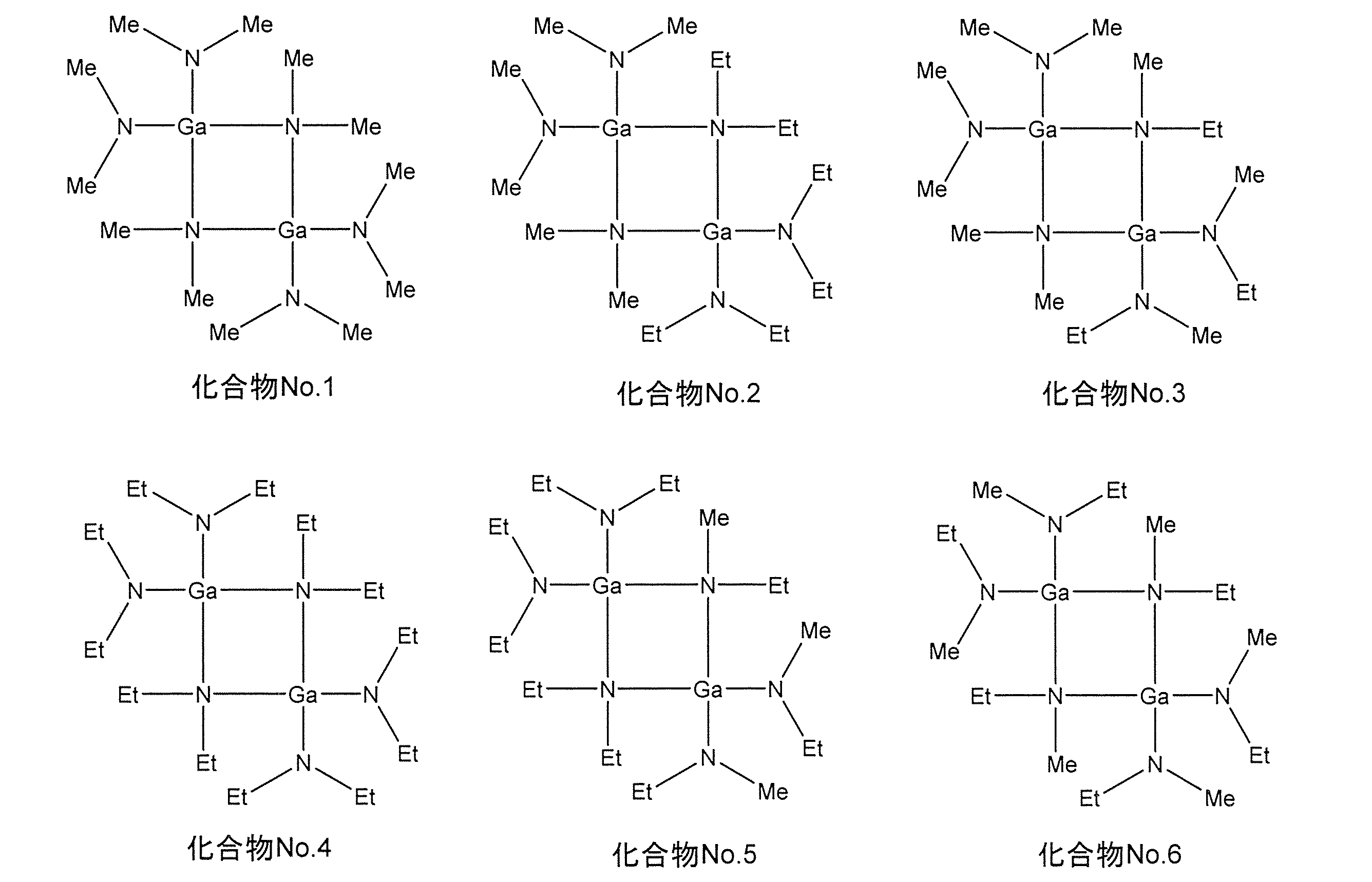
- gallium compound represented by the general formula (1) examples include the following compound No. 1 to No. 6 is mentioned.
- compound No. 1 to No. In 6 “Me” represents a methyl group and “Et” represents an ethyl group.
- the gallium compound represented by the general formula (1) is not particularly limited by the production method, and can be produced by a well-known synthetic method.
- the gallium compound represented by the general formula (1) can be obtained by, for example, reacting gallium chloride with a dialkylamine halide by a Grignard reaction.
- the raw material for forming a thin film of the present invention may be any as long as it contains the gallium compound represented by the general formula (1), and its composition varies depending on the type of the desired thin film. For example, when a thin film containing only gallium as a metal is produced, the thin film forming raw material of the present invention does not contain a metal compound and a semimetal compound other than the gallium compound represented by the general formula (1). On the other hand, when a thin film containing gallium and a metal and/or a semimetal other than gallium is produced, the thin film forming raw material of the present invention contains a gallium compound other than gallium in addition to the gallium compound represented by the general formula (1).
- the compound containing a metal and/or the compound containing a semimetal (hereinafter, also referred to as other precursor).
- the raw material for forming a thin film of the present invention may further contain an organic solvent and/or a nucleophilic reagent as described later.
- the form of the raw material for forming a thin film of the present invention is appropriately selected depending on the method such as the transport supply method of the atomic layer deposition method used.
- the thin film forming raw material of the present invention is vaporized by heating and/or depressurizing it in a container (hereinafter, also simply referred to as “raw material container”) in a container.
- a gas that introduces the vapor into a film forming chamber in which a substrate is installed hereinafter, also referred to as a "deposition reaction section" together with a carrier gas such as argon, nitrogen, or helium that is used as necessary.
- Transport method transporting the thin film forming raw material of the present invention in a liquid or solution state to a vaporization chamber, and vaporizing by vaporizing by heating and/or depressurizing in the vaporization chamber, and introducing the vapor into the film forming chamber
- a liquid transportation method In the case of the gas transport method, the gallium compound itself represented by the general formula (1) can be used as the raw material for forming a gallium nitride-containing thin film for the atomic layer deposition method.
- the gallium compound itself represented by the general formula (1) or a solution obtained by dissolving the gallium compound in an organic solvent can be used as a raw material for forming a gallium nitride-containing thin film for the atomic layer deposition method.
- These gallium nitride-containing thin film forming raw materials for atomic layer deposition may further contain other precursors, nucleophilic reagents and the like.
- the multi-component ALD method a method of vaporizing and supplying a raw material for forming a gallium nitride-containing thin film for an atomic layer deposition method independently of each component (hereinafter, also referred to as “single source method”), There is a method of vaporizing and supplying a mixed raw material in which multi-component raw materials are mixed in a desired composition in advance (hereinafter, also referred to as “cocktail sauce method”).
- a mixture of the gallium compound represented by the general formula (1) and another precursor or a mixed solution obtained by dissolving the mixture in an organic solvent is used as a raw material for forming a gallium nitride-containing thin film for the atomic layer deposition method. can do.
- This mixture or mixed solution may further contain a nucleophilic reagent or the like.
- organic solvent is not particularly limited, and well-known general organic solvents can be used.
- organic solvent include acetic acid esters such as ethyl acetate, butyl acetate and methoxyethyl acetate; ethers such as tetrahydrofuran, tetrahydropyran, ethylene glycol dimethyl ether, diethylene glycol dimethyl ether, triethylene glycol dimethyl ether, dibutyl ether and dioxane; methyl.
- Ketones such as butyl ketone, methyl isobutyl ketone, ethyl butyl ketone, dipropyl ketone, diisobutyl ketone, methyl amyl ketone, cyclohexanone, methylcyclohexanone; hexane, cyclohexane, methylcyclohexane, dimethylcyclohexane, ethylcyclohexane, heptane, octane, toluene, Hydrocarbons such as xylene; 1-cyanopropane, 1-cyanobutane, 1-cyanohexane, cyanocyclohexane, cyanobenzene, 1,3-dicyanopropane, 1,4-dicyanobutane, 1,6-dicyanohexane, 1, Hydrocarbons having a cyano group such as 4-dicyanocyclohexane and 1,4-d
- organic solvents may be used alone or in combination of two or more, depending on the solubility of the solute, the relationship between the use temperature and the boiling point, the flash point, and the like.
- the total amount of the precursor in the raw material which is a solution prepared by dissolving the precursor in the organic solvent, is 0.01 mol/liter to 2.0 mol/liter, particularly 0.05 mol/liter to 1 It is preferably adjusted to be 0.0 mol/liter.
- the raw material for forming a thin film of the present invention does not contain a metal compound and a metalloid compound other than the gallium compound represented by the general formula (1), the amount of the whole precursor is the amount of the gallium compound.
- the raw material for forming a thin film of the present invention contains a compound containing another metal and/or a compound containing a metalloid (another precursor) in addition to the gallium compound, the total amount of the gallium compound and the other precursor. Is.
- the other precursor used together with the gallium compound represented by the general formula (1) is not particularly limited and is used as a raw material for forming a thin film for the atomic layer deposition method.
- Known general precursors can be used.
- Other precursors include one or more selected from the group consisting of compounds used as organic ligands such as alcohol compounds, glycol compounds, ⁇ -diketone compounds, cyclopentadiene compounds and organic amine compounds, and silicon or metal. Compounds.
- precursor metal species include lithium, sodium, potassium, magnesium, calcium, strontium, barium, titanium, zirconium, hafnium, vanadium, niobium, tantalum, chromium, molybdenum, tungsten, manganese, iron, ruthenium, cobalt, rhodium.
- Iridium Iridium, nickel, palladium, platinum, copper, silver, gold, zinc, aluminum, indium, germanium, tin, lead, antimony, bismuth, scandium, ruthenium, yttrium, lanthanum, cerium, praseodymium, neodymium, promethium, samarium, europium , Gadolinium, terbium, dysprosium, holmium, erbium, thulium, ytterbium and lutetium.
- Alcohol compounds include alkyl alcohols such as methanol, ethanol, propanol, isopropyl alcohol, butanol, secondary butyl alcohol, isobutyl alcohol, tertiary butyl alcohol, pentyl alcohol, isopentyl alcohol and tertiary pentyl alcohol; 2-methoxyethanol , 2-ethoxyethanol, 2-butoxyethanol, 2-(2-methoxyethoxy)ethanol, 2-methoxy-1-methylethanol, 2-methoxy-1,1-dimethylethanol, 2-ethoxy-1,1-dimethyl Ethanol, 2-isopropoxy-1,1-dimethylethanol, 2-butoxy-1,1-dimethylethanol, 2-(2-methoxyethoxy)-1,1-dimethylethanol, 2-propoxy-1,1-diethyl Ether alcohols such as ethanol, 2-s-butoxy-1,1-diethylethanol, 3-methoxy-1,1-dimethylpropanol; dimethylaminoethanol, e
- glycol compound 1,2-ethanediol, 1,2-propanediol, 1,3-propanediol, 2,4-hexanediol, 2,2-dimethyl-1,3-propanediol, 2,2- Diethyl-1,3-propanediol, 1,3-butanediol, 2,4-butanediol, 2,2-diethyl-1,3-butanediol, 2-ethyl-2-butyl-1,3-propanediol , 2,4-pentanediol, 2-methyl-1,3-propanediol, 2-methyl-2,4-pentanediol, 2,4-hexanediol, 2,4-dimethyl-2,4-pentanediol, etc. Is mentioned.
- ⁇ -diketone compounds include acetylacetone, hexane-2,4-dione, 5-methylhexane-2,4-dione, heptane-2,4-dione, 2-methylheptane-3,5-dione, 5-methyl Heptane-2,4-dione, 6-methylheptane-2,4-dione, 2,2-dimethylheptane-3,5-dione, 2,6-dimethylheptane-3,5-dione, 2,2,6 -Trimethylheptane-3,5-dione, 2,2,6,6-tetramethylheptane-3,5-dione, octane-2,4-dione, 2,2,6-trimethyloctane-3,5-dione 2,6-dimethyloctane-3,5-dione, 2,9-dimethylnonane-4,6-dione, 2-methyl-6-ethyldecane-3,
- cyclopentadiene compound examples include cyclopentadiene, methylcyclopentadiene, ethylcyclopentadiene, propylcyclopentadiene, isopropylcyclopentadiene, butylcyclopentadiene, tert-butylcyclopentadiene, isobutylcyclopentadiene, tert-butylcyclopentadiene, dimethylcyclopentadiene, tetra Methylcyclopentadiene and the like can be mentioned.
- organic amine compound examples include methylamine, ethylamine, propylamine, isopropylamine, butylamine, sec-butylamine, sec-butylamine, isobutylamine, dimethylamine, diethylamine, dipropylamine, diisopropylamine, ethylmethylamine, propylmethylamine, Isopropylmethylamine and the like can be mentioned.
- the above-mentioned other precursors are known in the art, and their manufacturing methods are also known.
- the production method for example, when an alcohol compound is used as an organic ligand, the above-mentioned inorganic salt of a metal or a hydrate thereof is reacted with an alkali metal alkoxide of the alcohol compound. By doing so, the precursor can be manufactured.
- the inorganic salt of metal or its hydrate include metal halides and nitrates.
- the alkali metal alkoxide include sodium alkoxide, lithium alkoxide, potassium alkoxide and the like.
- a compound having a thermal and/or oxidative decomposition behavior similar to that of the gallium compound represented by the general formula (1) is preferable.
- other precursors are similar to the gallium compound represented by the above general formula (1) in behavior of heat and/or oxidative decomposition, and in addition, alteration due to chemical reaction during mixing is performed. Compounds that do not occur are preferred.
- the raw material for forming a thin film of the present invention may contain a nucleophilic reagent, if necessary, in order to improve the stability of the gallium compound represented by the general formula (1) and other precursors. ..
- the nucleophilic reagent include ethylene glycol ethers such as glyme, diglyme, triglyme, and tetraglyme, 18-crown-6, dicyclohexyl-18-crown-6, 24-crown-8, dicyclohexyl-24-crown-8.
- Crown ethers such as dibenzo-24-crown-8, ethylenediamine, N,N'-tetramethylethylenediamine, diethylenetriamine, triethylenetetramine, tetraethylenepentamine, pentaethylenehexamine, 1,1,4,7,7- Polyamines such as pentamethyldiethylenetriamine, 1,1,4,7,10,10-hexamethyltriethylenetetramine and triethoxytriethyleneamine, cyclic polyamines such as cyclam and cyclen, pyridine, pyrrolidine, piperidine, morpholine, N Heterocyclic compounds such as -methylpyrrolidine, N-methylpiperidine, N-methylmorpholine, tetrahydrofuran, tetrahydropyran, 1,4-dioxane, oxazole, thiazole, oxathiolane, methyl acetoacetate, ethyl acetoacetate, acetoacetic acid-2- Examples
- the raw material for forming a thin film of the present invention should contain as much as possible impurities metal element components other than the constituent components thereof, impurity halogen components such as impurity chlorine, and impurity organic components.
- the impurity metal element content is preferably 100 ppb or less for each element, more preferably 10 ppb or less, and total amount is preferably 1 ppm or less, more preferably 100 ppb or less.
- it is necessary to reduce the content of alkali metal elements and alkaline earth metal elements that affect the electrical characteristics of the obtained thin film.
- the impurity halogen content is preferably 100 ppm or less, more preferably 10 ppm or less, most preferably 1 ppm or less.
- the total amount of organic impurities is preferably 500 ppm or less, more preferably 50 ppm or less, most preferably 10 ppm or less.
- the precursor, the organic solvent and the nucleophilic reagent are used to reduce the respective water contents. In addition, it is better to remove water as much as possible before use.
- the water content of each of the precursor, organic solvent and nucleophilic reagent is preferably 10 ppm or less, more preferably 1 ppm or less.
- the thin film forming raw material of the present invention does not contain particles as much as possible in order to reduce or prevent particle contamination of the formed thin film.
- the number of particles larger than 0.3 ⁇ m is preferably 100 or less in 1 mL of the liquid phase, and larger than 0.2 ⁇ m. More preferably, the number of particles is 1000 or less in 1 mL of the liquid phase, and most preferably the number of particles larger than 0.2 ⁇ m is 100 or less in 1 mL of the liquid phase.
- the method for producing a gallium nitride-containing thin film of the present invention is characterized by forming a thin film by the ALD method using the above-mentioned thin film forming raw material.
- the method of producing a gallium nitride-containing thin film on the surface of a substrate by the ALD method according to the present invention includes the steps of introducing into a film forming chamber in which a substrate is installed, and then decomposing and/or chemically reacting a gallium compound on the substrate to grow and deposit a thin film containing gallium nitride on the surface of the substrate.
- Examples of the material of the base include silicon; ceramics such as silicon nitride, titanium nitride, tantalum nitride, titanium oxide, titanium nitride, ruthenium oxide, zirconium oxide, hafnium oxide, and lanthanum oxide; glass; metals such as metallic cobalt.
- Examples of the shape of the substrate include a plate shape, a spherical shape, a fibrous shape, and a scaly shape.
- the surface of the substrate may be flat or may have a three-dimensional structure such as a trench structure.
- Examples of the above-mentioned reactive gas include reducing gas such as hydrogen, organic amine compounds such as monoalkylamine, dialkylamine, trialkylamine and alkylenediamine, and nitriding gas such as hydrazine and ammonia. These reactive gases may be used alone or in combination of two or more.
- the gallium compound represented by the general formula (1) has a property of reacting well with ammonia, hydrazine and hydrogen, and has a property of reacting particularly well with ammonia. Therefore, it is preferable to use ammonia as the reactive gas.
- the above manufacturing conditions include the temperature and pressure at which the thin film forming raw material of the present invention is vaporized into steam.
- the step of vaporizing the raw material for forming a thin film of the present invention into vapor may be performed in the raw material container or in the vaporization chamber.
- the thin film forming raw material of the present invention is preferably evaporated at 0°C to 200°C.
- both the pressure in the raw material container and the pressure in the vaporization chamber are preferably 1 Pa to 10000 Pa.
- reaction temperature substrate temperature
- reaction pressure reaction pressure
- deposition rate deposition rate
- the reaction temperature is set within an ALD window matched to the reactive gas, but is preferably 100° C. or higher at which the gallium compound represented by the general formula (1) sufficiently reacts, and 100° C. to 250° C. More preferable.
- ammonia is used as the reactive gas, it is preferable that the temperature is in the range of 120° C. to 200° C. because a gallium nitride-containing thin film with less residual carbon and good quality can be produced with good productivity.
- each step of the ALD method will be described in detail by taking an example of forming a gallium nitride thin film using ammonia gas as a reactive gas.
- the vapor of the thin film forming raw material of the present invention is introduced into the film forming chamber (raw material introducing step).
- the preferable temperature and pressure when the raw material for forming a thin film of the present invention is vaporized are in the range of 0° C. to 200° C. and 1 Pa to 10000 Pa.
- the vapor introduced into the film forming chamber is deposited on the surface of the substrate to form a precursor thin film on the surface of the substrate (precursor thin film forming step).
- the substrate may be heated, or the processing atmosphere in the film forming chamber may be heated.
- the temperature of the substrate or the temperature of the treatment atmosphere when this step is performed is preferably room temperature to 250°C, more preferably 100°C to 250°C.
- the ALD window is generally in the range of 120°C to 200°C.
- the pressure of the system (in the film forming chamber) when this step is performed is preferably 1 Pa to 10000 Pa, more preferably 10 Pa to 1000 Pa.
- the unreacted thin film forming material vapor and by-produced gas are exhausted from the film forming chamber (exhaust process).
- the unreacted thin film forming raw material vapor and the by-product gas are ideally completely exhausted from the film forming chamber, but they are not necessarily completely exhausted.
- Examples of the exhaust method include a method of purging the system with an inert gas such as nitrogen, helium, and argon, a method of exhausting by depressurizing the system, and a method of combining these.
- the degree of pressure reduction is preferably 0.01 Pa to 300 Pa, more preferably 0.01 Pa to 100 Pa.
- ammonia gas is introduced as a reactive gas into the film forming chamber, and the gallium nitride-containing thin film is formed from the precursor thin film formed in the precursor thin film forming step by the action of ammonia gas or the action of ammonia gas and heat.
- Forming (gallium nitride-containing thin film forming step).
- the temperature when heat is applied in this step is preferably room temperature to 250°C, more preferably 100°C to 250°C.
- the ALD window is generally in the range of 120° C. to 200° C. Therefore, it is preferable to react the precursor thin film with ammonia gas within this temperature range. ..
- the pressure of the system (in the film forming chamber) when this step is performed is preferably 1 Pa to 10000 Pa, more preferably 10 Pa to 1000 Pa.
- thin film deposition by a series of operations including the above raw material introducing step, precursor thin film forming step, evacuation step and gallium nitride containing thin film forming step is defined as one cycle, and this cycle is It may be repeated several times until a thin film having a required film thickness is obtained. In this case, after carrying out one cycle, it is preferable to carry out the next one cycle after exhausting the unreacted reactive gas and the by-produced gas from the film forming chamber in the same manner as the exhaust step.
- the method for producing a gallium nitride-containing thin film of the present invention energy such as light and voltage may be applied, or a catalyst may be used.
- the timing of applying the energy and the timing of using the catalyst are not particularly limited. For example, at the time of introducing the vapor of the raw material for forming a thin film for the atomic layer deposition method in the raw material introducing step, the precursor thin film forming step or the gallium nitride-containing thin film.
- the heating may be performed in the forming step, the system may be exhausted in the exhausting step, the reactive gas may be introduced in the gallium nitride-containing thin film forming step, or the above steps may be performed.
- an annealing treatment is performed under an inert atmosphere, an oxidizing atmosphere or a reducing atmosphere in order to obtain better electric characteristics.
- a reflow process may be provided when step filling is required.
- the temperature is 200°C to 1000°C, preferably 250°C to 500°C.
- a well-known device for atomic layer deposition can be used as a device for producing a gallium nitride-containing thin film using the thin film forming raw material of the present invention.
- the apparatus include an apparatus capable of bubbling and supplying a precursor as shown in FIG. 1 and an apparatus having a vaporization chamber as shown in FIG. Not only the single-wafer type apparatus as shown in FIGS. 1 and 2, but also an apparatus capable of simultaneously processing a large number of sheets using a batch furnace can be used.
- This gallium chloride solution was slowly added dropwise to the above-mentioned suspension of lithium dimethylamide, and the mixture was reacted overnight at room temperature. Then, the mixture was heated and stirred at 80° C. for 8 hours. After allowing to cool, the reaction solution was filtered with a 0.2 ⁇ m membrane filter to collect the filtrate. The solvent is removed from the filtrate under an argon atmosphere at an oil bath temperature of 80°C to 100°C at atmospheric pressure to a slight reduced pressure, and then heated at an oil bath temperature of 100°C to 120°C under reduced pressure until a white solid precipitates. Dried.
- a white solid was purified by sublimation at a pressure of 40 Pa and an oil bath temperature of 125°C to obtain a target substance (trisdimethylamide gallium (III)) as a white solid (melting point 102°C).
- the yield was 2.6 g, and the yield was 65%.
- This gallium chloride solution was slowly added dropwise to the above-mentioned suspension of lithium ethylmethylamide under ice-cooling conditions, and the mixture was reacted at room temperature overnight. Then, the mixture was heated and stirred at 50° C. for 8 hours. After allowing to cool, the reaction solution was filtered with a 0.2 ⁇ m membrane filter and the filtrate was collected. The solvent is removed from the filtrate under an argon atmosphere at an oil bath temperature of 80°C to 100°C at atmospheric pressure to a slight reduced pressure, and then heated and dried at an oil bath temperature of 100°C to 120°C under reduced pressure to obtain a viscous liquid.
- the viscous liquid obtained was purified by distillation at a pressure of 10 Pa to 15 Pa and an oil bath temperature of 140° C. to obtain the target product (trisethylmethylamide gallium (III)) as a pale yellow liquid.
- the yield was 1.0 g, and the yield was 50%.
- Example 1 Production of gallium nitride thin film Compound No. Using No. 1 as a raw material for forming a thin film, a gallium nitride thin film was produced on a silicon wafer by the ALD method under the following conditions using the apparatus shown in FIG.
- the composition of the obtained thin film was confirmed by X-ray photoelectron spectroscopy, the obtained thin film was gallium nitride, and the residual carbon content was less than 0.1 atom %. Further, when the film thickness was measured by the X-ray reflectance method and the average value was calculated, the film thickness was 10 nm on average, and the film thickness obtained per cycle was 0.20 nm on average.
- Substrate Silicon wafer Reaction temperature (silicon wafer temperature): 150°C Reactive gas: Ammonia
- the material for forming a thin film which is vaporized under the conditions of the temperature of the raw material container: 100° C. and the pressure in the raw material container: 100 Pa, is introduced into the film forming chamber and deposited at a system pressure of 100 Pa for 30 seconds.
- Argon purge for 15 seconds removes the thin film forming raw material that has not deposited.
- a reactive gas is introduced into the film forming chamber, and the reaction is performed for 60 seconds at a system pressure of 100 Pa. (4) Unreacted reactive gas and by-product gas are removed by argon purge for 15 seconds.
- Example 2 Production of gallium nitride thin film Compound No. 3 was used as a raw material for forming a thin film.
- a gallium nitride thin film was manufactured under the same conditions as in Example 1 except that No. 6 was used.
- the composition of the thin film was confirmed by X-ray photoelectron spectroscopy, the obtained thin film was gallium nitride and the residual carbon content was 1.0 atom %.
- the film thickness was measured by the X-ray reflectance method, and the average value was calculated. The film thickness was 6.5 nm on average, and the film thickness obtained per cycle was 0.13 nm on average.
- Example 1 Production of gallium nitride thin film A gallium nitride thin film was produced under the same conditions as in Example 1 except that the following comparative compound 1 was used as a raw material for forming a thin film.
- the composition of the obtained thin film was confirmed by X-ray photoelectron spectroscopy, the obtained thin film was a mixture in which gallium nitride and gallium carbide were formed nonuniformly, and the residual carbon content was 20.0 atom%. Met.
- the film thickness was measured by the X-ray reflectance method and the average value was calculated, the film thickness was 1.5 nm on average, and the film thickness obtained per cycle was 0.030 nm on average.
- Example 2 Production of gallium nitride thin film A gallium nitride thin film was produced under the same conditions as in Example 1 except that the following comparative compound 2 ("iPr" represents an isopropyl group) was used as a raw material for forming a thin film.
- the composition of the obtained thin film was confirmed by X-ray photoelectron spectroscopy, the obtained thin film was a mixture in which gallium nitride and gallium carbide were formed nonuniformly, and the residual carbon content was 25.0 atom%. Met. Further, when the film thickness was measured by the X-ray reflectance method and the average value was calculated, the film thickness was 5.0 nm on average, and the film thickness obtained per cycle was 0.10 nm on average.
- Example 1 From the results of Examples 1 and 2, it was possible to manufacture a high-quality gallium nitride thin film having a low residual carbon content without requiring a step of plasma irradiation. Among them, it was found that the gallium nitride thin film obtained in Example 1 had a very low residual carbon content and was a particularly good quality gallium nitride thin film. On the other hand, in Comparative Examples 1 and 2, the residual carbon content of the obtained thin film was 20 atom% or more, so that the quality was poor, and the gallium nitride and the gallium carbide were nonuniformly formed. A good gallium nitride thin film could not be obtained.
Landscapes
- Chemical & Material Sciences (AREA)
- General Chemical & Material Sciences (AREA)
- Chemical Kinetics & Catalysis (AREA)
- Engineering & Computer Science (AREA)
- Materials Engineering (AREA)
- Mechanical Engineering (AREA)
- Metallurgy (AREA)
- Organic Chemistry (AREA)
- Inorganic Chemistry (AREA)
- Chemical Vapour Deposition (AREA)
Abstract
下記一般式(1)で表されるガリウム化合物を含有する原子層堆積法用窒化ガリウム含有薄膜形成用原料。 (式中、R1~R4は、それぞれ独立にメチル基又はエチル基を表す。)
Description
本発明は、特定の構造を有するガリウム化合物を含有する原子層堆積法用窒化ガリウム含有薄膜形成用原料及び窒化ガリウム含有薄膜の製造方法に関する。
窒化ガリウム含有薄膜は、特異的な電気特性を示す。そのため、窒化ガリウム含有薄膜は、半導体材料、発光ダイオードの材料等の種々の用途に応用されている。
薄膜の製造法としては、例えばスパッタリング法、イオンプレーティング法、塗布熱分解法やゾルゲル法等のMOD法、CVD法等が挙げられる。これらの中でも、組成制御性及び段差被覆性に優れること、量産化に適すること、ハイブリッド集積が可能である等多くの長所を有しているので、原子層堆積法(以下、ALD法という場合がある)が最適な製造プロセスである。
CVD法及びALD法のような気相薄膜形成法に用いることができる材料は種々報告されている。ALD法に適用可能な薄膜形成用原料は、ALDウィンドウと呼ばれる温度領域が十分な広さであることが必要である。そのため、CVD法に使用可能な薄膜形成用原料であっても、ALD法に適さない場合が多くあることは当該技術分野における技術常識とされている。
ALD法用原料として用いられるガリウム化合物として、様々なガリウム化合物が知られている。例えば、特許文献1~4には、トリメチルガリウム、トリエチルガリウム等のトリアルキルガリウム、トリス(ジメチルアミノ)ガリウム、トリス(ジエチルアミノ)ガリウム等のトリス(ジアルキルアミノ)ガリウムが開示されている。非特許文献1には、トリス(ジアルキルアミノ)ガリウムを原料として用いたALD法で硫化ガリウムを製造したことが開示されている。非特許文献2には、トリス(ジアルキルアミノ)ガリウムを原料として用いたALD法で酸化ガリウムを製造したことが開示されている。非特許文献3には、トリメチルガリウムを原料として用いたALD法で窒化ガリウムを製造したことが開示されている。
Journal of Physical Chemistry C (2017), 121(11), 5871-5881
Dalton Transactions (2017), 46(47), 16551-16561
Applied Surface Science (2015), 357(Part B), 1920-1927
しかしながら、ALD法を用いて品質の良い窒化ガリウムを形成することは非常に難しい。非特許文献3に記載されるように、トリメチルガリウムを原料として用いたALD法では、工程中にプラズマを照射する必要がある。プラズマの照射により基体及び周辺部材が損傷を受けるため、プラズマを照射せずに窒化ガリウム薄膜を形成する方法が望まれていた。
従って、本発明は、プラズマを照射することなく、品質の良い窒化ガリウム含有薄膜を形成することができる原子層堆積法用薄膜形成用原料及びその原料を用いた薄膜の製造方法を提供することを目的とする。
本発明者らは、検討を重ねた結果、原子層堆積法用薄膜形成用原料として特定の構造を有するガリウム化合物を用いることにより上記課題を解決し得ることを知見し、本発明を完成するに到った。
即ち、本発明は、下記一般式(1)で表されるガリウム化合物を含有する、原子層堆積法用窒化ガリウム含有薄膜形成用原料である。
即ち、本発明は、下記一般式(1)で表されるガリウム化合物を含有する、原子層堆積法用窒化ガリウム含有薄膜形成用原料である。
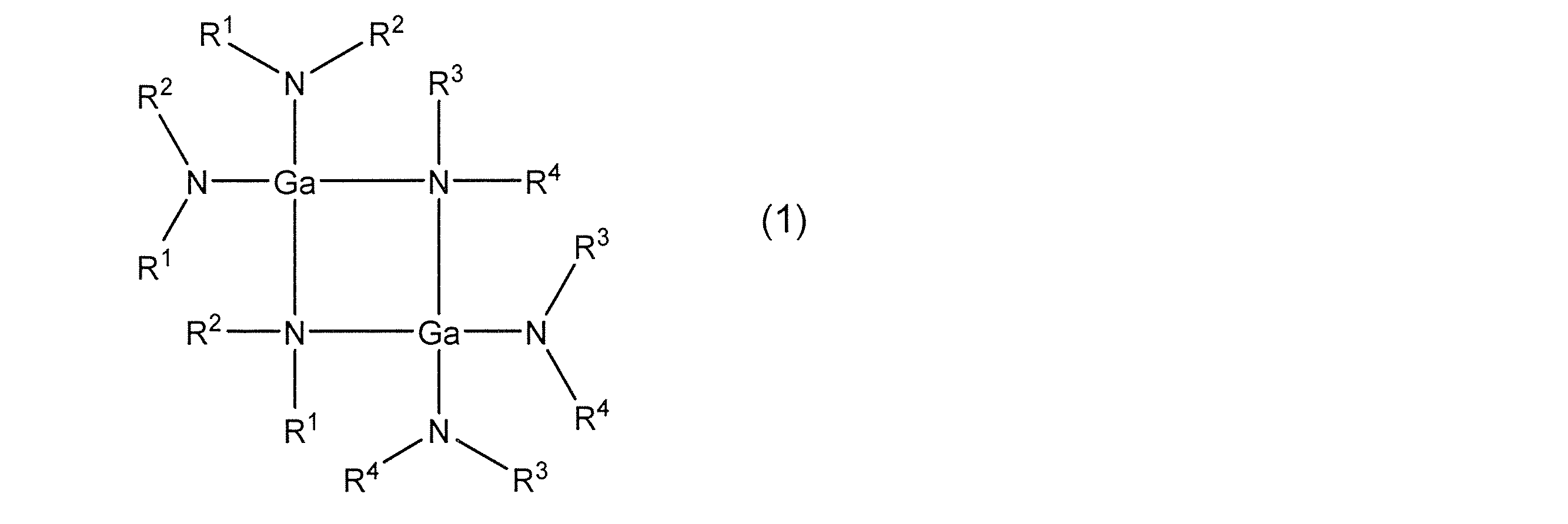
(式中、R1~R4は、それぞれ独立にメチル基又はエチル基を表す。)
また、本発明は、基体の表面に窒化ガリウム含有薄膜を原子層堆積法により製造する方法であって、上記原子層堆積法用窒化ガリウム含有薄膜形成用原料を気化させてガリウム化合物を含有する蒸気を得る工程と、前記蒸気を処理雰囲気中に導入する工程と、前記ガリウム化合物を分解及び/又は化学反応させて前記基体の表面に前記ガリウム化合物を堆積させる工程とを含む窒化ガリウム含有薄膜の製造方法である。
本発明によれば、プラズマを照射することなく、品質の良い窒化ガリウム含有薄膜を原子層堆積法により生産性良く製造することができる薄膜形成用原料を提供することができる。また、本発明によれば、品質の良い窒化ガリウム含有薄膜を生産性良く製造することができる薄膜の製造方法を提供することができる。
本発明の原子層堆積法用窒化ガリウム含有薄膜形成用原料(以下、本発明の薄膜形成用原料という場合がある)は、上記一般式(1)で表されるガリウム化合物を含有することを特徴とする。
本明細書における「窒化ガリウム含有薄膜」とは、窒化ガリウムを含有する薄膜であればよく特に限定されるものではないが、例えば、窒化ガリウム薄膜、窒化ガリウムとアルミニウム、マンガン、インジウム等の金属とが合金化したもの、窒化ガリウム薄膜にランタン等の希土類原子がドープされたもの等を挙げることができる。
上記一般式(1)において、R1~R4は、それぞれ独立にメチル基又はエチル基を表す。
残留炭素が非常に少なく品質の良い窒化ガリウム含有薄膜を得ることができるという点から、上記一般式(1)において、R1及びR3がメチル基であり且つR2及びR4がメチル基又はエチル基であるガリウム化合物が好ましく、R1~R4がメチル基であるガリウム化合物が特に好ましい。
上記一般式(1)で表されるガリウム化合物の好ましい具体例としては、例えば、下記化合物No.1~No.6が挙げられる。なお、下記化合物No.1~No.6において、「Me」はメチル基を表し、「Et」はエチル基を表す。
上記一般式(1)で表されるガリウム化合物は、その製造方法により特に制限されることはなく、周知の合成方法で製造される。上記一般式(1)で表されるガリウム化合物の製造方法としては、例えば、塩化ガリウムとハロゲン化ジアルキルアミンとをグリニャール反応させることで得ることができる。
本発明の薄膜形成用原料は、上記一般式(1)で表されるガリウム化合物を含有するものであればよく、その組成は、目的とする薄膜の種類によって異なる。例えば、金属としてガリウムのみを含む薄膜を製造する場合、本発明の薄膜形成用原料は、上記一般式(1)で表されるガリウム化合物以外の金属化合物及び半金属化合物を非含有である。一方、ガリウムと、ガリウム以外の金属及び/又は半金属とを含む薄膜を製造する場合、本発明の薄膜形成用原料は、上記一般式(1)で表されるガリウム化合物に加えて、ガリウム以外の金属を含む化合物及び/又は半金属を含む化合物(以下、他のプレカーサともいう)を含有する。本発明の薄膜形成用原料は、後述するように、更に、有機溶剤及び/又は求核性試薬を含有してもよい。
本発明の薄膜形成用原料の形態は使用される原子層堆積法の輸送供給方法等の手法により適宜選択されるものである。
上記の輸送供給方法としては、本発明の薄膜形成用原料が貯蔵される容器(以下、単に「原料容器」と記載することもある)中で加熱及び/又は減圧することにより気化させて蒸気とし、必要に応じて用いられるアルゴン、窒素、ヘリウム等のキャリアガスと共に、該蒸気を基体が設置された成膜チャンバー内(以下、「堆積反応部」と記載することもある)へと導入する気体輸送法、本発明の薄膜形成用原料を液体又は溶液の状態で気化室まで輸送し、気化室で加熱及び/又は減圧することにより気化させて蒸気とし、該蒸気を成膜チャンバー内へと導入する液体輸送法がある。気体輸送法の場合は、上記一般式(1)で表されるガリウム化合物そのものを原子層堆積法用窒化ガリウム含有薄膜形成用原料とすることができる。液体輸送法の場合は、上記一般式(1)で表されるガリウム化合物そのもの又は該ガリウム化合物を有機溶剤に溶かした溶液を原子層堆積法用窒化ガリウム含有薄膜形成用原料とすることができる。これらの原子層堆積法用窒化ガリウム含有薄膜形成用原料は、他のプレカーサ、求核性試薬等を更に含んでもよい。
また、多成分系のALD法においては、原子層堆積法用窒化ガリウム含有薄膜形成用原料を各成分独立で気化、供給する方法(以下、「シングルソース法」と記載することもある)と、多成分原料を予め所望の組成で混合した混合原料を気化、供給する方法(以下、「カクテルソース法」と記載することもある)がある。カクテルソース法の場合、上記一般式(1)で表されるガリウム化合物と他のプレカーサとの混合物若しくは該混合物を有機溶剤に溶かした混合溶液を原子層堆積法用窒化ガリウム含有薄膜形成用原料とすることができる。この混合物や混合溶液は、求核性試薬等を更に含んでいてもよい。
上記の有機溶剤としては、特に制限を受けることはなく周知一般の有機溶剤を用いることができる。該有機溶剤としては、例えば、酢酸エチル、酢酸ブチル、酢酸メトキシエチル等の酢酸エステル類;テトラヒドロフラン、テトラヒドロピラン、エチレングリコールジメチルエーテル、ジエチレングリコールジメチルエーテル、トリエチレングリコールジメチルエーテル、ジブチルエーテル、ジオキサン等のエーテル類;メチルブチルケトン、メチルイソブチルケトン、エチルブチルケトン、ジプロピルケトン、ジイソブチルケトン、メチルアミルケトン、シクロヘキサノン、メチルシクロヘキサノン等のケトン類;ヘキサン、シクロヘキサン、メチルシクロヘキサン、ジメチルシクロヘキサン、エチルシクロヘキサン、ヘプタン、オクタン、トルエン、キシレン等の炭化水素類;1-シアノプロパン、1-シアノブタン、1-シアノヘキサン、シアノシクロヘキサン、シアノベンゼン、1,3-ジシアノプロパン、1,4-ジシアノブタン、1,6-ジシアノヘキサン、1,4-ジシアノシクロヘキサン、1,4-ジシアノベンゼン等のシアノ基を有する炭化水素類;ピリジン、ルチジン等が挙げられる。これらの有機溶剤は、溶質の溶解性、使用温度と沸点、引火点の関係等により、単独で用いてもよいし、又は二種類以上を混合して用いてもよい。これらの有機溶剤を使用する場合、プレカーサを有機溶剤に溶かした溶液である原料中におけるプレカーサ全体の量が0.01モル/リットル~2.0モル/リットル、特に0.05モル/リットル~1.0モル/リットルとなるようにするのが好ましい。プレカーサ全体の量とは、本発明の薄膜形成用原料が、上記一般式(1)で表されるガリウム化合物以外の金属化合物及び半金属化合物を非含有である場合、該ガリウム化合物の量であり、本発明の薄膜形成用原料が、該ガリウム化合物に加えて他の金属を含む化合物及び/又は半金属を含む化合物(他のプレカーサ)を含有する場合、該ガリウム化合物及び他のプレカーサの合計量である。
また、多成分系のALD法の場合において、上記一般式(1)で表されるガリウム化合物と共に用いられる他のプレカーサとしては、特に制限を受けず、原子層堆積法用薄膜形成用原料に用いられている周知一般のプレカーサを用いることができる。
他のプレカーサとしては、アルコール化合物、グリコール化合物、β-ジケトン化合物、シクロペンタジエン化合物、有機アミン化合物等の有機配位子として用いられる化合物からなる群から選択される一種類以上とケイ素又は金属との化合物が挙げられる。
他のプレカーサの金属種としては、リチウム、ナトリウム、カリウム、マグネシウム、カルシウム、ストロンチウム、バリウム、チタニウム、ジルコニウム、ハフニウム、バナジウム、ニオブ、タンタル、クロム、モリブデン、タングステン、マンガン、鉄、ルテニウム、コバルト、ロジウム、イリジウム、ニッケル、パラジウム、白金、銅、銀、金、亜鉛、アルミニウム、インジウム、ゲルマニウム、スズ、鉛、アンチモン、ビスマス、スカンジウム、ルテニウム、イットリウム、ランタン、セリウム、プラセオジム、ネオジム、プロメチウム、サマリウム、ユウロピウム、ガドリニウム、テルビウム、ジスプロシウム、ホルミウム、エルビウム、ツリウム、イッテルビウム及びルテチウムが挙げられる。
アルコール化合物としては、メタノール、エタノール、プロパノール、イソプロピルアルコール、ブタノール、第2ブチルアルコール、イソブチルアルコール、第3ブチルアルコール、ペンチルアルコール、イソペンチルアルコール、第3ペンチルアルコール等のアルキルアルコール類;2-メトキシエタノール、2-エトキシエタノール、2-ブトキシエタノール、2-(2-メトキシエトキシ)エタノール、2-メトキシ-1-メチルエタノール、2-メトキシ-1,1-ジメチルエタノール、2-エトキシ-1,1-ジメチルエタノール、2-イソプロポキシ-1,1-ジメチルエタノール、2-ブトキシ-1,1-ジメチルエタノール、2-(2-メトキシエトキシ)-1,1-ジメチルエタノール、2-プロポキシ-1,1-ジエチルエタノール、2-s-ブトキシ-1,1-ジエチルエタノール、3-メトキシ-1,1-ジメチルプロパノール等のエーテルアルコール類;ジメチルアミノエタノール、エチルメチルアミノエタノール、ジエチルアミノエタノール、ジメチルアミノ-2-ペンタノール、エチルメチルアミノ-2-ペンタノール、ジメチルアミノ-2-メチル-2-ペンタノール、エチルメチルアミノ-2-メチル-2-ペンタノール、ジエチルアミノ-2-メチル-2-ペンタノール等のジアルキルアミノアルコール類等が挙げられる。
グリコール化合物としては、1,2-エタンジオール、1,2-プロパンジオール、1,3-プロパンジオール、2,4-ヘキサンジオール、2,2-ジメチル-1,3-プロパンジオール、2,2-ジエチル-1,3-プロパンジオール、1,3-ブタンジオール、2,4-ブタンジオール、2,2-ジエチル-1,3-ブタンジオール、2-エチル-2-ブチル-1,3-プロパンジオール、2,4-ペンタンジオール、2-メチル-1,3-プロパンジオール、2-メチル-2,4-ペンタンジオール、2,4-ヘキサンジオール、2,4-ジメチル-2,4-ペンタンジオール等が挙げられる。
β-ジケトン化合物としては、アセチルアセトン、ヘキサン-2,4-ジオン、5-メチルヘキサン-2,4-ジオン、ヘプタン-2,4-ジオン、2-メチルヘプタン-3,5-ジオン、5-メチルヘプタン-2,4-ジオン、6-メチルヘプタン-2,4-ジオン、2,2-ジメチルヘプタン-3,5-ジオン、2,6-ジメチルヘプタン-3,5-ジオン、2,2,6-トリメチルヘプタン-3,5-ジオン、2,2,6,6-テトラメチルヘプタン-3,5-ジオン、オクタン-2,4-ジオン、2,2,6-トリメチルオクタン-3,5-ジオン、2,6-ジメチルオクタン-3,5-ジオン、2,9-ジメチルノナン-4,6-ジオン、2-メチル-6-エチルデカン-3,5-ジオン、2,2-ジメチル-6-エチルデカン-3,5-ジオン等のアルキル置換β-ジケトン類;1,1,1-トリフルオロペンタン-2,4-ジオン、1,1,1-トリフルオロ-5,5-ジメチルヘキサン-2,4-ジオン、1,1,1,5,5,5-ヘキサフルオロペンタン-2,4-ジオン、1,3-ジパーフルオロヘキシルプロパン-1,3-ジオン等のフッ素置換アルキルβ-ジケトン類;1,1,5,5-テトラメチル-1-メトキシヘキサン-2,4-ジオン、2,2,6,6-テトラメチル-1-メトキシヘプタン-3,5-ジオン、2,2,6,6-テトラメチル-1-(2-メトキシエトキシ)ヘプタン-3,5-ジオン等のエーテル置換β-ジケトン類等が挙げられる。
シクロペンタジエン化合物としては、シクロペンタジエン、メチルシクロペンタジエン、エチルシクロペンタジエン、プロピルシクロペンタジエン、イソプロピルシクロペンタジエン、ブチルシクロペンタジエン、第2ブチルシクロペンタジエン、イソブチルシクロペンタジエン、第3ブチルシクロペンタジエン、ジメチルシクロペンタジエン、テトラメチルシクロペンタジエン等が挙げられる。
有機アミン化合物としては、メチルアミン、エチルアミン、プロピルアミン、イソプロピルアミン、ブチルアミン、第2ブチルアミン、第3ブチルアミン、イソブチルアミン、ジメチルアミン、ジエチルアミン、ジプロピルアミン、ジイソプロピルアミン、エチルメチルアミン、プロピルメチルアミン、イソプロピルメチルアミン等が挙げられる。
上記した他のプレカーサは、当該技術分野において公知のものであり、その製造方法も公知である。製造方法の一例を挙げれば、例えば、有機配位子としてアルコール化合物を用いた場合には、先に述べた金属の無機塩又はその水和物と、該アルコール化合物のアルカリ金属アルコキシドとを反応させることによって、プレカーサを製造することができる。ここで、金属の無機塩又はその水和物としては、金属のハロゲン化物、硝酸塩等を挙げることができる。アルカリ金属アルコキシドとしては、ナトリウムアルコキシド、リチウムアルコキシド、カリウムアルコキシド等を挙げることができる。
シングルソース法の場合、他のプレカーサとしては、上記一般式(1)で表されるガリウム化合物と熱及び/又は酸化分解の挙動が類似している化合物が好ましい。カクテルソース法の場合、他のプレカーサとしては、上記一般式(1)で表されるガリウム化合物と熱及び/又は酸化分解の挙動が類似していることに加え、混合時に化学反応等による変質を起こさない化合物が好ましい。
また、本発明の薄膜形成用原料は、必要に応じて、上記一般式(1)で表されるガリウム化合物及び他のプレカーサの安定性を向上させるため、求核性試薬を含有してもよい。該求核性試薬としては、グライム、ジグライム、トリグライム、テトラグライム等のエチレングリコールエーテル類、18-クラウン-6、ジシクロヘキシル-18-クラウン-6、24-クラウン-8、ジシクロヘキシル-24-クラウン-8、ジベンゾ-24-クラウン-8等のクラウンエーテル類、エチレンジアミン、N,N’-テトラメチルエチレンジアミン、ジエチレントリアミン、トリエチレンテトラミン、テトラエチレンペンタミン、ペンタエチレンヘキサミン、1,1,4,7,7-ペンタメチルジエチレントリアミン、1,1,4,7,10,10-ヘキサメチルトリエチレンテトラミン、トリエトキシトリエチレンアミン等のポリアミン類、サイクラム、サイクレン等の環状ポリアミン類、ピリジン、ピロリジン、ピペリジン、モルホリン、N-メチルピロリジン、N-メチルピペリジン、N-メチルモルホリン、テトラヒドロフラン、テトラヒドロピラン、1,4-ジオキサン、オキサゾール、チアゾール、オキサチオラン等の複素環化合物類、アセト酢酸メチル、アセト酢酸エチル、アセト酢酸-2-メトキシエチル等のβ-ケトエステル類又はアセチルアセトン、2,4-ヘキサンジオン、2,4-ヘプタンジオン、3,5-ヘプタンジオン、ジピバロイルメタン等のβ-ジケトン類が挙げられる。これらの求核性試薬の使用量は、プレカーサ全体の量1モルに対して、0.1モル~10モルの範囲が好ましく、1モル~4モルの範囲がより好ましい。
本発明の薄膜形成用原料には、これを構成する成分以外の不純物金属元素分、不純物塩素などの不純物ハロゲン分、及び不純物有機分が極力含まれないようにする。不純物金属元素分は、元素毎では100ppb以下が好ましく、10ppb以下がより好ましく、総量では、1ppm以下が好ましく、100ppb以下がより好ましい。特に、LSIのゲート絶縁膜、ゲート膜、バリア層として用いる場合は、得られる薄膜の電気的特性に影響のあるアルカリ金属元素及びアルカリ土類金属元素の含有量を少なくすることが必要である。不純物ハロゲン分は、100ppm以下が好ましく、10ppm以下がより好ましく、1ppm以下が最も好ましい。不純物有機分は、総量で500ppm以下が好ましく、50ppm以下がより好ましく、10ppm以下が最も好ましい。また、水分は、本発明の薄膜形成用原料中でのパーティクル発生や、薄膜形成中におけるパーティクル発生の原因となるので、プレカーサ、有機溶剤及び求核性試薬については、それぞれの水分の低減のために、使用の際にあらかじめできる限り水分を取り除いた方がよい。プレカーサ、有機溶剤及び求核性試薬それぞれの水分量は、10ppm以下が好ましく、1ppm以下がより好ましい。
また、本発明の薄膜形成用原料は、形成される薄膜のパーティクル汚染を低減又は防止するために、パーティクルが極力含まれないようにするのが好ましい。具体的には、液相での光散乱式液中粒子検出器によるパーティクル測定において、0.3μmより大きい粒子の数が液相1mL中に100個以下であることが好ましく、0.2μmより大きい粒子の数が液相1mL中に1000個以下であることがより好ましく、0.2μmより大きい粒子の数が液相1mL中に100個以下であることが最も好ましい。
本発明の窒化ガリウム含有薄膜の製造方法は、上記した薄膜形成用原料を用いてALD法により薄膜を形成することを特徴とする。
本発明による、基体の表面に窒化ガリウム含有薄膜をALD法により製造する方法は、上記した薄膜形成用原料を気化させてガリウム化合物を含有する蒸気、及び必要に応じて用いられる反応性ガスを、基体が設置された成膜チャンバー内に導入し、次いで、ガリウム化合物を基材上で分解及び/又は化学反応させて窒化ガリウムを含有する薄膜を基体表面に成長、堆積させる工程を含むものである。
上記基体の材質としては、例えば、シリコン;窒化ケイ素、窒化チタン、窒化タンタル、酸化チタン、窒化チタン、酸化ルテニウム、酸化ジルコニウム、酸化ハフニウム、酸化ランタン等のセラミックス;ガラス;金属コバルト等の金属が挙げられる。基体の形状としては、板状、球状、繊維状、鱗片状が挙げられる。基体表面は、平面であってもよく、トレンチ構造等の三次元構造となっていてもよい。
また、上記した薄膜形成用原料を気化させることにより得られる蒸気を、基体が設置された成膜チャンバー内に導入する方法としては、前述した気体輸送法、液体輸送法、シングルソース法、カクテルソース法等が挙げられる。
上記反応性ガスとしては、例えば、水素等の還元性ガス、モノアルキルアミン、ジアルキルアミン、トリアルキルアミン、アルキレンジアミン等の有機アミン化合物、ヒドラジン、アンモニア等の窒化性ガス等が挙げられる。これらの反応性ガスは、単独で用いてもよいし、又は二種類以上を混合して用いてもよい。一般式(1)で表されるガリウム化合物は、アンモニア、ヒドラジン及び水素と良好に反応する性質を有しており、アンモニアと特に良好に反応する性質を有している。そのため、反応性ガスとしては、アンモニアを用いることが好ましい。
上記の製造条件としては、本発明の薄膜形成用原料を気化させて蒸気とする際の温度及び圧力が挙げられる。本発明の薄膜形成用原料を気化させて蒸気とする工程は、原料容器内で行ってもよく、気化室内で行ってもよい。いずれの場合においても、本発明の薄膜形成用原料は0℃~200℃で蒸発させることが好ましい。また、原料容器内又は気化室内で本発明の薄膜形成用原料を気化させて蒸気とする場合に原料容器内の圧力及び気化室内の圧力はいずれも1Pa~10000Paであることが好ましい。
他の製造条件としては、特に限定されるものではないが、例えば、反応温度(基体温度)、反応圧力、堆積速度等が挙げられる。反応温度は、反応性ガスに合わせたALDウィンドウ内で設定されるが、一般式(1)で表されるガリウム化合物が充分に反応する温度である100℃以上が好ましく、100℃~250℃がより好ましい。反応性ガスとしてアンモニアを用いた場合には、120℃~200℃の範囲内であると、残留炭素が少なく品質の良い窒化ガリウム含有薄膜を生産性良く製造することができることから好ましい。
以下では、上記ALD法の各工程について、反応性ガスとしてアンモニアガスを用いて窒化ガリウム薄膜を形成する場合を例に詳しく説明する。まず、本発明の薄膜形成用原料の蒸気を成膜チャンバーに導入する(原料導入工程)。本発明の薄膜形成用原料を蒸気とする際の好ましい温度及び圧力は、0℃~200℃及び1Pa~10000Paの範囲内である。次に、成膜チャンバーに導入した蒸気を基体表面に堆積させることにより、基体表面に前駆体薄膜を形成する(前駆体薄膜形成工程)。このときに、基体を加熱するか、又は成膜チャンバー内の処理雰囲気を加熱してもよい。本工程が行われる際の基体の温度又は処理雰囲気の温度は、室温~250℃が好ましく、100℃~250℃がより好ましい。本発明の薄膜形成用原料とアンモニアガスとを組み合わせて使用した場合のALDウィンドウは概ね120℃~200℃の範囲である。本工程が行われる際の系(成膜チャンバー内)の圧力は1Pa~10000Paが好ましく、10Pa~1000Paがより好ましい。
次に、未反応の薄膜形成用原料の蒸気や副生したガスを成膜チャンバーから排気する(排気工程)。未反応の薄膜形成用原料の蒸気や副生したガスは、成膜チャンバーから完全に排気されるのが理想的であるが、必ずしも完全に排気される必要はない。排気方法としては、窒素、ヘリウム、アルゴンなどの不活性ガスにより系内をパージする方法、系内を減圧することで排気する方法、これらを組み合わせた方法などが挙げられる。減圧する場合の減圧度は、0.01Pa~300Paが好ましく、0.01Pa~100Paがより好ましい。
次に、成膜チャンバーに反応性ガスとしてアンモニアガスを導入し、アンモニアガスの作用又はアンモニアガス及び熱の作用により、先の前駆体薄膜形成工程で形成された前駆体薄膜から窒化ガリウム含有薄膜を形成する(窒化ガリウム含有薄膜形成工程)。本工程において熱を作用させる場合の温度は、室温~250℃が好ましく、100℃~250℃がより好ましい。本発明の薄膜形成用原料とアンモニアガスとを組み合わせて使用した場合のALDウィンドウは概ね120℃~200℃の範囲であるため、この温度範囲内で前駆体薄膜をアンモニアガスと反応させることが好ましい。本工程が行われる際の系(成膜チャンバー内)の圧力は1Pa~10000Paが好ましく、10Pa~1000Paがより好ましい。
本発明の窒化ガリウム含有薄膜の製造方法においては、上記の原料導入工程、前駆体薄膜形成工程、排気工程及び窒化ガリウム含有薄膜形成工程からなる一連の操作による薄膜堆積を1サイクルとし、このサイクルを必要な膜厚の薄膜が得られるまで複数回繰り返せばよい。この場合、1サイクル行った後、上記排気工程と同様にして、成膜チャンバーから未反応の反応性ガス及び副成したガスを排気した後、次の1サイクルを行うことが好ましい。
また、本発明の窒化ガリウム含有薄膜の製造方法においては、光、電圧などのエネルギーを印加してもよく、触媒を用いてもよい。該エネルギーを印加する時期及び触媒を用いる時期は、特には限定されず、例えば、原料導入工程における原子層堆積法用薄膜形成用原料の蒸気の導入時、前駆体薄膜形成工程又は窒化ガリウム含有薄膜形成工程における加熱時、排気工程における系内の排気時、窒化ガリウム含有薄膜形成工程における反応性ガス導入時でもよく、上記の各工程の間でもよい。
また、本発明の窒化ガリウム含有薄膜の製造方法においては、窒化ガリウム含有薄膜の形成の後に、より良好な電気特性を得るために不活性雰囲気下、酸化性雰囲気下又は還元性雰囲気下でアニール処理を行ってもよく、段差埋め込みが必要な場合には、リフロー工程を設けてもよい。この場合の温度は、200℃~1000℃であり、250℃~500℃が好ましい。
本発明の薄膜形成用原料を用いて窒化ガリウム含有薄膜を製造する装置は、周知の原子層堆積法用装置を用いることができる。具体的な装置の例としては、図1のようなプレカーサをバブリング供給することのできる装置や、図2のように気化室を有する装置が挙げられる。図1及び図2のような枚葉式装置に限らず、バッチ炉を用いた多数枚同時処理可能な装置を用いることもできる。
以下、合成例、実施例及び比較例をもって本発明を更に詳細に説明する。しかしながら、本発明は以下の実施例等によって何ら制限を受けるものではない。
[合成例1]化合物No.1の合成
反応フラスコにジメチルアミンのテトラヒドロフラン溶液(2.0mol/L、37.7mL)とトルエン(50mL)とをアルゴンガス雰囲気下で加え、混合し氷冷した。この溶液にアルゴンガス雰囲気下、ノルマルブチルリチウムのヘキサン溶液(1.55mol/L、38mL)を滴下し、リチウムジメチルアミドの懸濁液を生成させた。別の反応フラスコに塩化ガリウム(III)(3.5g、19.8mmol)とトルエン(50mL)とをアルゴンガス雰囲気下で加え、混合し、完全に溶解させた。この塩化ガリウム溶液を、前述のリチウムジメチルアミドの懸濁液へゆっくり滴下し、室温で一昼夜反応させた。その後、80℃にて8時間加熱撹拌を行った。放冷後、0.2μmメンブランフィルタにて反応液をろ過し、ろ液を回収した。アルゴン雰囲気下、オイルバス温度80℃~100℃、大気圧~微減圧にてろ液の脱溶媒を行い、その後、オイルバス温度100℃~120℃、減圧下にて、白色固体が析出するまで加熱乾燥した。昇華精製装置を用い、圧力40Pa、オイルバス温度125℃にて白色固体の昇華精製を行い、白色固体(融点102℃)である目的物(トリスジメチルアミドガリウム(III))を得た。収量は2.6gであり、収率は65%であった。
反応フラスコにジメチルアミンのテトラヒドロフラン溶液(2.0mol/L、37.7mL)とトルエン(50mL)とをアルゴンガス雰囲気下で加え、混合し氷冷した。この溶液にアルゴンガス雰囲気下、ノルマルブチルリチウムのヘキサン溶液(1.55mol/L、38mL)を滴下し、リチウムジメチルアミドの懸濁液を生成させた。別の反応フラスコに塩化ガリウム(III)(3.5g、19.8mmol)とトルエン(50mL)とをアルゴンガス雰囲気下で加え、混合し、完全に溶解させた。この塩化ガリウム溶液を、前述のリチウムジメチルアミドの懸濁液へゆっくり滴下し、室温で一昼夜反応させた。その後、80℃にて8時間加熱撹拌を行った。放冷後、0.2μmメンブランフィルタにて反応液をろ過し、ろ液を回収した。アルゴン雰囲気下、オイルバス温度80℃~100℃、大気圧~微減圧にてろ液の脱溶媒を行い、その後、オイルバス温度100℃~120℃、減圧下にて、白色固体が析出するまで加熱乾燥した。昇華精製装置を用い、圧力40Pa、オイルバス温度125℃にて白色固体の昇華精製を行い、白色固体(融点102℃)である目的物(トリスジメチルアミドガリウム(III))を得た。収量は2.6gであり、収率は65%であった。
(分析値)
(1)常圧TG-DTA
質量50%減少温度:206℃(760Torr、Ar流量:100mL/分、昇温10℃/分)
(2)1H-NMR(重ベンゼン)
2.47ppm(1H,singlet)、2.85ppm(2H,singlet)
(3)元素分析(理論値)
C:36.0質量%(35.7質量%)、H:9.1質量%(9.0質量%)、Ga:34.3質量%(34.5質量%)、N:20.6質量%(20.8質量%)
(1)常圧TG-DTA
質量50%減少温度:206℃(760Torr、Ar流量:100mL/分、昇温10℃/分)
(2)1H-NMR(重ベンゼン)
2.47ppm(1H,singlet)、2.85ppm(2H,singlet)
(3)元素分析(理論値)
C:36.0質量%(35.7質量%)、H:9.1質量%(9.0質量%)、Ga:34.3質量%(34.5質量%)、N:20.6質量%(20.8質量%)
[合成例2]化合物No.6の合成
反応フラスコにエチルメチルアミン(1.70g、28.7mmol)とヘキサン(10mL)とをアルゴンガス雰囲気下で加え、混合し氷冷した。この溶液にアルゴンガス雰囲気下、ノルマルブチルリチウムのヘキサン溶液(1.55mol/L、15mL)を滴下し、リチウムエチルメチルアミドの懸濁液を生成させた。別の反応フラスコに塩化ガリウム(III)(1.4g、8.2mmol)とヘキサン(9.0mL)とをアルゴンガス雰囲気下で加え、混合し、完全に溶解させた。この塩化ガリウム溶液を、前述のリチウムエチルメチルアミドの懸濁液へ氷冷条件でゆっくり滴下し、室温で一昼夜反応させた。その後、50℃にて8時間加熱撹拌を行った。放冷後、0.2μmメンブランフィルタにて反応液をろ過し、ろ液を回収した。アルゴン雰囲気下、オイルバス温度80℃~100℃、大気圧~微減圧にてろ液の脱溶媒を行い、その後、オイルバス温度100℃~120℃、減圧下にて加熱乾燥して粘性液体を得た。圧力10Pa~15Pa、オイルバス温度140℃にて得られた粘性液体の蒸留精製を行い、淡黄色液体である目的物(トリスエチルメチルアミドガリウム(III))を得た。収量は1.0gであり、収率は50%であった。
反応フラスコにエチルメチルアミン(1.70g、28.7mmol)とヘキサン(10mL)とをアルゴンガス雰囲気下で加え、混合し氷冷した。この溶液にアルゴンガス雰囲気下、ノルマルブチルリチウムのヘキサン溶液(1.55mol/L、15mL)を滴下し、リチウムエチルメチルアミドの懸濁液を生成させた。別の反応フラスコに塩化ガリウム(III)(1.4g、8.2mmol)とヘキサン(9.0mL)とをアルゴンガス雰囲気下で加え、混合し、完全に溶解させた。この塩化ガリウム溶液を、前述のリチウムエチルメチルアミドの懸濁液へ氷冷条件でゆっくり滴下し、室温で一昼夜反応させた。その後、50℃にて8時間加熱撹拌を行った。放冷後、0.2μmメンブランフィルタにて反応液をろ過し、ろ液を回収した。アルゴン雰囲気下、オイルバス温度80℃~100℃、大気圧~微減圧にてろ液の脱溶媒を行い、その後、オイルバス温度100℃~120℃、減圧下にて加熱乾燥して粘性液体を得た。圧力10Pa~15Pa、オイルバス温度140℃にて得られた粘性液体の蒸留精製を行い、淡黄色液体である目的物(トリスエチルメチルアミドガリウム(III))を得た。収量は1.0gであり、収率は50%であった。
(分析値)
(1)常圧TG-DTA
質量50%減少温度:221℃(760Torr、Ar流量:100mL/分、昇温10℃/分)
(2)1H-NMR(重ベンゼン)
0.996-1.21ppm(3H、multiplet)、2.48-2.81ppm(3H、multiplet)、2.86-3.09ppm(2H、multiplet)
(3)元素分析(理論値)
C:44.1質量%(44.3質量%)、H:9.7質量%(9.9質量%)、Ga:29.2質量%(28.6質量%)、N:17.0質量%(17.2質量%)
(1)常圧TG-DTA
質量50%減少温度:221℃(760Torr、Ar流量:100mL/分、昇温10℃/分)
(2)1H-NMR(重ベンゼン)
0.996-1.21ppm(3H、multiplet)、2.48-2.81ppm(3H、multiplet)、2.86-3.09ppm(2H、multiplet)
(3)元素分析(理論値)
C:44.1質量%(44.3質量%)、H:9.7質量%(9.9質量%)、Ga:29.2質量%(28.6質量%)、N:17.0質量%(17.2質量%)
[実施例1]窒化ガリウム薄膜の製造
化合物No.1を薄膜形成用原料とし、図1に示す装置を用いて以下の条件のALD法により、シリコンウエハ上に窒化ガリウム薄膜を製造した。X線光電子分光法により、得られた薄膜の組成の確認したところ、得られた薄膜は窒化ガリウムであり、残留炭素含有量は0.1atom%未満であった。また、X線反射率法による膜厚測定を行い、その平均値を算出したところ、膜厚は平均10nmであり、1サイクル当たりに得られる膜厚は平均0.20nmであった。
化合物No.1を薄膜形成用原料とし、図1に示す装置を用いて以下の条件のALD法により、シリコンウエハ上に窒化ガリウム薄膜を製造した。X線光電子分光法により、得られた薄膜の組成の確認したところ、得られた薄膜は窒化ガリウムであり、残留炭素含有量は0.1atom%未満であった。また、X線反射率法による膜厚測定を行い、その平均値を算出したところ、膜厚は平均10nmであり、1サイクル当たりに得られる膜厚は平均0.20nmであった。
(条件)
基板:シリコンウエハ
反応温度(シリコンウエハ温度):150℃
反応性ガス:アンモニア
下記(1)~(4)からなる一連の工程を1サイクルとして、50サイクル繰り返した。
(1)原料容器温度:100℃、原料容器内圧力:100Paの条件で気化させた薄膜形成用原料を成膜チャンバーに導入し、系圧力:100Paで30秒間堆積させる。
(2)15秒間のアルゴンパージにより、堆積しなかった薄膜形成用原料を除去する。
(3)反応性ガスを成膜チャンバーに導入し、系圧力:100Paで60秒間反応させる。
(4)15秒間のアルゴンパージにより、未反応の反応性ガス及び副生ガスを除去する。
基板:シリコンウエハ
反応温度(シリコンウエハ温度):150℃
反応性ガス:アンモニア
下記(1)~(4)からなる一連の工程を1サイクルとして、50サイクル繰り返した。
(1)原料容器温度:100℃、原料容器内圧力:100Paの条件で気化させた薄膜形成用原料を成膜チャンバーに導入し、系圧力:100Paで30秒間堆積させる。
(2)15秒間のアルゴンパージにより、堆積しなかった薄膜形成用原料を除去する。
(3)反応性ガスを成膜チャンバーに導入し、系圧力:100Paで60秒間反応させる。
(4)15秒間のアルゴンパージにより、未反応の反応性ガス及び副生ガスを除去する。
[実施例2]窒化ガリウム薄膜の製造
薄膜形成用原料として化合物No.6を用いたこと以外は実施例1と同様の条件で窒化ガリウム薄膜を製造した。X線光電子分光法により、薄膜の組成の確認したところ、得られた薄膜は窒化ガリウムであり、残留炭素含有量は1.0atom%であった。また、X線反射率法による膜厚測定を行い、その平均値を算出したところ、膜厚は平均6.5nmであり、1サイクル当たりに得られる膜厚は平均0.13nmであった。
薄膜形成用原料として化合物No.6を用いたこと以外は実施例1と同様の条件で窒化ガリウム薄膜を製造した。X線光電子分光法により、薄膜の組成の確認したところ、得られた薄膜は窒化ガリウムであり、残留炭素含有量は1.0atom%であった。また、X線反射率法による膜厚測定を行い、その平均値を算出したところ、膜厚は平均6.5nmであり、1サイクル当たりに得られる膜厚は平均0.13nmであった。
[比較例1]窒化ガリウム薄膜の製造
薄膜形成用原料として下記比較化合物1を用いたこと以外は実施例1と同様の条件で窒化ガリウム薄膜を製造した。X線光電子分光法により、得られた薄膜の組成の確認したところ、得られた薄膜は窒化ガリウムと炭化ガリウムとが不均一に形成されている混合物であり、残留炭素含有量は20.0atom%であった。また、X線反射率法による膜厚測定を行い、その平均値を算出したところ、膜厚は平均1.5nmであり、1サイクル当たりに得られる膜厚は平均0.030nmであった。
薄膜形成用原料として下記比較化合物1を用いたこと以外は実施例1と同様の条件で窒化ガリウム薄膜を製造した。X線光電子分光法により、得られた薄膜の組成の確認したところ、得られた薄膜は窒化ガリウムと炭化ガリウムとが不均一に形成されている混合物であり、残留炭素含有量は20.0atom%であった。また、X線反射率法による膜厚測定を行い、その平均値を算出したところ、膜厚は平均1.5nmであり、1サイクル当たりに得られる膜厚は平均0.030nmであった。
[比較例2]窒化ガリウム薄膜の製造
薄膜形成用原料として下記比較化合物2(「iPr」はイソプロピル基を表す)を用いたこと以外は実施例1と同様の条件で窒化ガリウム薄膜を製造した。X線光電子分光法により、得られた薄膜の組成の確認したところ、得られた薄膜は窒化ガリウムと炭化ガリウムとが不均一に形成されている混合物であり、残留炭素含有量は25.0atom%であった。また、X線反射率法による膜厚測定を行い、その平均値を算出したところ、膜厚は平均5.0nmであり、1サイクル当たりに得られる膜厚は平均0.10nmであった。
薄膜形成用原料として下記比較化合物2(「iPr」はイソプロピル基を表す)を用いたこと以外は実施例1と同様の条件で窒化ガリウム薄膜を製造した。X線光電子分光法により、得られた薄膜の組成の確認したところ、得られた薄膜は窒化ガリウムと炭化ガリウムとが不均一に形成されている混合物であり、残留炭素含有量は25.0atom%であった。また、X線反射率法による膜厚測定を行い、その平均値を算出したところ、膜厚は平均5.0nmであり、1サイクル当たりに得られる膜厚は平均0.10nmであった。

実施例1及び2の結果より、いずれも残留炭素含有量が低く、品質の良い窒化ガリウム薄膜を、プラズマを照射する工程を必要とすることなく製造することができた。なかでも、実施例1で得られた窒化ガリウム薄膜は残留炭素含有量が非常に低く、特に品質の良い窒化ガリウム薄膜であることがわかった。一方、比較例1及び2では、得られた薄膜の残留炭素含有量は20atom%以上であることから品質が悪く、さらに窒化ガリウムと炭化ガリウムとが不均一に形成されている混合物であり、品質の良い窒化ガリウム薄膜を得ることができなかった。
Claims (3)
- 下記一般式(1)で表されるガリウム化合物を含有する、原子層堆積法用窒化ガリウム含有薄膜形成用原料。

- 基体の表面に窒化ガリウム含有薄膜を原子層堆積法により製造する方法であって、
請求項1に記載の原子層堆積法用窒化ガリウム含有薄膜形成用原料を気化させてガリウム化合物を含有する蒸気を得る工程と、
前記蒸気を処理雰囲気中に導入する工程と、
前記ガリウム化合物を分解及び/又は化学反応させて前記基体の表面に前記ガリウム化合物を堆積させる工程と
を含む窒化ガリウム含有薄膜の製造方法。 - 前記処理雰囲気の温度又は前記基体の温度が120~200℃である、請求項2に記載の窒化ガリウム含有薄膜の製造方法。
Applications Claiming Priority (2)
| Application Number | Priority Date | Filing Date | Title |
|---|---|---|---|
| JP2019028379A JP2022068374A (ja) | 2019-02-20 | 2019-02-20 | 原子層堆積法用窒化ガリウム含有薄膜形成用原料及び窒化ガリウム含有薄膜の製造方法 |
| JP2019-028379 | 2019-02-20 |
Publications (1)
| Publication Number | Publication Date |
|---|---|
| WO2020170853A1 true WO2020170853A1 (ja) | 2020-08-27 |
Family
ID=72145081
Family Applications (1)
| Application Number | Title | Priority Date | Filing Date |
|---|---|---|---|
| PCT/JP2020/004786 Ceased WO2020170853A1 (ja) | 2019-02-20 | 2020-02-07 | 原子層堆積法用窒化ガリウム含有薄膜形成用原料及び窒化ガリウム含有薄膜の製造方法 |
Country Status (3)
| Country | Link |
|---|---|
| JP (1) | JP2022068374A (ja) |
| TW (1) | TW202102708A (ja) |
| WO (1) | WO2020170853A1 (ja) |
Cited By (3)
| Publication number | Priority date | Publication date | Assignee | Title |
|---|---|---|---|---|
| WO2022176999A1 (ja) | 2021-02-22 | 2022-08-25 | 日産化学株式会社 | 薄膜を有する基板、及び半導体基板 |
| CN116003459A (zh) * | 2023-02-08 | 2023-04-25 | 安徽博泰电子材料有限公司 | 一种高纯氨基镓、铟、铝化合物的制备方法 |
| CN119823155A (zh) * | 2025-01-10 | 2025-04-15 | 江苏南大光电材料股份有限公司 | 三(二甲氨基)镓及其制备方法 |
Citations (2)
| Publication number | Priority date | Publication date | Assignee | Title |
|---|---|---|---|---|
| JP2013149979A (ja) * | 2012-01-18 | 2013-08-01 | Crystalwise Technology Inc | 複合基材及びその製造方法並びに発光素子 |
| JP2018500767A (ja) * | 2014-12-18 | 2018-01-11 | ザ リージェンツ オブ ザ ユニバーシティ オブ コロラド,ア ボディー コーポレイトTHE REGENTS OF THE UNIVERSITY OF COLORADO,a body corporate | 逐次的な自己制御熱反応を使用する原子層エッチング(ale)の新規の方法 |
-
2019
- 2019-02-20 JP JP2019028379A patent/JP2022068374A/ja active Pending
-
2020
- 2020-02-07 WO PCT/JP2020/004786 patent/WO2020170853A1/ja not_active Ceased
- 2020-02-17 TW TW109104933A patent/TW202102708A/zh unknown
Patent Citations (2)
| Publication number | Priority date | Publication date | Assignee | Title |
|---|---|---|---|---|
| JP2013149979A (ja) * | 2012-01-18 | 2013-08-01 | Crystalwise Technology Inc | 複合基材及びその製造方法並びに発光素子 |
| JP2018500767A (ja) * | 2014-12-18 | 2018-01-11 | ザ リージェンツ オブ ザ ユニバーシティ オブ コロラド,ア ボディー コーポレイトTHE REGENTS OF THE UNIVERSITY OF COLORADO,a body corporate | 逐次的な自己制御熱反応を使用する原子層エッチング(ale)の新規の方法 |
Cited By (4)
| Publication number | Priority date | Publication date | Assignee | Title |
|---|---|---|---|---|
| WO2022176999A1 (ja) | 2021-02-22 | 2022-08-25 | 日産化学株式会社 | 薄膜を有する基板、及び半導体基板 |
| CN116003459A (zh) * | 2023-02-08 | 2023-04-25 | 安徽博泰电子材料有限公司 | 一种高纯氨基镓、铟、铝化合物的制备方法 |
| CN116003459B (zh) * | 2023-02-08 | 2025-07-01 | 安徽博泰电子材料有限公司 | 一种高纯氨基镓、铟、铝化合物的制备方法 |
| CN119823155A (zh) * | 2025-01-10 | 2025-04-15 | 江苏南大光电材料股份有限公司 | 三(二甲氨基)镓及其制备方法 |
Also Published As
| Publication number | Publication date |
|---|---|
| JP2022068374A (ja) | 2022-05-10 |
| TW202102708A (zh) | 2021-01-16 |
Similar Documents
| Publication | Publication Date | Title |
|---|---|---|
| JP6735163B2 (ja) | バナジウム化合物、薄膜形成用原料及び薄膜の製造方法 | |
| JP7368372B2 (ja) | 薄膜の製造方法 | |
| WO2019203035A1 (ja) | 原子層堆積法用薄膜形成用原料及び薄膜の製造方法 | |
| WO2019044448A1 (ja) | 金属アルコキシド化合物、薄膜形成用原料及び薄膜の製造方法 | |
| JP7418349B2 (ja) | 原子層堆積法用薄膜形成原料、薄膜の製造方法及びアルコキシド化合物 | |
| JP6429352B1 (ja) | ルテニウム化合物、薄膜形成用原料及び薄膜の製造方法 | |
| WO2022190877A1 (ja) | 原子層堆積法用薄膜形成用原料、薄膜、薄膜の製造方法及び亜鉛化合物 | |
| JP7717051B2 (ja) | 原子層堆積法用薄膜形成用原料及び薄膜の製造方法 | |
| WO2020170853A1 (ja) | 原子層堆積法用窒化ガリウム含有薄膜形成用原料及び窒化ガリウム含有薄膜の製造方法 | |
| EP3643700A1 (en) | Metal alkoxide compound, thin-film-forming raw material, and method for producing thin film | |
| JP7730762B2 (ja) | 化合物、薄膜形成用原料及び薄膜の製造方法 | |
| JP7573514B2 (ja) | 薄膜形成用原料、薄膜の製造方法及び新規なスカンジウム化合物 | |
| WO2023171489A1 (ja) | 原子層堆積法用薄膜形成用原料、薄膜及び薄膜の製造方法 | |
| WO2023054066A1 (ja) | 薄膜形成用原料、薄膜の製造方法、薄膜及びモリブデン化合物 | |
| WO2022014344A1 (ja) | 薄膜形成用原料、薄膜及び薄膜の製造方法 | |
| JP2022161040A (ja) | 原子層堆積法のための薄膜形成原料及びそれを用いた亜鉛含有薄膜の製造方法 | |
| KR102946463B1 (ko) | 원자층 퇴적법용 박막 형성 원료 및 박막의 제조 방법 | |
| WO2023276716A1 (ja) | 薄膜形成用原料、薄膜及び薄膜の製造方法 | |
| WO2023090179A1 (ja) | 原子層堆積法用薄膜形成用原料、薄膜、薄膜の製造方法及びルテニウム化合物 | |
| WO2019003695A1 (ja) | 薄膜形成用原料、薄膜の製造方法及び新規な化合物 |
Legal Events
| Date | Code | Title | Description |
|---|---|---|---|
| 121 | Ep: the epo has been informed by wipo that ep was designated in this application |
Ref document number: 20759894 Country of ref document: EP Kind code of ref document: A1 |
|
| NENP | Non-entry into the national phase |
Ref country code: DE |
|
| 122 | Ep: pct application non-entry in european phase |
Ref document number: 20759894 Country of ref document: EP Kind code of ref document: A1 |
|
| NENP | Non-entry into the national phase |
Ref country code: JP |